laboratory 7 analog signals processing - utcluj.rousers.utcluj.ro/~tmarita/pmp/lab/dmp-lab07.pdf ·...
TRANSCRIPT
Laboratory 7 –Analog signals processing
An analog signals is variable voltage over time and is usually the output of a sensor that
monitors the environment. Such a signal can be processed and interpreted by a microcontroller
using an analog to digital converter (ADC), which is a device that converts a voltage into a digital
number that can be “understood” by the microcontroller.
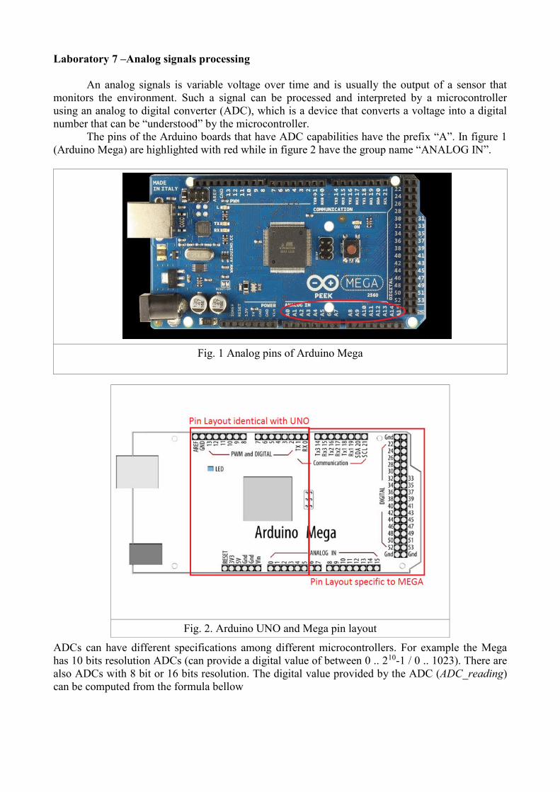
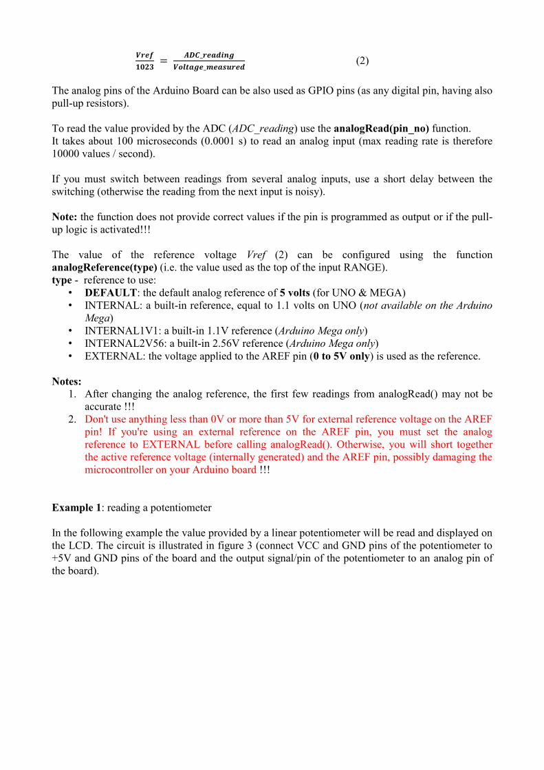
The pins of the Arduino boards that have ADC capabilities have the prefix “A”. In figure 1
(Arduino Mega) are highlighted with red while in figure 2 have the group name “ANALOG IN”.
Fig. 1 Analog pins of Arduino Mega
ADCs can have different specifications among different microcontrollers. For example the Mega
has 10 bits resolution ADCs (can provide a digital value of between 0 .. 210-1 / 0 .. 1023). There are
also ADCs with 8 bit or 16 bits resolution. The digital value provided by the ADC (ADC_reading)
can be computed from the formula bellow
Fig. 2. Arduino UNO and Mega pin layout
𝑽𝒓𝒆𝒇
𝟏𝟎𝟐𝟑 =
𝑨𝑫𝑪_𝒓𝒆𝒂𝒅𝒊𝒏𝒈
𝑽𝒐𝒍𝒕𝒂𝒈𝒆_𝒎𝒆𝒂𝒔𝒖𝒓𝒆𝒅 (2)
The analog pins of the Arduino Board can be also used as GPIO pins (as any digital pin, having also
pull-up resistors).
To read the value provided by the ADC (ADC_reading) use the analogRead(pin_no) function.
It takes about 100 microseconds (0.0001 s) to read an analog input (max reading rate is therefore
10000 values / second).
If you must switch between readings from several analog inputs, use a short delay between the
switching (otherwise the reading from the next input is noisy).
Note: the function does not provide correct values if the pin is programmed as output or if the pull-
up logic is activated!!!
The value of the reference voltage Vref (2) can be configured using the function
analogReference(type) (i.e. the value used as the top of the input RANGE).
type - reference to use:
• DEFAULT: the default analog reference of 5 volts (for UNO & MEGA)
• INTERNAL: a built-in reference, equal to 1.1 volts on UNO (not available on the Arduino
Mega)
• INTERNAL1V1: a built-in 1.1V reference (Arduino Mega only)
• INTERNAL2V56: a built-in 2.56V reference (Arduino Mega only)
• EXTERNAL: the voltage applied to the AREF pin (0 to 5V only) is used as the reference.
Notes:
1. After changing the analog reference, the first few readings from analogRead() may not be
accurate !!!
2. Don't use anything less than 0V or more than 5V for external reference voltage on the AREF
pin! If you're using an external reference on the AREF pin, you must set the analog
reference to EXTERNAL before calling analogRead(). Otherwise, you will short together
the active reference voltage (internally generated) and the AREF pin, possibly damaging the
microcontroller on your Arduino board !!!
Example 1: reading a potentiometer
In the following example the value provided by a linear potentiometer will be read and displayed on
the LCD. The circuit is illustrated in figure 3 (connect VCC and GND pins of the potentiometer to
+5V and GND pins of the board and the output signal/pin of the potentiometer to an analog pin of
the board).
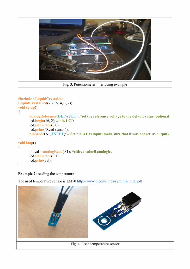
Fig. 3. Potentiometer interfacing example
#include <LiquidCrystal.h>
LiquidCrystal lcd(7, 6, 5, 4, 3, 2);
void setup()
{
analogReference(DEFAULT); //set the reference voltage to the default value (optional)
lcd.begin(16, 2); //init. LCD
lcd.setCursor(0,0);
lcd.print("Read sensor");
pinMode(A1, INPUT); // Set pin A1 as input (make sure that it was not set as output)
}
void loop()
{
int val = analogRead(A1); //citirea valorii analogice
lcd.setCursor(0,1);
lcd.print(val);
}
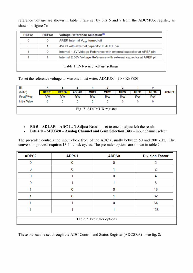
Example 2: reading the temperature
The used temperature sensor is LM50 http://www.ti.com/lit/ds/symlink/lm50.pdf
Fig. 4. Used temperature sensor

Sensor specifications:
• Linear output: +10.0 mV/°C = 0.01V/°C
• Temperature range: −40°C ... +125°C
• +500 mV offset for negative temperatures reading
Fig. 5. Design layout for exemple 2
Example 2 – read temperature, performs an average on 10 consecutive readings, and sends the
result to the PC over the serial connection. Connect the sensor (sensor output connected to A0 pin)
and test the code bellow:
float resolutionADC = .0049 ; // default ADC resolution for the 5V reference = 0.049 [V] / unit
float resolutionSensor = .01 ; // senzsor resolution = 0.01V/°C
void setup() {
Serial.begin(9600);
}
void loop(){
Serial.print("Temp [C]: ");
float temp = readTempInCelsius(10, 0); // read temp. 10 times and returns the average
Serial.println(temp); // display the result
delay(200);

}
float readTempInCelsius(int count, int pin) {
// read temp. count times from the analog pin
float sumTemp = 0;
for (int i =0; i < count; i++) {
int reading = analogRead(pin);
float voltage = reading * resolutionADC;
// subtract the DC offset and converts the value in degrees (C)
float tempCelsius = (voltage - 0.5) / resolutionSensor ;
sumTemp = sumTemp + tempCelsius; // accumulates the readings
}
return sumTemp / (float)count; // return the average value
}
Usage of the ADCs by AVR registers
The ATmega 2560 mC contains a single 10 bit ADC with a maximum sampling freq. of 15kS/s at
the maximum resolution. The sampling method used is the successive approximation.
It offers the possibility to select among 16 input analog pins. A pin is selected through a de-
multiplexing process. Also differential input voltages can be used on 4 independent differential
channels. A simplified schematic of the ADC is shown in figure 6:
Fig. 6. Simplified view of the ADC
The ADC can be used in the following 3 modes:
1. Single conversion: started by writing a logic 1 to the start conversion bit
2. Triggered conversion: the conversion starts on the rising edge of the trigger signal
3. Free running: next conversion starts after the current one is finished
Before using the ADC, the reference voltage and the clock freq. should be set. The options for the
reference voltage are shown in table 1 (are set by bits 6 and 7 from the ADCMUX register, as
shown in figure 7):
Table 1. Reference voltage settings
To set the reference voltage to Vcc one must write: ADMUX = (1<<REFS0)
Fig. 7. ADCMUX register
Bit 5 – ADLAR – ADC Left Adjust Result – set to one to adjust left the result
Bits 4:0 – MUX4:0 – Analog Channel and Gain Selection Bits – input channel select
The prescaler controls the input clock freq. of the ADC (usually between 50 and 200 kHz). The
conversion process requires 13-14 clock cycles. The prescaler options are shown in table 2:
Table 2. Prescaler options
These bits can be set through the ADC Control and Status Register (ADCSRA) – see fig. 8:

Fig. 8. ADCSRA Register
Meaning of the ADCSRA bits:
Bit 7 – ADEN – ADC Enable – Writing this bit to one enables the ADC. By writing it to
zero, the ADC is turned off (pins function become GPIO). Turning the ADC off while a
conversion is in progress, will terminate this conversion
Bit 6 – ADSC – ADC Start Conversion – Write this bit to one starts the first conversion.
The first conversion will take 25 ADC clock cycles instead of the normal 13. This first
conversion performs initialization of the ADC. ADSC will read as one as long as a
conversion is in progress. When the conversion is complete, it returns to zero. Writing zero
to this bit has no effect.
Bit 5 – ADATE – ADC Auto Trigger Enable – When this bit is written to one, Auto
Triggering of the ADC is enabled. The ADC will start a conversion on a positive edge of the
selected trigger signal. The trigger source is selected by setting the ADC Trigger Select bits,
ADTS in ADCSRB.
Bit 4 – ADIF – ADC Interrupt Flag – This bit is set when an ADC conversion completes
and the Data Registers are updated. The ADC Conversion Complete Interrupt is executed if
the ADIE bit and the I-bit in SREG are set. ADIF is cleared by hardware when executing the
corresponding interrupt handling vector. Alternatively, ADIF is cleared by writing a logical
one to the flag.
Bit 3 – ADIE – ADC Interrupt Enable – When this bit is written to one and the I-bit in
SREG is set, the ADC Conversion Complete Interrupt is activated.
Bits 2:0 – ADPS2:0 – ADC Prescaler Select Bits – These bits determine the division factor
between the mC frequency and the input clock to the ADC (Table 2)
ADCL and ADCH – ADC Data Registers
• The conversion result is stored in these registers (fig. 9). If ADLAR is set, the result is left
adjusted. If ADLAR is cleared (default), the result is right adjusted.
• When ADCL is read, the ADC Data Register is not updated until ADCH is read. If the result
is left adjusted and no more than 8-bit precision is required, it is sufficient to read ADCH.
Otherwise, ADCL must be read first, then ADCH.
• The 2 registers combined can be refered by the ADCW name.
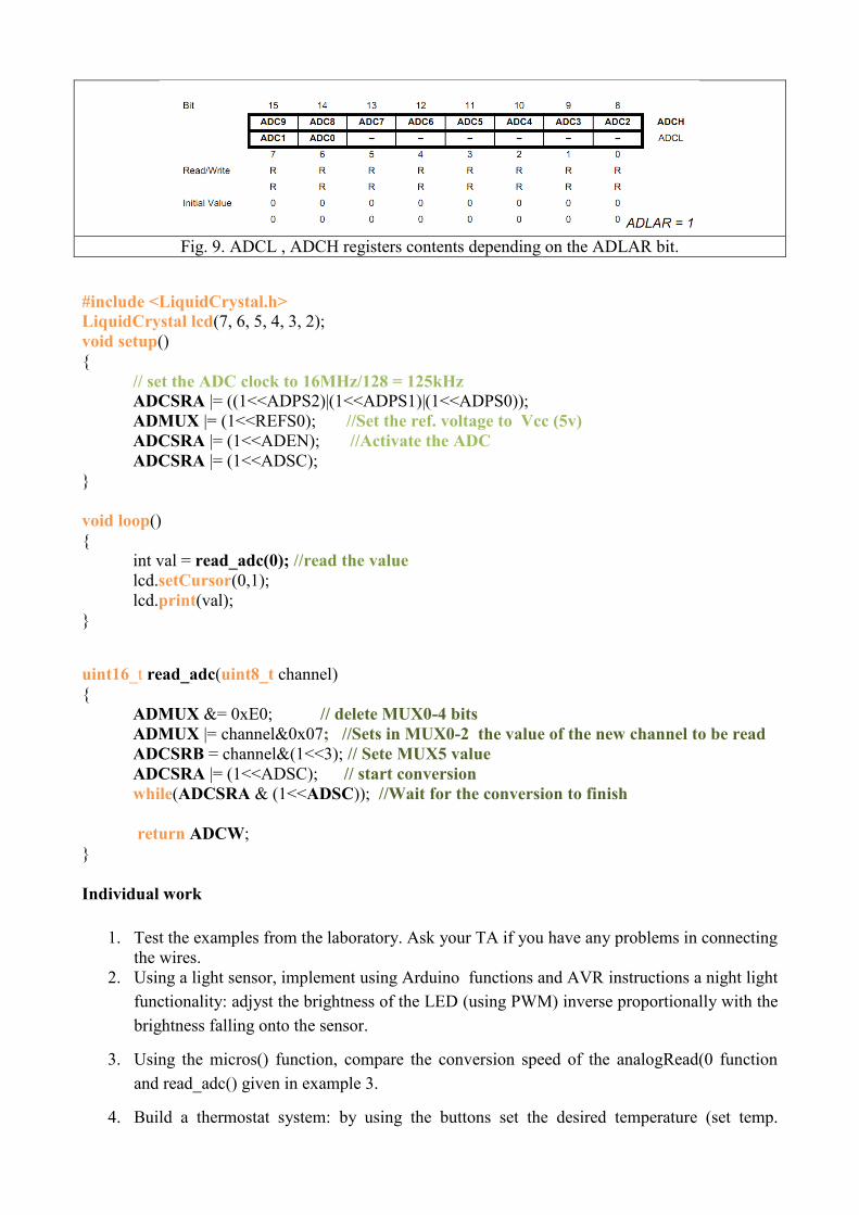
Fig. 9. ADCL , ADCH registers contents depending on the ADLAR bit.
#include <LiquidCrystal.h>
LiquidCrystal lcd(7, 6, 5, 4, 3, 2);
void setup()
{
// set the ADC clock to 16MHz/128 = 125kHz
ADCSRA |= ((1<<ADPS2)|(1<<ADPS1)|(1<<ADPS0));
ADMUX |= (1<<REFS0); //Set the ref. voltage to Vcc (5v)
ADCSRA |= (1<<ADEN); //Activate the ADC
ADCSRA |= (1<<ADSC);
}
void loop()
{
int val = read_adc(0); //read the value
lcd.setCursor(0,1);
lcd.print(val);
}
uint16_t read_adc(uint8_t channel)
{
ADMUX &= 0xE0; // delete MUX0-4 bits
ADMUX |= channel&0x07; //Sets in MUX0-2 the value of the new channel to be read
ADCSRB = channel&(1<<3); // Sete MUX5 value
ADCSRA |= (1<<ADSC); // start conversion
while(ADCSRA & (1<<ADSC)); //Wait for the conversion to finish
return ADCW;
}
Individual work
1. Test the examples from the laboratory. Ask your TA if you have any problems in connecting
the wires.
2. Using a light sensor, implement using Arduino functions and AVR instructions a night light
functionality: adjyst the brightness of the LED (using PWM) inverse proportionally with the
brightness falling onto the sensor.
3. Using the micros() function, compare the conversion speed of the analogRead(0 function
and read_adc() given in example 3.
4. Build a thermostat system: by using the buttons set the desired temperature (set temp.

displayed on the LCD during the setup phase). After the setup phase ends, the LSD will
display the ambient temp. If the ambient temp is smaller then the set one, display on the
LCD “heating”. When the ambient temp. is >= set temp. erase the “heating” message/status
from the display.