lab manual for ece 455 spring, 2011 department of ... · department of electrical and computer...
TRANSCRIPT

Lab Manual for
ECE 455
Spring, 2011
Department of Electrical and Computer
Engineering
University of Waterloo
Written by Bernie Roehl ([email protected])
Version 0
Last updated April 18, 2011
Copyright (c) 2011 by Bernie Roehl.
All rights reserved unless otherwise noted.
NOTE: Students enrolled in ECE courses at the University of Waterloo are authorized to print or duplicate
this lab manual in its entirety for their personal use.
Outline
1) Development Environment Covers how to install the µVision IDE, and how to use it to build and deploy a simple “Hello,
world” example program.
2) Hardware Overview Describes the hardware of the MCB1700 board, focusing on those specific components that you
will be using in your labs.
3) Coding Discusses ways of optimizing your code, and describes the calling conventions used by the C
compiler so you can interface between C and assembly language.
4) Debugging and Simulation Shows how to use the debugging component of the IDE, both with the actual hardware and with
the built-in simulator.
5) Lab Assignment Descriptions Gives a description of each of the labs for your course, including the objectives of each.
Note that this lab manual does not describe the ARM architecture, instruction set, assembly
language syntax, or the C programming language. References for all of those are readily
available online.

Table of Contents
1. Development Environment
Setting Up Your System
A Quick Tour of the IDE
Creating a New Project
Creating Source Files
Building and Running the “Hello world” example
2. Hardware Overview
Major Functional Blocks
Memory
Pin Connect Block
Power Control Block
Vectored Interrupt Controller
General-Purpose I/O
Clocks
Configuration Wizard
ADC
DAC
Timers
MPU
Display
3. Coding
Writing Efficient Code
Calling Conventions
4. Debugging and Simulation
Disassembly and Call Stack Windows
Register Window
Memory and Symbol Table Windows
Watch Window
Peripheral Device Windows
Breakpoints Window
Logic Analyzer
5) Lab Assignment Descriptions
Assignment 1: Hello, World
Assignment 2: Simple Timing
Assignment 3: Polling vs Interrupts
Assignment 4: Reaction Test
Assignment 5: (Yet to come)
6) Closing Comments
Notices Regarding Software, Documents, And Services Available On This Website
Links To Third Party Sites

1. Development Environment
All development for the MCB1700 is done using the Keil µVision IDE. µVision is similar to many
other IDEs you may be familiar with such as Eclipse or Visual Studio. It combines an editor,
compiler, debugger and simulator into a single development environment.
The µVision environment is very generic, and can work with a variety of different processors and
boards. It can also build binaries to run in flash memory, static RAM or a simulator that’s
included with the package.
Depending on your lab, much of the initial development work can be done using the simulator.
You can download the free version of µVision and use it with the simulator on your own
computer, and only use the actual MCB1700 boards for final testing. The only significant
limitation of the free version of the software is that the size of your binary is limited to 32 KB,
which should be adequate for any of our labs.
Setting Up Your System
The µVision software is already installed on the computers in the lab. However, if you are doing
development using your own computer, you will need to install µVision. You can get it from the
following URL:
https://ece.uwaterloo.ca/~ece455/mdk414.exe
When you install µVision, you should ask it to also install the example projects for the “Keil
(NXP) MCB1xxx Boards”. You will also need to let it install the ULINK driver, which
communicates with the Cortex debugger interface on the board using an attached
daughterboard.
The next step is to create a folder for your course, either on your own computer or on your
Nexus P: drive (or your N: drive, if your P: drives is not available for any reason). You can call it
whatever you like, but it should probably be named for the course (e.g. something like
“ece455”). Once you’ve created the folder, download the support files from the following URL:
https://ece.uwaterloo.ca/~ece455/mcb1700_ece.zip
Unzip that file into the folder you created. You are now ready to start creating projects for your
course.
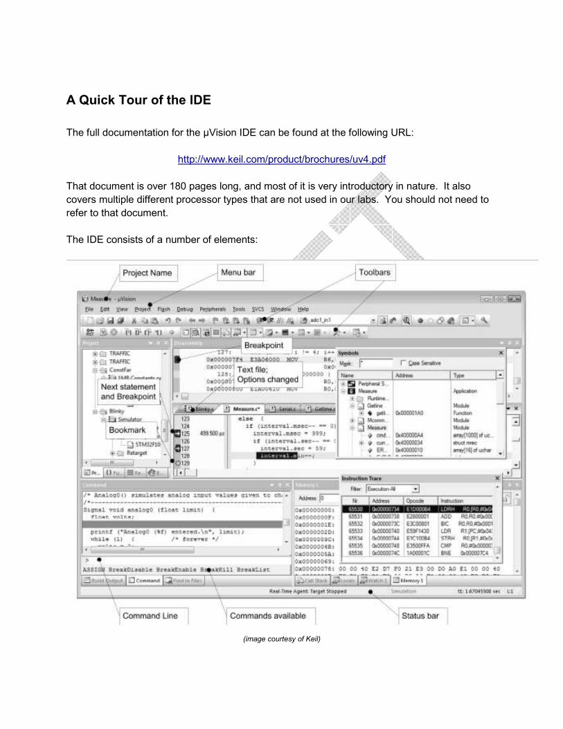
A Quick Tour of the IDE
The full documentation for the µVision IDE can be found at the following URL:
http://www.keil.com/product/brochures/uv4.pdf
That document is over 180 pages long, and most of it is very introductory in nature. It also
covers multiple different processor types that are not used in our labs. You should not need to
refer to that document.
The IDE consists of a number of elements:
(image courtesy of Keil)
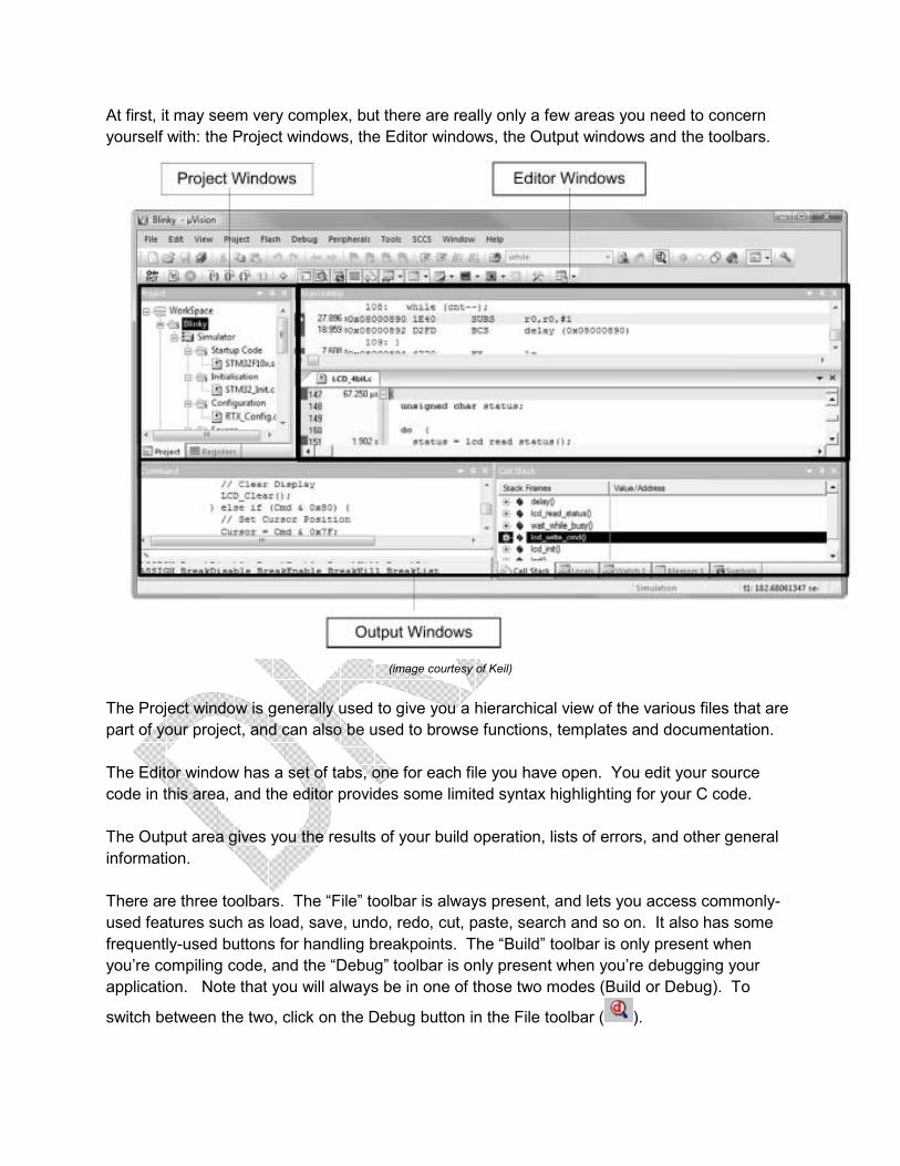
At first, it may seem very complex, but there are really only a few areas you need to concern
yourself with: the Project windows, the Editor windows, the Output windows and the toolbars.
(image courtesy of Keil)
The Project window is generally used to give you a hierarchical view of the various files that are
part of your project, and can also be used to browse functions, templates and documentation.
The Editor window has a set of tabs, one for each file you have open. You edit your source
code in this area, and the editor provides some limited syntax highlighting for your C code.
The Output area gives you the results of your build operation, lists of errors, and other general
information.
There are three toolbars. The “File” toolbar is always present, and lets you access commonly-
used features such as load, save, undo, redo, cut, paste, search and so on. It also has some
frequently-used buttons for handling breakpoints. The “Build” toolbar is only present when
you’re compiling code, and the “Debug” toolbar is only present when you’re debugging your
application. Note that you will always be in one of those two modes (Build or Debug). To
switch between the two, click on the Debug button in the File toolbar ( ).

All the icons in the toolbars have tooltips that appear if you hover over the icon, and the
meaning of each should be clear (e.g. “set breakpoint”).
The individual windows can be dragged around by their title bars, and you can tile the editor
windows to examine multiple source files at the same time. If things get out of hand, you can
use the Window menu item “Reset view to defaults” to get back to a reasonable window layout.
The Debug tools will be discussed later, after we’ve examined the hardware. For now we’ll
focus on the Build process.
Creating a New Project
Launch µVision, and use the menu item Project/New µVision Project to create a new project.
Choose the folder you created for your course, and give your project a name (e.g. “lab1”).
You will then be asked to specify what hardware you’ll be using. Expand the “NXP (founded by
Philips)” tree and select the “LPC 1768” processor. When asked if the startup files should be
copied over and added to your project, choose “yes”.
In the Project window, click on “Target 1” (in the hierarchy tree), then click it again so you can
rename it to something more meaningful such as “LPC1768 Flash”. Expand the target, then
right click on “Source Group 1” and select “Add files to group Source Group 1”. In the resulting
dialog box, under “Files of type:”, choose “All files”. Select "system_LPC17xx" and
"GLCD_SPI_LPC1700" (both are C source files) and “GLCD” (a header file). Click Add, and
then Close.
What you’ve done is create a new project with a new build target (“LPC1768 Flash”), then
added the system startup code, the display routines and the display header file to the project.
At this point, you’re ready to start writing your code.
Creating Source Files
Using the “File/New” menu item, create a new file. It will initially be a “.txt” file, so use “File/Save
as” to save it out with a “.c” extension (e.g. “main.c”). Right click on “Source Group 1” in the
Project window, select “Add files to group Source Group 1”, select your source file, then click
Add and Close. You must do this once for each new source file in your project. Forgetting to do
this is a very common mistake.
Note that you can rename “Source Group 1” to something more meaningful. You can also
rename your target, create additional targets, and so on by right-clicking on the target in the
Project window and selecting “Manage components”.

Building and Running the “Hello world” example
Here is the code for a simple “Hello, world” example:
#include <lpc17xx.h>
#include "glcd.h"
int main(void)
{
SystemInit();
GLCD_Init();
GLCD_DisplayString(0, 0, 1, "Hello, world!");
return 0;
}
The first line brings in the definitions for the various registers that are on the LPC1768 family of
processors. The second line brings in the definitions for the display routines that put text and
graphics on the LCD panel. Obviously the glcd.h file is only needed if you’re using the display.
The very first thing we do in main() is call SystemInit(), which does the initialization for us. If you
open the system_17xx.c file by double-clicking on it in the Project window, then look at the
bottom of the editor window, you should see a “configuration wizard” tab. This wizard allows
you to configure your clock settings as well as the power settings for the on-chip peripherals.
The SystemInit() function is where all that initialization takes place. These settings wil be
discussed in detail in the Hardware section of this manual.
The GLCD_Init() function does the tedious work of initializing the LCD display. The next line
calls the GLCD_DisplayString() function to put a character string on the display at line 0, row 0,
using font 1 (the larger of the two available fonts).
Build your application by hitting F7. If there are no errors, click on the LOAD button( )
to download the code into flash memory on the MCB1700 board. To run it, just hit the button
marked “Reset” on the board.
From within the IDE you can debug your program by single-stepping and setting breakpoints.
You can also simulate the execution of your software without needing to have access to the
board itself. Both of these will be discussed later in this manual, but first we need to become
more familiar with the hardware on the board.

2. Hardware Overview
The board being used in our labs is the Keil MCB1700. It uses the NXP LPC 1768 processor,
consisting of an ARM core (specifically, the Cortex M3), 512 KB of flash memory and 64 KB of
SRAM along with a wide variety of on-chip peripherals.
The board itself is relatively simple, and aside from the LPC 1768 itself there are only a few
support circuits (mostly RS-232 level converters, ethernet transceivers, audio amplifiers and so
on). The board provides a USB port, two serial (COM) ports, two CAN ports, an ethernet
connector, a micro SD card slot, a potentiometer, a speaker and a set of LEDs and buttons. It
also provides a full-colour LCD display.
(image courtesy of Keil)
In our department labs, the board is connected to the host computer using two USB cables.
One simply provides power to the MCB1700, while the other connects to a ULINK-ME
daughterboard that is plugged into the Cortex debugging interface on the MCB1700. It is
through the ULINK-ME that you will be downloading your compiled code and debugging it.
Since all the peripherals are on-chip, your primary reference for the board will be the manual for
the LPC 1768 chip itself. This can be found at the following URL:
http://www.keil.com/dd/docs/datashts/philips/lpc17xx_um.pdf
Note that the document is 840 pages long, and only a small fraction of it is relevant to your labs,
so there is no need to print out the entire document. This lab manual will provide all the
information you need, and will also reference specific sections of the product document which
you can either refer to online or print out if necessary.
Major Functional Blocks
The LPC 1768 is a “system on a chip” that combines flash, SRAM, timers, a DAC, a multi-
channel ADC and numerous communications interfaces onto a single IC.
Note that many of the blocks identified in this next diagram are not used in our labs. In this
manual we will only be discussing those blocks that you will actually be using.
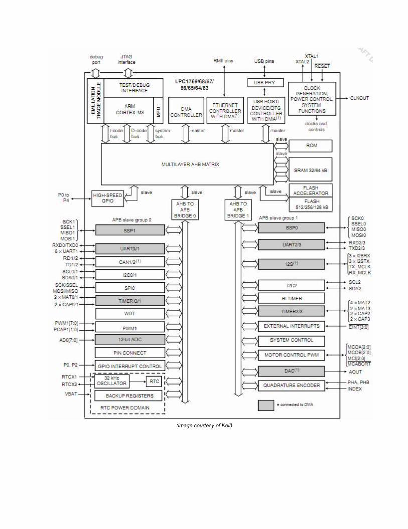
(image courtesy of Keil)
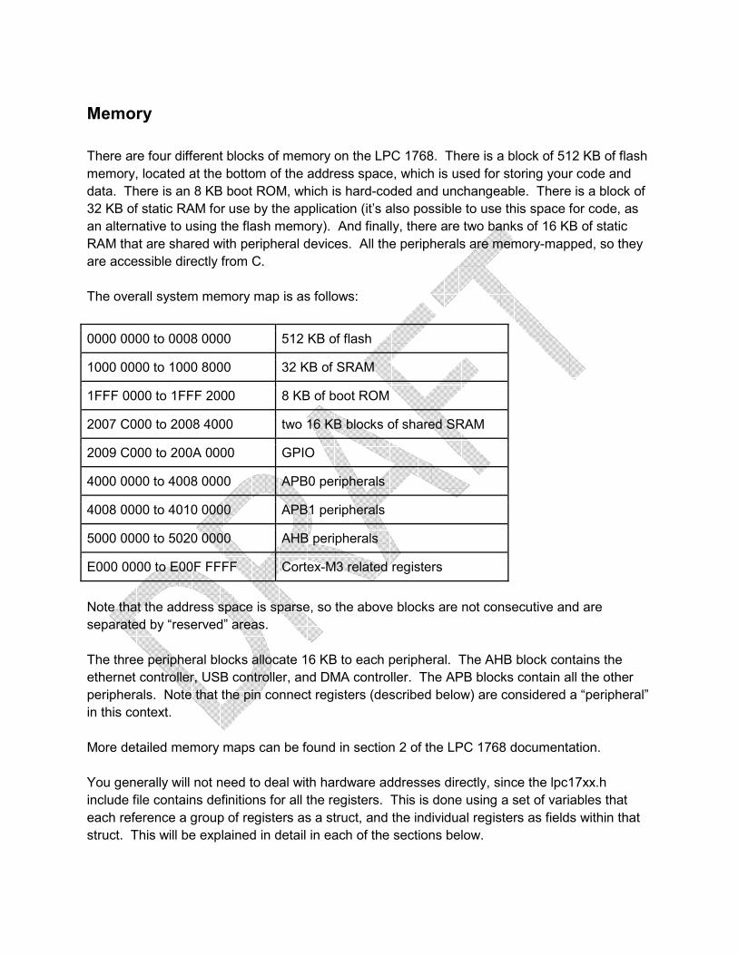
Memory
There are four different blocks of memory on the LPC 1768. There is a block of 512 KB of flash
memory, located at the bottom of the address space, which is used for storing your code and
data. There is an 8 KB boot ROM, which is hard-coded and unchangeable. There is a block of
32 KB of static RAM for use by the application (it’s also possible to use this space for code, as
an alternative to using the flash memory). And finally, there are two banks of 16 KB of static
RAM that are shared with peripheral devices. All the peripherals are memory-mapped, so they
are accessible directly from C.
The overall system memory map is as follows:
0000 0000 to 0008 0000 512 KB of flash
1000 0000 to 1000 8000 32 KB of SRAM
1FFF 0000 to 1FFF 2000 8 KB of boot ROM
2007 C000 to 2008 4000 two 16 KB blocks of shared SRAM
2009 C000 to 200A 0000 GPIO
4000 0000 to 4008 0000 APB0 peripherals
4008 0000 to 4010 0000 APB1 peripherals
5000 0000 to 5020 0000 AHB peripherals
E000 0000 to E00F FFFF Cortex-M3 related registers
Note that the address space is sparse, so the above blocks are not consecutive and are
separated by “reserved” areas.
The three peripheral blocks allocate 16 KB to each peripheral. The AHB block contains the
ethernet controller, USB controller, and DMA controller. The APB blocks contain all the other
peripherals. Note that the pin connect registers (described below) are considered a “peripheral”
in this context.
More detailed memory maps can be found in section 2 of the LPC 1768 documentation.
You generally will not need to deal with hardware addresses directly, since the lpc17xx.h
include file contains definitions for all the registers. This is done using a set of variables that
each reference a group of registers as a struct, and the individual registers as fields within that
struct. This will be explained in detail in each of the sections below.

Pin Connect Block
Because of the large number of internal peripherals, most of the pins on the chip can perform as
many as four different functions. It is therefore necessary for you to specify what function you
want each pin to be used for. This is accomplished by programming a set of registers known as
the Pin Connect Block. For example, pin P0.0 can be used for RD1 (received data on CAN port
1), TXD3 (transmit data on UART 3), SDA1 (part of the I2C interface) or as a general-purpose
input/output pin, depending on the setting of a pin select register. The specifics of selecting
particular pin functions will be discussed as needed in the sections below. You may also need
to set the mode of each pin (internal pull-up resistor, pull-down resistor, or neither).
The pin connect block is referenced from C as a struct called LPC_PINCON, with fields called
PINSEL1, PINSEL2, PINMODE1, PINMODE2, and so on.
Power Control Block
Because the LPC 1768 is designed to be used in mobile devices, power consumption is a key
issue. There is a set of registers that allow an application to enable and disable power to the
main processor as well as each individual on-chip peripheral. By powering down peripherals
that are not used in a particular application, considerable power savings can be achieved.
For our labs, we power the board from the host computer and so power consumption is not an
issue. However, some peripherals default to being “off”, so you will need to use the power
control block to power them up. The specifics of doing this will be addressed in the sections
below.
The 32-bit peripheral power control register is referenced from C as LPC_SC->PCONP.
LPC_SC is a general system-control register block, and PCONP referes to Power CONtrol for
Peripherals.
Note that you can also specify which peripherals should be powered on using the configuration
wizard, described elsewhere in this document.
Vectored Interrupt Controller
All the internal peripherals are capable of generating interrupts. The specific conditions that
produce interrupts can be set individually for each peripheral, and the individual interrupts can
be enabled or disabled using a set of registers.
Writing an interrupt handler in C is very easy -- just create a function with an appropriate name
and it will automatically be used. The name consists of the prefix from the table below, with
“Handler” appended (e.g. TIMER0_IRQHandler).

Int. number Prefix Description
0 WDT_IRQ Watchdog timer (not used by our labs)
1 TIMER0_IRQ Timer 0
2 TIMER1_IRQ Timer 1
3 TIMER2_IRQ Timer 2
4 TIMER3_IRQ Timer 3
5 UART0_IRQ UART 0
6 UART1_IRQ UART 1
7 UART2_IRQ UART 2
8 UART3_IRQ UART 3
9 PWM1_IRQ PWM 1 (unused on MCB1700)
10 I2C0_IRQ I2C 0 (unused on MCB1700)
11 I2C1_IRQ I2C 1 (unused on MCB1700)
12 I2C2_IRQ I2C 2 (unused on MCB1700)
13 SPI_IRQ SPI (used for communicating with LCD display)
14 SSP0_IRQ SSP 0 (unused on MCB1700)
15 SSP1_IRQ SSP 1 (unused on MCB1700)
16 PLL0_IRQ PLL 0 (interrupts not used by our labs)
17 RTC_IRQ Real-time clock
18 EINT0_IRQ External interrupt 0
19 EINT1_IRQ External interrupt 1 (unused on MCB1700)
20 EINT2_IRQ External interrupt 2 (unused on MCB1700)
21 EINT3_IRQ External interrupt 3 (unused on MCB1700) & GPIO interrupt
22 ADC_IRQ ADC end of conversion
23 BOD_IRQ Brown-out detected (not used in our labs)
24 USB_IRQ USB
25 CAN_IRQ CAN
26 DMA_IRQ DMA
27 I2S_IRQ I2S (unused on MCB1700)
28 ENET_IRQ Ethernet
29 RIT_IRQ Repetitive-interrupt timer
30 MCPWM_IRQ Motor control PWM
31 QEI_IRQ Quadrature encoder
32 PLL1_IRQ USB phase-locked loop (interrupt not used in our labs)
33 USBActivity_IRQ USB activity
34 CANActivity_IRQ CAN activity
Note that a particular peripheral can generate its interrupt for a variety of reasons, which are
configured within that peripheral. For example, timers can be configured to generate interrupts
either on match or on capture.
By default, the interrupt vector table is at the very bottom of physical memory (address 0000
0000). However, you can change this location by setting the Vector Table Offset Register
(SCB->VTOR, section 6.4), placing the table anywhere in the lowest 1 GB of address space.
For alignment reasons, it must be located on a 1024 byte boundary. In practice, you will
typically only relocate it to the bottom of SRAM at 1000 0000.
The priorities of the interrupts can be set individually. See sections 6.5.11 to 6.5.19 for details.
A set of functions is available for enabling and disabling specific interrupts, setting their priority,
and controlling their pending status:
void NVIC_EnableIRQ(IRQn_Type IRQn)
void NVIC_DisableIRQ(IRQn_Type IRQn)
void NVIC_SetPriority(IRQn_Type IRQn, int32_t priority)
uint32_t NVIC_GetPriority(IRQn_Type IRQn)
void NVIC_SetPendingIRQ(IRQn_Type IRQn)
void NVIC_ClearPendingIRQ(IRQn_Type IRQn)
IRQn_Type NVIC_GetPendingIRQ(IRQn_Type IRQn)
The IRQn names are just the prefix from the table above with an “n” appended (e.g.
TIME0_IRQn).
You can also trigger any interrupt in software by writing the interrupt number to the NVIC->STIR
register (values up to 111 are permitted).

You must clear interrupt conditions in the interrupt handler. This is done in different ways,
depending on what caused the interrupt. For example, if you have INT0 configured to generate
an interrupt, you would clear it by setting the low-order bit of the LPC_SC->EXTINT register.
Interrupt handling is described in detail in section 6 of the Keil documentation.
General-Purpose I/O
Among the various functions that can be programmed using the pin control block is GPIO, or
general-purpose I/O. GPIO allows individual pins to be used for input or output.
In the case of the MCB1700, the board provides a set of eight LEDs which are connected to
specific pins on the processor. It also provides a “joystick” consisting of four directional buttons
and a center “select” button, as well as a single “INT0” button, all of which are connected to
input pins on the processor.
When the processor powers up or resets, the pins that are connected to the LEDs and buttons
are automatically configured as GPIO (General-Purpose I/O). However, it is good practice to
configure these pins before using them. In any case, it is also necessary to set the data
direction register to indicate which pins are to be used for input (the buttons) and which for
output (the LEDs). The GPIO control registers are accessed using structs called LPC_GPIO1
and LPC_GPIO2.
Configuring the INT0 button for input is done like this:
LPC_PINCON->PINSEL4 &= ~(3<<20); // P2.10 is GPIO LPC_GPIO2-
>FIODIR &= ~(1<<10); // P2.10 is input
The first line above enables the INT0 button to be used for input by setting bits 21 and 20 of the
PINSEL4 register (section 8.5.5) to zero, which corresponds to GPIO. The second line sets bit
10 in the GPIO2 I/O direction register (section 9.5.1) to zero, meaning the pin will be used for
input. In theory you could omit these two lines, since zero is the default value for both of these
registers.
Setting up the “joystick” is done as follows:
LPC_PINCON->PINSEL3 &= ~((3<< 8)|(3<<14)|(3<<16)|(3<<18)|(3<<20));
/* P1.20, P1.23..26 is GPIO (Joystick) */
LPC_GPIO1->FIODIR &= ~((1<<20)|(1<<23)|(1<<24)|(1<<25)|(1<<26));
/* P1.20, P1.23..26 is input */
The first line of code sets five specific bits in the LPC_PCON->PINSEL3 register (section 8.5.4)
to zero, again meaning that they will be used for general purpose I/O. The second line clears

bits in the I/O direction register, indicating that the five buttons of the “joystick” are to be used for
input. Again, these steps could be omitted since zero is the default value.
Configuring the LEDs for output is straightforward:
LPC_GPIO1->FIODIR |= 0xB0000000; // LEDs on PORT1
LPC_GPIO2->FIODIR |= 0x0000007C; // LEDs on PORT2
These two lines simply set the pins corresponding to the LEDs to be output by turning on the
corresponding bits in the I/O direction register (section 9.5.1).
Notice that in this case we didn’t bother explicitly setting the pins to be GPIO. We didn’t need to
do that in the earlier code either, since GPIO is the default setting.
To turn on a particular LED, you would use the following code:
const U8 led_pos[8] = { 28, 29, 31, 2, 3, 4, 5, 6 };
mask = 1 << led_pos[led];
if (led < 3) LPC_GPIO1->FIOSET = mask;
else LPC_GPIO2->FIOSET = mask;
Notice that the LEDs are split over two separate GPIO ports, with the first three on GPIO port 1
and the remaining five on GPIO port 2. See section 9.5.2 for details.
All the joystick buttons are on GPIO port 1 (section 9.5.4), so to read the “joystick” you would
simply do this:
kbd_val = ~(LPC_GPIO1->FIOPIN >> 20) & 0x79;
The INT0 button is on GPIO2, so reading it is just:
int0_val = ~(LPC_GPIO2->FIOPIN >> 10) & 0x01;
You can enable interrupts from any pin on port zero or port 2, triggered on the rising and/or
falling edge. This is enabled using registered in the LPC_GPIOINT block called IO0IntEnf,
IO0IntEnr, IO2IntEnf and IO2IntEnr (the ‘f’ stands for falling edge, and the ‘r’ stands for rising
edge). The GPIO shares the vector for External Interrupt 3, so that’s what you should enable.
For example, the following code enables an interrupt on the falling edge of pin P2.10 (which
happens to be the INT0 button on the board):
LPC_GPIOINT->IO2IntEnF |= 1 << 10; // falling edge of P2.10
NVIC_EnableIRQ(EINT3_IRQn);
In your interrupt handler you should clear the interrupt condition by writing 1 bits to the
appropriate IntClr register. In this particular case you would do the following:
LPC_GPIOINT->IO2IntClr |= 1 << 10; // clear interrupt condition
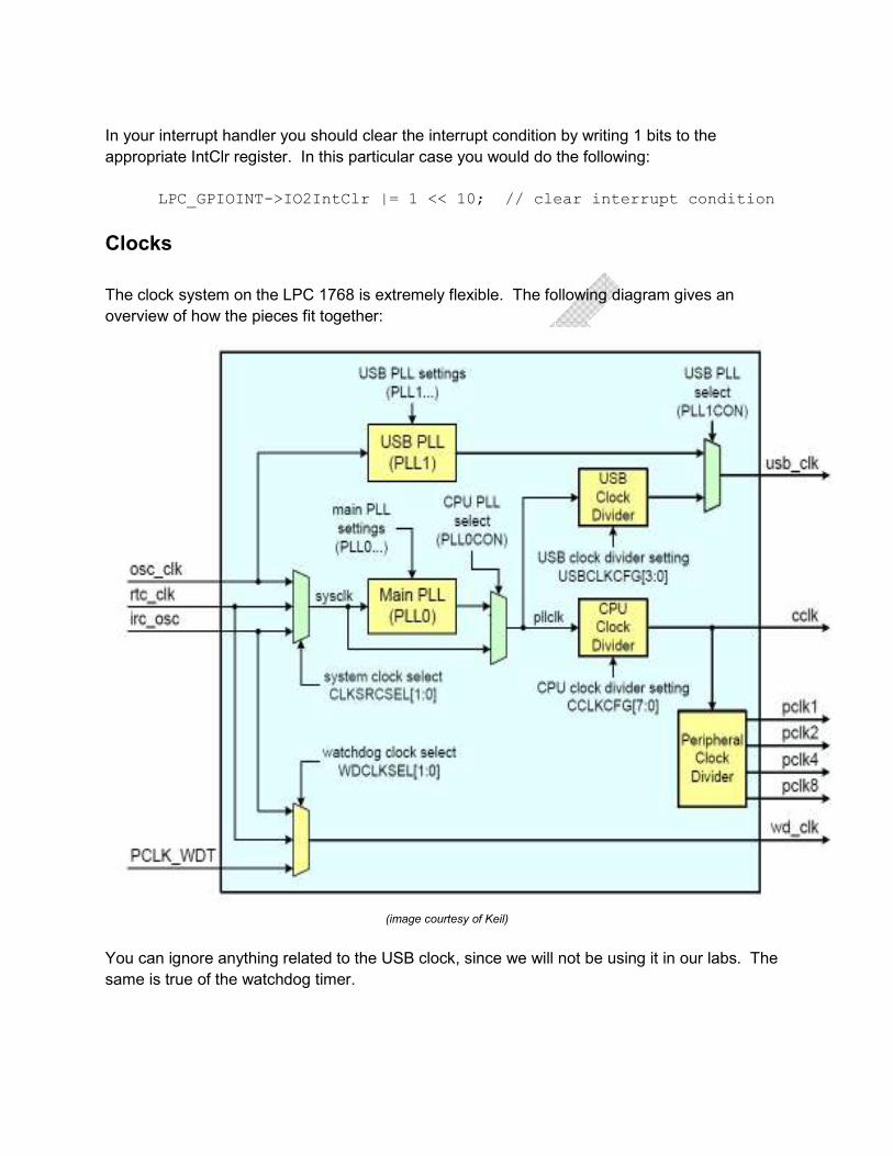
Clocks
The clock system on the LPC 1768 is extremely flexible. The following diagram gives an
overview of how the pieces fit together:
(image courtesy of Keil)
You can ignore anything related to the USB clock, since we will not be using it in our labs. The
same is true of the watchdog timer.

You can select any of three different clock sources by setting the bottom two bits of the
LPC_SC->CLKSRCSEL register (section 4.4.1) as follows:
00 internal 4 MHz RC oscillator (this is the default)
01 12 MHz external oscillator
10 32 KHz realtime clock oscillator
Regardless of which clock source is used, it can either be used directly or as the input to a
phase-locked loop that scales it up to a higher frequency (that still follows the phase of the input
clock) and then divides it down to a lower frequency. There are many configuration options for
the PLL, which are beyond the scope of this lab manual but which are described in section 4.5
of the LPC 1768 documentation.
The input clock (or the output of the PLL, if used) is then put through by a divider whose value is
stored is bits 7:0 of the LPC_SC->CCLKCFG register (see section 4.7.1). If the PLL is used,
the divisor value in CCLKCFG must be at least 2. The output from that divider is the actual
CCLK signal to the processor.
That processor clock signal is further subdivided by 2, 4 and 8 to provide four separate
peripheral clocks (including the original, undivided processor clock signal), and each peripheral
device on the chip can be configured to use any of those four clocks for its operation (see
section 4.7.3 for details on which bits in the LPC_SC->PCLKSEL0 and LPC_SC->PCLKSEL1
registers control the clock selection for each peripheral).
Configuration Wizard
Setting all these values, particularly those of the PLL, is a complex operation that involves
(among other things) waiting for the PLL to lock onto the incoming frequency. Fortunately,
much of this complexity is handled by the startup code that is included with the development kit.
You do not even have to modify that startup code by hand, since the µVision IDE (described
earlier) provides a configuration wizard that handles the updating of the startup code. All you
need to do is choose appropriate settings. Double-click the system_17xx.c file in the Project
window to open it in the editor, then click on the “Configuration Wizard” tab below the file in the
editor window.

Most of the settings are straightforward. Since the MCB1700 is powered from the host
computer, there is no reason not to use the main (external) oscillator. Therefore the oscillator
enable (OSCEN) bit should be set. The OSCRANGE should be set to “1 MHz to 20 MHz” to
match the 12 MHz crystal on the board.
The PLL should be configured to use the oscillator as its input. The main parameters that should
be set for PLL0 are M and N, the multiplier and divisor. The output frequency will be 2*M*F/N,
where F is the input frequency. When using the oscillator, M should not be less than 6 or
greater than 512, and N should always be in the range 1 to 32. In the example shown above, M
is set to 100 and N is set to 6. Therefore, the 12 MHz oscillator will produce an output
frequency from the PLL of 2 * 100 * 12 / 6 = 400 MHz.
Since the CCLKSEL value is 4 (which is set into the bottom 8 bits of the LPC_SC->CCLKCFG
register during system initialization), the CCLK will be 100 MHz (i.e. 400 MHz divided by 4).

The four peripheral clocks would be 100 MHz, 50 MHz, 25 MHz and 12.5 MHz, and you can
configure any peripheral to use any of these four clocks (using the two Peripheral Clock
Selection Registers in the wizard).
Note that these are all good values to use, and you should simply use them unless you have a
specific reason not to.
ADC
The LPC 1768 provides a 12-bit analog to digital converter, with an 8-input analog mux and a
separate capture register for each of those inputs. It is therefore possible to automatically
capture from up to 8 analog sources, each to its own register. On the MCB1700 board, there is
a potentiometer connected to analog input 2, which is most likely the only one you will be using
in your labs.
Since we are just using a single input, you will only need to concern yourself with three
registers:
● the analog/digital control register (LPC_ADC->ADCR, section 29.5.1)
● the analog/digital global data register (LPC_ADC->ADGDR, section 29.5.2)
● the analog/digital interrupt enable register (LPC_ADC->ADINTEN, section 29.5.3)
Initializing the ADC consists of a series of steps:
LPC_PINCON->PINSEL1 &= ~(3<<18);
LPC_PINCON->PINSEL1 |= (1<<18); // P0.25 is AD0.2
LPC_SC->PCONP |= (1<<12); // Enable power to ADC block
LPC_ADC->ADCR = (1<<2) | // select AD0.2 pin
(4<<8) | // ADC clock is 25MHz/5
(1<<21); // enable ADC
Again we see the use of the PINSEL registers. In this case, we clear the bits to zero and then
set the lower bit, so we’re specifying function 0x01 (analog input) for the P0.25 pin. We also
see the first example of using the Power Control registers, since we need to enable power to the
ADC peripheral block before it can be used (see section 4.8.9 for details). Note that this can
also be done using the configuration wizard, described earlier.
We set bits 7:0 of the ADCR register to 00000100, to enable conversion of input 2 to the analog
mux. In hardware-scan mode (which we’re not using, since we only have a single input) you
could set more than one bit to automatically sample more than one channel sequentially.

The ADC uses a successive-approximation approach, and therefore is driven internally by a
clock. We set bits 15:8 of the ADCR register to 4, in order to divide the 25 MHz clock by 5 (the
divisor is the value in the ADCR register plus one, since division by zero is meaningless). Note
that the 25 MHz frequency is provided by choosing the third peripheral clock in the configuration
wizard, which divides the 100 MHz processor clock by 4 as described in the Clocks section
above.
We also turn on the PDN bit (bit 21) of the ADCR register to enable the ADC subsystem itself.
To actually capture data, we would do this:
LPC_ADC->ADCR |= (1<<24);
which starts the A/D conversion (i.e. we write 001 to bits 26:24). We then poll until the
conversion is complete, and retrieve the value:
while (LPC->ADGDR & 0x8000 == 0); // wait for conversion complete
value = (LPC_ADC->ADGDR>>4) & 0xFFF; // read result
There is a data register for each input channel, as well as a global data register that always
stores the most recently converted value regardless of channel. Since we only have the one
analog input, we simply use that global register. The top bit of the register indicates when the
conversion is done, and bits15:4 store the actual 12-bit value.
Alternatively, we can set up the ADC to generate an interrupt whenever a conversion is
complete:
LPC_ADC->ADINTEN = (1<<8); // global enable interrupt
NVIC_EnableIRQ(ADC_IRQn); // enable ADC Interrupt
The ADINTEN register specifies which of the 8 A/D channels should generate interrupts. In this
case we’re setting bit 8, which means that we should generate an interrupt when any of the
channels captures a value.
The NVIC_EnableIRQ() function tells the vectored interrupt controller to recognize interrupts
from the ADC subsystem itself.
We can read the conversion result in the interrupt handler, and possibly start another
conversion going. Alternatively, we could start conversion in a timer interrupt and read the
value in the ADC interrupt handler, thereby ensuring a constant sampling rate. It’s also possible
to have a hardware timer trigger a conversion (see section 29.6.1 for details).
DAC
The LPC 1768 has a 10-bit digital-to-analog converter that uses an internal resistor string,
capable of an update rate of 1 MHz.
In the case of the MCB1700 board, the DAC is connected directly to an amplifier and speaker.
You can produce sound by writing data to the DAC at an suitable rate.
To initialize the DAC, you need to set the appropriate bits in the pin control block, and set the
pin mode to use neither pull-up nor pull-down resistors:
LPC_PINCON->PINSEL1 &= ~(3<<20);
LPC_PINCON->PINSEL1 |= (2<<20);
LPC_PINCON->PINMODE1 &= ~(3<<20);
LPC_PINCON->PINMODE1 |= (2<<20);
To output a value via the DAC, simply write it into bits 15:6 of the LPC_DAC->DACR register
(section 30.4.1). All other bits should be zero.
LPC_DAC->DACR = (value & 0x3FF) << 6;
Note that we mask the value to 10 bits and shift it into the correct position.
Timers
There are four general-purpose 32-bit timer/counters on the LPC 1768. Each of them has a 32-
bit prescaler, a pair of capture registers and four match registers, and can generate interrupts
on various conditions. In our labs, we don’t use the counter, capture or external match
functionality since we don’t typically hook up external signals to the processor pins.
The timers are reference using the LPC_TIMx structs, where x is 0 through 4. Each timer can
be enabled by setting bit 0 in its control register (LPC_TIMx->TCR, section 21.6.2) and reset by
setting and then clearing bit 1. The timer value can be read or written using the timer/counter
register (LPC_TIMx->TC, section 21.6.4), the prescaler divisor can be read and written in the
prescale register (LPC_TIMx->PR, section 21.6.5), and the current prescaler value can be read
and written in the prescale counter register (LPC_TIMx->PC, section 21.6.6). These are all 32-
bit values.
Keep in mind that you can specify which peripheral clock is used to drive each timer (see the
description in the Clocks section, above), and that you would typically set this up using the
configuration wizard.
There are four match registers for each timer (LPC_TIMx->MRy, section 21.6.7). There is also
a match control register (LPC_TIMx->MCR, section 21.6.8) which contains three bits for each of
the four match registers. These bits determine what should happen when the timer register
equals the match register. If the low-order bit is set, an interrupt is generated. If the next higher
bit is set, the timer/counter is reset to zero. If the highest-order bit of the three is set, the
timer/counter stops counting.
To initialize a timer and set it to generate an interrupt on match, you would do the following:
LPC_TIM0->TCR = 0x02; // reset timer
LPC_TIM0->TCR = 0x01; // enable timer
LPC_TIM0->MR0 = 2048; // match value (can be anything)
LPC_TIM0->MCR |= 0x03; // on match, generate interrupt and reset
NVIC_EnableIRQ(TIMER0_IRQn); // allow interrupts from the timer
The interrupt handler must clear the interrupt condition. To do this, set one of the bottom four
bits of the LPC_TIMx->IR register to clear the corresponding match interrupt condition:
LPC_TIM0->IR |= 0x01;
In addition to these four timers, there is a system tick timer (part of the Cortex-M3 core) that is
typically used to provide an interrupt every 10 milliseconds, based on a 100 MHz processor
clock. You enable this by setting the bottom two bits of the system tick control register
(STCTRL, section 23.5.1), with bit 0 enabling the timer and bit 1 enabling the interrupt.
Alternatively, you can initialize it using the SysTick_Config() function which takes the number of
ticks per second as a parameter. One way to set this value is as a fraction of the global
SystemFrequency variable, like this:
SysTick_Config(SystemFrequency/10000);
The SysTick_Handler() routine gets called on system tick interrupts.
And finally, there’s a repetitive interrupt timer. You simply set the RI compare register
(LPC_RIT->RICOMPVAL, section 22.3.1), and an interrupt will be generated whenever the RI
counter LPC_RIT->RICOUNTER reaches that value. You can also write a mask register
(LPC_RIT->RIMASK, section 22.3.2) that causes the compare to always match on the
corresponding bits.
MPU
The LPC 1768, like all Cortex M3 based processors, has a built-in Memory Protection Unit. This
unit is used to restrict access to up to 8 different (and possibly overlapping) blocks of the
address space, by generating a fault when those blocks are accessed inappropriately.

By default, the MPU is disabled. To enable it, you set the bottom bit of MPU->CTRL (section
34.4.5.2). Note that you should first define a number of memory regions, otherwise all memory
access will generate a fault. Alternatively, you can set bit 2 of the MPU->CTRL register to allow
privileged software to continue operating, using the default memory map. You can then define
regions that override that default map.
MPU->CTRL |= 0x05; // enable MPU and allow use of default map
To define a region, you first select it by writing the region number (0 through 7) into the MPU
Region Number Register (MPU->RNR, section 34.4.5.3). You then write values to the MPU
Region Base Address Register (MPU->RBAR, section 34.4.5.4) and the MPU Region Attribute
and Size Register (MPU->RASR, section 34.4.5.5).
Bit 0 of the RASR is used to enable the memory region (or disable it, if the bit is cleared). You
can define regions of various sizes, but they must all be a power of two (anything from 32 bytes
to 4 gigabytes). The size of the region is stored in bits 5:1 of the RASR register, expressed as
the log2 of the size, minus 1. For example, the size of a 1024 byte region would be stored as 9
(log2 of 1024 is 10, minus 1 gives 9).
The base address of the region is stored in the RBAR register, in the top N bits (where N is log2
of the region size). In the example above, the top 10 bits of the RBAR register would be used to
store the region size.
Here’s what all this looks like in code:
region_base_address = 0x10000000; // start of RAM
region_size = 10; // 1024 byte region
MPU->RNR = 1; // select region 1
MPU->RBAR = region_base_address << (32-region_size);
MPU->RASR = ((region_size-1_<<1)|0x01; // store size, enable
By default, any access to a protected region will generate a fault. If you need more precise
control, you can set additional access control bits in the RASR. This is described in section
34.4.5.5 of the LPC 1768 documentation.
Note that if regions overlap, the higher region numbers (up to region 7) take precedence over
the lower region numbers.
You can also disable certain subregions within a region. If you need this capability, refer to
section 34.4.5.8.3 of the documentation.
Display
The MCB1700 board comes with a 320 by 240 TFT LCD display with 16 bits per pixel. The
LPC 1768 communicates with the display over the SPI (Serial Peripheral Interconnect) bus.
This is one of several interconnection buses that the LPC 1768 provides, and it’s the only one
that will be used in our labs. The details of interfacing to the display are fairly involved, but
fortunately you do not need to concern yourself with them. A set of routines is available to
perform the following functions:
void GLCD_Init(void);
void GLCD_SetTextColor(unsigned short color);
void GLCD_SetBackColor(unsigned short color);
void GLCD_DisplayChar(unsigned int row, unsigned int column,
unsigned char font, unsigned char c);
void GLCD_DisplayString(unsigned int row, unsigned int column,
unsigned char font, unsigned char *s);
void GLCD_Clear(unsigned short color);
void GLCD_ClearLn(unsigned int row, unsigned char font);
void GLCD_PutPixel(x, y); // uses current foreground (text) colour
void GLCD_Bitmap(unsigned int x, unsigned int y,
unsigned int w, unsigned int h, unsigned char *bitmap);
void GLCD_ScrollVertical(unsigned int delta_y);
The “font” is either 0 or 1 to select differently-sized characters. The colors can be the
predefined constants Black, Navy, DarkGreen, DarkCyan, Maroon, Purple, Olive, LightGrey,
DarkGrey, Blue, Green, Cyan, Red, Magenta, Yellow and White, or any RGB value packed into
16 bits in 5:6:5 format (i.e. red in bits 15:11, green in bits 10:5 and blue in bits 4:0).
3. Coding
In this section, we’ll be providing hints and suggestions to help you write better code and access
some of the more advanced features of the Cortex-M3 core that is inside the LPC 1768. A
complete description of the ARM C compiler can be found here:
http://infocenter.arm.com/help/index.jsp?topic=/com.arm.doc.kui0097a/armcc_babdidhg.htm
In this manual, we will cover only a few of the more important aspects. You are encouraged to
refer to the above document for more details.
Writing Efficient Code
Even though the compiler does an excellent job of optimizing your code as it compiles it, there
are things you can do to help.
Interrupt handlers should be kept short. Do not do any lengthy calculations in a handler, just
collect data or update values as needed. For maximum speed, put the interrupt handlers in
SRAM rather than flash. You can do this by right-clicking on the source file in the Project
window, selecting “Options for file” and then specifying the memory assignment.
Any variables that are changed in an interrupt handler or are updated by hardware should be
declared volatile to prevent the compiler from performing inappropriate optimizations.
Local variables will typically be assigned to registers, but you can hint this to the compiler by
declaring the variables to be automatic. Both automatic variables and function parameters are
kept in 32-bit registers, so it’s most efficient to make those variables and parameters 32-bit
types as well.
In a struct, it’s most efficient to put the scalars (ints, floats, etc) near the start of the struct so that
shorter address offsets may be used. These can be followed by arrays and other complex data
types.
Try to write your loops in count-down-to-zero form and use simple termination conditions. Try to
use counters of type unsigned int, and test for not equal to zero.
You can use #pragma Ospace to optimize the subsequent function for space, or #pragma Otime
to optimize for speed. You can use #pragma unroll_completely to force loop unrolling.
Depending on the size of your data, you may need to optimize your code for size in order to fit
within the 32 KB limit of the free version of the µVision IDE.

Calling Conventions
The calling conventions follow the ARM ABI (Application Binary Interface). The full description
of the ABI is lengthy and complex, and can be found at:
http://infocenter.arm.com/help/topic/com.arm.doc.ihi0042d/IHI0042D_aapcs.pdf
However, the basics are quite simple:
Registers R0 through R3 are used to pass parameters to the function. Within a function, those
registers can be used for any purpose and do not need to be preserved.
Registers R4 through R11 must be preserved by the called function. If you use them, you
should push the values on the stack at the start of your function and pop them at the end.
Registers R12 through R15 have special purposes. R13 is the Stack Pointer (SP), R14 is the
link register (LR) and R15 is the Program Counter. You must preserve the link register if you
plan to call any functions, since it is used for storing your own function’s return address.
The function value is returned in register R0.
For example, the following line:
GLCD_DisplayString(0, 0, 1, "Hello, world!");
generates the following code:
ADR r3,{pc}+2
MOVS r2,#0x01
MOVS r1,#0x00
MOV r0,r1
BL.W GLCD_DisplayString
The BL instruction (Branch and Link) stores the return address in the link register (LR). This
minimizes use of the stack and makes function calls less expensive.
The GLCD_DisplayString() function starts off like this:
PUSH {r4-r8,lr}
and ends like this:
POP {r4-r8,pc}

In other words, on function entry, registers R4 through R8 are stored on the stack along with the
return address in register LR. On function exit, the R4 through R8 registers are restored from
the stack, and the return address is popped into the program counter (causing a return from the
function).
You can embed assembly language functions in your C source code by using the __asm
keyword, as follows:
__asm void my_add(int alpha, int beta)
{
add r0,r1
bx lr
}
Note that inline assembly is not supported, only embedded assembly as shown above.
4. Debugging and Simulation
The µVision IDE includes an integrated debugger which communicates with the MCB1700 using
a Cortex Debug interface. The debugger can also be configured to use a built-in simulator, to
allow you to develop and test your software even if you don’t have physical access to the
MCB1700 board.
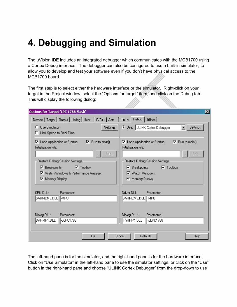
The first step is to select either the hardware interface or the simulator. Right-click on your
target in the Project window, select the “Options for target” item, and click on the Debug tab.
This will display the following dialog:
The left-hand pane is for the simulator, and the right-hand pane is for the hardware interface.
Click on “Use Simulator” in the left-hand pane to use the simulator settings, or click on the “Use”
button in the right-hand pane and choose “ULINK Cortex Debugger” from the drop-down to use
the hardware interface. You should probably choose “Run to main()”, so you can skip stepping
through the initialization sequence.
Most of the settings can be left unchanged, though you may want to check to make sure they’re
similar to the ones in the figure above. Click OK to close the dialog.
Assuming you’ve already built your program (and loaded it into flash, if you’re running on the
hardware instead of the simulator), you can begin your debugging session by clicking on the
Debug button ( ).
At this point your windows will be reconfigured into debug mode. To return to build mode, just
click the Debug button again.
Note that when you view your source code while in debug mode, the current location of the
program counter is indicated with a yellow arrow. You can set or clear breakpoints in your code
by clicking on them in the left-hand margins (in either your original C source code, or in the
disassembly window). A red highlight in the margin indicates the breakpoint.
Take a moment to go through the icons in the Debug toolbar. Hover over each one to get a
tooltip that describes what the button does as well as any keyboard shortcut it may have.
The buttons toward the left of the toolbar are used to reset the processor, run the application
from the current location, stop the application, single-step the next instruction, single step but
skip over subroutine calls, run until a return to the caller is executed, or run until the current line.
The remaining buttons are used to toggle the visibility of various debugging windows that let you
examine and change registers, view and modify memory, watch particular variables, see the
data sent to the serial ports, examine the symbol table, and perform many other functions.
A complete discussion of all the different windows is beyond the scope of this lab manual.
However, there are a few that are particularly useful.
Disassembly and Call Stack Windows
This window shows you the actual assembly language produced for each line in your original C
source code. As with the editor window, a yellow arrow indicates the current instruction and red
highlights in the margin indicate breakpoints
The call stack window shows you a hierarchical tree of functions calls from the main() routine all
the way down to whatever routine you’re executing at the moment. You can click on any
element in the call stack tree to see the values of each parameter that was passed to it.

Register Window
The register window not only displays the contents of all the ARM processor registers, it also
allows you to modify their values. This can be very handy for debugging. Recall from the
Coding section of this manual that parameters are passed to functions in the R0 through R3
registers, and the return address is in the Link Register (R14). The stack pointer is in R13 and
the program counter is in R15.
You can also expand the PSR (Program Status Register) in order to examine and modify the
individual bits.
Memory and Symbol Table Windows
The memory window lets you view any block of memory you like, and directly modify individual
values. Right-clicking will bring up a context menu that will let you select what format to view
the memory in (ASCII, float, double, signed and unsigned char, int, short or long in either hex or
decimal). This window is most useful in conjunction with the symbol table window.
The symbol table window shows you the names of all your global symbols, including variables
and functions, as well as the actual memory address of each. You can put in expressions to
filter the list ($ matches any character, # matches any digit, * matches zero or more characters).
You can drag symbols into other windows (such as the memory window) to view them there.
Note that the memory window is not normally updated in realtime. You can enable periodic
updating using the View/Periodic Window Update menu item.
Watch Window
The watch window lets you essentially set a breakpoint that gets triggered whenever a particular
variable is modified. This is useful if you find a variable contains an unexpected value, and you
want to know where that value came from.
Peripheral Device Windows
There are also windows for many of the peripheral devices. These do not have dedicated
toolbar buttons, but are found in the menu bar under Peripherals. Among other things, you can
examine the pin connect block, the nested vectored interrupt controller, the GPIO registers,
timers, clocks, ADC and DAC converters and all the other capabiltiies of the LPC 1768
processor.
Note that the LCD display is not supported in the simulator.
Breakpoints Window
You can view all your breakpoints and modify their parameters by using ctrl-B or the
Debug/Breakpoints menu item. This is a very powerful feature, which allows you to create a
variety of conditional expressions for triggering a breakpoint. Most of these features are beyond
the scope of this lab manual, but the breakpoints window itself has built-in help to explain its
capabilities and how to use them.
Logic Analyzer
The debugger includes a logic analyzer that will allow you to study the relative timing of various
signals and variable changes. It’s activated using the button in the debugger.
The logic analyzer is mostly self-explanatory. Use the Setup button to add channels. You can
use symbolic names such as FIO1PIN to determine what registers or variables to watch, and
you can specify a mask value (which is ANDed with the contents of the register or variable) and
a right shift value (which is applied after the AND operation). You can view the result as a
numeric value (“analog”) or as a bit value. At any point you can stop the updating of the screen
(and/or stop the simulation itself), and change the resolution to zoom in or out. You can also
scroll forward and backward in time using the scrollbar below the logic analyzer window. There
are also “prev” and “next” buttons to move quickly from one transition to another.
There are currently some issues with saving and loading the channel configurations, but
channels can be set up very quickly and you typically won’t need to watch more than two or
possibly three at once.
5) Lab Assignment Descriptions
ECE 455 consists of five lab assignments and an open project. Here are the descriptions of the
labs.
Assignment 1: Hello, World
Objective: At the end of this lab, you should be familiar with the development environment and
know how to build, download and run a simple “Hello, World” example.
Tasks: Refer to the first section of this lab manual for details. To successfully complete this lab,
you must display the words “Hello, world” on the LCD display of the MCB1700 board.
Assignment 2: Simple Timing
Objective: At the end of this lab, you will be familiar with two different approaches to measuring
the passage of time. You will also have discovered the difficulties involved in getting precise
timing without using hardware support.
Tasks:
1. Implement a function that delays for a given number of milliseconds, using a pair of
nested for() loops. Note that there are several ways of calibrating this loop. Also note
that you should disable interrupts at the start of the loop, and re-enable them at the end,
in order to get more accurate timing.
2. Implement a clock that shows minutes and seconds on the screen, using your delay
function. Let it run for 10 minutes, comparing the value to a stopwatch or wall clock and
noting any discrepencies. In your report, comment on sources of inaccuracy.
3. Implement the clock again, this time using a hardware timer instead of your delay
function. Let it run for 10 minutes, and compare its accuracy to that of the version using
the delay function. Note that there are several ways to implement this, some much more
accurate than others.
Assignment 3: Polling vs Interrupts
Objective: At the end of this lab, you will have compared two different methods of handling user
input and measured the responsiveness of each.

Tasks: This lab requires you to use the software simulator and the built-in logic analyzer.
1. Create a small application which turns out one of the LEDs, polls the INT0 button to
determine when the user has pressed it, and then turns the light on.
2. Create a second small application which does the same thing, but uses interrupts
instead of polling.
Use the logic analyzer to determine the delay in nanoseconds between the user pressing the
button and the light coming on in each version of the application.
In your report, explain what causes the delay in each case. Be sure to include screen captures
of the logic analyzer in each case.
Hints:
● Use the Logic Analyzer to look at the appropriate FIOPIN peripheral registers.
● Use the Peripherals/GPIO Interrupts menu item to get a dialog box that allows you to
trigger the appropriate interrupt in the simulator.
Assignment 4: Reaction Test
Objective: By the end of this lab, you will have successfully implemented a basic reaction timer
using the knowledge gained in the preceeding labs.
Tasks: Implement a reaction test that works as follows:
1. The board is reset
2. The user is prompted to press a key to start
3. After a random delay of 1 to 10 seconds, an LED is lit
4. The user presses a button
5. The application measures the amount of time from the LED being lit to the user pressing
the button
6. The time in milliseconds is displayed on the LCD display, along with the best (fastest)
time so far
7. The user is prompted again (i.e. resume from step 2).
Reactions times of up to 5 minutes should be measurable, to account for users who are easily
distracted. You should try to achieve the most precise timing possible. Document your
maximum measurable reaction time and your resolution, as well as the trade-offs between the
two.
Compute the worse-case execution time, and show timing diagrams.

Assignment 5: (Yet to come)
Work in progress...

6) Closing Comments
This lab manual is a “living document”. If you have any comments, particularly if you find there
is information needed for your labs that is not covered here, please contact the author (Bernie
Roehl, [email protected]).
The online version of this manual will be continually updated, and may change during the
course of a term. You should check back occasionally in case there have been changes. The
“last updated” date on the title page generally indicate when the most recent change was made.

Some of the illustrations and images used in this lab manual are provided by Keil. As required,
here is their copyright notice:
KEIL, ARM, AND/OR THEIR RESPECTIVE SUPPLIERS MAKE NO REPRESENTATIONS ABOUT
THE SUITABILITY OF THE INFORMATION CONTAINED IN THE DOCUMENTS AND RELATED
GRAPHICS PUBLISHED ON THIS SERVER FOR ANY PURPOSE. ALL SUCH DOCUMENTS AND
RELATED GRAPHICS ARE PROVIDED "AS IS" WITHOUT WARRANTY OF ANY KIND. KEIL,
ARM, AND/OR THEIR RESPECTIVE SUPPLIERS HEREBY DISCLAIM ALL WARRANTIES AND
CONDITIONS WITH REGARD TO THIS INFORMATION, INCLUDING ALL IMPLIED
WARRANTIES AND CONDITIONS OF MERCHANTABILITY, FITNESS FOR A PARTICULAR
PURPOSE, TITLE AND NON-INFRINGEMENT. IN NO EVENT SHALL KEIL, ARM, AND/OR THEIR
RESPECTIVE SUPPLIERS BE LIABLE FOR ANY SPECIAL, INDIRECT OR CONSEQUENTIAL
DAMAGES OR ANY DAMAGES WHATSOEVER RESULTING FROM LOSS OF USE, DATA OR
PROFITS, WHETHER IN AN ACTION OF CONTRACT, NEGLIGENCE OR OTHER TORTUOUS
ACTION, ARISING OUT OF OR IN CONNECTION WITH THE USE OR PERFORMANCE OF
INFORMATION AVAILABLE FROM THIS SERVER.
THE DOCUMENTS AND RELATED GRAPHICS PUBLISHED ON THIS SERVER COULD INCLUDE
TECHNICAL INACCURACIES OR TYPOGRAPHICAL ERRORS. CHANGES ARE PERIODICALLY
ADDED TO THE INFORMATION HEREIN. KEIL, ARM, AND/OR THEIR RESPECTIVE SUPPLIERS
MAY MAKE IMPROVEMENTS AND/OR CHANGES IN THE PRODUCT(S) AND/OR THE
PROGRAM(S) DESCRIBED HEREIN AT ANY TIME.
Notices Regarding Software, Documents, And Services
Available On This Website
IN NO EVENT SHALL KEIL, ARM, AND/OR THEIR RESPECTIVE SUPPLIERS BE LIABLE FOR
ANY SPECIAL, INDIRECT OR CONSEQUENTIAL DAMAGES OR ANY DAMAGES WHATSOEVER
RESULTING FROM LOSS OF USE, DATA OR PROFITS, WHETHER IN AN ACTION OF
CONTRACT, NEGLIGENCE OR OTHER TORTUOUS ACTION, ARISING OUT OF OR IN
CONNECTION WITH THE USE OR PERFORMANCE OF SOFTWARE, DOCUMENTS, PROVISION
OF OR FAILURE TO PROVIDE SERVICES, OR INFORMATION AVAILABLE FROM THIS SERVER.
Links To Third Party Sites
THE LINKS IN THIS AREA WILL LET YOU LEAVE THE KEIL WEB SITE. LINKED SITES ARE
NOT UNDER THE CONTROL OF KEIL AND/OR ARM AND KEIL AND/OR ARM ARE NOT
RESPONSIBLE FOR THE CONTENTS OF ANY LINKED SITE OR ANY LINK CONTAINED IN A
LINKED SITE. THESE LINKS ARE PROVIDED TO YOU ONLY AS A CONVENIENCE, AND THE
INCLUSION OF ANY LINK DOES NOT IMPLY ENDORSEMENT BY KEIL OR ARM.
COPYRIGHT NOTICE. Copyright © 2011 Keil - An ARM Company or its suppliers, 4965
Preston Park Road, Suite 650, Plano, Texas, 75093 U.S.A. All rights reserved.
TRADEMARKS. Keil products referenced herein are either trademarks or registered
trademarks of Keil - An ARM Company. Other product and company names mentioned
herein may be the trademarks of their respective owners.

The names of companies, products, people, characters and/or data mentioned herein are
fictitious and are in no way intended to represent any real individual, company, product or
event, unless otherwise noted.
Any rights not expressly granted herein are reserved.
Contact Keil with questions or problems with this service.