lab-in-a-smartphone: image sensor- based …
TRANSCRIPT

LAB-IN-A-SMARTPHONE: IMAGE SENSOR-BASED SPECTROSCOPIC ANALYSIS
By
Saoud Almulla
Senior Thesis in Electrical Engineering
University of Illinois at Urbana-Champaign
Advisor: John Dallesasse
May 2015

ii
Abstract
With their high-resolution cameras and potential for application development, smartphones are proving
to be viable vehicles for low-cost detection tools. As handheld alternatives to traditional measurement
devices, they can be used in settings where laboratories are unavailable. This projects aims to take
advantage of these qualities by developing an inexpensive manufacturable approach to mobile lab
analysis. The proposed device consists of a CMOS image sensor covered by different ranged linear variable
filters (LVFs) and packaged with four light sources. Before designing the final CMOS sensor package, initial
tests had to be made to prove that an LVF-covered CMOS can be used as a viable measurement tool. This
paper discusses the experiments conducted and the results obtained. Two measurement techniques are
considered: Raman and fluorescence spectroscopy. In the experimental setup, spectral data is obtained
by shining a 785 nm laser onto a cuvette filled with an excitable sample of either Rhodamine 6G (Raman)
or near-IR dye (fluorescence). The scattered light is then gathered onto the CMOS sensor and images are
captured. The LVF’s presence on the sensor produces images displaying discrete bands of light on a dark
background. These are processed into the desired spectral graphs and analyzed. Ultimately, the proposed
device will also be designed to perform other tests such as label-free biosensor measurements, and the
excitation of quantum dots.
Subject Keywords: biosensor; spectroscopy; Raman; fluorescence; linear variable filter

iii
Acknowledgments
This research was supported by both the National Science Foundation and the Center for Innovative
Instrumentation Technology.
I would like to thank my advisor Professor John Dallesasse for his guidance throughout the research and
writing processes. Additional thanks go to the members of both Professor Dallesasse and Professor
Cunningham’s groups.
Finally, I would like express my gratitude to my father Abdulaziz Almulla for his unwavering support from
across the Atlantic.

iv
Contents
1. Introduction ............................................................................................................................................ 1
1.1 Motivation ........................................................................................................................................ 1
1.2 Overview ........................................................................................................................................... 2
2. Literature Review .................................................................................................................................... 3
3. Background ............................................................................................................................................. 4
3.1 Linear Variable Filters ....................................................................................................................... 4
3.2 Raman Spectroscopy ......................................................................................................................... 5
3.3 Fluorescence Spectroscopy ............................................................................................................... 6
4. Experiments and Results ......................................................................................................................... 7
4.1. LVF Calibration ................................................................................................................................. 7
4.1.1. Setup ......................................................................................................................................... 7
4.1.2. Results ....................................................................................................................................... 8
4.2 Raman Excitation ............................................................................................................................ 11
4.2.1. Setup ....................................................................................................................................... 11
4.2.2. Results ..................................................................................................................................... 12
4.3 Fluorescence ................................................................................................................................... 13
4.3.1. Setup ....................................................................................................................................... 13
4.3.2. Results ..................................................................................................................................... 13
5. Conclusion............................................................................................................................................. 14
References ................................................................................................................................................ 15

1
1. Introduction
1.1 Motivation More than one-quarter of the global population currently use smartphones. This metric is set to jump to
one third of the total population by 2018 [1]. These devices have become increasingly sophisticated with
every passing generation, currently boasting high-resolution cameras, internet connectivity, and powerful
CPUs among a slew of other features. These are joined by a host of applications that take advantage of
the hardware capabilities of the devices, giving them nearly unlimited potential. In parallel to the constant
growth of the smartphone market, personal healthcare has seen a resurgence with portable devices
starting to become viable alternatives to laboratories and hospitals. Wearables such as the Nike FuelBand
or the Fitbit that interface with smartphones have given the user unprecedented access to medical
information usually only available at yearly checkups. Smartphones have also been used as biochemical
portable diagnostics tools. Research groups have taken advantage of the smartphone’s CMOS sensor in
conjunction with external cradles and optics to perform accurate biological and chemical tests such as the
detection of biomarkers [2], lens-free microscopy [3], and label-free biodetection [4]. Manufacturers are
constantly looking for ways to build on their devices, adding new features alongside hardware
improvements. Incorporating diagnostic testing directly into a new generation of smartphones is a natural
response to the call for freedom in personal healthcare. Such a device could be used for monitoring
personal health, food and drug detection, medical diagnostics in parts of the world lacking quality medical
facilities, and many other applications.
This project looks to take the portable diagnostic tool
one step further by integrating it directly with the
smartphone in the form of a second rear-facing special
purpose CMOS imaging sensor as shown in Figure 1.
The user would simply have to place the device against
a sample and perform the desired tests through a
software interface. In the first phase of the project, the
goal is to demonstrate an inexpensively manufacturable approach to mobile lab analysis by developing a
low-cost CMOS image sensor that can be integrated to smartphones turning them into portable diagnostic
tools.
Figure 1. Concept of Lab-in-a-Smartphone capability incorporated into a mobile device.

2
1.2 Overview The CMOS image sensor is a two-dimensional array of pixels that is covered with three Linear Variable
Filters (LVF). The LVFs are designed to cover separate wavelength bands. This allows the chip to operate
as a spectrometer for three independent bands of wavelengths. The chip is coupled with compact
illumination sources that allow the user to perform various kinds of measurements. The proposed design
will incorporate four independent sources: a 785 nm laser source for Raman spectroscopy and Surface-
Enhanced Raman Spectroscopy (SERS), a white LED for optical absorption and label-free biosensor
measurements, a blue LED for the excitation of fluorescent dyes or quantum dots, and a red LED for the
excitation of fluorophores.
First, the detection component of the device is designed and built. It is essentially made up of three LVFs
attached to a conventional monochrome CMOS sensor array. Next, a series of bench-tests are performed
on the LVF-covered CMOS using a 785 nm laser source in order to prove that it can function as a
spectrometer. This is achieved by measuring both the Raman excitation and fluorescence of different
samples and comparing the results to those obtained using conventional measurement methods.
Ultimately, the current setup will have to be scaled down in order to affix it directly onto a smartphone at
a board-level.
This paper seeks to present the results obtained during the “bench-test” phase of the project. In order to
accomplish this, a review of the academic landscape surrounding the idea of a lab-in-a-smartphone is first
proposed. This is followed by a discussion of the theory behind the experiments carried out and finally an
analysis of the tests and their results.

3
2. Literature Review The idea of using cellphones for diagnostic purposes
has existed since before the proliferation of
smartphones. In 2010, Tseng and his group
demonstrated digital microscopy using a cellphone
camera and some added external light sources [3].
Figure 2 shows both the cellphone and the attachment
equipped with an LED that was used to illuminate
samples. The scattered incoherent LED light is manipulated to create lens-free holograms. This permits
the cellphone to reconstruct microscopic images through digital processing. On its own, the paper
presents an interesting approach to portable microscopy but it is more importantly an early example of
the budding interest in the topic of cellphone diagnostics. An interest that has considerably grown since
then with the widespread availability of smartphones.
In addition to the lens-free paper, there have been a handful of papers dealing with the use of LVFs and
CMOS sensors for spectroscopic purposes. An interesting example of this is Lambrechts’ paper on hyper-
and multispectral imaging [5]. They have developed a method of performing hyperspectral imaging using
a CMOS coated in various filter arrangements. This paper is particularly of interest as it represents a
refinement of the process of overlaying filters onto CMOS sensors.
It is clear where this project lies in the midst of the current research landscape. By taking advantage of
advances in smartphone technology and filter production, a mobile diagnostic tool can be proposed. It is
an idea that builds on the original concept of using a cellphone as a measurement tool and refines it with
the addition of filters and optical sources.
Figure 2. Early example of cellphone diagnostic technology [3].

4
3. Background It is important to establish that an LVF-covered CMOS can be used to perform Raman and fluorescence
spectroscopy. These measurement techniques are initially considered due to their popularity and relative
ease to implement. In this section, key theoretical concepts concerning measurement techniques and
devices are introduced in order to better understand the experimental procedures detailed later in the
paper.
3.1 Linear Variable Filters The measurement techniques performed throughout this paper all essentially work in a similar manner.
Light is shined onto a sample, and scattered light is captured and processed. In order to capture and
analyze the scattered light, a CMOS image sensor
and multiple linear variable filters (LVFs) were
identified as the optimal solution. It is made up of an
array of photodiodes, each one corresponding to a
pixel. Figure 3 details the anatomy of one of these.
Photodiodes trap electrons in a potential well during
capture. Once capture is over (i.e. the integration
time is up), the electrons are converted into a
voltage. The measured voltage is then digitally
represented by a pixel intensity value, producing a
finished image of the capture [6].
In order to perform any kind of diagnostics, the wavelength of captured light must be able to be accurately
determined. That is where the linear variable filters come in. LVFs are bandpass filters with a unique
property: they are intentionally wedged in one direction, shown in Figure 4. By overlaying the LVFs on top
of the CMOS sensor, each vertical line of pixels on the array
will receive light from only a narrow band of wavelengths
when the sensor is illuminated. This allows for intensity versus
wavelength graphs to be plotted [7]. For example, shining an
argon lamp onto such a device would yield a spectrum of
various wavelength peaks of different intensities. LVFs are
designed by layering two Distributed Bragg Reflectors (DBRs)
separated by a spacer onto a transparent substrate. The DBRs
Figure 3. Anatomy of the active pixel sensor photodiode [5].
Figure 4. Linear variable filter design.

5
are made of a stack of materials with alternating high/low refractive indices each causing a partial
reflection (~30 periods). Layering the opposite materials allows the DBR to act as a narrow bandwidth
transmission filter. By inducing a linear grading via the inclusion of a wedge, this turns the filter into a
linearly graded transmission filter, otherwise known as a linear variable filter. Ultimately, using LVFs
results in a smaller device, replacing the clunky optical components commonly used in traditional
spectroscopy with a single filter.
3.2 Raman Spectroscopy Raman spectroscopy is a measurement technique that provides information about molecular vibrations.
The information obtained is molecule-specific. This allows the method to be used to identify molecules
and samples. When shining a light source onto a sample, scattered light is emitted and can be detected.
This scattered light is emitted in three different frequencies shown in Figure 5 [8]:
- Rayleigh scattering: occurs when a molecule with no Raman-active modes absorbs a photon. The excited
molecule emits light with the same frequency as the initial source.
- Stokes frequency: occurs when a molecule in the basic vibrational state with Raman-active modes
absorbs a photon. The excited molecule emits light with frequency vm, reducing the scattered light
frequency to v0 - vm.
- Anti-Stokes frequency: occurs when a molecule in the excited vibrational state with Raman-active modes
absorbs a photon. The excited molecule emits light with frequency vm, changing the scattered light
frequency to v0 + vm.
Figure 5. Energy-level diagram showing the difference frequencies and state changes associated with Raman excitation.

6
In general, 99.999% of photons in the initial source exhibit Rayleigh scattering. Only a small percentage of
light is shifted to either frequency. Plotting the intensity of the shifted light versus frequency produces a
Raman spectrum of the sample. When it comes to actually interpreting the results, only peaks at shifted
frequencies are considered. By comparing gathered data to a database of Raman spectra, samples can
then be identified.
3.3 Fluorescence Spectroscopy Fluorescence is the near-immediate emission of light energy by a substance that had previously absorbed
light energy. Molecules in the ground state are exposed to a light source with a specific wavelength. When
the molecule absorbs the photon, it becomes excited. It is then almost immediately emitted at a longer
wavelength [9, 10]. The measurement of fluorescence is called fluorometry. Fluorescent compounds, also
known as fluorophores, have two spectra: emission and absorption. These are unique to each compound
and makes fluorometry, like Raman, a highly specific measurement technique [9, 10]. Fluorescence
intensity is fairly proportional to the concentration of the fluorescent compound at low concentrations.
Measuring the intensity of the emitted light determines the concentration of a specific fluorescent
compound in a solution. Moreover fluorophores can act as trackers of “dyes” allowing the measurement
of the concentration of other, non-fluorescent compounds that bond with their fluorescent counterparts.
When data is analyzed, two components are
considered: the relative intensity of the
fluorophore spectra, and the wavelength of the
peak. Figure 6 shows an example of an
absorbance/emission graph displaying these two
variables. For the purposes of proving the
feasibility this measurement technique using the
proposed device, it is sufficient to simply show that
the CMOS can detect fluorescence at the correct
wavelength. Figure 6. Excitation and emission spectra [11].
7
4. Experiments and Results Before the CMOS sensor is packaged with its illumination sources and required optics, it must be shown
to function as desired. This is achieved by testing the LVF-covered CMOS using a bench-level experimental
setup. The LVFs are first characterized using an array of light sources and then subjected to both Raman
and fluorescence spectroscopy tests using a 785 nm laser. The setup includes the following three LVFs
bonded onto the surface of the CMOS as shown in Figure 7:
LVF 1 is a visible bandwidth LVF that ranges from 400 nm to 700 nm.
LVF 2 is a near-IR LVF that ranges from (620 nm to 1080 nm) and is oriented in
the opposite direction to LVFs 1 and 3.
LVF 3 is a near-IR LVF that ranges from (620 nm to 1080 nm).
4.1. LVF Calibration
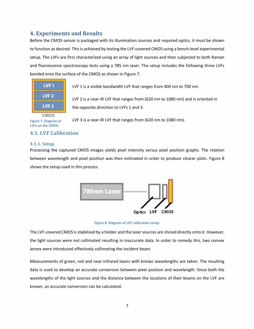
4.1.1. Setup
Processing the captured CMOS images yields pixel intensity versus pixel position graphs. The relation
between wavelength and pixel position was then estimated in order to produce clearer plots. Figure 8
shows the setup used in this process.
Figure 8. Diagram of LVF calibration setup.
The LVF-covered CMOS is stabilized by a holder and the laser sources are shined directly onto it. However,
the light sources were not collimated resulting in inaccurate data. In order to remedy this, two convex
lenses were introduced effectively collimating the incident beam.
Measurements of green, red and near-infrared lasers with known wavelengths are taken. The resulting
data is used to develop an accurate conversion between pixel position and wavelength. Since both the
wavelengths of the light sources and the distance between the locations of their beams on the LVF are
known, an accurate conversion can be calculated.
Figure 7. Diagram of LVFs on the CMOS.

8
4.1.2. Results
In order to calibrate the LVFs, two lasers of different wavelengths are shined onto the LVF-covered CMOS.
Their peaks are then compared and used in order to compute a suitable conversion function. Figures 9a
and 9b show the data obtained by shining a 633 nm red laser onto a visible bandwidth LVF. A dramatic
peak is noticed around the 2274 pixel position (pp) area, which corresponds to 633 nm. Figures 9c and 9d
show the data obtained from a 532 nm green laser. There is a similar peak at 1270 pp, which corresponds
to 532 nm.
Figure 9 a. Capture of a red 633 nm laser on LVF 1. b. 633 nm laser pixel intensity vs pixel position plot. c. Capture of a green 532 nm laser on LVF 1. d. 532 nm laser pixel intensity vs pixel position plot.
The pixel unit difference between the two peaks is calculated and compared to the wavelength distance
separating the two. The ratio between these values is the conversion constant.
𝑦𝑤𝑎𝑣𝑒𝑙𝑒𝑛𝑔𝑡ℎ = 𝑎𝑥𝑝𝑝 + 𝑏
∆𝑝𝑝 = 𝑝𝑝633 − 𝑝𝑝532 = 2274 − 1270 = 1004
∆𝜆 = 𝜆633 − 𝜆532 = 633 − 532 = 101
𝑎 =∆𝜆
∆𝑝𝑝=
101
1004
The fact that the peak positions should correspond to 532 nm and 633 nm allows for the offset to be
determined:

9
633 nm peak at 2274 pp: 633 =101
1004(2274) + 𝑏
532 nm peak at 1270 pp: 532 =101
1004(1270) + 𝑏
𝑏 = 404.241
This results in the following function:
𝑦𝑤𝑎𝑣𝑒𝑙𝑒𝑛𝑔𝑡ℎ =101
1004𝑥𝑝𝑝 + 404.421
By plugging it back into the image processor program, calibrated plots for the red and green lasers can be
obtained as shown in Figure 10.
Figure 10. 532 nm laser (green) and 633 nm lasers (red) pixel intensity vs wavelength.
Similarly, 785 nm and 808 nm lasers are used to calibrate the near-IR LVFs. Figures 11a and 11b show the
data obtained by shining a 785 nm red laser onto a near-infrared (NIR) bandwidth LVF. A dramatic peak is
noticed around the 865 pixel position (pp) area, which corresponds to 785 nm. Figures 11c and 11d show
the data obtained from an 808 nm green laser. There is a similar peak at 1040 pp, which corresponds to
808 nm.

10
Figure 11 a. Capture of a NIR 785 nm laser on LVF 2. b. 785 nm laser pixel intensity vs pixel position plot. c. Capture of a NIR 808 nm laser on LVF 2. d. 808 nm laser pixel intensity vs pixel position plot.
The pixel unit difference between the two peaks is calculated and compared to the wavelength distance
separating the two. The ratio between these values is the conversion constant.
𝑦𝑤𝑎𝑣𝑒𝑙𝑒𝑛𝑔𝑡ℎ = 𝑎𝑥𝑝𝑝 + 𝑏
∆𝑝𝑝 = 𝑝𝑝808 − 𝑝𝑝785 = 1040 − 865 = 175
∆𝜆 = 𝜆808 − 𝜆785 = 808 − 785 = 23
𝑎 =∆𝜆
∆𝑝𝑝=
23
175
The fact that the peak positions should correspond to 785 nm and 808 nm allows for the offset to be
determined:
785 nm peak at 865 pp: 785 =23
175(865) + 𝑏
808 nm peak at 1040 pp: 808 =23
175(1040) + 𝑏
𝑏 = 671.314
This results in the following function:

11
𝑦𝑤𝑎𝑣𝑒𝑙𝑒𝑛𝑔𝑡ℎ =23
175𝑥𝑝𝑝 + 671.314
By plugging it back into the image processor program, calibrated plots for the NIR lasers can be obtained
as shown in Figure 12.
Figure 12. 785 nm laser (green) and 808 nm lasers (red) pixel intensity vs wavelength.
4.2 Raman Excitation
4.2.1. Setup
Once the LVFs were calibrated, it was time to test Raman
spectroscopy. As was previously mentioned, Raman
spectroscopy consists of shining a light source onto a sample
and collecting the resulting scattered light. While most of this
light is of the same frequency as the incident light, 0.0001%
of it demonstrates frequency shifts. These shifts are
molecule-specific and allow a fingerprint to be obtained that
can be compared with known databases. For the bench
experiment, a 785 nm laser source is shined onto a sample of
Rhodamine 6G and the scattered light is collected by the
CMOS via an array of optics. The setup is detailed in Figures
13a and 13b. Since the majority of the obtained 785 nm
scattered light is useless for sample identification purposes, a notch filter is used to cutoff light around
the incident beam’s wavelength. This ideally only transmits light with Stokes and anti-Stokes frequencies.
Figure 13 a. Diagram of experimental setup. b. Picture of experimental setup.

12
4.2.2. Results
Analyzing Raman excitation data consists of
comparing the measured values to known Raman
spectral plots. In order to do this, the plots first
need to be converted into pixel intensity versus
wavenumber plots, by utilizing the wavenumber
conversion equation:
∆𝑤(𝑐𝑚−1) = (1
𝜆0−
1
𝜆1)
where 𝜆0 is the excitation wavelength (785 nm in
this case), and 𝜆1 is the Raman spectrum
wavelength.
Figures 14a and 14b show the captured image and
the resulting plot. Figure 15a shows the same plot
truncated from 200 to 2000 cm-1 in order to better compare it with the Rhodamine data in Figure 15b. It
is clearly quite difficult to discern peaks at any of the relevant frequencies. This is potentially due to a
number of factors. The noise level could be too high due to the intensity difference between the 785 nm
peak and the Raman peaks. Additionally, the notch filter might not be filtering out a sufficient percentage
of the Rayleigh scattered light. A lack of tangible results at this stage does not rule out Raman
spectroscopy. The experimental setup can still be further refined with respect to the optics and CMOS
used.
Figure 15 a. Truncated scattered light plot. b. Confirmed Rhodamine 6G spectral data [12].
Figure 14 a. Capture of scattered light from an R6G sample onto LVF2. b. Intensity versus wavenumber Raman emission plot.

13
4.3 Fluorescence
4.3.1. Setup
Fluorescence spectroscopy is performed on a sample of near-IR dye. The setup is identical to the one used
in the Raman tests. Fluorescence emission produces much higher intensity spectra than Raman excitation.
As such, clear results are to be expected.
4.3.2. Results
Figure 16 a. Capture of scattered light from an R6G sample onto LVF2. b. Intensity versus wavenumber Raman emission plot. c. NIR dye absorption/emission spectra.
Much like with Raman excitation, analyzing fluorescence data boils down to comparing obtained data to
the reported emission plots associated with the dye being used (NIR dye in this case). Figures 16a and 16b
show a sample of the gathered data. Figure 16c shows the absorption/emission spectra for near-IR dye.
The plots that were obtained show promising results. The shape associated with the emission spectra
around the 800 nm region can clearly be observed. However, some of the results show wavelength shifts
ranging from mild to very intense. This could simply be due to reflections caused by variations in the
incidence angle during the tests or inaccuracies within the CMOS itself. Most importantly, fluorescence is
observed and is resolvable using the LVF-covered CMOS.

14
5. Conclusion In its final stages, the proposed CMOS sensor package will ultimately have four light sources capable of
performing different kinds of assays. For this part of the project, only Raman and fluorescence
spectroscopy are considered due to their versatility and relative ease to test. The LVFs are first
characterized with different light sources in order to determine the wavelength to pixel position relation.
Next, Raman excitation is tested on samples of Rhodamine 6G to middling results. This is followed up by
the excitation of a near-IR fluorescent dye. The fluorescence tests are promising, producing clear, albeit
slightly shifted, emission data. It is, however, worth revisiting the Raman setup and testing different
samples. A lack of tangible results does not necessarily rule out Raman. A change in equipment and a
slight reworking of measurement methodology could potentially produce better data. Down the line,
surface-enhanced Raman spectroscopy (SERS) will be used instead of traditional Raman spectroscopy. By
exploiting the fact that Raman signals obtained from surfaces are 5 to 6 times stronger than Raman signals
from normal samples, a different version of Raman spectroscopy can be performed using lower power
illumination sources, thus making miniaturization easier [6]. SERS also produces sharper plots with less
noise, which could ultimately allow the hidden Raman peaks in our current data to be unearthed from the
noise.
Up to this point, the focus has been on putting the LVF-covered CMOS through its paces, making sure it
can resolve the specified measurement techniques on a macroscopic scale. Other diagnostic techniques
still need to be tested, notably label-free biosensor measurement, and optical absorption. In parallel to
macroscopic testing, the current device design will be scaled down in order to integrate it with a
smartphone. This involves gathering smaller optical components and illumination sources and considering
problems and challenges that inevitably come with miniaturization.

15
References
[1] Smartphone users worldwide will total 1.75 billion in 2014 - eMarketer. Retrieved April 30, 2015,
from http://www.emarketer.com/Article/Smartphone-Users-Worldwide-Will-Total-175-Billion-
2014/1010536
[2] Oncescu, V., O'dell, D., & Erickson, D. (2013). Smartphone based health accessory for colorimetric
detection of biomarkers in sweat and saliva. Lab on a Chip, 3232-3232.
[3] Tseng, D., Mudanyali, O., Oztoprak, C., Isikman, S., Sencan, I., Yaglidere, O., & Ozcan, A. (2010).
Lens-free microscopy on a cellphone. Lab on a Chip, 1787-1787.
[4] Gallegos, D., Long, K., Yu, H., Clark, P., Lin, Y., George, S., Cunningham, B. (2013). Label-free
biodetection using a smartphone. Lab on a Chip, 2124-2124.
[5] Lambrechts, A. et al. (2014) "A CMOS-compatible, integrated approach to hyper- and multispectral
imaging," Electron Devices Meeting (IEDM), 2014 IEEE International, pp. 10.5.1, 10.5.4.
[6] Introduction to CMOS image sensors. Retrieved April 30, 2015, from
http://www.olympusmicro.com/primer/digitalimaging/cmosimagesensors.html
[7] Retrieved April 30, 2015, from http://www.jdsu.com/ProductLiterature/lvf-ds-co-ae.pdf
[8] Retrieved April 30, 2015, from
http://content.piacton.com/Uploads/Princeton/Documents/Library/UpdatedLibrary/Raman_Spectr
oscopy_Basics.pdf
[9] Lakowicz, J. (1983). Principles of Fluorescence Spectroscopy. New York: Plenum Press.
[10] Guilbault, G. (1990). Practical Fluorescence (2nd ed.). New York: M. Dekker.
[11] Retrieved April 30, 2015, from http://www.turnerdesigns.com/t2/doc/appnotes/998-0050.pdf
[12] McCreery, R. (2000). Raman Spectroscopy for Chemical Analysis. New York: John Wiley & Sons.