la76810a monolithic linear ic for pal/ntsc color …dalincom.ru/datasheet/la76810a.pdf · ·...
TRANSCRIPT
N2206 MS PC B8-4814 No.A0252-1/43
■ Any and all SANYO Semiconductor products described or contained herein do not have specifications that can handle applications that require extremely high levels of reliability, such as life-support systems, aircraft’s control systems, or other applications whose failure can be reasonably expected to result in serious physical and/or material damage. Consult with your SANYO Semiconductor representative nearest you before using any SANYO Semiconductor products described or contained herein in such applications.
■ SANYO Semiconductor assumes no responsibility for equipment failures that result from using products at values that exceed, even momentarily, rated values (such as maximum ratings, operating condition ranges, or other parameters) listed in products specifications of any and all SANYO Semiconductor products described or contained herein.
LA76810A Overview
LA76810A is a VIF/SIF/Y/Deflection 1chip IC for PAL/NTSC color television sets. Functions • VIF/SIF/Y/Deflection Implemented in a 1chip. • I2C Bus Control
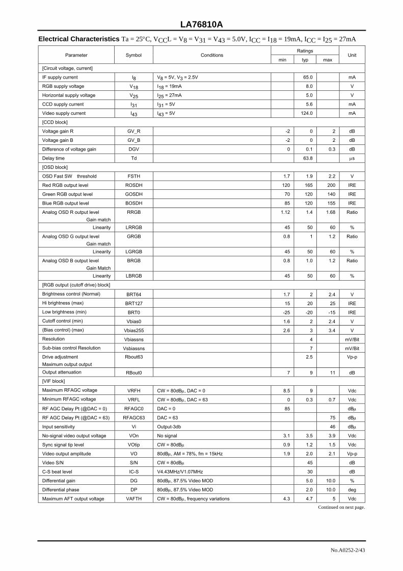
Specifications Maximum Ratings at Ta = 25°C
Parameter Symbol Conditions Ratings Unit V8 max 7.0 V
V31 max 7.0 V
Maximum supply voltage
V43 max 7.0 V
I18 max 25 mA Maximum supply current
I25 max 35 mA
Allowable power dissipation Pd max Ta ≤ 65°C * 1.6 W
Operating temperature Topg -10 to +65 °C
Storage temperature Tstg -55 to +150 °C
* Provided with a glass epoxy board (114.3×76.1×1.6 mm3)
Operating Conditions at Ta = 25°C
Parameter Symbol Conditions Ratings Unit
V8 5.0 V
V31 5.0 V
Recommended supply voltage
V43 5.0 V
I18 19 mA Recommended supply current
I25 27 mA
V8 op 4.7 to 5.3 V
V31 op 4.7 to 5.3 V
Operating supply voltage range
V43 op 4.7 to 5.3 V
I25 op 24 to 30 mA Operating supply current range
I18 op 17 to 21 mA
Monolithic Linear IC For PAL/NTSC Color Television Sets VIF/SIF/Y/Deflection 1chip IC
Ordering number : ENA0252
LA76810A
No.A0252-2/43
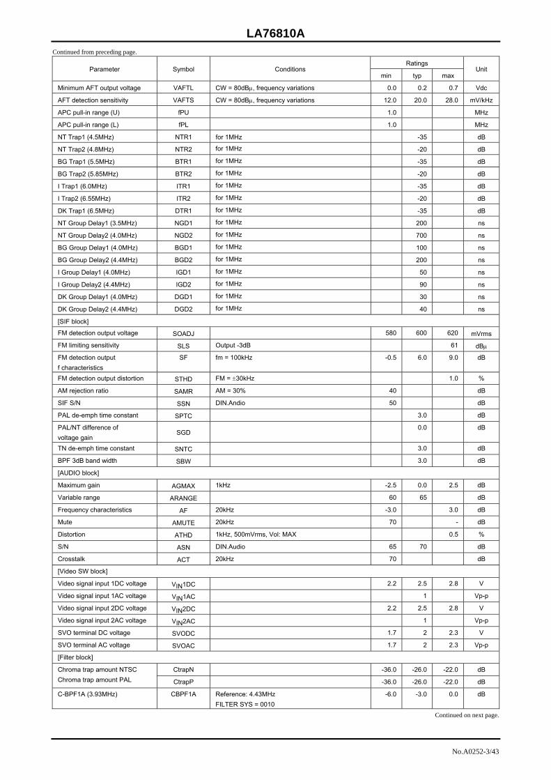
Electrical Characteristics Ta = 25°C, VCCL = V8 = V31 = V43 = 5.0V, ICC = I18 = 19mA, ICC = I25 = 27mA Ratings
Parameter Symbol Conditions min typ max
Unit
[Circuit voltage, current]
IF supply current I8 V8 = 5V, V3 = 2.5V 65.0 mA
RGB supply voltage V18 I18 = 19mA 8.0 V
Horizontal supply voltage V25 I25 = 27mA 5.0 V
CCD supply current I31 I31 = 5V 5.6 mA
Video supply current I43 I43 = 5V 124.0 mA
[CCD block]
Voltage gain R GV_R -2 0 2 dB
Voltage gain B GV_B -2 0 2 dB
Difference of voltage gain DGV 0 0.1 0.3 dB
Delay time Td 63.8 µs
[OSD block]
OSD Fast SW threshold FSTH 1.7 1.9 2.2 V
Red RGB output level ROSDH 120 165 200 IRE
Green RGB output level GOSDH 70 120 140 IRE
Blue RGB output level BOSDH 85 120 155 IRE
Analog OSD R output level Gain match
RRGB 1.12 1.4 1.68 Ratio
Linearity LRRGB 45 50 60 %
Analog OSD G output level Gain match
GRGB 0.8 1 1.2 Ratio
Linearity LGRGB 45 50 60 %
Analog OSD B output level Gain Match
BRGB 0.8 1.0 1.2 Ratio
Linearity LBRGB 45 50 60 %
[RGB output (cutoff drive) block]
Brightness control (Normal) BRT64 1.7 2 2.4 V
Hi brightness (max) BRT127 15 20 25 IRE
Low brightness (min) BRT0 -25 -20 -15 IRE
Cutoff control (min) Vbias0 1.6 2 2.4 V
(Bias control) (max) Vbias255 2.6 3 3.4 V
Resolution Vbiassns 4 mV/Bit
Sub-bias control Resolution Vsbiassns 7 mV/Bit
Drive adjustment Maximum output output
Rbout63
2.5 Vp-p
Output attenuation RBout0 7 9 11 dB
[VIF block]
Maximum RFAGC voltage VRFH CW = 80dBµ, DAC = 0 8.5 9 Vdc
Minimum RFAGC voltage VRFL CW = 80dBµ, DAC = 63 0 0.3 0.7 Vdc
RF AGC Delay Pt (@DAC = 0) RFAGC0 DAC = 0 85 dBµ
RF AGC Delay Pt (@DAC = 63) RFAGC63 DAC = 63 75 dBµ
Input sensitivity Vi Output-3db 46 dBµ
No-signal video output voltage VOn No signal 3.1 3.5 3.9 Vdc
Sync signal tip level VOtip CW = 80dBµ 0.9 1.2 1.5 Vdc
Video output amplitude VO 80dBµ, AM = 78%, fm = 15kHz 1.9 2.0 2.1 Vp-p
Video S/N S/N CW = 80dBµ 45 dB
C-S beat level IC-S V4.43MHz/V1.07MHz 30 dB
Differential gain DG 80dBµ, 87.5% Video MOD 5.0 10.0 %
Differential phase DP 80dBµ, 87.5% Video MOD 2.0 10.0 deg
Maximum AFT output voltage VAFTH CW = 80dBµ, frequency variations 4.3 4.7 5 Vdc
Continued on next page.
LA76810A
No.A0252-3/43
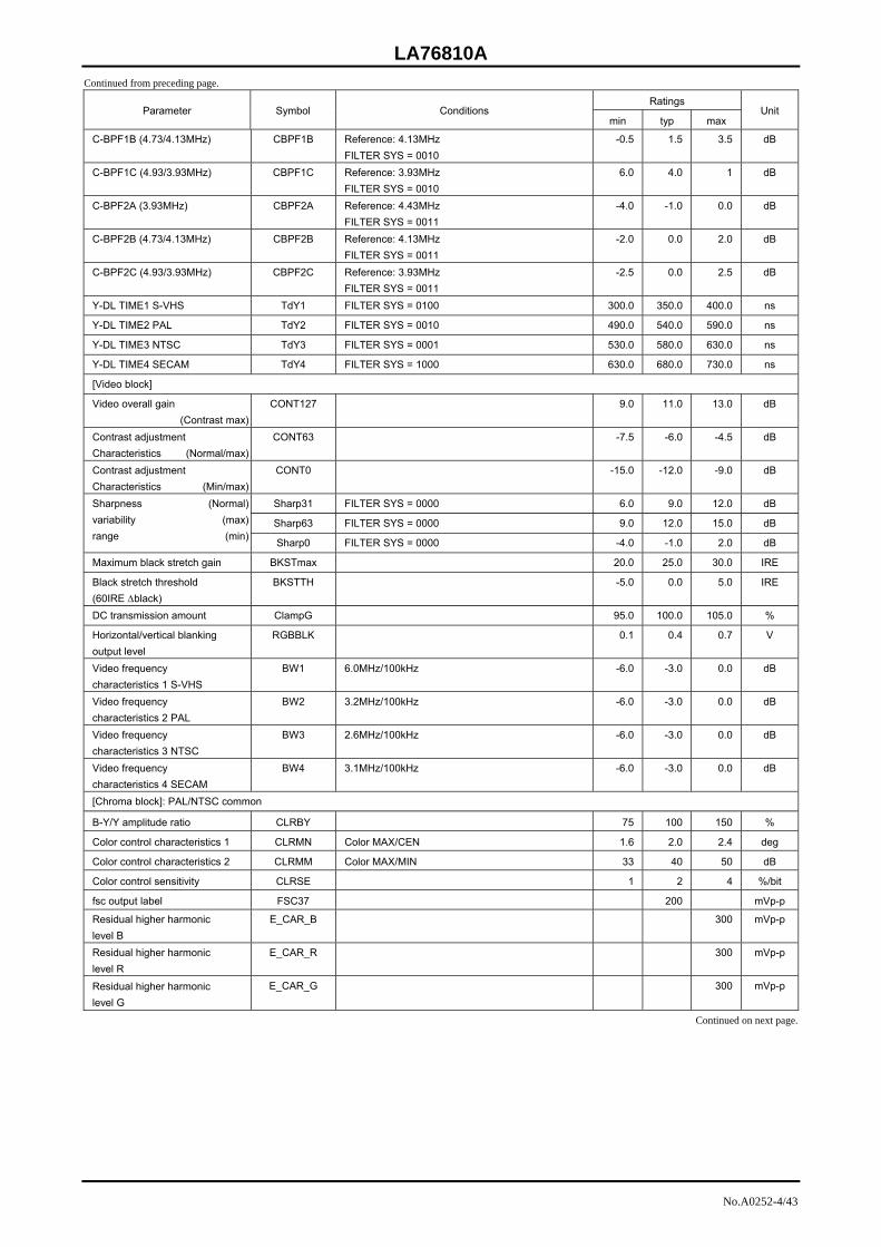
Continued from preceding page.
Ratings Parameter Symbol Conditions
min typ max Unit
Minimum AFT output voltage VAFTL CW = 80dBµ, frequency variations 0.0 0.2 0.7 Vdc
AFT detection sensitivity VAFTS CW = 80dBµ, frequency variations 12.0 20.0 28.0 mV/kHz
APC pull-in range (U) fPU 1.0 MHz
APC pull-in range (L) fPL 1.0 MHz
NT Trap1 (4.5MHz) NTR1 for 1MHz -35 dB
NT Trap2 (4.8MHz) NTR2 for 1MHz -20 dB
BG Trap1 (5.5MHz) BTR1 for 1MHz -35 dB
BG Trap2 (5.85MHz) BTR2 for 1MHz -20 dB
I Trap1 (6.0MHz) ITR1 for 1MHz -35 dB
I Trap2 (6.55MHz) ITR2 for 1MHz -20 dB
DK Trap1 (6.5MHz) DTR1 for 1MHz -35 dB
NT Group Delay1 (3.5MHz) NGD1 for 1MHz 200 ns
NT Group Delay2 (4.0MHz) NGD2 for 1MHz 700 ns
BG Group Delay1 (4.0MHz) BGD1 for 1MHz 100 ns
BG Group Delay2 (4.4MHz) BGD2 for 1MHz 200 ns
I Group Delay1 (4.0MHz) IGD1 for 1MHz 50 ns
I Group Delay2 (4.4MHz) IGD2 for 1MHz 90 ns
DK Group Delay1 (4.0MHz) DGD1 for 1MHz 30 ns
DK Group Delay2 (4.4MHz) DGD2 for 1MHz 40 ns
[SIF block]
FM detection output voltage SOADJ 580 600 620 mVrms
FM limiting sensitivity SLS Output -3dB 61 dBµ
FM detection output f characteristics
SF fm = 100kHz -0.5 6.0 9.0 dB
FM detection output distortion STHD FM = ±30kHz 1.0 %
AM rejection ratio SAMR AM = 30% 40 dB
SIF S/N SSN DIN.Andio 50 dB
PAL de-emph time constant SPTC 3.0 dB
PAL/NT difference of voltage gain
SGD 0.0 dB
TN de-emph time constant SNTC 3.0 dB
BPF 3dB band width SBW 3.0 dB
[AUDIO block]
Maximum gain AGMAX 1kHz -2.5 0.0 2.5 dB
Variable range ARANGE 60 65 dB
Frequency characteristics AF 20kHz -3.0 3.0 dB
Mute AMUTE 20kHz 70 - dB
Distortion ATHD 1kHz, 500mVrms, Vol: MAX 0.5 %
S/N ASN DIN.Audio 65 70 dB
Crosstalk ACT 20kHz 70 dB
[Video SW block]
Video signal input 1DC voltage VIN1DC 2.2 2.5 2.8 V
Video signal input 1AC voltage VIN1AC 1 Vp-p
Video signal input 2DC voltage VIN2DC 2.2 2.5 2.8 V
Video signal input 2AC voltage VIN2AC 1 Vp-p
SVO terminal DC voltage SVODC 1.7 2 2.3 V
SVO terminal AC voltage SVOAC 1.7 2 2.3 Vp-p
[Filter block]
CtrapN -36.0 -26.0 -22.0 dB Chroma trap amount NTSC Chroma trap amount PAL CtrapP -36.0 -26.0 -22.0 dB
C-BPF1A (3.93MHz) CBPF1A Reference: 4.43MHz FILTER SYS = 0010
-6.0 -3.0 0.0 dB
Continued on next page.
LA76810A
No.A0252-4/43
Continued from preceding page.
Ratings Parameter Symbol Conditions
min typ max Unit
C-BPF1B (4.73/4.13MHz) CBPF1B Reference: 4.13MHz FILTER SYS = 0010
-0.5 1.5 3.5 dB
C-BPF1C (4.93/3.93MHz) CBPF1C Reference: 3.93MHz FILTER SYS = 0010
6.0 4.0 1 dB
C-BPF2A (3.93MHz) CBPF2A Reference: 4.43MHz FILTER SYS = 0011
-4.0 -1.0 0.0 dB
C-BPF2B (4.73/4.13MHz) CBPF2B Reference: 4.13MHz FILTER SYS = 0011
-2.0 0.0 2.0 dB
C-BPF2C (4.93/3.93MHz) CBPF2C Reference: 3.93MHz FILTER SYS = 0011
-2.5 0.0 2.5 dB
Y-DL TIME1 S-VHS TdY1 FILTER SYS = 0100 300.0 350.0 400.0 ns
Y-DL TIME2 PAL TdY2 FILTER SYS = 0010 490.0 540.0 590.0 ns
Y-DL TIME3 NTSC TdY3 FILTER SYS = 0001 530.0 580.0 630.0 ns
Y-DL TIME4 SECAM TdY4 FILTER SYS = 1000 630.0 680.0 730.0 ns
[Video block]
Video overall gain (Contrast max)
CONT127 9.0 11.0 13.0 dB
Contrast adjustment Characteristics (Normal/max)
CONT63 -7.5 -6.0 -4.5 dB
Contrast adjustment Characteristics (Min/max)
CONT0 -15.0 -12.0 -9.0 dB
Sharp31 FILTER SYS = 0000 6.0 9.0 12.0 dB
Sharp63 FILTER SYS = 0000 9.0 12.0 15.0 dB
Sharpness (Normal) variability (max) range (min) Sharp0 FILTER SYS = 0000 -4.0 -1.0 2.0 dB
Maximum black stretch gain BKSTmax 20.0 25.0 30.0 IRE
Black stretch threshold (60IRE ∆black)
BKSTTH -5.0 0.0 5.0 IRE
DC transmission amount ClampG 95.0 100.0 105.0 %
Horizontal/vertical blanking output level
RGBBLK 0.1 0.4 0.7 V
Video frequency characteristics 1 S-VHS
BW1 6.0MHz/100kHz -6.0 -3.0 0.0 dB
Video frequency characteristics 2 PAL
BW2 3.2MHz/100kHz -6.0 -3.0 0.0 dB
Video frequency characteristics 3 NTSC
BW3 2.6MHz/100kHz -6.0 -3.0 0.0 dB
Video frequency characteristics 4 SECAM
BW4 3.1MHz/100kHz -6.0 -3.0 0.0 dB
[Chroma block]: PAL/NTSC common
B-Y/Y amplitude ratio CLRBY 75 100 150 %
Color control characteristics 1 CLRMN Color MAX/CEN 1.6 2.0 2.4 deg
Color control characteristics 2 CLRMM Color MAX/MIN 33 40 50 dB
Color control sensitivity CLRSE 1 2 4 %/bit
fsc output label FSC37 200 mVp-p
Residual higher harmonic level B
E_CAR_B
300 mVp-p
Residual higher harmonic level R
E_CAR_R
300 mVp-p
Residual higher harmonic level G
E_CAR_G
300 mVp-p
Continued on next page.
LA76810A
No.A0252-5/43
Continued from preceding page.
Ratings Parameter Symbol Conditions
min typ max Unit
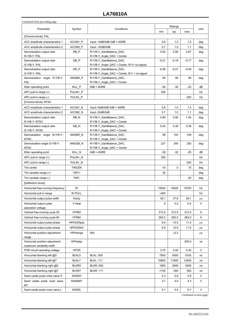
[Chroma block]: PAL
ACC amplitude characteristics 1 ACCM1_P Input: +6dB/0dB 0dB = 40IRE 0.8 1.0 1.2 deg
ACC amplitude characteristics 2 ACCM2_P Input: -20dB/0dB 0.7 1.0 1.1 deg
Demodulation output ratio R-Y/B-Y: PAL
RB_P R-Y/B-Y_GainBalance_DAC, R-Y/B-Y_Angle_DAC = Center
0.50 0.56 0.67 deg
Demodulation output ratio G-Y/B-Y: PAL
GB_P R-Y/B-Y_GainBalance_DAC, R-Y/B-Y_Angle_DAC = Center, R-Y= no-signal
-0.21 -0.19 -0.17 deg
Demodulation output ratio G-Y/R-Y: PAL
GR_P R-Y/B-Y_GainBalance_DAC, R-Y/B-Y_Angle_DAC = Center, B-Y = no-signal
-0.56 -0.51 -0.46 deg
Demodulation angle R-Y/B-Y: PAL
ANGBR_P R-Y/B-Y_GainBalance_DAC, R-Y/B-Y_Angle_DAC = Center
85 90 95 deg
Killer operating point KILL_P 0dB = 40IRE -36 -30 -23 dB
APC pull-in range (+) PULIN+_P 350 Hz
APC pull-in range (-) PULIN-_P -350 Hz
[Chroma block]: NTSC
ACC amplitude characteristics 1 ACCM1_N Input:+6dB/0dB 0dB = 40IRE 0.8 1.0 1.2 deg
ACC amplitude characteristics 2 ACCM2_N Input:-20dB/0dB 0.7 1.0 1.1 deg
Demodulation output ratio R-Y/B-Y: NTSC
RB_N R-Y/B-Y_GainBalance_DAC, R-Y/B-Y_Angle_DAC = Center
0.80 0.90 1.00 deg
Demodulation output ratio G-Y/B-Y: NTSC
GB_N R-Y/B-Y_GainBalance_DAC, R-Y/B-Y_Angle_DAC = Center
0.24 0.30 0.38 deg
Demodulation angle B-Y/R-Y: NTSC
ANGBR_N R-Y/B-Y_GainBalance_DAC, R-Y/B-Y_Angle_DAC = Center
99 104 109 deg
Demodulation angle G-Y/B-Y: NTSC
ANGGB_N R-Y/B-Y_GainBalance_DAC, R-Y/B-Y_Angle_DAC = Center
227 240 250 deg
Killer operating point KILL_N 0dB = 40IRE -39 -32 -25 dB
APC pull-in range (+) PULIN+_N 350 Hz
APC pull-in range (-) PULIN-_N -350 Hz
Tint center TINCEN -10 0 10 deg
Tint variable range (+) TINT+ 35 deg
Tint variable range (-) TINT- -35 deg
[Deflection block]
Horizontal free-running frequency fH 15500 15625 15750 Hz
Horizontal pull-in range fH PULL ±400 Hz
Horizontal output pulse width Hduty 36.1 37.6 39.1 µs
Horizontal output pulse saturation voltage
V Hsat 0 0.2 0.4 V
Vertical free-running cycle 50 VFR50 312.0 312.5 313.0 H
Vertical free-running cycle 60 VFR60 262.0 262.5 263.0 H
Horizontal output pulse phase HPHCENpal 9.5 10.5 11.5 µs
Horizontal output pulse phase HPHCENnt 9.5 10.5 11.5 µs
Horizontal position adjustment range
HPHrange 5bit ±2.2 µs
Horizontal position adjustment maximum variability width
HPHstep 200.0 ns
POR circuit operating voltage VPOR 3.70 4.00 4.30 V
Horizontal blanking left @0 BLKL0 BLKL: 000 7500 8300 9100 ns
Horizontal blanking left @7 BLKL7 BLKL: 111 10800 11600 12400 ns
Horizontal blanking right @0 BLKR0 BLKR: 000 1800 2600 3400 ns
Horizontal blanking right @7 BLKR7 BLKR: 111 -1100 -300 500 ns
Sand castle pulse crest value H SANDH 5.3 5.6 5.9 V
Sand castle pulse crest value M1
SANDM1 3.7 4.0 4.3 V
Sand castle pulse crest value L SANDL 0.1 0.4 0.7 V
Continued on next page.
LA76810A
No.A0252-6/43
Continued from preceding page.
Ratings Parameter Symbol Conditions
min typ max Unit
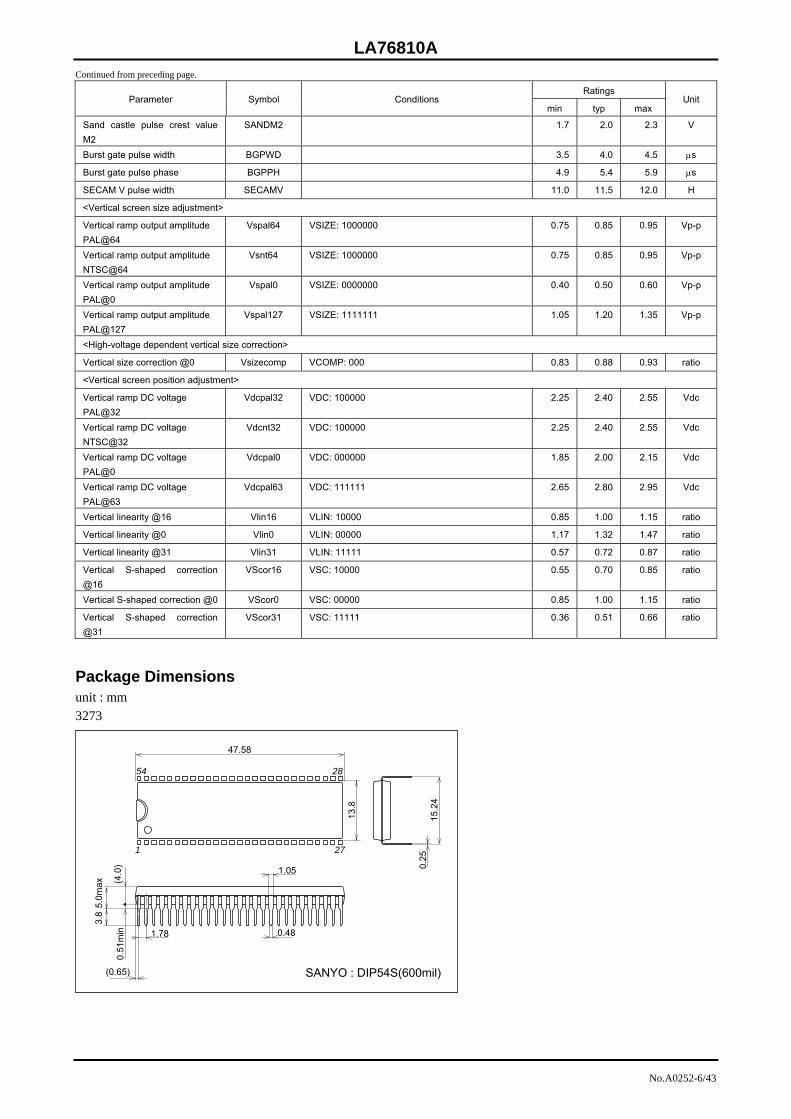
Sand castle pulse crest value M2
SANDM2 1.7 2.0 2.3 V
Burst gate pulse width BGPWD 3.5 4.0 4.5 µs
Burst gate pulse phase BGPPH 4.9 5.4 5.9 µs
SECAM V pulse width SECAMV 11.0 11.5 12.0 H
<Vertical screen size adjustment>
Vertical ramp output amplitude PAL@64
Vspal64 VSIZE: 1000000 0.75 0.85 0.95 Vp-p
Vertical ramp output amplitude NTSC@64
Vsnt64 VSIZE: 1000000 0.75 0.85 0.95 Vp-p
Vertical ramp output amplitude PAL@0
Vspal0 VSIZE: 0000000 0.40 0.50 0.60 Vp-p
Vertical ramp output amplitude PAL@127
Vspal127 VSIZE: 1111111 1.05 1.20 1.35 Vp-p
<High-voltage dependent vertical size correction>
Vertical size correction @0 Vsizecomp VCOMP: 000 0.83 0.88 0.93 ratio
<Vertical screen position adjustment>
Vertical ramp DC voltage PAL@32
Vdcpal32 VDC: 100000 2.25 2.40 2.55 Vdc
Vertical ramp DC voltage NTSC@32
Vdcnt32 VDC: 100000 2.25 2.40 2.55 Vdc
Vertical ramp DC voltage PAL@0
Vdcpal0 VDC: 000000 1.85 2.00 2.15 Vdc
Vertical ramp DC voltage PAL@63
Vdcpal63 VDC: 111111 2.65 2.80 2.95 Vdc
Vertical linearity @16 Vlin16 VLIN: 10000 0.85 1.00 1.15 ratio
Vertical linearity @0 Vlin0 VLIN: 00000 1.17 1.32 1.47 ratio
Vertical linearity @31 Vlin31 VLIN: 11111 0.57 0.72 0.87 ratio
Vertical S-shaped correction @16
VScor16 VSC: 10000 0.55 0.70 0.85 ratio
Vertical S-shaped correction @0 VScor0 VSC: 00000 0.85 1.00 1.15 ratio
Vertical S-shaped correction @31
VScor31 VSC: 11111 0.36 0.51 0.66 ratio
Package Dimensions unit : mm 3273
SANYO : DIP54S(600mil)
47.58
13.8
1.05
0.48
(0.65)
1.78
(4.0
)
3.8
5.0m
ax
0.51
min
15.2
40.
25
1 27
54 28
LA76810A
No.A0252-7/43
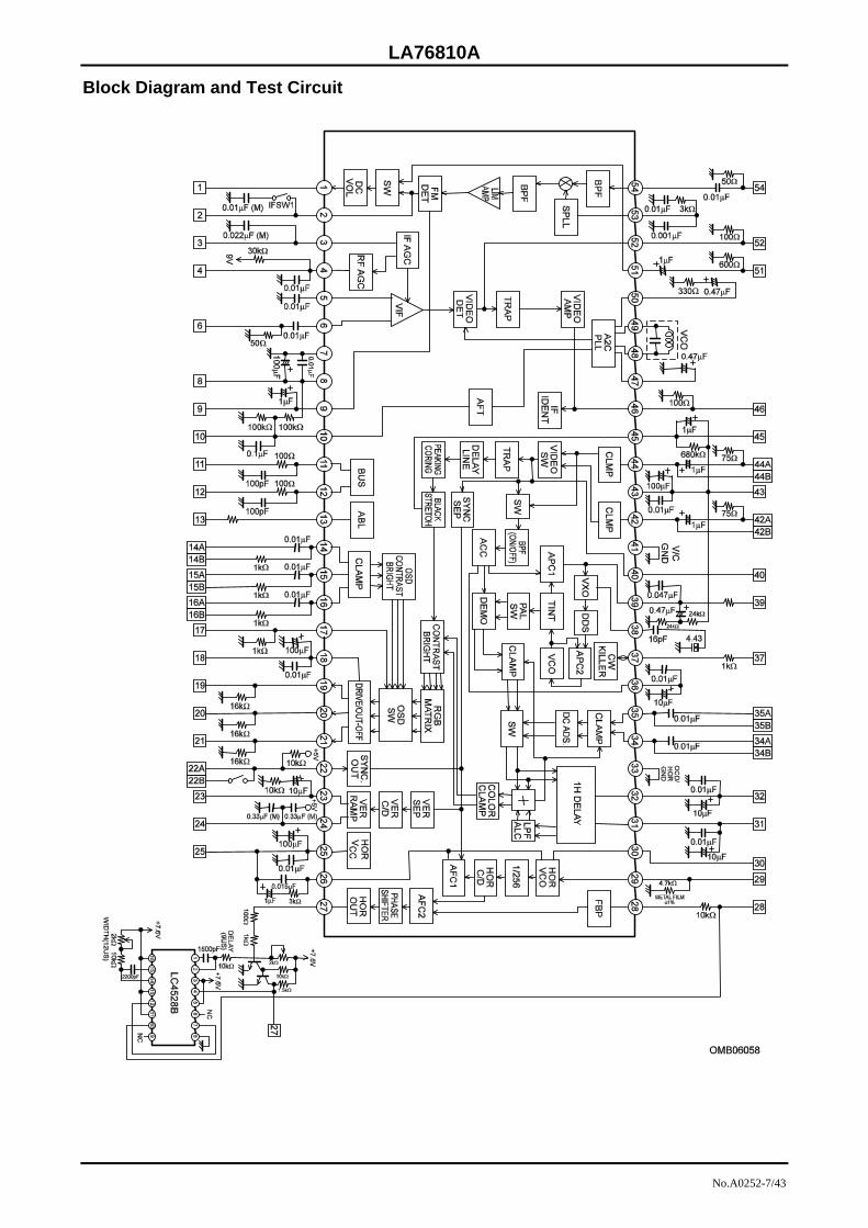
Block Diagram and Test Circuit
LA76810A
NoA0252-8/40
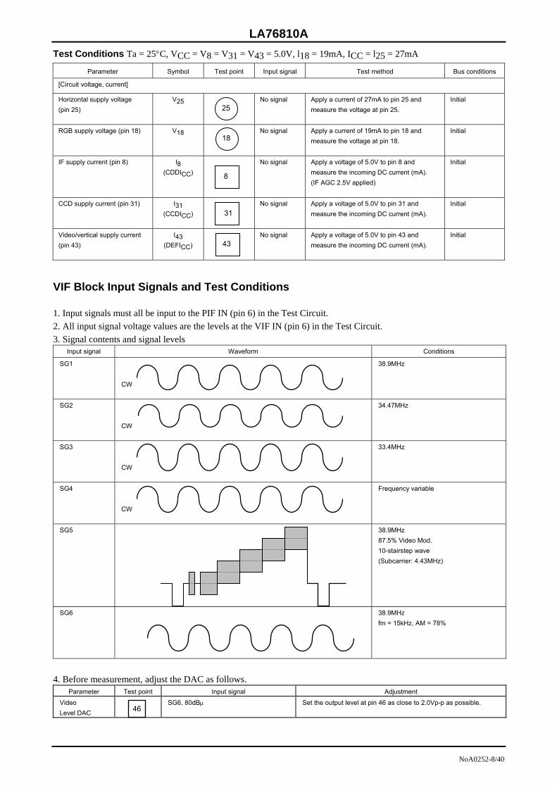
Test Conditions Ta = 25°C, VCC = V8 = V31 = V43 = 5.0V, l18 = 19mA, ICC = l25 = 27mA
Parameter Symbol Test point Input signal Test method Bus conditions
[Circuit voltage, current]
Horizontal supply voltage (pin 25)
V25 No signal Apply a current of 27mA to pin 25 and measure the voltage at pin 25.
Initial
RGB supply voltage (pin 18) V18 No signal Apply a current of 19mA to pin 18 and measure the voltage at pin 18.
Initial
IF supply current (pin 8) I8 (CDDICC)
No signal Apply a voltage of 5.0V to pin 8 and measure the incoming DC current (mA). (IF AGC 2.5V applied)
Initial
CCD supply current (pin 31) I31 (CCDICC)
No signal Apply a voltage of 5.0V to pin 31 and measure the incoming DC current (mA).
Initial
Video/vertical supply current (pin 43)
I43 (DEFICC)
No signal Apply a voltage of 5.0V to pin 43 and measure the incoming DC current (mA).
Initial
VIF Block Input Signals and Test Conditions 1. Input signals must all be input to the PIF IN (pin 6) in the Test Circuit. 2. All input signal voltage values are the levels at the VIF IN (pin 6) in the Test Circuit. 3. Signal contents and signal levels
Input signal Waveform Conditions
SG1 CW
38.9MHz
SG2 CW
34.47MHz
SG3 CW
33.4MHz
SG4 CW
Frequency variable
SG5
38.9MHz 87.5% Video Mod. 10-stairstep wave (Subcarrier: 4.43MHz)
SG6
38.9MHz fm = 15kHz, AM = 78%
4. Before measurement, adjust the DAC as follows.
Parameter Test point Input signal Adjustment
Video Level DAC
SG6, 80dBµ Set the output level at pin 46 as close to 2.0Vp-p as possible.
25
18
8
43
31
46
LA76810A
NoA0252-9/40
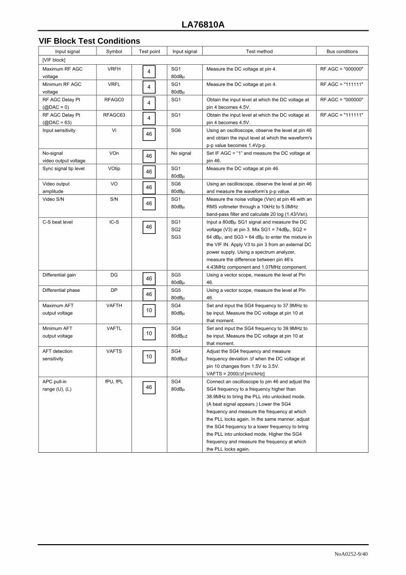
VIF Block Test Conditions Input signal Symbol Test point Input signal Test method Bus conditions
[VIF block]
Maximum RF AGC voltage
VRFH SG1 80dBµ
Measure the DC voltage at pin 4. RF.AGC = "000000"
Minimum RF AGC voltage
VRFL SG1 80dBµ
Measure the DC voltage at pin 4. RF.AGC = "111111"
RF AGC Delay Pt (@DAC = 0)
RFAGC0 SG1 Obtain the input level at which the DC voltage at pin 4 becomes 4.5V.
RF.AGC = "000000"
RF AGC Delay Pt (@DAC = 63)
RFAGC63 SG1
Obtain the input level at which the DC voltage at pin 4 becomes 4.5V.
RF.AGC = "111111"
Input sensitivity Vi SG6
Using an oscilloscope, observe the level at pin 46 and obtain the input level at which the waveform's p-p value becomes 1.4Vp-p.
No-signal video output voltage
VOn No signal Set IF AGC = “1” and measure the DC voltage at pin 46.
Sync signal tip level VOtip SG1 80dBµ
Measure the DC voltage at pin 46.
Video output amplitude
VO SG6 80dBµ
Using an oscilloscope, observe the level at pin 46 and measure the waveform’s p-p value.
Video S/N S/N SG1 80dBµ
Measure the noise voltage (Vsn) at pin 46 with an RMS voltmeter through a 10kHz to 5.0MHz band-pass filter and calculate 20 log (1.43/Vsn).
C-S beat level IC-S SG1 SG2 SG3
Input a 80dBµ SG1 signal and measure the DC voltage (V3) at pin 3. Mix SG1 = 74dBµ, SG2 = 64 dBµ, and SG3 = 64 dBµ to enter the mixture in the VIF IN. Apply V3 to pin 3 from an external DC power supply. Using a spectrum analyzer, measure the difference between pin 46’s 4.43MHz component and 1.07MHz component.
Differential gain DG SG5 80dBµ
Using a vector scope, measure the level at Pin 46.
Differential phase DP SG5 80dBµ
Using a vector scope, measure the level at Pin 46.
Maximum AFT output voltage
VAFTH SG4 80dBµ
Set and input the SG4 frequency to 37.9MHz to be input. Measure the DC voltage at pin 10 at that moment.
Minimum AFT output voltage
VAFTL SG4 80dBµz
Set and input the SG4 frequency to 39.9MHz to be input. Measure the DC voltage at pin 10 at that moment.
AFT detection sensitivity
VAFTS SG4 80dBµz
Adjust the SG4 frequency and measure frequency deviation ∆f when the DC voltage at pin 10 changes from 1.5V to 3.5V. VAFTS = 2000/∆f [mV/kHz]
APC pull-in range (U), (L)
fPU, fPL SG4 80dBµ
Connect an oscilloscope to pin 46 and adjust the SG4 frequency to a frequency higher than 38.9MHz to bring the PLL into unlocked mode. (A beat signal appears.) Lower the SG4 frequency and measure the frequency at which the PLL locks again. In the same manner, adjust the SG4 frequency to a lower frequency to bring the PLL into unlocked mode. Higher the SG4 frequency and measure the frequency at which the PLL locks again.
4
4
4
4
46
46
46
46
46
46
46
10
46
46
10
10
LA76810A
NoA0252-10/40
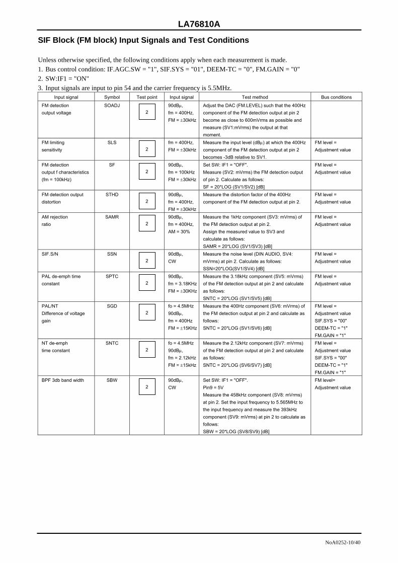
SIF Block (FM block) Input Signals and Test Conditions
Unless otherwise specified, the following conditions apply when each measurement is made. 1. Bus control condition: IF.AGC.SW = "1", SIF.SYS = "01", DEEM-TC = "0", FM.GAIN = "0" 2. SW:IF1 = "ON" 3. Input signals are input to pin 54 and the carrier frequency is 5.5MHz.
Input signal Symbol Test point Input signal Test method Bus conditions
FM detection output voltage
SOADJ 2
90dBµ, fm = 400Hz,FM = ±30kHz
Adjust the DAC (FM.LEVEL) such that the 400Hz component of the FM detection output at pin 2 become as close to 600mVrms as possible and measure (SV1:mVrms) the output at that moment.
FM limiting sensitivity
SLS 2
fm = 400Hz,FM = ±30kHz
Measure the input level (dBµ) at which the 400Hz component of the FM detection output at pin 2 becomes -3dB relative to SV1.
FM level = Adjustment value
FM detection output f characteristics (fm = 100kHz)
SF 2
90dBµ, fm = 100kHzFM = ±30kHz
Set SW: IF1 = "OFF". Measure (SV2: mVrms) the FM detection output of pin 2. Calculate as follows: SF = 20*LOG (SV1/SV2) [dB]
FM level = Adjustment value
FM detection output distortion
STHD 2
90dBµ, fm = 400Hz,FM = ±30kHz
Measure the distortion factor of the 400Hz component of the FM detection output at pin 2.
FM level = Adjustment value
AM rejection ratio
SAMR 2
90dBµ, fm = 400Hz,AM = 30%
Measure the 1kHz component (SV3: mVrms) of the FM detection output at pin 2. Assign the measured value to SV3 and calculate as follows: SAMR = 20*LOG (SV1/SV3) [dB]
FM level = Adjustment value
SIF.S/N SSN 2
90dBµ, CW
Measure the noise level (DIN AUDIO, SV4: mVrms) at pin 2. Calculate as follows: SSN=20*LOG(SV1/SV4) [dB]
FM level = Adjustment value
PAL de-emph time constant
SPTC 2
90dBµ, fm = 3.18KHzFM = ±30KHz
Measure the 3.18kHz component (SV5: mVrms) of the FM detection output at pin 2 and calculate as follows: SNTC = 20*LOG (SV1/SV5) [dB]
FM level = Adjustment value
PAL/NT Difference of voltage gain
SGD 2
fo = 4.5MHz90dBµ, fm = 400Hz FM = ±15KHz
Measure the 400Hz component (SV6: mVrms) of the FM detection output at pin 2 and calculate as follows: SNTC = 20*LOG (SV1/SV6) [dB]
FM level = Adjustment value SIF.SYS = "00" DEEM-TC = "1" FM.GAIN = "1"
NT de-emph time constant
SNTC 2
fo = 4.5MHz90dBµ, fm = 2.12kHzFM = ±15kHz
Measure the 2.12kHz component (SV7: mVrms) of the FM detection output at pin 2 and calculate as follows: SNTC = 20*LOG (SV6/SV7) [dB]
FM level = Adjustment value SIF.SYS = "00" DEEM-TC = "1" FM.GAIN = "1"
BPF 3db band width SBW 2
90dBµ, CW
Set SW: IF1 = "OFF". Pin9 = 5V Measure the 458kHz component (SV8: mVrms) at pin 2. Set the input frequency to 5.565MHz to the input frequency and measure the 393kHz component (SV9: mVrms) at pin 2 to calculate as follows: SBW = 20*LOG (SV8/SV9) [dB]
FM level= Adjustment value
LA76810A
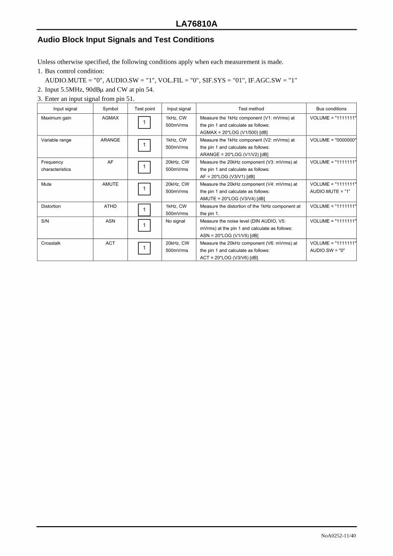
NoA0252-11/40
Audio Block Input Signals and Test Conditions Unless otherwise specified, the following conditions apply when each measurement is made. 1. Bus control condition:
AUDIO.MUTE = "0", AUDIO.SW = "1", VOL.FIL = "0", SIF.SYS = "01", IF.AGC.SW = "1" 2. Input 5.5MHz, 90dBµ and CW at pin 54. 3. Enter an input signal from pin 51.
Input signal Symbol Test point Input signal Test method Bus conditions
Maximum gain AGMAX 1kHz, CW 500mVrms
Measure the 1kHz component (V1: mVrms) at the pin 1 and calculate as follows: AGMAX = 20*LOG (V1/500) [dB]
VOLUME = "1111111"
Variable range ARANGE 1kHz, CW 500mVrms
Measure the 1kHz component (V2: mVrms) at the pin 1 and calculate as follows: ARANGE = 20*LOG (V1/V2) [dB]
VOLUME = "0000000"
Frequency characteristics
AF 20kHz, CW 500mVrms
Measure the 20kHz component (V3: mVrms) at the pin 1 and calculate as follows: AF = 20*LOG (V3/V1) [dB]
VOLUME = "1111111"
Mute AMUTE 20kHz, CW 500mVrms
Measure the 20kHz component (V4: mVrms) at the pin 1 and calculate as follows: AMUTE = 20*LOG (V3/V4) [dB]
VOLUME = "1111111"AUDIO.MUTE = ”1”
Distortion ATHD 1kHz, CW 500mVrms
Measure the distortion of the 1kHz component at the pin 1.
VOLUME = "1111111"
S/N ASN No signal Measure the noise level (DIN AUDIO, V5: mVrms) at the pin 1 and calculate as follows: ASN = 20*LOG (V1/V5) [dB]
VOLUME = "1111111"
Crosstalk ACT 20kHz, CW 500mVrms
Measure the 20kHz component (V6: mVrms) at the pin 1 and calculate as follows: ACT = 20*LOG (V3/V6) [dB]
VOLUME = "1111111"AUDIO.SW = "0"
1
1
1
1
1
1
1
LA76810A
NoA0252-12/40
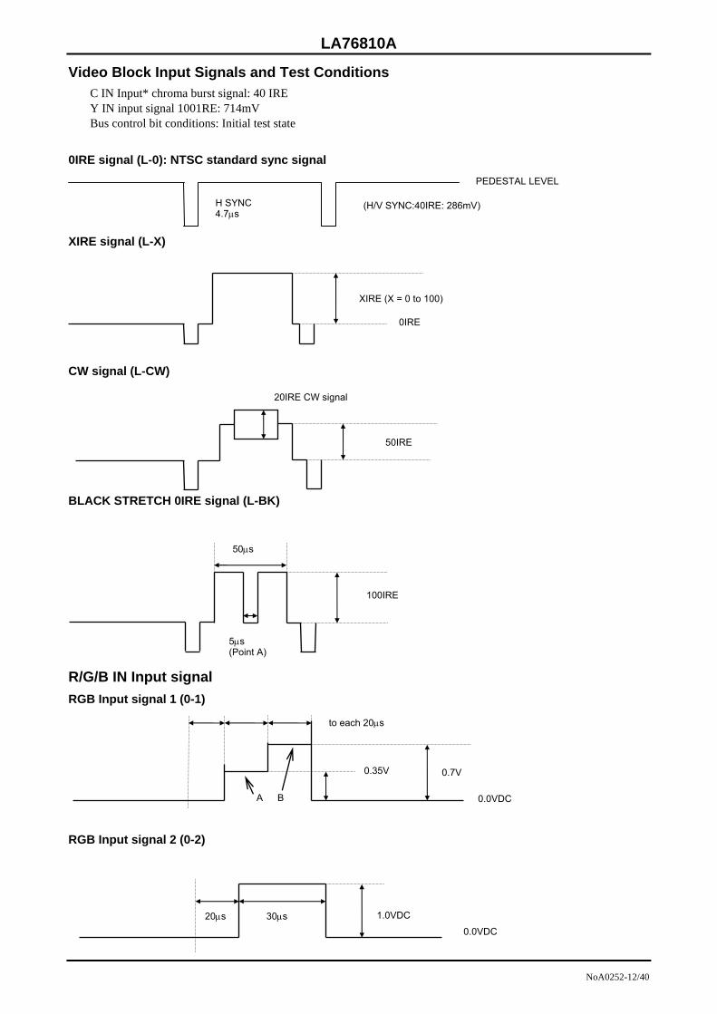
Video Block Input Signals and Test Conditions C IN Input* chroma burst signal: 40 IRE Y IN input signal 1001RE: 714mV Bus control bit conditions: Initial test state
0IRE signal (L-0): NTSC standard sync signal XIRE signal (L-X)
CW signal (L-CW)
BLACK STRETCH 0IRE signal (L-BK)
R/G/B IN Input signal RGB Input signal 1 (0-1)
RGB Input signal 2 (0-2)
PEDESTAL LEVEL
H SYNC 4.7µs
(H/V SYNC:40IRE: 286mV)
XIRE (X = 0 to 100)
0IRE
20IRE CW signal
50IRE
50µs
100IRE
5µs (Point A)
to each 20µs
0.35V 0.7V
0.0VDC A B
20µs 30µs 1.0VDC
0.0VDC

LA76810A
NoA0252-13/40
Video Block Test Conditions Input signal Symbol Test point Input signal Test method Bus bit/input signal
Video overall gain (Contrast max)
CONT127 L-50 Measure the output signal’s 50IRE amplitude (CNTHB Vp-p) and calculate CONT127 = 20Log (CNTHB/0.357).
CONTRAST: 1111111
Contrast adjustment characteristics (normal/max)
CONT63 L-50 Measure the output signal’s 50IRE amplitude (CNTCB Vp-p) and calculate CONT63 = 20Log (CNTCB/0.357).
CONTRAST: 0111111
Contrast adjustment characteristics (min/max)
CONT0 L-50 Measure the output signal’s 50IRE amplitude (CNTLB Vp-p) and calculate CONT0 = 20Log (CNTLB/0.357).
CONTRAST: 0000000
Video frequency Characteristics 1 (SVHS)
BW1 L-CW
With the input signal’s continuous wave = 100kHz, measure the output signal’s continuous wave amplitude (PEAKDC Vp-p). With the input signal’s continuous wave = 6MHz, measure the output signal’s continuous wave amplitude (CW7 Vp-p). Calculate BW1 = 20Log (CW6/PEAKDC).
FILTER SYS: 0100 SHARPNESS: 000000
Video frequency Characteristics 2 (PAL)
BW2 L-CW With the input signal’s continuous wave = 3.2MHz, measure the output signal’s continuous wave amplitude (CW3.2 Vp-p). Calculate BW2 = 20Log (CW3.2/PEAKDC).
FILTER SYS: 0010 SHARPNESS: 000000
Video frequency Characteristics 3 (NTSC)
BW3 L-CW
With the input signal’s continuous wave = 2.6MHz, measure the output signal’s continuous wave amplitude (CW2.6 Vp-p). Calculate BW3 = 20Log (CW2.6/PEAKDC).
FILTER SYS: 0000 SHARPNESS: 000000
Video frequency Characteristics 4 (SECAM)
BW4 L-CW With the input signal’s continuous wave = 3.1MHz, measure the output signal’s continuous wave amplitude (CW3.1 Vp-p). Calculate BW4 = 20Log (CW3.1/PEAKDC).
FILTER SYS: 1000 SHARPNESS: 000000
With the input signal’s continuous wave = 4.43MHz, measure the output signal’s continuous wave amplitude (F0P Vp-p).
FILTER SYS: 010 Sharpness: 000000
Chroma trap amount PAL
CtraPP L-CW
Calculate CtraP = 20Log (F0P/PEAKDC).
With the input signal’s continuous wave = 3.58MHz, measure the output signal’s continuous wave amplitude (F0N Vp-p).
FILTER SYS: 000 Sharpness: 000000
Chroma trap amount NTSC
CtraPN L-CW
Calculate CtraN = 20Log (F0N/PEAKDC).
L-0 Measure the output signal’s 0IRE DC level (BRTPL V).
Brightness: 0000000 CONTRAST: 1111111
DC transmission amount
ClampG1
L-100 Measure the output signal’s 0IRE DC level (DRVPH V) and 100IRE amplitude (DRVH Vp-p) and calculate ClampG = 100 × (1+(DRVPH - BRTPL)/DRVH).
Brightness: 0000000 Contrast: 1111111
Y-DL TIME1(SVHS) TdY1 L-50 Obtain the time difference (the delay time) from when the rise of the input signal's 50IRE amplitude to the output signal's 50IRE amplitude.
FILTER SYS:0100
Y-DL TIME2(PAL) TdY2 L-50 Obtain the time difference (the delay time) from when the rise of the input signal's 50IRE amplitude to the output signal's 50IRE amplitude.
FILTER SYS:0010
Y-DL TIME3(NTSC) TdY3 L-50 Obtain the time difference (the delay time) from when the rise of the input signal's 50IRE amplitude to the output signal's 50IRE amplitude.
FILTER SYS:0000
Y-DL TIME4(SECAM) TdY4 L-50 Obtain the time difference (the delay time) from when the rise of the input signal's 50IRE amplitude to the output signal's 50IRE amplitude.
FILTER SYS:1000
Continued on next page.
21
21
21
21
21
21
21
21
21
21
21
21
21
21
LA76810A
NoA0252-14/40
Continued from preceding page.
Input signal Symbol Test point Input signal Test method Bus bit/input signal
Measure the 0IRE DC level (BKST1 V) at point A of the output signal in the Black Stretch Defeat (Black Stretch OFF) mode.
Measure the 0IRE DC level (BKST2 V) at point A of the output signal in the Black Stretch ON mode.
Blk Str DEF: 0
Maximum black stretch gain
BKSTmax L-BK
Calculate BKSTmax=2×50× (BKST1-BKST2) /CNTHB.
Measure the 60IRE DC level (BKST3 V) of the output signal in the Black Stretch Defeat ON mode.
Blk Str DEF: 0
Measure the 60IRE DC level (BKST4 V) of the output signal in the Black Stretch Defeat (Black Stretch OFF) mode.
Black stretch threshold ∆black (60IRE ∆black)
BKSTTH∆ L-60
Calculate BKSTTH∆ = 50× (BKST4-BKST3)/CNTHB.
Sharpness variability characteristics
With the input signal’s continuous wave = 2.2MHz, measure the output signal’s continuous wave amplitude (F00S31 Vp-p).
FILTER SYS:0000 Sharpness: 100000
(normal)
Sharp31 L-CW
Calculate Sharp31 = 20Log (F00S31/PEAKDC).
With the input signal’s continuous wave = 2.2MHz, measure the output signal’s continuous wave amplitude (F00S63 Vp-p).
FILTER SYS:0000 Sharpness: 111111
(max) Sharp63 L-CW
Calculate Sharp63=20Log (F00S63/PEAKDC).
With the input signal’s continuous wave=2.2MHz, measure the output signal’s continuous wave amplitude (F00S0 Vp-p).
FILTER SYS:0000 Sharpness: 000000
(min) Sharp0
L-CW
Calculate Sharp0 = 20Log (F00S0/PEAKDC).
Horizontal/vertical blanking output level
RGBBLK L-100 Measure the DC level (RGBBLK V) for the output signal’s blanking period.
[OSD block] Bus control bit conditions: Contrast = 63, Brightness = 63 Input signal Symbol Test point Input signal Test method Bus bit/input signal
OSD Fast SW threshold
FSTH L-0 O-2
Apply voltage to pin 17 and measure the voltage at pin 17 at the point where the output signal switches to the OSD signal.
Pin 16A: O-2 applied
L-50 Measure the output signal’s 50IRE amplitude (CNTCR Vp-p).
L-0 O-2
Measure the OSD output amplitude (OSDHR Vp-p).
Pin 17: 3.5V Pin 14A: O-2 applied
Red RGB output level
ROSDC
Calculate ROSDC = 50 × (ROSDC /CNTCR) L-50 Measure the output signal’s 50IRE amplitude
(CNTCG Vp-p).
L-0 O-2
Measure the OSD output amplitude (OSDHG Vp-p).
Pin 17: 3.5V Pin 15A: O-2 applied
Green RGB output level
GOSDC
Calculate GOSDC = 50 × (GOSDC/CNTCG)
Continued on next page.
21
21
21
21
21
19
20

LA76810A
NoA0252-15/40
Continued from preceding page.
Input signal Symbol Test point Input signal Test method Bus bit/input signal
L-50 Measure the output signal’s 50IRE amplitude (CNTCB Vp-p).
L-0 O-2
Measure the OSD output amplitude (OSDHB Vp-p).
Pin 17: 3.5V Pin 16A: O-2 applied
Blue RGB output level
BOSDC
Calculate BOSDC = 50 × (OSDHB/CNTCB)
Analog OSD R output level
L-0 O-1
Measure the amplitudes at point A (0.35V portion of the input signal 0-1) and point B (0.7V portion of the input signal 0-1) of the output signal. Assign the measured values to RGBLR Vp-p and RGBHR Vp-p, respectively.
Pin 17 : 3.5V Pin 14A : O-1 applied
Gain match RRGB Calculate RRGB = RGBLR/CNTCR.
linearity LRRGB Calculate LRRGB = 100 × (RGBLR/RGBHR).
Analog OSD G output level
L-0 O-1
Measure the amplitudes at point A (0.35V portion of the input signal 0-1) and point B (0.7V portion of the input signal 0-1) of the output signal. Assign the measured values to RGBLG Vp-p and RGBHG Vp-p, respectively.
Pin 17: 3.5V Pin 15A: O-1 applied
Gain match GRGB Calculate GRGB = RGBLG/CNTCG.
linearity LGRGB Calculate LGRGB = 100 × (RGBLG/RGBHG).
Analog OSD B output level
L-0 O-1
Measure the amplitudes at point A (0.35V portion of the input signal 0-1) and point B (0.7V portion of the input signal 0-1) of the output signal. Assign the measured values to RGBLB Vp-p and RGBHB Vp-p, respectively.
Pin 17: 3.5V Pin 16A: O-1 applied
Gain・match BRGB Calculate BRGB = RGBLB/CNTCB.
linearity LBRGB Calculate LBRGB = 100 × (RGBLB/RGBHB).
.
[RGB output block] (Cutoff, drive block) Bus control bit conditions: Contrast=127 Input signal Symbol Test point Input signal Test method Bus bit/input signal
Measure the 0IRE DC levels of the respective output signals of R output (19), G output (20), and B output (21). Assign the measured values to BRTPCR, BRTPCG, and BRTPCB V, respectively.
Brightness: 01111111
Brightness control (normal)
BRT63
L-0
Calculate BRT63 = (BRTPCR+BRTPCG+ BRTPCB)/3.
Measure the 0IRE DC level of the output signal of B output (21) and assign the measured value to BRTPHB.
Brightness: 1111111
(max) BRT127
Calculate BRT127 = 50 × (BRTPHB-BRTPCB)/ CNTHB.
Measure the 0IRE DC level of the output signal of B output (21) and assign the measured value to BRTPLB.
Brightness: 0000000
(min) BRT0
Calculate BRT0 = 50 × (BRTPLB-BRTPCB)/ CNTHB.
Continued on next page.
20
19
21
21
20
19
21
21
LA76810A
NoA0252-16/40
Continued from preceding page.
Input signal Symbol Test point Input signal Test method Bus bit/input signal
Bias (cutoff) control (min)
Vbias0 L-50 Measure the 0IRE DC levels (Vbias0* V) of the respective output signals of R output (19), G output (20), and B output (21). *: R, G, and B
Sub-Brightness: 0000000
(max)
Vbias255 Measure the 0IRE DC levels (Vbias255* V) of the respective output signals of R output (19), G output (20), and B output (21). *: R, G, and B
Sub-Brightness: 1111111 Red/Green/Blue Bias: 11111111
Measure the 0IRE DC levels (BAS80* V) of the respective output signals of R output (19), G output (20), and B output (21). *: R, G, and B
Red/Green/Blue Bias:01010000
Measure the 0IRE DC levels (BAS48* V) of the respective output signals of R output (19), G output (20), and B output (21).
Red/Green/Blue Bias: 00110000
Bias (cutoff) control resolution
Vbiassns
Calculate Vbiassns* = (BAS80*-BAS48*)/32
Measure the 0IRE DC levels (SBTPM* V) of the respective output signals of R output (19), G output (20), and B output (21).
Sub-Brightness: 0101010 Contrast: 0111111
Sub-bias control resolution
Vsbiassns L-50
Calculate Vsbiassns* = (BRTPC*-SBTPM*)
Drive adjustment maximum output
RBout127
Gout15
L-100 Measure the 100IRE amplitudes (DRVH* Vp-p) of the respective output signals of R output (19) and B output (21). *: R and B Measure the 100IRE amplitude of the output signal of G output (20) and assign the measured value to DRVH* Vp-p. *: G
Brightness: 0000000
Output attenuation RBout0 Measure the 100IRE amplitudes (DRVL* Vp-p) of the respective output signals of R output (19), G output (20), and B output (21). *: R and B Measure the 100IRE amplitude of the output signal of G output (20) and assign the measured value to DRVL* Vp-p. *: G
Brightness: 0000000 Red/Blue Drive: 0000000
Gout0
RBout0* = 20Log (DRVH*/DRVL*) Gout0* = 20Log (DRVH*/DRVL*)
Measure the 100IRE amplitude of the respective output signals of R output (28), G output (29), and B output (30) with Gamma Def being ON and OFF. Assign the measured values to *A, *B and Vp-p, respectively. * : R, G, B
Contrast: 0111111 Brightness: 01111111 Gamma Def: Off,OnB Gamma sel: 11,00
Gamma correction
Rγ Gγ Bγ
L-100
*γ = 100*(*A/*B)
20
19
21
20
19
21
20
19
21

LA76810A
NoA0252-17/40
[VIDEO SW block] Bus control bit conditions: Contrast = 63, Brightness = 63 Input signal Symbol Test point Input signal Test method Bus bit/input signal
Video signal input 1DC voltage
VIN1DC
L-100 Input signals to pin 42 and measure the voltage of the pedestal.
VIDEO SW: 1
Video signal input 2DC voltage
VIN2DC
L-100 Input signals to pin 44 and measure the voltage of the pedestal.
VIDEO SW: 0
SVO terminal DC voltage
SVODC
L-100 Input signals to pin 42 and measure the voltage of the pedestal at pin 40.
VIDEO SW: 1
SVO terminal AC voltage
SVOAC
L-100 Input signals to pin 42 and measure the voltage of the pedestal at pin 40.
VIDE0 SW: 1
Chroma Block Input Signals and Test Conditions Unless otherwise specified, the following conditions apply when each measurement is made. 1. VIF, SIF blocks: No signal 2. Deflection Block: Horizontal/vertical composite sync signals are input and the deflection block must be locked into
the sync signals (Refer to the Deflection Block Input Signals and the Test Conditions). 3. Bus control conditions: Set the following conditions unless otherwise specified.
Y Input is 42 Pin (EXT-V IN), C Input is 44 Pin (S-C IN) (Video SW=1, C.Ext=1)
Other DAC except the above-mentioned conditions is all initial conditions. 4. Y Input condition: No signal unless otherwise specified.
(Sync is necessary to obtain synchronization). 5. How to calculate the demodulation ratio and angle:
B-Y axis angle = tan-1(B(0)/B(270))+270° R-Y axis angle = tan-1(R(180)/R( 90))+90° G-Y axis angle = tan-1(G(270)/G(180))+180°
B-Y axis amplitude Vb = SQRT(B(0)*B(0)+B(270)*B(270)) R-Y axis amplitude Vr = SQRT(R(180)*R(180)+R(90)*R(90)) G-Y axis amplitude Vg = SQRT(G(180)*G(180)+G(270)*G(270))
90°
180°
270°
0°
B(0)
R(90)
G(270)
R(180)
G(180)
B(270)
R-Y axis
B-Y axis
G-Y axis
42
44
40
40
LA76810A
NoA0252-18/40
6. Chroma input signal: As for the PAL signal, the burst swings such as 130° and 225° every one hour. Chroma describes the phase caused when the burst occurs at 135°. As for the NTSC signal, the burst occurs constantly at 180°. The figures below are based on the phase of NTSC. When a PAL signal is generated, adjust the phase and then enter signals. The item common to both PAL and NTSC is the PAL signal. For those other than this, the measurement must be performed for each individual signals. The condition of fsc: Set the following conditions unless otherwise specified. PAL = 4.433619MHz NTSC = 3.579545MHz C-1 X IRE signal (L-X) C-2 C-3 C-4 C-5
Burst 0° 90° 180° 270° fsc
40IRE
Burst fsc 346°
40IRE 62.5IRE
Burst fsc CW (Note: fsc±N*fh when the frequency is specified.
N should be a natural number and the nearest value should be used.)
Burst B-Y only
Burst R-Y only
40IRE
LA76810A
NoA0252-19/40
[Chroma block]: PAL/NTSC common Input signal Symbol Test point Input signal Test method Bus bit/input signal
YIN:L77 No signal
Measure the Y system’s output level. V1
B-Y/Y amplitude ratio
CLRBY
Bout
21 C-2 Input a signal to the CIN (only sync signal to the YIN) and measure the output level to calculate as follows: CLRBY = 100 × (V2/V1)+15%
Color: 1000000
Color control characteristics 1
CLRMN 21
C-1 Measure the output amplitude V1 at color control MAX mode and output amplitude V2 at color control CEN mode and, calculate as follows: CLRMN = V1/V2
Color: 1111111 Color: 1000000
Color control Characteristics 2
CLRMM 21
C-1 Measure the output amplitude V3 at color control MIN mode to calculate as follows: CLRMM = 20log (V1/V3)
Color: 0000000
Color control sensitivity
CLRSE 21
C-1 Measure the output amplitude V4 at color control 90 mode and output amplitude V5 at color control 38 mode to calculate as follows: CLRSE = 100 × (V4-V5)/(V2×52)
Color: 1011010 Color: 0100110
fsc output level FSC37 37
Measure 4.43MHz output amplitude at pin 37.
Residual higher harmonic level B
E_CAR_B 21
C-1 Burst only
Measure the 8.86MHz component output amplitude at pin 21.
Residual higher harmonic level R
E_CAR_R Rout
21
Burst only Measure the 8.86MHz component output amplitude at pin 19.
Residual higher harmonic level G
E_CAR_G Gout
21
C-1 Burst only
Measure the 8.86MHz component output amplitude at pin 20.
[Chroma block]: PAL Input signal Symbol Test point Input signal Test method Bus bit/input signal
ACC amplitude characteristics 1
ACCM1_P Bout
21
C-1 0dB +6dB
Measure the output amplitude when 0dB is applied to the chroma input and the output amplitude when +6dB is applied to the chroma input and calculate the ratio between them. ACCM1 = 20LOG (+6dBdata/0dBdata)
Color: 1000000
ACC amplitude characteristics 2
ACCM2_P Bout
21
C-1 -20dB
Measure the output amplitude when –20dB is applied to the chroma input and calculate the ratio between them. ACCM2 = 20LOG (-20dBdata/0dBdata)
Color: 1000000
Demodulation output ratio R-Y/B-Y: PAL
RB_P 21
19
C-1 Refer to 5. and measure Bout output amplitude Vb and ROUT output amplitude Vr. And calculate RB = Vr/Vb.
Color: 1000000
Demodulation output ratio G-Y/B-Y: PAL
GB_P 21
19
C-4 Measure Bout output amplitude Vbp and GOUT output amplitude Vgbp. And calculate GB_P = Vgb-p/Vb-p.
Color: 1000000
Continued on next page.

LA76810A
NoA0252-20/40
Continued from preceding page.
Input signal Symbol Test point Input signal Test method Bus bit/input signal
Demodulation output ratio G-Y/R-Y: PAL
GR_P 20
19
C-5 Measure Rout output amplitude Vrp and GOUT output amplitude Vgbp. And calculate GR_P = Vgrp/Vrp.
Color: 1000000
Demodulation angle B-Y/R-Y: PAL
ANGBR_P 21
19
C-1 Refer to 5. and measure the B-Y and R-Y demodulation angle and calculate.
Color: 1000000
APC pull-in range (+) PULIN+_P 21
C-1 Decrease the chroma fsc frequency from 4.433619MHz+1000Hz and measure the frequency at which the VCO locks.
APC pull-in range (-) PULIN-_P 21
C-1 Increase the chroma fsc frequency from 4.433619MHz-1000Hz and measure the frequency at which the VCO locks.
[Chroma block]: NTSC Input signal Symbol Test point Input signal Test method Bus bit/input signal
ACC amplitude characteristics 1
ACCM1_N Bout
21
C-1 0dB +6dB
Measure the output amplitude when 0dB is applied to the chroma input and the output amplitude when +6dB is applied to the chroma input and calculate the ratio between them. ACCM1 = 20LOG (+6dBdata/0dBdata)
ACC amplitude characteristics 2
ACCM2_N Bout
21
C-1 -20dB
Measure the output amplitude when 20dB is applied to the chroma input and calculate the ratio between them. ACCM2 = 20LOG (-20dBdata/0dBdata)
R-Y/B-Y: NTSC Demodulation output ratio R-Y/B-Y: NTSC
RB_N 21
19
C-1 Refer to 5. and measure Bout output amplitude Vb and ROUT output amplitude Vr. And calculate RB = Vr/Vb.
Color: 1000000
G-Y/B-Y: NTSC Demodulation output ratio R-Y/B-Y: NTSC
GB_N 20
C-1 Refer to 5. and measure GOUT output amplitude Vg. And calculate GB_N = Vg/Vb.
Color: 1000000
Demodulation angle B-Y/R-Y: NTSC
ANGBR_N 21
19
C-1 Refer to 5. and measure the B-Y and R-Y demodulation angle and calculate. Reference: B-Y angle
Color: 1000000
Demodulation angle G-Y/B-Y: NTSC
ANGGB_N 21
20
C-1 Refer to 5. and measure the B-Y and G-Y demodulation angle and calculate. Reference: B-Y angle
Color: 1000000
Killer operating point
KILL_N 21
C-1 Reduce the input signal until the output level becomes 150mVp-p or less. Measure the input level at that moment.
APC pull-in range (+) PULIN+_N 21
C-1 Decrease the chroma fsc frequency from 3.579545MHz+1000Hz and measure the frequency at which the VCO locks.
APC pull-in range (-) PULIN-_N 21
C-1 Increase the chroma fsc frequency from 3.579545MHz-1000Hz and measure the frequency at which the VCO locks.
Tint center TINCEN 21
C-1 Measure each part of the output level and calculate the B-Y axis angle.
TINT: 1000000
Continued on next page.

LA76810A
NoA0252-21/40
Continued from preceding page.
Input signal Symbol Test point Input signal Test method Bus bit/input signal
Tint variable range (+) TINT+ 21
C-1 Measure each part of the output level and calculate the B-Y axis angle. TINT+ = B-Y axis angle -TINCEN
TINT 1111111
Tint variable range (-) TINT- 21
C-1 Measure each part of the output level and calculate the B-Y axis angle. TINT- = B-Y axis angle -TINCEN
TINT 0000000
[Filter Block Chroma BPF Characteristic]
Input signal Symbol Test point Input signal Test method Bus bit/input signal
C-BPF1A Peaker amplitude characteristic 3.93MHz
CBPF1A 21
C-3 PAL signal
Set the chroma frequency (CW) to 4.433619MHz-100kHz and measure V0 output amplitude. And then, set the chroma frequency (CW) to 3.93MHz and measure V1 output amplitude to calculate as follows: CBPF1A = 20LOG (V1/V0)
FILTER SYS = 0010C.BYPASS = 0
C-BPF1B Peaker amplitude characteristic 4.73/4.13MHz
CBPF1B 21
C-3 PAL signal
Measure V2 output amplitude when the chroma frequency (CW) is 4.13MHz and V3 output amplitude when it (CW) is 4.73MHz to calculate as follows: CBPF1B = 20LOG (V3/V2)
FILTER SYS = 0010C.BYPASS = 0
C-BPF1C Peaker amplitude characteristic 4.93/3.93MHz
CBPF1C 21
C-3 PAL signal
Set the chroma frequency (CW) to 4.93MHz and measure V4 output amplitude to calculate as follows: CBPF1C = 20LOG (V4/V1)
FILTER SYS = 0010C.BYPASS = 0
C-BPF2A BandPass amplitude characteristic 3.93MHz
CBPF2A 21
C-3 PAL signal
Set the chroma frequency (CW) to 4.433619MHz-100MHz and measure V00 output amplitude. And then, set the chroma frequency (CW) to 3.93MHz and measure V10 output amplitude to calculate as follows: CBPF2A = 20LOG (V10/V00)
FILTER SYS = 0011C.BYPASS = 0
C-BPF2B BandPass amplitude characteristic 4.73/4.13MHz
CBPF2B 21
C-3 PAL signal
Measure V20 output amplitude when the chroma frequency (CW) is 4.13MHz and V30 output amplitude when it (CW) is 4.73MHz to calculate as follows: CBPF2B = 20LOG (V30/V20)
FILTER SYS = 0011C.BYPASS = 0
C-BPF2C BandPass amplitude characteristic 4.93/3.93MHz
CBPF2C 21
C-3 PAL signal
Set the chroma frequency (CW) to 4.93MHz and measure V40 output amplitude to calculate as follows: CBPF2C = 20LOG (V40/V10)
FILTER SYS = 0011C.BYPASS = 0
LA76810A
NoA0252-22/40
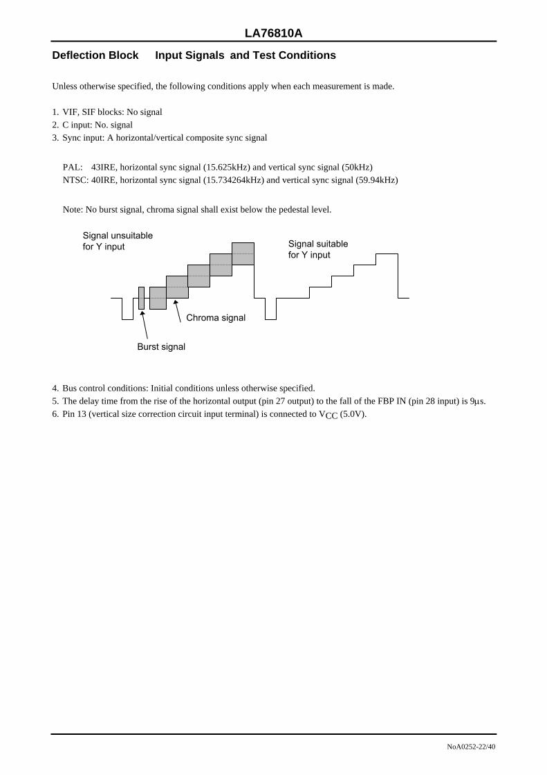
Deflection Block Input Signals and Test Conditions Unless otherwise specified, the following conditions apply when each measurement is made. 1. VIF, SIF blocks: No signal 2. C input: No. signal 3. Sync input: A horizontal/vertical composite sync signal
PAL: 43IRE, horizontal sync signal (15.625kHz) and vertical sync signal (50kHz) NTSC: 40IRE, horizontal sync signal (15.734264kHz) and vertical sync signal (59.94kHz)
Note: No burst signal, chroma signal shall exist below the pedestal level.
4. Bus control conditions: Initial conditions unless otherwise specified. 5. The delay time from the rise of the horizontal output (pin 27 output) to the fall of the FBP IN (pin 28 input) is 9µs. 6. Pin 13 (vertical size correction circuit input terminal) is connected to VCC (5.0V).
Burst signal
Chroma signal
Signal unsuitable for Y input Signal suitable
for Y input
LA76810A
NoA0252-23/40
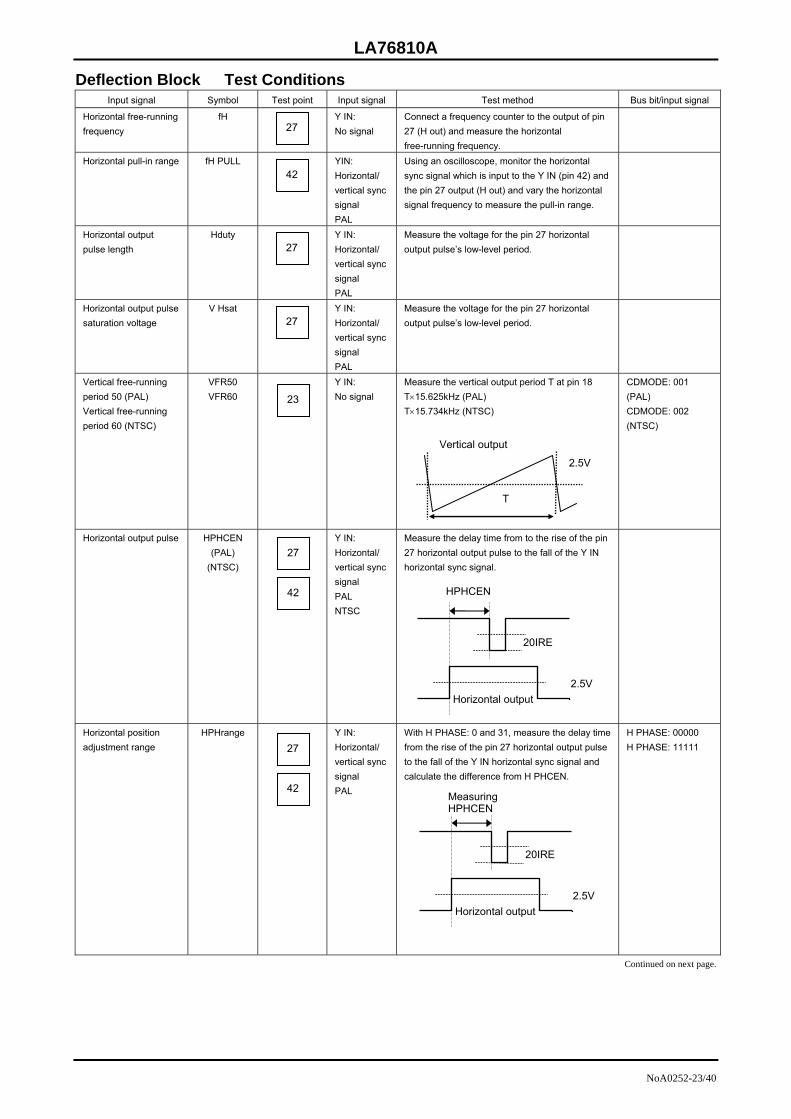
Deflection Block Test Conditions Input signal Symbol Test point Input signal Test method Bus bit/input signal
Horizontal free-running frequency
fH Y IN: No signal
Connect a frequency counter to the output of pin 27 (H out) and measure the horizontal free-running frequency.
Horizontal pull-in range fH PULL YIN: Horizontal/ vertical sync signal PAL
Using an oscilloscope, monitor the horizontal sync signal which is input to the Y IN (pin 42) and the pin 27 output (H out) and vary the horizontal signal frequency to measure the pull-in range.
Horizontal output pulse length
Hduty Y IN: Horizontal/ vertical sync signal PAL
Measure the voltage for the pin 27 horizontal output pulse’s low-level period.
Horizontal output pulse saturation voltage
V Hsat Y IN: Horizontal/ vertical sync signal PAL
Measure the voltage for the pin 27 horizontal output pulse’s low-level period.
Vertical free-running period 50 (PAL) Vertical free-running period 60 (NTSC)
VFR50 VFR60
Y IN: No signal
Measure the vertical output period T at pin 18 T×15.625kHz (PAL) T×15.734kHz (NTSC)
CDMODE: 001 (PAL) CDMODE: 002 (NTSC)
Horizontal output pulse
HPHCEN (PAL)
(NTSC)
Y IN: Horizontal/ vertical sync signal PAL NTSC
Measure the delay time from to the rise of the pin 27 horizontal output pulse to the fall of the Y IN horizontal sync signal.
Horizontal position adjustment range
HPHrange Y IN: Horizontal/ vertical sync signal PAL
With H PHASE: 0 and 31, measure the delay time from the rise of the pin 27 horizontal output pulse to the fall of the Y IN horizontal sync signal and calculate the difference from H PHCEN.
H PHASE: 00000 H PHASE: 11111
Continued on next page.
27
42
27
27
23
42
27
42
27
HPHCEN
20IRE
2.5V Horizontal output
T
2.5V
Vertical output
Measuring HPHCEN
20IRE
2.5V Horizontal output
LA76810A
NoA0252-24/40
Continued from preceding page.
Input signal Symbol Test point Input signal Test method Bus bit/input signal
Horizontal position adjustment maximum variable width
HPHstep Y IN: Horizontal/ vertical sync signal PAL
With H PHASE: 0 to 31 varied, measure the delay time from to the rise of the pin 27 horizontal output pulse to the fall of the Y IN horizontal sync signal and calculate the variation at each step. Retrieve data for maximum variation.
H PHASE: 00000 to H PHASE: 11111
POR circuit operating voltage
VPOR Y IN: Horizontal/ vertical sync signal PAL
Connect a DC power supply in place of the current source to pin 25 and gradually decrease the voltage from 5.0V until the BUS READ TATUS [POR][STATUS1 (DA01) becomes "1". Measure the DC voltage at pin 25 at the moment.
Horizontal blanking left variable range@0
BLKL0 Y IN: Horizontal/ vertical sync signal PAL
Measure the time T from the left end of Hsync at pin 42 Y IN to the left end of blanking at pin 21 BlueOUT with BLKL = 000.
BLKL: 000
Horizontal blanking left variable range@7
BLKL7 Y IN: Horizontal/ vertical sync signal PAL
Measure the time T from the left end of Hsync at pin 42 Y IN to the left end of blanking at pin 21 BlueOUT with BLKL = 111.
BLKL: 111
Continued on next page.
MeasuringHPHCEN
20IRE
Horizontal output
42
27
Blue
Hsync Y IN T
Blue
Hsync Y IN T
42
21
25
42
21

LA76810A
NoA0252-25/40
Continued from preceding page.
Input signal Symbol Test point Input signal Test method Bus bit/input signal
Horizontal blanking right variable range@0
BLKR0 Y IN: Horizontal/ vertical sync signal PAL
Measure the time T from the left end of Hsync at pin 42 Y IN to the left end of blanking at pin 21 BlueOUT with BLKR = 000.
BLKR: 000
Horizontal blanking right variable range@7
BLKR7 Y IN: Horizontal/ vertical sync signal PAL
Measure the time T from the left end of Hsync at pin 42 Y IN to the left end of blanking at pin 21 BlueOUT with BLKR = 111.
BLKR: 111
Sand castle pulse crest value H
SANDH Y IN: Horizontal/ vertical sync signal PAL
Measure the supply voltage at point H of the pin 28 FBP IN wave form for Hsync period.
Sand castle pulse crest value M1
SANDM1 Y IN: Horizontal/ vertical sync signal PAL
Measure the supply voltage at point M1 of the pin 28 FBP IN wave form for Hsync period.
Sand castle pulse crest value L
SANDL Y IN: Horizontal/ vertical sync signal PAL
Measure the supply voltage at point L of the pin 28 FBP IN wave form for Hsync period.
Sand castle pulse crest value M2
SANDM2 Y IN: Horizontal/ vertical sync signal PAL
Measure the supply voltage at point M2 of the pin 28 FBP IN wave form for Vsync period.
Burst gate pulse length BGPWD Y IN: Horizontal/ vertical sync signal PAL
Measure the BGP width T of the pin 28 FBP IN wave form for Hsync period.
Continued on next page.
28
28
28
28
42
21
42
21
Blue
Hsync Y IN T
Blue
Hsync Y IN T
H
M1
L
L
28
T
LA76810A
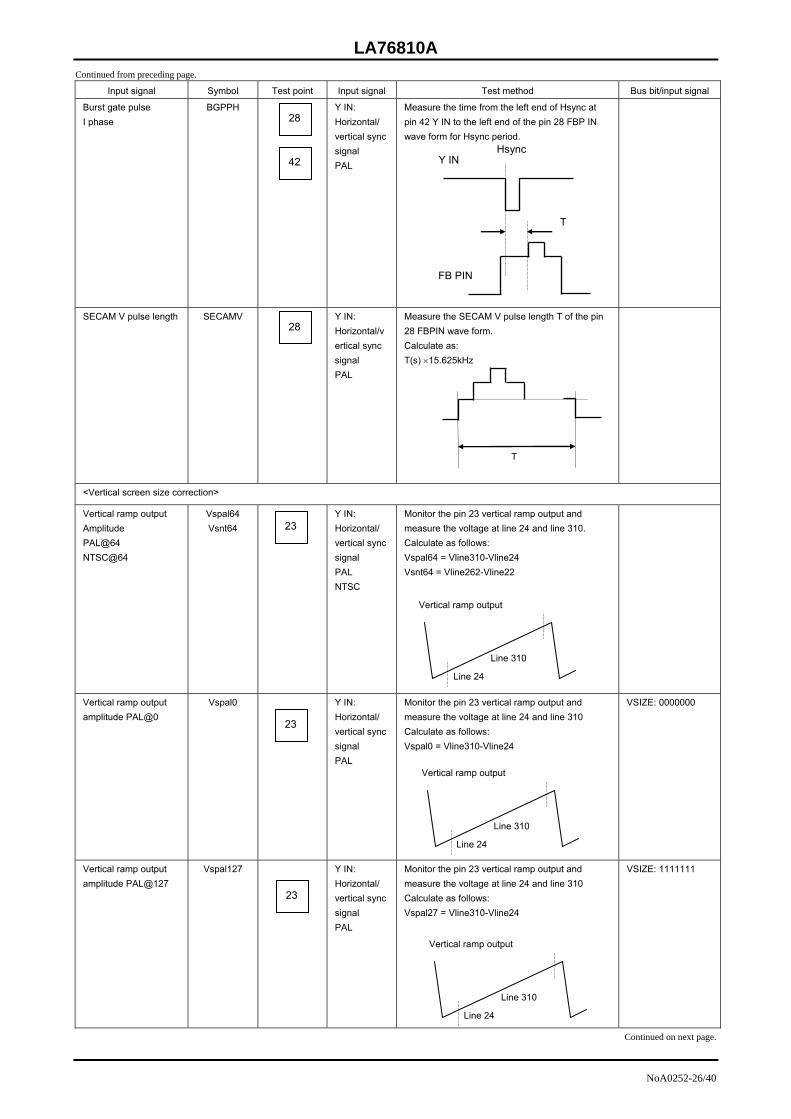
NoA0252-26/40
Continued from preceding page.
Input signal Symbol Test point Input signal Test method Bus bit/input signal
Burst gate pulse I phase
BGPPH Y IN: Horizontal/ vertical sync signal PAL
Measure the time from the left end of Hsync at pin 42 Y IN to the left end of the pin 28 FBP IN wave form for Hsync period.
SECAM V pulse length SECAMV Y IN: Horizontal/vertical sync signal PAL
Measure the SECAM V pulse length T of the pin 28 FBPIN wave form. Calculate as: T(s) ×15.625kHz
<Vertical screen size correction>
Vertical ramp output Amplitude PAL@64 NTSC@64
Vspal64 Vsnt64
Y IN: Horizontal/ vertical sync signal PAL NTSC
Monitor the pin 23 vertical ramp output and measure the voltage at line 24 and line 310. Calculate as follows: Vspal64 = Vline310-Vline24 Vsnt64 = Vline262-Vline22
Vertical ramp output amplitude PAL@0
Vspal0 Y IN: Horizontal/ vertical sync signal PAL
Monitor the pin 23 vertical ramp output and measure the voltage at line 24 and line 310 Calculate as follows: Vspal0 = Vline310-Vline24
VSIZE: 0000000
Vertical ramp output amplitude PAL@127
Vspal127
Y IN: Horizontal/ vertical sync signal PAL
Monitor the pin 23 vertical ramp output and measure the voltage at line 24 and line 310 Calculate as follows: Vspal27 = Vline310-Vline24
VSIZE: 1111111
Continued on next page.
42
28
Y IN Hsync
FB PIN
T
T
28
Line 310
Line 24
Vertical ramp output
Line 310
Line 24
Vertical ramp output
Line 310
Line 24
Vertical ramp output
23
23
23
LA76810A
NoA0252-27/40
Continued from preceding page.
Input signal Symbol Test point Input signal Test method Bus bit/input signal
<High-voltage dependent vertical size correction>
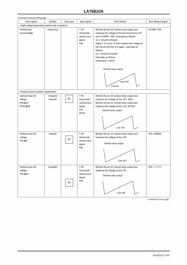
Vertical size correction@0
Vsizecomp Y IN: Horizontal/ vertical sync signal PAL
Monitor the pin 23 vertical ramp output and measure the voltage at the line 24 and line 310 with VCOMP = 000. Calculate as follows: Va = Vline310-Vline24 Apply 4.1V to pin 13 and measure the voltage at the line 24 and line 310 again. Calculate as follows: Va = Vline310-Vline24 Calculate as follows: Vsizecomp = Vb/Va
VCOMP: 000
<Vertical screen position adjustment>
Vertical ramp DC voltage PAL@32 NTSC@32
Vdcpal32 Vdcnt32
Y IN: Horizontal/ vertical sync signal PAL NTSC
Monitor the pin 23 vertical ramp output and measure the voltage at line 167. (PAL) Monitor the pin 23 vertical ramp output and measure the voltage at line 142. (NTSC)
Vertical ramp DC voltage PAL@0
Vdcpal0 Y IN: Horizontal/ vertical sync signal PAL
Monitor the pin 23 vertical ramp output and measure the voltage at line 167.
VDC: 000000
Vertical ramp DC voltage PAL@63
Vdcpal63 Y IN: Horizontal/ vertical sync signal PAL
Monitor the pin 23 vertical ramp output and measure the voltage at line 167.
VDC: 111111
Continued on next page.
Line 310
Line 24
Vertical ramp output
23
23
23
Line 167
Vertical ramp output
Line 167
Vertical ramp output
Line 167
Vertical ramp output

LA76810A
NoA0252-28/40
Continued from preceding page.
Input signal Symbol Test point Input signal Test method Bus bit/input signal
Vertical linearity@16 Vlin16 Y IN: Horizontal/ vertical sync signal PAL
Monitor the pin 23 vertical ramp output and measure the voltage at line 24, line 167 and 310. Assign the respective measured values to Va, Vb and Vc. Calculate as follows: Vlin16 = (Vb-Va)/(Vc-Vb)
Vertical linearity@0
Vlin0 Y IN: Horizontal/ vertical sync signal PAL
Monitor the pin 23 vertical ramp output and measure the voltage at line 24, line 167 and 310. Assign the respective measured values to Va, Vb and Vc. Calculate as follows: Vlin0 = (Vb-Va)/(Vc-Vb)
VLIN: 00000
Vertical linearity@31 Vlin31 Y IN: Horizontal/ vertical sync signal PAL
Monitor the pin 23 vertical ramp output and measure the voltage at line 24, line 167 and 310. Assign the respective measured values to Va, Vb and Vc. Calculate as follows: Vlin31 = (Vb-Va)/(Vc-Vb)
VLIN: 11111
Continued on next page.
23
23
23
Line 310
Line 24
Line 167
Vertical ramp t t
Line 310
Line 24
Line 167
Vertical ramp t t
Line 310
Line 24
Line 167
Vertical ramp t t
LA76810A
NoA0252-29/40
Continued from preceding page.
Input signal Symbol Test point Input signal Test method Bus bit/input signal
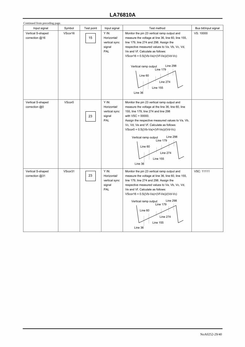
Vertical S-shaped correction @16
VScor16 Y IN: Horizontal/ vertical sync signal PAL
Monitor the pin 23 vertical ramp output and measure the voltage at line 36, line 60, line 155, line 179, line 274 and 298. Assign the respective measured values to Va, Vb, Vc, Vd, Ve and Vf. Calculate as follows: VScor16 = 0.5((Vb-Va)+(Vf-Ve))/(Vd-Vc)
VS: 10000
Vertical S-shaped correction @0
VScor0 Y IN: Horizontal/ vertical sync signal PAL
Monitor the pin 23 vertical ramp output and measure the voltage at the line 36, line 60, line 155, line 179, line 274 and line 298 with VSC = 00000. Assign the respective measured values to Va, Vb, Vc, Vd, Ve and Vf. Calculate as follows: VScor0 = 0.5((Vb-Va)+(Vf-Ve))/(Vd-Vc)
Vertical S-shaped correction @31
VScor31 Y IN: Horizontal/ vertical sync signal PAL
Monitor the pin 23 vertical ramp output and measure the voltage at line 36, line 60, line 155, line 179, line 274 and 298. Assign the respective measured values to Va, Vb, Vc, Vd, Ve and Vf. Calculate as follows: VScor16 = 0.5((Vb-Va)+(Vf-Ve))/(Vd-Vc)
VSC: 11111
15
23
23
Vertical ramp output
Line 155
Line 36
Line 274
Line 298
Line 60
Line 179
Vertical ramp output
Line 155
Line 36
Line 274
Line 298
Line 60
Line 179
Vertical ramp output
Line 155
Line 36
Line 274
Line 298
Line 60
Line 179
LA76810A
NoA0252-30/40
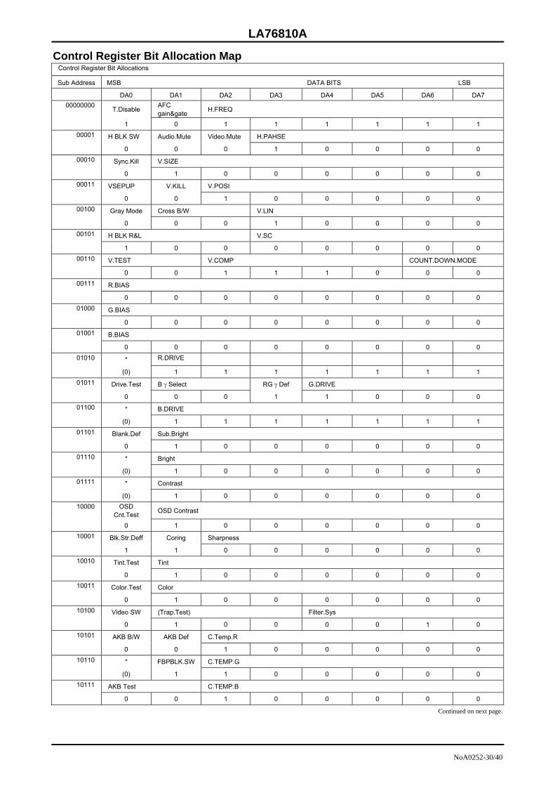
Control Register Bit Allocation Map Control Register Bit Allocations
Sub Address MSB DATA BITS LSB
DA0 DA1 DA2 DA3 DA4 DA5 DA6 DA7
T.Disable AFC gain&gate H.FREQ 00000000
1 0 1 1 1 1 1 1
H BLK SW Audio.Mute Video.Mute H.PAHSE 00001
0 0 0 1 0 0 0 0
Sync.Kill V.SIZE 00010
0 1 0 0 0 0 0 0
VSEPUP V.KILL V.POSI 00011
0 0 1 0 0 0 0 0
Gray Mode Cross B/W V.LIN 00100
0 0 0 1 0 0 0 0
H BLK R&L V.SC 00101
1 0 0 0 0 0 0 0
V.TEST V.COMP COUNT.DOWN.MODE 00110
0 0 1 1 1 0 0 0
R.BIAS 00111
0 0 0 0 0 0 0 0
G.BIAS 01000
0 0 0 0 0 0 0 0
B.BIAS 01001
0 0 0 0 0 0 0 0
* R.DRIVE 01010
(0) 1 1 1 1 1 1 1
Drive.Test B γ Select RG γ Def G.DRIVE 01011
0 0 0 1 1 0 0 0
* B.DRIVE 01100
(0) 1 1 1 1 1 1 1
Blank.Def Sub.Bright 01101
0 1 0 0 0 0 0 0
* Bright 01110
(0) 1 0 0 0 0 0 0
* Contrast 01111
(0) 1 0 0 0 0 0 0 OSD
Cnt.Test OSD Contrast 10000
0 1 0 0 0 0 0 0
Blk.Str.Deff Coring Sharpness 10001
1 1 0 0 0 0 0 0
Tint.Test Tint 10010
0 1 0 0 0 0 0 0
Color.Test Color 10011
0 1 0 0 0 0 0 0
Video SW (Trap.Test) Filter.Sys 10100
0 1 0 0 0 0 1 0
AKB B/W AKB Def C.Temp.R 10101
0 0 1 0 0 0 0 0
* FBPBLK.SW C.TEMP.G 10110
(0) 1 1 0 0 0 0 0
AKB Test C.TEMP.B 10111
0 0 1 0 0 0 0 0
Continued on next page.
LA76810A
NoA0252-31/40
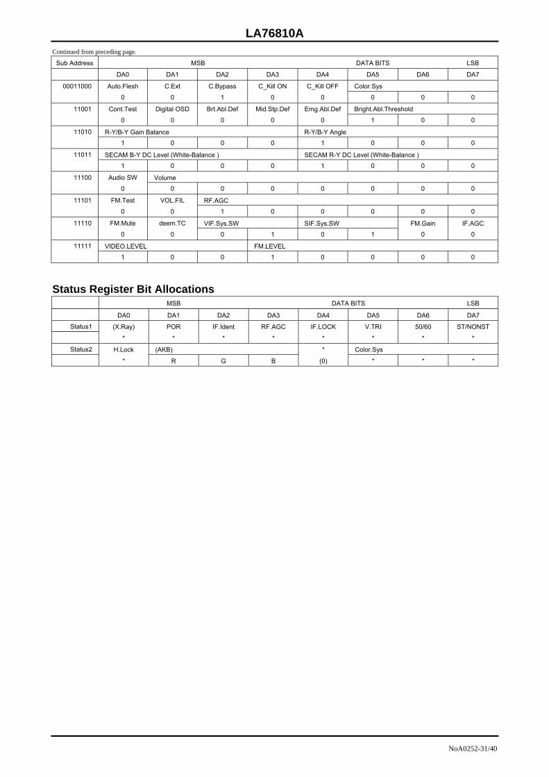
Continued from preceding page.
Sub Address MSB DATA BITS LSB
DA0 DA1 DA2 DA3 DA4 DA5 DA6 DA7
Auto.Flesh C.Ext C.Bypass C_Kill ON C_Kill OFF Color.Sys 00011000
0 0 1 0 0 0 0 0
Cont.Test Digital OSD Brt.Abl.Def Mid.Stp.Def Emg.Abl.Def Bright.Abl.Threshold 11001
0 0 0 0 0 1 0 0
R-Y/B-Y Gain Balance R-Y/B-Y Angle 11010
1 0 0 0 1 0 0 0
SECAM B-Y DC Level (White-Balance ) SECAM R-Y DC Level (White-Balance ) 11011
1 0 0 0 1 0 0 0
Audio SW Volume 11100
0 0 0 0 0 0 0 0
FM.Test VOL.FIL RF.AGC 11101
0 0 1 0 0 0 0 0
FM.Mute deem.TC VIF.Sys.SW SIF.Sys.SW FM.Gain IF.AGC 11110
0 0 0 1 0 1 0 0
VIDEO.LEVEL FM.LEVEL 11111
1 0 0 1 0 0 0 0
Status Register Bit Allocations
MSB DATA BITS LSB
DA0 DA1 DA2 DA3 DA4 DA5 DA6 DA7
Status1 (X.Ray) POR IF.Ident RF.AGC IF.LOCK V.TRI 50/60 ST/NONST
* * * * * * * *
Status2 H.Lock (AKB) * Color.Sys
* R G B (0) * * *
LA76810A
NoA0252-32/40
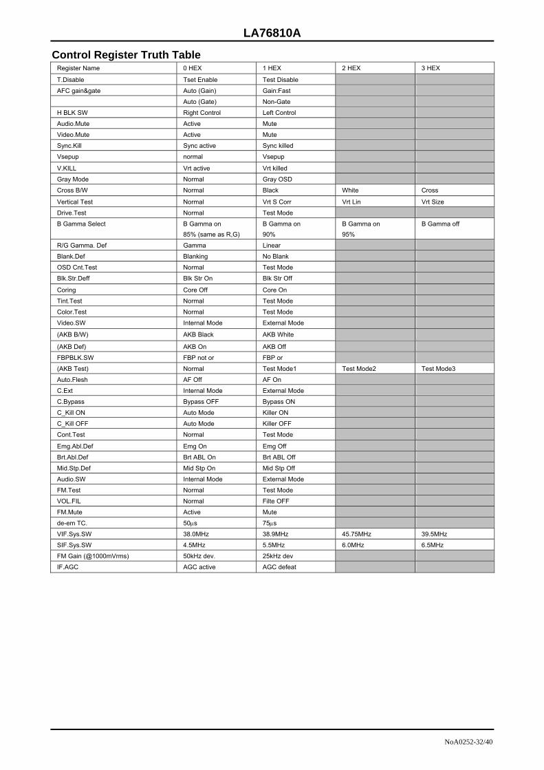
Control Register Truth Table Register Name 0 HEX 1 HEX 2 HEX 3 HEX
T.Disable Tset Enable Test Disable
AFC gain&gate Auto (Gain) Gain:Fast
Auto (Gate) Non-Gate
H BLK SW Right Control Left Control
Audio.Mute Active Mute
Video.Mute Active Mute
Sync.Kill Sync active Sync killed
Vsepup normal Vsepup
V.KILL Vrt active Vrt killed
Gray Mode Normal Gray OSD
Cross B/W Normal Black White Cross
Vertical Test Normal Vrt S Corr Vrt Lin Vrt Size
Drive.Test Normal Test Mode
B Gamma Select B Gamma on B Gamma on B Gamma on B Gamma off 85% (same as R,G) 90% 95%
R/G Gamma. Def Gamma Linear
Blank.Def Blanking No Blank
OSD Cnt.Test Normal Test Mode
Blk.Str.Deff Blk Str On Blk Str Off
Coring Core Off Core On
Tint.Test Normal Test Mode
Color.Test Normal Test Mode
Video.SW Internal Mode External Mode
(AKB B/W) AKB Black AKB White
(AKB Def) AKB On AKB Off
FBPBLK.SW FBP not or FBP or
(AKB Test) Normal Test Mode1 Test Mode2 Test Mode3
Auto.Flesh AF Off AF On
C.Ext Internal Mode External Mode
C.Bypass Bypass OFF Bypass ON
C_Kill ON Auto Mode Killer ON
C_Kill OFF Auto Mode Killer OFF
Cont.Test Normal Test Mode
Emg.Abl.Def Emg On Emg Off
Brt.Abl.Def Brt ABL On Brt ABL Off
Mid.Stp.Def Mid Stp On Mid Stp Off
Audio.SW Internal Mode External Mode
FM.Test Normal Test Mode
VOL.FIL Normal Filte OFF
FM.Mute Active Mute
de-em TC. 50µs 75µs
VIF.Sys.SW 38.0MHz 38.9MHz 45.75MHz 39.5MHz
SIF.Sys.SW 4.5MHz 5.5MHz 6.0MHz 6.5MHz
FM Gain (@1000mVrms) 50kHz dev. 25kHz dev
IF.AGC AGC active AGC defeat
LA76810A
NoA0252-33/40
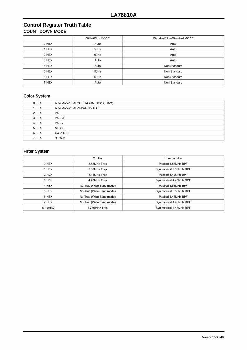
Control Register Truth Table COUNT DOWN MODE
50Hz/60Hz MODE Standard/Non-Standard MODE
0 HEX Auto Auto
1 HEX 50Hz Auto
2 HEX 60Hz Auto
3 HEX Auto Auto
4 HEX Auto Non-Standard
5 HEX 50Hz Non-Standard
6 HEX 60Hz Non-Standard
7 HEX Auto Non-Standard
Color System
0 HEX Auto Mode1 PAL/NTSC/4.43NTSC(/SECAM)
1 HEX Auto Mode2 PAL-M/PAL-N/NTSC
2 HEX PAL
3 HEX PAL-M
4 HEX PAL-N
5 HEX NTSC
6 HEX 4.43NTSC
7 HEX SECAM
Filter System
Y Filter Chroma Filter
0 HEX 3.58MHz Trap Peaked 3.58MHz BPF
1 HEX 3.58MHz Trap Symmetrical 3.58MHz BPF
2 HEX 4.43MHz Trap Peaked 4.43MHz BPF
3 HEX 4.43MHz Trap Symmetrical 4.43MHz BPF
4 HEX No Trap (Wide Band mode) Peaked 3.58MHz BPF
5 HEX No Trap (Wide Band mode) Symmetrical 3.58MHz BPF
6 HEX No Trap (Wide Band mode) Peaked 4.43MHz BPF
7 HEX No Trap (Wide Band mode) Symmetrical 4.43MHz BPF
8-15HEX 4.286MHz Trap Symmetrical 4.43MHz BPF
LA76810A
NoA0252-34/40
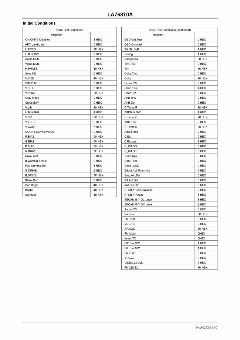
Initial Conditions Initial Test Conditions Initial Test Conditions (continued)
Register Register
ON/OFF(T.Disable) 1 HEX OSD Cnt.Test 0 HEX
AFC gain&gate 0 HEX OSD Contrast 0 HEX
H.FREQ 3F HEX Blk.Str.Deff 1 HEX
H BLK SW 0 HEX Coring 1 HEX
Audio.Mute 0 HEX Sharpness 00 HEX
Video.Mute 0 HEX Tint.Test 0 HEX
H.PHASE 10 HEX Tint 40 HEX
Sync.Kill 0 HEX Color.Test 0 HEX
V.SIZE 40 HEX Color 40 HEX
VSEPUP 0 HEX Video.SW 0 HEX
V.KILL 0 HEX (Trap.Test) 4 HEX
V.POSI 20 HEX Filter.Sys 0 HEX
Gray Mode 0 HEX AKB B/W 0 HEX
Cross B/W 0 HEX AKB Def 0 HEX
V.LIN 10 HEX C.Temp.R 20 HEX
H BLK R&L 4 HEX FBPBLK.SW 1 HEX
V.SC 00 HEX C.Temp.G 20 HEX
V.TEST 0 HEX AKB Test 0 HEX
V.COMP 7 HEX C.Temp.B 20 HEX
COUNT.DOWN.MODE 0 HEX Auto.Flesh 0 HEX
R.BIAS 00 HEX C.Ext 0 HEX
G.BIAS 00 HEX C.Bypass 1 HEX
B.BIAS 00 HEX C_Kill ON 0 HEX
R.DRIVE 7F HEX C_Kill OFF 0 HEX
Drive.Test 0 HEX Color Sys 0 HEX
B Gamma Select 0 HEX Cont.Test 0 HEX
R/G Gamma.Def 1 HEX Digitsl OSD 0 HEX
G.DRIVE 8 HEX Bright.Abl.Threshold 4 HEX
B.DRIVE 7F HEX Emg.Abl.Def 0 HEX
Blank.Def 0 HEX Brt.Abl.Def 0 HEX
Sub.Bright 40 HEX Mid.Stp.Def 0 HEX
Bright 40 HEX R-Y/B-Y Gain Balance 8 HEX
Contrast 40 HEX R-Y/B-Y Angle 8 HEX
SECAM B-Y DC Level 8 HEX
SECAM R-Y DC Level 8 HEX
Audio.SW 0 HEX
Volume 00 HEX
FM.Test 0 HEX
VOL.FIL 0 HEX
RF.AGC 20 HEX
FM.Mute 0HEX
deem.TC 0HEX
VIF.Sys.SW 1 HEX
SIF.Sys.SW 1 HEX
FM.Gain 0 HEX
IF.AGC 0 HEX
VIDEO.LEVEL 4 HEX
FM.LEVEL 10 HEX
LA76810A
NoA0252-35/40
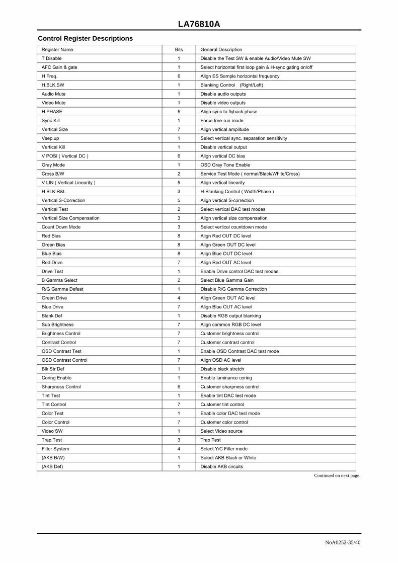
Control Register Descriptions Register Name Bits General Description
T Disable 1 Disable the Test SW & enable Audio/Video Mute SW
AFC Gain & gate 1 Select horizontal first loop gain & H-sync gating on/off
H Freq. 6 Align ES Sample horizontal frequency
H.BLK.SW 1 Blanking Control (Right/Left)
Audio Mute 1 Disable audio outputs
Video Mute 1 Disable video outputs
H PHASE 5 Align sync to flyback phase
Sync Kill 1 Force free-run mode
Vertical Size 7 Align vertical amplitude
Vsep.up 1 Select vertical sync. separation sensitivity
Vertical Kill 1 Disable vertical output
V POSI ( Vertical DC ) 6 Align vertical DC bias
Gray Mode 1 OSD Gray Tone Enable
Cross B/W 2 Service Test Mode ( normal/Black/White/Cross)
V LIN ( Vertical Linearity ) 5 Align vertical linearity
H BLK R&L 3 H-Blanking Control ( Width/Phase )
Vertical S-Correction 5 Align vertical S-correction
Vertical Test 2 Select vertical DAC test modes
Vertical Size Compensation 3 Align vertical size compensation
Count Down Mode 3 Select vertical countdown mode
Red Bias 8 Align Red OUT DC level
Green Bias 8 Align Green OUT DC level
Blue Bias 8 Align Blue OUT DC level
Red Drive 7 Align Red OUT AC level
Drive Test 1 Enable Drive control DAC test modes
B Gamma Select 2 Select Blue Gamma Gain
R/G Gamma Defeat 1 Disable R/G Gamma Correction
Green Drive 4 Align Green OUT AC level
Blue Drive 7 Align Blue OUT AC level
Blank Def 1 Disable RGB output blanking
Sub Brightness 7 Align common RGB DC level
Brightness Control 7 Customer brightness control
Contrast Control 7 Customer contrast control
OSD Contrast Test 1 Enable OSD Contrast DAC test mode
OSD Contrast Control 7 Align OSD AC level
Blk Str Def 1 Disable black stretch
Coring Enable 1 Enable luminance coring
Sharpness Control 6 Customer sharpness control
Tint Test 1 Enable tint DAC test mode
Tint Control 7 Customer tint control
Color Test 1 Enable color DAC test mode
Color Control 7 Customer color control
Video SW 1 Select Video source
Trap.Test 3 Trap Test
Filter System 4 Select Y/C Filter mode
(AKB B/W) 1 Select AKB Black or White
(AKB Def) 1 Disable AKB circuits
Continued on next page.
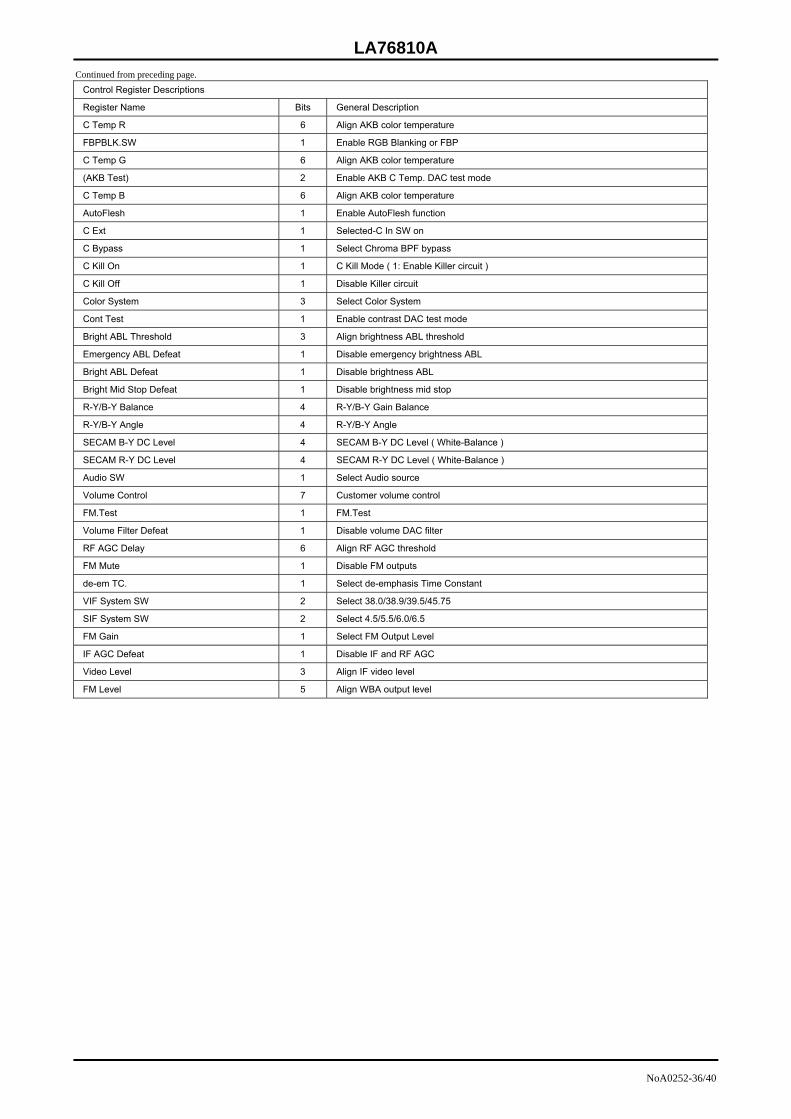
LA76810A
NoA0252-36/40
Continued from preceding page. Control Register Descriptions
Register Name Bits General Description
C Temp R 6 Align AKB color temperature
FBPBLK.SW 1 Enable RGB Blanking or FBP
C Temp G 6 Align AKB color temperature
(AKB Test) 2 Enable AKB C Temp. DAC test mode
C Temp B 6 Align AKB color temperature
AutoFlesh 1 Enable AutoFlesh function
C Ext 1 Selected-C In SW on
C Bypass 1 Select Chroma BPF bypass
C Kill On 1 C Kill Mode ( 1: Enable Killer circuit )
C Kill Off 1 Disable Killer circuit
Color System 3 Select Color System
Cont Test 1 Enable contrast DAC test mode
Bright ABL Threshold 3 Align brightness ABL threshold
Emergency ABL Defeat 1 Disable emergency brightness ABL
Bright ABL Defeat 1 Disable brightness ABL
Bright Mid Stop Defeat 1 Disable brightness mid stop
R-Y/B-Y Balance 4 R-Y/B-Y Gain Balance
R-Y/B-Y Angle 4 R-Y/B-Y Angle
SECAM B-Y DC Level 4 SECAM B-Y DC Level ( White-Balance )
SECAM R-Y DC Level 4 SECAM R-Y DC Level ( White-Balance )
Audio SW 1 Select Audio source
Volume Control 7 Customer volume control
FM.Test 1 FM.Test
Volume Filter Defeat 1 Disable volume DAC filter
RF AGC Delay 6 Align RF AGC threshold
FM Mute 1 Disable FM outputs
de-em TC. 1 Select de-emphasis Time Constant
VIF System SW 2 Select 38.0/38.9/39.5/45.75
SIF System SW 2 Select 4.5/5.5/6.0/6.5
FM Gain 1 Select FM Output Level
IF AGC Defeat 1 Disable IF and RF AGC
Video Level 3 Align IF video level
FM Level 5 Align WBA output level
LA76810A
NoA0252-37/40
Pin Assignment PIN FUNCTION PIN FUNCTION
1 Audio Output 54 SIF Input
2 FM Output 53 SIF APC Filter
3 PIF AGC 52 SIF Output
4 RF AGC Output 51 Ext. Audio Input
5 PIF Input1 50 APC Filter
6 PIF Input2 49 VCO Coil 1
7 IF Ground 48 VCO Coil 2
8 IF VCC 47 VCO Filter
9 FM Filter 46 Video Output
10 AFT Output 45 Black Level Detector
11 Bus Data 44 Internal Video Input (S-C IN)
12 Bus Clock 43 Video/Vertical VCC
13 ABL 42 External Video Input (Y IN)
14 Red Input 41 Video/Vertical/BUS Ground
15 Green Input 40 Selected Video Output
16 Blue Input 39 Chroma APC1 Filter
17 Fast Blanking Input 38 4.43MHz Crystal
18 RGB VCC 37 fsc (4.43MHz) Output
19 Red Output 36 ACC Filter
20 Green Output 35 SECAM R-Y Input
21 Blue Output 34 SECAM B-Y Input
22 Sync Sep Output 33 CCD/Horizontal Ground
23 Vertical Output 32 CCD Filter
24 Ramp ALC Filter 31 CCD VCC
25 Horizontal/BUS VCC 30 Clock (4MHz) Output
26 Horizontal AFC Filter 29 VCO IREF
27 Horizontal Output 28 Flyback Pulse Input
LA76810A
NoA0252-38/40
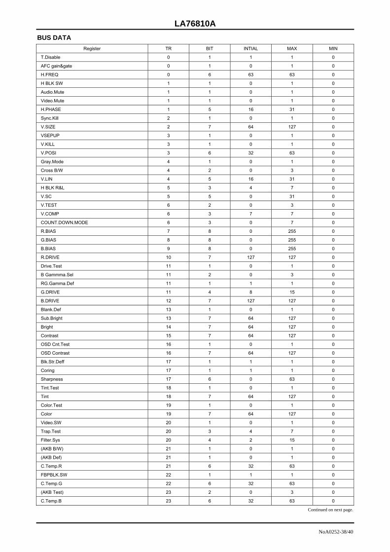
BUS DATA Register TR BIT INTIAL MAX MIN
T.Disable 0 1 1 1 0
AFC gain&gate 0 1 0 1 0
H.FREQ 0 6 63 63 0
H BLK SW 1 1 0 1 0
Audio.Mute 1 1 0 1 0
Video.Mute 1 1 0 1 0
H.PHASE 1 5 16 31 0
Sync.Kill 2 1 0 1 0
V.SIZE 2 7 64 127 0
VSEPUP 3 1 0 1 0
V.KILL 3 1 0 1 0
V.POSI 3 6 32 63 0
Gray.Mode 4 1 0 1 0
Cross B/W 4 2 0 3 0
V.LIN 4 5 16 31 0
H BLK R&L 5 3 4 7 0
V.SC 5 5 0 31 0
V.TEST 6 2 0 3 0
V.COMP 6 3 7 7 0
COUNT.DOWN.MODE 6 3 0 7 0
R.BIAS 7 8 0 255 0
G.BIAS 8 8 0 255 0
B.BIAS 9 8 0 255 0
R.DRIVE 10 7 127 127 0
Drive.Test 11 1 0 1 0
B Gammma.Sel 11 2 0 3 0
RG.Gamma.Def 11 1 1 1 0
G.DRIVE 11 4 8 15 0
B.DRIVE 12 7 127 127 0
Blank.Def 13 1 0 1 0
Sub.Bright 13 7 64 127 0
Bright 14 7 64 127 0
Contrast 15 7 64 127 0
OSD Cnt.Test 16 1 0 1 0
OSD Contrast 16 7 64 127 0
Blk.Str.Deff 17 1 1 1 0
Coring 17 1 1 1 0
Sharpness 17 6 0 63 0
Tint.Test 18 1 0 1 0
Tint 18 7 64 127 0
Color.Test 19 1 0 1 0
Color 19 7 64 127 0
Video.SW 20 1 0 1 0
Trap.Test 20 3 4 7 0
Filter.Sys 20 4 2 15 0
(AKB B/W) 21 1 0 1 0
(AKB Def) 21 1 0 1 0
C.Temp.R 21 6 32 63 0
FBPBLK.SW 22 1 1 1 0
C.Temp.G 22 6 32 63 0
(AKB Test) 23 2 0 3 0
C.Temp.B 23 6 32 63 0
Continued on next page.
LA76810A
NoA0252-39/40
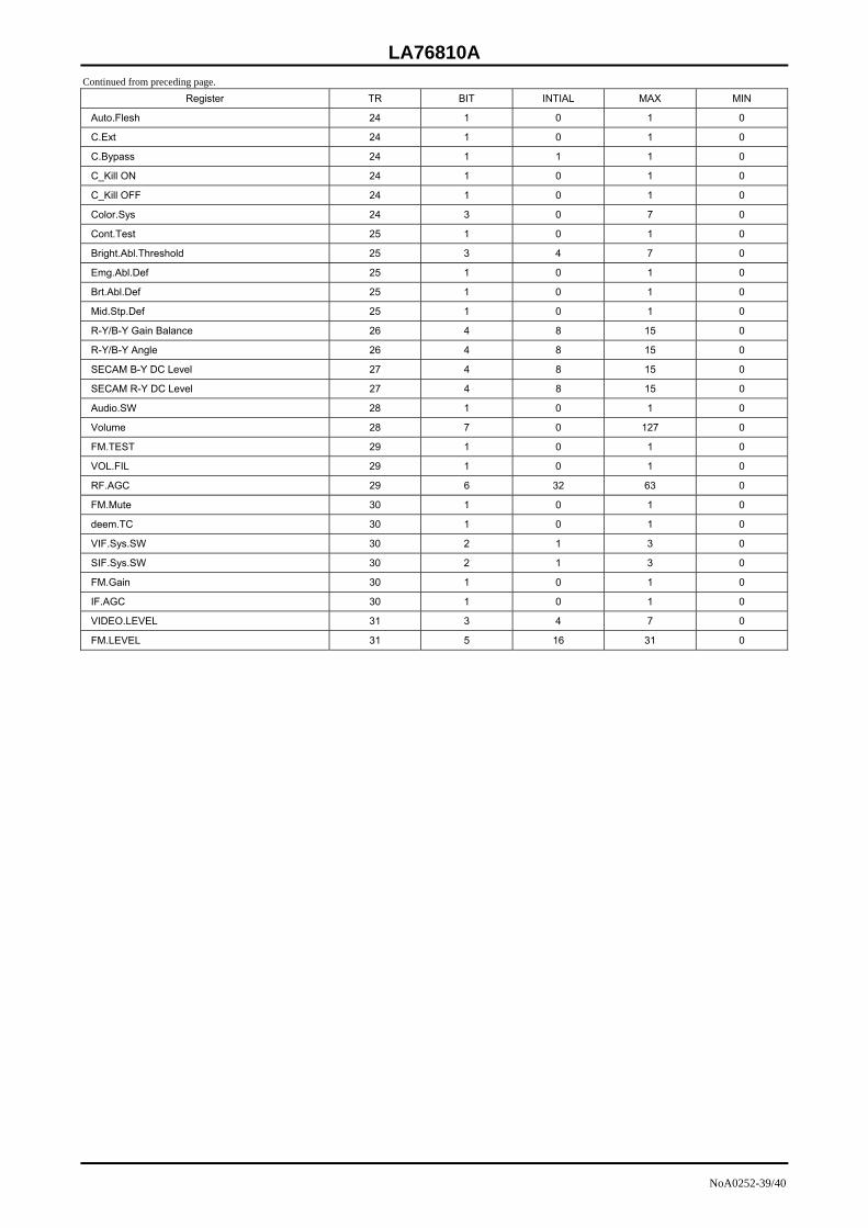
Continued from preceding page. Register TR BIT INTIAL MAX MIN
Auto.Flesh 24 1 0 1 0
C.Ext 24 1 0 1 0
C.Bypass 24 1 1 1 0
C_Kill ON 24 1 0 1 0
C_Kill OFF 24 1 0 1 0
Color.Sys 24 3 0 7 0
Cont.Test 25 1 0 1 0
Bright.Abl.Threshold 25 3 4 7 0
Emg.Abl.Def 25 1 0 1 0
Brt.Abl.Def 25 1 0 1 0
Mid.Stp.Def 25 1 0 1 0
R-Y/B-Y Gain Balance 26 4 8 15 0
R-Y/B-Y Angle 26 4 8 15 0
SECAM B-Y DC Level 27 4 8 15 0
SECAM R-Y DC Level 27 4 8 15 0
Audio.SW 28 1 0 1 0
Volume 28 7 0 127 0
FM.TEST 29 1 0 1 0
VOL.FIL 29 1 0 1 0
RF.AGC 29 6 32 63 0
FM.Mute 30 1 0 1 0
deem.TC 30 1 0 1 0
VIF.Sys.SW 30 2 1 3 0
SIF.Sys.SW 30 2 1 3 0
FM.Gain 30 1 0 1 0
IF.AGC 30 1 0 1 0
VIDEO.LEVEL 31 3 4 7 0
FM.LEVEL 31 5 16 31 0
LA76810A
PS NoA0252-40/40
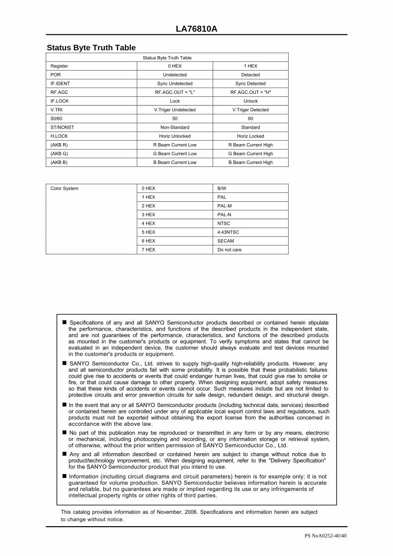
Status Byte Truth Table Status Byte Truth Table
Register 0 HEX 1 HEX
POR Undetected Detected
IF.IDENT Sync Undetected Sync Detected
RF.AGC RF.AGC.OUT = "L" RF.AGC.OUT = "H"
IF.LOCK Lock Unlock
V.TRI V.Triger Undetected V.Triger Detected
50/60 50 60
ST/NONST Non-Standard Standard
H.LOCK Horiz Unlocked Horiz Locked
(AKB R) R Beam Current Low R Beam Current High
(AKB G) G Beam Current Low G Beam Current High
(AKB B) B Beam Current Low B Beam Current High
0 HEX B/W
1 HEX PAL
2 HEX PAL-M
3 HEX PAL-N
4 HEX NTSC
5 HEX 4.43NTSC
6 HEX SECAM
Color System
7 HEX Do not care
Specifications of any and all SANYO Semiconductor products described or contained herein stipulate the performance, characteristics, and functions of the described products in the independent state, and are not guarantees of the performance, characteristics, and functions of the described products as mounted in the customer's products or equipment. To verify symptoms and states that cannot be evaluated in an independent device, the customer should always evaluate and test devices mounted in the customer's products or equipment.
SANYO Semiconductor Co., Ltd. strives to supply high-quality high-reliability products. However, any and all semiconductor products fail with some probability. It is possible that these probabilistic failures could give rise to accidents or events that could endanger human lives, that could give rise to smoke or fire, or that could cause damage to other property. When designing equipment, adopt safety measures so that these kinds of accidents or events cannot occur. Such measures include but are not limited to protective circuits and error prevention circuits for safe design, redundant design, and structural design.
In the event that any or all SANYO Semiconductor products (including technical data, services) described or contained herein are controlled under any of applicable local export control laws and regulations, such products must not be exported without obtaining the export license from the authorities concerned in accordance with the above law.
No part of this publication may be reproduced or transmitted in any form or by any means, electronic or mechanical, including photocopying and recording, or any information storage or retrieval system, of otherwise, without the prior written permission of SANYO Semiconductor Co., Ltd.
Any and all information described or contained herein are subject to change without notice due to product/technology improvement, etc. When designing equipment, refer to the "Delivery Specification" for the SANYO Semiconductor product that you intend to use.
Information (including circuit diagrams and circuit parameters) herein is for example only; it is not guaranteed for volume production. SANYO Semiconductor believes information herein is accurate and reliable, but no guarantees are made or implied regarding its use or any infringements of intellectual property rights or other rights of third parties.
This catalog provides information as of November, 2006. Specifications and information herein are subject to change without notice.