l-series power devices - abcelectronique
TRANSCRIPT

Powerex, Inc., 173 Pavilion Lane, Youngwood, Pennsylvania 15697 (724) 925-7272
L-Series Power Devices
Application Note

iii
Powerex, Inc., 173 Pavilion Lane, Youngwood, Pennsylvania 15697 (724) 925-7272
Application Information
1.0 Introduction ......................................................1
1.1 L-Series Intelligent Power Modules ....................1
1.2 L-Series High Power IPMs .................................1
1.3 L-Series Numbering System ..............................1
2.0 Definitions ........................................................2
3.0 Structure ...........................................................3
3.1 Ceramic Isolation Construction ..........................3
4.0 Installing IPMs ..................................................4
4.1 Application of Thermal Grease Example ............5
5.0 Thermal Impedance Considerations ..............6
6.0 IPM Self Protection ..........................................6
6.1 Self Protection Features .....................................6
6.2 Control Supply Under-voltage Lockout...............9
6.3 Over-temperature Protection ..............................9
6.4 Short-circuit Protection .....................................10
7.0 Controlling the Intelligent Power Module ....11
7.1 The Control Power Supply ...............................11
7.2 Interface Circuit Requirements .........................13
7.2.1 Other IPM Connection Requirements ....15
7.3 Speed Shifting Gate Drive................................16
7.4 Example Interface Circuits ...............................16
7.5 Connecting the Interface Circuit .......................17
7.6 Dead Time (tDEAD) ...........................................17
7.7 Using the fault signal ........................................17
7.8 IPM Inverter Examples .....................................21
8.0 Power Loss and Junction Temperature Calculations ....................................................22
9.0 Development Kits for L-Series IPMs ............23
Table of Contents


Powerex, Inc., 173 Pavilion Lane, Youngwood, Pennsylvania 15697 (724) 925-7272
1
PM 75 R L A 120
(1) (2) (3) (4) (5) (6)
(1) Device: PM = INTELLIMODTM (IPM)
(2) Current Rating: IC (Amperes)
(3) Power Transistors: C = 6-PAC R = 7-PAC (6-PAC + Brake)
(4) Device Series: L = L-Series
(5) Package:
A = Screw Power Terminals B = Pin Power Terminals
(6) Voltage: VCES Volts (x10)
1.0 Introduction to Intellimod™ Intelligent Power Modules
Powerex Intelligent Power Modules (IPMs) are advanced hybrid power devices that combine high speed, low loss IGBTs with optimized gate drive and protection circuitry. Highly effective short-circuit protection is realized through the use of ad-vanced current sense IGBT chips that allow continuous monitoring of power device current. System reliability is further enhanced by the IPM’s integrated over-temperature and under-voltage lock out protec-tion. Intelligent Power Modules are designed to reduce system size, cost, and time to market. Powerex in alliance with Mitsubishi Electric introduced the first full line of Intel-ligent Power Modules in November, 1991. Continuous improvements in power chip, packaging, and control circuit technology have lead to the L-Series IPM lineup shown in Table 1.1.
1.1 L-Series Intelligent Power Modules
The Powerex/Mitsubishi L-Series Intelligent Power Module family shown in Table 1.1 represents the industry’s most complete line of IPMs. The L-Series includes 37 types with ratings ranging from 25A to 450A for 1200V modules and 50A to 600A for 600V modules. The power semiconductors used in these 5th generation L-Series IPM modules are based on the field proven CSTBT IGBT and are the first IPMs to use the CSTBT technology. The L-Series has been optimized for minimum switching and conduction losses in order to meet industry demands for acousti-cally noiseless inverters with carrier
frequencies up to 20kHz. The built in gate drive and protection have been carefully designed to mini-mize the components required for the user supplied interface circuit.
1.2 L-Series High Power IPMs
The latest generation of IPM modules was developed in order to address newly emerging industry requirements for higher reliability, lower cost, and reduced EMI. By utilizing the low inductance packag-ing technology developed for the U-Series IGBT module combined with an advanced super soft free-wheel diode and optimized gate drive and protection circuits the L-Series IPM family achieves improved performance and compact size at reduced cost.
1.3 L-Series Numbering System
Table 1.1 L-Series Intelligent Power Modules
Part Number Current (A) Voltage (V) Brake Current (A)
PM50(#)L(*)060 50 600 30
PM75(#)L(*)060 75 600 50
PM100(#)LA060 100 600 50
PM150(#)LA060 150 600 75
PM200(#)LA060 200 600 100
PM300(#)LA060 300 600 150
PM450CLA060 450 600 NA
PM600CLA060 600 600 NA
PM25(#)L(*)120 25 1200 15
PM50(#)L(*)120 50 1200 25
PM75(#)L(*)120 75 1200 40
PM100(#)LA120 100 1200 50
PM150(#)LA120 150 1200 75
PM200CLA120 200 1200 NA
PM300CLA120 300 1200 NA
PM450CLA120 450 1200 NA
(*) Package Options: B = Solder Pin, A = Screw Terminal (#) Circuit Options: R = 7-PAC (6-PAC + Brake), C = 6-PACExample: PM75RLA060 is a 75A, 600V, 7-PAC (6-PAC + Brake) with Screw Terminals.

Powerex, Inc., 173 Pavilion Lane, Youngwood, Pennsylvania 15697 (724) 925-7272
2
2.0 Definitions
The tables in this section describe most of the terms that will be found in this application note and on the IPM datasheets. Table 2.1 gives definitions to the general symbols.
Table 2.2 gives the definitions to the symbols that are used on the Absolute Maximum Rating sec-tion of the device datasheets while
Table 2.1 General Definitions
Symbol Parameter Definition
IGBT Insulated Gate Bipolar Transistor
FWDi Free-wheeling Diode Anti-parallel to the IGBT
IPM Intelligent Power Module
tDEAD Dead Time Low side turn-off to high side turn-on and high side turn-off to low side turn-on
IPM Motor Interior Permanent Magnet Motor
(PC) Photo-coupler
PC Programmable Controller
CMR Common Mode Noise Rejection Maximum rise ratio to common mode voltage
CMH Maximum rise ratio of common mode voltage at the specific high level
CML Maximum rise ratio of common mode voltage at the specific low level
CTR Current Transfer Ratio Ratio of the output current to the Input current
Ta Ambient Temperature Atmosphere temperature without being subject to thermal source
TC Case Temperature Case temperature measured at specified point
Table 2.2 Absolute Maximum Ratings Definitions
Symbol Parameter Definition
VCES Collector-Emitter Blocking Voltage Maximum off-state collector-emitter voltage with gate-emitter shorted
IC Continuous Collector Current Maximum collector current – DC
ICM Peak Collector Current Repetitive Peak collector current, Tj ≤ 150°C
IE Continuous Diode Current Maximum diode current – DC
IEM Peak Diode Current Repetitive Diode peak current, Tj ≤ 150°C
PC Power Dissipation Maximum power dissipation (per device), TC = 25°C
Tj Junction Temperature Allowable range of IGBT junction temperature during operation
Tstg Storage Temperature Allowable range of temperature within which the module may be stored or transported without being subject to electric load
Viso Isolation Voltage Minimum RMS isolation voltage capability applied electric terminal to baseplate, 1 minute duration
— Mounting Torque Allowable tightening torque for terminal and mounting screws
Table 2.3 defines the symbols used in the Electrical Characteristics portion of the datasheets.

Powerex, Inc., 173 Pavilion Lane, Youngwood, Pennsylvania 15697 (724) 925-7272
3
3.0 Structure
Powerex Intelligent Power Modules utilize many of the same field prov-en module packaging technologies used in Powerex IGBT modules. Cost effective implementation of the built in gate drive and protec-tion circuits over a wide range of current ratings has been achieved. This packaging technology is described in more detail in section
3.1. L-Series IPMs are available in two power circuit configura-tions, 6-PAC (C), and 7-PAC (R). Figure 3.1 shows the L-Series power circuit configurations. Figure 3.2 shows the available L-Series package styles; the small pack-age in both screw terminal and pin terminal and the medium and large packages in screw terminal.
Table 2.3 Electrical Characteristics Definitions
Symbol Parameter Definition
ICES Collector-Emitter Leakage Current IC at VCE = VCES, VGE = 0V
VCE(sat) Collector-Emitter Saturation Voltage VCE at IC = rated IC and VGE = 15V
tC(on) Turn-on Delay Time Time from IC = 10% to VCE = 10% of final value
tC(off) Turn-off Delay Time Time from VCE = 10% of final value to IC = 10% of final value
Eon Turn-on Switching Loss Energy dissipated inside the IGBT during the turn-on of a single collector current pulse. Integral time starts from the 10% rise point of the collector current and ends at the 10% of the collector-emitter voltage point.
Eoff Turn-off Switching Loss Energy dissipated inside the IGBT during the turn-off of a single collector current pulse. Integral time starts from the 10% rise point of the collector-emitter voltage and ends at the specified low collector current point, 10% of IC.
trr Diode Reverse Recovery Time Time from IC = 0A to projection of zero IC from Irr and 0.5 x Irr points with IE = rated IC
VEC Forward Voltage Drop of Diode VEC at -IC = rated IC
Rth Thermal Resistance The rise of junction temperature per unit of power applied for a given time period
Rth(j-c) Thermal Resistance, Junction to Case IC conducting to establish thermal equilibrium
Rth(c-f) Thermal Resistance, Case to Fin IC conducting to establish thermal equilibrium lubricated
U
P
TYPE C
N
V W B
P
TYPE R
N
U V W
3.1 Ceramic Isolation Construction
The L-Series IPMs are constructed using ceramic isolation material. A direct bond copper process in which copper patterns are bonded directly to the ceramic substrate without the use of solder is used in these modules. This substrate provides the improved thermal characteristics and greater current carrying capabilities that are need-ed in these higher power devices. Gate drive and control circuits are contained on a separate PCB mounted directly above the power devices. The PCB is a multilayer construction with special shield lay-ers for EMI noise immunity. Figure 3.3 shows the cross-section of an L-Series Intelligent Power Module. The structure of the L-Series con-trol pin terminal is shown in Figure 3.4.Figure 3.1 L-Series Package Configurations

Powerex, Inc., 173 Pavilion Lane, Youngwood, Pennsylvania 15697 (724) 925-7272
4
MAIN ELECTRODE
INTERNALCONNECTIONTERMINAL
CONTROL PCB
WIRE
BASEPLATE CHIP INSULATED SUBSTRATE
GEL
CASE
RESIN
CONTROL INPUTTERMINAL
GUIDEPIN
Part Quality of Material UL Flame Class Main Electrode Copper Plated with Nickel Control Input Terminal Brass Plated with Gold Guide Pin PPS Resin UL 94-V0 Resin Epoxy UL 94-V0 Gel Silicone Case PPS Resin UL 94-V0 Wire Aluminum Chip Silicon Baseplate Copper Control PCB Glass Epoxy UL 94-V0 Insulated Substrate Ceramic Internal Connection Terminal Copper Plated with Nickel
Figure 3.2 L-Series Packages
L-SERIES SMALL PACkAGE WITH
PIN TERMINALS
L-SERIES SMALL PACkAGE WITH
SCREW TERMINALS
L-SERIES MEDIUM PACkAGE
4.0 Installing IPMs
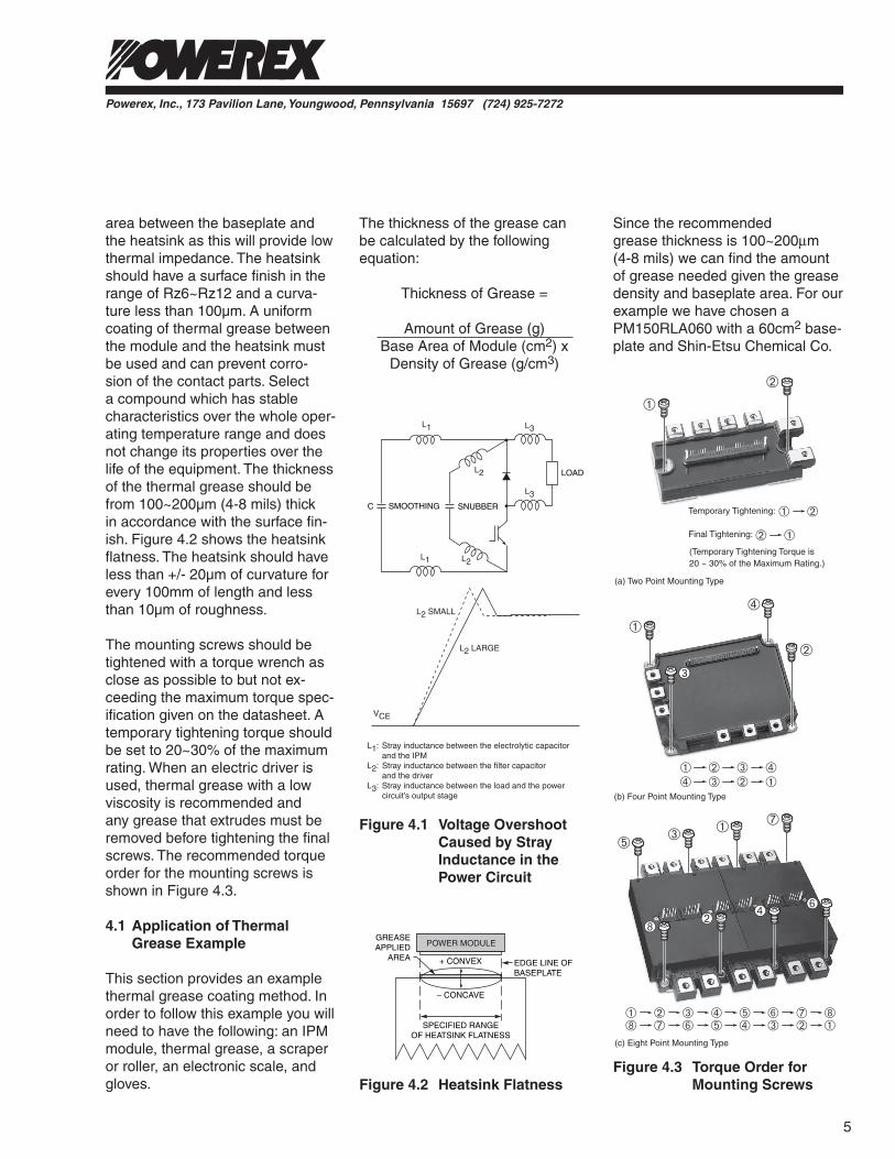
As Figure 4.1 shows, when the IPMs internal IGBTs are being switched off, voltage overshoot is introduced by the stray inductance of the power circuit as a result of the main current di/dt. The voltage overshoot can destroy the IPMs when the collector to emitter volt-age of the IGBTs goes above the device’s VCES rating. In order to avoid damaging an IPM due to an over-voltage the following recom-mendations should be implement-ed:
1. Locate the DC-link capacitor as close as possible to the IPM.
2. Use low impedance electrolytic capacitors for the DC-link.
3. Use low inductance parallel plates for the main conduction path from the DC-link capacitor to the IPM.
4. Use a film or ceramic capacitor mounted directly to the IPM’s P and N terminals to absorb surge voltage.
Uneven mounting stress should be avoided when attaching the modules to a heatsink because it can cause the ceramic isolation material in the modules to crack. It is best to have a large contact
L-SERIES LARGE PACkAGE
Figure 3.3 Cross-section of L-Series IPMs
Figure 3.4 Control Terminal of L-Series IPM
BRASS
NICKEL (Ni)THICKNESS = 1.5um
GOLD (Au)THICKNESS = 0.3um
Powerex, Inc., 173 Pavilion Lane, Youngwood, Pennsylvania 15697 (724) 925-7272
5
SMOOTHING SNUBBER
LOAD
C
L1
L3
L2
L1
L2
L3
L2 SMALL
L1: Stray inductance between the electrolytic capacitor and the IPML2: Stray inductance between the filter capacitor and the driverL3: Stray inductance between the load and the power circuit’s output stage
VCE
L2 LARGE
Figure 4.1 Voltage Overshoot Caused by Stray Inductance in the Power Circuit
area between the baseplate and the heatsink as this will provide low thermal impedance. The heatsink should have a surface finish in the range of Rz6~Rz12 and a curva-ture less than 100µm. A uniform coating of thermal grease between the module and the heatsink must be used and can prevent corro-sion of the contact parts. Select a compound which has stable characteristics over the whole oper-ating temperature range and does not change its properties over the life of the equipment. The thickness of the thermal grease should be from 100~200µm (4-8 mils) thick in accordance with the surface fin-ish. Figure 4.2 shows the heatsink flatness. The heatsink should have less than +/- 20µm of curvature for every 100mm of length and less than 10µm of roughness.
The mounting screws should be tightened with a torque wrench as close as possible to but not ex-ceeding the maximum torque spec-ification given on the datasheet. A temporary tightening torque should be set to 20~30% of the maximum rating. When an electric driver is used, thermal grease with a low viscosity is recommended and any grease that extrudes must be removed before tightening the final screws. The recommended torque order for the mounting screws is shown in Figure 4.3.
4.1 Application of Thermal Grease Example
This section provides an example thermal grease coating method. In order to follow this example you will need to have the following: an IPM module, thermal grease, a scraper or roller, an electronic scale, and gloves.
Since the recommended grease thickness is 100~200µm (4-8 mils) we can find the amount of grease needed given the grease density and baseplate area. For our example we have chosen a PM150RLA060 with a 60cm2 base-plate and Shin-Etsu Chemical Co.
+ CONVEX
– CONCAVE
EDGE LINE OFBASEPLATE
GREASEAPPLIED
AREA
SPECIFIED RANGEOF HEATSINK FLATNESS
POWER MODULE
Figure 4.2 Heatsink FlatnessFigure 4.3 Torque Order for
Mounting Screws
The thickness of the grease can be calculated by the following equation:
Thickness of Grease =
Amount of Grease (g) Base Area of Module (cm2) x
Density of Grease (g/cm3)
(a) Two Point Mounting Type
(c) Eight Point Mounting Type
� �� �
��
��
��
��
��
��
�
�
�� � �
�
�
�
�
�� � �
(b) Four Point Mounting Type
� �� �
��
��
Temporary Tightening:
Final Tightening:
(Temporary Tightening Torque is 20 ~ 30% of the Maximum Rating.)
� �
� �
Powerex, Inc., 173 Pavilion Lane, Youngwood, Pennsylvania 15697 (724) 925-7272
6
G-746 grease having a density of 2.66g/cm3.
100~200µm =
Amount of Grease (g) 60cm2 x 2.66g/cm3
∴The amount needed is 1.6~3.2g
Once the amount of required grease has been calculated the grease can be applied uniformly across the baseplate using a scraper or a roller and a mask.
See Table 4.1 for a list of recom-mended thermal compounds.
5.0 Thermal Impedance Considerations
The junction to case thermal resis-tance (Rth(j-c)) and the case to heat sink thermal resistance (Rth(c-f)) are given on the individual device datasheets. Table 5.1 shows the thermal resistance values for the L-Series IPMs. The case temperature is measured just below the chip and the chip
Table 4.1 Thermal Compounds
Manufacturer Type
Shin-Etsu Chemical Co., Ltd. GE Toshiba Silicones
kS-609, G-747, G-746 YG6260
DOW CORNING DC 340
For more information, please refer to manufacturers.
locations as shown in Tables 5.2, 5.3 and 5.4. The thermal resis-tance is measured using a uniform 100~200µm coating of thermal grease, with a thermal conductivity of 0.92W/m*°C, between the module and the heatsink. A thermocouple is used to measure the case and heatsink temperature along the same vertical line as shown in Figure 5.1.
Table 5.1 Thermal Resistance Values for L-Series IPMs
Type Name
Inverter(Just Under the Chip)
Brake(Just Under the Chip)
ContactThermal Resistance
Rth(c-f)IGBT Chip Rth(j-c)Q FWDi Chip Rth(j-c) IGBT Chip Rth(j-c)Q FWDi Chip Rth(j-c)
600V Type
PM50RLA/B060, PM50CLA/B060 0.95 1.61 1.21 2.19 0.038
PM75RLA/B060, PM75CLA/B060 0.32 0.53 0.42 0.71 0.038
PM100RLA/B060, PM100CLA/B060 0.27 0.43 0.42 0.71 0.038
PM150RLA/B060, PM150CLA/B060 0.20 0.33 0.32 0.53 0.038
PM200RLA/CLA060 0.16 0.25 0.28 0.44 0.023
PM300RLA/CLA060 0.12 0.19 0.21 0.34 0.023
PM450CLA060 0.12 0.19 — — 0.014
PM600CLA060 0.07 0.11 — — 0.014
1200V Type
PM25RLA/B120, PM25CLA/B120 0.83 1.36 0.96 1.82 0.038
PM50RLA/B120, PM50CLA/B120 0.26 0.39 0.36 0.60 0.038
PM75RLA/B120, PM75CLA/B120 0.21 0.30 0.28 0.45 0.038
PM100RLA/B120, PM100CLA/B120 0.16 0.26 0.26 0.40 0.023
PM150RLA/B120, PM150CLA/B120 0.12 0.20 0.21 0.31 0.023
PM200CLA120 0.12 0.20 — — 0.014
PM300CLA120 0.08 0.13 — — 0.014
PM450CLA120 0.05 0.09 — — 0.014

Powerex, Inc., 173 Pavilion Lane, Youngwood, Pennsylvania 15697 (724) 925-7272
7
Table 5.2 Chip Layout (Small Package)
Type NameUP VP WP UN VN WN Br
IGBT FWDi IGBT FWDi IGBT FWDi IGBT FWDi IGBT FWDi IGBT FWDi IGBT FWDi
600V Type
PM50RLA/RLB060, PM50CLA/CLB060
X 29.0 29.5 64.6 65.1 85.9 86.4 38.1 37.6 54.8 55.3 76.1 75.6 18.3 22.4
Y -7.3 1.6 -7.3 2.1 -7.3 2.1 5.3 -4.6 5.3 -4.6 5.3 -4.6 -7.4 7.0
PM75RLA/RLB060, PM75CLA/CLB060
X 28.7 28.7 65.2 65.2 85.3 85.3 38.0 38.0 55.4 55.4 75.5 75.5 19.0 23.0
Y -6.6 0.8 -6.6 2.5 -6.6 2.5 4.6 -4.5 4.6 -4.5 4.6 -4.5 -7.3 6.6
PM100RLA060, PM100CLA060
X 28.3 28.0 65.0 65.2 87.0 87.2 39.3 39.5 54.0 53.7 76.0 75.7 17.5 18.7
Y -8.5 1.7 -8.5 1.7 8.5 1.7 6.5 -5.2 6.5 -5.2 6.5 -5.2 -10.4 4.0
PM150RLA060, PM150CLA060
X 28.3 28.3 65.0 65.0 87.0 87.0 39.3 39.3 54.0 54.0 76.0 76.0 18.1 18.1
Y -7.7 2.4 -7.7 2.4 -7.7 2.4 5.7 -4.4 5.7 -4.4 5.7 -4.4 -10.5 4.0
1200V Type
PM25RLA/RLB120, PM25CLA/CLB120
X 29.0 29.3 65.0 65.5 85.6 85.9 37.8 37.5 55.2 55.7 75.8 75.3 19.0 22.3
Y -7.1 1.5 -7.1 2.0 -7.1 2.0 5.1 -4.5 5.1 -4.5 5.1 -4.5 -7.3 6.6
PM50RLA/RLB120, PM50CLA/CLB120
X 28.3 28.4 65.0 64.9 87.0 86.9 39.3 39.2 54.0 54.1 76.0 76.1 17.9 19.3
Y -7.7 1.5 -7.7 1.5 -7.7 1.5 5.7 -3.5 5.7 -3.5 5.7 -3.5 -10.5 4.3
PM75RLA/RLB120, PM75CLA/CLB120
X 28.3 28.3 65.0 65.0 87.0 87.0 39.3 39.3 54.0 54.0 76.0 76.0 18.1 18.0
Y -8.2 2.0 -8.2 2.0 -8.2 2.0 6.2 -4.0 6.2 -4.0 6.2 -4.0 -10.1 5.6
Y SMALL PACKAGEBACK SIDE
X
DC supply. Specially designed gate drive circuits eliminate the need for a negative supply to off bias the IGBT. The IPM’s control input is designed to interface with opto-coupled transistors with a minimum of external components. The opera-tion and timing of each protection feature is described in Sections 6.2 through 6.4.
Control supply under-voltage, over-temperature, over-current, and short-circuit protection are all provided by the IPM’s internal gate control circuits. A fault output signal is provided to alert the system controller if any of the protection circuits are activated. Figure 6.1 is a block diagram showing the IPM’s internally integrated functions. This diagram also shows the isolated interface circuits and control power supply that must be provided by the user. The internal gate control circuit requires only a simple +15V
6.0 IPM Self Protection
6.1 Self Protection Features
Intelligent Power Modules have sophisticated built-in protection circuits that prevent the power devices from being damaged should the system malfunction or be over stressed. Our design and applications engineers have developed fault detection and shut down schemes that allow maximum utilization of power device capabil-ity without compromising reliability.

Powerex, Inc., 173 Pavilion Lane, Youngwood, Pennsylvania 15697 (724) 925-7272
8
Table 5.3 Chip Layout (Medium Package)
Type NameUP VP WP UN VN WN Br
IGBT FWDi IGBT FWDi IGBT FWDi IGBT FWDi IGBT FWDi IGBT FWDi IGBT FWDi
600V Type
PM200RLA060, PM200CLA060
X 23.7 23.0 57.2 56.5 87.7 86.5 37.7 38.0 70.2 71.5 100.7 101.5 11.0 7.7
Y 56.7 43.7 56.7 43.7 56.7 43.7 28.7 41.8 28.7 41.8 28.7 41.8 26.7 60.9
PM300RLA060, PM300CLA060
X 23.0 23.0 57.5 56.5 87.5 86.5 37.0 38.0 70.5 71.5 100.5 101.5 11.0 8.0
Y 56.3 42.7 56.3 42.7 56.3 42.7 29.1 42.7 29.1 42.7 29.1 42.7 27.1 60.7
1200V Type
PM100RLA120, PM100CLA120
X 23.7 23.0 57.2 56.5 87.7 86.5 37.7 38.0 70.2 71.5 100.7 101.5 10.8 7.2
Y 56.7 43.4 56.7 43.4 56.7 43.4 28.7 42.0 28.7 42.0 28.7 42.0 26.9 60.6
PM150RLA120, PM150CLA120
X 23.0 23.0 57.5 56.5 87.5 86.5 37.0 38.0 70.5 71.5 100.5 101.5 11.0 8.0
Y 56.3 43.1 56.3 43.1 56.3 43.1 29.1 42.4 29.1 42.4 29.1 42.4 26.8 61.0
Table 5.4 Chip Layout (Large Package)
Type NameUP VP WP UN VN WN
IGBT FWDi IGBT FWDi IGBT FWDi IGBT FWDi IGBT FWDi IGBT FWDi
600V Type
PM450CLA060X 26.5 23.9 76.5 73.9 126.5 123.9 23.4 26.0 73.4 76.0 123.4 126.0
Y 85.5 70.5 85.5 70.5 85.5 70.5 24.5 39.5 24.5 39.5 24.5 39.5
PM600CLA060X 30.5 20.4 80.5 70.4 130.5 120.4 19.4 29.6 69.4 79.6 119.4 129.6
Y 82.8 82.8 82.8 82.8 82.8 82.8 27.2 27.2 27.2 27.2 27.2 27.2
1200V Type
PM200CLA120X 26.5 23.6 76.5 73.6 126.5 123.6 23.4 26.4 73.4 76.4 123.4 126.4
Y 85.5 70.5 85.5 70.5 85.5 70.5 24.5 39.5 24.5 39.5 24.5 39.5
PM300CLA120X 30.1 19.2 80.1 69.2 130.1 119.2 19.8 30.7 69.8 80.7 119.8 130.7
Y 89.4 89.4 89.4 89.4 89.4 89.4 20.6 20.6 20.6 20.6 20.6 20.6
PM450CLA120X 30.1 19.2 80.1 69.2 130.1 119.2 19.8 30.7 69.8 80.7 119.8 130.7
Y 82.7 82.7 82.7 82.7 82.7 82.7 27.2 27.2 27.2 27.2 27.2 27.2
MEDIUM PACKAGEBACK SIDE
Y
X
LARGE PACKAGEBACK SIDE
Y
X

Powerex, Inc., 173 Pavilion Lane, Youngwood, Pennsylvania 15697 (724) 925-7272
9
6.2 Control Supply Under-voltage Lock Out
The Intelligent Power Module’s internal control circuits operate from an isolated 15V DC supply. If, for any reason, the voltage of this supply drops below the specified under-voltage trip level (UVt), the power devices will be turned off and a fault signal will be generated. Small glitches less than the speci-fied tdUV in length will not affect the operation of the control circuitry
and will be ignored by the under-voltage protection circuit. In order for normal operation to resume, the supply voltage must exceed the under-voltage reset level (UVr) for a time greater than the fault output delay (tfo). Operation of the under-voltage protection circuit will also occur during power up and power down of the control supply. This operation is normal and the system controller’s program should take the fault output delay (tfo) into account. Figure 6.2 is a timing dia-
gram showing the operation of the under-voltage lock-out protection circuit. In this diagram an active low input signal is applied to the input pin of the IPM by the system con-troller. The effects of control supply power up, power down and failure on the power device gate drive and fault output are shown.
Caution:
1. Application of the main bus voltage at a rate greater than 20V/µs before the control power supply is on and stabilized may cause destruction of the power devices.
2. Voltage ripple on the control power supply with dv/dt in excess of 5V/µs may cause a false trip of the UV lock-out.
6.3 Over-temperature Protection
The L-Series Intelligent Power Module has a temperature detector on each chip. If the temperature at any chip junction on the L-Series module exceeds the over- temperature trip level (OT) the IPM’s internal control circuit will protect the power devices by dis-abling the gate drive and ignoring the control input signal until the over-temperature condition has subsided. In 6-PAC and 7-PAC modules all three low side devices will be turned off and a low side fault signal will be generated. High side switches are unaffected and can still be turned on and off by the system controller. The fault output will remain as long as the over-tem-perature condition exists. When the temperature falls below the over-temperature reset level (OTr), and the control input is high (off-state) the power device will be enabled and normal operation will resume at the next low (on) input signal.
MODULE
FIN
METALLICBASEPLATE
IGBTCHIP
NOTE:
TC TSINK
Figure 5.1 Thermal Measurement Points
GATECONTROLCIRCUIT
ISOLATINGINTERFACE
CIRCUIT
ISOLATINGINTERFACE
CIRCUIT
ISOLATEDPOWERSUPPLY
INTELLIGENT POWER MODULE
SENSECURRENT
INPUTSIGNAL
FAULTOUTPUT
CURRENTSENSEIGBT
COLLECTOR
EMITTER
TEMPERATURESENSOR
GATE DRIVEOVER-TEMPUV LOCK-OUTOVER-CURRENTSHORT-CIRCUIT
Figure 6.1 IPM Gate Drive Circuit

Powerex, Inc., 173 Pavilion Lane, Youngwood, Pennsylvania 15697 (724) 925-7272
10
Figure 6.3 is a timing diagram showing the operation of the over-temperature protection circuit. The over-temperature function provides effective protection against over-loads and cooling system failures in most applications. In cases of abnormally high losses such as failure of the system controller to properly regulate current or exces-sively high switching frequency, it is possible for the center of the IGBT chip to exceed Tj(max) before the on-chip temperature sensor reaches the OT trip level.
Caution: Tripping of the over- temperature protection is an indication of stressful operation. Repetitive tripping should be avoided.
6.4 Short-circuit Protection
The IPM uses current sense IGBT chips to continuously monitor power device current. If the current though the Intelligent Power Module exceeds the specified short-circuit trip level (SC) for a period longer than toff(SC), the IPMs internal control circuit will pro-tect the power device by disabling the gate drive and generating a fault output signal. The timing of the short-circuit protection is shown in Figure 6.4. The toff(SC) delay is implemented in order to avoid trip-ping of the SC protection on short pulses of current above the SC level that are not dangerous for the power device. When a short-circuit is detected a controlled shutdown is initiated and a fault output is generated. The controlled shut-down lowers the turn-off di/dt which helps to control transient voltages that can occur during shut down from high fault currents. Most Intel-ligent Modules use the two step shutdown depicted in Figure 6.4.
In the two step shutdown, the gate voltage is reduced to an interme-diate voltage causing the current through the device to drop slowly to a low level. Then, about 5µs later, the gate voltage is reduced to zero completing the shut down. The Intellimod™ uses actual device
current measurements to detect all short-circuit current conditions. Even resistive and inductive shorts to ground that are often missed by conventional desaturation and bus current sensing protection schemes will be detected by the Intellimod™’s current sense IGBTs.
tFO
CONTROL SUPPLY ON CONTROL SUPPLY OFFSHORTGLITCH
IGNORED
POWER SUPPLYFAULT ANDRECOVERY
tFOtdUV
UVr
INPUTSIGNAL
CONTROLSUPPLY
VOLTAGE
FAULTOUTPUT
CURRENT(IFO)
INTERNALGATE
VOLTAGE(VGE)
UVt
tdUV
OT
INPUTSIGNAL
CHIPTEMPERATURE
(TC)
FAULTOUTPUT
CURRENT(IFO)
INTERNALGATE
VOLTAGE(VGE)
OTr
Figure 6.3 Operation of Over-temperature
Figure 6.2 Operation of Under-voltage Lockout

Powerex, Inc., 173 Pavilion Lane, Youngwood, Pennsylvania 15697 (724) 925-7272
11
Caution:
1. Tripping of the short-circuit protection indicates stressful operation of the IGBT. Repetitive tripping must be avoided.
2. High surge voltages can occur during emergency shutdown.
Low inductance buswork and snub-bers are recommended.
7.0 Controlling the Intelligent Power Module
Intelligent Power Modules are easy to operate. The integrated gate drive and protection circuits require only an isolated power supply and an active low control signal. A fault output is provided for monitoring the operation of the modules inter-nal protection circuits.
7.1 The Control Power Supply
Depending on the power circuit configuration of the module two, four or six isolated power supplies are required by the IPM’s internal drive and protection circuits. In high power 3-phase inverters using the larger 6-PAC type IPMs six isolated power supplies must be used. In these high current applications each low side device must have its own isolated control power supply in order to avoid ground loop noise problems. The control supplies should be regulated to 15V +/-10% in order to avoid over-voltage dam-age or false tripping of the under-voltage protection. The supplies should have an isolation voltage rating of at least two times the IPM’s VCES rating (i.e. Viso = 2400V for 1200V module). The current that
must be supplied by the control power supply is the sum of the quiescent current needed to power the internal control circuits and the current required to drive the IGBT gate.
Table 7.1 summarizes control supply requirements for L-Series IPMs. This table gives control circuit currents for the quiescent (non-switching) state and for 20kHz switching. This data is provided in order to help the user design appropriately sized control power supplies.
Power requirements for operat-ing frequencies other than 20kHz can be determined by scaling the frequency dependent portion of the control circuit current. For example, to determine the maximum con-trol circuit current required for the low side (N) of a PM75RLA120 operating at 7kHz the maximum quiescent control circuit current is subtracted from the maximum 20kHz control circuit current:
42mA – 19mA = 23mA
23mA is the frequency dependent portion of the control circuit cur-rent for 20kHz operation. For 7kHz operation the frequency dependent portion is:
23mA x (7kHz / 20kHz) = 8.05mA
To get the total control power sup-ply current required, the quiescent current must be added back:
19mA + 8.05mA = 27.05mA
27.05mA is the maximum control circuit current required for the low side (N) of a PM75RLA120 operat-ing at 7kHz.
NORMAL OPERATIONFWD RECOVERY CURRENT
NORMAL OPERATIONOVER-CURRENTFAULT ANDRECOVERY
tFO
INPUTSIGNAL
INTERNALGATE
VOLTAGE(VGE)
FAULT OUTPUT
CURRENT(IFO)
COLLECTORCURRENT
SHORT-CIRCUITTRIP LEVEL
toff(SC)
thold
Figure 6.4 Operation of Short-circuit Protection
Powerex, Inc., 173 Pavilion Lane, Youngwood, Pennsylvania 15697 (724) 925-7272
12
We can use the same technique described here to determine the control supply current required by each of the high side (P) IGBTs of the IPM.
Capacitive coupling between primary and secondary sides of isolated control supplies must be minimized as parasitic capacitanc-es in excess of 100pF can cause noise that may trigger the control circuits. An electrolytic or tantalum decoupling capacitor should be connected across the control power supply at the IPM’s terminals. This capacitor will help to filter common noise on the control power supply and provide the high pulse currents required by the IPM’s internal gate drive circuits. Isolated control pow-er supplies can be created using a variety of techniques. Control pow-er can be derived from the main input line using either a switching power supply with multiple outputs or a line frequency transformer with multiple secondaries. Control power supplies can also be derived from the main logic power supply using DC-to-DC converters. Using a compact DC-to-DC converter for each isolated supply can help to simplify the interface circuit layout. A distributed DC-to-DC converter in which a single oscillator is used to drive several small isolation transformers can provide the layout advantages of separate DC-to-DC converters at a lower cost.
In order to simplify the design of the required isolated power supplies, Powerex has developed DC-to-DC converter modules to work with the IPMs. 20V DC can be connected to the M57140-01 to produce four isolated 15V DC outputs to power the IPM’s control circuits. The M57140-01 can also be used as a stand alone unit if
Table 7.1 L-Series IPM Control Power Supply Current
Part NumberN Side (Each Supply) P Side (Each Supply)
DC 20kHz DC 20kHz
600V Series
PM50CLA060 11.0 21.0 3.5 7.0
PM50CLB060 11.0 21.0 3.5 7.0
PM50RLA060 10.5 25.0 4.0 7.5
PM50RLB060 10.5 25.0 4.0 7.5
PM75CLA060 13.0 27.5 4.5 9.0
PM75CLB060 13.0 27.5 4.5 9.0
PM75RLA060 17.5 33.0 5.0 10.0
PM75RLB060 17.5 33.0 5.0 10.0
PM100CLA060 15.0 32.0 4.0 11.0
PM100RLA060 19.0 38.0 5.0 11.0
PM150CLA060 15.0 33.0 5.0 14.0
PM150RLA060 24.0 52.0 6.0 15.0
PM200CLA060 18.0 58.0 6.0 15.0
PM200RLA060 22.5 59.0 6.0 18.0
PM300CLA060 20.5 79.0 6.0 25.0
PM300RLA060 25.0 82.5 6.5 25.0
PM450CLA060 11.0 31.0 11.0 31.0
PM600CLA060 20.0 53.0 20.0 53.0
1200V Series
PM25CLA120 12.0 19.0 4.0 7.0
PM25CLB120 12.0 19.0 4.0 7.0
PM25RLA120 16.0 24.0 4.0 6.5
PM25RLB120 16.0 24.0 4.0 6.5
PM50CLA120 17.0 30.0 5.0 10.0
PM50CLB120 17.0 30.0 5.0 10.0
PM50RLA120 19.0 33.0 5.0 10.0
PM50RLB120 19.0 33.0 5.0 10.0
PM75CLA120 17.0 30.0 5.0 10.0
PM75CLB120 17.0 30.0 5.0 10.0
PM75RLA120 19.0 42.0 5.0 12.5
PM75RLB120 19.0 42.0 5.0 12.5
PM100CLA120 16.0 50.0 5.0 17.0
PM100RLA120 20.0 53.0 5.0 16.0
PM150CLA120 20.0 67.5 6.0 21.0
PM150RLA120 24.0 76.0 6.0 23.0
PM200CLA120 20.0 39.0 20.0 39.0
PM450CLA120 20.0 98.0 30.0 98.0

Powerex, Inc., 173 Pavilion Lane, Youngwood, Pennsylvania 15697 (724) 925-7272
13
20V DC is available from another source such as the main logic power supply.
24V DC can be connected to the VLA106-24151 and VLA106-24154 to produce a single isolated 15V DC to power the IPM control circuits. The VLA106-24151 has an output capability of 100mA, while the VLA106-24154 has an output capability of 300mA which may be needed with the larger size IPMs. Figure 7.2 shows an isolated interface circuit for a seven pack IPM using Powerex DC-to-DC converters. Section 9 gives details of Powerex development kits that employ this interface circuit.
Caution: Using bootstrap techniques is not recommended because the voltage ripple on VD may cause a false trip of the under-voltage protection in certain inverter PWM modes.
7.2 Interface Circuit Requirements
The IGBT power switches in the Powerex IPM modules are con-trolled by a low level input signal. The active low control input will keep the power devices off when it is held high. Typically the input pin of the IPM is pulled high with a resistor connected to the positive side of the control power supply. An ON signal is then generated by pulling the control input low. The fault output is an open collector with its maximum sink current inter-nally limited. When a fault condition occurs the open collector device turns on allowing the fault output to sink current from the positive side of the control supply. Fault and on/off control signals are usually transferred to and from the system controller using isolating interface
circuits. Isolating interfaces allow high and low side control signals to be referenced to a common logic level. The isolation is usually pro-vided by opto-couplers. However, fiber optics, pulse transformers, or level shifting circuits could be used. The most important consideration in interface circuit design is layout. Shielding and careful routing of printed circuit wiring is necessary in order to avoid coupling of dV/dt noise into control circuits. Parasitic capacitance between high side interface circuits, high and low side interface circuits or primary and secondary sides of the iso-lating devices can cause noise problems. Careful layout of con- trol power supply and isolating circuit wiring is necessary. The L-Series design kits are discussed in more detail in Section 9.0.
Figure 7.1 shows the interface circuit layout used in the L- Series BP7A design kit and Figure 7.2 shows the board layout. The shielding and printed circuit routing techniques used in this example are intended to illustrate a typical application of the layout guidelines. The following is a list of guidelines that should be followed when designing interface circuits.
INTERFACE CIRCUIT LAYOUT GUIDELINES
1. Maintain maximum interface isolation. Avoid routing printed circuit board traces from primary and secondary sides of the iso-lation device near to or above and below each other. Any lay-out that increases the primary to secondary capacitance of the isolating interface can cause noise problems.
2. Maintain maximum control power supply isolation. Avoid
routing printed circuit board traces from UP, VP, WP, and N side supplies near to each other. High dV/dts exist between these supplies and noise will be coupled through parasitic capacitances. If isolated power supplies are derived from a common transformer inter- winding capacitance should be minimized.
3. keep printed circuit board traces between the interface circuit and Intellimod™ short. Long traces have a tendency to pick up noise from other parts of the circuit.
4. Use recommended decoupling capacitors for power supplies and opto-couplers. Fast switch-ing IGBT power circuits gener-ate dv/dt and di/dt noise. Every precaution should be taken to protect the control circuits from coupled noise.
5. Use shielding. Printed circuit board shield layers are helpful for controlling coupled dV/dt noise. Figure 7.2 shows an ex-ample (copied from a Powerex development kit) of how the primary and secondary sides of the isolating interface can be shielded.
6. High speed opto-couplers with high common mode rejection (CMR) should be used for signal input:
tPLH, tPHL < 0.8µs CMR > 10kV/µs @ VCM = 1500V
Appropriate opto-coupler types are HCPL 4504, HCPL 4506 (Hewlett Packard), PS9613 (NEC) and TLP559 (Toshiba). Usually high speed optos require a 0.1µF decoupling capacitor close to the opto.

Powerex, Inc., 173 Pavilion Lane, Youngwood, Pennsylvania 15697 (724) 925-7272
14
R15
R12
R1
R2
C1
D11 2 3
IC12
IC13
IC14
IC15
8 9 10 11 16 17
IC1
IC7
D2
C2
IC2
R3
R7R8
+VL
WN
VN
UN
BR
WP
VP
UP
FO
GND
R10
R11
CN1
R9
R13
R14
C3
IC3
IC8
IC4
IC9
R4
C4
D3
IC5
IC10
R5
C5
D4
IC6
IC11
CN2
L-SERIES IPMCONNECTOR
R6
C6
1011
89
31
210
118
93
12
1011
8
VLA
106-24151
93
12
VLA
106-24151V
LA106-24151
VLA106-24154
R16
+V
COM
D5C11
+
CN3
FO
WN
VN
UN
BRVN1
VNC
VWPI
WP
WFO
VWPC
VVPI
VP
VFO
VVPC
VUPI
UPUFO
VUPC
C10
+
C9
+
C8
+
C7
+
Figure 7.1 L-Series IPM Interface Circuit

Powerex, Inc., 173 Pavilion Lane, Youngwood, Pennsylvania 15697 (724) 925-7272
15
LED
HC
PL4
504
D4
R6 LED
2415
1
2415
1
2415
1
24151
D3
R5
LED
D2
LEDD5
C10
+
C11
+
R4
COMPONENT LEGEND
COMPONENT SIDE
SOLDER SIDE
R3 R2
R16
R1C6
CN2
CN
3
CN1
C5
C7
+
C8
+
C9
+
C4 C3 C2 C1
IC11IC6
HC
PL4
504
IC5
HC
PL4
504
IC4
HC
PL4
504
IC3
HC
PL4
504
IC2
HC
PL4
504
IC11
IC101
IC9
GND +VL
1IC7
1IC81
R14
R13 R9
R10
R10
R8
R11
R12 R15
LED
D1
7. Select the control input pull-up resistor with a low enough value to avoid noise pick-up by the high impedance IPM input and with a high enough value that the high speed opto-transistor can still pull the IPM safely be-low the recommended maximum VCIN(on).
8. If some IPM switches are not used in actual application their control power supply must still be applied. The related signal input terminals should be pulled up by resistors to the control power supply (VD) to keep the unused switches safely in off-state. The small and medium 6-PAC L-Series IPMs have a B terminal that should be left unconnected to minimize noise feedback to the IPM.
9. Unused fault outputs must be tied high in order to avoid noise pick up and unwanted activation of internal protection circuits. Unused fault outputs should be connected directly to the +15V of local isolated control power supply.
7.2.1 Other IPM Connection Requirements
1. The CLA and CLB type IPMs have a B terminal, however in-ternally there is no brake circuit and so internally the terminal is not connected to the circuit. If a connection is made to these terminals it can degrade the noise immunity of the circuit. It is recommended to leave this ter-minal open. If any of the IGBTs in the IPM are not used pull the corresponding control inputs to the logic high voltage to prevent erroneous turn on of the IGBT by circuit noise.Figure 7.2 Interface Circuit PCB
Powerex, Inc., 173 Pavilion Lane, Youngwood, Pennsylvania 15697 (724) 925-7272
16
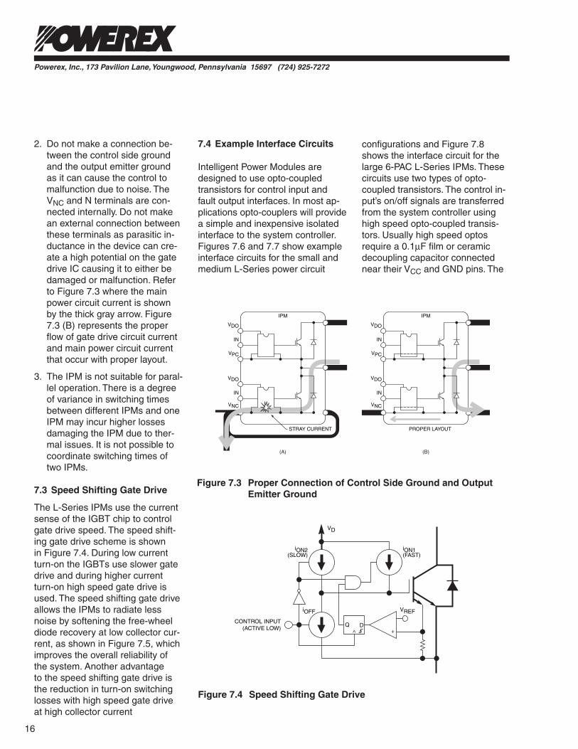
2. Do not make a connection be-tween the control side ground and the output emitter ground as it can cause the control to malfunction due to noise. The VNC and N terminals are con-nected internally. Do not make an external connection between these terminals as parasitic in-ductance in the device can cre-ate a high potential on the gate drive IC causing it to either be damaged or malfunction. Refer to Figure 7.3 where the main power circuit current is shown by the thick gray arrow. Figure 7.3 (B) represents the proper flow of gate drive circuit current and main power circuit current that occur with proper layout.
3. The IPM is not suitable for paral-lel operation. There is a degree of variance in switching times between different IPMs and one IPM may incur higher losses damaging the IPM due to ther-mal issues. It is not possible to coordinate switching times of two IPMs.
7.3 Speed Shifting Gate Drive
The L-Series IPMs use the current sense of the IGBT chip to control gate drive speed. The speed shift-ing gate drive scheme is shown in Figure 7.4. During low current turn-on the IGBTs use slower gate drive and during higher current turn-on high speed gate drive is used. The speed shifting gate drive allows the IPMs to radiate less noise by softening the free-wheel diode recovery at low collector cur-rent, as shown in Figure 7.5, which improves the overall reliability of the system. Another advantage to the speed shifting gate drive is the reduction in turn-on switching losses with high speed gate drive at high collector current
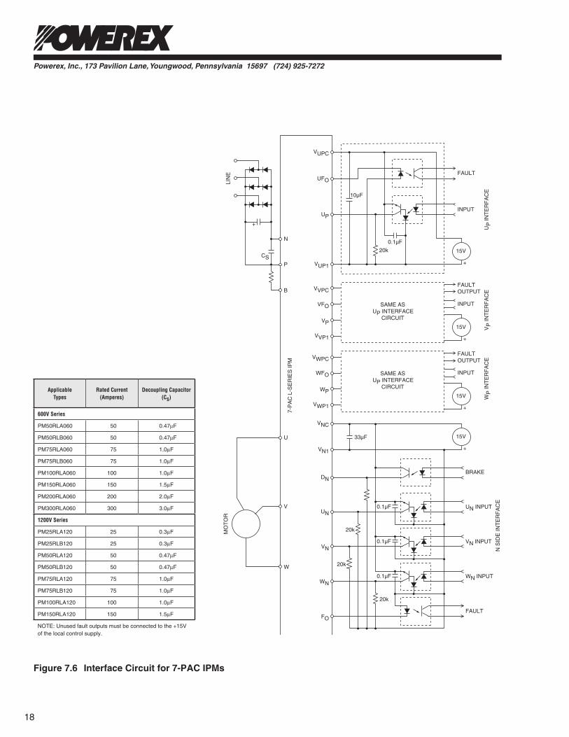
7.4 Example Interface Circuits
Intelligent Power Modules are designed to use opto-coupled transistors for control input and fault output interfaces. In most ap-plications opto-couplers will provide a simple and inexpensive isolated interface to the system controller. Figures 7.6 and 7.7 show example interface circuits for the small and medium L-Series power circuit
configurations and Figure 7.8 shows the interface circuit for the large 6-PAC L-Series IPMs. These circuits use two types of opto- coupled transistors. The control in-put’s on/off signals are transferred from the system controller using high speed opto-coupled transis-tors. Usually high speed optos require a 0.1µF film or ceramic decoupling capacitor connected near their VCC and GND pins. The
VDO
IPM
VPC
IN
VDO
VNC
IN
STRAY CURRENT
VDO
IPM
VPC
IN
VDO
VNC
IN
PROPER LAYOUT
(A) (B)
Figure 7.3 Proper Connection of Control Side Ground and Output Emitter Ground
VD
iON2(SLOW)
iOFF
CONTROL INPUT(ACTIVE LOW) DQ
^
iON1(FAST)
VREF
+
Figure 7.4 Speed Shifting Gate Drive

Powerex, Inc., 173 Pavilion Lane, Youngwood, Pennsylvania 15697 (724) 925-7272
17
1.5ms long fault output signal will be almost unaffected by the addi-tion of this filter. Always follow the interface circuit layout guidelines given in Section 7.2 when design-ing interface circuits.
7.5 Connecting the Interface Circuit
The input pins of Powerex Intel-ligent Power Modules are designed to be connected directly to a printed circuit board. Noise pick up can be minimized by building the interface circuit on the PCB near the input pins of the module. The control pins are designed to be connected to the PCB using an inverse mounted header recep-tacle. This connection technique, as shown in Figure 7.9, can also be adapted to large 6-PAC and 7-PAC modules. Table 7.2 shows the suggested connection method and connector for L-Series IPMs. Figures 7.10 and 7.11 show the PCB layout for L-Series and the connectors listed on the table.
7.6 Dead Time (tDEAD)
In order to prevent arm shoot through a dead time between high and low side input on signals is required in the system control logic. It is important to consider opto- coupler delay times when setting the controller’s dead time.
7.7 Using the Fault Signal
In order to keep the interface cir-cuits simple the Intellimod uses a single on/off output to alert the sys-tem controller of all fault conditions. The system controller can easily determine whether the fault signal
START 30 MHz 10 MHz/ STOP 130 MHz
START 30 MHz 10 MHz/ STOP 130 MHz
100
90
60
70
80
60
70
80
90
100
5th GEN.
PM50RLA060
VER:10dB/DIV.(RELATIVE VALUE)HOR:10MHz/DIV.
4th GEN.
PM50RSD060
speed opto-coupled transistors can be used for the fault output and brake input. Slow optos have the added advantages of lower cost and higher current transfer ratios. The example interface circuits use an NEC PS2501 low speed opto-coupled transistor for the transfer of brake and fault signals. Like most low speed opto-couplers the PS2501 does not have internal shielding. Some switching noise will be coupled through the opto-coupler. Other recommended low speed opto-coupler types are the PS2502 (NEC) and the TLP-521 (Toshiba). An RC filter with a time constant of about 10µs can be added to the opto’s output to remove this noise. The IPM’s
value of the control input pull up resistor is selected low enough to avoid noise pick up by the high impedance input and high enough so that the high speed opto- transistor with its relatively low current transfer ratio can still pull the input low enough to assure turn on. The circuits shown use an Avago HCPL-4504 opto-transistor. This opto was chosen mainly for its high common mode transient im-munity of 15,000V/µs. For reliable operation in IGBT power circuits opto-couplers should have a minimum common mode noise im-munity of 10,000 V/µs. The HCPL-4506, PS9613 (NEC) and TLP559 (Toshiba) are other recommended high speed opto-coupler types. Low
Figure 7.5 Noise Reduction Ver:10dB/div.
Powerex, Inc., 173 Pavilion Lane, Youngwood, Pennsylvania 15697 (724) 925-7272
18
MO
TO
R
7-P
AC
L-S
ER
IES
IPM
LIN
E
10µF
0.1µF
SAME ASUP INTERFACE
CIRCUIT
20k
FAULT
INPUT
FAULTOUTPUT
INPUT
15V
+
15V
+
+
CS
B
U
V
W
P
N
UP
VUP1
VVPC
VFO
VP
VVP1
VWPC
WFO
WP
VWP1
VNC
VN1
DN
UN
VN
WN
FO
UFO
VUPC
SAME ASUP INTERFACE
CIRCUIT
FAULTOUTPUT
INPUT
15V
+
15V
+
UP
INT
ER
FA
CE
VP
INT
ER
FA
CE
WP
INT
ER
FA
CE
N S
IDE
INT
ER
FA
CE
33µF
BRAKE
UN INPUT0.1µF
VN INPUT0.1µF
WN INPUT0.1µF
FAULT
20k
20k
20k
Applicable Types
Rated Current (Amperes)
Decoupling Capacitor (CS)
600V Series
PM50RLA060 50 0.47µF
PM50RLB060 50 0.47µF
PM75RLA060 75 1.0µF
PM75RLB060 75 1.0µF
PM100RLA060 100 1.0µF
PM150RLA060 150 1.5µF
PM200RLA060 200 2.0µF
PM300RLA060 300 3.0µF
1200V Series
PM25RLA120 25 0.3µF
PM25RLB120 25 0.3µF
PM50RLA120 50 0.47µF
PM50RLB120 50 0.47µF
PM75RLA120 75 1.0µF
PM75RLB120 75 1.0µF
PM100RLA120 100 1.0µF
PM150RLA120 150 1.5µF
NOTE: Unused fault outputs must be connected to the +15V of the local control supply.
Figure 7.6 Interface Circuit for 7-PAC IPMs

Powerex, Inc., 173 Pavilion Lane, Youngwood, Pennsylvania 15697 (724) 925-7272
19
6-PA
C L
-SE
RIE
S IP
M
U
V
W
P
N
UP
VUP1
VVPC
VFO
VP
VVP1
VWPC
WFO
WP
VWP1
VNC
VN1
UN
VN
WN
FO
VUPC
LIN
E
10µF
0.1µF
SAME ASUP INTERFACE
CIRCUIT
20k
FAULT
INPUT
FAULTOUTPUT
INPUT
15V
15V
+
CS
SAME ASUP INTERFACE
CIRCUIT
FAULTOUTPUT
INPUT
15V
+
15V
+
UP
INT
ER
FAC
EV
P IN
TE
RFA
CE
WP
INT
ER
FAC
E
33µF
MO
TOR
N S
IDE
INT
ER
FAC
E
UN INPUT0.1µF
VN INPUT0.1µF
WN INPUT0.1µF
FAULT
20k
20k
20k
+
+
UFO
Applicable Types
Rated Current (Amperes)
Decoupling Capacitor (CS)
600V Series
PM50CLA060 50 0.47µF
PM50CLB060 50 0.47µF
PM75CLA060 75 1.0µF
PM75CLB060 75 1.0µF
PM100CLA060 100 1.0µF
PM150CLA060 150 1.5µF
PM200CLA060 200 2.0µF
PM300CLA060 300 3.0µF
1200V Series
PM25CLA120 25 0.3µF
PM25CLB120 25 0.3µF
PM50CLA120 50 0.47µF
PM50CLB120 50 0.47µF
PM75CLA120 75 1.0µF
PM75CLB120 75 1.0µF
PM100CLA120 100 1.0µF
PM150CLA120 150 1.5µF
NOTE: If high side fault outputs are not used, they must be connected to the +15V of the local power supply.
Figure 7.7 Interface Circuit for 6-PAC IPMs

Powerex, Inc., 173 Pavilion Lane, Youngwood, Pennsylvania 15697 (724) 925-7272
20
FAULTOUTPUT
FAULTOUTPUT
VP
INT
ER
FAC
EW
P IN
TE
RFA
CE
FAULTOUTPUT
FAULTOUTPUT
UN
INT
ER
FAC
EV
N IN
TE
RFA
CE
FAULTOUTPUT
WN
INT
ER
FAC
E
FAULT
INPUT
UP
INT
ER
FAC
E
15V
15V
15V
15V
+
+
+
+
15V
+
15V
+
SAME ASUP INTERFACE
CIRCUIT
SAME ASUP INTERFACE
CIRCUIT
SAME ASUP INTERFACE
CIRCUIT
SAME ASUP INTERFACE
CIRCUIT
6-PA
C L
-SE
RIE
S IP
M
U
V
W
P
N
UP
VUP1
VVPC
VPFO
VP
VVP1
VWPC
WPFO
WP
VWP1
VUNC
UNFO
VUN1
VVNC
VWNC
VNFO
VN
VVN1
WN
WNFO
VWN1
UPFO
VUPC
LIN
E
10µF
0.1µF
20kCS
MO
TOR
+
SAME ASUP INTERFACE
CIRCUIT
INPUT
INPUT
INPUT
INPUT
INPUT
Applicable Types
Rated Current (Amperes)
Decoupling Capacitor (CS)
600V Series
PM450CLA060 450 µF
PM600CLB060 600 µF
1200V Series
PM200CLA120 200 µF
PM300CLA120 300 µF
PM450CLA120 450 µF
PM600CLA120 600 µF
NOTE: If high side fault outputs are not used, they must be connected to the +15V of the local power supply.
Figure 7.8 Interface Circuit for 6-PAC IPMs

Powerex, Inc., 173 Pavilion Lane, Youngwood, Pennsylvania 15697 (724) 925-7272
21
L-SERIES IPM
PRINTED CIRCUITBOARD
GUIDE PIN CONTROL PINS INVERSE HEADER RECEPTACLE
Figure 7.9 Connecting the Interface Circuit to the IPM
F
G
DB
CE
H
A
G
Part Dia. A Distance from First Center of Guide Pin to Center of Last Guide Pin 2.75" B Hole for Header Receptacle Pin 0.032" C Clearance Hole for Intellimod Pin 0.032" D Clearance Hole for Intellimod Guide Pin 0.110" E Intellimod Pin Spacing 0.100" F Intellimod IGBT Ground Pin Spacing 0.630" G Guide Pin to First Intellimod P.S. Pin Spacing 0.130"H Spacing Between Header Receptacle Pin and Intellimod Pin 0.100"
Part Dia. A Distance from Center of First Guide Pin to Center of Last Guide Pin 5.19" B Distance from Center of Intellimod Pin to Center of Intellimod Pin 4.94"C Distance between Guide Pin Centers Enclosing a Connector 1.25"D Distance between Proximate Guide Pin Centers Enclosing Adjacent Connectors 0.72"E Intellimod Pin Spacing 0.1"F Distance from First Pin Column to Fifth Pin Column 0.7"G Distance from First Pin of One Connector to first Pin of Next Connector 1.974"H Clearance Hole for Intellimod Guide Pin 0.11"J Clearance Hole for Intellimod Pin 0.04"K Hole for Header Receptacle Pin 0.04"
A
CC D
FE E E
G
B
D C
E
K
JH
Figure 7.10 L-Series Intelligent Power Module Type Connection Method Using DF10-31S-2DSA (59)
Figure 7.11 L-Series Intelligent Power Module Type Connection Method Using MDF7-11S-2.54DSA (22)
tem controller of all fault conditions. The system controller can easily determine whether the fault signal was caused by an over tempera-ture or over-current/short-circuit by examining its duration. Short-circuit and over-current condition fault signals will be tFO (nominal 1.5ms) in duration. An over-temperature fault signal will be much longer. The over-temperature fault starts when the baseplate temperature exceeds the OT level and does not reset until the baseplate cools below the OTR level. Typically this takes tens of seconds.
NOTE: Unused fault outputs must be properly terminated by con-necting them to the +15V on the local control power supply. Failure to properly terminate unused fault outputs may result in unexpected tripping of the modules internal protection.
7.8 IPM Inverter Examples
The IPM’s integrated intelligence greatly simplifies inverter design. The built in protection circuits al-low maximum utilization of power device capability without compro-mising reliability. Input common mode noise filtering and MOV surge suppression helps to protect the input rectifier and IPMs from line transients. The main power bus is constructed using parallel plates separated by a thin layer of elec-trical insulation material in order to minimize parasitic inductance. Low inductance bus designs are covered in more detail in the Gen-eral Application notes for IGBTs. The IPMs must be mounted on a heatsink with suitable cooling capa-bilities. Thermal design and power loss equations are covered in of the General Application notes for IGBTs. The following section of this application note gives an overview

Powerex, Inc., 173 Pavilion Lane, Youngwood, Pennsylvania 15697 (724) 925-7272
22
of our on-line simulator that greatly simplifies power loss and junction temperature calculations. Powerex offers a complete line-up of diode modules that are ideal for use as the input bridge in inverter applica-tions.
8.0 Power Loss and Junction Temperature Calculations
The Mitsubishi Average Loss Simu-lation Software is a very powerful tool for estimating power loss and can be used with all of the L-Series IPM modules. The Powerex home page contains a link to the soft-ware.
The following steps take you through an example calculation
Application conditions are as follows:
Icp: Peak Collector Current VCC: Bus Voltage Fsw: Switching Frequency Tf: Heatsink Temperature Rg: Resistivity of Gate Resistor PF: Power Factor
8. Hit the equal icon in the tool bar.
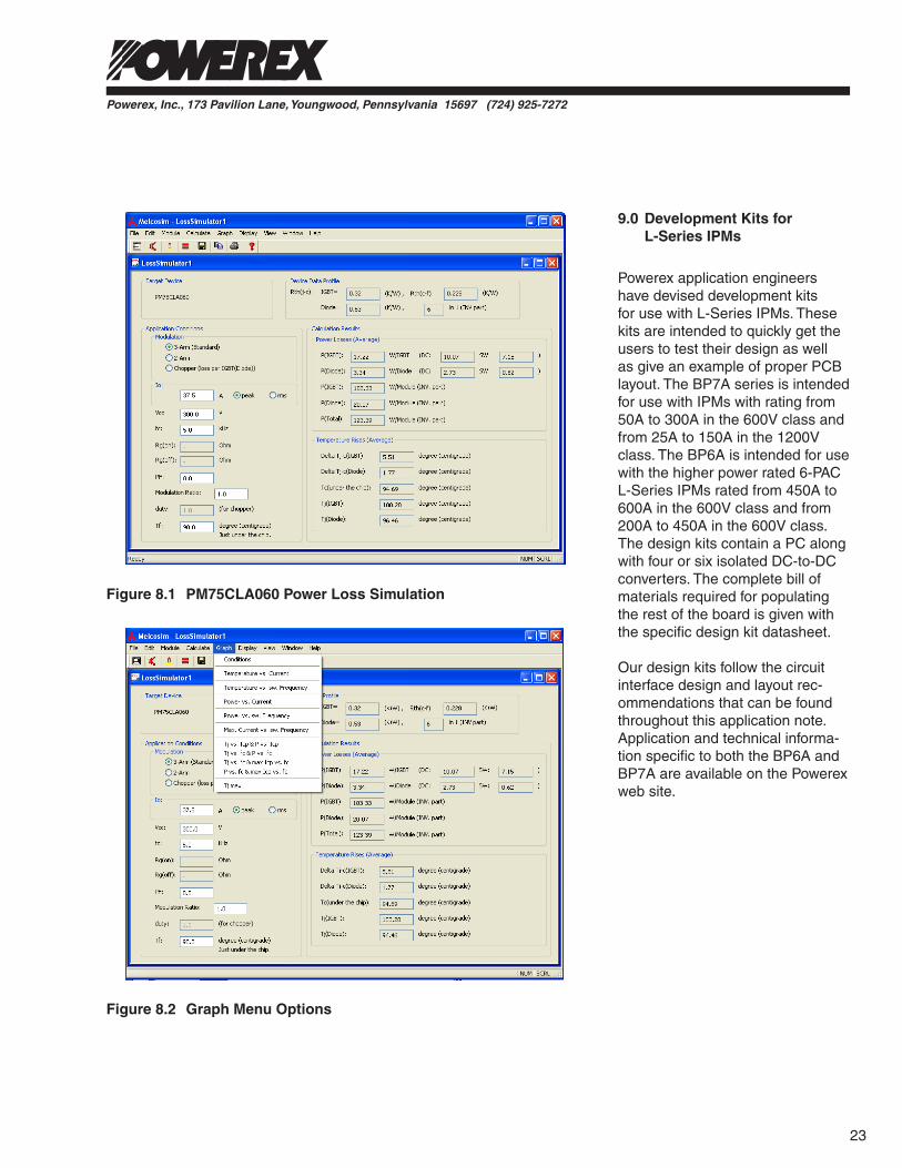
Simulator results for the PM75CLA060 are shown in Figure 8.1.
The initial results displayed by the simulator are a steady state approximation and are as follows:
Tj (IGBT): Chip junction tempera-ture for the IGBT Tj (Diode): Chip junction tempera-ture for the free-wheeling diode P(IGBT): Power loss by each IGBT P(Diode): Power loss by each diode P(Total): Sum of power loss from all diode and IGBTs in the module
Once the simulator has made power loss calculations, you can choose a variety of power loss curves from the Graph menu in the tool bar as shown in Figure 8.2.
Figure 8.3 shows total power dis-sipation versus switching frequency while Figure 8.4 shows total power dissipation versus collector current for the PM75CLA060. Both graphs have separate curves for IGBT and diode losses.
estimating losses with a PM75CLA060 using the simulator:
1. Start the simulation software,
2. Click on the IGBT icon in the tool bar.
3. Select IPM from the division pull down menu.
4. Select IPM L-Series from the series pull down menu.
5. Select PM75CLA060 from the module pull down menu.
6. Click the Ok button
7. Enter the application conditions. (Typical application conditions for the device will be entered as a default.)
Table 7.2 L-Series Connection Methods
Part NumberCurrent
(A)Voltage
(V)Brake Current
(A)Connector
(Hirose Part Number)
PM50(#)L(*)060 50 600 30 DF10-31S-2DSA (59)
PM75(#)L(*)060 75 600 50 DF10-31S-2DSA (59)
PM100(#)LA060 100 600 50 DF10-31S-2DSA (59)
PM150(#)LA060 150 600 75 DF10-31S-2DSA (59)
PM200(#)LA060 200 600 100 DF10-31S-2DSA (59)
PM300(#)LA060 300 600 150 DF10-31S-2DSA (59)
PM450CLA060 450 600 NA MDF7-11S-2.54DSA (22)
PM600CLA060 600 600 NA MDF7-11S-2.54DSA (22)
PM25(#)L(*)120 25 1200 15 DF10-31S-2DSA (59)
PM50(#)L(*)120 50 1200 25 DF10-31S-2DSA (59)
PM75(#)L(*)120 75 1200 40 DF10-31S-2DSA (59)
PM100(#)LA120 100 1200 50 DF10-31S-2DSA (59)
PM150(#)LA120 150 1200 75 DF10-31S-2DSA (59)
PM200CLA120 200 1200 NA MDF7-11S-2.54DSA (22)
PM300CLA120 300 1200 NA MDF7-11S-2.54DSA (22)
PM450CLA120 450 1200 NA MDF7-11S-2.54DSA (22)
(*) Package Options: B = Solder Pin, A = Screw Terminal (#) Circuit Options: R = 7-PAC (6-PAC + Brake), C = 6-PAC EXAMPLE: PM75RLB120 is a 75A, 1200V, 7-PAC (6-PAC + Brake) in a Solder Pin Package
Powerex, Inc., 173 Pavilion Lane, Youngwood, Pennsylvania 15697 (724) 925-7272
23
9.0 Development Kits for L-Series IPMs
Powerex application engineers have devised development kits for use with L-Series IPMs. These kits are intended to quickly get the users to test their design as well as give an example of proper PCB layout. The BP7A series is intended for use with IPMs with rating from 50A to 300A in the 600V class and from 25A to 150A in the 1200V class. The BP6A is intended for use with the higher power rated 6-PAC L-Series IPMs rated from 450A to 600A in the 600V class and from 200A to 450A in the 600V class. The design kits contain a PC along with four or six isolated DC-to-DC converters. The complete bill of materials required for populating the rest of the board is given with the specific design kit datasheet.
Our design kits follow the circuit interface design and layout rec-ommendations that can be found throughout this application note. Application and technical informa-tion specific to both the BP6A and BP7A are available on the Powerex web site.
Figure 8.2 Graph Menu Options
Figure 8.1 PM75CLA060 Power Loss Simulation

Powerex, Inc., 173 Pavilion Lane, Youngwood, Pennsylvania 15697 (724) 925-7272
24
Figure 8.4 PM75CLA060 Total Power Loss Versus IC
Figure 8.3 PM75CLA060 Total Power Loss Versus Switching Frequency