ksa mos ultrascan - k-space · pdf fileksa mos ultrascan ksa mos ultrascan is a flexible,...
TRANSCRIPT

kSA MOS UltraScan
kSA MOS UltraScan is a flexible, high-resolution scanning curvature, stress, thickness, tilt, and absolute reflectance measurement system. Based on the proven technology of our standard in situ kSA MOS system, it simultaneously measures the sample curvature in two orthogonal directions using a two-dimensional laser array. It performs high resolution XY scanning of semiconductor wafers, optical mirrors, lenses, or practically any polished surface.
kSA MOS UltraScan XY scanning provides uniform spatial scan resolution over the entire wafer/sample surface. Scans are fully programmable for line scans, selected area maps, and full area maps, perfect for circular, square or patterned samples. The system also provides quantitative film stress analysis by first scanning the sample and then re-scanning the sample post-process.
Measures:
Curvature
Bow Height
Thin Film Stress
Tilt
Absolute Reflectance
Film Thickness and Spectral Reflectance
(Optional)
Materials:
Wafers
Optical Mirrors
Lenses
Glass
Polished/Smooth Surfaces
kSA MOS UltraScan
Flexible, High-Resolution Curvature, Stress, Thickness, and Reflectance Mapping, All in One Tool!
k-Space Associates, Inc. | T: 734.426.7977 | [email protected] | k-space.com

kSA MOS: The kSA Multi-beam Optical Sensor, or kSA MOS, technology is based on a patented approach which uses a single laser to generate a two-dimensional laser array. This laser spot array is then reflected off the sample surface into a high-resolution CCD detector. Changes in the reflected laser array spot spacing at each point on the sample are used to determine the localized sample curvature in both the X and Y direction. In this way, the system directly measures the curvature and stress in two dimensions simultaneously. This is something that single or dual beam curvature and stress tools simply cannot capture.
Simultaneous detection of the laser array also makes the measurement inherently less sensitive to sample vibration compared with systems that rely on scanning the laser spot on the surface of the sample to measure the local curvature. This leads to kSA MOS’s increased curvature resolution capability. Since all the laser spots move together at the same frequency, movement or tilt is not incorrectly detected as a change in sample curvature.
XY Scanning: kSA MOS UltraScan is equipped with XY scanning over a 300mm x 300mm area. This provides the advantage of uniform spatial data resolution over the entire sample. At large diameters spatial resolution will not be lost, which is typically a problem in linear scanning systems with rotation stages. It also provides easy measurement set up for rectangular samples or for mapping limited areas of a sample.
Curvature: kSA MOS UltraScan is equipped with both flat and curved reference mirrors for quick and easy curvature calibration. The curvature of your sample is measured directly from the laser spot spacing, resulting in high accuracy single point and scanning curvature measurements. Using sophisticated image processing and data analysis algorithms, the kSA MOS UltraScan can easily detect sub-micron changes in spot position due to
kSA MOS UltraScan Measurement Technologies
kSA MOS UltraScan curvature surface plot of a commercial GaN on sapphire template.
2 k-Space Associates, Inc. | T: 734.426.7977 | [email protected] | k-space.com
kSA MOS UltraScan
kSA MOS UltraScan reflectance map of a commercial GaN on sapphire template.

changes in sample curvature. This makes it the highest curvature and stress resolution metrology tool available.
Absolute Reflectance: Absolute reflectance of the sample at the laser wavelength is determined by measuring the integrated intensity of the laser spots on the CCD detector, and is automatically calibrated before each scan by using the integrated flat mirror. This provides useful information about the quality and uniformity of the sample surface, as well as interference effects for film stacks.
Bow Height: When a laser is reflected off a bowed sample, the reflected angle will differ at different points on the sample. The automated laser tracking in the kSA MOS UltraScan optics not only keeps the laser array centered on the detector but also measures the changes in the angle of reflection of the laser array in order to determine the local sample bow height and surface tilt angle.
Film Stress: To generate a thin-film stress map of a sample, the local curvature of the sample must be determined both pre- and post-deposition. The point-by-point thin-film stress is determined based on the change in the point-by-point curvature from the pre- and post-process curvature maps, as well as the substrate thickness, the biaxial modulus of the substrate and the film thickness. The changes in stress of a thin film after processing may also be determined from the curvature maps measured after the subsequent processing steps.
Spectral Reflectance and Film Thickness (optional add-on): This option equips the kSA MOS UltraScan optics with a light source and a fiber coupled spectrometer. This allows the spectral reflectance of the sample to be measured at each point on the sample. Using kSA’s proprietary software to measure the extrema positions in the spectral reflectance spectra, the kSA MOS UltraScan can determine the point-by point thickness of semitransparent thin films on a substrate. This data can be mapped along with other measurement parameters such as wafer curvature and film stress. Alternatively, the spectral reflectance data can be exported for multi-layer thickness or device modeling in other software programs.
k-Space Associates, Inc. | T: 734.426.7977 | [email protected] | k-space.com 3
kSA MOS UltraScan
kSA MOS UltraScan thickness contour plot of a commercial GaN on sapphire template.
kSA MOS UltraScan bow height surface plot of a commercial GaN on sapphire template.

kSA MOS UltraScan Models Standard Package
Model Description
kSA MOS UltraScan MOS-US
Complete curvature, film stress, tilt, bow, and absolute 660nm reflectance measurements as function of sample position. System includes:
- Standard CCD detector, laser, optics, servo-motor mirror controller, computer controller, kSA software, complete steel frame enclosure with lockable wheels, and uninterruptable UPS power supply with voltage regulation
- Built-in flat and 10m radius of curvature reference mirrors - Standard sample holder for 50mm, 75mm, 100mm, 150mm, 200mm,
and 300mm diameter samples - Fully programmable XY scanning stage with options for line scans,
selected area mapping, and full area mapping - kSA 2-D and 3-D mapping and analysis software - One kSA analysis only software license (M-AOS) for offline data analysis
on a separate computer
Options
Options Description
NIR Spectral Reflectance and Film Thickness Module M-SR-1670/U
Provides additional integrated hardware for absolute spectral reflectance measurement in the range of 870-1670nm with an integrated software module for the calculation of total film thickness.
Large Format Camera M-HRD/U
Larger format and higher resolution CCD detector for applications with large convex curvature and/or a large degree of wafer bow.
405 nm Laser and Optics M-405/U
Replaces the standard laser and optics in the MOS-US with a 405nm laser and suitable optics for greater surface sensitivity.
4” Optics M-4inch/U
Replaces standard optics with 4” optics to accommodate a large degree of wafer bow on large wafers/samples.
Custom Sample Holders Custom sized sample holders available and quoted separately. - Examples: 10mm x 10mm square samples, flat insert for odd sized
samples, etc.
Custom Large Area Panel Scanning Custom scanning systems from 300mm x 300mm up to 2m x 2m samples.
Large Diameter Mirror Curvature Mapping (up to 1.5m diameter)
See kSA MegaMOS Product Specification for details.
Thermal Process Chamber Allows for curvature and stress mapping as a function of temperature. See kSA MOS ThermalScan Product Specifications for details.
kSA MOS UltraScan
4 k-Space Associates, Inc. | T: 734.426.7977 | [email protected] | k-space.com
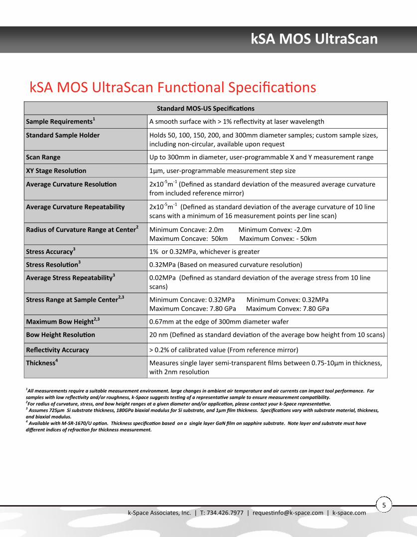
kSA MOS UltraScan Functional Specifications Standard MOS-US Specifications
Sample Requirements1 A smooth surface with > 1% reflectivity at laser wavelength
Standard Sample Holder Holds 50, 100, 150, 200, and 300mm diameter samples; custom sample sizes, including non-circular, available upon request
Scan Range Up to 300mm in diameter, user-programmable X and Y measurement range
XY Stage Resolution 1µm, user-programmable measurement step size
Average Curvature Resolution 2x10⁻⁵m-1 (Defined as standard deviation of the measured average curvature from included reference mirror)
Average Curvature Repeatability 2x10⁻⁵m-1 (Defined as standard deviation of the average curvature of 10 line scans with a minimum of 16 measurement points per line scan)
Radius of Curvature Range at Center2 Minimum Concave: 2.0m Minimum Convex: -2.0m Maximum Concave: 50km Maximum Convex: - 50km
Stress Accuracy3 1% or 0.32MPa, whichever is greater
Stress Resolution3 0.32MPa (Based on measured curvature resolution)
Average Stress Repeatability3 0.02MPa (Defined as standard deviation of the average stress from 10 line scans)
Stress Range at Sample Center2,3 Minimum Concave: 0.32MPa Minimum Convex: 0.32MPa Maximum Concave: 7.80 GPa Maximum Convex: 7.80 GPa
Maximum Bow Height2,3 0.67mm at the edge of 300mm diameter wafer
Bow Height Resolution 20 nm (Defined as standard deviation of the average bow height from 10 scans)
Reflectivity Accuracy > 0.2% of calibrated value (From reference mirror)
Thickness4 Measures single layer semi-transparent films between 0.75-10µm in thickness, with 2nm resolution
1All measurements require a suitable measurement environment. large changes in ambient air temperature and air currents can impact tool performance. For samples with low reflectivity and/or roughness, k-Space suggests testing of a representative sample to ensure measurement compatibility. 2For radius of curvature, stress, and bow height ranges at a given diameter and/or application, please contact your k-Space representative. 3 Assumes 725µm Si substrate thickness, 180GPa biaxial modulus for Si substrate, and 1µm film thickness. Specifications vary with substrate material, thickness, and biaxial modulus. 4 Available with M-SR-1670/U option. Thickness specification based on a single layer GaN film on sapphire substrate. Note layer and substrate must have different indices of refraction for thickness measurement.
kSA MOS UltraScan
k-Space Associates, Inc. | T: 734.426.7977 | [email protected] | k-space.com 5

kSA MOS UltraScan System Specifications
10
16
mm
4
47
mm
701mm
12
20
mm
2
57
mm
Sample Holder: Wafer holder machined from solid aluminum block for mechanical stability. The standard stage holds 50, 75, 100, 150, 200, and 300mm diameter samples. Stage is equipped with both a flat reference and a 10m radius of curvature mirror for automated, easy, and reproducible system calibration. Custom sample holders quoted separately.
kSA MOS UltraScan
System Frame: A robust welded steel frame houses the entire wafer holder, control electronics, and metrology system, so there is no need for an expensive vibration isolation table to house this stand alone unit. The frame has retractable castors so that the system can rest on vibration isolation pads if desired.
Flat Mirror
X tilt adjustment
Y tilt adjustment 300mm
200mm
150mm
100mm 75mm 50mm
10m ROC Mirror
6 k-Space Associates, Inc. | T: 734.426.7977 | [email protected] | k-space.com

Controller: The kSA MOS UltraScan system is supplied with a fully configured, Windows 7, multi-core CPU, A4 rack mounted computer system with a 22” LCD Monitor on a frame mounted swing arm. Please refer to the kSA Computer Product Specifications for the latest computer configuration. k-Space does not recommend or encourage customers to substitute or update their own computer for the kSA supplied controller. The kSA MOS UltraScan system uses several data acquisition boards that require specific bus slots and additional I/O slots on the back plane of the computer chassis. Facility Requirements System Power: 110 or 220V; at 220V the unit draws 3 - 4A. System Dimensions: W=70cm L=101.6cm H= 156cm to 160cm, depending on feet adjustment. Sample drawer extends an additional 45cm when opened. Monitor arm can attach to the left or right side, and extends to side. System Weight: 295kg (650lbs).
kSA MOS UltraScan
Photograph of kSA MOS UltraScan with MOS optics, scanning stage and sample holder exposed.
k-Space Associates, Inc. | T: 734.426.7977 | [email protected] | k-space.com 7

Detectors The MOS UltraScan system utilizes a CCD detector (K1400-12) for imaging of the laser array. A larger format, high resolution detector (K3300-14)may be required for some applications.
Lasers The kSA MOS UltraScan system utilizes fiber-coupled, Peltier-cooled laser diode packages with integrated current controller and temperature controller for generating the laser array. A different laser wavelength and associated optics may be required/desirable for some applications. Note: All high-power beams are confined within the kSA MOS UltraScan housing even when the cover is removed for alignment. The cover is not interlocked, but may be upon request. Direct access to the main beam is necessary during alignment.
660 nm ( MOS-US Standard ) 405 nm (with M-405/U)
Operation Mode Constant current Constant Current
Spot Size ~ 0.8mm spot diameter, typical array is 6x4mm (4x3 spot array)
~ 0.8mm spot diameter, typical array is 6x4mm (4x3 spot array)
Power > 70mW (<10µW exits the optical enclosure)
> 50mW (<10µW exits the optical enclosure)
Stability ≤ 0.2% ≤ 0.2%
Lifetime 10,000 hours (mean time before failure), 1 year warranty
10,000 hours (mean time before failure), 1 year warranty
kSA MOS UltraScan
Standard Detector Large Format Detector (with M-HRD/U)
Model K1400-12 K3300-14
CCD Format 2/3” type, Sony ICX285 Progressive scan 4/3 type, KAI-08050 Progressive scan
Resolution 1360 x 1024 pixels (1.4MP) 3296 x 2472 pixels (8MP)
Pixel size 6.45µm 5.5µm
Sensing area 8.8mm x 6.6mm 18.13mm x 13.6mm
Bit depth 12-bit 14-bit
Dynamic Range 58dB 62dB
Exposure time Variable from 10µs to 77.3s Variable from 10µs to 26.8s
Output format GigE GigE
Power 12V DC (internal from computer) or external 120/240V
12V DC (internal from computer) or external 120/240V
8 k-Space Associates, Inc. | T: 734.426.7977 | [email protected] | k-space.com
kSA MOS UltraScan Analysis Only Software Sentinel Key M-AOS option is an analysis-only software sentinel key that allows complete kSA MOS UltraScan functionality, with the exception of data acquisition. It is designed for users who want to perform post acquisition, display, processing and analysis away from the laboratory. Installation and Training A minimum of 1-2 days of on-site customer installation are required with system purchase. Warranty All kSA systems and integrated components are warranted against defective materials and workmanship for a period of ONE YEAR from the date of delivery to the original purchaser.
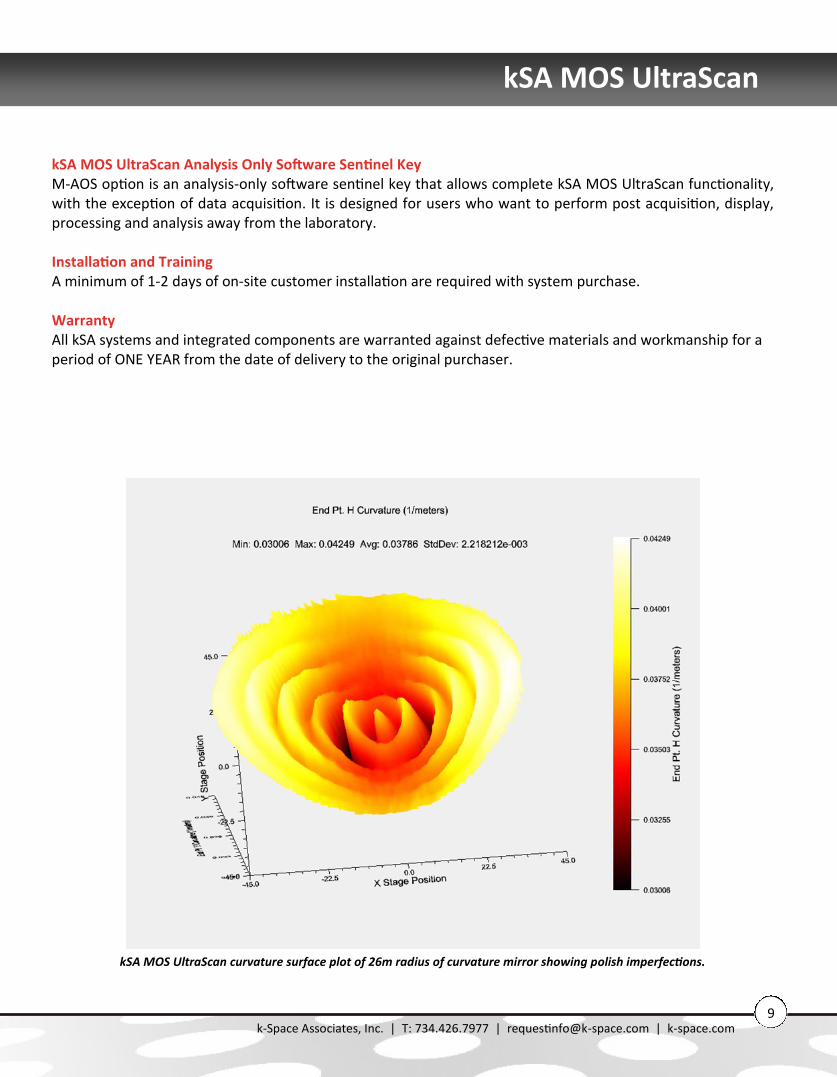
kSA MOS UltraScan
kSA MOS UltraScan curvature surface plot of 26m radius of curvature mirror showing polish imperfections.
k-Space Associates, Inc. | T: 734.426.7977 | [email protected] | k-space.com 9

The kSA MOS UltraScan software controls and monitors all applicable hardware including laser, CCD detector, servo-motor control mirror, XY scanning stage, and data acquisition boards. The software automatically detects the laser array, controls the CCD detector exposure time to ensure no saturation as the surface reflectivity changes, and continuously centers the reflected array via real-time adjustment of the servo-controlled fold mirror as the sample is scanned.
The kSA MOS UltraScan software provides real-time plotting of differential spot spacing, curvature, reflectivity, bow height, film stress, film thickness (optional), and spectral reflectance (optional). Scanning recipes may be saved for easy measurement setup. For system calibration, the kSA MOS UltraScan automatically measures the calibration mirrors before sample scanning for fast, easy, and consistent calibration run after run. The multithreaded architecture of the kSA MOS UltraScan software allows you to analyze previously acquired data while a current scan is being performed. In addition, the complementary analysis only software license allows the user to analyze data at a separate location, if needed.
All kSA metrology software has a user-friendly Windows-standard environment with extensive error checking and file handling. It is user configurable so that each user’s preferred window layouts and acquisition/analysis preferences can be saved for future use. kSA metrology software allows data storage in ASCII, Excel or binary file formats, facilitating alternative data analysis if desired. Included in all kSA metrology software are high-quality 2D and 3D graphics for data display and analysis, as well as numerous image and graphics editing capabilities, including false coloring using pre-loaded or user-defined color palettes, and label editing. Transport graphics directly to the Windows clipboard, or export to wmf, png, tiff, or bmp formats. For integration with other computer systems, complete TCP/IP interface for custom, real-time data transfer and program control, and data transfer to SQL databases is available.
kSA MOS UltraScan
kSA MOS UltraScan Integrated Software
kSA Software screen shot.
10 k-Space Associates, Inc. | T: 734.426.7977 | [email protected] | k-space.com
kSA MOS UltraScan
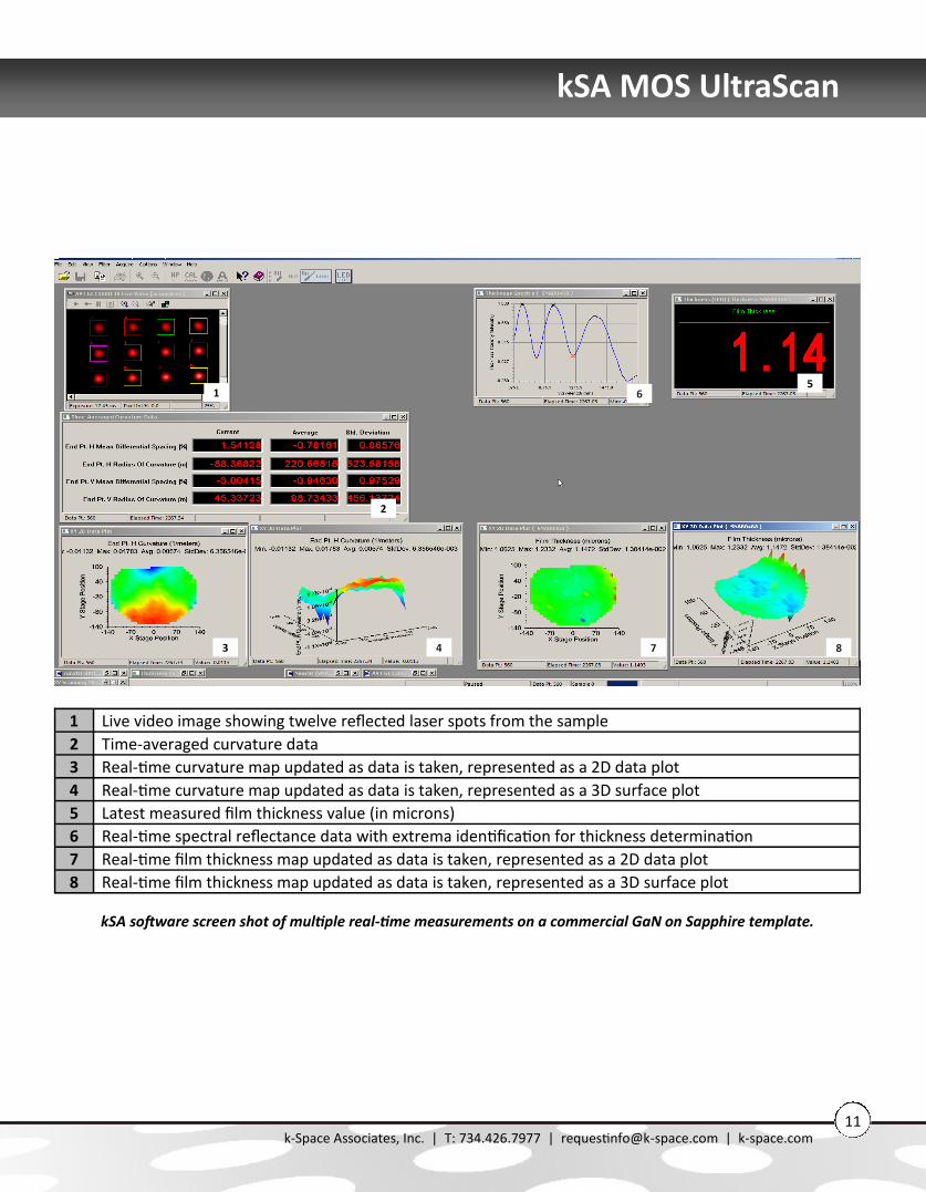
3
1
4
2
5 6
7 8
1 Live video image showing twelve reflected laser spots from the sample
2 Time-averaged curvature data
3 Real-time curvature map updated as data is taken, represented as a 2D data plot
4 Real-time curvature map updated as data is taken, represented as a 3D surface plot
5 Latest measured film thickness value (in microns)
6 Real-time spectral reflectance data with extrema identification for thickness determination
7 Real-time film thickness map updated as data is taken, represented as a 2D data plot
8 Real-time film thickness map updated as data is taken, represented as a 3D surface plot
kSA software screen shot of multiple real-time measurements on a commercial GaN on Sapphire template.
k-Space Associates, Inc. | T: 734.426.7977 | [email protected] | k-space.com 11

k-Space has an expansive network of distributors to best serve our worldwide customer base.
HEADQUARTERS
k-Space Associates, Inc. Michigan, USA www.k-space.com [email protected]
DISTRIBUTION PARTNERS
RTA Instruments Ltd. Europe www.rta-instruments.com [email protected]
Giant Force Technology Co., Ltd. China www.giantforce.cn [email protected]
R-DEC Co., Ltd. Japan, Hong Kong, Taiwan www.rdec.co.jp [email protected]
El Camino Technologies Pvt Ltd. India www.elcamino.in [email protected]
Jung Won Corporation South Korea www.jwc.co.kr [email protected]
Specifications are subject to change without notice. While due caution has been exercised in the production of this document, possi-
ble errors and omissions may occur.
k-Space Associates, Inc.
2182 Bishop Circle East Dexter, MI 48130 USA | T: 734.426.7977 | F: 734.426.7955 | request [email protected] | k-space.com
kSA MOS UltraScan Product Specs 29 Oct 15
kSA MOS UltraScan