ks0108 datasheet
TRANSCRIPT

SPECIFICATION
Model: LG128641-SFLYH6V

LG128641-SFLYH6V - 2 -
1. BASIC SPECIFICATIONS 1.1 Display Specifications
LCD Mode : STN Positive Transflective
Display Color : Dark Blue
Background Color : Yellow-Green
Driving Method : 1/64 Duty,1/9 Bias
Viewing Direction : 6:00
Backlight : LED
1.2 Mechanical Specifications
Outline Dimension : 78.0(W) X 70.0(H) X 13.0(T) mm
Viewing Area : 62.0(W) X 44.0(H) mm
Dot Matrix : 128 X 64 Dots
Dot Size : 0.40 X 0.55 mm
Dot Pitch : 0.44 X 0.60 mm
Weight : 75 g
1.3 Block Diagram
LCD PANEL
128 x 64 dots
DC/DCConverter
SS
DD
VV
OVOUTV
64 SEG 64 SEG
KS0107
or Eqv.
64 COM
KS0108or Eqv. or Eqv.
KS0108
DB7DB0RS, R/W, E, /RST
/CS2
LEDKLEDA
LED Backlight
/CS1

LG128641-SFLYH6V - 3 -
1.4 Terminal Functions
Pin No. Symbol Level Function
1 /CS1 L Chip Selection for IC1, Active “L”
2 /CS2 L Chip Selection for IC2, Active “L”
3 VSS - Ground
4 VDD - Power Supply for Logic (+5V)
5 VO - Power Supply for LCD
6 RS H/L Register Selection
H: Display Data L: Instruction Code
7 R/W H/L Read/Write Selection
H: Read Operation L: Write Operation
8 E H, H L Enable Signal. Read data when E is “H”, write
data at the falling edge of E.
9 DB0 H/L Data Bit0
10 DB1 H/L Data Bit1
11 DB2 H/L Data Bit2
12 DB3 H/L Data Bit3
13 DB4 H/L Data Bit4
14 DB5 H/L Data Bit5
15 DB6 H/L Data Bit6
16 DB7 H/L Data Bit7
17 /RST L Reset Signal, Active Low
18 VOUT -- Negative Voltage Output (-10V)
19 LEDA -- LED Power Supply (+5V)
20 LEDK -- LED Power Supply (0V)
2. ABSOLUTE MAXIMUM RATINGS
Item Symbol Min. Max. Unit
Supply Voltage(Logic) VDD-VSS -0.3 7.0 V
Supply Voltage(LCD) VDD-VO -0.3 19.0 V
Input Voltage VI -0.3 VDD+0.3 V
Operating Temp. Topr -20 70
Storage Temp. Tstg -30 80

LG128641-SFLYH6V - 4 -
3. ELECTRICAL CHARACTERISTICS 3.1 DC Characteristics (VDD=5.0V10%, Ta=25)
Item Symbol Condition Min. Typ. Max. UNIT
Supply Voltage
(Logic) VDD
4.5 5.0 5.5 V
Supply Voltage
(LCD Drive) VDD-VO
-- 12.0 -- V
Input High Voltage VIH 2.0 -- VDD V
Input Low Voltage VIL 0 -- 0.8 V
Output High Voltage VOH IOH=-0.2mA 2.4 -- VDD V
Output Low Voltage VOL IOL=1.6mA 0 -- 0.4 V
Supply Current
(Logic) IDD VDD=5.0V -- 6.0 8.0 V
3.2 Interface Timing Chart (VDD=5.0V10%, Ta=25)
Characteristic Symbol Min. Typ. Max. Unit
E Cycle tC 1000 -- -- ns
E High Level Width tWH 450 -- -- ns
E Low Level Width tWL 450 -- -- ns
E Rise Time tR -- -- 25 ns
E Fall Time tF -- -- 25 ns
Address Set-Up Time tASU 140 -- -- ns
Address Hold Time tAH 10 -- -- ns
Data Set-Up Time tDSU 200 -- -- ns
Data Delay Time tD -- -- 320 ns
Data Hold Time(Write) tDHW 10 -- -- ns
Data Hold Time(Read) tDHR 10 -- -- ns

LG128641-SFLYH6V - 5 -
t
t
tt t
t t
t t
t
E
R/W
DB0~DB7
RS
t
Fig.1 MPU Write Timing
DB0~DB7
RS
R/W
E
t
Fig.2 MPU Read Timing
t
t
t
t
t t
t
t t
t
C
WL
WHR F
ASU AH
ASU AH
DSUDSU
C
WL
R WH F
ASU AH
ASU AH
D DHR
/CS1, /CS2
/CS1, /CS2

LG128641-SFLYH6V - 6 -
3.3 LED Backlight Characteristics (Ta=25 )
Item Symbol Condition Min. Typ. Max. UNIT
Forward Voltage Vf 3.9 4.1 4.3 V
Forward Current If Vf=4.1V -- 300 -- mA
Peak Wave Length p If=300mA -- 568 -- nm
Luminance Lv If=300mA 50 -- -- cd/m2
3.4 Power Supply
+5V
+5V
VR20 k Ω VO LC
M
LEDK
LEDA
OUTV
VSS
VDD

LG128641-SFLYH6V - 7 -
4. OPERATING PRINCIPLES & METHODES 4.1 I/O Buffer
Input buffer controls the status between the enable and display of chip. Unless the /CS1
or /CS2 is in active mode, input or output of data and instruction does not execute.
Therefore internal state is not change. But /RST can operates regardless /CS1 or /CS2.
4.2 Input Register
Input register is provided to interface with MPU which operates in different frequency.
Input register stores the data temporarily before writing it into display data RAM.
When /CS1 or /CS2 is in the active mode, R/W and RS select the input register. The data
from MPU is written into input register, then into display data RAM. Data is latched at
falling edge of the E signal and then written into the display data RAM automatically by
internal operation.
4.3 Output Register
Output register stores the data temporarily which is read from display data RAM when
CS1 or CS2 is in active mode and R/W and RS=H, stored data in display data RAM is
latched in output register. When /CS1 or /CS2 is in active mode and R/W=H, RS=L, status
data (busy check) can be read out.
To read the contents of display data RAM, twice access of read instruction is needed. In
first access, data in display data RAM is latched into output register. In second access,
MPU can read data that is latched in output register. That is, to read the data in display
data RAM, it needs dummy read. But status read does not need dummy read.
RS R/W Function
L Instruction L
H Status read (busy check)
L Data write (from input register to display data RAM) H
H Data read (from display data RAM to output register)
4.4 Reset
The system can be initialized by setting /RST terminal at low level when turning power on,
receiving instruction from MPU. When /RST becomes low, following procedure is
occurred.
1. Display off
2. Display start line register is set by 0. (Z-address 0)
While /RST is low level, no instruction except status read can be accepted. Reset status
appears at DB4 of status byte, after DB4 becomes “L”, any instruction can be accepted.

LG128641-SFLYH6V - 8 -
The Conditions of power supply at initial power up are shown below.
Item Symbol Min. Typ. Max. Unit
Reset time tRS 1.0 -- -- s
Rise time tR -- -- 200 ns
t tRS R
0.3V
0.7V
V DD
DD
DD
/RST
4.5V
4.5 Busy Flag
Busy flag indicates the system is now internally operating or not. When busy flag is “H”,
the system is in internal operation. When busy flag is “L”, the system can accept data or
instruction. Busy flag is read out on DB7 by the Status Read instruction.
address NWrite
R/W
Output
Address
Register
DB0~DB7 Busycheck
E
RS
Busy Check
Data at address N+1
Busycheck
Data at address N
N
checkBusy Read data
(dumy)
N+1
Read dataaddress Ncheck
Busy
N+2
Read dataaddress N+1
4.6 Display On/Off Flip-Flop
The display on/off flip-flop makes on/off the liquid crystal display. When flip-flop is reset
(logical low), selective voltage or non selective voltage appears on segment output
terminals. When flip-flop is set (logical high), non selective voltage appears on segment
output terminals regardless of display RAM data.
The display on/off flip-flop can change status by instruction. The display data at all
segments disappear while /RST is low. The status of the flip-flop is output on DB5 by
Status Read instruction.

LG128641-SFLYH6V - 9 -
4.7 X Page Register
X page register designates page of the internal display data RAM. Count function is not
available. An address is set by instruction.
4.8 Y Address Counter
Y address counter designates address of the internal display data RAM. An address is set
by instruction and is increased by 1 automatically by read or write operations of display
data.
4.9 Display Data RAM
Display data RAM stores a display data for liquid crystal display. 1 bit data of this RAM
corresponds to light ON (data=1) or light OFF (data=0) of 1 dot on the display panel.
4.10 Display Start Line Register
The register specifies a line in display data RAM that corresponds to the top line of LCD
panel, when displaying contents in display data RAM on the LCD panel. Bit data (DB<0:5>)
of the display start line information is written into this register by display start line set
instruction. It is used for scrolling of the liquid crystal display screen.

LG128641-SFLYH6V - 10 -
5. DISPLAY CONTROL INSTRUCTION
The display control instructions control the internal state of the KS0108. Instruction is
received from MPU to KS0108 for the display control. The following table shows various
instructions.
Instruction D/I R/W DB7 DB6 DB5 DB4 DB3 DB2 DB1 DB0 Function
Display
ON/OFF
0 0 0 0 1 1 1 1 1 0/1 Controls the display on or off.
Internal status and display RAM data
are not affected.
Set Address
(Y address)
0 0 0 1 Y address (0-63) Sets the Y address at the Y address
counter.
Set Page
(X address)
0 0 1 0 1 1 1 Page
(0-7)
Sets the X address at the X address
register.
Display Start
Line
(Z address)
0 0 1 1 Display start line
(0-63)
Indicates the display data RAM
displayed at the top of the screen.
Status Read 0 1 B
U
S
Y
0 O
N
/
O
F
F
R
E
S
E
T
0 0 0 0 Reads status.
BUSY 0: Ready
1: In internal operation
ON/OFF 0: Display ON
1: Display OFF
RESET 0: Normal
1: Reset
Write Display
Data
1 0 Display Data Writes data (DB0~DB7) into display
data RAM. After writing instruction, Y
address is increased by 1
automatically.
Read Display
Data
1 1 Display Data Reads data (DB0~DB7) from display
data RAM to the data bus.
LG128641-SFLYH6V - 11 -
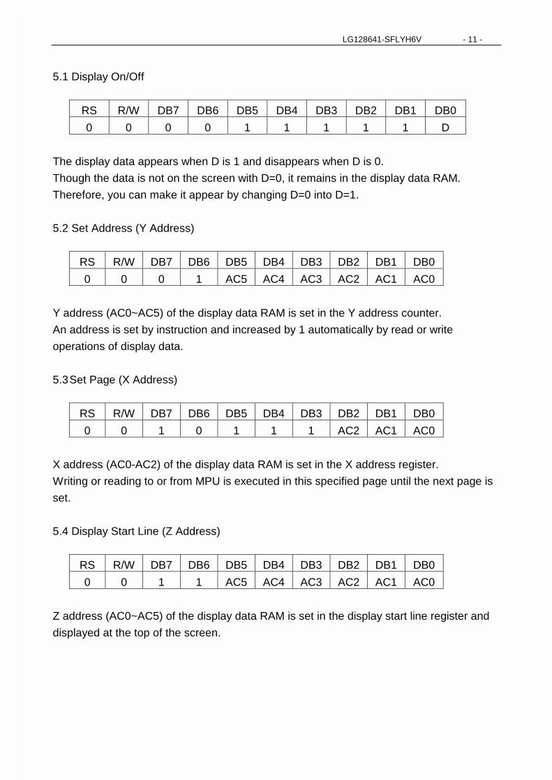
5.1 Display On/Off
RS R/W DB7 DB6 DB5 DB4 DB3 DB2 DB1 DB0
0 0 0 0 1 1 1 1 1 D
The display data appears when D is 1 and disappears when D is 0.
Though the data is not on the screen with D=0, it remains in the display data RAM.
Therefore, you can make it appear by changing D=0 into D=1.
5.2 Set Address (Y Address)
RS R/W DB7 DB6 DB5 DB4 DB3 DB2 DB1 DB0
0 0 0 1 AC5 AC4 AC3 AC2 AC1 AC0
Y address (AC0~AC5) of the display data RAM is set in the Y address counter.
An address is set by instruction and increased by 1 automatically by read or write
operations of display data.
5.3 Set Page (X Address)
RS R/W DB7 DB6 DB5 DB4 DB3 DB2 DB1 DB0
0 0 1 0 1 1 1 AC2 AC1 AC0
X address (AC0-AC2) of the display data RAM is set in the X address register.
Writing or reading to or from MPU is executed in this specified page until the next page is
set.
5.4 Display Start Line (Z Address)
RS R/W DB7 DB6 DB5 DB4 DB3 DB2 DB1 DB0
0 0 1 1 AC5 AC4 AC3 AC2 AC1 AC0
Z address (AC0~AC5) of the display data RAM is set in the display start line register and
displayed at the top of the screen.

LG128641-SFLYH6V - 12 -
5.5 Status Read
RS R/W DB7 DB6 DB5 DB4 DB3 DB2 DB1 DB0
1 0 BUSY 0 ON/OFF RESET 0 0 0 0
• BUSY
When BUSY is 1, the chip is executing internal operation and no instructions are
accepted.
When BUSY is 0, the chip is ready to accept any instructions.
• ON/OFF
When ON/OFF is 1, the display is off.
When ON/OFF is 0, the display is on.
• RESET
When RESET is 1, the system is being initialized.
In this condition, no instructions except status read can be accepted.
When RESET is 0, initializing has finished and the system is in the normal operation
condition.
5.6 Write Display Data
RS R/W DB7 DB6 DB5 DB4 DB3 DB2 DB1 DB0
0 1 D7 D6 D5 D4 D3 D2 D1 D0
Write data (D0~D7) into the display data RAM.
After writing instruction, Y address is increased by 1 automatically.
5.7 Read Display Data
RS R/W DB7 DB6 DB5 DB4 DB3 DB2 DB1 DB0
1 1 D7 D6 D5 D4 D3 D2 D1 D0
Read data (D0~D7) from the display data RAM.
After reading instruction, Y address is increased by 1 automatically.
One time of dummy read must be required after column address setting.

LG128641-SFLYH6V - 13 -
6. DISPLAY DATA RAM ADDRESS MAP
Page Address
Display Data
1st KS0108B 2nd KS0108B Line Address Common
D0 C0 COM1 D1 C1 COM2 D2 C2 COM3 D3 C3 COM4 D4 C4 COM5 D5 C5 COM6 D6 C6 COM7
B8
D7 C7 COM8 D0 C8 COM9 D1 C9 COM10 D2 CA COM11 D3 CB COM12 D4 CC COM13 D5 CD COM14 D6 CE COM15
B9
D7 CF COM16 D0 D0 COM17 D1 D1 COM18 D2 D2 COM19 D3 D3 COM20 D4 D4 COM21 D5 D5 COM22 D6 D6 COM23
BA
D7 D7 COM24 D0 D8 COM25 D1 D9 COM26 D2 DA COM27 D3 DB COM28 D4 DC COM29 D5 DD COM30 D6 DE COM31
BB
D7 DF COM32 D0 E0 COM33 D1 E1 COM34 D2 E2 COM35 D3 E3 COM36 D4 E4 COM37 D5 E5 COM38 D6 E6 COM39
BC
D7 E7 COM40 D0 E8 COM41 D1 E9 COM42 D2 EA COM43 D3 EB COM44 D4 EC COM45 D5 ED COM46 D6 EE COM47
BD
D7 EF COM48 D0 F0 COM49 D1 F1 COM50 D2 F2 COM51 D3 F3 COM52 D4 F4 COM53 D5 F5 COM54 D6 F6 COM55
BE
D7 F7 COM56 D0 F8 COM57 D1 F9 COM58 D2 FA COM59 D3 FB COM60 D4 FC COM61 D5 FD COM62 D6 FE COM63
BF
D7 FF COM64 Column
Address 40 41 42 -- 7D 7E 7F 40 41 42 -- 7D 7E 7F
Segment
SE
G1
SE
G2
SE
G3
--
SE
G62
SE
G63
SE
G64
SE
G65
SE
G66
SE
G67
--
SE
G12
6
SE
G12
7
SE
G12
8

LG128641-SFLYH6V - 14 -
7. CONNECTION WITH 8051 FAMILY MPU
8
b. Application Circuit 2
P3.3
RST
P3.4
P1.0~P1.7
P3.2
P3.1
P3.0
DB0~DB7
/RST
/CS1
/CS2
RS
E
R/W
A3A2A1A0
a. Application Circuit 1
8051
8051
RST
/WR/RD
P2.5~P2.73
P0.0~P0.7
74LS138
Y0
74LS373
8
8KS0108
KS0108
/RST
E
DB0~DB7
/CS2
RSR/W/CS1

LG128641-SFLYH6V - 15 -
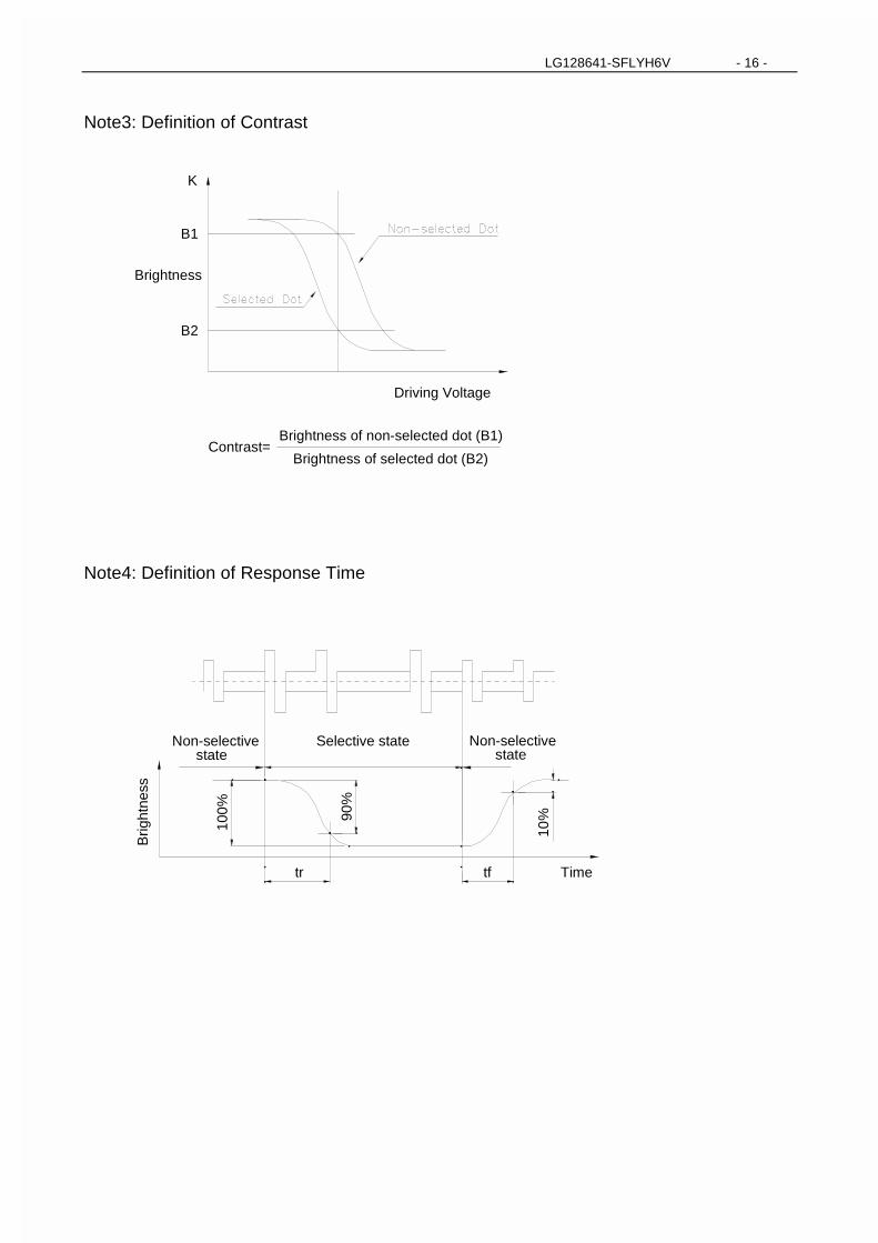
8. ELECTRO OPTICAL CHARACTERISTICS (Ta=25 )
Item Symbol Condition Min. Typ. Max. Unit Note
View Angle 2- 1 K≥2 , θ=0 -- 60 -- Deg Note1, Note2
Contrast K =0 ,θ=0 3 -- -- -- Note3
tr (rise) =0 ,θ=0 -- 250 -- ms Response Time
tf (fall) =0 ,θ=0 -- 250 -- ms Note3
Note1: Definition of Viewing Angle ,
φ1φ2
θ
X X'
Y( =180
φ
θ )
=0θY'( )
=0Z( ) Top
Bottom, φ=+90
, φ =-90
Note2: Definition of viewing Angle Range: 1, 2
φ1Viewing Angle
φ2
2.0
K
LG128641-SFLYH6V - 16 -
Note3: Definition of Contrast
K
B1
B2
Brightness
Driving Voltage
Contrast=Brightness of selected dot (B2)
Brightness of non-selected dot (B1)
Note4: Definition of Response Time
Brig
htne
ss
tr
100% 90
%
10%
tf
Non-selectiveNon-selectivestate state
Selective state
Time

LG128641-SFLYH6V - 17 -
9. DIMENSIONAL OUTLINE

LG128641-SFLYH6V - 18 -
10. LAUREL LCD MODULE NUMBERING SYSTEM
L G 128 64 1 S F L Y H 6 V XX (1) (2) (3) (4) (5) (6) (7) (8) (9) (10) (11) (12) (13)
(1) Brand : Laurel products
(2) Module type
C - Character module
G - Graphic module
(3) Display format
Character module : Number of characters per line, two digits XX
Graphic module : Number of columns, tow or three digits XX or XXX
(4) Display format
Character module : Number of lines, one digits X
Graphic module : Number of rows, two or three digits XX or XXX
(5) Development number : One digit X ( 1~9, A~Z )
(6) LCD mode
T - TN Positive, Gray N - TN Negative, Blue
S - STN Positive, Yellow-green G - STN Positive, Gray
B - STN Negative, Blue F - FSTN Positive, White
K - FSTN Negative, Black
(7) Polarizer mode
R - Reflective F - Transflective M - Transmissive
(8) Backlight type
N - Without backlight L - Array LED D - Edge light LED E - EL C - CCFL
(9) Backlight color
Y - Yellow-green B - Blue W - White G - Green
A - Amber R - Red M - Multi color
(10) Operating temperature range
S - Standard temperature ( 0 ~ +50 oC ) H - Extended Temperature ( -20 ~ +70 oC )
(11) Viewing direction
3 - 3:00 6 – 6:00 9 – 9:00 U – 12:00
(12) DC-DC Converter
N – Without DC-DC converter V – Built in DC-DC converter
(13) Version code
Nil – Standard product 01~ZZ – Version code

LG128641-SFLYH6V - 19 -
11. PRECAUTIONS FOR USE OF LCD MODULE 11.1 Handing Precautions
1) The display panel is made of glass. Do not subject it to a mechanical shock by Dropping it from a high place, etc.
2) If the display panel is damaged and the liquid crystal substance inside it leaks out, be sure not to get any in your mouth. If the substance comes into contact with your Skin or clothes, promptly wash it off using soap and water.
3) Do not apply excessive force on the surface of display or the adjoining areas of LCD module since this may cause the color tone to vary.
4) The polarizer covering the display surface of the LCD module is soft and easily Scratched. Handle this polarizer carefully.
5) If the display surface of LCD module becomes contaminated, blow on the Surface and gently wipe it with a soft dry cloth. If it is heavily contaminated, moisten Cloth with one of the following solvents. Isopropyl alcohol Ethyl alcohol
Solvents other than those mentioned above may damage the polarizer. Especially, do not use the following: Water Ketone Aromatic Solvents
6) When mounting the LCD module make sure that it is free of twisting, warping, and Distortion. Distortion has great influence upon display quality. Also keep the Stiffness enough regarding the outer case.
7) Be sure to avoid any solvent such as flux for soldering never stick to Heat-Seal. Such solvent on Heat-Seal may cause connection problem of heat-Seal and TAB.
8) Do not forcibly pull or bend the TAB I/O terminals. 9) Do not attempt to disassemble or process the LCD module. 10) NC terminal should be open. Do not connect anything. 11) If the logic circuit power is off, do not apply the input signals. 12) To prevent destruction of the elements by static electricity, be careful to maintain
an optimum work environment. Be sure to ground the body when handling the LCD module. Tools required for assembly, such as soldering irons, must be properly grounded. To reduce the amount of static electricity generated, do not conduct assembly
and other work under dry conditions. The LCD module is coated with a film to protect the display surface. Exercise
care when peeling off this protective film since static electricity may be generated.
11.2 Storage Precautions
1) When storing the LCD module, avoid exposure to direct sunlight or to the light of Fluorescent lamps and high temperature/high humidity. Whenever possible, the

LG128641-SFLYH6V - 20 -
LCD module should be stored in the same conditions in which they were shipped from Our company.
2) Exercise care to minimize corrosion of the electrodes. Corrosion of the electrodes is accelerated by water droplets or a current flow in a high humidity environment.
11.3 Design Precautions 1) The absolute maximum ratings represent the rated value beyond which LCD module
can not exceed. When the LCD modules are used in excess of this rated value, their operating characteristics may be adversely affected.
2) To prevent the occurrence of erroneous operation caused by noise, attention must be paid to satisfy VIL, VIH specification values, including taking the precaution of using signal cables that are short.
3) The liquid crystal display exhibits temperature dependency characteristics. Since recognition of the display becomes difficult when the LCD is used outside its designated operating temperature range, be sure to use the LCD within this range. Also, keep in mind that the LCD driving voltage levels necessary for clear displays will vary according to temperature.
4) Sufficiently notice the mutual noise interference occurred by peripheral devices. 5) To cope with EMI, take measures basically on outputting side. 6) If DC is impressed on the liquid crystal display panel, display definition is rapidly
deteriorated by the electrochemical reaction that occurs inside the liquid crystal display panel. To eliminate the opportunity of DC impressing, be sure to maintain the AC characteristics of the input signals sent to the LCD Module.
11.4 Others
1) Liquid crystals solidify under low temperatures (below the storage temperature range) leading to defective orientation or the generation of air bubbles (black or white). Air bubbles may also be generated if the LCD module is subjected to a strong shock at a low temperature.
2) If the LCD modules have been operating for a long time showing the same display patterns, the display patterns may remain on the screen as ghost images and a slight contrast irregularity may also appear. A normal operating status can be regained by suspending use for some time. It should be noted that this phenomenon does not adversely affect performance reliability.
3) To minimize the performance degradation of the LCD modules resulting from destruction caused by static electricity, etc., exercise care to avoid touching the following sections when handling the module: Terminal electrode sections. Part of pattern wiring on TAB, etc.
This datasheet has been downloaded from:
www.DatasheetCatalog.com
Datasheets for electronic components.