krste asanovic [email protected] mit computer science and artificial intelligence laboratory embedded...
Post on 22-Dec-2015
231 views
TRANSCRIPT

Krste Asanovic
[email protected] Computer Science and Artificial Intelligence Laboratory
http://cag.csail.mit.edu/scale
Embedded RAMP Workshop, BWRCAugust 23, 2006
RAMP Design Infrastructure
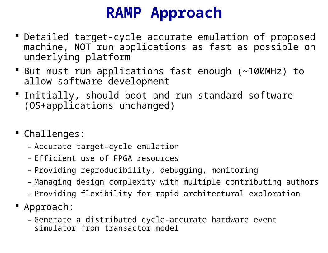
RAMP Approach
Detailed target-cycle accurate emulation of proposed machine, NOT run applications as fast as possible on underlying platform
But must run applications fast enough (~100MHz) to allow software development
Initially, should boot and run standard software (OS+applications unchanged)
Challenges:– Accurate target-cycle emulation
– Efficient use of FPGA resources
– Providing reproducibility, debugging, monitoring
– Managing design complexity with multiple contributing authors
– Providing flexibility for rapid architectural exploration
Approach:– Generate a distributed cycle-accurate hardware event simulator from
transactor model
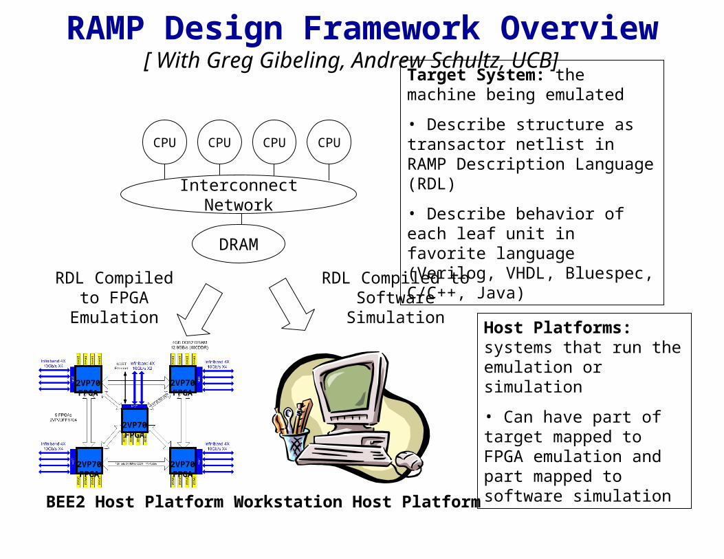
Target System: the machine being emulated
• Describe structure as transactor netlist in RAMP Description Language (RDL)
• Describe behavior of each leaf unit in favorite language (Verilog, VHDL, Bluespec, C/C++, Java)
CPU CPU CPU CPU
Interconnect Network
DRAM
Host Platforms: systems that run the emulation or simulation
• Can have part of target mapped to FPGA emulation and part mapped to software simulation
2VP70FPGA
2VP70FPGA
2VP70FPGA
2VP70FPGA
2VP70FPGA
RDL Compiled to FPGA Emulation
BEE2 Host Platform
RDL Compiled to Software Simulation
Workstation Host Platform
RAMP Design Framework Overview[ With Greg Gibeling, Andrew Schultz, UCB]

UnitsLarge pieces of functionality, >10,000 Gates (e.g. CPU + L1$)Leaf units implemented in a “host” language (e.g., Verilog, C++)
ChannelsUnidirectionalPoint-to-pointFIFO semanticsUnknown latency and buffering (fixed when system instantiated)Implementation generated automatically by RDL compiler
Channel Receiving UnitSending Unit
Port
Port
Units and Channels in RAMP
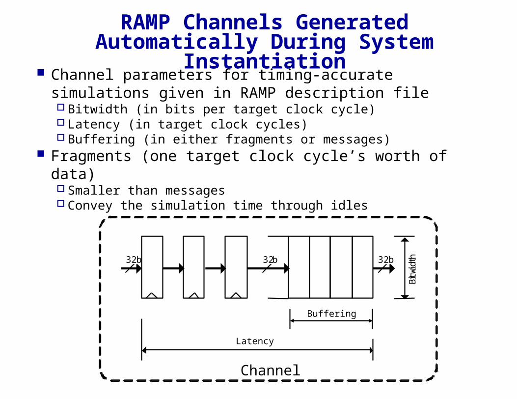
RAMP Channels Generated Automatically During System Instantiation
Channel parameters for timing-accurate simulations given in RAMP description file Bitwidth (in bits per target clock cycle) Latency (in target clock cycles) Buffering (in either fragments or messages)
Fragments (one target clock cycle’s worth of data) Smaller than messages Convey the simulation time through idles
Channel
32b32b 32b
Latency
Buffering
Bitw
idth

Mapping Target Units to Host Platform
Unit
Wrapper
Port B
Port A
Start Done
Port C
Port D
Buffer, Packing &
Timing
Buffer, Packing &
Timing
Timing, Unpacking &
Buffer
Timing, Unpacking &
Buffer
State & Control C ont rol & Stat us
Link A Link C
Outside EdgeInside Edge
Link DLink B
Inside edge, free from host implementation dependencies Needs language-specific version of interface (e.g., Verilog, Bluespec, C++)
Outside edge, implementation dependant Deals with physical links
RDL compiler generates the wrapper and all of the links Allows plugins to extend to new host languages or new link types
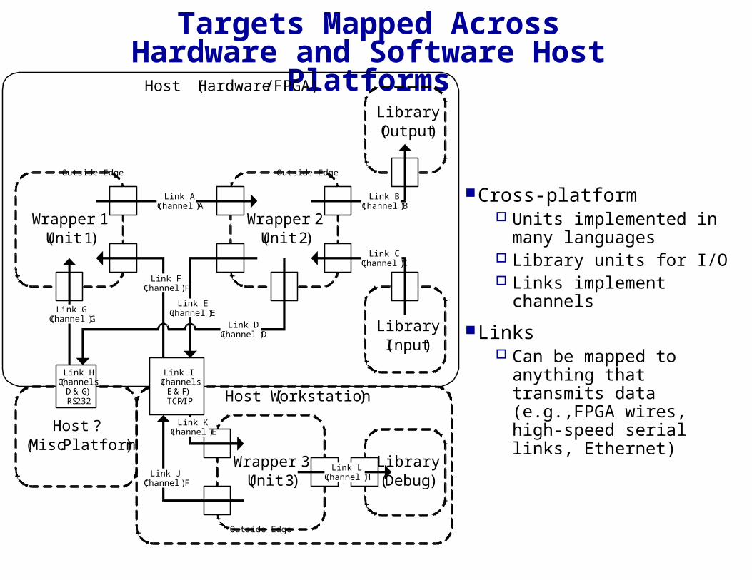
Targets Mapped Across Hardware and Software Host Platforms
Wrapper 1(Unit 1)
Outside Edge
Link F(Channel F)
Link G(Channel G)
Wrapper 2(Unit 2)
Outside Edge
Link D(Channel D)
Link A(Channel A)
Link E(Channel E)
Library(Output)
Link B(Channel B)
Library(Input)
Link C(Channel C)
Host (Hardware/FPGA)
Host ?(Misc. Platform)
Link H(Channels
D & G)RS232 Host (Workstation)
Wrapper 3(Unit 3)
Library(Debug)
Link J(Channel F)
Link K(Channel E)
Outside Edge
Link L(Channel H)
Link I(Channels
E & F)TCP/IP
Cross-platform Units implemented in many
languages Library units for I/O Links implement channels
Links Can be mapped to anything
that transmits data (e.g.,FPGA wires, high-speed serial links, Ethernet)

Virtualization to Improve FPGA Resource Usage
RAMP allows units to run at varying target-host clock ratios to optimize area and overall performance without changing cycle-accurate accounting
Example 1: Multiported register file Example, Sun Niagara has 3 read ports and 2 write ports to 6KB of
register storage If RTL mapped directly, requires 48K flip-flops
Slow cycle time, large area If mapping into block RAMs (one read+one write per cycle), takes 3
host cycles and 3x2KB block RAMs Faster cycle time (~3X) and far less resources
Example 2: Large L2/L3 caches Current FPGAs only have ~1MB of on-chip SRAM Use on-chip SRAM to build cache of active piece of L2/L3 cache,
stall target cycle if access misses and fetch data from off-chip DRAM

Debugging and Monitoring Support
Channel model + target time model supports:
Monitoring All communication over channels can be examined and controlled
Single-stepping by cycle or by transaction Target time can be paused or slowed down
Simulation steering Inject messages into channels
Mixed-mode emulation/simulation Can move some units into software simulation Cross-platform communication hidden by RDL compiler (RDLC)

Related Approaches
FPGA-Based Approaches: Quickturn, Axis, IKOS, Thara:
FPGA- or special-processor based gate-level hardware emulators Slow clock rate (~1MHz vs. RAMP ~100MHz) Limited memory capacity (few GB vs. RAMP 256GB)
RPM at USC in early 1990’s: Up to only 8 processors, only memory controller in configurable logic
Other approaches: Software Simulators Clusters (standard microprocessors) PlanetLab (distributed environment) Wisconsin Wind Tunnel
(used CM-5 to simulate shared memory)All suffer from some combination of: Slowness, inaccuracy, target inflexibility, scalability, unbalanced
computation-communication ratio, ..

DRAMDRAM
DRAM Cntl.DRAM Cntl.
Mem. Sched.Mem. Sched.
Coherence EngineCoherence Engine
RouterRouter
L2$ + L2$ + CoherenceCoherence
CPU + CPU + L1$ + L1$ +
CoherencCoherencee
CPU + CPU + L1$ + L1$ +
CoherencCoherencee
To Other To Other NodesNodes
ISA ISA IndependentIndependent
RAMP White uses scalable directory-based coherence protocol
Multiple different ISAs will eventually be supported
L2$ optional
Target router topology independent of host link topology
Host DRAM used to support host emulation (e.g., L2 cache image) and tracing, as well as target memory
Non-target Non-target accessesaccesses
RAMP White Structure

RAMP for MP-SoC Emulation
Standard TI OMAP 2420 design
CPU& DSP Mapping Optimized with Virtualized RTL
Large on-chip memories virtualized/cached in off-
chip DRAMSelected blocks’ RTL mapped
directly onto FPGA
Off-chip memory held in DRAM, with accurate target timing models
Slower-rate I/O modeled in software on host workstation

Backup

Computing Devices Then
EDSAC, University of Cambridge, UK, 1949

Computing Devices Now
QuickTime™ and aTIFF (Uncompressed) decompressor
are needed to see this picture.
QuickTime™ and aTIFF (Uncompressed) decompressorare needed to see this picture.
QuickTime™ and aTIFF (Uncompressed) decompressor
are needed to see this picture.QuickTime™ and a
TIFF (Uncompressed) decompressorare needed to see this picture.
Robots
SupercomputersAutomobiles
Laptops
Set-top boxes
Games
Smart phones
Servers
Media Players
Sensor Nets
Routers
Cameras

Requirements Converging and Growing Traditional “general-purpose” computing
– Focus on programming effort to implement large and extensible feature set
Traditional embedded computing– Focus on resource constraints (cost, execution time,
power, memory size, …) to implement a fixed function
Current and future computing platforms– Large and growing feature set and resource constraints
(e.g., web browsers on cellphones, power consumption of server farms)
But also, new concerns:– Reliability (hardware and software errors)– Security– Manageability (labor costs)
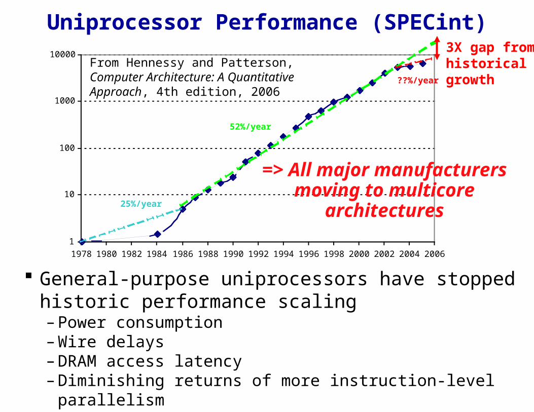
1
10
100
1000
10000
1978 1980 1982 1984 1986 1988 1990 1992 1994 1996 1998 2000 2002 2004 2006
Performance (vs. VAX-11/780)
25%/year
52%/year
??%/year
From Hennessy and Patterson, Computer Architecture: A Quantitative Approach, 4th edition, 2006
3X gap from historical growth
Uniprocessor Performance (SPECint)
=> All major manufacturers moving to multicore
architectures
General-purpose uniprocessors have stopped historic performance scaling– Power consumption– Wire delays– DRAM access latency– Diminishing returns of more instruction-level parallelism
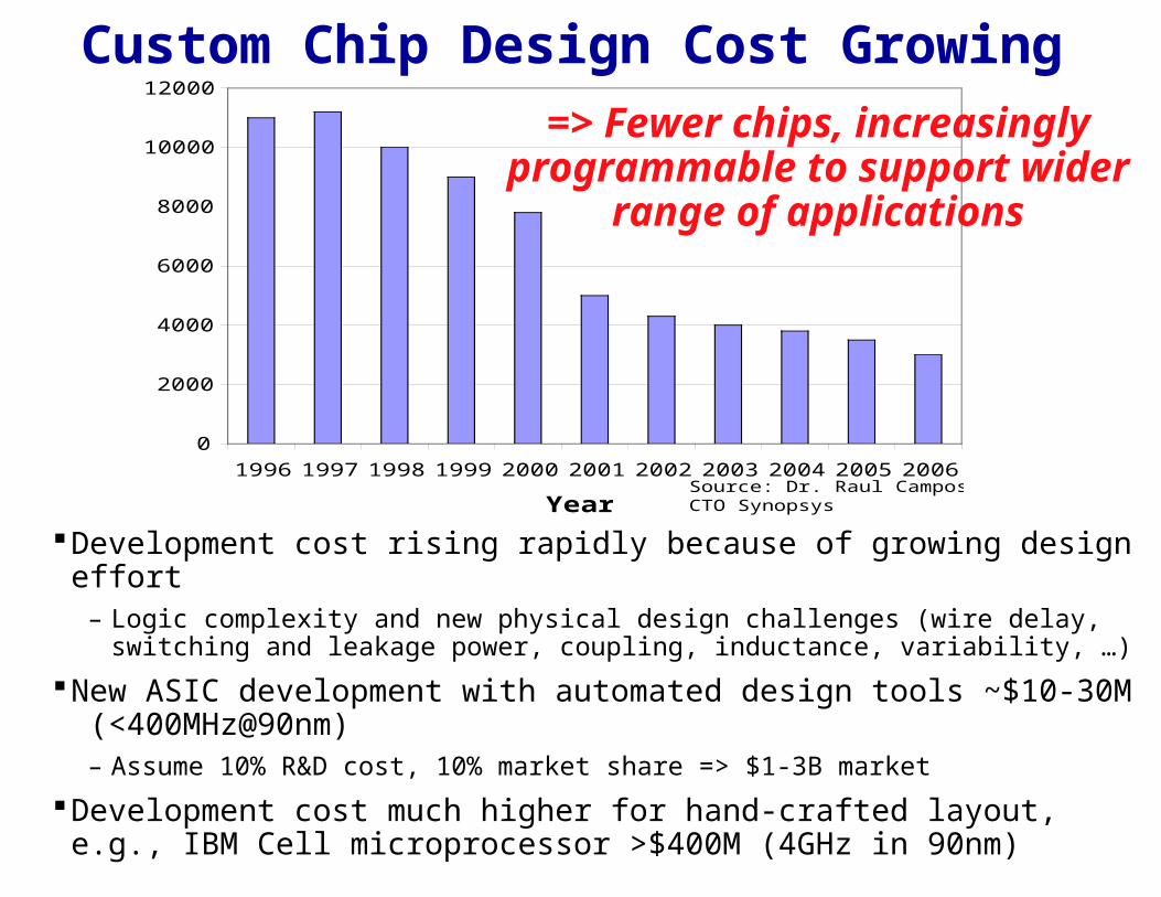
0
2000
4000
6000
8000
10000
12000
1996 1997 1998 1999 2000 2001 2002 2003 2004 2005 2006
Year
No of ASIC design starts
Source: Dr. Raul Camposano, CTO Synopsys
=> Fewer chips, increasingly programmable to support wider
range of applications
Custom Chip Design Cost Growing
Development cost rising rapidly because of growing design effort– Logic complexity and new physical design challenges (wire delay, switching
and leakage power, coupling, inductance, variability, …)
New ASIC development with automated design tools ~$10-30M (<400MHz@90nm)
– Assume 10% R&D cost, 10% market share => $1-3B market
Development cost much higher for hand-crafted layout, e.g., IBM Cell microprocessor >$400M (4GHz in 90nm)

Convergence of PlatformsOnly way to meet system feature set, cost, power, and performance requirements is by programming a processor array– Multiple parallel general-purpose processors (GPPs)– Multiple application-specific processors (ASPs)
“The Processor is the new Transistor” [Rowen]
1000s of processor cores per
die
Intel 4004 (1971): 4-bit processor,
2312 transistors, ~100 KIPS,
10 micron PMOS, 11 mm2 chip
Sun Niagara8 GPP cores (32 threads)
Intel®XScale™
Core32K IC32K DC
MEv210
MEv211
MEv212
MEv215
MEv214
MEv213
Rbuf64 @ 128B
Tbuf64 @ 128B
Hash48/64/128Scratch
16KBQDR
SRAM2
QDRSRAM
1
RDRAM1
RDRAM3
RDRAM2
GASKET
PCI
(64b)66 MHz
IXP2IXP2800800 16b16b
16b16b
1818 18181818 1818
1818 1818 1818
64b64b
SPI4orCSIX
Stripe
E/D Q E/D Q
QDRSRAM
3E/D Q1818 1818
MEv29
MEv216
MEv22
MEv23
MEv24
MEv27
MEv26
MEv25
MEv21
MEv28
CSRs -Fast_wr -UART-Timers -GPIO-BootROM/SlowPort
QDRSRAM
4E/D Q1818 1818
Intel Network Processor1 GPP Core
16 ASPs (128 threads)
IBM Cell1 GPP (2 threads)
8 ASPs
Picochip DSP1 GPP core248 ASPs
Cisco CSR-1188 Tensilica GPPs
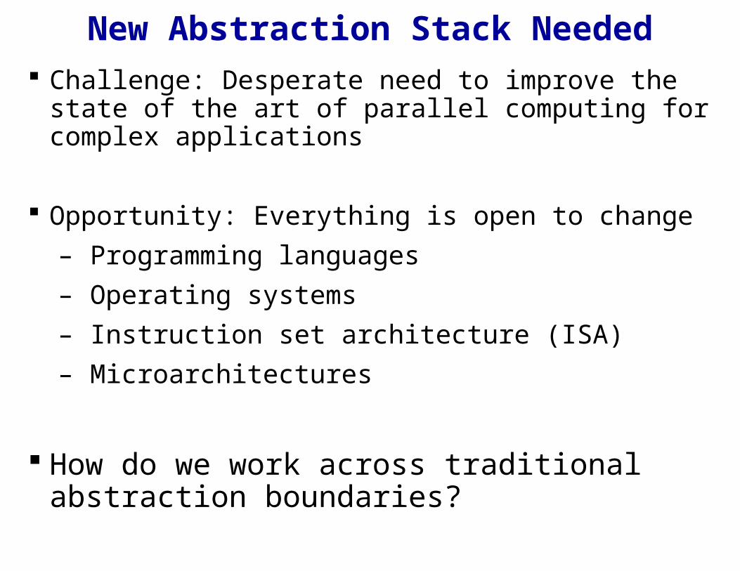
New Abstraction Stack Needed Challenge: Desperate need to improve the state of the art
of parallel computing for complex applications
Opportunity: Everything is open to change
– Programming languages
– Operating systems
– Instruction set architecture (ISA)
– Microarchitectures
How do we work across traditional abstraction boundaries?

Stratification of Research Communities
Algorithm
Gates/Register-Transfer Level (RTL)
Application
Instruction Set Architecture (ISA)
Operating System
Microarchitecture
Devices
Programming Language
Circuits
Hardware community: Software cannot be changed!
Software Community: Hardware cannot be changed!
Problem is not just one of mindset Software developers not interested unless hardware available
– software simulations too slow, ~10-100 kHz for detailed models of one CPU– software simulations not credible
But takes 5 years to complete prototype hardware system!– Then in a few months of software development, all mistakes become clear…

RAMP: Build Research MPP from FPGAs
As 25 CPUs will fit in Field Programmable Gate Array (FPGA), 1000-CPU system from 40 FPGAs?– 16 32-bit simple “soft core” RISC at 150MHz in 2004 (Virtex-II)
– FPGA generations every 1.5 yrs; 2X CPUs, 1.2X clock rate
HW research community does logic design (“gate shareware”) to create out-of-the-box, MPP– E.g., 1000 processor, standard ISA binary-compatible, 64-bit,
cache-coherent supercomputer @ 200 MHz/CPU in 2007
Multi-University Collaboration– RAMPants: Arvind (MIT), Krste Asanovic (MIT), Derek Chiou
(Texas), James Hoe (CMU), Christos Kozyrakis (Stanford), Shih-Lien Lu (Intel), Mark Oskin (Washington), David Patterson (UCB), Jan Rabaey (UCB), and John Wawrzynek (UCB)

RAMP Goals
Provide credible prototypes with sufficient performance to support co-development of software and hardware ideas
Turn-around new hardware ideas in minutes or hours
Support reproducible comparison of ideas across different groups
Architects distribute usable hardware designs by FTP, improve visibility to industry

Board:5 Virtex II FPGAs,
18 banks DDR2-400 memory,
20 10GigE conn.
1.5W / computer,5 cu. in. /computer,$100 / computer
1000 CPUs : 1.5 KW,
$100,000
Box:8 compute modules in 8U rack mount chassis
RAMP-1 Hardware BEE2: Berkeley Emulation Engine 2 By John Wawrzynek and Bob Brodersen with students Chen
Chang and Pierre Droz Completed Dec. 2004 (14x17 inch 22-layer PCB)

Transactors
A transactor (transactional actor) is an abstract unit of computation, which is easy to understand and verify, but which can also be automatically translated into high quality hardware or software implementations

Original Transactor Motivation
Algorithm
Gates/Register-Transfer Level (RTL)
Application
Instruction Set Architecture (ISA)
Operating System
Transactors/Microarchitecture (UTL)
Devices
Programming Language
Circuits
Design chip at microarchitecture level rather than at RTL level Abstract away pipeline depth and communication latencies Separate global communication from local computation Avoid over-specification of behavior, particularly local pipelining &
scheduling Encode “best-practice” in concurrency management
Scale Vector-Thread Processor128 Threads/Core
~1M Gates, 17mm2, 400MHz, 0.18um[IEEE Micro, Top Picks, 2004]

Transactor AnatomyTransactor unit comprises: Architectural state (registers + RAMs) Input queues and output queues connected to other units Transactions (guarded atomic actions on state and queues) Scheduler (selects next ready transaction to run)
Transactions
Scheduler
Input queues
Output queues
Architectural State
Transactor
Advantages Handles non-deterministic inputs Allows concurrent operations on mutable state within unit Natural representation for formal verification

Transactor Networks
Decompose system into network of transactor units
Decoupling global communication and local computation Only communication between units via buffered point-point channels All computation only on local state and channel end-points
Global inter-unit communication via FIFO buffered point-point channels
Short-range local communication within unit
Transactor
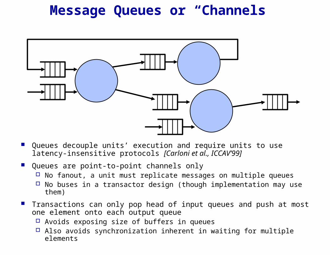
Message Queues or “Channels”
Queues decouple units’ execution and require units to use latency-insensitive protocols [Carloni et al., ICCAV’99]
Queues are point-to-point channels only No fanout, a unit must replicate messages on multiple queues No buses in a transactor design (though implementation may use them)
Transactions can only pop head of input queues and push at most one element onto each output queue Avoids exposing size of buffers in queues Also avoids synchronization inherent in waiting for multiple elements

Transactions Transaction is a guarded atomic action on local state and input
and output queues Guard is a predicate that specifies when transaction can execute
– Predicate is over architectural state and heads of input queues– Implicit conditions on input queues (data available) and output queues
(space available) that transaction accesses Transaction can only pop up to one record from an input queue
and push up to one record on each output queue
transaction
route(input int[32] in,
output int[32] out0,
output int[32] out1)
{
when (routable(in)) {
if (route_func(in) == 0)
out0 = in;
else
out1 = in;
};};
transaction
route_kill(input int[32] in)
{
when (!routable(in)) {
bad_packets++;
};};
Route Stage
in0
in1
out0
out1

Scheduler
Scheduling function decides on transaction priority based on local state and state of input queues– Simplest scheduler picks among ready transactions in a fixed priority order
Transactions may have additional predicates which indicate when they can fire– E.g., implicit condition on all necessary output queues being ready
unitroute_stage(input int[32] in0, // First input channel. input int[32] in1, // Second input channel. output int[32] out0, // First output channel. output int[32] out1) // Second output channel.{ int[32] bad_packets; int[1] last; // Fair scheduler state. schedule { reset { bad_packets = 0; last = 0; };
route_kill(in0);route_kill(in1);
schedule round_robin(last) { (0): route(in0, out0, out1); (1): route(in1, out0, out1);}; }; }
Route Stage
in0
in1
out0
out1
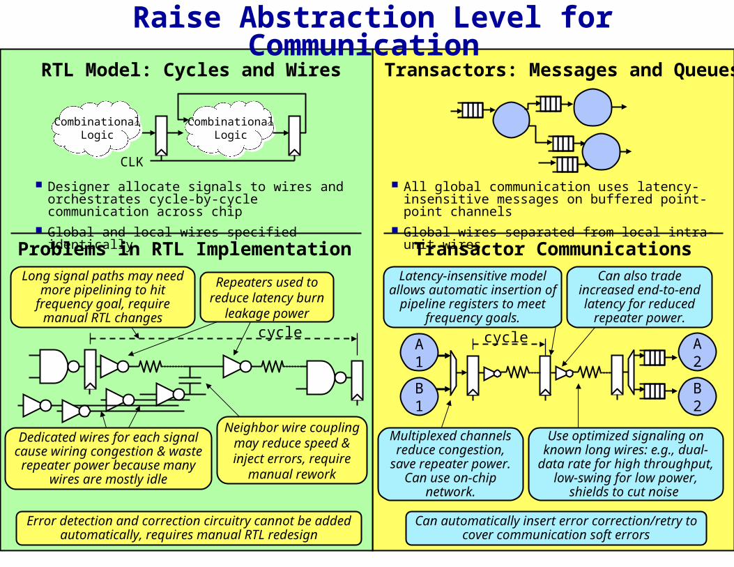
Long signal paths may need more pipelining to hit
frequency goal, require manual RTL changes
Dedicated wires for each signal cause wiring congestion & waste repeater power because many
wires are mostly idle
Neighbor wire coupling may reduce speed & inject errors, require
manual rework
Raise Abstraction Level for Communication RTL Model: Cycles and Wires Transactors: Messages and Queues
Designer allocate signals to wires and orchestrates cycle-by-cycle communication across chip
Global and local wires specified identically
Problems in RTL Implementation
Combinational Logic
CLK
Combinational Logic
Error detection and correction circuitry cannot be added automatically, requires manual RTL redesign
All global communication uses latency-insensitive messages on buffered point-point channels
Global wires separated from local intra-unit wires
Transactor Communications
Use optimized signaling on known long wires: e.g., dual-data rate for high throughput,
low-swing for low power, shields to cut noise
Multiplexed channels reduce congestion,
save repeater power. Can use on-chip
network.
Can also trade increased end-to-end latency for reduced
repeater power.
Can automatically insert error correction/retry to cover communication soft errors
Latency-insensitive model allows automatic insertion of
pipeline registers to meet frequency goals.
Repeaters used to reduce latency burn
leakage power
A1
A2
B1
B2
cycle cycle
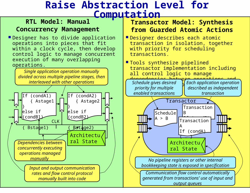
Raise Abstraction Level for Computation
Architectural State
Transaction BIf (condB)----
ScheduleA > B Transaction A
If (condA){ … }
Transactor
CLK
If (condA1) { Astage1 }else if (condB1) { Bstage1}
If (condA2) { Astage2 }else if (condB2) { Bstage2}
Single application operation manually divided across multiple pipeline stages, then
interleaved with other operations
Architectural StateDependencies between
concurrently executing operations managed
manually
RTL Model: Manual Concurrency Management
Designer has to divide application operations into pieces that fit within a clock cycle, then develop control logic to manage concurrent execution of many overlapping operations.
Transactor Model: Synthesis from Guarded Atomic Actions
Designer describes each atomic transaction in isolation, together with priority for scheduling transactions.
Tools synthesize pipelined transactor implementation including all control logic to manage dependencies between operations and flow control of communications.
Each application operation described as independent
transaction
Communication flow control automatically generated from transactions’ use of input and
output queues
Schedule gives desired priority for multiple enabled
transactions
No pipeline registers or other internal bookkeeping state is exposed in specification
Input and output communication rates and flow control protocol
manually built into code

Design Template for Transactor
Scheduler only fires transaction when it can complete without stalls– Avoids driving heavily loaded stall signals
Architectural state (and outputs) only written in one stage of pipeline, use bypass/interlocks to read in earlier stages– Simplifies hazard detection/prevention
Have different transaction types access expensive units (RAM read ports, shifters, multiply units) in same pipeline stage to reduce area
Scheduler
Arch. State 1
Arch. State 2

Transactor VLSI Design Flow
Designer converts specification into
Transactor network
Manual Translation
Transactor
Synthesis
CLK
Automated transactor synthesis produces
optimized gate netlist plus channel portsM
icro
arch
. P
aram
eter
sDesigner specifies desired transactor
microarchitecture and channel bandwidths
Glo
bal
Rou
ting
Channels routed with post-placement
repeater insertion
Place and Local Route
Pla
cem
ent
Dire
ctiv
es
Units placed on die, no global
routing
Designer specifies relative placement of
units on die
Specification

System Design Flow
CPU
DSP
FPGA
ASIC
DRAM
SRAMGeneral-purpose compiler
OS
DSP compilerAssembler
Logic synthesisFPGA tools
Logic synthesisPhysical Design
C ProgramC programAssembly
Verilog/VHDL RTL Code
Verilog/VHDL RTL Code
Generate Software Code
Generate Hardware RTL
Transactor Code

Related Models
CSP/Occam Rendevous communications expose system latencies in design No mutable shared state within a unit
Khan Process Networks (and simpler SDF models) Do not support non-deterministic inputs Sequential execution within unit
Latency-Insensitive Design [Carloni et al.] Channels are similar to transactor channels Units described as stallable RTL
TRS/Bluespec [Arvind & Hoe] Uses guarded atomic actions at RTL level (single cycle
transactions) Microarchitectural state is explicit No unit-level discipline enforced
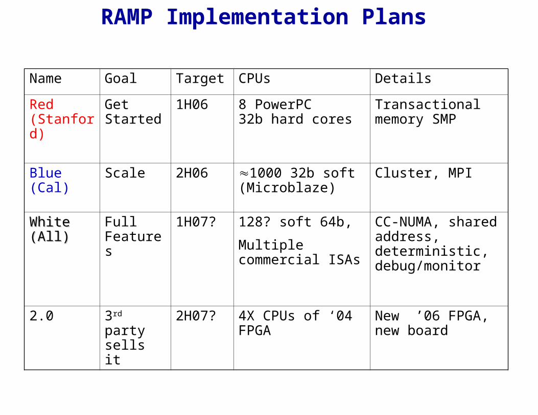
RAMP Implementation Plans
Name Goal Target CPUs Details
Red (Stanford)
Get Started
1H06 8 PowerPC 32b hard cores
Transactional memory SMP
Blue (Cal) Scale 2H06 1000 32b soft (Microblaze)
Cluster, MPI
White (All)White (All) Full Features
1H07? 128? soft 64b,
Multiple commercial ISAs
CC-NUMA, shared address, deterministic, debug/monitor
2.0 3rd party sells it
2H07? 4X CPUs of ‘04 FPGA
New ’06 FPGA, new board

Summary
All computing systems will use many concurrent processors (1,000s of processors/chip) Unlike previously, this is not just a prediction, already happening
We desperately need a new stack of system abstractions to manage complexity of concurrent system design
RAMP project building an emulator “watering hole” to bring everyone together to help make rapid progress architects, OS, programming language, compilers, algorithms, application
developers, …
Transactors provide a unifying model for describing complex concurrent hardware and software systems Complex digital applications The RAMP target hardware itself