krishna saraswat stanford university performance analysis and technology of 3d ics krishna saraswat...
Post on 19-Dec-2015
223 views
TRANSCRIPT

Krishna SaraswatStanford University
Performance Analysis and Technology of 3D ICs
Krishna SaraswatShukri Souri
Kaustav BanerjeePawan Kapur
Department of Electrical EngineeringStanford UniversityStanford, CA 94305
Funding sources: DARPA, MARCO
Krishna SaraswatStanford University
• Why 3-D ICs?
– Limits of Cu/low K technology
• 3D IC performance simulation
• 3-D technologies
– Seeding crystallization of amorphous Si
– Processed wafer bonding
• Thermal simulations
Outline
Krishna SaraswatStanford University
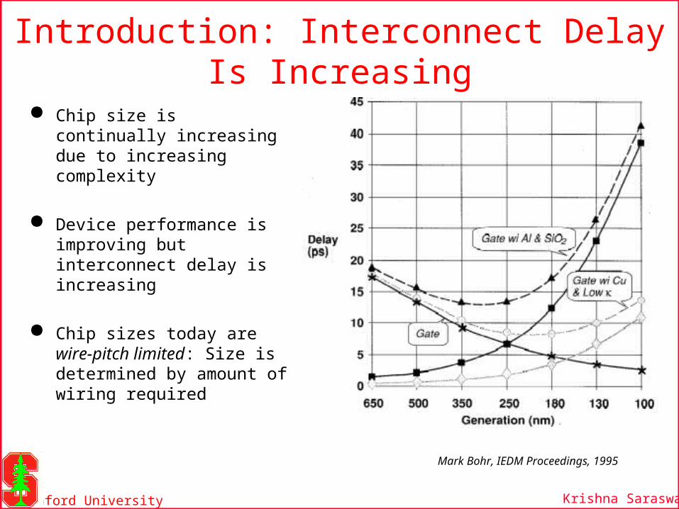
Introduction: Interconnect Delay Is Increasing Chip size is continually
increasing due to increasing complexity
Device performance is improving but interconnect delay is increasing
Chip sizes today are wire-pitch limited: Size is determined by amount of wiring required
Mark Bohr, IEDM Proceedings, 1995

Krishna SaraswatStanford University
Cu Resistivity: Effect of Line Width Scaling•Effect of Cu diffusion Barrier
•Barriers have higher resistivity•Barriers can’t be scaled below a minimum thickness
•Effect of Electron Scattering•Reduced mobility as dimensions decrease
•Effect of Higher Frequencies•Carriers confined to outer skin increasing resistivity
Problem is worse than anticipated in the ITRS 1999 roadmap

Krishna SaraswatStanford University
Cu Resistivity: Barriers Deposition Technology
Atomic Layer Deposition (ALD)
Ionized PVD
Collimated PVD
• 5 nm barrier assumed at the thinnest spot• No scattering assumed, I.e., bulk resistivity
Interconnect dimensions scaled according to ITRS 1999
525250
95 48
280133
ITRS 1999 Line width (nm)GlobelLocal

Krishna SaraswatStanford University
Cu Resistivity: Effect of Electron Scattering
• No barrier assumed• Diffuse electron scattering increases resistivity• Lowering temperature has a big effect
Elastic scattering
Diffuse scattering
ElasticDiffuse, GlobalDiffuse, Local
273 K
373 K
Diffuse, Local
Diffuse, Global
ElasticLower mobility

Krishna SaraswatStanford University
50 100 150 200 250
Technology Generation (nm)
0
10
20
30
p=0.600 p=0.625 p=0.650 p=0.675 p=0.700
As much as 27% of the chip area at 50 nm node is likely to be occupied by repeaters.
Fraction of chip area used by repeaters
Rent’s exponents

Krishna SaraswatStanford University
3D ICs with Multiple Active Si LayersMotivation
• Performance of ICs is limited due to R, L, C of interconnects• Interconnect length and therefore R, L, C can be minimized by stacking active Si layers• Number of horizontal interconnects can be minimized by using vertical interconnects• Disparate technology integration possible, e.g., memory & logic, optical I/O, etc.
Logic
n+/p+
n+/p+ n+/p+
Gate
Gate
T1
T2
M1
M2
M3
M4
n+/p+n+/p+
Gate
Repeatersoptical I/O devices
n+/p+
M’1
M’2
VILIC
Via
MemoryAnalog
Krishna SaraswatStanford University
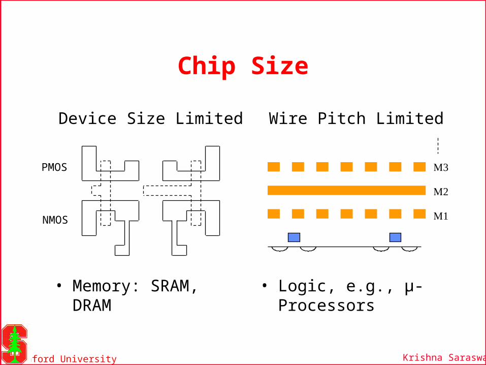
Chip Size
Device Size Limited
• Memory: SRAM, DRAM
Wire Pitch Limited
• Logic, e.g., µ-Processors
PMOS
NMOS

Krishna SaraswatStanford University
Rent’s Rule
T = k N P
T = # of I/O terminalsN = # of gatesk = avg. I/O’s per gateP = Rent’s exponent
N gates

Krishna SaraswatStanford University
Block A with NA gates
Block B
Block C
•Conservation of I/O’sTA + TB + TC = TA-to-B + TA-to-C + TB-to-C +
TABC
• Values of T within a block or collection of blocks are calculated using Rent’s rule, e.g.,
TA = k (NA) P
TABC = k (NA+ NB+ NC) P
• Recursive use of Rent’s rule gives wire-length distribution for the whole chip
TA-to-B = TA + TB -TAB
TB-to-C = TB+ TC -TBC
Determination of Wire-length Distribution
Ref: Davis & Meindl, IEEE TED, March 1998

Krishna SaraswatStanford University
Inter-Layer Connections For 3-D2-Layers
N N/2 N/2
• Fraction of I/O ports T1 and T2 is used for inter-layer connections, Tint
• Assume I/O port conservation:
T = T1 + T2 - Tint
• Use Rent’s Rule: T = kNP to solve for Tint (p assumed constant)
k = Avg. I/O’s per gate N = No. of gates p = Rent’s exponent
T T1 T2

Krishna SaraswatStanford University
Vertical inter-layer connections reduce metal wiring requirement
Single Layer1 2
3 45
2 Layers1 45
3 2
Wire-length Distribution of 3-D IC
Replace horizontal by vertical interconnect
Microprocessor Example from NTRS 50 nm NodeNumber of Gates 180 millionMinimum Feature Size 50 nmNumber of wiring levels, 9Metal Resistivity, Copper 1.673e-6 Ω-cmDielectric Constant, Polymer er = 2.5
1 10 100 1000
1E-4
1E-2
1E0
1E2
1E4
1E6
1E8
Interconnect Length, l (gate pitches)
2D
3D
Local GlobalSemiglobal
LSemi-global
LLocal

Krishna SaraswatStanford University
Chip Area Estimation
Global
Semi-global
Local
A 3-tier wiring network
Achip=A loc+A semi+A glob
#ofmetallayers
• Placement of a wire in a tier is determined by some constraint, e.g., maximum allowed RC delay
• Wiring Area = wire pitch x total lengthAreq = plocLtot_loc + psemiLtot_semi + pglobLtot_glob
= Aloc + Asemi + Aglob
• Ltot calculated from wire-length distribution

Krishna SaraswatStanford University
2 Active Layer Results
• Upper tiers pitches are
reduced for constant chip
frequency, fc
• Less wiring needed
• Almost 50% reduction in
chip area
1 Layer (2-D)2 Layers (3-D)
2-D (1 Layer)7.9 cm 2
3-D (2 Layers)4.0 cm 2
Normalized Semi-global pitch
4
8
12
1 2 3 4
16
20
0

Krishna SaraswatStanford University
3-D Wire-Length DistributionSymmetric Interconnects: Comparable inter- and intra-device layer connectivity
Asymmetric Interconnects:Negligible inter-device layer connectivity
N: Number of logic gates, f.o.: fan-out, k and p: Rent’s parameters, Nz: Number of device layers
More vertical interconnects required
Ref: Rahman & Reif (MIT)

Krishna SaraswatStanford University
More than 2 active layers
Microprocessor Application
PHYSICAL PARAMETER VA LUE
Number of Gates, N 180 million
Rent’s Exponent, p 0.6
Rent’s Coefficient, k 4.0
Minimum Feature Size, F 50nm
Max number of wiring levels, nmax 9
Operating Frequency 3 GHz
Metal Resistivity, Copper 1.673e-6 Ω-cm
Dielectric Constant, Polymer εr = .5Wiri ngEfficiency Factor 0.4
No. of Active Layers
Nor
mal
ized
Int
erco
nnec
t D
elay
1 2 3 4 50.65
0.75
0.85
0.95
1.0

Krishna SaraswatStanford University
Delay of Scaled 2D and 3D ICs • Moving repeaters to upper active
tiers reduces interconnect delay by 9%.
• 3D (2 Si layers) shows significant delay reduction (64%).
• Increasing the number of metal levels in 3D improves interconnect delay by another 40%.
• Increasing the number of Si layers to 5 further improves interconnect delay. 50 100 150 200 250
0.1
1.0
Technology Generation (nm)
Typical gate Delay
0.01
Interconnect Delay
0.001
2D IC with repeaters 3D IC constant metal layers 3D IC metal layers2X3D IC 2X metal layers, 5 Si layers
Interconnect Delay:
Simulations assumed state-of-the-art chip at a technology node with data from NTRS

Krishna SaraswatStanford University
3D Approaches
Epitaxial Lateral Overgrowth (Purdue)Seeding crystallization of -Si
(Stanford)
Wafer Bonding (MIT)
Logic
n+/p+
n+/p+ n+/p+
Gate
Gate
T1
T2
M1
M2
M3
M4
n+/p+n+/p+
Gate
Repeaters or optical I/O devices
n+/p+
M’1
M’2
VILIC
Via
Memory orAnalog

Krishna SaraswatStanford University
Substrate
ChannelDrain
Gate Oxide
Gate
Source
Grains inChannel
Smooth Interface(Crystallized a-Si)
Deposited GateDielectric
Crystallized usinglasers , RTA, or long
furnace anneals
Statistical Variations in Poly-TFT PropertiesConventional Poly-TFT
• As channel length grain size, statistical variation increases
• Elimination of grain boundaries should reduce this variation
0%
20%
40%
60%
80%
100%
0 20 40 60 80 100 120
Mobility (cm
2
/V·s)
L = 1 µm
20 µm
2 µmMobility
Grain size 0.3-0.5 µm
1.E-121.E-111.E-101.E-091.E-081.E-071.E-061.E-051.E-041.E-03
-2 -1 0 1 2 3 4VGS (V)
ID (A/μ )m
VDS = .0VW/L = 0.μm/0.μm
0, Ge-seeded , unseeded , unseeded>4, unseeded
Number of Grain BoundariesNumber of Grain Boundaries0, Ge seeded1, unseeded2, unseeded3, unseeded
Effect of Grain Boundaries
Krishna SaraswatStanford University
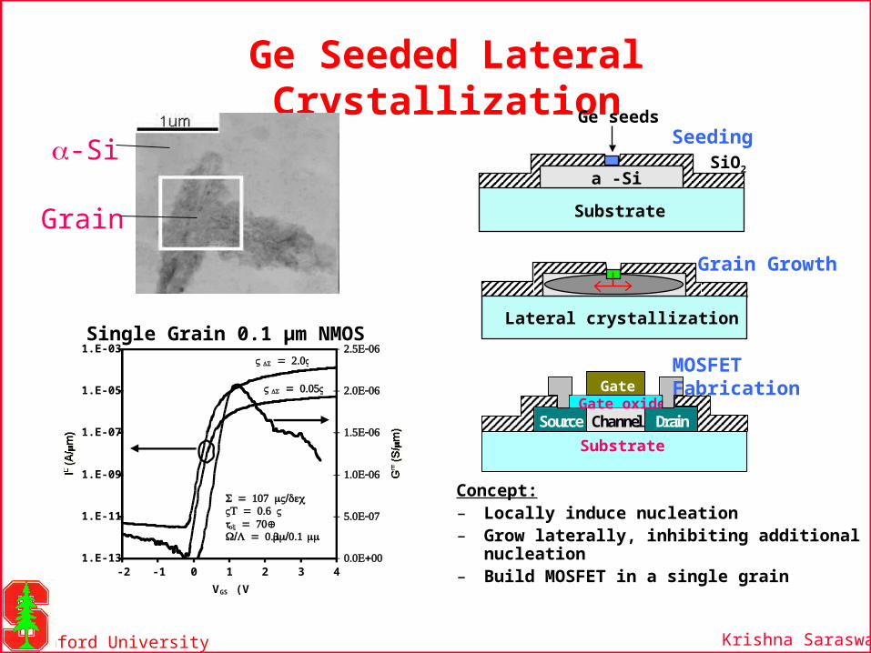
Ge Seeded Lateral Crystallization
Concept:– Locally induce nucleation– Grow laterally, inhibiting additional nucleation– Build MOSFET in a single grain
Grain
-SiGe seeds
Lateral crystallization
a -Si
Substrate
SiO2
Seeding
Grain Growth
Substrate
ChannelSource DrainGate oxide
GateMOSFET Fabrication
1.E-13
1.E-11
1.E-09
1.E-07
1.E-05
1.E-03
-2 -1 0 1 2 3 4
VGS (V)
ID (A/
μ )m
0.0 +00E
5.0 -07E
.0 -06E
.5 -06E
.0 -06E
.5 -06E
Gm ( /Sμ )m
VDS = .0V
VDS = 0.05V
= 07 /S mV dec = 0.6 VT V
tox = 70Å/ = 0.W L μ /0.m μm
Single Grain 0.1 µm NMOS

Krishna SaraswatStanford University
0
50
100
150
200
250
300
0 2 4 6 8 10 12 14 16 18 20
Drawn Channel Length, L (um)
Control
Seed
1.E-121.E-111.E-101.E-091.E-081.E-071.E-061.E-051.E-041.E-03
-2 -1 0 1 2 3 4VGS (V)
ID (A/μ )m
VDS = .0VW/L = 0.μm/0.μm
0, Ge-seeded , unseeded , unseeded>4, unseeded
Number of Grain BoundariesNumber of Grain Boundaries0, Ge seeded1, unseeded2, unseeded3, unseeded
Single Grain Transistors in Ge Induced Crystallized Si
ID-VG of 0.1 µm NMOS Mobility
SGT

Krishna SaraswatStanford University
Ni Seeded Lateral Crystallization
• Initially transistor fabricated in -Si• Ni seeding for simultaneous crystallization and dopant activation • Low thermal budget (≤ 450°C) •Devices could be fabricated on top of a metal line
-SiCrystallized Si
Ni seedSiGe gate
substrate
SiO2
NMOS
Tmax = 450ºC

Krishna SaraswatStanford University
• Energy is dissipated during transistor operation• Heat is conducted through the low thermal conductivity dielectric,
Silicon substrate and packaging to heat sink• 1-D model assumed to calculate die temperature
SilicontSi
Passivation
TDie
Package
Tpkg
Heat SinkTsink
Heat FlowtPkg
GateVDie
V sink
RSi
I
R Pkg
V Package
a ) b)
40
60
80
100
120
140
160
180
0 50 100 150 200 250 300
Technology Node [nm]
Maximum Power Dissipation [W]
2
3
4
5
6
7
8
9
10
Chip Area [cm
2 ]
2-D Circuits
Power Dissipation for 2D
Thermal Behavior in 3D ICs

Krishna SaraswatStanford University
3D Examples for Thermal Study
• Case A: Heat dissipation is confined to one surface
Bulk Si
n+
p+ p+
Gate
Gate
T1
T2
M1
M2
M3
M4
n+
M’1
M’2
• Case B: Heat dissipation possible from 2 surfaces.
M3
M4
M5
M6
Bulk Si
n+
Gate
T1n+
M’1
M’2
Bulk Si
T2Gate
n+n+

Krishna SaraswatStanford University
010020030040050060070080090010001100120013001400
0 0.5 1 1.5 2 2.5 3 3.5 4Normalized Thermal Resistance, Rn [0C/(Wcm-2)]
Die Temperature [
0C] 3-D: Case-a3-D: Case-b
2-D
Value of Rn with current heat-sinking technology for (2-D) 250 nm nodeValue of Rn for a high-performance heat sinking technology [65]
Attainable die temperatures for 2-D and 3-D ICs at the NTRS based 50 nm node using advanced heat-sinking technologies that would reduce the normalized thermal resistance, R
Die Temperature Simulation

Krishna SaraswatStanford University
3D ICs: Implications for Circuit Design • Critical Path Layout: By vertical stacking, the distance between logic blocks on
the critical path can be reduced to improve circuit performance.
• Integration of disparate technologies is easier
• Microprocessor Design: on-chip caches on the second active layer will reduce distance from the logic and computational blocks.
• RF and Mixed Signal ICs: Substrate isolation between the digital and RF/analog components can be improved by dividing them among separate active layers - ideal for system on a chip design.
• Optical I/O can be integrated in the top layer
• Repeaters: Chip area can be saved by placing repeaters (~ 10,000 for high performance circuits) on the higher active layers.
• Physical Design and Synthesis: Due to a non-planar target graph (upon which the circuit graph is embedded), placement and routing algorithms, and hence synthesis algorithms and architectural choices, need to be suitably modified.

Krishna SaraswatStanford University
• Cu/low k will not solve the problems of interconnects.
• Modeling of interconnect delay shows significant improvement by transitioning from 2-D to 3-D ICs.
• Seeding and lateral crystallization of amorphous Si is a promising technique to implement 3-D ICs.
• Thermal dissipation in 3-D ICs may require innovative packaging solutions.
Summary