key or ganisation for research in integrated circuits in ... · korrigan esa – mod workshop on...
TRANSCRIPT
KORRIGAN
ESA – MOD WORKSHOP ON GaN MICROWAVE COMPONENT TECHNO LOGIES _ Ulm _ March 2009
Overview of the KORRIGAN project
Key Organisation for Research in Integrated Circuits in GaN Technology
Authors: Philippe Duême ( SLIE), Thales Airborne Systems _ France,Andrew Phillips, WP leader ( System Impact ), Phconsult for Selex-Galileo _ UK Trevor Martin / David Wallis, SP leader ( Material ), QinetiQ _ UKAntonio Cetronio, SP leader ( Processing ), Selex-SI _ ItalyEnrico Zanoni, SP leader ( Reliability ), University Padova _ ItalySylvain Delage, SP leader ( Thermal Management ), ATL3-5Lab _ FranceJohan Carlert, SP leader ( Demonstrators ), Saab MS _ SwedenYves Mancuso, Thales Airborne Systems _ FranceIain Davies, Selex Galileo _ UKNiklas Henelius, Norstel, _ SwedenMarc Van Heijningen, TNO _ The NetherlandsTibault Reveyrand, XLIM _ France
KORRIGAN
ESA – MOD WORKSHOP ON GaN MICROWAVE COMPONENT TECHNO LOGIES _ Ulm _ March 2009
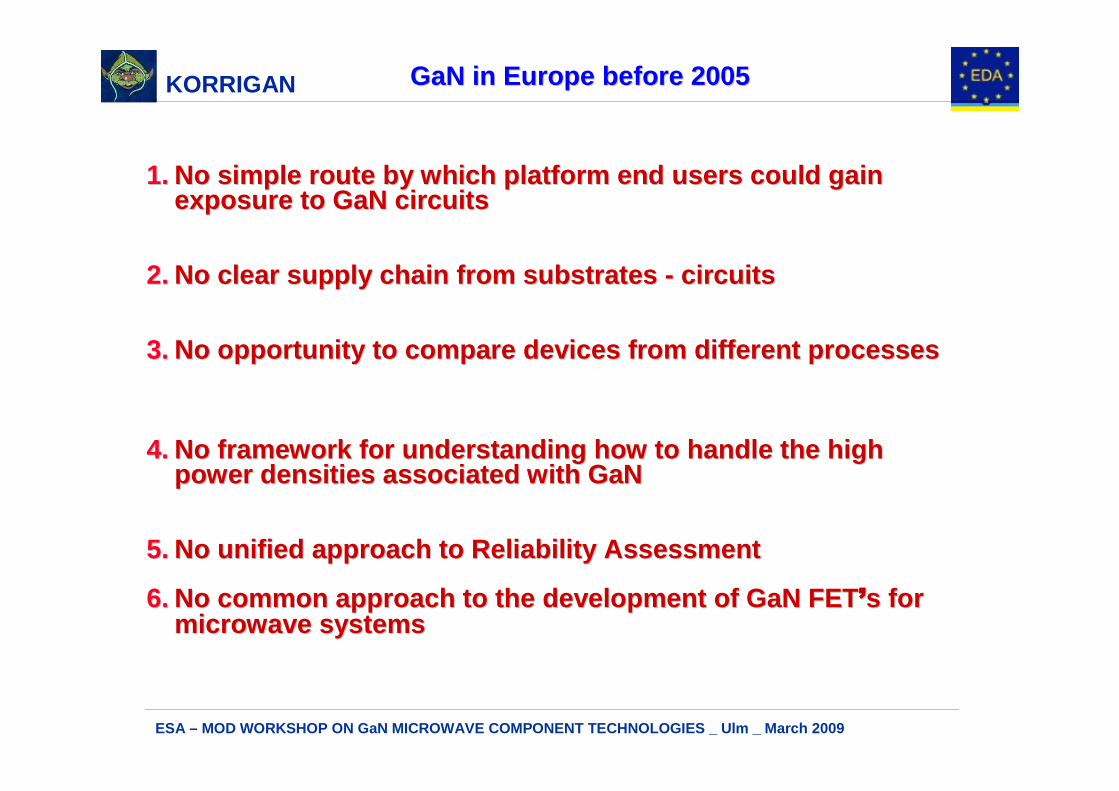
GaN in Europe before 2005GaN in Europe before 2005
1.1. No simple route by which platform end users could gai n No simple route by which platform end users could gai n exposure to GaN circuitsexposure to GaN circuits
2.2. No clear supply chain from substrates No clear supply chain from substrates -- circuitscircuits
3.3. No opportunity to compare devices from different proces sesNo opportunity to compare devices from different proces ses
4.4. No framework for understanding how to handle the hig h No framework for understanding how to handle the hig h power densities associated with GaNpower densities associated with GaN
5.5. No unified approach to Reliability AssessmentNo unified approach to Reliability Assessment
6.6. No common approach to the development of GaN No common approach to the development of GaN FETFET’’’’’’’’ss for for microwave systemsmicrowave systems
KORRIGAN
ESA – MOD WORKSHOP ON GaN MICROWAVE COMPONENT TECHNO LOGIES _ Ulm _ March 2009
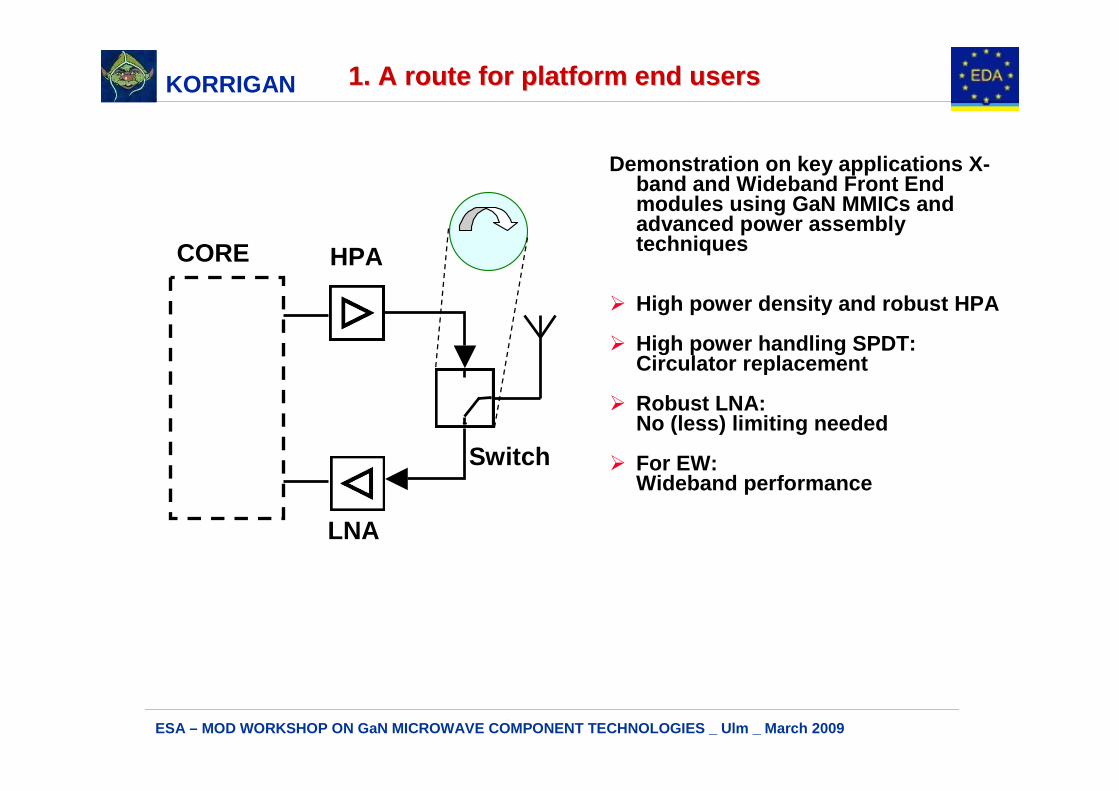
1. A route for platform end users1. A route for platform end users
Demonstration on key applications X-band and Wideband Front End modules using GaN MMICs and advanced power assembly techniques
� High power density and robust HPA
� High power handling SPDT:Circulator replacement
� Robust LNA: No (less) limiting needed
� For EW:Wideband performance
CORE HPA
LNA
Switch
KORRIGAN
ESA – MOD WORKSHOP ON GaN MICROWAVE COMPONENT TECHNO LOGIES _ Ulm _ March 2009
MMIC DemonstratorsMMIC Demonstrators
� Building blocks for radar and EW front-ends
� S-Band designs (3 GHz)� Power Bars for Hybrid HPAs
� X-Band Designs (8.5 - 10.5 GHz)� HPA MMICs� LNA MMICs� Switch MMICs
� Wide band designs� HPA MMICs (2-6 and 6-18 GHz)� LNA MMICs (2-18 GHz)� Switch MMICs (2-18 GHz)
� A total of 29 circuits demonstrators and 6 modules developed, more than in any programme world wide
� Presentation on Monday afternoon:” KORRIGAN MMIC Demonstrators
Designs and Results”by Marc van Heijningen, TNO
KORRIGAN
ESA – MOD WORKSHOP ON GaN MICROWAVE COMPONENT TECHNO LOGIES _ Ulm _ March 2009
2. A supply chain from substrates to circuits2. A supply chain from substrates to circuits
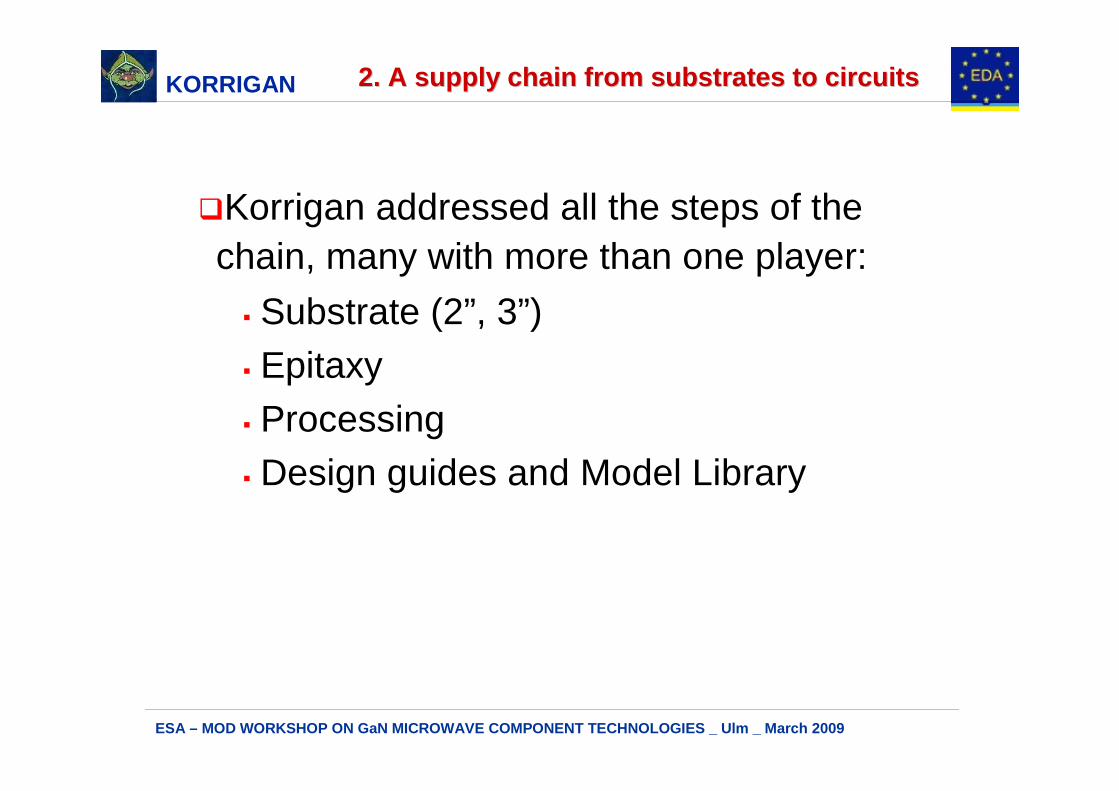
�Korrigan addressed all the steps of the chain, many with more than one player:
� Substrate (2”, 3”)� Epitaxy
� Processing� Design guides and Model Library

KORRIGAN
ESA – MOD WORKSHOP ON GaN MICROWAVE COMPONENT TECHNO LOGIES _ Ulm _ March 2009
SiC semiSiC semi --insulating substratesinsulating substrates
� Norstel AB established in 2005 to industrialise Okmetic/LiU SiC crystal growth
� Significant investements in SiC technology initiated in 2005, partly motivated by the Korrigan requirements
� New custom-built facility commissioned in Norrköping, Sweden
� New furnaces designed for 3” material and prepared for further diameter expansion
� Complete wafering line� Extensive set of characterisation tools
� Regular deliveries of 2” SiC substrates from Norstel to the Korrigan team showing progressive improvement
� Polytype inclusions virtually eliminated� Micropipe density < 2 cm-2 demonstrated� Improved crystalline quality as shown by reduced contrast in crossed polariser images� Device level feedback so far indicates performance comparable to Cree substrates
� 3” substrates sampled
� Strategic collaboration Norstel / AIST (Japan) esta blished (2007) for large-diameter high-quality SiC substrate development and manufacturing
� Long-term effort with first results expected in 2009
KORRIGAN
ESA – MOD WORKSHOP ON GaN MICROWAVE COMPONENT TECHNO LOGIES _ Ulm _ March 2009
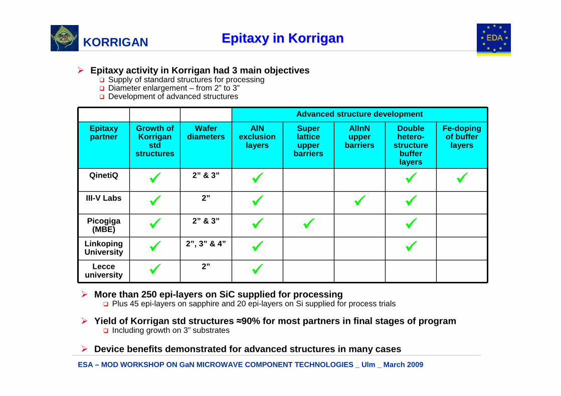
EpitaxyEpitaxy in Korriganin Korrigan
� Epitaxy activity in Korrigan had 3 main objectives � Supply of standard structures for processing� Diameter enlargement – from 2” to 3”� Development of advanced structures
Advanced structure development
Epitaxypartner
Growth of Korrigan
std structures
Wafer diameters
AlNexclusion
layers
Super lattice upper
barriers
AlInNupper
barriers
Double hetero-
structure buffer layers
Fe-doping of buffer
layers
QinetiQ����
2” & 3”���� ���� ����
III-V Labs����
2”���� ���� ����
Picogiga(MBE) ����
2” & 3”���� ���� ����
LinkopingUniversity ����
2”, 3” & 4”���� ����
Lecceuniversity ����
2”����
� More than 250 epi-layers on SiC supplied for process ing� Plus 45 epi-layers on sapphire and 20 epi-layers on Si supplied for process trials
� Yield of Korrigan std structures ≈90% for most partners in final stages of program� Including growth on 3” substrates
� Device benefits demonstrated for advanced structure s in many cases
KORRIGAN
ESA – MOD WORKSHOP ON GaN MICROWAVE COMPONENT TECHNO LOGIES _ Ulm _ March 2009
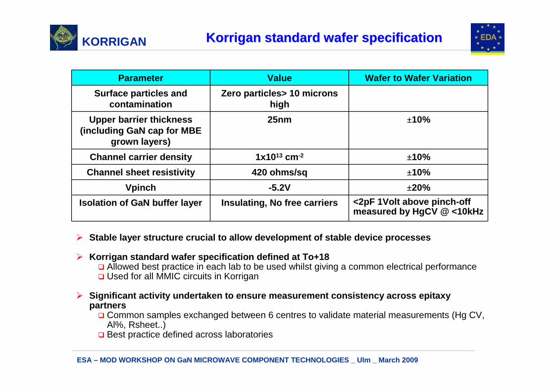
Korrigan standard wafer specificationKorrigan standard wafer specification
� Stable layer structure crucial to allow development of stable device processes
� Korrigan standard wafer specification defined at To +18� Allowed best practice in each lab to be used whilst giving a common electrical performance� Used for all MMIC circuits in Korrigan
� Significant activity undertaken to ensure measureme nt consistency across epitaxypartners
� Common samples exchanged between 6 centres to validate material measurements (Hg CV, Al%, Rsheet..)
� Best practice defined across laboratories
Parameter Value Wafer to Wafer Variation
Surface particles and contamination
Zero particles> 10 microns high
Upper barrier thickness (including GaN cap for MBE
grown layers)
25nm ±10%
Channel carrier density 1x10 13 cm -2 ±10%
Channel sheet resistivity 420 ohms/sq ±10%
Vpinch -5.2V ±20%
Isolation of GaN buffer layer Insulating, No free ca rriers <2pF 1Volt above pinch-off measured by HgCV @ <10kHz
KORRIGAN
ESA – MOD WORKSHOP ON GaN MICROWAVE COMPONENT TECHNO LOGIES _ Ulm _ March 2009
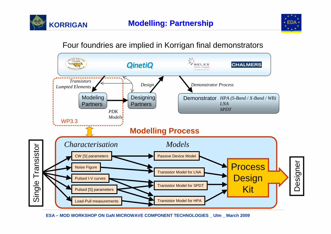
Four foundries are implied in Korrigan final demonstrators
ModelingPartners
DesigningPartners
Demonstrator HPA (S-Band / X-Band / WB)LNASPDT
TransistorsLumpted Elements
PDKModels
Design Demonstrator Process
WP3.3
Modelling Process
CW [S] parameters
Load-Pull measurements
Pulsed I-V curves
Noise Figure
Passive Device Model
Transistor Model for LNA
Transistor Model for SPDT
Transistor Model for HPA
Pulsed [S] parameters
ProcessDesign
Kit
Sin
gle
Tra
nsis
tor
Des
igne
r
Characterisation Models
Modelling: PartnershipModelling: Partnership
KORRIGAN
ESA – MOD WORKSHOP ON GaN MICROWAVE COMPONENT TECHNO LOGIES _ Ulm _ March 2009
Measurements @ power optimal load impedance
10 20 30 40 50 600 70
0.2
0.4
0.6
0.0
0.8
indep(cycle)
cycl
e
X1.Vd_int
rese
au_I
V_s
dd..I
ds_i
nt.i
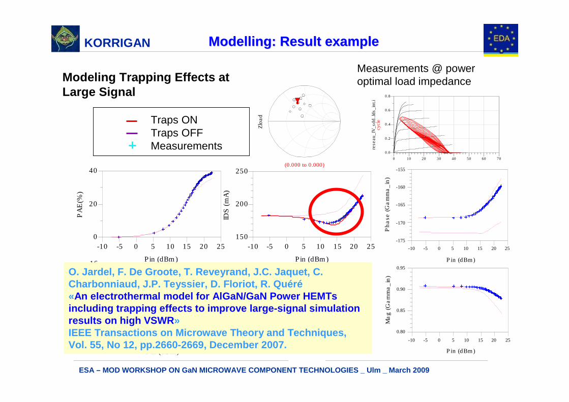
Modeling Trapping Effects at Large Signal
-5 0 5 10 15 20-10 25
0.85
0.90
0.80
0.95
P in (dBm )
Ma
g (
Ga
mm
a_
in)
-5 0 5 10 15 20-10 25
-170
-165
-160
-175
-155
P in (dBm )
Ph
ase
(G
am
ma
_in
)
-5 0 5 10 15 20-10 25
20
0
40
Pin (dBm )
PA
E(%
)
-5 0 5 10 15 20-10 25
200
150
250
Pin (dBm )
IDS
(m
A)
0.0
2
0.0
4
0.0
6
0.0
8
0.1
0
0.1
2
0.1
4
0.1
6
0.1
8
0.0
0
0.2
0
1
2
0
3
Pin (W)
Po
ut (
W)
-5 0 5 10 15 20-10 25
12
14
10
16
Pin (dBm )
Ga
in(d
B)
Loadindep(Load)=GammaLoadpoint=0.549 / 110.520impedance = 20.740 + j30.480
0
(0.000 to 0.000)
Zlo
ad
Load
Loadindep(Load)=GammaLoadpoint=0.549 / 110.520impedance = 20.740 + j30.480
0
Modelling: Result exampleModelling: Result example
O. Jardel, F. De Groote, T. Reveyrand, J.C. Jaquet, C. Charbonniaud, J.P. Teyssier, D. Floriot, R. Quéré«An electrothermal model for AlGaN/GaN Power HEMTs including trapping effects to improve large-signal si mulation results on high VSWR »IEEE Transactions on Microwave Theory and Techniques , Vol. 55, No 12, pp.2660-2669, December 2007.
Traps ONTraps OFFMeasurements
KORRIGAN
ESA – MOD WORKSHOP ON GaN MICROWAVE COMPONENT TECHNO LOGIES _ Ulm _ March 2009
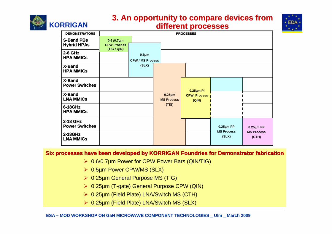
3. An opportunity to compare devices from 3. An opportunity to compare devices from different processesdifferent processes
Six processes have been developed by KORRIGAN Found ries for DemoSix processes have been developed by KORRIGAN Found ries for Demo nstrator fabricationnstrator fabrication
� 0.6/0.7µm Power for CPW Power Bars (QIN/TIG)
� 0.5µm Power CPW/MS (SLX)
� 0.25µm General Purpose MS (TIG)
� 0.25µm (T-gate) General Purpose CPW (QIN)
� 0.25µm (Field Plate) LNA/Switch MS (CTH)
� 0.25µm (Field Plate) LNA/Switch MS (SLX)
X-Band LNA MMICs
2-18GHzLNA MMICs
2-18 GHzPower Switches
6-18GHz HPA MMICs
X-Band Power Switches
X-Band HPA MMICs
2-6 GHz HPA MMICs
S-Band PBsHybrid HPAs
PROCESSESDEMONSTRATORS
X-Band LNA MMICs
2-18GHzLNA MMICs
2-18 GHzPower Switches
6-18GHz HPA MMICs
X-Band Power Switches
X-Band HPA MMICs
2-6 GHz HPA MMICs
S-Band PBsHybrid HPAs
PROCESSESDEMONSTRATORS
0.6 /0.7µµµµmCPW Process
(TIG / QIN)
0.6 /0.7µµµµmCPW Process
(TIG / QIN)
0.5µµµµm
CPW / MS Process
(SLX)
0.5µµµµm
CPW / MS Process
(SLX)
0.25µµµµmMS Process
(TIG)
0.25µµµµmMS Process
(TIG)
0.25µµµµm FPMS Process
(CTH)
0.25µµµµm FPMS Process
(CTH)
0.25µµµµm PiCPW Process
(QIN)
0.25µµµµm PiCPW Process
(QIN)
0.25µµµµm FPMS Process
(SLX)
0.25µµµµm FPMS Process
(SLX)
KORRIGAN
ESA – MOD WORKSHOP ON GaN MICROWAVE COMPONENT TECHNO LOGIES _ Ulm _ March 2009
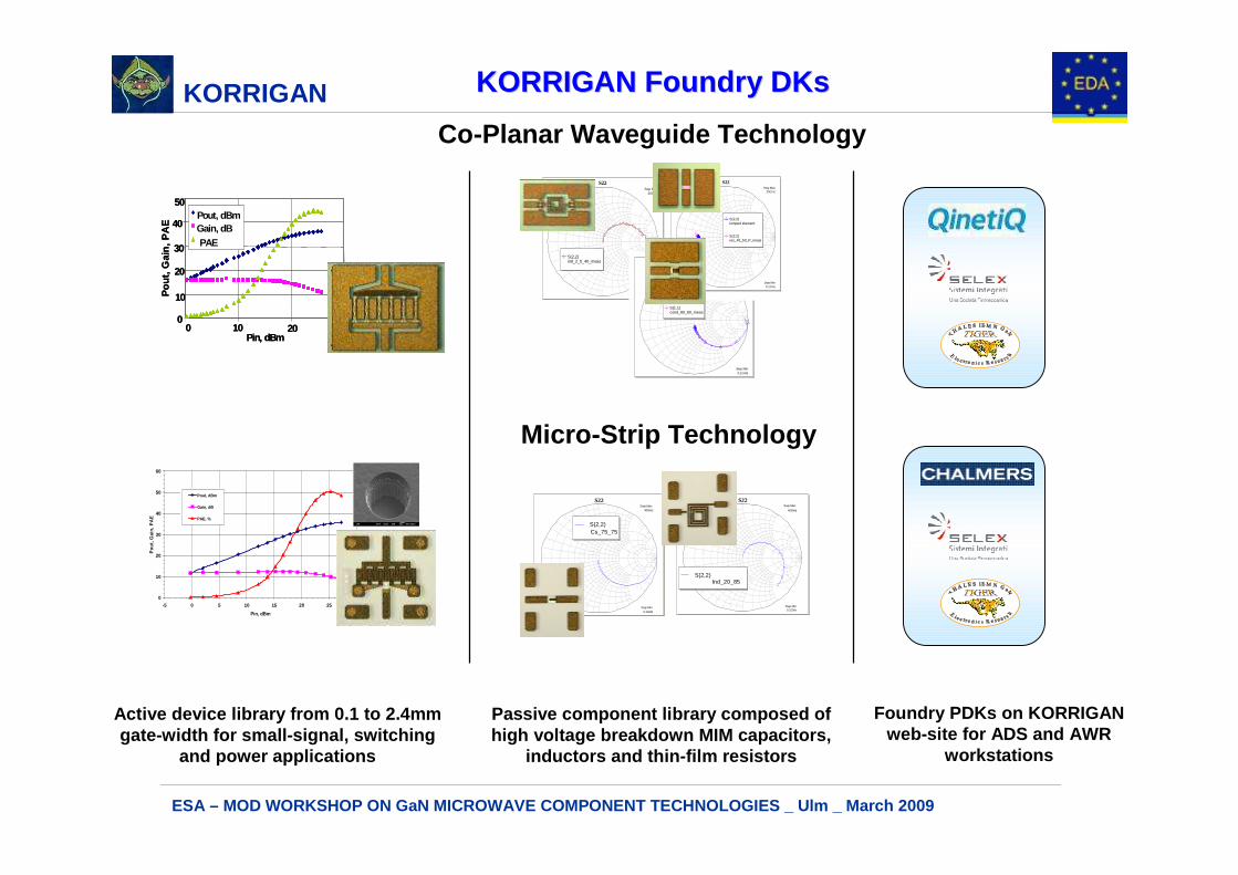
Co-Planar Waveguide Technology
0
10
20
30
40
50
0 10 20 30Pin, dBm
Pou
t, G
ain,
PA
E
Pout, dBmGain, dBPAE
0
10
20
30
40
50
0 10 20 30Pin, dBm
Pou
t, G
ain,
PA
E
Pout, dBmGain, dBPAE
KORRIGAN Foundry KORRIGAN Foundry DKsDKs
0 1.0
1.0
-1.0
10.0
10.0
-10.0
5.0
5.0
-5.0
2.0
2.0
-2.0
3.0
3.0
-3.0
4.0
4.0
-4.0
0.2
0.2
-0.2
0.4
0.4
-0.4
0.6
0.6
-0.6
0.8
0.8
-0.8
S22Swp Max
20GHz
Swp Min0.1GHz
S(2,2)ind_2_5_40_meas
0 1.0
1.0
-1.0
10.0
10.0
-10.0
5.0
5.0
-5.0
2.0
2.0
-2.0
3.0
3.0
-3.0
4.0
4.0
-4.0
0.2
0.2
-0.2
0.4
0.4
-0.4
0.6
0.6
-0.6
0.8
0.8
-0.8
S11Swp Max
20GHz
Swp Min0.1GHz
S(1,1)lumped element
S(1,1)cond_60_60_meas
0 1.0
1.0
-1.0
10.0
10.0
-10.0
5.0
5.0
-5.0
2.0
2.0
-2.0
3.0
3.0
-3.0
4.0
4.0
-4.0
0.2
0.2
-0.2
0.4
0.4
-0.4
0.6
0.6
-0.6
0.8
0.8
-0.8
S22Swp Max
20GHz
Swp Min0.1GHz
S(2,2)lumped element
S(2,2)res_40_50_P_meas0 1
.0
1.0
-1.0
10.0
10.0
-10.0
5.0
5.0
-5.0
2.0
2.0
-2.0
3.0
3.0
-3.0
4.0
4.0
-4.0
0.2
0.2
-0.2
0.4
0.4
-0.4
0.6
0.6
-0.6
0.8
0.8
-0.8
S22Swp Max
20GHz
Swp Min0.1GHz
S(2,2)ind_2_5_40_meas
0 1.0
1.0
-1.0
10.0
10.0
-10.0
5.0
5.0
-5.0
2.0
2.0
-2.0
3.0
3.0
-3.0
4.0
4.0
-4.0
0.2
0.2
-0.2
0.4
0.4
-0.4
0.6
0.6
-0.6
0.8
0.8
-0.8
S11Swp Max
20GHz
Swp Min0.1GHz
S(1,1)lumped element
S(1,1)cond_60_60_meas
0 1.0
1.0
-1.0
10.0
10.0
-10.0
5.0
5.0
-5.0
2.0
2.0
-2.0
3.0
3.0
-3.0
4.0
4.0
-4.0
0.2
0.2
-0.2
0.4
0.4
-0.4
0.6
0.6
-0.6
0.8
0.8
-0.8
S22Swp Max
20GHz
Swp Min0.1GHz
S(2,2)lumped element
S(2,2)res_40_50_P_meas
Active device library from 0.1 to 2.4mm gate-width for small-signal, switching
and power applications
0
10
20
30
40
50
60
-5 0 5 10 15 20 25 30
Pin, dBm
Pou
t, G
ain,
PA
E
Pout, dBm
Gain, dB
PAE, %
0 1.0
1.0
-1.0
10.01
0.0
-10.0
5.0
5.0
-5.0
2.0
2.0
-2.0
3.0
3.0
-3.0
4.0
4.0
-4.0
0.2
0.2
-0.2
0.4
0.4
-0.4
0.6
0.6
-0.6
0.8
0.8
-0.8
S22Swp Max
40GHz
Swp Min0.1GHz
S(2,2)Cs_75_75
0 1.0
1.0
-1.0
10.010.
0
-10.0
5.0
5.0
-5.0
2.0
2.0
-2.0
3. 0
3.0
-3.0
4.0
4.0
-4.0
0.2
0.2
-0.2
0.4
0.4
-0.4
0.6
0.6
-0.6
0.8
0.8
-0.8
S22Swp Max
40GHz
Swp Min0.1GHz
S(2,2)Ind_20_85
Micro-Strip Technology
Passive component library composed of high voltage breakdown MIM capacitors,
inductors and thin-film resistors
Foundry PDKs on KORRIGAN web-site for ADS and AWR
workstations
KORRIGAN
ESA – MOD WORKSHOP ON GaN MICROWAVE COMPONENT TECHNO LOGIES _ Ulm _ March 2009
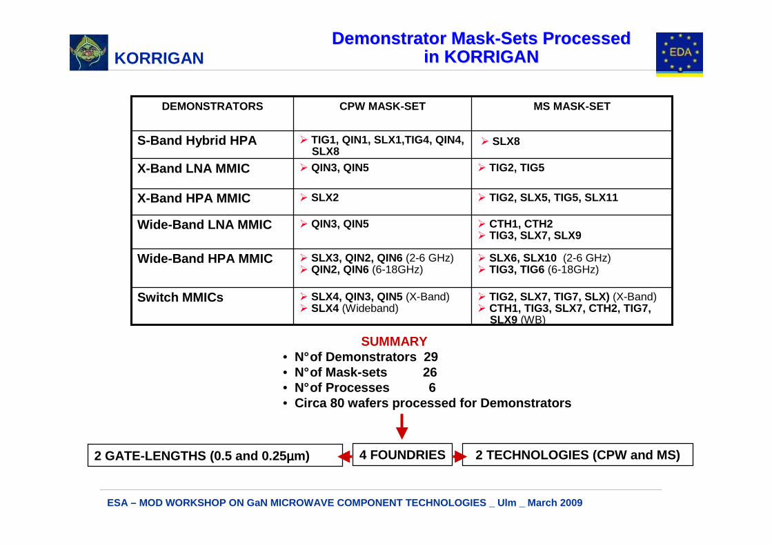
DEMONSTRATORS CPW MASK-SET MS MASK-SET
S-Band Hybrid HPA � TIG1, QIN1, SLX1,TIG4, QIN4,SLX8
� TIG2, TIG5
� TIG2, SLX5, TIG5, SLX11
� CTH1, CTH2� TIG3, SLX7, SLX9
� SLX6, SLX10 (2-6 GHz)� TIG3, TIG6 (6-18GHz)
� TIG2, SLX7, TIG7, SLX) (X-Band)� CTH1, TIG3, SLX7, CTH2, TIG7,
SLX9 (WB)
X-Band LNA MMIC � QIN3, QIN5
X-Band HPA MMIC � SLX2
Wide-Band LNA MMIC � QIN3, QIN5
Wide-Band HPA MMIC � SLX3, QIN2, QIN6 (2-6 GHz)� QIN2, QIN6 (6-18GHz)
Switch MMICs � SLX4, QIN3, QIN5 (X-Band)� SLX4 (Wideband)
Demonstrator MaskDemonstrator Mask --Sets Processed Sets Processed in KORRIGANin KORRIGAN
SUMMARY• N°of Demonstrators 29• N°of Mask-sets 26• N°of Processes 6• Circa 80 wafers processed for Demonstrators
4 FOUNDRIES2 GATE-LENGTHS (0.5 and 0.25 µµµµm) 2 TECHNOLOGIES (CPW and MS)
� SLX8
KORRIGAN
ESA – MOD WORKSHOP ON GaN MICROWAVE COMPONENT TECHNO LOGIES _ Ulm _ March 2009
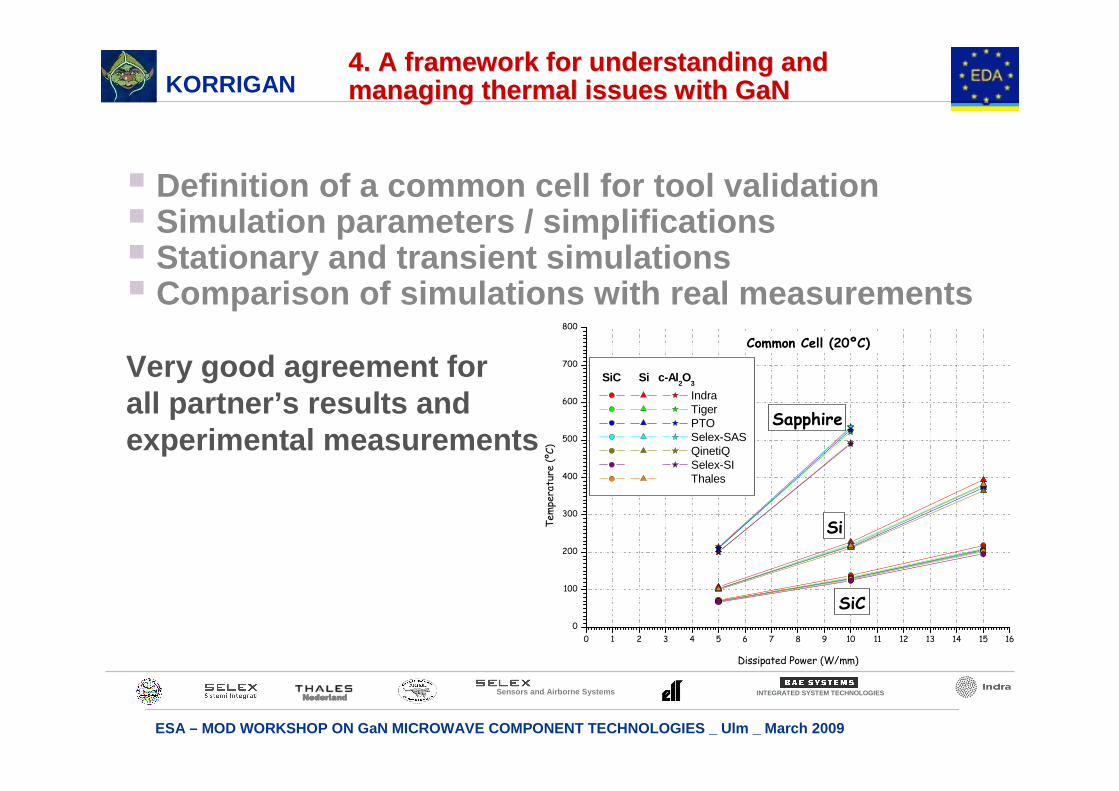
� Definition of a common cell for tool validation� Simulation parameters / simplifications� Stationary and transient simulations� Comparison of simulations with real measurements
Very good agreement forall partner’s results andexperimental measurements
0 1 2 3 4 5 6 7 8 9 10 11 12 13 14 15 16
0
100
200
300
400
500
600
700
800
Sapphire
Si
SiC
SiC Si c-Al2O
3
Indra Tiger PTO Selex-SAS QinetiQ Selex-SI Thales
Common Cell (20ºC)
Tem
perature (ºC
)
Dissipated Power (W/mm)
NederlandNederlandNederlandNederlandSensors and Airborne Systems INTEGRATED SYSTEM TECHNOLOGIES
4. A framework for understanding and 4. A framework for understanding and managing thermal issues with GaNmanaging thermal issues with GaN
KORRIGAN
ESA – MOD WORKSHOP ON GaN MICROWAVE COMPONENT TECHNO LOGIES _ Ulm _ March 2009
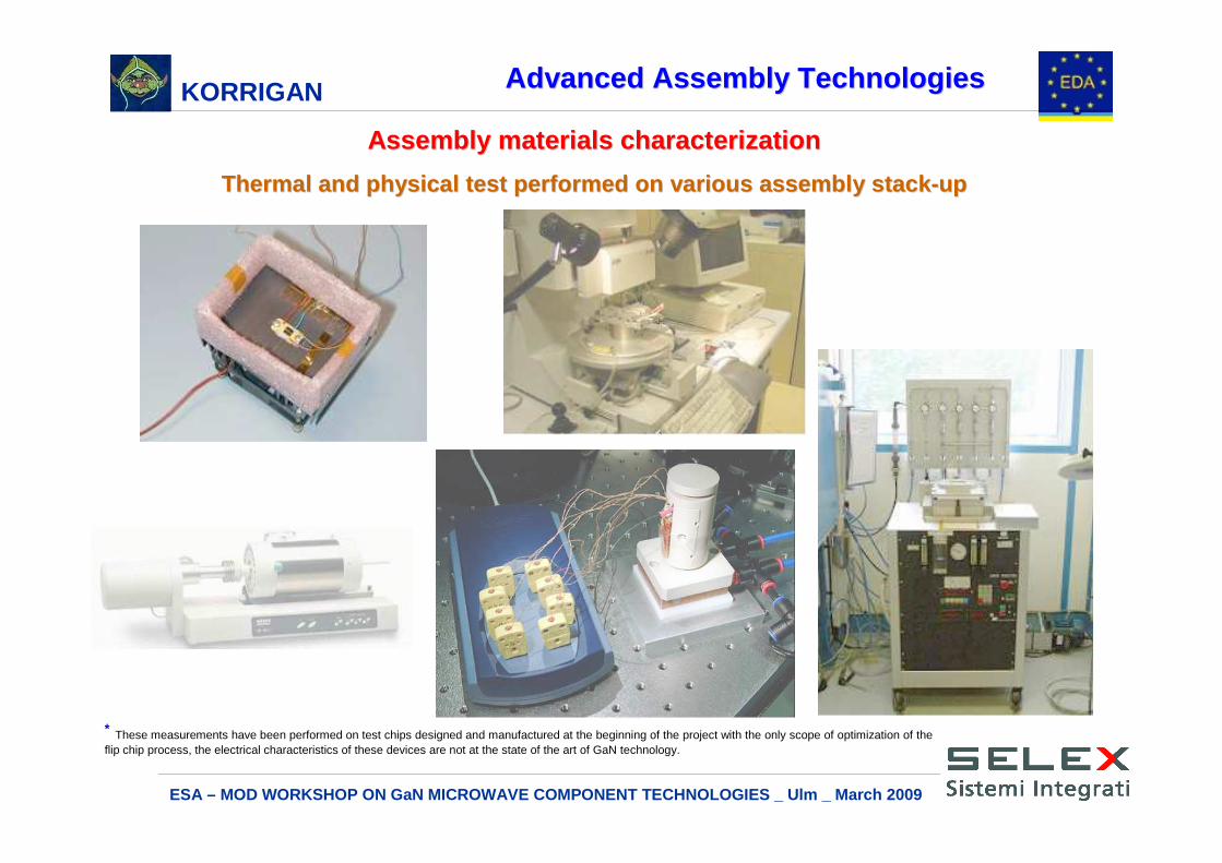
Advanced Assembly TechnologiesAdvanced Assembly Technologies
* These measurements have been performed on test chips designed and manufactured at the beginning of the project with the only scope of optimization of the flip chip process, the electrical characteristics of these devices are not at the state of the art of GaN technology.
Assembly materials characterizationAssembly materials characterization
Thermal and physical test performed on various asse mbly stackThermal and physical test performed on various asse mbly stack --upup
KORRIGAN
ESA – MOD WORKSHOP ON GaN MICROWAVE COMPONENT TECHNO LOGIES _ Ulm _ March 2009
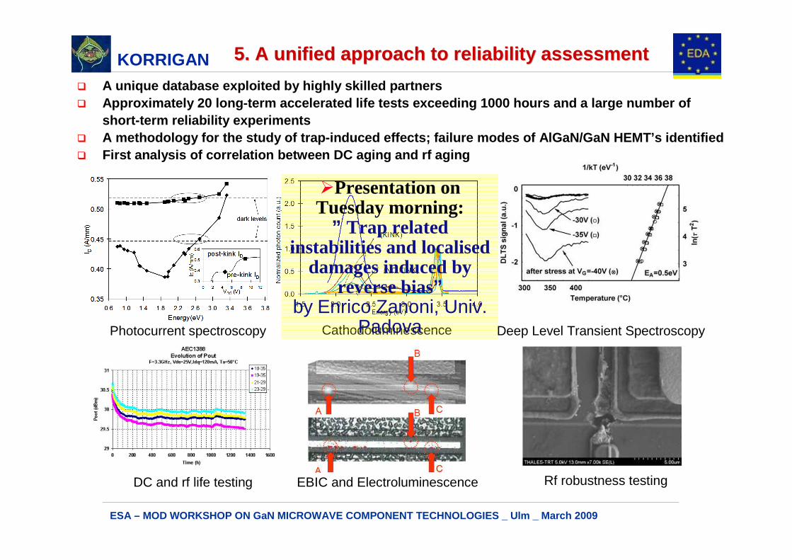
5. A unified approach to reliability assessment5. A unified approach to reliability assessment
Photocurrent spectroscopy Cathodoluminescence Deep Level Transient Spectroscopy
EBIC and Electroluminescence Rf robustness testingDC and rf life testing
� A unique database exploited by highly skilled partn ers� Approximately 20 long-term accelerated life tests e xceeding 1000 hours and a large number of
short-term reliability experiments� A methodology for the study of trap-induced effects ; failure modes of AlGaN/GaN HEMT’s identified � First analysis of correlation between DC aging and rf aging
�Presentation on Tuesday morning:
” Trap related instabilities and localised
damages induced by reverse bias”
by Enrico Zanoni, Univ. Padova
KORRIGAN
ESA – MOD WORKSHOP ON GaN MICROWAVE COMPONENT TECHNO LOGIES _ Ulm _ March 2009
17
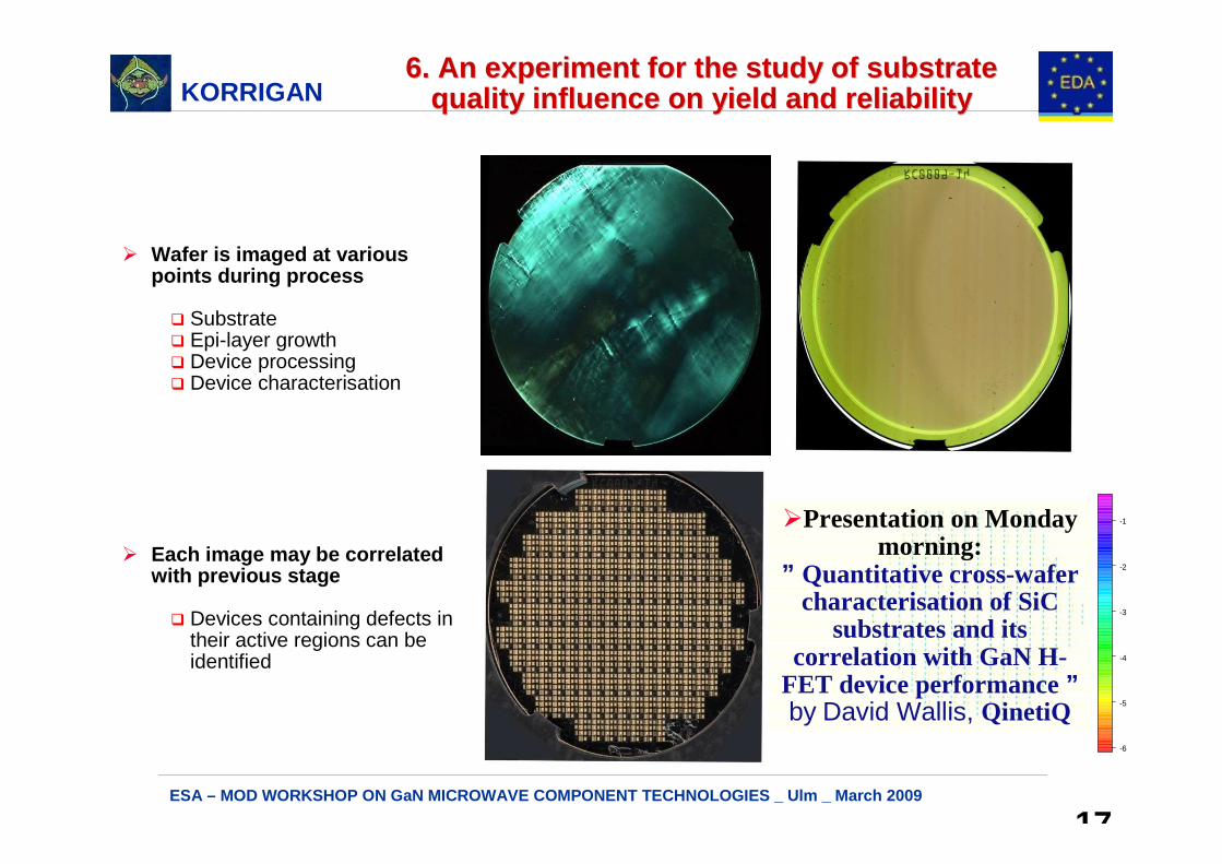
6. An experiment for the study of substrate 6. An experiment for the study of substrate quality influence on yield and reliabilityquality influence on yield and reliability
� Wafer is imaged at various points during process
� Substrate� Epi-layer growth� Device processing� Device characterisation
� Each image may be correlated with previous stage
� Devices containing defects in their active regions can be identified
-6
-5
-4
-3
-2
-1�Presentation on Monday morning:
” Quantitative cross-wafer characterisation of SiC
substrates and its correlation with GaN H-
FET device performance ”by David Wallis, QinetiQ
KORRIGAN
ESA – MOD WORKSHOP ON GaN MICROWAVE COMPONENT TECHNO LOGIES _ Ulm _ March 2009
Conclusion _ Part IConclusion _ Part I
� A robust supply chain has been established, from subs trates through foundries to circuits.
� The establishment of common procedures such as a comm on PCM, design rules and reliability testing allows diff erent processes and devices to be directly compared
�(One question still pending: what about the feedback from ESA about the PCM provided by Korrigan?)
� Models have been established for a wide range of devi ces and processes, and placed on a generally accessible WEB site
� A large database for reliability and parasitic effects is available
GaN in Europe after Korrigan: (6. ) A common approach GaN in Europe after Korrigan: (6. ) A common approach to the development of GaN to the development of GaN FETFET’’’’’’’’ss for microwave systemsfor microwave systems

KORRIGAN
ESA – MOD WORKSHOP ON GaN MICROWAVE COMPONENT TECHNO LOGIES _ Ulm _ March 2009
� There is unified approach to thermal modelling and sim ulation, captured in a common design guide for packaging techn iques and thermal management
� A large number of demonstrator circuits has been design ed and tested, demonstrating in many cases state-of-the-ar t performance, with circuit data made generally available within Europe.
� Korrigan has taken the technology to a stage where circ uit system designers can have a clear view of the potenti al of GaN, detailed guidance on the way the technology is used , and the detailed performance data needed to carry out simulatio ns at the system level.
Conclusion _ Part I (contConclusion _ Part I (cont ’’’’’’’’d)d)
GaN in Europe after Korrigan: A common approach to the GaN in Europe after Korrigan: A common approach to the development of GaN development of GaN FETFET’’’’’’’’ss for microwave systemsfor microwave systems
KORRIGAN
ESA – MOD WORKSHOP ON GaN MICROWAVE COMPONENT TECHNO LOGIES _ Ulm _ March 2009
Conclusion _ Part IIConclusion _ Part II
�A project on substrates / materials already on the tracks
�Ongoing discussion on device-centered follow-up
Prospective for continuation of the effort in EuropeProspective for continuation of the effort in Europe