kelly ip phd defense ~ july 1, 2005 ~ university of florida ~ materials science and enginering...
Post on 19-Dec-2015
214 views
TRANSCRIPT

Kelly IpPhD Defense ~ July 1, 2005
~ University of Florida ~Materials Science and Enginering
Process Development for ZnO-based Devices

~ University of Florida ~ Materials Science and Engineering ~
Outline
Introduction Inductively-coupled plasma (ICP) etching Hydrogen in ZnO Contact metallization
Ohmic contacts Schottky contacts
p-n junction diode Conclusions
~ University of Florida ~ Materials Science and Engineering ~
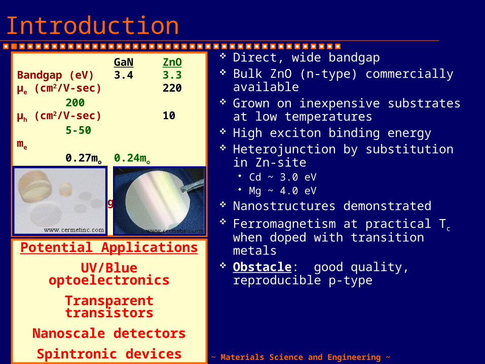
Introduction Direct, wide bandgap Bulk ZnO (n-type) commercially
available Grown on inexpensive substrates at low
temperatures High exciton binding energy Heterojunction by substitution in Zn-site
Cd ~ 3.0 eV Mg ~ 4.0 eV
Nanostructures demonstrated Ferromagnetism at practical Tc when
doped with transition metals Obstacle: good quality, reproducible p-
type
GaN ZnOBandgap (eV) 3.4 3.3µe (cm2/V-sec) 220 200µh (cm2/V-sec) 10 5-50me 0.27mo 0.24mo
mh 0.8mo 0.59mo
Exciton binding 28 60energy (meV)
Potential Applications
UV/Blue optoelectronics
Transparent transistors
Nanoscale detectors
Spintronic devices

~ University of Florida ~ Materials Science and Engineering ~
ICP Etching Wet etching
HCl, HNO3, NH4Cl, and HF Generally isotropic with limited resolution and selectivity
High-density plasma etching Anisotropic with high resolution Favored by modern manufacturing environment
Bulk, wurtzite (0001) ZnO from Eagle-Picher Gas chemistry:
Cl2/Ar (10/5 sccm) & CH4/H2/Ar (3/8/5 sccm) Constant ICP source power at 500W and process pressure
at 1 mTorr Varied rf chuck power: 50 – 300W

~ University of Florida ~ Materials Science and Engineering ~
ICP Etching - Etch Rates
50 100 150 200 250 300
0
1000
2000
3000
4000
5000
Cl2/Ar etch rate
CH4/H
2/Ar etch rate
Etc
h R
ate
(Å/m
in)
RF Power (W)
50
100
150
200
250
300
350 Cl
2/Ar dc bias
CH4/H
2/Ar dc bias
DC
Bia
s (-
V)
CH4/H2/Ar ~3000 Å/min
Cl2/Ar ~1200 Å/min

~ University of Florida ~ Materials Science and Engineering ~
ICP Etching - Etch Mechanism
10 12 14 16 18 200
500
1000
1500
2000
2500
3000
Etc
h R
ate
(Å/m
in)
Square Root (25+Vb)
Cl2/Ar Chemistry
CH4/H
2/Ar Chemisty
Ion-Assisted Etch Mechanism
ER E0.5-ETH0.5
Vapor pressure of etch products:
(CH4)2Zn
301 mTorr at 20°C
ZnCl2
1 mTorr at 428 °C
ETH ~ 96 eV for CH4/H2/Ar

~ University of Florida ~ Materials Science and Engineering ~
ICP Etching - Photoluminescence
2.0 2.5 3.0 3.50.0
0.5
1.0
1.5
2.0
2.5
3.0
50W rf100W rf300W rf200W rf
Control
PL
In
ten
sit
y (
Arb
.)
Energy (eV)
2.0 2.5 3.0 3.5
0.01
0.1
1Control50W rf
100W rf300W rf200W rf
Lo
g P
L In
ten
sity
(A
rb.)
Energy (eV)
Optical degradation even at the lowest rf power

~ University of Florida ~ Materials Science and Engineering ~
ICP - AFM
Control
50 W rf 100 W rf
200 W rf 300 W rf
0 50 100 150 200 250 300
2
4
6
8
Control
ZnOCH
4/H
2/Ar
500W ICP Power
RM
S R
ough
ness
(nm
)
rf Power (W)
Zn and O etch products removed at
same rate
~ University of Florida ~ Materials Science and Engineering ~
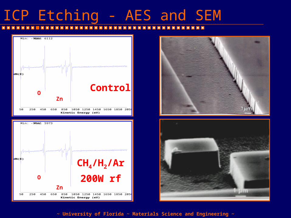
ICP Etching - AES and SEM
Kinetic Energy (eV)
dN(E)
Min: -9203Max: 6112
50 250 450 650 850 1050 1250 1450 1650 1850 2050
Kinetic Energy (eV)
dN(E)
Min: -9742Max: 5973
50 250 450 650 850 1050 1250 1450 1650 1850 2050
CH4/H2/Ar
200W rfO
Zn
Zn
OControl

~ University of Florida ~ Materials Science and Engineering ~
ICP Etching - Summary
Dry etching is possible with practical etch rates using CH4/H2/Ar
Surface is smooth and stoichiometric Anisotropic sidewalls Optical quality is sensitive to ion energy
and flux

~ University of Florida ~ Materials Science and Engineering ~
Hydrogen in ZnO
Hydrogen Predicted role as shallow donor Introduced from growth ambient Present in optimal plasma etch chemistry
Understand diffusion behavior and thermal stability Bulk, wurtzite (0001) ZnO, undoped (n~1017cm-3)
from Eagle-Picher Hydrogen incorporation
Ion Implantation of 2H or 1H (100keV, 1015 - 1016 cm-2) 2H plasma exposure in PECVD at 100-300°C, 30 mins
Post-annealing: 500 - 700°C

~ University of Florida ~ Materials Science and Engineering ~
Hydrogen in ZnO - Implanted - SIMS
0.5 1.0 1.5 2.01015
1016
1017
1018
1019
1020
2H 1015 cm-2 ZnO 5 min anneals
700°C
600°C
500°C
As Implanted
H C
on
cen
tra
tion
(a
tom
s/cm
3 )
Depth (m)
Removal of 2H below SIMS limit at 700°C
Thermally less stable than GaN (>900ºC)

~ University of Florida ~ Materials Science and Engineering ~
0.4 0.6 0.8 1.0 1.2 1.4 1.60
200
400
600
RB
S Y
ield
Energy (MeV)
virgin
11016 cm2
Depth (Å)
100 keV 1H ZnO
10000 7500 5000 2500 0
Hydrogen in ZnO - Implanted - RBS/C
Minimal affect on BS yield near surface
Small increase in scattering peak (6.5% of the random level before implantation and 7.8% after implantation) the
nuclear energy loss profile of 100keV H+ is max

~ University of Florida ~ Materials Science and Engineering ~
Hydrogen in ZnO - Implanted - PL
2.0 2.5 3.0 3.510-3
10-2
10-1
100
101
Control 500 °C 600°C 700°C As-implanted
PL I
nten
sity
(A
rb.)
Energy (eV)
2.0 2.5 3.0 3.5
0.004
0.006
0.008
0.010
0.012
0.014
700°C Anneal600°C Anneal500°C AnnealAs-implanted
PL
Int
ensi
ty (
Arb
.)
Energy (eV)
Severe optical degradation even after 700ºC anneal
Point defect recombination centers dominate

~ University of Florida ~ Materials Science and Engineering ~
Hydrogen in ZnO - Plasma - SIMS
Large diffusion depth 2H diffuses as an interstitial, with little trapping by the lattice elements or by defects or impurities
0 5 10 15 20 25 30
1015
1016
1017
1018
200°C100°C 300°C
2H plasma treatment
Con
cent
ratio
n (a
tom
s/cc
)
Depth (m)

~ University of Florida ~ Materials Science and Engineering ~
Hydrogen in ZnO - Plasma/annealed - SIMS
0 5 10 15 20 25
1015
1016
1017
1018
No anneal
2H plasma 200°CPost treatment anneal
500°C, 5min
400°C, 5min
Con
cent
ratio
n (a
tom
s/cc
)
Depth (m)
2H completely evolve out of the crystal at 500°C

~ University of Florida ~ Materials Science and Engineering ~
Hydrogen in ZnO - Plasma - CV
0.0 0.1 0.2 0.31x10¹⁷
2x10¹⁷
3x10¹⁷
4x10¹⁷
Do
pa
nt C
on
ce
ntr
atio
n (
cm
-3)
Depth (µm)
2H Plasma exposure at 200°C & 600°C Anneal
2H Plasma exposure at 200°C As Grown
Effects 2H plasma treatment
Passivate the compensating acceptor
impurities
Induces a donor state and increases the free electron concentration
Suggest H from growth process
n-type conductivity probably arises from multiple impurity sources

~ University of Florida ~ Materials Science and Engineering ~
Hydrogen in ZnO
0 100 200 300 400 500 600 700
0
20
40
60
80
100
0 200 400 600
1
10
100
% 2 H
Rem
aini
ng
Anneal Temperature (°C)
% 2 H
Rem
aini
ng
Anneal Temperature (°C)
5 min Anneal
Implanted 2H
Plamsa 2H
Implanted 2H is slightly more thermally stable: trapping at residual damage in the ZnO by the
nuclear stopping process
Implanted
Plasma exposure

~ University of Florida ~ Materials Science and Engineering ~
Hydrogen in ZnO - Summary Thermal stability and diffusion behavior of hydrogen in
ZnO T 700 °C completely evolved the implanted H from
ZnO Residual implant-induced defects severely degrade
optical properties and minimal affect crystal structure Plasma: incorporation depths of about 30 m for 0.5 hr
at 300°C T 500 °C to remove H introduced by plasma exposure Thermal stability of the hydrogen retention :
direct implantation > plasma exposure Trapping at residual implant damage

~ University of Florida ~ Materials Science and Engineering ~
Ohmic Contacts
Require low specific contact resistance Surface treatments
As-received Organic solvents (trichloroethylene, methanol,
acetone, 3 mins each) H plasma
Ti/Al/Pt/Au metal scheme on n-type ZnO Bulk PLD films
Au/Ni/Au and Au on p-type ZnMgO

~ University of Florida ~ Materials Science and Engineering ~
Ohmic Contacts - Ti/Al/Pt/Au on Bulk
250 300 350 400 450
2.0x10⁻³
4.0x10⁻³
6.0x10⁻³
8.0x10⁻³
1.0x10⁻²
Spec
ific
Con
tact
Res
isti
vity
(·
cm2 )
Anneal Temperature (°C)
As Received H
2 Plasma
Organic Solvents
Bulk n-ZnO
Metals
Cross-sectional view of circular TLM
R1
RO
ρc lowest at 250 °C anneal ρc ~ 610-4 cm2
Severe contact degradation after 600 °C anneal
)/(
)/(
)/(
)/(ln
2 11
1
11
1
T
TOT
TO
TOO
O
T
O
ST LRK
LRK
R
L
LRI
LRI
R
L
R
RRR
C = RS LT2
Marlow and Das, Solid-State Electron. 25 91 (1982)

~ University of Florida ~ Materials Science and Engineering ~
Ohmic Contacts - Ti/Al/Pt/Au on Bulk - AES

~ University of Florida ~ Materials Science and Engineering ~
Ohmic Contacts - Ti/Al/Pt/Au on Bulk - SEM

~ University of Florida ~ Materials Science and Engineering ~
Ohmic Contacts - Growth: n-type ZnO:P Films N-type phosphorus-doped
ZnO film on (0001) Al2O3 grown by PLD
Post-growth annealing Increase anneal temperature
Decrease carrier concentration and Hall mobility
Increase resistivity Reduction of shallow state
density P dopants activation as
acceptors in O site1016 1017 1018 1019 1020
0
5
10
15
20
Carrier Mobility Resistivity
Carrier Concentration (cm-3)
Car
rier
Mob
ilit
y (c
m2 /V
-s)
10-3
10-2
10-1
100
101
102
103
600 °C
500 °C
450 °C
425 °C
As-grown
Resistivity (
-cm)
Post-growth Anneal T
(°C)
Carrier conc
(#/cm3)Resistivity
(cm)
Hall mobility
(cm2/Vs)
30 1.5 1020 0.002 18.5425 6 1019 0.013 7.8450 2.4 1018 1.3 1.9500 3.2 1017 12.8 1.5600 7.5 1015 463 1.8
Heo et al APL 83 1128 (2003)
Post-growth
Anneal T
(°C)
Carrier conc
(#/cm3)
Resistivity
( cm)
Hall
mobility
(cm2 /Vs)
30 1.5 1020 0.002 18.5
425 6 1019 0.013 7.8
450 2.4 1018 1.3 1.9
500 3.2 1017 12.8 1.5
600 7.5 1015 463 1.8

~ University of Florida ~ Materials Science and Engineering ~
Ohmic Contacts - Ti/Al/Pt/Au ZnO:P Films
1015 1016 1017 1018 1019 1020 1021
10-7
10-6
10-5
10-4
10-3
Spec
ific
Con
tact
Res
ista
nce
(-c
m2 )
Carrier Concentration (cm-3)
As-deposited 200°C anneal,
measured at 30 °C 200°C anneal,
measured at 200°C
Nonalloyed:
n = 1.5 1020 cm-3
c = 8.7 10-7 -cm2
Annealed:Measured at RT:
n = 6.0 1019 cm-3
c = 3.9 10-7 -cm2
Measured at 200 °C
n = 2.4 1018 cm-3
c = 2.2 10-8 -cm2
Ti/Al/Pt/Au (200/800/400/800)Å on PLD ZnO:P films

~ University of Florida ~ Materials Science and Engineering ~
Ohmic Contacts - p-type ZnMgO Films
-0.50 -0.25 0.00 0.25 0.50-0.50
-0.25
0.00
0.25
0.50
Ni/Au (200/800 Å)
No anneal
250 oC
400 oC
500 oC
Cur
rent
(m
A)
Bias (V)
-0.50 -0.25 0.00 0.25 0.50-5.0
-2.5
0.0
2.5
5.0
Ti/Al (200/800 Å)
No anneal
250 oC
400 oC
500 oC
600 oC
Cur
rent
(m
A)
Bias (V)
0 100 200 300 400 500 6000
4000
8000
12000
16000
20000
Ti/Au Ohmic contact Ni/Au Ohmic contact
Res
ista
nce
()
Annealing Temperature (oC)
• Ohmic behavior after annealing 500 °C
• Ti/Au more thermally stable than Ni/Au contacts
• Severe degradation of Ni/Au after 600 °C anneal
S. Kim et al APL 84 1904 (2004)

~ University of Florida ~ Materials Science and Engineering ~
Ohmic Contacts - p-type ZnMgO Films
-5.0 -2.5 0.0 2.5 5.0-0.04
-0.02
0.00
0.02
0.04
600 °C Annealed
As-deposited
Au/Zn0.9
Mg0.1
O:P0.02
Cur
rent
(A
)
Bias (V)
Specific contact resistance after 600 °C anneal
Au: 2.5 10-5 cm2
Au/Ni/Au: 7.6 10-6 cm2
-5.0 -2.5 0.0 2.5 5.0-0.04
-0.02
0.00
0.02
0.04
As-deposited
600 °C Annealed
Au/Ni/Au/Zn0.9
Mg0.1
O:P0.02
Cur
rent
(A
)Bias (V)
~ University of Florida ~ Materials Science and Engineering ~
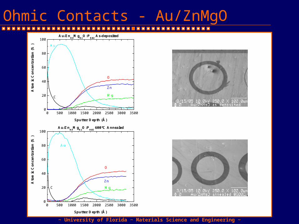
Ohmic Contacts - Au/ZnMgO
0 500 1000 1500 2000 2500 3000 35000
20
40
60
80
100Au/Zn
0.9Mg
0.1O:P
0.02 As-deposited
O
Zn
MgC
Au
A
tom
ic C
once
ntra
tion
(%
)
Sputter Depth (Å)
0 500 1000 1500 2000 2500 3000 35000
20
40
60
80
100Au/Zn
0.9Mg
0.1O:P
0.02 600ºC Annealed
C
Zn
Mg
O
Au
Ato
mic
Con
cent
rati
on (
%)
Sputter Depth (Å)

~ University of Florida ~ Materials Science and Engineering ~
Ohmic Contacts - Au/Ni/Au/ZnMgO
0 500 1000 1500 2000 25000
20
40
60
80
100Au/Ni/Au/Zn
0.9Mg
0.1O:P
0.02 As-deposited
Mg
Ni
C
O
Zn
Au
A
tom
ic C
once
ntra
tion
(%
)
Sputter Depth (Å)
0 500 1000 1500 2000 25000
20
40
60
80
100
Ni
O
Zn
CMg
Au
Au/Ni/Au/Zn0.9
Mg0.1
O:P0.02
600ºC Annealed
Ato
mic
Con
cent
rati
on (
%)
Sputter Depth (Å)

~ University of Florida ~ Materials Science and Engineering ~
Ohmic Contacts - Summary
Ti/Al/Pt/Au to n-type ZnO (bulk, thin film) No significant improvement from H2
plasma treatment or organic solvent cleaning
AES revealed Ti-O interfacial reactions and intermixing between Al and Pt layers T250°C
Au/Ni/Au to p-type ZnMgO: lower C than Au alone

~ University of Florida ~ Materials Science and Engineering ~
Schottky Contacts
Previous Works Metals: Au, Ag, Pd Schottky barriers heights ~ 0.6-0.8 eV Barrier heights not following the difference in the
work function value interface defect states determine contact characteristics
Au is unstable even at 60°C This Work Investigate the effect of UV surface cleaning Metal schemes:
PLD n-type film: Pt Bulk: Pt, W, W2B, W2B5, CrB2

~ University of Florida ~ Materials Science and Engineering ~
Schottky Contacts - Pt/Au on Bulk
No ozone treatment: Linear I-V Ozone treatment:
B = 0.696 eV
= 1.49 Js = 6.17 10-6 A-cm-2
-0.10 -0.05 0.00 0.05 0.10-1.0
-0.5
0.0
0.5
1.0
No ozone
Cur
rent
(m
A)
Bias (V)
0.0 0.1 0.2 0.3 0.4 0.50.000
0.005
0.010
0.015
0.020
B = 0.696 eV
= 1.49
Js = 6.17 10-6 A-cm-2
30 min ozone
Cur
rent
(A
)
Bias (V)
-10 -8 -6 -4 -2 0-3.0
-2.5
-2.0
-1.5
-1.0
-0.5
0.0
30 min ozone
Cur
rent
(m
A)
Bias (V)

~ University of Florida ~ Materials Science and Engineering ~
Schottky Contacts - UV Ozone - AFM
No Ozone Treatment
30 min Ozone Treatment

~ University of Florida ~ Materials Science and Engineering ~
Schottky Contacts - UV Ozone - XPS
1000 800 600 400 200 0-60000
-40000
-20000
0
20000
40000
60000No Ozone
ZnCO
O
Zn
Zn
N(E
)
Energy (eV)
C 1s peak No ozone (at. %) 30 min (at.%)
No Ar+ sputter 29.5 5.8
1 min Ar+ sputter 5.3 1.1
2 min Ar+ sputter 2.6 0.1
1000 800 600 400 200 0
-100000
-50000
0
50000
100000
150000
CO Zn
Zn
Zn
30 min Ozone
N(E
)
Energy (eV)
Desorption of
surface C
contaminants

~ University of Florida ~ Materials Science and Engineering ~
Schottky Contacts - W/Pt/Au on Bulk
-0.4 -0.2 0.0 0.2 0.4-0.1
0.0
0.1
0.2
0.3
Cur
rent
(m
A)
Bias (V)
700 °C, 1 min anneal 30 min ozone No ozone
-0.010 -0.005 0.000 0.005 0.010
-1.0
-0.5
0.0
0.5
1.0
Cur
rent
(m
A)
Bias (V)
As-sputtered 30 min ozone no ozone
Sputter-induced damages Non-rectifying for 250
°C and 500 °C anneal Rectifying after 700 °C
anneal
No ozone 30 min ozone
B (eV) 0.45 0.49
4.5 3.2
Js (A-cm-2) 8.4310-2 2.1110-2

~ University of Florida ~ Materials Science and Engineering ~
Schottky Contacts - W/Pt/Au - AES
0 200 400 600 800 10000
5000
10000
15000
20000
25000
30000
O
Zn
W
PtAu
C
30 min ozone, as-sputtered
Inte
nsit
y (a
rb. u
nit)
Time (s)
0 200 400 600 800 10000
5000
10000
15000
20000
25000
Zn
Zn
W
AuPt
C O
30 min ozone, 700 °C anneal
Inte
nsit
y (a
rb. u
nit)
Time (s)
• Post-deposition annealing 500 °C: no detectable intermixing
• 700 C anneal: Zn diffused out to the Au-Pt interface, independent of whether the samples had been exposed to ozone

~ University of Florida ~ Materials Science and Engineering ~
Schottky Contacts - W2B5 vs. W2BW2B5/Pt/Au as deposited
W2B5/Pt/Au 600ºC annealed
W2B/Pt/Au as deposited
W2B/Pt/Au 600ºC annealed

~ University of Florida ~ Materials Science and Engineering ~
Schottky Contacts - Summary
Ozone treatment removes surface C contamination Pt contacts: ozone treatment produces transition
from ohmic to rectifying behavior W contacts: require annealing T 700°C to repair
sputter-induced damages AES revealed intermixing of metal layers and out-
diffusion of Zn to Au-Pt interface Low barrier heights for boride contacts W2B showed good thermal stability high
temperature ohmic contacts

~ University of Florida ~ Materials Science and Engineering ~
p-n Junction Diode - Growth and Structure
Full backside ohmic contact
Bulk ZnO (0.5 mm, n ~ 1017 cm-3)
Buffer n-ZnO PLD film (~0.8 m)
Zn0.9Mg0.1O: P0.02 PLD film (~1.4 m)
Circular ohmic contact (50 to 375 m diameter)
Pulsed laser deposition (PLD)
(0001) bulk ZnO substrate
Zn0.9Mg0.01O:P0.02 target
KrF excimer laser ablation sourceLaser repetition rate: 1 Hz
Laser pulse energy density: 3 J-cm-2
Growth: 400 °C, O2 overpressure of 20 mTorr
Ohmic contacts: p-ZnMgO: Pt/Au (200/800Å)
n-ZnO: Ti/Al/Pt/Au 200/400/200/800Å)
Annealed at 200 °C, 1 min, N2 ambient
Undoped buffer layer necessary for good rectifying behavior

~ University of Florida ~ Materials Science and Engineering ~
p-n Junction Diode - IV Characteristics
-10.0 -7.5 -5.0 -2.5 0.0 2.5 5.0-0.04
-0.02
0.00
0.02
0.04
Pt/Au 50 m Diode
Cur
rent
(A
)
Bias (V)
Measured at room temp:
VRB –9.0 V
Js 4.610-9 A·cm-2
Vf 4.0 V
RON 14.5 m ·cm-2

~ University of Florida ~ Materials Science and Engineering ~
p-n Junction Diode - Reverse Breakdown
-8 -6 -4 -2 0-0.04
-0.03
-0.02
-0.01
0.00
Cur
rent
(A
)
Bias (V)
Pt/Au 210 m diodeMeasurement Temperatures
30 °C 50 °C 100 °C 150 °C 200 °C
0 50 100 150 200 2501
2
3
4
5
6
7
Pt/Au
Rev
erse
Bre
akdo
wn
Vol
tage
(V
)
Measurement Temperature (°C)
)](1[ 00 TTVV RBRB
Temperature coefficient:Slightly negative ~ .1 to .2 V/K
Presence of defects
Non-optimized growth and processing

~ University of Florida ~ Materials Science and Engineering ~
p-n Junction Diode - Summary
Demonstrated ZnO-based p-n junctions ZnMgO/ZnO heterostructure system n-type ZnO buffer on the ZnO substrate is critical
in achieving acceptable rectification in the junctions
Important step in realizing minority carrier devices in the ZnO system

~ University of Florida ~ Materials Science and Engineering ~
Conclusions ICP etching
Methane-based chemistry Practical etch rate but optical degradation
H in ZnO Much less thermally stable than GaN Completely evolve out by 700°C anneals
Ohmic contacts to ZnO Straightforward n-type Rapidly improving for p-type
Schottky contacts to ZnO Low B for both n-type and p-type Surface states dominate transport mechanism
p-n junction diode using ZnMgO/ZnO demonstrated

~ University of Florida ~ Materials Science and Engineering ~
Acknowledgements
Committee members: Prof. Stephen Pearton, Chair Prof. Cammy Abernathy Prof. David Norton Prof. Rajiv Singh Prof. Fan Ren, External
Contributors:Y.-W. Heo Y. Li B. Luo
B.P. Gila E.S. Lambers K.H. Baik
A.H. Onstine M.E. Overberg J.R. LaRoche