july 4th-8th 2011, ipn lyon - 8th international conference...
TRANSCRIPT

ElectronicsElectronics for for PhotodetectorsPhotodetectors
Jean-Francois
GenatLPNHE Paris
New Developments
In PhotodetectionJuly 4th-8th 2011, IPN Lyon
[email protected] 44 27 22 37

ThanksThanks toto
Christophe de la TailleJacques Lecoq
Eric OberlaEric DelagnesHervé Grabas
Dominique BretonThanh Hung Pham
Hervé LebboloKholdoun Torki
and many others…

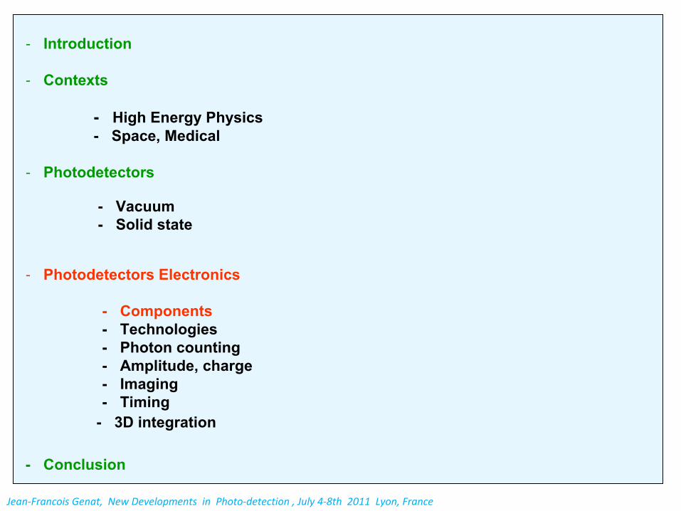
- Introduction
- Contexts
-
High Energy
Physics-
Space, Medical
- Photodetectors
-
Vacuum-
Solid
state
- Photodetectors
Electronics
-
Technologies, -
Photon counting-
Amplitude, charge-
Imaging- Timing-
3D integration
- Conclusion
Jean‐Francois Genat, New Developments in Photo‐detection, July 4‐8th 2011 Lyon, France

4
IntroductionElectromagnetic
wave
= photon
‐
Electromagnetic
wave:
Wavelength
, Maxwell’s
equations
‐
Photon:Photon wavelength
hc/
Schrodinger’s
equation
(Electromagnetic
field)2
:photon’s
probability
of presence
Wikipedia
http://www.cft.edu.pl/~birula/publ/CQO7.pdf
1eV 1.2m 2.414 Hz Near Infra-red photon
Jean‐Francois Genat, New Developments in Photo‐detection, July 4‐8th 2011 Lyon, France

5
Photon Electron interaction
Photon-atom
interaction:
-
No absorption : Rayleigh elastic
scattering
no electron
ejected
- Energy
change, absorption:
-
Compton effect:
photon scattered
with
wavelength
change electron
ejected
-
e+ e-
pairs generation
(
rays): 2 x 511 keV
minimum energy
«
Shower
»
in a «
radiator
»
measured
in a (photo)-detector
h
Jean‐Francois Genat, New Developments in Photo‐detection, July 4‐8th 2011 Lyon, France

Photo-detectorsVacuum devices
‐
Photo‐Multipliers Tubes (PMTs)‐
Hybrid Photo‐diodes (HPDs)
‐
Micro‐Channel Plates (MCPs)
Solid state devices
‐
Charge Coupled Devices (CCDs)‐
Avalanche Photo‐diodes (APDs)
‐
Silicon Photo‐multipliers, (SiPMs, Geiger mode APDs)‐
Monolithic
Active Pixel Sensors (MAPS, CMOS Silicon)
Hybrids
- Hybrid APDs (HPD/APD)- Electron Bombarded CMOS (HPD/MAPS)
Jean‐Francois Genat, New Developments in Photo‐detection, July 4‐8th 2011 Lyon, France

Vacuum devicesCurrent signal from electrons in vacuum
‐
Large area, large fill factor, poor QE
‐
Full‐custom Photo‐cathode
‐
Electron multiplication, high gain, fast
‐
Low noise (photo‐cathode noise)
‐
Some sensitivity to magnetic fields (depends on device)
‐
Readout with external ASICs
Solid state semi‐conductor devicesCurrent signal from e-/holes + avalanche in ½ conductor
‐
Size limited to a wafer, limited filling factor, high QE
‐
Spectral response of ½
conductor (Si, GaAs, HgCdTe…)
‐
Multiplication in high electric fields (depleted PN junctions)
‐
Noisy due to reverse currents avalanches
‐
Noise very sensitive to irradiation
‐
No sensitivity to magnetic field
‐
Readout easy to integrate + 3D availability
Vacuum and Solid-state
Jean‐Francois Genat, New Developments in Photo‐detection, July 4‐8th 2011 Lyon, France

Vacuum devices
Photo‐multipliersHybrid photo‐diodes (HPDs)Electron bombarded CMOSMicro‐Channel Plates
Solid state (semi‐conductor) devices
Avalanche Photo-diodesSilicon PMs
Hybrids Electron bombarded Silicon
Devices
Jean‐Francois Genat, New Developments in Photo‐detection, July 4‐8th 2011 Lyon, France

9
Silicon PMs
From B. Dolgoshein
et al. 25 m MCP from P. Hink
(Burle‐Photonis)
Vacuum devicesSingle photo‐electrons signals
Silicon Photo‐Multipliers (SiPM), Micro‐channel Plates (MCP)
25 microns, MCP from Burle-Photonis
Jean‐Francois Genat, New Developments in Photo‐detection, July 4‐8th 2011 Lyon, France

Signal development
-
Current
signals
occur
as long as charges move in the detector gap
Rise time is RC dependent at first order sets the electronics bandwidth for timing
Serial noise proportional to CR small, 50
or less if a common base preamp is used
Electronics should not increase C (cables, connectors...)C is the capacitance seen during the rising edge (not a full coaxial cable length)
Effect of first order passive:
Step response:
)]/exp(1[)( 01 RCtiti
)()()(0 tvtnqti
Jean‐Francois Genat, New Developments in Photo‐detection, July 4‐8th 2011 Lyon, France

Signal development (½ conductor)
Two
types of carriers:
-
Electrons-
Holes, 3 times slower
in silicon-
75 electrons-holes
in one micron
- APDs
and SiPMs:
-
Avalanche process
is
very
fast, RC is
observed
in practice
Reduce
R using
a transimpedance
or a current
conveyor
input stage
)]RC/texp()][t(i)t(i[()t(i he 11
Jean‐Francois Genat, New Developments in Photo‐detection, July 4‐8th 2011 Lyon, France

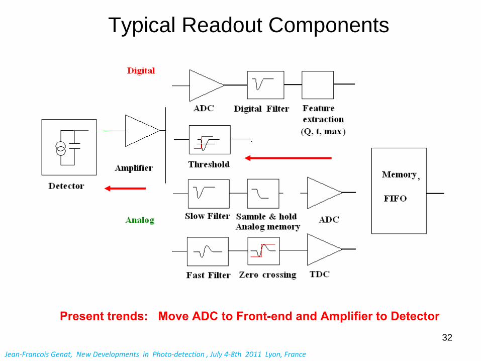
Electronics and Signal Processing
‐ Not much amplification needed with PMTs, MCPs, SiPMTs1 electron is 5mV in 50with a detector gain of 106‐7Or current conveying using common base input stage
‐ Amplification for 103
to 106
detector gains of (G)APDs, CCDs
‐
Filtering: “Pulse shaping”
to remove amplifier noise out of
the signal’s frequency content
‐ Digitization: Convert to a sequence of numbers using ADCs
‐ Feature extraction: get time, amplitude, charge…Can digital filter as well, remove pedestals
‐
Send results to user: normalize, compress, error recover…
Detector model
Jean‐Francois Genat, New Developments in Photo‐detection, July 4‐8th 2011 Lyon, France

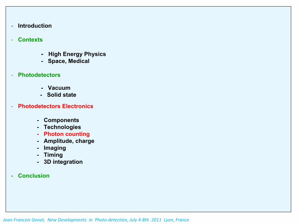
- Introduction
- Contexts
-
High Energy
Physics-
Space, Medical
- Photodetectors
- Vacuum-
Solid
state
- Photodetectors
Electronics
-
Technologies-
Photon counting-
Amplitude, charge-
Imaging-
Timing-
3D integration
-
Conclusion
Jean‐Francois Genat, New Developments in Photo‐detection, July 4‐8th 2011 Lyon, France
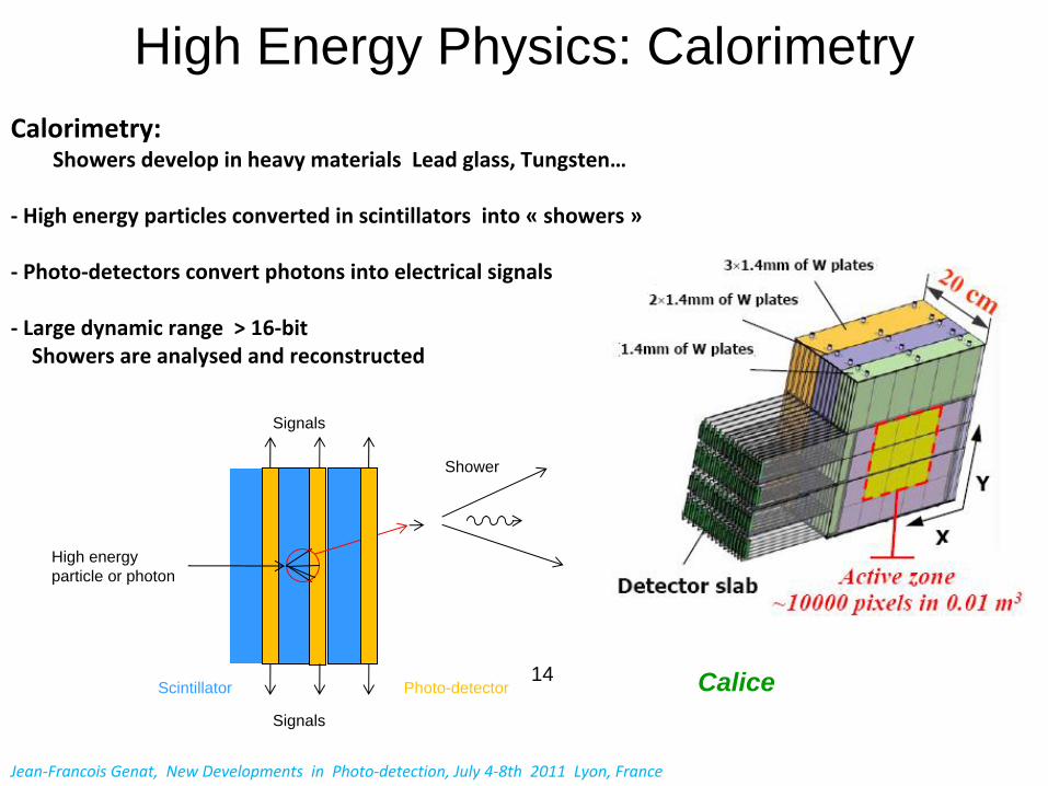
14
High Energy Physics: CalorimetryCalorimetry:
Showers
develop
in heavy
materials
Lead
glass, Tungsten…
‐
High energy
particles
converted
in scintillators
into
«
showers
»
‐
Photo‐detectors convert
photons into
electrical
signals
‐
Large dynamic
range > 16‐bitShowers
are analysed
and reconstructed
High energyparticle or photon
Photo-detectorScintillator
Signals
Signals
Shower
Calice
Jean‐Francois Genat, New Developments in Photo‐detection, July 4‐8th 2011 Lyon, France

ATLAS Hadron Calorimeter ATLAS TileCal
15
Constraints for the front-end electronics
-
Photo-multipliers rise time : 5 ns -
Least significant charge: 25 fC
(20 MeV muon)
-
Largest charge: 1.6 nC
-
For noise and LSB of 12,5 fC-
The corresponding currents are:
-
625 nA
LSB-
Max: 40mA
Large dynamic range, 16-bits
A multi-gain design is required
Jean‐Francois Genat, New Developments in Photo‐detection, July 4‐8th 2011 Lyon, France

New photo-detectors for Calorimeters Solid-state
9 March 2011ACES 2011 J. Nash CMS Upgrade Plans
16
Array of avalanche photo diodes: “digital”
photon detection
Array can be 0.5x0.5 up to 5.0x5.0 mm2
Pixel size can be 10 up to 100m
All APDs
connect to a single output
Signal = sum of all cells
Advantages over HPDs:
28% QE (x2 higher) and 106
gain (x500 higher)
More light (40 pe/GeV), less photo-statistics broadening
Very high gain can be used to give timing shaping/filtering
Jean‐Francois Genat, New Developments in Photo‐detection, July 4‐8th 2011 Lyon, France
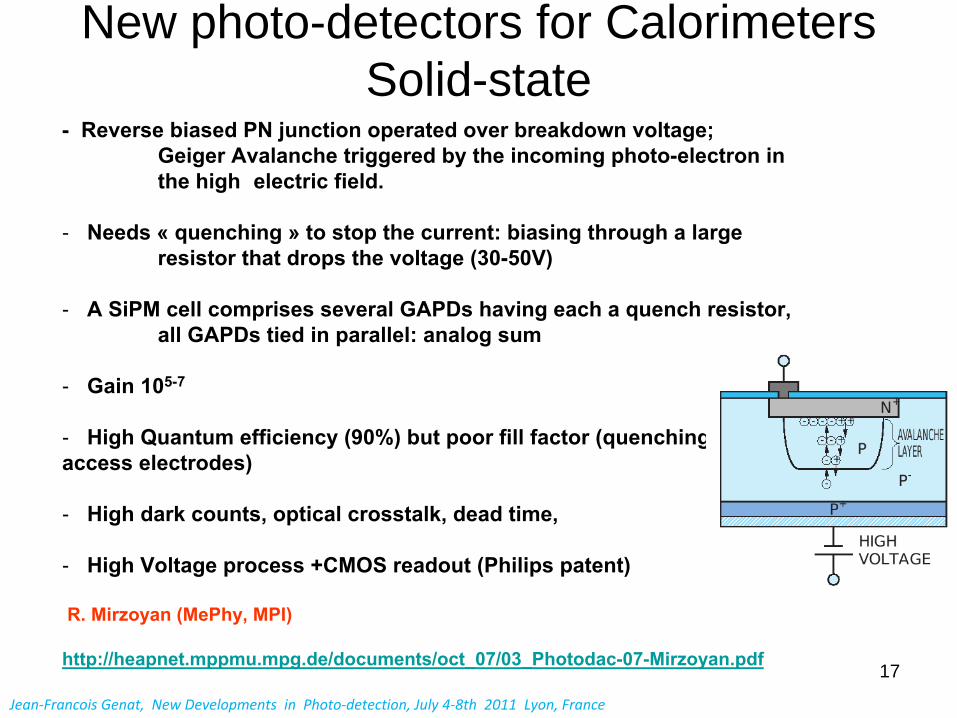
New photo-detectors for Calorimeters Solid-state
17
Jean‐Francois Genat, New Developments in Photo‐detection, July 4‐8th 2011 Lyon, France
-
Reverse biased
PN junction
operated
over breakdown voltage; Geiger Avalanche triggered
by the incoming
photo-electron
in the high
electric
field.
- Needs
«
quenching
»
to stop the current: biasing
through
a large resistor
that
drops the voltage (30-50V)
- A SiPM
cell
comprises several
GAPDs
having
each
a quench
resistor, all GAPDs
tied
in parallel: analog
sum
- Gain 105-7
- High Quantum efficiency
(90%) but poor
fill
factor (quenching
resistor, access
electrodes)
- High dark
counts, optical
crosstalk, dead
time,
- High Voltage process
+CMOS readout
(Philips patent)
R. Mirzoyan
(MePhy, MPI)
http://heapnet.mppmu.mpg.de/documents/oct_07/03_Photodac-07-Mirzoyan.pdf

18
High Energy Physics: Particle ID
Particle
Identification:
- Cerenkov counters: cos v/c
High energyparticle or photon
Scintillator
Improved
with
100ps resolution
Time of Flight
Jean‐Francois Genat, New Developments in Photo‐detection, July 4‐8th 2011 Lyon, France
SPECIFICATION ACTUAL
Sampling Rate 500 MS/s-17GS/s 2.5 GSa/s-17GS/s
# Channels 4 4
Sampling Depth 256 cells 256 Cells
Sampling Window 256*(Sampling Rate)-1
256*(Sampling Rate)-1
Input Noise 1 mV RMS 1-1.5 mV RMS
Analog Bandwidth 1.5 GHz Average 600 MHz
ADC conversion Up to 12 bit @ 2GHz
Up to ~10 bit @ 2GHz
Latency 2 µs (min) – 16 µs (max)
3 µs (min) – 30 µs (max)
Internal Trigger yes yes
Example:
Fast
timing readout
using
10 GS/sAnalog
Memory ASIC (SCA):

- Introduction
- Contexts
-
High Energy
Physics-
Space, Medical
- Photodetectors
-
Vacuum-
Solid
state
- Photodetectors
Electronics
-
Components-
Technologies-
Photon counting-
Amplitude, charge - Imaging-
Timing- 3D integration
-
Conclusion
Jean‐Francois Genat, New Developments in Photo‐detection , July 4‐8th 2011 Lyon, France

20
Space applicationsImagers
Space
boarded
Telescopes
Need
to observe single photons with
fair
position resolutionin all spectral domains, in particular
(near
to far) infra-red
Pixellated
devices
such
as Charge Coupled
Devices, Photo-detectors can
be:
-
Silicon
in the visible -
Compounds materials
-
CdTe
for soft Xrays-
CdZnTe
for hard Xrays-
InGaAs
for near
IR-
HgCdTe
for far IR
Pixels as small
as 5 x 5 m, can
be
instrumented.Passive (CCDs) or active (Active Pixel Sensors)
Space
boarded
X ray detectors for imaging
and spectrometryhttp://www.jwst.nasa.gov/
JWST
JWST Focal Plane ArrayJean‐Francois Genat, New Developments in Photo‐detection, July 4‐8th 2011 Lyon, France
«
Asynchronous
»
events
(no trigger)
- Introduction
- Contexts
-
High Energy
Physics-
Space, Medical
- Photodetectors
- Vacuum-
Solid
state
- Photodetectors
Electronics
-
Components-
Technologies-
Photon counting-
Amplitude, charge - Imaging-
Timing- 3D integration
-
Conclusion
Jean‐Francois Genat, New Developments in Photo‐detection, July 4‐8th 2011 Lyon, France

PET CT High/low
Jean‐Francois Genat, New Developments in Photo‐detection, July 4‐8th 2011 Lyon, France
«
Asynchronous
»
events
(no trigger)

Combined
PET-CT
Jean‐Francois Genat, New Developments in Photo‐detection, July 4‐8th 2011 Lyon, France
PET + CT TOF-PET
W.W. MosesAREVA
«
Asynchronous
»
events
(no trigger)

- Introduction
- Contexts
-
High Energy
Physics-
Space, Medical
- Photodetectors
-
Vacuum- Solid state
- Photodetectors
Electronics
-
Components-
Technologies-
Photon counting-
Amplitude, charge -
Imaging- Timing-
3D integration
- Conclusion
Jean‐Francois Genat, New Developments in Photo‐detection, July 4‐8th 2011 Lyon, France

25
Timing-Imaging Device (visible)Multi-anodes PMTs Hybrid Photo-Diodes Silicon-PMTs Micro-Channel Plates
Dynodes Electrons on Silicon Quenched Geiger Micro-PoresEBCMOS
Quantum Eff. 25% 25% 90% 25% Collection Eff. 90% 90% 70% 70%Gain 106 102-4 106 106
Rise-time 1-5ns 1-5ns 250ps 50-500psTiming resolution (1PE) 150ps 100ps 100ps 20-30psPixel size 2x2mm2 10x10m2 50x50m2 1.5x1.5mm2
Dark counts 1-10Hz/cm2 1Hz-40kHz/cm2
1-10MHz/pixel 1Hz-1kHz/cm2
Dead time 5ns 100-500ns 1sMagnetic field no 1.5T yes 1.5TRadiation hardness 1kRad=noisex10 good (glass, Al2 O3 )
Jean‐Francois Genat, New Developments in Photo‐detection, July 4‐8th 2011 Lyon, France

- Introduction
- Contexts
-
High Energy
Physics-
Space, Medical
- Photodetectors
-
Vacuum- Solid state
- Photodetectors
Electronics
-
Components-
Technologies-
Photon counting-
Amplitude, charge -
Imaging- Timing-
3D integration
- Conclusion
Jean‐Francois Genat, New Developments in Photo‐detection, July 4‐8th 2011 Lyon, France

Large Area Micro-Channel Plates20 x 20 cm2 MCP structure:
-
Custom photo-cathode
-
2-plate chevron (high
gain)
-
Transmission line 2D readout
limit
the number
of electronics
channels
Electronics:-
GS/s Flipped-Chip ASICs:
Waveform
Sampling
+ Digital Signal Processing
Jean‐Francois Genat, New Developments in Photo‐detection , July 4‐8th 2011 Lyon, France

2828
Micro-Channel Plate Signals
The fastest photo-detector to date
From Photek
Jean‐Francois Genat, New Developments in Photo‐detection , July 4‐8th 2011 Lyon, France
- Introduction
- Contexts
-
High Energy
Physics-
Space- Medical
- Photodetectors
- Vacuum-
Solid
state
- Photodetectors
Electronics
-
Components-
Technologies-
Photon counting-
Amplitude, charge - Imaging-
Timing- 3D integration
-
Conclusion
Jean‐Francois Genat, New Developments in Photo‐detection , July 4‐8th 2011 Lyon, France

• Bias: ABOVE breakdown
• Geiger-mode: it’s a TRIGGER device!!
• Gain: meaningless ... or “infinite” !!
• Bias: slightly BELOW breakdown
• Linear-mode: it’s an AMPLIFIER
• Gain: limited < 1000
Proportional mode Geiger-mode
Multiplication
initiated
by
electron‐hole,
thermally
or
induced
within
the
APD
and
accelerated in the high electric field at the APD junction.
APDs
A. Dieguez (U Barcelona)
Jean‐Francois Genat, New Developments in Photo‐detection , July 4‐8th 2011 Lyon, France
- Introduction
- Contexts
-
High Energy
Physics-
Space, Medical
- Photodetectors
-
Vacuum- Solid state
- Photodetectors
Electronics
-
Components-
Technologies-
Photon counting-
Amplitude, charge -
Imaging- Timing
-
3D integration
- Conclusion
Jean‐Francois Genat, New Developments in Photo‐detection , July 4‐8th 2011 Lyon, France
32
Typical Readout Components
Present
trends: Move ADC to Front-end and Amplifier to Detector
Jean‐Francois Genat, New Developments in Photo‐detection , July 4‐8th 2011 Lyon, France

- Introduction
- Contexts
-
High Energy
Physics-
Space, Medical
- Photodetectors
- Vacuum-
Solid
state
- Photodetectors
Electronics
- -
Components-
Technologies-
Photon counting-
Amplitude, charge-
Imaging-
Timing-
3D integration
-
Conclusion
Jean‐Francois Genat, New Developments in Photo‐detection , July 4‐8th 2011 Lyon, France

34
Technologies
Jean‐Francois Genat, New Developments in Photo‐detection, July 4‐8th 2011 Lyon, France
Best results
in analog
design:ASIC implementation
at
the transistor level
Position resolution
requires
smaller
pixelsIncreased
on-pixel signal processing
up to ADCs
Thinner
feature
size processes
(65nm and less
are coming…)
Available
technologies:
-
Standard Deep
Sub-Micron CMOS down to 65nm-
High voltage CMOS
Large dynamic
range readout
(but multi-gain possible with
std
CMOS) CCD clocks
generation
-
Silicon
Germanium (SiGe) for faster
and low
1/f noise applications-
Higher
mobility
(GBW=300GHz)-
Larger
current
gain (beta) -
CMOS compatible (0.25 or 0.35μm) for mixed-signal design

35
ASICs feature sizeThe smaller
the components, the faster, the less
power, the greater
density
BW = 1/2RC, Wc
= CV2
ENC 1/Cdet
Reduce
capacitances wherever
possible
But reduced
dynamic
rangesince
voltage supply
decreases
Vdd
= 1.2-1.6V in 65nmMulti Vdd
– Multi Vt
technologies
Multi-gain designs
Moore’s
law: 1968Computing
power will
double every
two
years, for approximately
the same
cost
Intel
Jean‐Francois Genat, New Developments in Photo‐detection, July 4‐8th 2011 Lyon, France

36
ASICs integration level
The smaller
the components, the faster, the less
power, the greater
density:
BW = 1/2RC, W c
= ½
CV2
Reduce
capacitances wherever
possibleReduce
device
feature
size
Wikipedia
Jean‐Francois Genat, New Developments in Photo‐detection, July 4‐8th 2011 Lyon, France

37
Noise vs Technology
Christophe de la Taille
Jean‐Francois Genat, New Developments in Photo‐detection, July 4‐8th 2011 Lyon, France

38
Noise vs gate length
M. Manghisoni
Jean‐Francois Genat, New Developments in Photo‐detection, July 4‐8th 2011 Lyon, France
Noise spectral densities
for 90nm at
L= 700, 350, 130nm

39
ASICs CostsCosts
of MPW (Source: Europractice)
http://www.europractice-ic.com
Process Feature
Cost
Eur/mm2
CMOS 180nm 0.6k UMC180nm HV 50V 1.2k AMS130nm 1.1k UMC
90nm 2.8kCMOS 350nm Opto
0.7k
AMSSiGe
350nm 0.9k AMS250nm 30 GHz
1.9k IHP180
4.4k130nm+ CMOS 300 5.4k
IHP400
6.0k
50-100 parts / MPW runSome
minimum area (25, 16, 12 mm required)
Masks
(production): 100-200k
PackagingCeramic: 20-30€/chipPlastic : 2k€
+ 1-2 €/chipJean‐Francois Genat, New Developments in Photo‐detection, July 4‐8th 2011 Lyon, France
- Introduction
- Contexts
-
High Energy
Physics-
Space, Medical
- Photodetectors
- Vacuum-
Solid
state
- Photodetectors
Electronics
-
Components-
Technologies-
Photon counting-
Amplitude, charge-
Imaging-
Timing-
3D integration
-
Conclusion
Jean‐Francois Genat, New Developments in Photo‐detection, July 4‐8th 2011 Lyon, France

41
Photon CountingSpace and Medical application: no trigger, asynchronous recordingHigh Energy Physics: a beam synchronous signal is usually available
Visible photons have 1 –
3 eV
energy
-
Photo-cathodes have QEs
of 30% at best-
In semi-conductors, gap is 1.12 eV
for Silicon, 1.4 eV
for GaAs
Only 1 electron-hole pair per photon
Single photon counting, noise below 1 electron
Jean‐Francois Genat, New Developments in Photo‐detection, July 4‐8th 2011 Lyon, France
Silicon
PM and Vacuum PMTresponses
compared
http://hepnp.ihep.ac.cn/qikan/manage/wenzhang/20110111.pdf

42
Silicon PMs (Geiger-APDs) readout
Quenching resistor: high value NMOS transistorInhibit / Reset switches
Switch sensing node to Vdd
/ Gnd
Inv Shaping to logic levelsLatch
Memorize Inv state on clk1
Clk2
enable latch on the output bus
E. Villela
et al. NIM A 2010 Readout
electronics
for low
dark
count pixel detectors
Jean‐Francois Genat, New Developments in Photo‐detection, July 4‐8th 2011 Lyon, France

43
Medipix (EUDET)
MEDIPIX1-3 :
Readout chip to be bonded to an imaging semi-conductor detector (X rays)
-
Asynchronous for photon counting, - Time over threshold provides raw
energy estimate
MEDIPIX3: Dead-timeless readout ( two counters, one counts, one is read)
MEDIPIX Website
Jean‐Francois Genat, New Developments in Photo‐detection, July 4‐8th 2011 Lyon, France

- Introduction
- Contexts
-
High Energy
Physics-
Space, Medical
- Photodetectors
- Vacuum-
Solid
state
- Photodetectors
Electronics
-
Components-
Technologies-
Photon counting-
Amplitude, charge-
Imaging-
Timing-
3D integration
-
Conclusion
Jean‐Francois Genat, New Developments in Photo‐detection, July 4‐8th 2011 Lyon, France
45
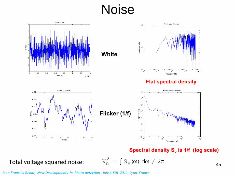
Noise
Flat spectral density
White
Flicker
(1/f)
Spectral density
Sv
is
1/f (log scale)
Total voltage squared
noise: 22 /d)(SV vn
Jean‐Francois Genat, New Developments in Photo‐detection , July 4‐8th 2011 Lyon, France

46
Equivalent Noise Charge
Jean‐Francois Genat, New Developments in Photo‐detection , July 4‐8th 2011 Lyon, France
Equivalent Noise Charge:
The charge (in electrons) that
produces
the same
rms
output as the noise of the full device
with
no input signal.
The first stage
of the electronics
chain
is
the main contributor
to the output noise
since
it
is
multiplied
by the whole
gain of the chain.
Subsequent
noise contributions are multiplied
by the product
of last gains only
47
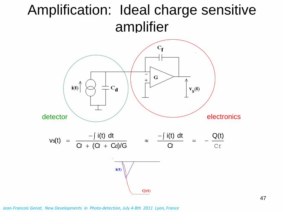
Amplification: Ideal charge sensitive amplifier
fC
Q(t)C
dti(t))/GC(CC
dti(t)(t)v
fdffs
detector electronics
Jean‐Francois Genat, New Developments in Photo‐detection, July 4‐8th 2011 Lyon, France

48
Charge sensitive amplifier Serial noise
Serial noise is
proportional
to detector capacitance:Weighted
by Cd
/Cf
f
dn
dff
dns
C
Ce)t(Q
G/)C(CC
Cedti(t)(t)v
Serial noise: preamplifierfirst stage
Jean‐Francois Genat, New Developments in Photo‐detection, July 4‐8th 2011 Lyon, France
49
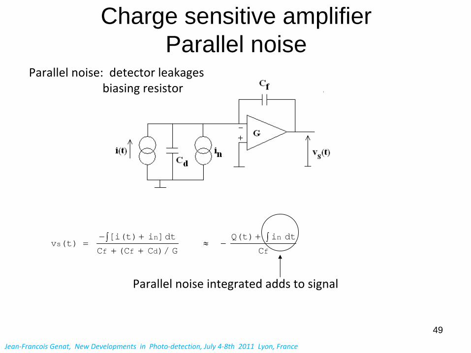
Charge sensitive amplifier Parallel noise
f
n
dff
ns
C
dtiQ(t)
G/)C(CC
dt]i[i(t)(t)v
Parallel
noise integrated
adds
to signal
Parallel
noise: detector leakagesbiasing
resistor
Jean‐Francois Genat, New Developments in Photo‐detection, July 4‐8th 2011 Lyon, France

50
Charge sensitive amplifier Total noise
2222222222fdnfnf
2dnn C/CeC/iC/]Z/ei[)(S
Serial noise flat
Noise total spectral density S():
21 /noiseParallel
Hz/V
02/d)(Srmsnoise
EfoxfAfdf/n fWLC/kIi 21
38222 /kTgZei md/nthermn
MOS transistor noises
Noise ‘corner’
Jean‐Francois Genat, New Developments in Photo‐detection, July 4‐8th 2011 Lyon, France

51
Input transistor sizingNoise is
mainly
produced
in the input stage, as it
is
multiplied
afterwards
by the gain of the other
stagesThe input transistor is
critical
MOS transistor Inversion regimes:
Strong linear : VGS > Vth
and VDS < ( VGS – Vth
)
Strong saturation: VGS > Vth: and
VDS < ( VGS – Vth
)
Weak: VGS < Vth
t
thgsdd
nVVVII
exp0
]2
)[(2
DSDSthGSoxnD
VVVVLWCI
)]2(1()[( 2satDDSthGSoxnD VVVV
LWCI
Jean‐Francois Genat, New Developments in Photo‐detection, July 4‐8th 2011 Lyon, France

52
Input transistor sizingReduce
power going
from
strong
to moderate-weak
inversion
-
Strong
inversion: gm
proportional
to W/L √Id- Cgs
proportional
to WL-
ENC proportional
to (Cdet
+ Cgs)/ √gm
-
Optimum W/L: Cgs
= 1/3 Cdet
-
Large transistors are easy
in moderate/weak
inversion at
low currents
Optimum size in weak
inversion
- gm
independent
of W, L, proportional
to Id
-
ENC minimal for Cgs
minimal, provided
thetransistor remains
in weak
inversion
MOSFETs
models
are pretty
accurate
today, even
for deep
submicron
processes
(L <100nm)
Jean‐Francois Genat, New Developments in Photo‐detection, July 4‐8th 2011 Lyon, France

53
Example: Cd(Zn)Te Xrays detectors readout
16 x 16 pixels readout
(camera of 2048 pixels / 8 cm2)
-
32-channel
front-end self triggering- RC2
shaper-
Peak
detector
-
Baseline holder
(pulses have a long tail
due to slow holes
in CdTe)-
Variable gain stage, 50, 100, 150, 200 mV/fC
-
ENC=68 e-
at
5.4 s peaking
time and 2 pF input capacitanceto achieve
1 keV
FWHM energy
resolution
at
60 keV
-
1 MeV dynamic
range-
Discriminator, DAC threshold
-
AMS 350nm-
SEL Radiation hard library
-
0.8 mW / channel
IdEFX Saclay
Jean‐Francois Genat, New Developments in Photo‐detection, July 4‐8th 2011 Lyon, France
54
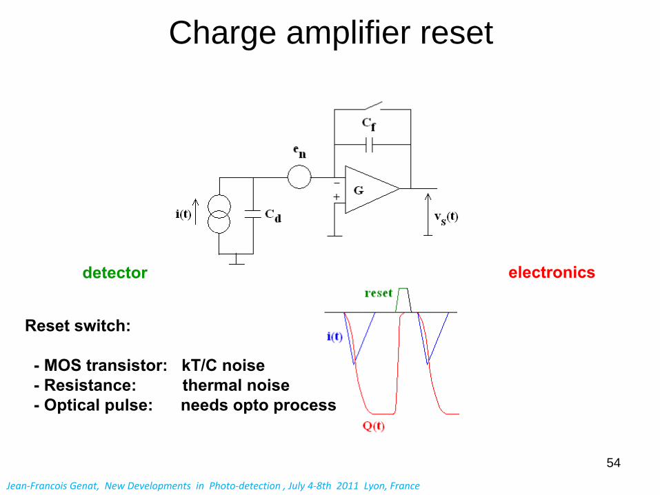
Charge amplifier reset
detector electronics
Reset switch:
-
MOS transistor: kT/C noise-
Resistance: thermal noise
-
Optical pulse: needs
opto
process
Jean‐Francois Genat, New Developments in Photo‐detection , July 4‐8th 2011 Lyon, France

55
Pulse Shaping
Analog
filtering
at
frequencies
that
optimize
signal/noiseE.g. CR RC, CR RC2
or digitize
(if speed and power allow)Digital filtering
Useful
signal spectrum
Preamplifier
noise
Jean‐Francois Genat, New Developments in Photo‐detection, July 4‐8th 2011 Lyon, France

56
ENC after CR-RCn Pulse shaping
CR: high
pass
RCn: low
pass
Limit
n is
gaussian
But higher order
filters
have drawbacks (noise…)
Series
noise in Parallel
noise in 1/f noise independent
of/1
Series
Parallel
Jean‐Francois Genat, New Developments in Photo‐detection, July 4‐8th 2011 Lyon, France
ENC vs shaping time
Waveform vs shaping time

57
ENC optimization in sub-micron CMOSExample: Charge amplifier for Avalanche Photo-Diodes
readout
Exemple of noise minimization
vs shaping
time and width
of the input transistors
= 136ns, W = 2mm
X. FANG
Jean‐Francois Genat, New Developments in Photo‐detection, July 4‐8th 2011 Lyon, France

58
Switched Integration
- Convolution with a window function (Band-pass, Sinc)
- The switch is implemented easily (instead of large resistors)
- Fast reset: no pile-up
- Needs synchronous operations
- Performance similar to CR-RCn
Jean‐Francois Genat, New Developments in Photo‐detection, July 4‐8th 2011 Lyon, France

59
Transimpedance amplifier
Jean‐Francois Genat, New Developments in Photo‐detection, July 4‐8th 2011 Lyon, France
Gain = R
High counting
rate
Typically
used
for optical
link
receivers
Easily
ringing
with
capacitive detector
Inductive input impedance
Leq
= R/ωC
Resonance at : fres= 1/2π √LeqCd
Quality
factor: Q = R / √Leq/CdQ
> 1/2 induces
ringing
Damping
with
capacitance
Easier
with
fast
amplifiers
dfs GZZ
RIV/1
)(/)( det
0
2RG
CC df
C de la Taille
60
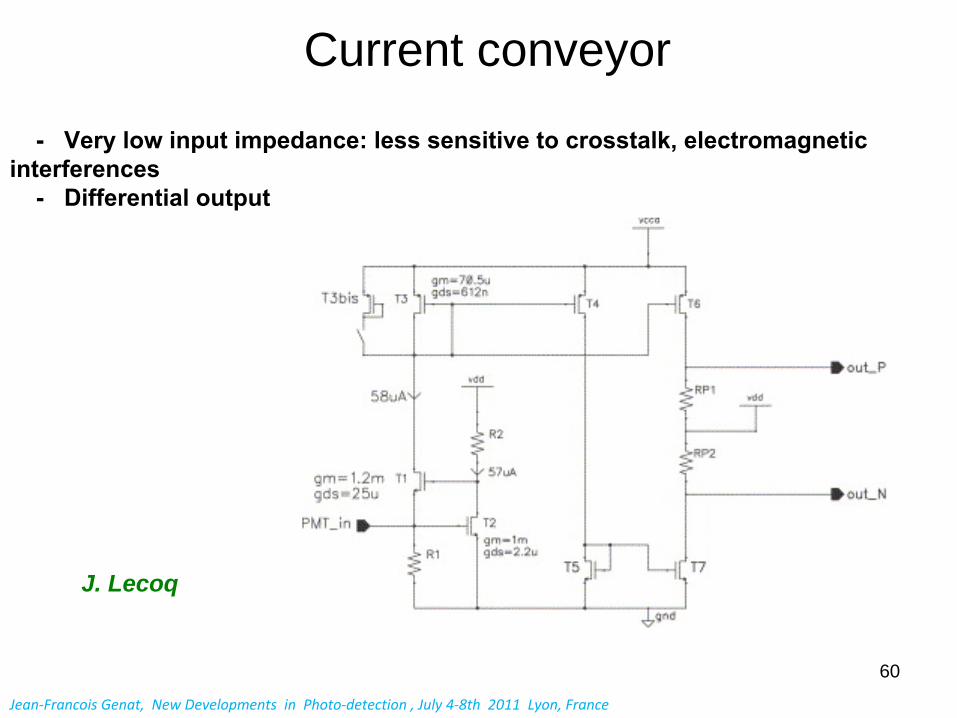
Current conveyor
-
Very
low
input impedance: less
sensitive to crosstalk, electromagnetic interferences
-
Differential
output
J. Lecoq
Jean‐Francois Genat, New Developments in Photo‐detection , July 4‐8th 2011 Lyon, France

Input impedance versus magnitude
61J. Lecoq
Jean‐Francois Genat, New Developments in Photo‐detection, July 4‐8th 2011 Lyon, France

62
Charge vs Current preamplifiers
Jean‐Francois Genat, New Developments in Photo‐detection, July 4‐8th 2011 Lyon, France
C de la Taille
Charge preamps
Best noise performanceBest with
short signals
Best with
small
capacitance detectors
Current
preamps
Best for long signalsBest for high counting rateSignificant
parallel
noise

63
Guidelines for low-noise design
Noise
-
Reduce
detector capacitance-
Avoid
as much
as possible connectors
and cables, try
to digitize
on front-end
-
Increase
the first stage gain keeping
matching
with
Cdet
-
Shape at
the optimum peaking
time
Jean‐Francois Genat, New Developments in Photo‐detection, July 4‐8th 2011 Lyon, France

64
ADCs (see J. Lecoq presentation in 2007)Ramp
ADCsConvert
to time (TDC). Compare level
to a ramp
until
trigger. Very
effective if many
channels
in parallel
(switched
capacitors
arrays)A few MHz at
more. 1 comparator/channel1 common
(Gray) counter1 ramp
generatorCan be
speeded
up using
an analog
feedback from
already
eliminated
codes
Successive approximation (SAR)Compare level
bit after
bit to bit-voltages references..Subtract
the winner bit up to LSB.Faster
by N/2N
Conversion times 1-10 MHz1 shift register1 digital to analog
converter/channel1 subtractor/channel1 comparator/channel
Flash ADCsCompare level
to all possible codings
generated
from
a voltage divider
bridgeVery
heavy, power hungry, but very
effectiveGS/s speeds
2N
comparators/channelsEncoding
logic
Pipe-line Digitize
on N-bit, subtract
DAC encoded
resultMultiply
residual
by 2 to a next
identical
stage, up to LSBN-bit ADC1 multiplication by 21 comparator
Jean‐Francois Genat, New Developments in Photo‐detection, July 4‐8th 2011 Lyon, France

65
ADCsit
fractionalPipe-line structure, with
two
thresholds/bit to manage code borders, delaying
decision
to the next
stage after
signal amplified
by 2.
Sigma-DeltaContinuously
sampling
device. One_bit
output obtained
from
comparison
between
the integral
of the previous
differences
between
level
and this
normalized
bit-output. Output oscillates
when
conversion achieved. Average
level
of the bits tream
is
proportional
to the input signal level. Low
pass
filter
recovers
the digital data in binary
format
-
Very
accurate
(>20-bit)-
Very
slow (kHz range)-
1 integrator, 1 comparator, 1-bit DAC/channel
These
ADC have replaced
ramp
ADCsBut photo-detection
needs
mainly
ramp
ADCs: high
channel
count to convert
in parallel
All ADCs need an input sample and hold device to assert a stable level during conversion
Many
hybrid
devices, depending
on the best case-dependent
trade-off between
area, power, technology
cost
e.g. SAR/flashPhoto-detectors
Very
application dependent: CCD need
parallel
operation
for column
readout, pixels can
accomodate
one low
resolution
ADC/pixel
http://www.in2p3.fr/actions/formation/microelectronique07/porquerolpdf2007.pdf
Jean‐Francois Genat, New Developments in Photo‐detection, July 4‐8th 2011 Lyon, France

66
Pulse Sampling ADCs, IPs
Trade-off precision
/ sampling
speed / power
Example:
Discrete
ADCs
on the market
24-b Dual-slope
16-bit SA + Flash 12-b 3.6GS/s8-b 56GS/s
Custom IPs: AMS 350nm 12-b 1MHz purchased
by IN2P3TSMC 130nm 14-b 150 MHz 300mW nSilition
(Belgium)SOS 90nm 12-b 220 MHz 50mW Anacatum
(Sweden)Chartered
350nm 8-b 40 MHz
NTLab
(Russia)IHP BiCMOS
250nm
14-b 25 MHz
NTLab
(Russia)IHP BiCMOS
250nm
2x 12-b 8kHz NTLab
(Russia)
TSMC 130nm 4.25 Gb/s Quad SerDes
Mixel
(USA)TSMC 28nm PLL 2-3.6GHz 1ps jitter
Silicon
Creation
(USA)Chartered
350nm
PLL 300MHz
NTLab
(Russia)
Jean‐Francois Genat, New Developments in Photo‐detection, July 4‐8th 2011 Lyon, France

67
ADCs Power
P. O’Connor
Jean‐Francois Genat, New Developments in Photo‐detection, July 4‐8th 2011 Lyon, France

68
Photo-multiplier readout
Jean‐Francois Genat, New Developments in Photo‐detection, July 4‐8th 2011 Lyon, France
64-anode MaPMT
photo-detector
16-channel
ASIC in AMS 350nmIncludes:
-
Input integrator-
8_bit ADC-
Parallel
to Serial conversionJ. Lecoq
http://www.sciencedirect.com/science/article/pii/S0168900206008886#bib3

69
CMOS 8-bit ADC ramp generator
-
Charge capacitors
at
constant current-
Cascoded
current
sources (linearity)-
Two
symetric
ramps-
5.12 s duration-
4V range-
Linearity
0.085%
J. Lecoq
Jean‐Francois Genat, New Developments in Photo‐detection, July 4‐8th 2011 Lyon, France

70
CMOS ADC latched comparator
-
Differential-
Cascoded-
Positive feedback-
300 V sensitivity
J. Lecoq
Jean‐Francois Genat, New Developments in Photo‐detection , July 4‐8th 2011 Lyon, France

71
Silicon PMT readoutAMS SiGe
350nm technology
line from
LAL Orsay
Maroc
64-channel
photon counting1/3 Photo-Electron
trigger sensitivity50fC dynamic
rangeTunable
slow channel
for chargeTunable
fast
channel
for timingInternal
8-12 ramp
ADC
Easiroc
32 inputs8-bit DAC for gain adjustmentTwo
control analog
channelsFast
trigger channels
for timingLow
power: 5mW/ch
Contact LAL Orsay: P Barrillon
http://www.omega.in2p3.fr(Need
registration)
C de la Taille
Jean‐Francois Genat, New Developments in Photo‐detection, July 4‐8th 2011 Lyon, France

Full Orsay 0.35m SiGe line
Chip Optimized
for #ch
#triggers Data type Outputs
MAROC MaPMT
64 64 Th Q
1 Q analog
+ digSPIROC SiPM
36 Th Q t
1 Q analog
Dig
EASIROC SiPM
32 32 Th Q 2 Q analogHARDROC RPC 64 Th Q
1 Q analog
Dig
MICROROC MicroMegas 64 Th Q
1 Q analog
Dig
SKIROC PIN diodes 64 Th Q
1 Q analog
DigPARISROC PMTs
Matrix
16 16 Th Q t Dig
SPACIROC MaPMT
64 64 Th Q
9 Q
http://www.omega.in2p3.fr
Jean‐Francois Genat, New Developments in Photo‐detection , July 4‐8th 2011 Lyon, France
73
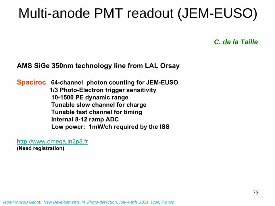
Multi-anode PMT readout (JEM-EUSO)
AMS SiGe
350nm technology
line from
LAL Orsay
Spaciroc
64-channel
photon counting
for JEM-EUSO1/3 Photo-Electron
trigger sensitivity10-1500 PE dynamic
rangeTunable
slow channel
for chargeTunable
fast
channel
for timingInternal
8-12 ramp
ADCLow
power: 1mW/ch
required
by the ISS
http://www.omega.in2p3.fr(Need
registration)
C. de la Taille
Jean‐Francois Genat, New Developments in Photo‐detection, July 4‐8th 2011 Lyon, France

7474
Fast Switched Capacitors Arrays (SCA)-
Fast
photo-detectors as Micro-Channel Plates or Silicon
Photo-Multipliers
signals
analysed
on-chip as with
digital oscilloscopes
-
Regular
PMTs
sampled
to 13-bit dynamic
range (E. Delagnes, D. Breton)
Principle of SCA ASICs:
Write
fast
(1-10GS/s)Read as possible (10-100 MHz)Digitize
all caps in parallel
with
a ramp
ADC
Input discriminator
as trigger to stop sampling
Key component of digital scopes
Examples:
DRS4 S. Ritt
(PSI) 6GS/s 850 MHz 250nmSAM D. Breton, E. Delagnes
(France)
3GS/s 300 MHz 350nmLAB G Varner
(Hawaii)
6GS/s 900 MHz 250nmPSEC H Grabas, E. Oberla
(Chicago) 15GS/s 600 MHz 130nm
Limitations:
Random
noiseSample
aperture jitterSampling
timebase
jitter
Jean‐Francois Genat, New Developments in Photo‐detection, July 4‐8th 2011 Lyon, France

7575
SCAs
Main features:
- Sampling frequency- Analog bandwidth - Analog dynamic range (ADC bits)- Depth- Readout frequency
Capacitors bank
Timing generator
Analog input
A/D converterTrigger
Jean‐Francois Genat, New Developments in Photo‐detection, July 4‐8th 2011 Lyon, France
7676
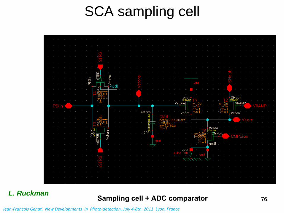
SCA sampling cell
Sampling
cell
+ ADC comparatorL. Ruckman
Jean‐Francois Genat, New Developments in Photo‐detection, July 4‐8th 2011 Lyon, France
7777
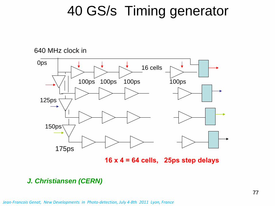
40 GS/s Timing generator
100ps 100ps 100ps 100ps
125ps
150ps
16 cells
16 x 4 = 64 cells, 25ps step delays
640 MHz clock in
175ps
0ps
J. Christiansen (CERN)
Jean‐Francois Genat, New Developments in Photo‐detection, July 4‐8th 2011 Lyon, France
7878
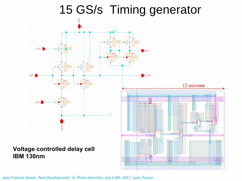
15 GS/s Timing generator
Voltage controlled
delay
cellIBM 130nm
Jean‐Francois Genat, New Developments in Photo‐detection, July 4‐8th 2011 Lyon, France
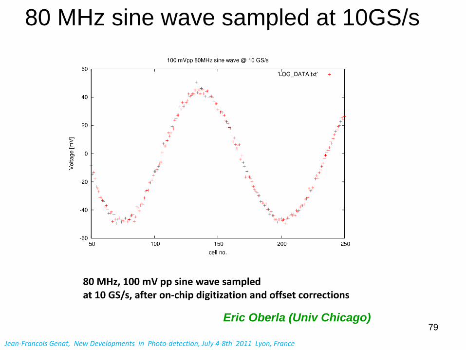
79
80 MHz, 100 mV pp sine wave sampled at 10 GS/s, after on‐chip digitization and offset corrections
mV
Units of 100ps
Eric Oberla (Univ Chicago)
80 MHz sine wave sampled at 10GS/s
Jean‐Francois Genat, New Developments in Photo‐detection, July 4‐8th 2011 Lyon, France

80
Sampled DC value before and after offsets subtraction Offsets due to voltage threshold spreads (fixed pattern)
Eric Oberla (Univ Chicago)
SCA Offsets distribution
Jean‐Francois Genat, New Developments in Photo‐detection, July 4‐8th 2011 Lyon, France

81
VME board equipped with SCA chips
Jean‐Francois Genat, New Developments in Photo‐detection, July 4‐8th 2011 Lyon, France
D. Breton, E. Delagnes

- Introduction
- Contexts
-
High Energy
Physics-
Space, Medical
- Photodetectors
- Vacuum-
Solid
state
- Photodetectors
Electronics
-
Components-
Technologies-
Photon counting-
Amplitude, charge-
Imaging-
Timing-
3D integration
-
Conclusion
Jean‐Francois Genat, New Developments in Photo‐detection, July 4‐8th 2011 Lyon, France

83
Charge Coupled
Devices
(CCD)Set of electrodes
on top of high
resistivity
silicon, top or backside
illuminatedScientific
CCDs: huge
dynamic
range (16-bit), single electron
sensitivity
if cooled.
Pixels are readout serially with fast amplifiers (one per electrodes array)Charge shifts horizontally into vertical registers which are readout serially.
-
Transfer from
cell
to cell
is
noiseless, 99.999%… efficiency-
Charge is
transfered
from
the last pixel to a voltage follower
(floating
gate)after
reseting
the node. The node
is
sensed
before
and after
transfer
Correlated
Double Sampling
(CDS, eliminates
reset noise)
Jean‐Francois Genat, New Developments in Photo‐detection, July 4‐8th 2011 Lyon, France

84
Off-chip amplification, noiseless
transfer
CCD to readout
chip
On readout
chip capacitive transimpedance
amplifier after
on-CCD CDShttp://www.fairchildimaging.com/main/documents/CCD_CMOS_Hybrid_FPA_for_Low_Light_Level_Imaging.pdf
Fairchild
CCDs
readout
Noise before
CDS
Jean‐Francois Genat, New Developments in Photo‐detection, July 4‐8th 2011 Lyon, France
Amplifier transfer
function
CDS transfer
function

85
CCD readout-
Most CCD noise is system noise after CDS-
Cooled at -100˚C (173K), dark current is negligible-
Charge transfer efficiency almost perfect (i.e. 1 ppm
charge diffusion)-
Companion (bi)CMOS
ASIC needed for amplification, ADC, clock generation
CCD readout ASICs:
- ASPIC (LPNHE Paris) for the Large Synoptic Survey Telescope(LSST) focal plane at 173K. 350 CMOS.-
> 16-bit dynamic range, noise < 7 V rms-
Correlated Double Sampling
-
CRIC (LBNL) for SuperNovae
Acceleration Probe / Joint Dark Energy Mission(SNAP/JDEM). Space boarded telescope at 140K, 10 kRad
tolerance. 250nm CMOS.-
Correlated Double Sampling-
> On-chip pipe-line ADC (13-bit), -
noise < 6.8 V rms
-
Sidecar (Teledyne) -
Up to 16 Mpixel
support-
36 analog channels, Correlated Double Sampling-
16-bit ADC 100 kHz-
12-bit AC 10 MHz-
CCD clock signals generation: kHz-MHz, 10-20V clocks
http://www.teledyne-si.com/imaging/sidecar.html
Jean‐Francois Genat, New Developments in Photo‐detection, July 4‐8th 2011 Lyon, France

86
Monolithic
Active Pixel Sensors
(MAPS)
Pixels instrumented
with
amplifier and switches
Sensitive volume is
a silicon
epitaxial
layer
surrounded
by a reverse biased
collecting
PN junction
3‐transistor structure 4‐transistor structure
4‐T isolates
pixel and multiplexer
structures allowing
using
CDS
IEEE Trans
Nucl
Sci
Vol 57 n5 Oct 2010, p2490-2496
M. Tyndel, R. Turchetta et al.
C. de la Taille
Amplifying
structure
Resets
at
column
voltage
R. Kaufmann, CSEM
Jean‐Francois Genat, New Developments in Photo‐detection, July 4‐8th 2011 Lyon, France
87
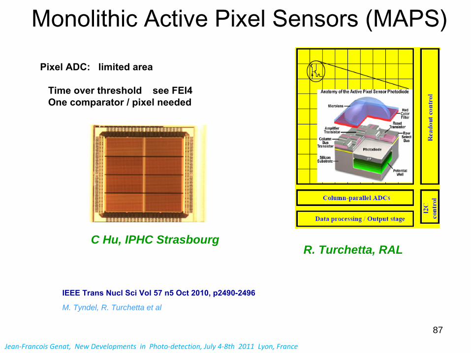
Monolithic
Active Pixel Sensors
(MAPS)
Pixel ADC: limited
area
Time over threshold
see
FEI4 One comparator
/ pixel needed
IEEE Trans
Nucl
Sci
Vol 57 n5 Oct 2010, p2490-2496
M. Tyndel, R. Turchetta et al
R. Turchetta, RALC Hu, IPHC Strasbourg
Jean‐Francois Genat, New Developments in Photo‐detection, July 4‐8th 2011 Lyon, France

88
Monolithic
Active Pixel Sensors
(MAPS)
-
Mimosa line
IPHC Strasbourg
Jean‐Francois Genat, New Developments in Photo‐detection, July 4‐8th 2011 Lyon, France
89
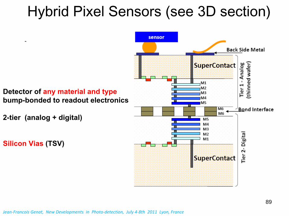
Hybrid
Pixel Sensors
(see
3D section)
-
Jean‐Francois Genat, New Developments in Photo‐detection, July 4‐8th 2011 Lyon, France
Detector of any
material
and typebump-bonded
to readout
electronics
2-tier
(analog
+ digital)
Silicon
Vias
(TSV)

90
DEPFET readout CMOS 180nm
90
DEPFET: modulate the drain current of a MOSFET with ionisationcreated on the gate (MPI, Gemany)
Jean‐Francois Genat, New Developments in Photo‐detection, July 4‐8th 2011 Lyon, France
J. Knopf

- Introduction
- Contexts
-
High Energy
Physics-
Space, Medical
- Photodetectors
- Vacuum-
Solid
state
- Photodetectors
Electronics
-
Components-
Technologies, -
Photon counting-
Amplitude, charge-
Imaging-
Timing-
3D integration
-
Conclusion
Jean‐Francois Genat, New Developments in Photo‐detection, July 4‐8th 2011 Lyon, France
92
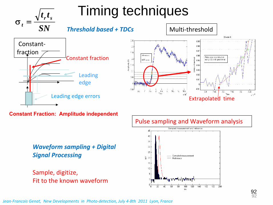
Timing techniques
Extrapolated time
Multi‐threshold
Leading edge errors
Leadingedge
Constant fraction
Constant‐
fraction
Pulse sampling and Waveform analysis
Sample, digitize,Fit to the known waveform
Threshold based + TDCs
Waveform sampling + DigitalSignal Processing
92
Constant Fraction: Amplitude independent
Jean‐Francois Genat, New Developments in Photo‐detection, July 4‐8th 2011 Lyon, France
SNtt sr
t

93
Methods compared (simulation)
Time resolution vs
Number of photo-electrons
zoom
Jean‐Francois Genat, New Developments in Photo‐detection, July 4‐8th 2011 Lyon, France

Time to Digital Conversion
Many
custom ASICs
based
on analog
or digital techniques
Analog
-
Ramp
between
Tstart
and Tstop-
Digitize
level
with
an ADC, or ramp
down slow and count
10ps resolution
possible
Digital
-
Count clock
for coarse
time (<100MHz)-
Interpolate
with
vernier digital delay
lines
locked
on clock
10ps resolution
possible
Hybrids
!
Jean‐Francois Genat, New Developments in Photo‐detection, July 4‐8th 2011 Lyon, France

HPTDC (CERN)• 32 channels(100ps binning)
or 8 channels (25ps binning)• LVDS (differential) or LVTTL (single ended) inputs• 40MHz time reference (LHC clock)• Leading, trailing edge and time over threshold (for leading edge
time corrections)
• Non triggered• Triggered with programmable latency, window and overlapping triggers• Buffering: 4 per channel, 256 per group of 8 channels, 256 readout fifo• Token based readout with parallel, byte-wise or serial interface• JTAG control, monitoring and test interface• SEU error detection.• Power consumption: 0.5W –
1.5W depending on operating mode.INL RC mode
-5-4-3-2-1012345
1 101 201 301 401 501 601 701 801 901 1001
binJ. Christiansen CERN
Jean‐Francois Genat, New Developments in Photo‐detection, July 4‐8th 2011 Lyon, France
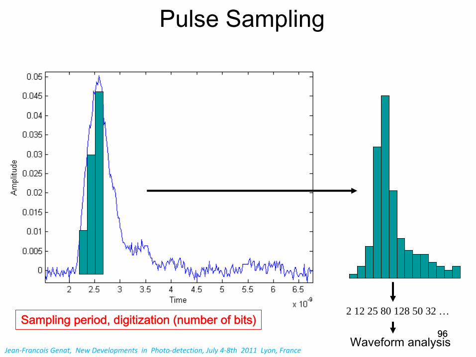
9696
2 12 25 80 128 50 32 …Sampling period, digitization (number of bits)
Waveform analysis
Pulse Sampling
Jean‐Francois Genat, New Developments in Photo‐detection, July 4‐8th 2011 Lyon, France

97
Pulse SamplingADC: Number
of bits
Quantization
noise is
LSB/Signal noise should
be
significantly
more than
Q noiseXmax
Largest
signal of interest
:
Sample
rate 1/
1/
above
twice
the Shannon-Nyquist
frequency: the highest
frequency
above
noiseNOT the 3dB cut-off:
12
)LSB/X(LogN maxbit 2
Jean‐Francois Genat, New Developments in Photo‐detection, July 4‐8th 2011 Lyon, France

98
Example: PSEC3 6-channel Sampling ASIC specifications
10 GS/s sampling ASIC for Micro-Channel Plates Readout
Maximum sampling rate 15GS/sAnalog Bandwidth 2 GHzDynamic range 0.8VNumber of channels 6Number of cells
256Sampling window adjustable 500ps-2nsADC Resolution 8-bit (12-bit implemented)Crosstalk 1%DC Input impedance 50
internal (channels 0 and 1)50
internal (channels 2 and 3)Clock
40 MHzConversion clock 1-2 GHz internal ring oscillator Readout time 4 x 256 x 25ns=25.6 msPower 40mW/channel @ 1.2VProcess IBM 8RF-DM (130nm CMOS)
Input analog bus laid out as a 50
transmission line
Jean‐Francois Genat, New Developments in Photo‐detection, July 4‐8th 2011 Lyon, France
99
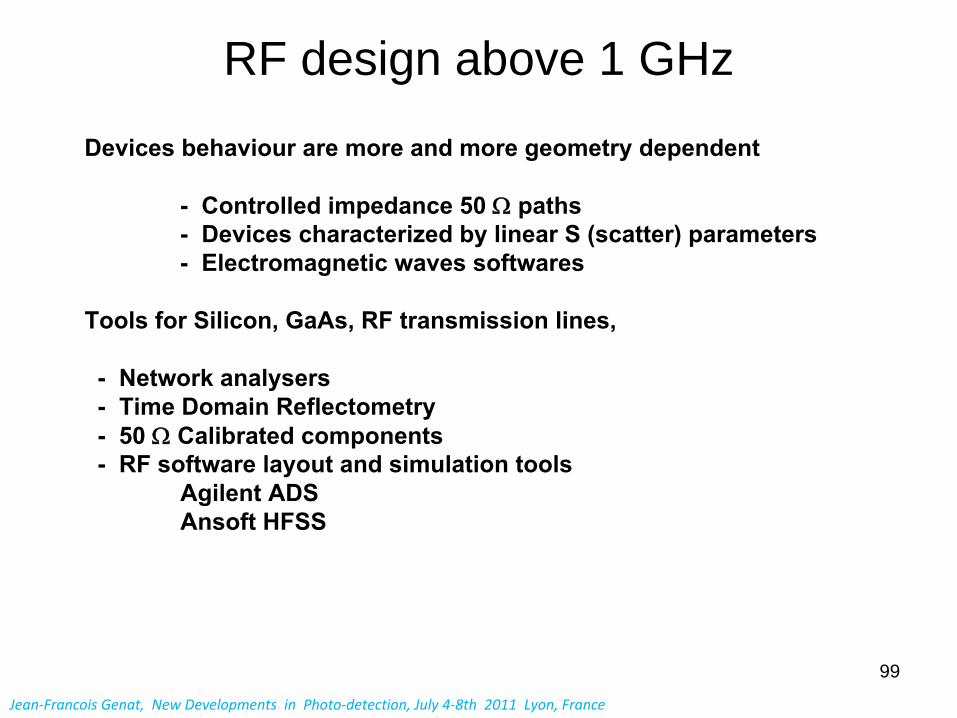
RF design above 1 GHz
Devices
behaviour
are more and more geometry
dependent
-
Controlled
impedance
50
paths-
Devices
characterized
by linear
S (scatter) parameters
-
Electromagnetic
waves
softwares
Tools for Silicon, GaAs, RF transmission lines,
-
Network analysers-
Time Domain Reflectometry
-
50
Calibrated
components-
RF software layout
and simulation tools
Agilent
ADSAnsoft
HFSS
Jean‐Francois Genat, New Developments in Photo‐detection, July 4‐8th 2011 Lyon, France

100
RF designDC-10 GHz simulations of a large area (20 x 20 cm) Micro-Channel Plate based
detector using
Ansoft
HFSS electromagnetic
simulator
Simulation shows that
device
is functional
up to 2.3 GHz at
15dB
Transmission line implementedon glass for 2D Micro-Channel plate readout
H. Grabas
Jean‐Francois Genat, New Developments in Photo‐detection, July 4‐8th 2011 Lyon, France
15dB

101
Processing
of digital sampled
data
Determine
which
information is
useful
in the waveform: Rising
edge, integral, maximum amplitude.
For photo-detectors, usually
time and charge
(integral
of the current
pulse)
Pulse shaping
can
be
done
in digital if power and speed allow
(ADC)Jean‐Francois Genat, New Developments in Photo‐detection, July 4‐8th 2011 Lyon, France

102
Original MCP measured
signal Signal
template
(obtained
by averaging100 signals
to remove
noise)
Example: Least squares algorithm:
Minimize
to get
accurate
time and maximum amplitude
N
i)xx( itempimeas
1
22
Fast
timing: Processing
of sampled
data
Jean‐Francois Genat, New Developments in Photo‐detection, July 4‐8th 2011 Lyon, France

103
,dx/,dt/ max 0202 0
N
itempmeas )xx( ii
1
22
22ii temp
itemp 'x.xb
Obtain
t0
and xmax:
:
t0
xmax
0202
1
202
maxii x/t/,)xx( ,
N
itempmeas
i
temp i'xbp 2 bp.abd 2
22ii temp
imeas x.xmp 22
ii tempi
meas 'x.x'mp
)d/b.mpd/a.'mp(t/x)bp.mpb'mp(d/t max. 00 11
Example: find
pulse time and maximum amplitude
i
temp ixa 2
Solve:
Processing
of digital sampled
data
Jean‐Francois Genat, New Developments in Photo‐detection, July 4‐8th 2011 Lyon, France

104
Digital filteringSignal as a sequence
of numbers, compute
weighted
sums
with
a Digital Signal Processor.
-
Finite
Impulse Response: convolution with
the sampled
impulse response-
Infinite
Impulse Response: recursive, use of the z-domain
frequency
response:
Example: 1st order
RC filter)RC/texp(C)t(y
/RCa
)z)a()a(
z)z(Q/)z(P 1
1
111
RCj)j(H
11
1
1
112
z
z/j
jj
ii
zb
za)z(Q/)z(P
)k(xxk(yy k),k
]xxy)a[(a
y )k()k()k()k( 1111
1
Digital
Analog
Digitalrecursive
Analog
j
jkjj
jkjk xbyay
mmm
nnn
jb
ja)j(Q/)j(P
Jean‐Francois Genat, New Developments in Photo‐detection, July 4‐8th 2011 Lyon, France

105
Digital filteringExample: 1st order
RC filter
RCj)j(H
11
)RC/texp(C)t(y
)z)a()a(
z)z(H 1
1
111
Analog
Digitalrecursive
]xxy)a[(a
y )k()k()k()k( 1111
1
Jean‐Francois Genat, New Developments in Photo‐detection , July 4‐8th 2011 Lyon, France

106
Pico-second timing and 2D position for large area detectors with delay lines
• Delay lines readout and pulse sampling provide
-
Fast timing (2-10ps)-
One dimension with delay lines readout 100mm-
1mmTransverse dimension can be obtained from centroids
Less electronics channels for large area sensors
t1
, a1 t2
, a2
½
(t1
+ t2
) = timev(t1
‐t2
) = longitudinal position i
ai
/
i
= transverse position
Pico‐second electronicsPico‐second electronics
106
Timing extration
with sampling andDigital Signal Processing3.8 ps
translates in 190 m position resolution wiith
50 photo-electrons5 x 5 cm
MCP
Jean‐Francois Genat, New Developments in Photo‐detection, July 4‐8th 2011 Lyon, France
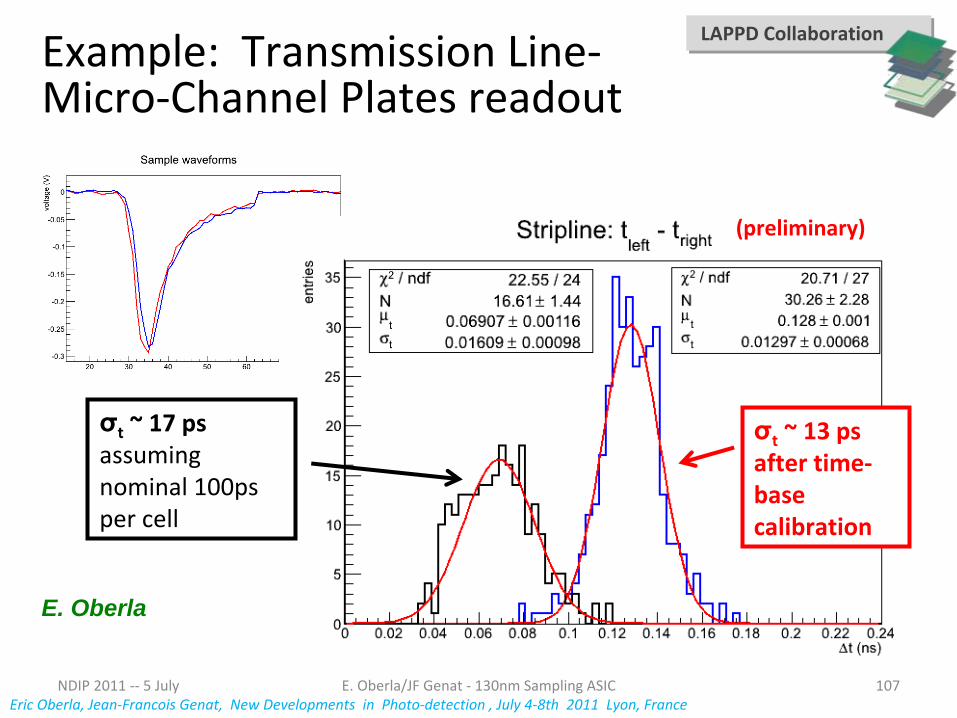
NDIP 2011 ‐‐
5 July
Example: Transmission Line‐ Micro‐Channel Plates readout
LAPPD Collaboration LAPPD Collaboration
σt
~ 17 ps assuming nominal 100ps
per cell
σt
~ 13 ps after time‐ base
calibration
(preliminary)
107E. Oberla/JF Genat
‐
130nm Sampling ASICEric Oberla, Jean‐Francois Genat, New Developments in Photo‐detection , July 4‐8th 2011 Lyon, France
E. Oberla

- Introduction
- Contexts
-
High Energy
Physics-
Space, Medical
- Photodetectors
- Vacuum-
Solid
state
- Photodetectors
Electronics
-
Components-
Technologies, -
Photon counting-
Amplitude, charge-
Imaging-
Timing-
3D integration
-
Conclusion
Jean‐Francois Genat, New Developments in Photo‐detection, July 4‐8th 2011 Lyon, France

109
3D IntegrationGoal: increase the integration density
Interconnections: Two
options: die to die
-1 Stack
up several
layers
of different
IC processes
Interconnections. Through
Silicon
Vias
(TSV) if more than
2 layers
Die can
be
tested
-2 2D in a thinner
process
Limit
of CMOS (10nm) is
coming
soon, option 1 will
be
mandatoryIn addition, thin
processes
are always expensive. But 3D could
be
as well…
3D tools
emerging:-
Simulation-
Layout-
Extraction
http://cmp.imag.fr/Spl-Session_3DIC/02_CMP.pdf
2-tier
2-tier
w/TSV Multi-tier
hybrid
w/TSV
K. Torki
Jean‐Francois Genat, New Developments in Photo‐detection, July 4‐8th 2011 Lyon, France

Piet De Moor (IMEC), TWEPP 2010Jean‐Francois Genat, New Developments in Photo‐detection, July 4‐8th 2011 Lyon, France
3D Imagers

111
3D Integration
-
Shorter
connectionsLower
impedance
Less
RC delaysSave power
-
Higher
densityBetter
heat
Smaller
I/O pitch
Area x Timing x Power =Factor 15
Wafer bonding
for 3D integrationCu on SiO2
interconnect
structuresJ.J Lu
Jean‐Francois Genat, New Developments in Photo‐detection , July 4‐8th 2011 Lyon, France

112
Applications
- Memories, Memory on CPU
IBM, Samsung
-
Pixellated
photo-detectors:
-
Optics
microlenses, filters, -
Pixels Photo-Detector,
-
Electronics
(analog
+ digital),-
Serial opto
out
MIT Lincoln Labs, RTI, Ziptronix
Key feature:
Through
Silicon
Via (TSV)
Jean‐Francois Genat, New Developments in Photo‐detection, July 4‐8th 2011 Lyon, France

113
2-tier 3D process tools- PDK:
from
CMC +
TSVs
from
Tezzaron
- Libraries:
Core
+ I/O from
ARM
-
Memory compiler:
S/DPRAM and ROM from
ARM
-3 D Utilities:
Contributions developments
-Tutorial, User’s
setup
Intallation
easy
-
Support of Cadence CDB and OpenAccess
databases K. Torki
Jean‐Francois Genat, New Developments in Photo‐detection, July 4‐8th 2011 Lyon, France
114
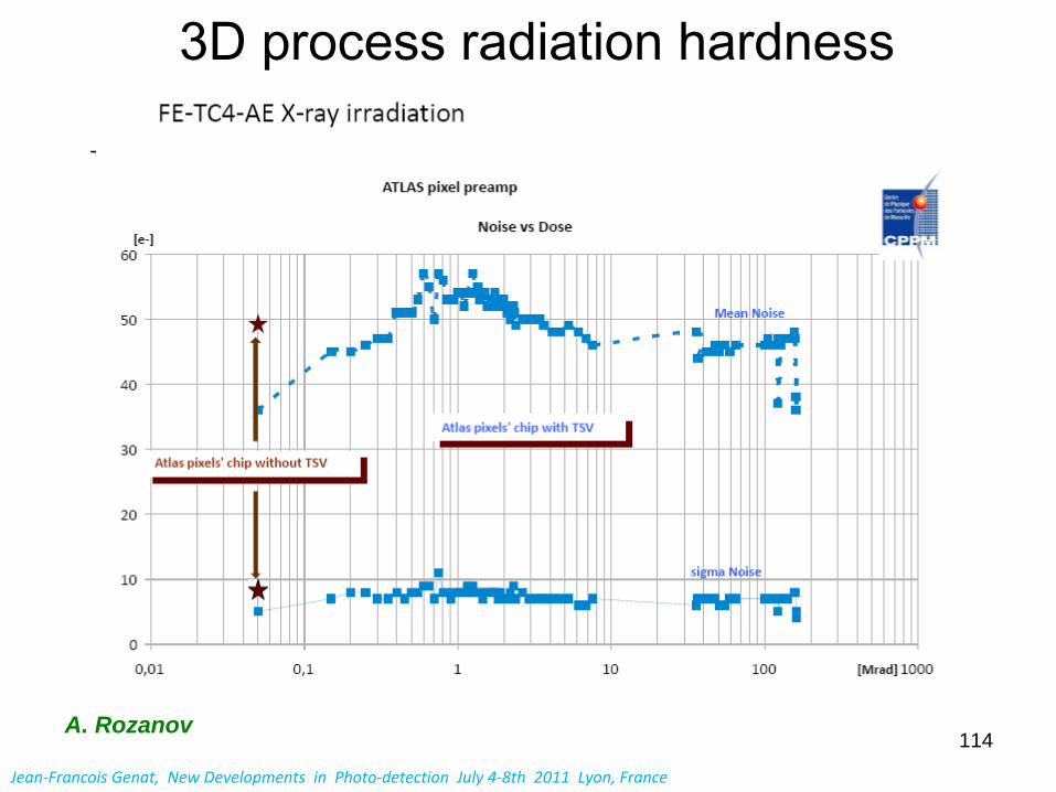
3D process
radiation hardness
-
Jean‐Francois Genat, New Developments in Photo‐detection July 4‐8th 2011 Lyon, France
K. Meier
A. Rozanov
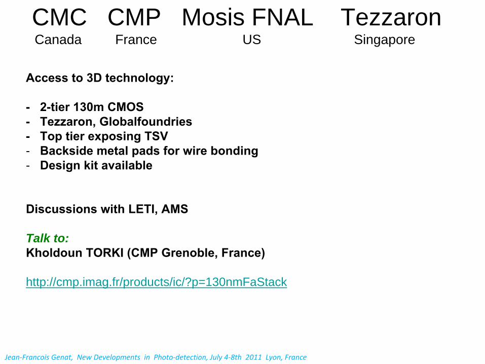
CMC CMP Mosis FNAL Tezzaron Canada France US Singapore
Access to 3D technology:
-
2-tier
130m CMOS -
Tezzaron, Globalfoundries
-
Top tier
exposing
TSV- Backside
metal
pads for wire
bonding
- Design kit available
Discussions with
LETI, AMS
Talk to:Kholdoun
TORKI (CMP Grenoble, France)
http://cmp.imag.fr/products/ic/?p=130nmFaStack
Jean‐Francois Genat, New Developments in Photo‐detection, July 4‐8th 2011 Lyon, France

1st MPW run
Fermilab
Top tier
Bottom
tierJean‐Francois Genat, New Developments in Photo‐detection, July 4‐8th 2011 Lyon, France

3D Integration CMP/MOSIS/CMC 1st MPW run
MPW run May 31st, 2011Jean‐Francois Genat, New Developments in Photo‐detection, July 4‐8th 2011 Lyon, France
K.Torki
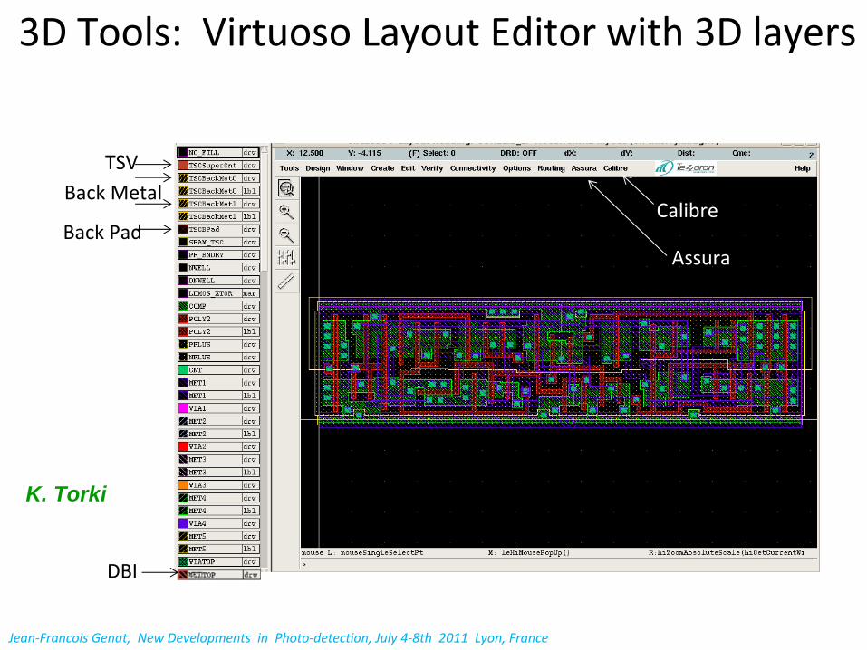
3D Tools: Virtuoso Layout Editor with 3D layers
TSVBack Metal
Back Pad
DBI
Assura
Calibre
K. Torki
Jean‐Francois Genat, New Developments in Photo‐detection, July 4‐8th 2011 Lyon, France

Jean‐Francois Genat, New Developments in Photo‐detection, July 4‐8th 2011 Lyon, France
Tools for Tezzaron
MicroMagix MAX 3D
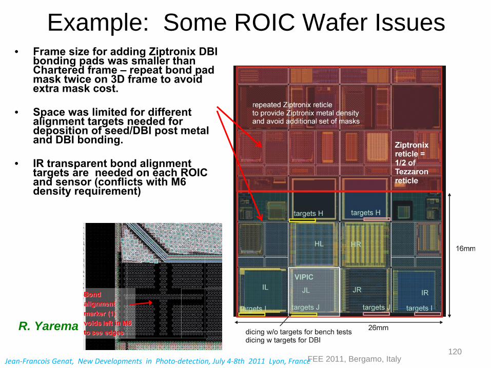
• Frame size for adding Ziptronix
DBI bonding pads was smaller than Chartered frame –
repeat bond pad mask twice on 3D frame to avoid extra mask cost.
• Space was limited for different alignment targets needed for deposition of seed/DBI post metal and DBI bonding.
• IR transparent bond alignment targets are needed on each ROIC and sensor (conflicts with M6 density requirement)
120FEE 2011, Bergamo, Italy
Example: Some ROIC Wafer Issues
R. Yarema
Jean‐Francois Genat, New Developments in Photo‐detection, July 4‐8th 2011 Lyon, France
121
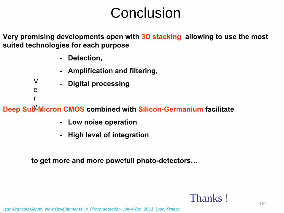
Conclusion
Jean‐Francois Genat, New Developments in Photo‐detection, July 4‐8th 2011 Lyon, France
V e r y
Very
promising
developments
open with
3D stacking
allowing
to use the most suited
technologies for each
purpose
-
Detection,
-
Amplification and filtering,
-
Digital processing
Deep
Sub-Micron CMOS
combined
with
Silicon-Germanium
facilitate
-
Low
noise operation
-
High level
of integration
to get
more and more powefull
photo-detectors…
Thanks !

122Jean‐Francois Genat, New Developments in Photo‐detection, July 4‐8th 2011 Lyon, France

123
Extra slides
Jean‐Francois Genat, New Developments in Photo‐detection, July 4‐8th 2011 Lyon, France
124
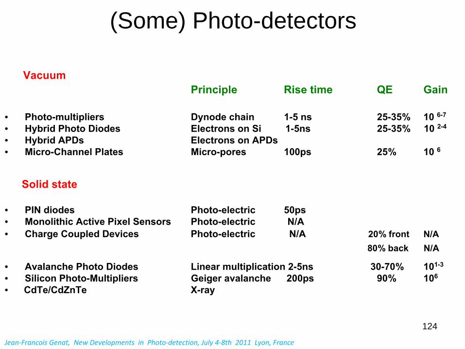
(Some) Photo-detectors
VacuumPrinciple
Rise time
QE
Gain
• Photo-multipliers
Dynode chain
1-5 ns
25-35%
10 6-7
• Hybrid
Photo Diodes
Electrons on Si 1-5ns
25-35% 10 2-4
• Hybrid
APDs
Electrons on APDs• Micro-Channel Plates
Micro-pores
100ps
25%
10 6
Solid
state
• PIN diodes
Photo-electric
50ps• Monolithic
Active Pixel Sensors
Photo-electric
N/A • Charge Coupled
Devices
Photo-electric
N/A 20% front N/A80% back N/A
• Avalanche Photo Diodes Linear
multiplication 2-5ns
30-70%
101-3
• Silicon
Photo-Multipliers
Geiger avalanche
200ps
90%
106
• CdTe/CdZnTe
X-ray
Jean‐Francois Genat, New Developments in Photo‐detection, July 4‐8th 2011 Lyon, France
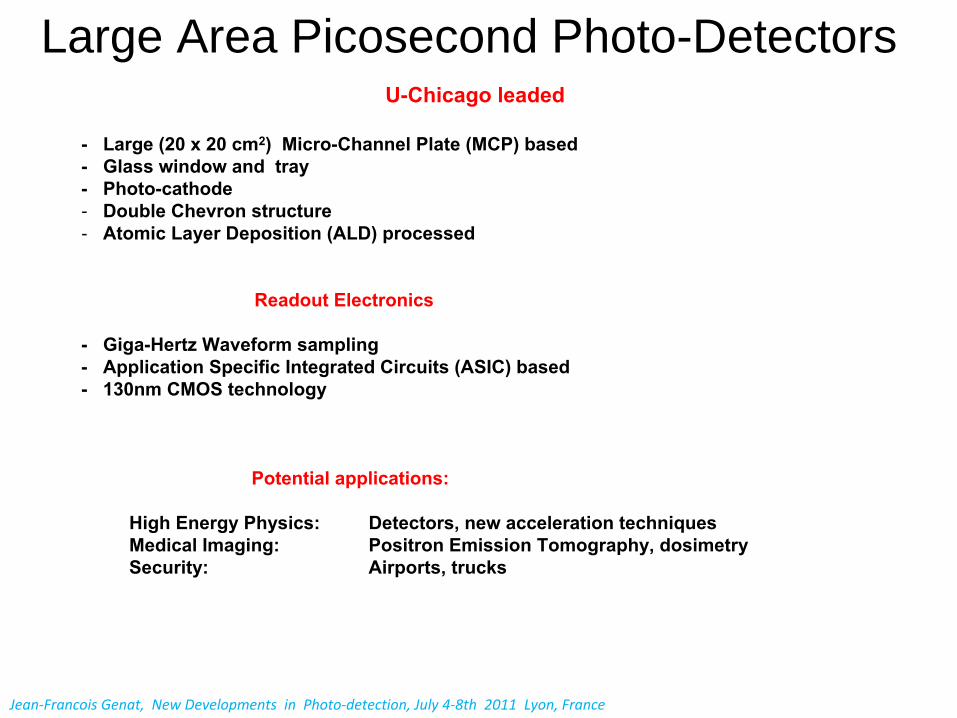
Large Area Picosecond Photo-DetectorsU-Chicago leaded
-
Large (20 x 20 cm2) Micro-Channel Plate (MCP) based-
Glass window
and tray-
Photo-cathode- Double Chevron structure- Atomic
Layer Deposition
(ALD) processed
Readout
Electronics
-
Giga-Hertz
Waveform
sampling-
Application Specific
Integrated
Circuits (ASIC) based-
130nm CMOS technology
Potential
applications:
High Energy
Physics: Detectors, new acceleration
techniquesMedical
Imaging: Positron Emission Tomography, dosimetrySecurity: Airports, trucks
Jean‐Francois Genat, New Developments in Photo‐detection, July 4‐8th 2011 Lyon, France

126
Signal simple Spice model
nstnst
)/texp()/texp()t(y
10251
21
Spice
detector model: difference
of two
exponentials
Jean‐Francois Genat, New Developments in Photo‐detection, July 4‐8th 2011 Lyon, France
127
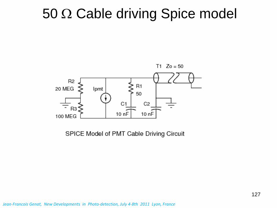
50
Cable driving Spice model
Jean‐Francois Genat, New Developments in Photo‐detection, July 4‐8th 2011 Lyon, France

128128
Micro-Channel Plate Detectors
Pore diameter 3-25 mPore aspect ratio: 1:50
1st
gap
pores
2d gap
a few mm
200 V
1-
2kV
200 V
Anodes (1.6 x 1.6mm2 pixels)
Photo-cathode
Jean‐Francois Genat, New Developments in Photo‐detection, July 4‐8th 2011 Lyon, France
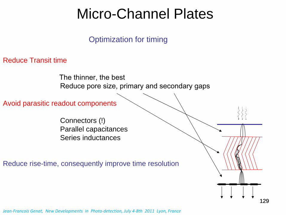
129129
Micro-Channel Plates
Reduce Transit time
The thinner, the bestReduce pore size, primary and secondary gaps
Avoid parasitic readout components
Connectors (!)Parallel capacitancesSeries inductances
Reduce rise-time, consequently improve time resolution
Optimization for timing
Jean‐Francois Genat, New Developments in Photo‐detection, July 4‐8th 2011 Lyon, France

130130
Imaging Micro-Channel Plates DetectorsAs imaging device…
Coupling to Ceramic
Coupling to BoardPosition: 10m resolutionTime: 1ns
From J. Lapington, for WSO, Uni. Leicester, UK
Coupling to ASIC:
3 m
From GLAST, Siegmund et alNIM 591 2008
Jean‐Francois Genat, New Developments in Photo‐detection, July 4‐8th 2011 Lyon, France

131131
Two-micron space resolution using analog charge division technique
High precision analog measurements.
But integration time= 200ns !
Jean‐Francois Genat, New Developments in Photo‐detection, July 4‐8th 2011 Lyon, France

132132
Micro-channel Plates Sampled Waveforms
- Amplitudes (10m, 2.5 kV)
18 Photo-Electrons 20 mV 50 Photo-Electrons 35 mV
158 Photo-Electrons 78 mV
- Rise times
25m 600ps10m 550ps
Jean‐Francois Genat, New Developments in Photo‐detection, July 4‐8th 2011 Lyon, France
133133
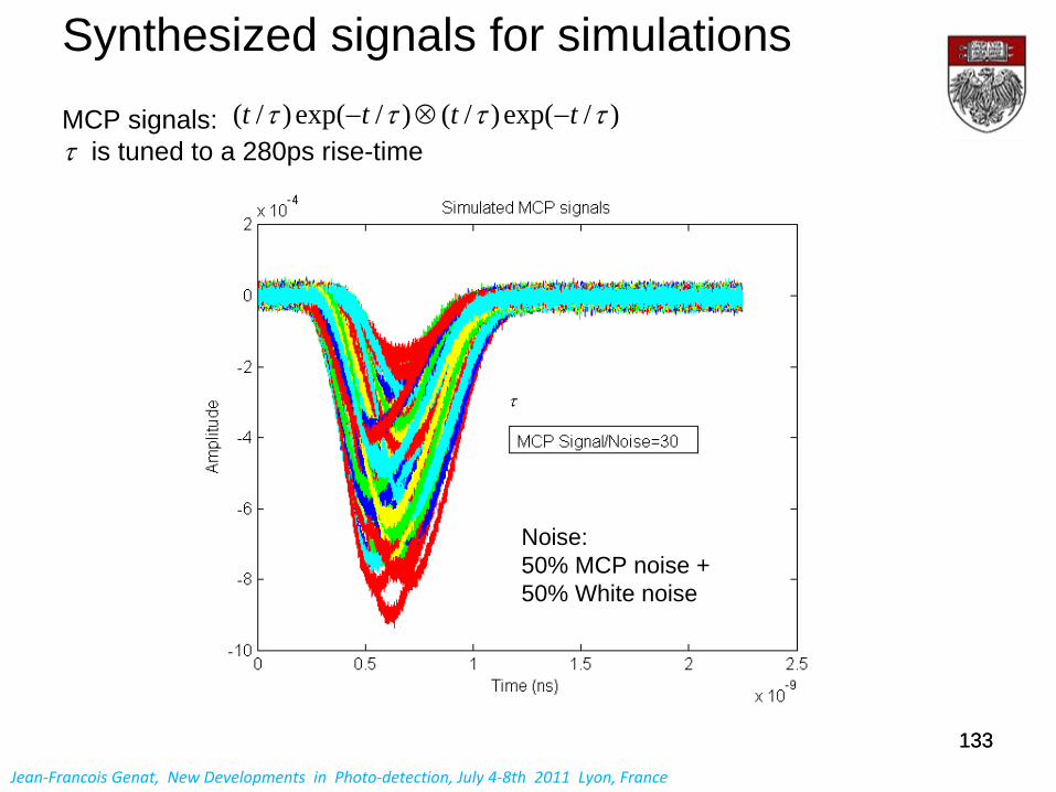
MCP signals: is tuned to a 280ps rise-time
)/exp()/()/exp()/( tttt
Synthesized signals for simulations
Noise:50% MCP noise +50% White noise
Jean‐Francois Genat, New Developments in Photo‐detection, July 4‐8th 2011 Lyon, France

134134
MCP Signals spectra
Same noise corner at 1.2 GHz
Measured (FNAL T979 Beam-Tests) Simulated
2x2mm2 1”x 1”
MCP signalWhite noiseMCP noiseTotal
Jean‐Francois Genat, New Developments in Photo‐detection, July 4‐8th 2011 Lyon, France

135135
Single Threshold: Noise and Slope
dttdx
xt)(/
Single threshold: Time spread proportional to amplitude noise and inverse to slope
X(t)
-
-
xnoiserms
t
Jean‐Francois Genat, New Developments in Photo‐detection, July 4‐8th 2011 Lyon, France

136136
Pulse sampling and Waveform analysis
- Sampling frequency: Set at twice the largest frequency in the signal spectrum
f0 2f0
- Digitization: Evaluate what is needed from signals properties:
Example:
MCP signals
Jean‐Francois Genat, New Developments in Photo‐detection, July 4‐8th 2011 Lyon, France
137137
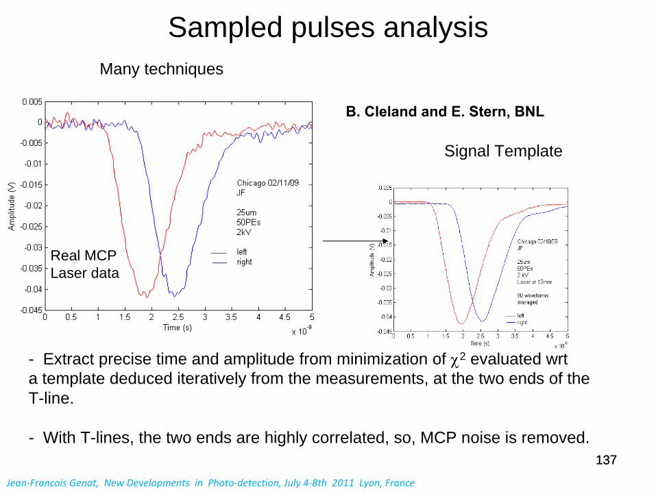
Sampled pulses analysis
- Extract precise time and amplitude from minimization of 2 evaluated wrta template deduced iteratively from the measurements, at the two ends of theT-line.
- With T-lines, the two ends are highly correlated, so, MCP noise is removed.
Real MCP Laser data
Signal Template
Many techniques
B. Cleland and E. Stern, BNL
Jean‐Francois Genat, New Developments in Photo‐detection, July 4‐8th 2011 Lyon, France

138138
Iterative template
Template from average Template iterativestd= 4.26ps std=3.93
At T-lines ends
Jean‐Francois Genat, New Developments in Photo‐detection, July 4‐8th 2011 Lyon, France

139139
Pulse sampling Timing resolution vs Sampling rate (simulation)
Timing resolution vs Sampling rate / Analog bandwidth
Jean‐Francois Genat, New Developments in Photo‐detection, July 4‐8th 2011 Lyon, France

140140
Pulse sampling benefits
Pulse sampling and waveform analysis:
• Picosecond timing with fast detectors• Charge: centroids for 2D readout
• Resolve double pulse
For large area detectors read with delay lines in series
Jean‐Francois Genat, New Developments in Photo‐detection, July 4‐8th 2011 Lyon, France
141141
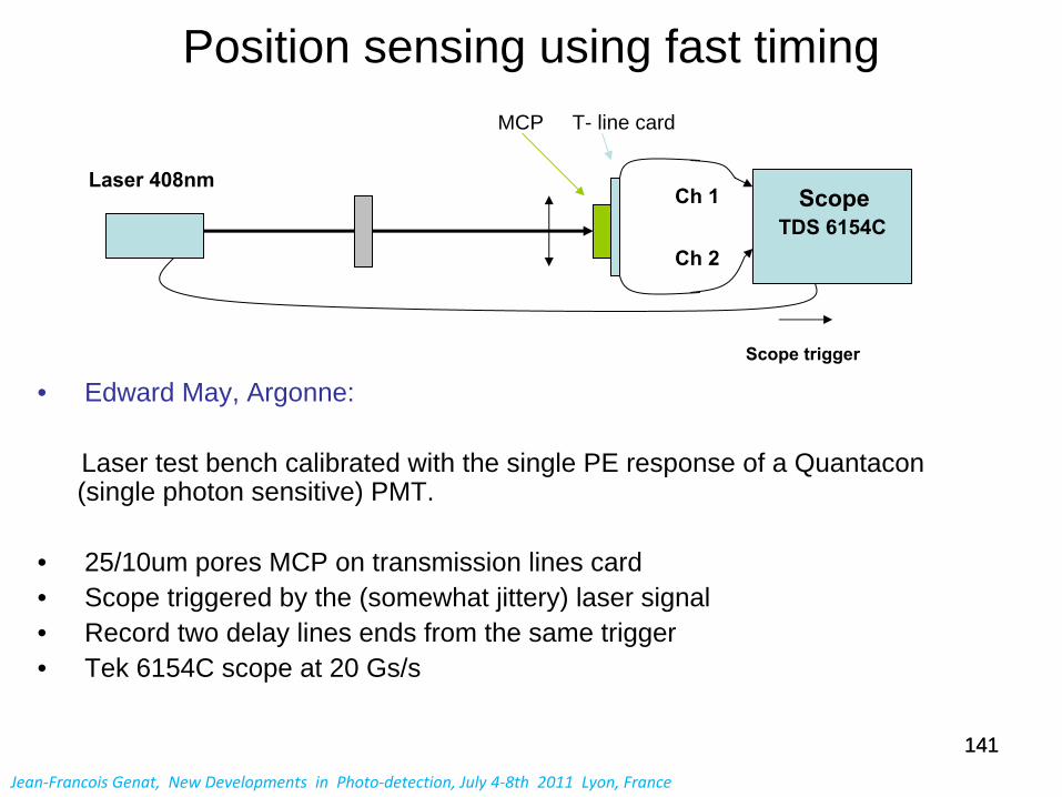
Position sensing using fast timing
• Edward May, Argonne:
Laser test bench calibrated with the single PE response of a Quantacon (single photon sensitive) PMT.
• 25/10um pores MCP on transmission lines card• Scope triggered by the (somewhat jittery) laser signal• Record two delay lines ends from the same trigger• Tek 6154C scope at 20 Gs/s
TDS 6154C
Scope trigger
Ch 1
Ch 2
MCP T- line card
Laser 408nmScope
Jean‐Francois Genat, New Developments in Photo‐detection, July 4‐8th 2011 Lyon, France

142142
Results
Position resolution (velocity=8.25ps/mm) : 50PEs 4.26ps 213m158PEs 1.95ps 97m
Jean‐Francois Genat, New Developments in Photo‐detection, July 4‐8th 2011 Lyon, France

143143
Measurements vs simulation
50PEs rms=3.82ps vs 2.5ps (simulation)
18PEs rms = 6.05ps vs 7ps (simulation)
Measurementsdo not match exactly since MCP noiseis partly removed (T-lines ends correlated)
Jean‐Francois Genat, New Developments in Photo‐detection, July 4‐8th 2011 Lyon, France

144144
Position Resolution at 158PEs
158 PEs
HV = 2.3 kV HV = 2.4 kV 2.5 kV 2.6 kVStd 12.8ps 2.8ps 2.2 ps
1.95 ps
640m 140m 110m 97m
Jean‐Francois Genat, New Developments in Photo‐detection, July 4‐8th 2011 Lyon, France

145145
Transmission lines as anodes
• Present Photonis MCPs:Pixellated anodes, pitch of 1.6 x 1.6 mm
- Atomic Layer Deposition (ALD) detectors- Waveform sampling with fast sampling chips
• Integration of lines as anodes in vacuum for large area sensors• Plates of 1”
x 1”
in ALD process • Modules of 8 “
x 8 “
?• One vacuum vessel (glass)
1”1”
glass
ALD micro-channel plate
Henry Frisch, (U-Chicago)W. Hau, M. Pellin (ANL)
Check in vacuum T-lines coupled to Micro-Channel Plates (impedance, velocity)
B. Adams, K Attenkoffer, ANL
Jean‐Francois Genat, New Developments in Photo‐detection, July 4‐8th 2011 Lyon, France

146146
MCPs: Best position resolution
O. Siegmund, A. Tremsin (SSL Berkeley)
A few microns position resolution using analog weighted sums
Jean‐Francois Genat, New Developments in Photo‐detection, July 4‐8th 2011 Lyon, France
147
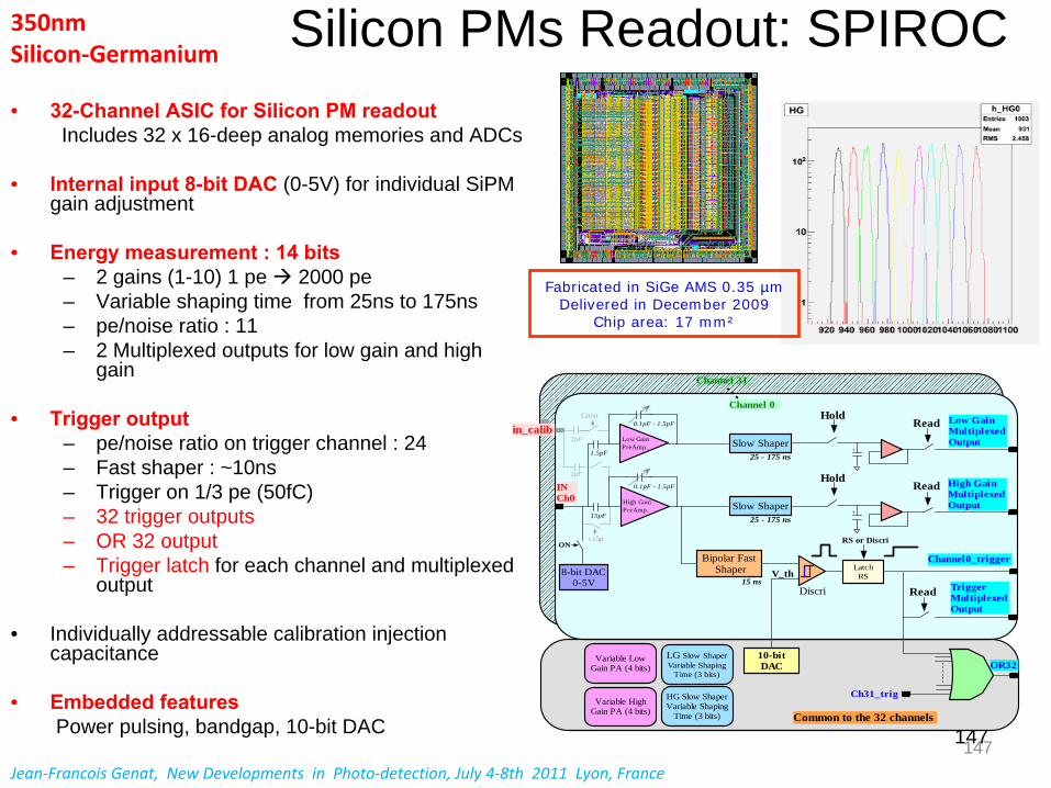
Silicon PMs Readout: SPIROC• 32-Channel ASIC for Silicon PM readout
Includes 32 x 16-deep analog memories and ADCs
• Internal input 8-bit DAC
(0-5V) for individual SiPM gain adjustment
• Energy measurement : 14 bits– 2 gains (1-10) 1 pe 2000 pe– Variable shaping time from 25ns to 175ns – pe/noise ratio : 11– 2 Multiplexed outputs for low gain and high
gain
• Trigger output– pe/noise ratio on trigger channel : 24– Fast shaper : ~10ns– Trigger on 1/3 pe (50fC)– 32 trigger outputs– OR 32 output– Trigger latch for each channel and multiplexed
output
• Individually addressable calibration injection capacitance
• Embedded featuresPower pulsing, bandgap, 10-bit DAC
Fabricated in SiGe AMS 0.35 µm Delivered in December 2009
Chip area: 17 mm²
350nm Silicon‐Germanium
147
Variable LowGain PA (4 bits)
HoldRead
Low GainMultiplexedOutput
Ch31_trig
Channel 0
Common to the 32 channels
Channel 31
Variable HighGain PA (4 bits)
+
V_thLatch
RS
Channel0_trigger
Discri
OR32
Slow Shaper25 - 175 ns
LG Slow ShaperVariable Shaping
Time (3 bits)
15 nsRead Trigger
MultiplexedOutput
Low GainPreAmp.
HG Slow ShaperVariable Shaping
Time (3 bits)
0.1pF - 1.5pF
1.5pF
10-bitDAC
RS or Discri
0.1pF - 1.5pF
15pF
High GainPreAmp.
HoldRead
High GainMultiplexedOutput
+Slow Shaper25 - 175 ns
2pF
Ctest
2pF
in_calib
Bipolar Fast Shaper8-bit DAC
0-5V
INCh0
ONc15p
Jean‐Francois Genat, New Developments in Photo‐detection, July 4‐8th 2011 Lyon, France

148
Switched Capacitor Arrays (SCA)
15 GS/s 130nm CMOS
- Sampling
capacitors: 50-100 fF, input bus 200-1k- Analog
bandwidth
= 1/2RC = 1-10GHz- Dynamic
range 10-13 bits limited
by noise and voltage droop
before
readout- Timing generator
using
voltage controlled
delay
elements
of 50-500ps- Depth
can
be
very
large (64k) if bandwidth
is
not constrained- Very
low
power (readout
dominated)
- Used
in fast
oscilloscopes
Jean‐Francois Genat, New Developments in Photo‐detection, July 4‐8th 2011 Lyon, France