journal of materials chemistry c -...
TRANSCRIPT
This journal is©The Royal Society of Chemistry 2016 J. Mater. Chem. C, 2016, 4, 3915--3933 | 3915
Cite this: J.Mater. Chem. C, 2016,
4, 3915
Polymorphism as an emerging design strategy forhigh performance organic electronics
Hyunjoong Chung and Ying Diao*
Organic electronics is a promising field spanning a wide range of applications, with unrivaled advantages
in low production cost, versatility in material synthesis, and compatibility with a wide range of substrates
including flexible polymeric materials. Organic molecules are characterized by weak van der Waals
interactions, which grant access to multiple crystalline packing states (crystal polymorphism) at near
ambient conditions. Different polymorphs, even with the slightest changes in their molecular packing can
have electronic properties that differ by orders of magnitude. Therefore, accessing metastable polymorphs
can serve as a novel design strategy for attaining high device performance. Recently, this strategy has
been successfully applied to small organic molecules such as 6,13-bis(triisopropylsilylethynyl)pentacene
(TIPS-pentacene) and 2,7-dioctyl[1]benzothieno[3,2-b][1]benzothiophene (C8-BTBT) and high hole mobilities
have been attained in organic field-effect transistors fabricated using their metastable structures. In addition,
polymorphism serves as an excellent platform for advancing the fundamental understanding of charge
transport in p-conjugated systems. The relationship between molecular packing and charge transport
can be unequivocally established since the chemical structures are identical amongst polymorphs,
leaving molecular packing as the only variable in the case of packing polymorphism.
1. Introduction1.1 The rise of organic electronics
The field of organic electronics, also known as organic and largearea electronics (OLAE), has attracted much attention from theresearch community and the industry, fueled by its advantagesand versatility for a variety of applications including biochemicalsensors, radio frequency identification (RFID) tags, smartphonedisplays, flexible light sources, portable solar cells, and curvedtelevision screens.1–10 One of the major advantages of organicelectronics is their solution processability, enabling low-cost,large-area deposition on flexible substrates.11 Another advantageis that chemical synthesis can be utilized to fine-tune manyproperties of organic semiconductors, some of which are solubilityin organic solvents, electronic structures, and chemical stability.Thanks to rapid materials innovation in the last thirty years, wehave witnessed improvement in charge carrier mobility oforganic semiconductors of over six orders of magnitude, withthe highest hole mobility on par with polycrystalline silicon andmetal-oxide transistors.12 The door is wide open for organicelectronics to extend the current capabilities of the traditionalsilicon electronics.
Although organic semiconductors were identified as early asin the 1940s, extensive studies on them began later in the 1960s
by Martin Pope and colleagues13 on their study of the electronicstructure of anthracene. After the discovery of metallic con-ductivity in p-conjugated complexes of tetrathiafulvalene I andtetracyanoquinodimethane II,14 more research ensued with theidea that small organic molecules would be a major playerfor the next generation of electronics.2,11,13,15–17 The organicfield-effect transistor (OFET), which is an essential buildingblock for organic circuits and also the platform for fundamentalstudy of charge transport in p-conjugated systems, soon becamea main focus in the field of organic electronics.18
Studies on organic thin-film transistors emerged in the late1980s on conjugated polymers and small molecules. In 1996,Bao and colleagues19 demonstrated the first solution printedhigh performance (40.01 cm2 V�1 s�1) plastic transistor, basedon regioregular poly(3-alkylthiophene) (P3HT). After more than25 years of continued research with a focus on improvingthe charge carrier mobility,15 the hole mobilities of thin filmtransistors well exceed those of benchmark thin-film amorphoussilicon devices17 that range from 0.5–1 cm2 V�1 s�1.
1.2 Role of polymorphism
Charge transport in small molecule semiconductors is highlysensitive to intermolecular p orbital overlap. Any slight changesin molecular packing that alter the p orbital overlap can result invariations in charge transport. In organic semiconductors, thedominant interactions are van der Waals and weak electrostatic(i.e. quadrupole) interactions, which are non-specific compared
Chemical & Biomolecular Engineering, University of Illinois at Urbana-Champaign,
600 S. Mathews Ave., Urbana, Illinois, USA. E-mail: [email protected]
Received 25th December 2015,Accepted 26th February 2016
DOI: 10.1039/c5tc04390e
www.rsc.org/MaterialsC
Journal ofMaterials Chemistry C
REVIEW
Publ
ishe
d on
29
Febr
uary
201
6. D
ownl
oade
d by
Uni
vers
idad
e Fe
dera
l de
Sant
a C
atar
ina
(UFS
C)
on 2
7/05
/201
6 20
:32:
21. View Article Online
View Journal | View Issue
3916 | J. Mater. Chem. C, 2016, 4, 3915--3933 This journal is©The Royal Society of Chemistry 2016
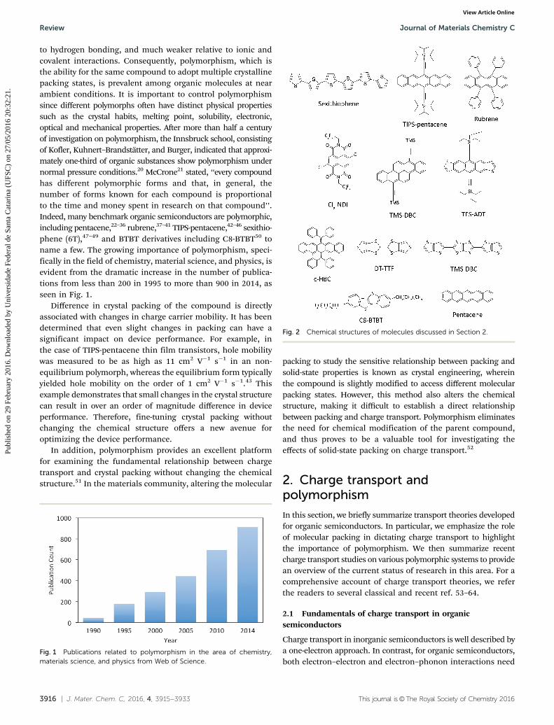
to hydrogen bonding, and much weaker relative to ionic andcovalent interactions. Consequently, polymorphism, which isthe ability for the same compound to adopt multiple crystallinepacking states, is prevalent among organic molecules at nearambient conditions. It is important to control polymorphismsince different polymorphs often have distinct physical propertiessuch as the crystal habits, melting point, solubility, electronic,optical and mechanical properties. After more than half a centuryof investigation on polymorphism, the Innsbruck school, consistingof Kofler, Kuhnert–Brandstatter, and Burger, indicated that approxi-mately one-third of organic substances show polymorphism undernormal pressure conditions.20 McCrone21 stated, ‘‘every compoundhas different polymorphic forms and that, in general, thenumber of forms known for each compound is proportionalto the time and money spent in research on that compound’’.Indeed, many benchmark organic semiconductors are polymorphic,including pentacene,22–36 rubrene,37–41 TIPS-pentacene,42–46 sexithio-phene (6T),47–49 and BTBT derivatives including C8-BTBT50 toname a few. The growing importance of polymorphism, speci-fically in the field of chemistry, material science, and physics, isevident from the dramatic increase in the number of publica-tions from less than 200 in 1995 to more than 900 in 2014, asseen in Fig. 1.
Difference in crystal packing of the compound is directlyassociated with changes in charge carrier mobility. It has beendetermined that even slight changes in packing can have asignificant impact on device performance. For example, inthe case of TIPS-pentacene thin film transistors, hole mobilitywas measured to be as high as 11 cm2 V�1 s�1 in an non-equilibrium polymorph, whereas the equilibrium form typicallyyielded hole mobility on the order of 1 cm2 V�1 s�1.43 Thisexample demonstrates that small changes in the crystal structurecan result in over an order of magnitude difference in deviceperformance. Therefore, fine-tuning crystal packing withoutchanging the chemical structure offers a new avenue foroptimizing the device performance.
In addition, polymorphism provides an excellent platformfor examining the fundamental relationship between chargetransport and crystal packing without changing the chemicalstructure.51 In the materials community, altering the molecular
packing to study the sensitive relationship between packing andsolid-state properties is known as crystal engineering, whereinthe compound is slightly modified to access different molecularpacking states. However, this method also alters the chemicalstructure, making it difficult to establish a direct relationshipbetween packing and charge transport. Polymorphism eliminatesthe need for chemical modification of the parent compound,and thus proves to be a valuable tool for investigating theeffects of solid-state packing on charge transport.52
2. Charge transport andpolymorphism
In this section, we briefly summarize transport theories developedfor organic semiconductors. In particular, we emphasize the roleof molecular packing in dictating charge transport to highlightthe importance of polymorphism. We then summarize recentcharge transport studies on various polymorphic systems to providean overview of the current status of research in this area. For acomprehensive account of charge transport theories, we referthe readers to several classical and recent ref. 53–64.
2.1 Fundamentals of charge transport in organicsemiconductors
Charge transport in inorganic semiconductors is well described bya one-electron approach. In contrast, for organic semiconductors,both electron–electron and electron–phonon interactions need
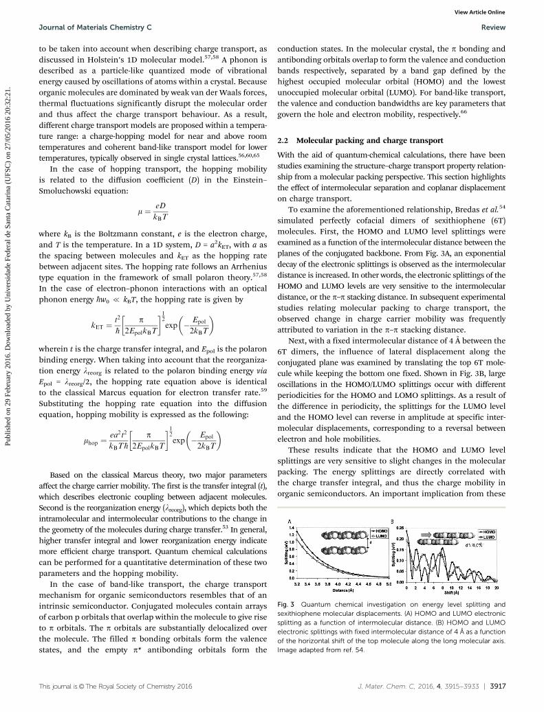
Fig. 1 Publications related to polymorphism in the area of chemistry,materials science, and physics from Web of Science.
Fig. 2 Chemical structures of molecules discussed in Section 2.
Review Journal of Materials Chemistry C
Publ
ishe
d on
29
Febr
uary
201
6. D
ownl
oade
d by
Uni
vers
idad
e Fe
dera
l de
Sant
a C
atar
ina
(UFS
C)
on 2
7/05
/201
6 20
:32:
21.
View Article Online
This journal is©The Royal Society of Chemistry 2016 J. Mater. Chem. C, 2016, 4, 3915--3933 | 3917
to be taken into account when describing charge transport, asdiscussed in Holstein’s 1D molecular model.57,58 A phonon isdescribed as a particle-like quantized mode of vibrationalenergy caused by oscillations of atoms within a crystal. Becauseorganic molecules are dominated by weak van der Waals forces,thermal fluctuations significantly disrupt the molecular orderand thus affect the charge transport behaviour. As a result,different charge transport models are proposed within a tempera-ture range: a charge-hopping model for near and above roomtemperatures and coherent band-like transport model for lowertemperatures, typically observed in single crystal lattices.56,60,65
In the case of hopping transport, the hopping mobilityis related to the diffusion coefficient (D) in the Einstein–Smoluchowski equation:
m ¼ eD
kBT
where kB is the Boltzmann constant, e is the electron charge,and T is the temperature. In a 1D system, D = a2kET, with a asthe spacing between molecules and kET as the hopping ratebetween adjacent sites. The hopping rate follows an Arrheniustype equation in the framework of small polaron theory.57,58
In the case of electron–phonon interactions with an opticalphonon energy �hw0 { kBT, the hopping rate is given by
kET ¼t2
�h
p2EpolkBT
� �12exp � Epol
2kBT
� �
wherein t is the charge transfer integral, and Epol is the polaronbinding energy. When taking into account that the reorganiza-tion energy lreorg is related to the polaron binding energy viaEpol = lreorg/2, the hopping rate equation above is identicalto the classical Marcus equation for electron transfer rate.59
Substituting the hopping rate equation into the diffusionequation, hopping mobility is expressed as the following:
mhop ¼ea2t2
kBT�h
p2EpolkBT
� �12exp � Epol
2kBT
� �
Based on the classical Marcus theory, two major parametersaffect the charge carrier mobility. The first is the transfer integral (t),which describes electronic coupling between adjacent molecules.Second is the reorganization energy (lreorg), which depicts both theintramolecular and intermolecular contributions to the change inthe geometry of the molecules during charge transfer.53 In general,higher transfer integral and lower reorganization energy indicatemore efficient charge transport. Quantum chemical calculationscan be performed for a quantitative determination of these twoparameters and the hopping mobility.
In the case of band-like transport, the charge transportmechanism for organic semiconductors resembles that of anintrinsic semiconductor. Conjugated molecules contain arraysof carbon p orbitals that overlap within the molecule to give riseto p orbitals. The p orbitals are substantially delocalized overthe molecule. The filled p bonding orbitals form the valencestates, and the empty p* antibonding orbitals form the
conduction states. In the molecular crystal, the p bonding andantibonding orbitals overlap to form the valence and conductionbands respectively, separated by a band gap defined by thehighest occupied molecular orbital (HOMO) and the lowestunoccupied molecular orbital (LUMO). For band-like transport,the valence and conduction bandwidths are key parameters thatgovern the hole and electron mobility, respectively.66
2.2 Molecular packing and charge transport
With the aid of quantum-chemical calculations, there have beenstudies examining the structure–charge transport property relation-ship from a molecular packing perspective. This section highlightsthe effect of intermolecular separation and coplanar displacementon charge transport.
To examine the aforementioned relationship, Bredas et al.54
simulated perfectly cofacial dimers of sexithiophene (6T)molecules. First, the HOMO and LUMO level splittings wereexamined as a function of the intermolecular distance between theplanes of the conjugated backbone. From Fig. 3A, an exponentialdecay of the electronic splittings is observed as the intermoleculardistance is increased. In other words, the electronic splittings of theHOMO and LUMO levels are very sensitive to the intermoleculardistance, or the p–p stacking distance. In subsequent experimentalstudies relating molecular packing to charge transport, theobserved change in charge carrier mobility was frequentlyattributed to variation in the p–p stacking distance.
Next, with a fixed intermolecular distance of 4 Å between the6T dimers, the influence of lateral displacement along theconjugated plane was examined by translating the top 6T mole-cule while keeping the bottom one fixed. Shown in Fig. 3B, largeoscillations in the HOMO/LUMO splittings occur with differentperiodicities for the HOMO and LOMO splittings. As a result ofthe difference in periodicity, the splittings for the LUMO leveland the HOMO level can reverse in amplitude at specific inter-molecular displacements, corresponding to a reversal betweenelectron and hole mobilities.
These results indicate that the HOMO and LUMO levelsplittings are very sensitive to slight changes in the molecularpacking. The energy splittings are directly correlated withthe charge transfer integral, and thus the charge mobility inorganic semiconductors. An important implication from these
Fig. 3 Quantum chemical investigation on energy level splitting andsexithiophene molecular displacements. (A) HOMO and LUMO electronicsplitting as a function of intermolecular distance. (B) HOMO and LUMOelectronic splittings with fixed intermolecular distance of 4 Å as a functionof the horizontal shift of the top molecule along the long molecular axis.Image adapted from ref. 54.
Journal of Materials Chemistry C Review
Publ
ishe
d on
29
Febr
uary
201
6. D
ownl
oade
d by
Uni
vers
idad
e Fe
dera
l de
Sant
a C
atar
ina
(UFS
C)
on 2
7/05
/201
6 20
:32:
21.
View Article Online
3918 | J. Mater. Chem. C, 2016, 4, 3915--3933 This journal is©The Royal Society of Chemistry 2016
results is that polymorphism can potentially modulate electro-nic properties of conjugated molecules over a wide range byintroducing even small changes in molecular packing. Estab-lishing the relationship between polymorphism and chargetransport can provide an effective strategy for enhancing chargetransport in organic semiconductors.
2.3 Charge transport studies on polymorphs
Bernstein pointed to the importance of polymorphism forstudying charge transport given that the only variable amongpolymorphs is the crystal structure, not chemistry or chemicalcompositions.67 Thus for a polymorphic system, electronic prop-erty differences observed can be directly related to the structuraldifferences. In the context of organic electronics, polymorphismobserved in the thin film geometry is of great interest, given thedirect relevance to charge transport in thin film field-effecttransistor devices. In such devices, charge transport frequentlyoccurs within a few molecular layers near the dielectric surface,wherein the molecular packing is often found to differ fromthe bulk phase. Interfacial phases adopting unique molecularpacking are also known as substrate induced phases (SIP).68
SIP is a polymorphic form that occurs only in the vicinity of arigid substrate and not observed among polymorphs of bulkcrystals. The formation mechanism of these polymorphs is stillunder debate.
The terms ‘‘thin film phases’’ or ‘‘thin film polymorphs’’frequently appearing in recent literature are loosely defined, as theyoften refer to polymorphs discovered in the thin film geometry. Infact, polymorphs found in thin films can either be a SIP or a bulkpolymorph kinetically favoured in the thin film geometry. Thestructural information of SIPs are significant as charge transport isinfluenced mostly by the crystal packing in the vicinity of theinterface.69 However, obtaining full structure solutions of SIPs aremuch more challenging as conventional single crystal or powderX-ray diffraction methods cannot be applied. Instead, a combinationof grazing incidence X-ray diffraction, surface-enhanced Ramanspectroscopy and computational approaches have been used toobtain the structural information of SIPs.
In this section, we summarize polymorphs of some of themost studied small molecule semiconductors and their corres-ponding electronic properties, to help examine the relationshipbetween charge transport and molecular packing. Substrateinduced phases have been found for some of the systemssummarized here. Most studies present their findings in a similarflow of steps, beginning with preparing different polymorphsthrough various methods, which will be summarized in Section 3,followed by solving the structures of crystal polymorphs throughsingle-crystal or thin-film X-ray diffraction. Then device measure-ments are performed on either single crystal or thin film field-effecttransistors of the polymorphs to quantify charge carrier mobilities.With structural data, charge transfer integrals can be calculatedbased on density functional theory. The charge carrier mobi-lities or charge transfer integrals are then compared amongdifferent polymorphs.
Major challenges exist for establishing polymorphic structure–electronic property relationship, and they are to obtain phase-pure
polymorphs, acquire complete structural information, andfabricate transistor devices from metastable polymorphs. As aresult, there are limited examples for which both polymorphicstructures and electronic properties are available. The smallmolecule semiconductors we focus on here are not necessarilythe highest performing molecules, but those with well-characterizedstructural phase spaces and corresponding charge transportmeasurements.
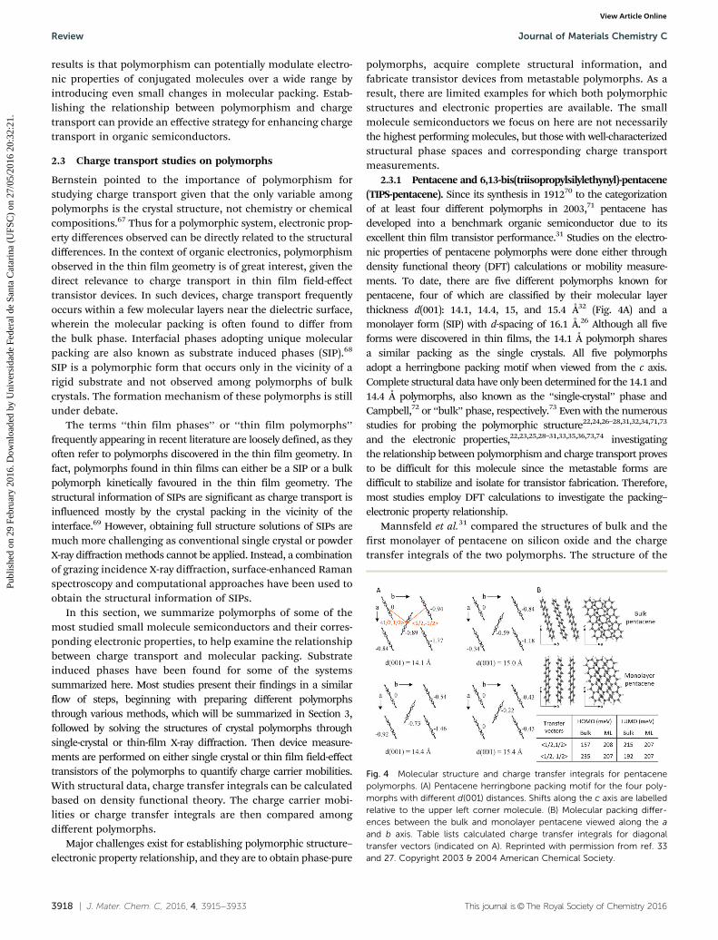
2.3.1 Pentacene and 6,13-bis(triisopropylsilylethynyl)-pentacene(TIPS-pentacene). Since its synthesis in 191270 to the categorizationof at least four different polymorphs in 2003,71 pentacene hasdeveloped into a benchmark organic semiconductor due to itsexcellent thin film transistor performance.31 Studies on the electro-nic properties of pentacene polymorphs were done either throughdensity functional theory (DFT) calculations or mobility measure-ments. To date, there are five different polymorphs known forpentacene, four of which are classified by their molecular layerthickness d(001): 14.1, 14.4, 15, and 15.4 Å32 (Fig. 4A) and amonolayer form (SIP) with d-spacing of 16.1 Å.26 Although all fiveforms were discovered in thin films, the 14.1 Å polymorph sharesa similar packing as the single crystals. All five polymorphsadopt a herringbone packing motif when viewed from the c axis.Complete structural data have only been determined for the 14.1 and14.4 Å polymorphs, also known as the ‘‘single-crystal’’ phase andCampbell,72 or ‘‘bulk’’ phase, respectively.73 Even with the numerousstudies for probing the polymorphic structure22,24,26–28,31,32,34,71,73
and the electronic properties,22,23,25,28–31,33,35,36,73,74 investigatingthe relationship between polymorphism and charge transport provesto be difficult for this molecule since the metastable forms aredifficult to stabilize and isolate for transistor fabrication. Therefore,most studies employ DFT calculations to investigate the packing–electronic property relationship.
Mannsfeld et al.31 compared the structures of bulk and thefirst monolayer of pentacene on silicon oxide and the chargetransfer integrals of the two polymorphs. The structure of the
Fig. 4 Molecular structure and charge transfer integrals for pentacenepolymorphs. (A) Pentacene herringbone packing motif for the four poly-morphs with different d(001) distances. Shifts along the c axis are labelledrelative to the upper left corner molecule. (B) Molecular packing differ-ences between the bulk and monolayer pentacene viewed along the aand b axis. Table lists calculated charge transfer integrals for diagonaltransfer vectors (indicated on A). Reprinted with permission from ref. 33and 27. Copyright 2003 & 2004 American Chemical Society.
Review Journal of Materials Chemistry C
Publ
ishe
d on
29
Febr
uary
201
6. D
ownl
oade
d by
Uni
vers
idad
e Fe
dera
l de
Sant
a C
atar
ina
(UFS
C)
on 2
7/05
/201
6 20
:32:
21.
View Article Online
This journal is©The Royal Society of Chemistry 2016 J. Mater. Chem. C, 2016, 4, 3915--3933 | 3919
first monolayer is significant since charge transport predomi-nantly occurs at the semiconductor–dielectric interface in afield-effect transistor device. Grazing incidence X-ray diffrac-tion (GIXD) in combination with thin film structure refinementwas utilized to determine the molecular packing of the mono-layer. As seen from Fig. 4B, the main difference between themonolayer and bulk pentacene is evident in that the monolayerform is upright out-of-plane, in contrast to the tilted moleculesin the bulk form.
Quantum chemical calculations were performed on penta-cene dimers to compare the transfer integrals. The edge-to-faceinteractions for the monolayer form along the diagonals, ortransfer vectors h1/2,1/2i and h1/2,�1/2i, indicating a moreequivalent transfer integral of 208 meV and 207 meV for holetransport, compared to 157 meV and 235 meV for the bulk(Fig. 4B). Generally for a combined rate process, the sloweststep limits overall rate of transport. Therefore charge transportis expected to be more efficient when transfer integrals aremore balanced along different directions. As a result, themonolayer pentacene form may have more efficient chargetransport compared to the bulk, and these observations wereconsistent with the higher charge mobility from thin film thansingle crystal transistors. These results represent a significantstep towards understanding the structural origin of high per-formance in pentacene thin-film transistors.
In 2001, Anthony et al.75 introduced the triisopropylsilylethynyl(TIPS) group to the pentacene core to increase solubility incommon organic solvents and to enhance intermolecular overlap.Indeed, TIPS-pentacene is very soluble in most organic solvents,and interestingly, the introduction of the bulky TIPS side chainchanged the packing motif of the molecule from herringbone tobrick-wall stacking. A significant decrease in interplanar spacingof the aromatic rings was observed from 6.27 Å in bare penta-cene to 3.47 Å in TIPS-pentacene. Polymorphs of this compoundhave recently been under study, with several polymorphssuccessfully stabilized.
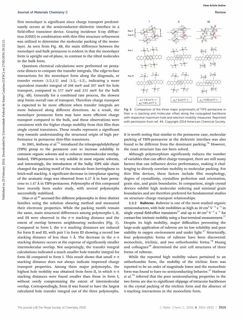
Diao et al.43 accessed five different polymorphs in three distinctfamilies using the solution shearing method and measuredtheir electronic properties. While the packing motifs remainthe same, main structural differences among polymorphs I, II,and III were observed in the p–p stacking distance and theextent of overlap between neighbouring molecules (Fig. 5).Compared to form I, the p–p stacking distances are reducedfor form II and III, with pair I in form III showing a record lowstacking distance of less than 3 Å. The decrease in the p–pstacking distance occurs at the expense of significantly smallerintermolecular overlap. Not surprisingly, the transfer integralcalculations indicated a much smaller hole transfer integral forform III compared to form I. This result shows that small p–pstacking distance does not always indicate improved chargetransport properties. Among three major polymorphs, thehighest hole mobility was obtained from form II, in which p–pstacking distances were found smaller than those in form I,without overly compromising the extent of intermolecularoverlap. Correspondingly, form II was found to have the largestcalculated hole transfer integral out of the three polymorphs.
It is worth noting that similar to the pentacene case, molecularpacking of TIPS-pentacene at the dielectric interface was alsofound to be different from the dominant packing.76 However,the exact structure has not been solved.
Although polymorphism significantly reduces the numberof variables that can affect charge transport, there are still manyfactors that can influence device performance, making it chal-lenging to directly correlate mobility to molecular packing. Forthin film devices, these factors include film morphology,degree of crystallinity, crystalline perfection and orientation,grain size, and grain boundaries. In comparison, single crystaldevices exhibit high molecular ordering and minimal grainboundaries and are therefore preferred for fundamental studieson structure–charge transport relationships.
2.3.2 Rubrene. Rubrene is one of the most studied organicsemiconductors, with hole mobilities as high as 20 cm2 V�1 s�1 insingle crystal field-effect transistors37 and up to 40 cm2 V�1 s�1 forcontact-free intrinsic mobility using a four-terminal measurement.77
Despite its high mobility, major difficulties preventing thelarge-scale application of rubrene are its low solubility and poorstability in oxygen environment and under light.37 Structurally,four polymorphic forms of rubrene have been discovered:monoclinic, triclinic, and two orthorhombic forms.78 Huangand colleagues38 determined the unit cell structures of threeforms of rubrene.
While the reported high mobility values pertained to anorthorhombic form, the mobility of the triclinic form wasreported to be an order of magnitude lower and the monoclinicform was found to have no semiconducting behavior.37 Hathwaret al.79 inferred that the poor semiconducting properties in thetwo forms are due to significant slippage of tetracene backbonesin the crystal packing of the triclinic form and the absence ofp-stacking interactions in the monoclinic form.
Fig. 5 Comparison of the three major polymorphs of TIPS-pentacene intheir p–p stacking and molecular offset along the conjugated backbonewith respective maximum hole and electron mobility measured. Reprintedwith permission from ref. 44. Copyright 2014 American Chemical Society.
Journal of Materials Chemistry C Review
Publ
ishe
d on
29
Febr
uary
201
6. D
ownl
oade
d by
Uni
vers
idad
e Fe
dera
l de
Sant
a C
atar
ina
(UFS
C)
on 2
7/05
/201
6 20
:32:
21.
View Article Online
3920 | J. Mater. Chem. C, 2016, 4, 3915--3933 This journal is©The Royal Society of Chemistry 2016
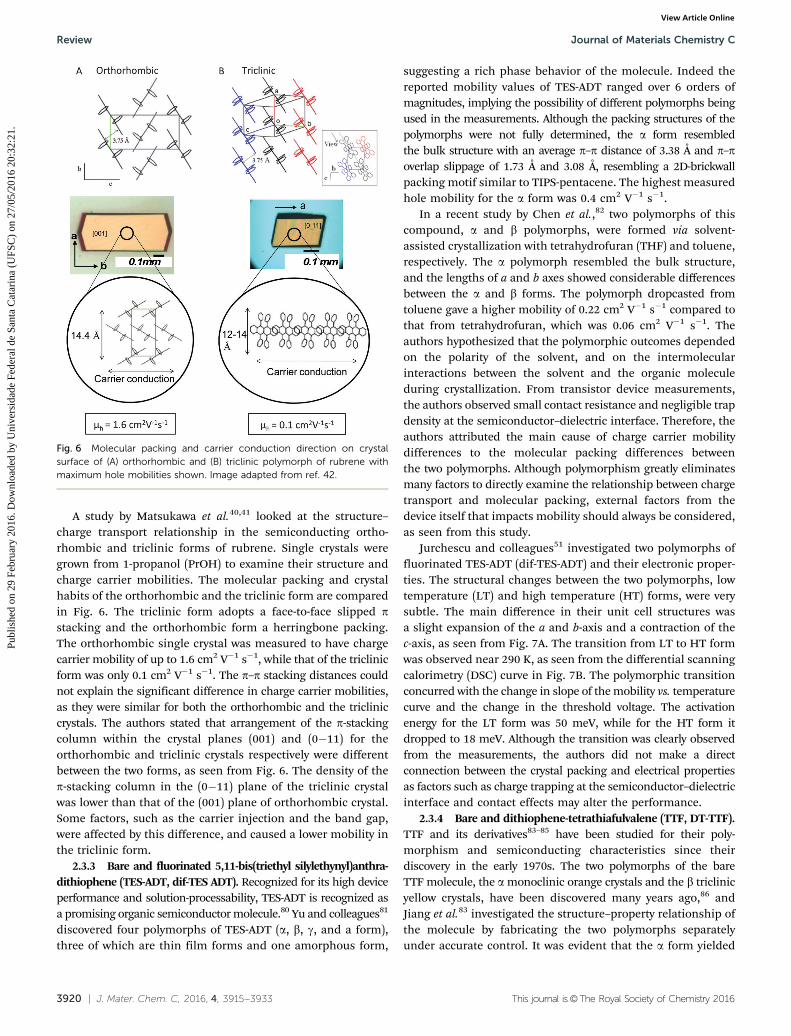
A study by Matsukawa et al.40,41 looked at the structure–charge transport relationship in the semiconducting ortho-rhombic and triclinic forms of rubrene. Single crystals weregrown from 1-propanol (PrOH) to examine their structure andcharge carrier mobilities. The molecular packing and crystalhabits of the orthorhombic and the triclinic form are comparedin Fig. 6. The triclinic form adopts a face-to-face slipped pstacking and the orthorhombic form a herringbone packing.The orthorhombic single crystal was measured to have chargecarrier mobility of up to 1.6 cm2 V�1 s�1, while that of the triclinicform was only 0.1 cm2 V�1 s�1. The p–p stacking distances couldnot explain the significant difference in charge carrier mobilities,as they were similar for both the orthorhombic and the tricliniccrystals. The authors stated that arrangement of the p-stackingcolumn within the crystal planes (001) and (0�11) for theorthorhombic and triclinic crystals respectively were differentbetween the two forms, as seen from Fig. 6. The density of thep-stacking column in the (0�11) plane of the triclinic crystalwas lower than that of the (001) plane of orthorhombic crystal.Some factors, such as the carrier injection and the band gap,were affected by this difference, and caused a lower mobility inthe triclinic form.
2.3.3 Bare and fluorinated 5,11-bis(triethyl silylethynyl)anthra-dithiophene (TES-ADT, dif-TES ADT). Recognized for its high deviceperformance and solution-processability, TES-ADT is recognized asa promising organic semiconductor molecule.80 Yu and colleagues81
discovered four polymorphs of TES-ADT (a, b, g, and a form),three of which are thin film forms and one amorphous form,
suggesting a rich phase behavior of the molecule. Indeed thereported mobility values of TES-ADT ranged over 6 orders ofmagnitudes, implying the possibility of different polymorphs beingused in the measurements. Although the packing structures of thepolymorphs were not fully determined, the a form resembledthe bulk structure with an average p–p distance of 3.38 Å and p–poverlap slippage of 1.73 Å and 3.08 Å, resembling a 2D-brickwallpacking motif similar to TIPS-pentacene. The highest measuredhole mobility for the a form was 0.4 cm2 V�1 s�1.
In a recent study by Chen et al.,82 two polymorphs of thiscompound, a and b polymorphs, were formed via solvent-assisted crystallization with tetrahydrofuran (THF) and toluene,respectively. The a polymorph resembled the bulk structure,and the lengths of a and b axes showed considerable differencesbetween the a and b forms. The polymorph dropcasted fromtoluene gave a higher mobility of 0.22 cm2 V�1 s�1 compared tothat from tetrahydrofuran, which was 0.06 cm2 V�1 s�1. Theauthors hypothesized that the polymorphic outcomes dependedon the polarity of the solvent, and on the intermolecularinteractions between the solvent and the organic moleculeduring crystallization. From transistor device measurements,the authors observed small contact resistance and negligible trapdensity at the semiconductor–dielectric interface. Therefore, theauthors attributed the main cause of charge carrier mobilitydifferences to the molecular packing differences betweenthe two polymorphs. Although polymorphism greatly eliminatesmany factors to directly examine the relationship between chargetransport and molecular packing, external factors from thedevice itself that impacts mobility should always be considered,as seen from this study.
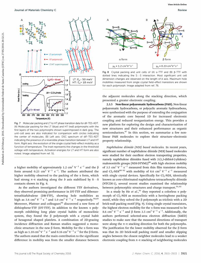
Jurchescu and colleagues51 investigated two polymorphs offluorinated TES-ADT (dif-TES-ADT) and their electronic proper-ties. The structural changes between the two polymorphs, lowtemperature (LT) and high temperature (HT) forms, were verysubtle. The main difference in their unit cell structures wasa slight expansion of the a and b-axis and a contraction of thec-axis, as seen from Fig. 7A. The transition from LT to HT formwas observed near 290 K, as seen from the differential scanningcalorimetry (DSC) curve in Fig. 7B. The polymorphic transitionconcurred with the change in slope of the mobility vs. temperaturecurve and the change in the threshold voltage. The activationenergy for the LT form was 50 meV, while for the HT form itdropped to 18 meV. Although the transition was clearly observedfrom the measurements, the authors did not make a directconnection between the crystal packing and electrical propertiesas factors such as charge trapping at the semiconductor–dielectricinterface and contact effects may alter the performance.
2.3.4 Bare and dithiophene-tetrathiafulvalene (TTF, DT-TTF).TTF and its derivatives83–85 have been studied for their poly-morphism and semiconducting characteristics since theirdiscovery in the early 1970s. The two polymorphs of the bareTTF molecule, the a monoclinic orange crystals and the b triclinicyellow crystals, have been discovered many years ago,86 andJiang et al.83 investigated the structure–property relationship ofthe molecule by fabricating the two polymorphs separatelyunder accurate control. It was evident that the a form yielded
Fig. 6 Molecular packing and carrier conduction direction on crystalsurface of (A) orthorhombic and (B) triclinic polymorph of rubrene withmaximum hole mobilities shown. Image adapted from ref. 42.
Review Journal of Materials Chemistry C
Publ
ishe
d on
29
Febr
uary
201
6. D
ownl
oade
d by
Uni
vers
idad
e Fe
dera
l de
Sant
a C
atar
ina
(UFS
C)
on 2
7/05
/201
6 20
:32:
21.
View Article Online
This journal is©The Royal Society of Chemistry 2016 J. Mater. Chem. C, 2016, 4, 3915--3933 | 3921
a higher mobility of approximately 1.2 cm2 V�1 s�1 and the bform around 0.23 cm2 V�1 s�1. The authors attributed thehigher mobility observed to the packing of the a form, whichhad strong p–p stacking along the b axis stabilized by S� � �Scontacts shown in Fig. 8.
As the authors investigated the different TTF derivatives,they observed promising performance in DT-TTF and dibenzo-tetrathiafulvalene (DB-TTF), showing hole mobilities ashigh as 3.6 cm2 V�1 s�1 and 1.0 cm2 V�1 s�1 respectively.84,85
Moreover, Pfattner and colleagues84 discovered a new form ofdithiophene-TTF (DT-TTF). In addition to the known a poly-morph exhibiting long plate crystal habits of monoclinicsystem, they found the b polymorph with a crystal habitof hexagonal shaped platelets. A combination of 2D-grazingincidence diffraction and Raman studies suggested a mono-clinic structure in the new b form. Mobility for the a form wasas high as 1.18 cm2 V�1 s�1 and 0.16 cm2 V�1 s�1 for the b form.The authors stated that the main contribution to the significantdifference in mobility was from the smaller distance between
the adjacent molecules along the stacking direction, whichpresented a greater electronic coupling.
2.3.5 Non-linear polyaromatic hydrocarbons (PAH). Non-linearpolyaromatic hydrocarbons, or polycyclic aromatic hydrocarbons,were synthesized with the purpose of extending the conjugationof the aromatic core beyond 1D for increased electroniccoupling and reduced reorganization energy. This provides anew platform for exploring the design and characterization ofnew structures and their enhanced performance as organicsemiconductors.87 In this section, we summarize a few non-linear PAH molecules to explore their structure–electronicproperty relationship.
Naphthalene diimide (NDI) based molecules. In recent years,significant number of naphthalene diimide (NDI) based moleculeswere studied for their excellent electron transporting properties,namely naphthalene diimides fused with 2-(1,3-dithiol-2-ylidene)-malononitrile groups (NDI-DTYM2)88 with high electron mobilityof 3.5 cm2 V�1 s�1 measured from thin film transistor devices,and Cl2-NDI88–92 with mobility of 8.6 cm2 V�1 s�1 measuredwith single crystal devices. Specifically for Cl2-NDI, identicallyknown as core-chlorinated naphthalene tetracarboxylic diimide(NTCDI-1), several recent studies examined the relationshipbetween polymorphic structures and charge transport.91,92
In a study by He et al.,91 they reported a colorless a poly-morph of Cl2-NDI as monoclinic with a herringbone packingmotif, while they solved the b polymorph as triclinic with a 2Dbrick-wall packing motif (Fig. 9). Using single crystal transistors,the highest electron mobility for the a form was measured to be8.6 cm2 V�1 s�1 and b form 3.5 cm2 V�1 s�1. Additionally, theauthors performed selected-area electron diffraction (SAED)studies to make sure that the measured directions of transportwere along the p–p stacking direction for both the polymorphs.The justification for the lower mobility observed for the b formwas that its 2D brick-wall packing motif and smaller slippingangles between the closest neighbor molecules lead to a weakerelectronic coupling from p–p stacking of neighboring molecules
Fig. 7 Molecular packing and LT to HT phase transition data for dif-TES-ADT.(A) Molecular packing for the LT (blue) and HT (red) polymorphs with thefirst layers of the two polymorphs shown superimposed in dark gray. Theunit-cell axes are also indicated for comparison with circles indicatingthe center of molecules. (B) Left axis: DSC spectrum of diF-TES-ADTindicating the presence of a reversible phase transition between LT and HTform. Right axis: the evolution of the single crystal field-effect mobility as afunction of temperature. The inset represents the changes in the thresholdvoltage with temperature. Activation energies for LT and HT form are alsonoted. Image adapted from ref. 51.
Fig. 8 Crystal packing and unit cells of (A) a-TTF and (B) b-TTF withdotted lines indicating the S� � �S interaction. Most significant unit celldimension changes are observed on the length of b axis. Maximum holemobilities measured from single crystal field-effect transistors are shownfor each polymorph. Image adapted from ref. 76.
Journal of Materials Chemistry C Review
Publ
ishe
d on
29
Febr
uary
201
6. D
ownl
oade
d by
Uni
vers
idad
e Fe
dera
l de
Sant
a C
atar
ina
(UFS
C)
on 2
7/05
/201
6 20
:32:
21.
View Article Online
3922 | J. Mater. Chem. C, 2016, 4, 3915--3933 This journal is©The Royal Society of Chemistry 2016
and a longer percolation pathway for electrons to cross the unitcell. In comparison, the a form contained more directionalcoupling to facilitate electron transport along the p stacks inthe crystal.
7,14-Bis((trimethylsilyl)ethynyl)-dibenzo[b,def]-chrysene (TMS-DBC).Stevens and researchers93 investigated the phase space andelectronic properties of TMS-DBC to study the effect of struc-ture on charge transport. A LT form and a HT form wereinduced using a variety of crystal fabrication processes. TheLT form was crystallized as fine red needles with 1D slippedstack motif, while the HT form took the form of large yellowplatelets with 2D brickwork motif (Fig. 10). From single crystalfield-effect transistor measurements, the LT form yieldedmaximum hole mobility of 0.028 cm2 V�1 s�1 and the HT form2.1 cm2 V�1 s�1. However, direct comparison of charge transportbetween the two polymorphs was difficult, as most of LTcrystals used for device were crystallized from solution, whichproduced crystals with increased surface roughness and lowerpurity, compared to the HT crystals fabricated from physicalvapor transport (PVT).
Additionally, the authors investigated the electronic cou-plings and band structures of the polymorphs to understandtheir intrinsic charge transport properties. They concluded thatthe much higher mobility of the HT form was due to its higherdimensionality for charge transport: the LT polymorph had asingle large hole electronic coupling (t in Fig. 10A) while the HTpolymorph had two large hole electronic couplings (t1 and t2
in Fig. 10B) to allow charge carriers to take alternative pathways
around defects or trap states. It is worth noting that polymorphswith higher dimensionality (e.g. 2D brick-wall packing vs. 1D slip-stack) do not necessarily exhibit better charge transport proper-ties, such as the case of Cl2-NDI where the electronic couplingis reduced in 2D brick-wall packing.
Contorted hexabenzocoronene (c-HBC). Hiszpanski et al.52
accessed the rich phase space of c-HBC by decoupling filmformation and structure development via post-deposition pro-cesses including thermal and solvent vapor annealing. Theresearchers determined the different structures of the polymorphsfrom GIXD and quantified the crystal orientation distributionwith Herman’s orientation function. In addition to an alreadyknown monoclinic P21/c polymorph I, they discovered a pre-viously unreported polymorph II by solvent vapor annealing.Although the detailed structure of polymorph II was not deter-mined, it was found that the new polymorph belonged to thetriclinic space group. Thermal annealing of this new polymorphalso yielded another structure, polymorph II0 which was inferredto be in the same triclinic system.
Generally the highest hole mobility determined from polymorphI was 2 � 10�3 cm2 V�1 s�1, polymorph II 3.3 � 10�4 cm2 V�1 s�1,and polymorph II0 3.6 � 10�3 cm2 V�1 s�1. The significance ofthis study is that the effect of crystal packing and orientationwere decoupled by the application of post deposition processingand was independently correlated to changes in charge transportproperties. This step is important for an accurate comparison ofthe structure with charge transport, as it eliminates the effect ofother factors such as grain size that may affect performanceif different deposition methods or substrates are used to accessthe different polymorphs.
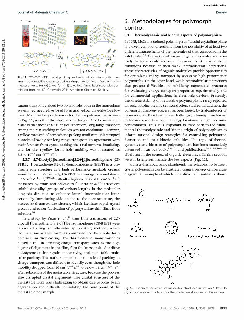
2.3.6 Thieno[3,2-b]thiophene–thiazolo[5,4-d]thiazole (TT–TzTz–TT). By combining thieno[3,2-b]thiophene (TT) andthiazolo[5,4-d]thiazole (TzTz), Schneider et al.94 synthesized anovel molecule for studying charge transport in relationshipwith molecular packing. Single crystals grown from physical
Fig. 9 Crystal packing and maximum electron mobility values measuredfrom single crystal field-effect transistors of Cl2-NDI for (A) a monoclinicform and (B) b triclinic form Image adapted from ref. 84.
Fig. 10 TMS-DBC crystal images and molecular packing structures. Thered arrows indicate transfer vectors with largest calculated electroniccouplings for the (A) LT and (B) HT polymorph. Maximum hole mobilitiesobtained from single crystal organic field-effect transistor measurementsare shown. Reprinted with permission from ref. 86. Copyright 2015American Chemical Society.
Review Journal of Materials Chemistry C
Publ
ishe
d on
29
Febr
uary
201
6. D
ownl
oade
d by
Uni
vers
idad
e Fe
dera
l de
Sant
a C
atar
ina
(UFS
C)
on 2
7/05
/201
6 20
:32:
21.
View Article Online
This journal is©The Royal Society of Chemistry 2016 J. Mater. Chem. C, 2016, 4, 3915--3933 | 3923
vapour transport yielded two polymorphs both in the monoclinicsystem: red needle-like 1-red form and yellow plate-like 1-yellowform. Main packing differences for the two polymorphs, as seenin Fig. 11, was that the slip-stack packing of 1-red consisted ofp-stacks that meet at 69.31 angles. Therefore, long-range transportamong the p–p stacking molecules was not continuous. However,1-yellow consisted of herringbone packing motif with uninterruptedp-stacks allowing for long-range transport. In agreement withthe inferences from crystal packing, the 1-red form was insulating,and for the 1-yellow form, hole mobility was measured as3.3 � 10�3 cm2 V�1 s�1.
2.3.7 2,7-Dioctyl[1]benzothieno[3,2-b][1]benzothiophene (C8-BTBT). [1]benzothieno[3,2-b][1]-benzothiophene (BTBT) is a pro-mising core structure as a high performance air-stable organicsemiconductor. Particularly, C8-BTBT has average hole mobility of3–16 cm2 V�1 s�1,50,95,96 with ultra high mobility of 43 cm2 V�1 s�1
measured by Yuan and colleagues.50 Ebata et al.97 introducedsolubilizing alkyl groups of various lengths in the molecularlong-axis direction to enhance lateral intermolecular inter-action. By introducing side chains to the core structure, themolecular distances are shorter, which facilitate rapid crystalgrowth and easier fabrication of polycrystalline thin films fromsolution.96
In a study by Yuan et al.,50 thin film transistors of 2,7-dioctyl[1]benzothieno[3,2-b][1]benzothiophene (C8-BTBT) werefabricated using an off-center spin-coating method, whichled to a metastable form as compared to the stable formobtained via drop-casting. For this molecule, many variablesplayed a role in affecting charge transport, such as the highdegree of alignment in the film, film thickness, role of additivepolystyrene on inter-grain connectivity, and metastable mole-cular packing. The authors stated that the role of packing incharge transport was difficult to identify even though the holemobility dropped from 26 cm2 V�1 s�1 to below 4.1 cm2 V�1 s�1
after relaxation of the metastable structure, because the processalso disrupted crystal alignment. The crystal structure of themetastable form was challenging to obtain due to X-ray beamdegradation and difficulty in isolating the pure phase of themetastable polymorph.
3. Methodologies for polymorphcontrol3.1 Thermodynamic and kinetic aspects of polymorphism
In 1965, McCrone defined polymorph as ‘‘a solid crystalline phaseof a given compound resulting from the possibility of at least twodifferent arrangements of the molecules of that compound in thesolid state’’.98 As mentioned earlier, organic molecules are morelikely to form easily accessible polymorphs at near ambientconditions because of their weak intermolecular interactions.These characteristics of organic molecules provide opportunitiesfor optimizing charge transport by accessing high performancepolymorphs. On the other hand, weak intermolecular interactionsalso present difficulties in stabilizing metastable structuresfor evaluating charge transport properties experimentally andfor commercial applications in electronic devices. Presently,the kinetic stability of metastable polymorphs is rarely reportedfor polymorphic organic semiconductors studied. In addition, thepolymorph discovery process has been largely by trial-and-error orby serendipity. Faced with these challenges, polymorphism has yetto become a widely adopted strategy for attaining high electronicperformances. Thus it is important to trace back to the funda-mental thermodynamic and kinetic origin of polymorphism toinform rational design strategies for controlling polymorphformation and their kinetic stabilities. The topic of thermo-dynamics and kinetics of polymorphism has been extensivelydiscussed in various books98–101 and publications,20,21,67,102–108
albeit not in the context of organic electronics. In this section,we will briefly summarize the key aspects (Fig. 12).
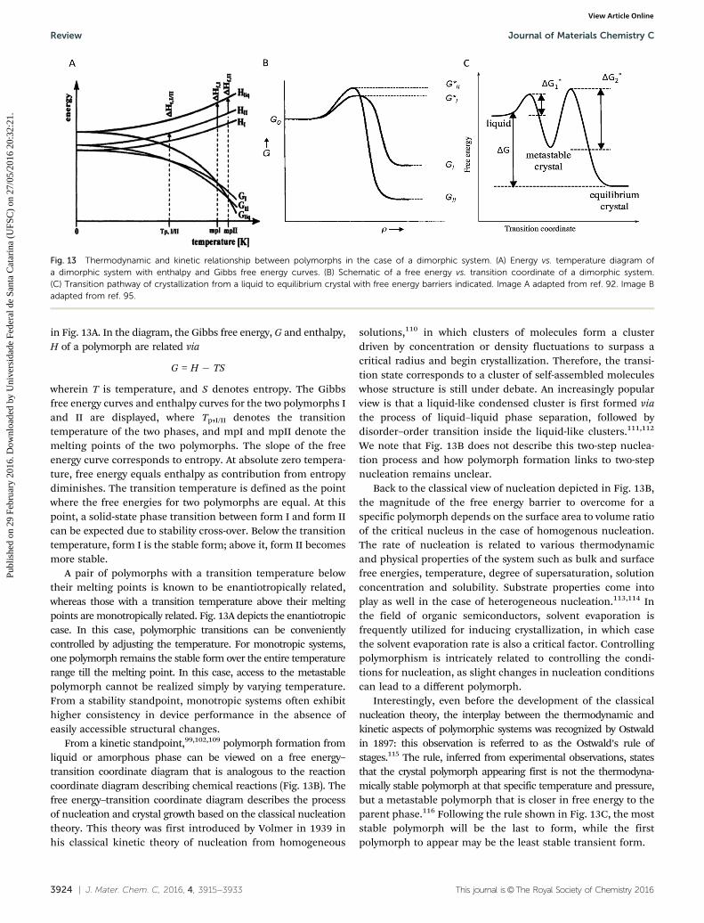
From a thermodynamic standpoint, the relationship betweencrystal polymorphs can be illustrated using an energy-temperaturediagram, an example of which for a dimorphic system is shown
Fig. 11 TT–TzTz–TT crystal packing and unit cell structure with max-imum hole mobility characterized via single crystal field-effect transistormeasurements for (A) 1-red form (B) 1-yellow form. Reprinted with per-mission from ref. 52. Copyright 2014 American Chemical Society.
Fig. 12 Chemical structures of molecules introduced in Section 3. Refer toFig. 2 for chemical structures of other molecules discussed in this section.
Journal of Materials Chemistry C Review
Publ
ishe
d on
29
Febr
uary
201
6. D
ownl
oade
d by
Uni
vers
idad
e Fe
dera
l de
Sant
a C
atar
ina
(UFS
C)
on 2
7/05
/201
6 20
:32:
21.
View Article Online
3924 | J. Mater. Chem. C, 2016, 4, 3915--3933 This journal is©The Royal Society of Chemistry 2016
in Fig. 13A. In the diagram, the Gibbs free energy, G and enthalpy,H of a polymorph are related via
G = H � TS
wherein T is temperature, and S denotes entropy. The Gibbsfree energy curves and enthalpy curves for the two polymorphs Iand II are displayed, where Tp,I/II denotes the transitiontemperature of the two phases, and mpI and mpII denote themelting points of the two polymorphs. The slope of the freeenergy curve corresponds to entropy. At absolute zero tempera-ture, free energy equals enthalpy as contribution from entropydiminishes. The transition temperature is defined as the pointwhere the free energies for two polymorphs are equal. At thispoint, a solid-state phase transition between form I and form IIcan be expected due to stability cross-over. Below the transitiontemperature, form I is the stable form; above it, form II becomesmore stable.
A pair of polymorphs with a transition temperature belowtheir melting points is known to be enantiotropically related,whereas those with a transition temperature above their meltingpoints are monotropically related. Fig. 13A depicts the enantiotropiccase. In this case, polymorphic transitions can be convenientlycontrolled by adjusting the temperature. For monotropic systems,one polymorph remains the stable form over the entire temperaturerange till the melting point. In this case, access to the metastablepolymorph cannot be realized simply by varying temperature.From a stability standpoint, monotropic systems often exhibithigher consistency in device performance in the absence ofeasily accessible structural changes.
From a kinetic standpoint,99,102,109 polymorph formation fromliquid or amorphous phase can be viewed on a free energy–transition coordinate diagram that is analogous to the reactioncoordinate diagram describing chemical reactions (Fig. 13B). Thefree energy–transition coordinate diagram describes the processof nucleation and crystal growth based on the classical nucleationtheory. This theory was first introduced by Volmer in 1939 inhis classical kinetic theory of nucleation from homogeneous
solutions,110 in which clusters of molecules form a clusterdriven by concentration or density fluctuations to surpass acritical radius and begin crystallization. Therefore, the transi-tion state corresponds to a cluster of self-assembled moleculeswhose structure is still under debate. An increasingly popularview is that a liquid-like condensed cluster is first formed viathe process of liquid–liquid phase separation, followed bydisorder–order transition inside the liquid-like clusters.111,112
We note that Fig. 13B does not describe this two-step nuclea-tion process and how polymorph formation links to two-stepnucleation remains unclear.
Back to the classical view of nucleation depicted in Fig. 13B,the magnitude of the free energy barrier to overcome for aspecific polymorph depends on the surface area to volume ratioof the critical nucleus in the case of homogenous nucleation.The rate of nucleation is related to various thermodynamicand physical properties of the system such as bulk and surfacefree energies, temperature, degree of supersaturation, solutionconcentration and solubility. Substrate properties come intoplay as well in the case of heterogeneous nucleation.113,114 Inthe field of organic semiconductors, solvent evaporation isfrequently utilized for inducing crystallization, in which casethe solvent evaporation rate is also a critical factor. Controllingpolymorphism is intricately related to controlling the condi-tions for nucleation, as slight changes in nucleation conditionscan lead to a different polymorph.
Interestingly, even before the development of the classicalnucleation theory, the interplay between the thermodynamic andkinetic aspects of polymorphic systems was recognized by Ostwaldin 1897: this observation is referred to as the Ostwald’s rule ofstages.115 The rule, inferred from experimental observations, statesthat the crystal polymorph appearing first is not the thermodyna-mically stable polymorph at that specific temperature and pressure,but a metastable polymorph that is closer in free energy to theparent phase.116 Following the rule shown in Fig. 13C, the moststable polymorph will be the last to form, while the firstpolymorph to appear may be the least stable transient form.
Fig. 13 Thermodynamic and kinetic relationship between polymorphs in the case of a dimorphic system. (A) Energy vs. temperature diagram ofa dimorphic system with enthalpy and Gibbs free energy curves. (B) Schematic of a free energy vs. transition coordinate of a dimorphic system.(C) Transition pathway of crystallization from a liquid to equilibrium crystal with free energy barriers indicated. Image A adapted from ref. 92. Image Badapted from ref. 95.
Review Journal of Materials Chemistry C
Publ
ishe
d on
29
Febr
uary
201
6. D
ownl
oade
d by
Uni
vers
idad
e Fe
dera
l de
Sant
a C
atar
ina
(UFS
C)
on 2
7/05
/201
6 20
:32:
21.
View Article Online
This journal is©The Royal Society of Chemistry 2016 J. Mater. Chem. C, 2016, 4, 3915--3933 | 3925
3.2 Methods of polymorph access and control
The challenge of controlling polymorph formation is multi-fold, given the lack of thermodynamic and kinetic informationsummarized in the previous section, the high sensitivityof nucleation to numerous experimental conditions, and thetransient nature of metastable phases, etc. Some methodsdiscussed in this section are analogous to the methods exten-sively employed in the pharmaceuticals field, which shares thecommon goal in controlling and accessing different polymorphs.Polymorphism of drugs has been the subject of great researchfocus, as drug efficacy and bioavailability are affected.117 Someof the polymorph control methods applied to organic semi-conductors include templating, solvent selection, crystallizationkinetics control, thin film confinement, post deposition control,and other methods such as pressure induced, mechanicallytriggered, flow-assisted, vapour-sublimed in air, or light inducedpolymorph formation and transition. Each of these methods willbe discussed in the following sections.
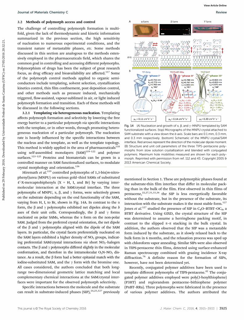
3.2.1 Templating via heterogeneous nucleation. Templatingaffects polymorph formation and selectivity by lowering the freeenergy barrier to a particular polymorph via specific interactionswith the template, or in other words, through promoting hetero-geneous nucleation of a particular polymorph. The nucleationrate is heavily influenced by the specific interactions betweenthe nucleus and the template, as well as the template topology.This method is widely applied in the area of pharmaceuticals118
using self-assembled monolayers (SAM)119–122 and polymersurfaces.123–125 Proteins and biomaterials can be grown in acontrolled manner on SAM functionalized surfaces, to modulatecrystal morphology and orientation.126
Hiremath et al.119 controlled polymorphs of 1,3-bis(m-nitro-phenyl)urea (MNPU) on various gold–thiol SAMs of substituted40-X-mercaptobiphenyls (X = H, I, and Br) by varying inter-molecular interaction at the SAM/crystal interface. The threepolymorphs of MNPU, a, b, and g forms, were selectively grownon the substrate depending on the end functionality of the SAM,varying from H, I, to Br, shown in Fig. 14A. In contrast to the aform, the b and g polymorphs exhibited net dipoles along the baxes of their unit cells. Correspondingly, the b and g formsnucleated on polar SAMs, whereas the a form on the non-polarSAM. Judged from the preferred crystal orientation, the net dipoleof the b and g polymorphs aligned with the dipole of the SAMlayers. In particular, the crystal facets preferentially nucleated onthe SAM layers exhibited a higher density of NO2 groups, indicat-ing preferential SAM/crystal interactions via short NO2–halogencontacts. The b and g polymorphs differed slightly in the molecularconformation, and therefore in the intramolecular O2N–NO2 dis-tance. As a result, the b form had a better epitaxial match with theiodine-substituted SAM, and the g form with the bromine one.All cases considered, the authors concluded that both long-range two-dimensional geometric lattice matching and localcomplementary chemical interactions at the SAM/crystal inter-faces were important for the observed polymorph selectivity.
Specific interactions between the molecule and the substratecan result in substrate-induced phases (SIP),24,25,127 previously
mentioned in Section 1. These are polymorphic phases found atthe substrate-thin film interface that differ in molecular pack-ing than in the bulk of the film. First observed in thin films ofpentacene,22,27,31,33,36 the SIP is less energetically favorablewithout the substrate, but in the presence of the substrate, itsinteraction with the substrate makes it the most stable form.127
Jones et al.127 studied the presence of SIP in C8O–BTBT–OC8, aBTBT derivative. Using GIXD, the crystal structure of the SIPwas determined to assume a herringbone packing motif, incontrast to the slipped p–p stacking in the bulk crystal. Inaddition, the authors observed that the SIP was a metastableform induced by the substrate, as it slowly relaxed back to thebulk form in 6 months, and the relaxation process was sped upwith chloroform vapor annealing. Similar SIPs were also observedin TIPS-pentacene thin films, detected using surface-enhancedRaman spectroscopy combined with grazing incidence X-raydiffraction.76 A definite reason for the formation of SIPs,however, have not been determined yet.
Recently, conjugated polymer additives have been used totemplate different polymorphs of TIPS-pentacene.42 The conju-gated polymer additives employed were poly(3-hexylthiophene)(P3HT) and regiorandom pentacene–bithiophene polymer(PnBT–RRa). Three polymorphs were fabricated in the presenceof various polymer additives. The authors attributed the
Fig. 14 (A) Nucleation and growth of a, b, and g-MNPU templated by SAMfunctionalized surfaces. (top) Micrographs of the MNPU crystal attached toSAM substrate with a view down the b axis. Scale bars are 0.1 mm, 0.3 mm,and 0.3 mm respectively. (bottom) Schematic of the MNPU crystal/SAMinterface. Red arrows represent the direction of the molecular dipole moment.(B) Structure and unit cell parameters of the three TIPS-pentacene poly-morphs from slow solution crystallization and blended with conjugatedpolymers. Maximum hole mobilities measured are shown for each poly-morph. Reprinted with permission from ref. 112 and 43. Copyright 2005 &2013 American Chemical Society.
Journal of Materials Chemistry C Review
Publ
ishe
d on
29
Febr
uary
201
6. D
ownl
oade
d by
Uni
vers
idad
e Fe
dera
l de
Sant
a C
atar
ina
(UFS
C)
on 2
7/05
/201
6 20
:32:
21.
View Article Online
3926 | J. Mater. Chem. C, 2016, 4, 3915--3933 This journal is©The Royal Society of Chemistry 2016
polymorphic outcome to intermolecular interactions and struc-tural similarity between the organic molecule and the polymeradditive (Fig. 14B). The authors stated that a lack of structuralsimilarity between TIPS-pentacene and P3HT yielded a polymorphwith larger packing change compared to the form obtainedwithout the polymer additive. For TIPS-pentacene/PnBT–RRablend, their structural similarity and stronger intermolecularinteractions resulted in a polymorph with small structuralchanges. The intermolecular interactions were inferred fromUV-vis absorption studies. They hypothesized that the inter-molecular interactions between the polymer additive and nucleicould strongly affect the polymorphic outcome: the intermole-cular interaction guides the initial nuclei clusters to a metastablestructure that is energetically more favorable in the presence ofpolymer additives. Thus using polymer additives to tune theintermolecular interactions between the organic semiconductorand polymer template offers new opportunities for accessingvarious polymorphs.
3.2.2 Solvent-induced polymorph selectivity. The mechanismbehind solvent-induced polymorph selectivity is likely linked tothe dependence of nucleation barrier on the solvent–polymorphinterfacial free energies. At the molecular level, solvent mayinfluence the structure of the nucleus via specific interactions,thereby biasing the formation of a particular polymorph.128 Inthe pharmaceutical industry, changing crystallization solvent iscommonly practiced for high-throughput polymorph screening.
In a recent study, new polymorphs of TES-ADT were inducedby weakly polar solvents such as toluene and chloroform82
(refer to Section 2.3.3 for structure and charge transport infor-mation). The study identified high performing TES-ADT devicesreported in other sources80,129–132 to the new polymorphs. Theauthors speculated that the S–S interactions might play asignificant role in the solvent-dependent polymorphism ofTES-ADT. In addition, solvent-induced polymorph selectivitywas also observed for TIPS-pentacene.44 In this study, a differentmechanism was proposed based on the size of the solventmolecules: the larger the solvent molecules, the more likely itis to observe metastable polymorphs of TIPS-pentacene due toslower relaxation to the stable polymorph.
3.2.3 Crystallization kinetics control. It has been wellrecognized in the crystallography community that the poly-morphic outcome is sensitive to the nucleation and growthkinetics.102,124,133 The dependence of polymorphic outcome oncrystallization kinetics sometimes follows the Ostwald’s rule ofstages,124 but not always.133 In the field of organic electronics,highly kinetic crystallization conditions have been utilized foraccessing metastable polymorphs, often in thin film form. Thisapproach is sometimes referred to as kinetic trapping. Thecentral idea of this approach is to kinetically trap metastablestates via rapid crystallization or solvent evaporation.45 Wedland colleagues68 studied a kinetically trapped metastable poly-morph of DH3T that was favored at high crystallization rates,regardless of the deposition methods used.
Until recently, kinetic trapping has not been recognized asa key factor for organic semiconductor polymorph control.Taking pentacene for example, a widely accepted model
proposes the formation of the ‘‘thin-film phase’’, or SIP, up toa critical thickness of 50 nm and that the film thickness itself isthe key parameter dictating polymorph formation.27 In a studyby Wedl et al.,68 the notion that film thickness is the onlyparameter for the polymorph formation was challenged. Thinfilms of dihexylterthiophene (DH3T) were fabricated by spin-coating, dip-coating, drop-casting, and physical vapor deposition,with the crystallization speed as the key variable. Solution-baseddeposition methods controlled the speed of solvent evaporation;vacuum deposition enabled a controlled environment withcontrol of film thickness and deposition rate. Three polymorphicstructures of DH3T were discovered from the experiment andnoted as the a-phase, b-phase, and the thin film phase. Theresults indicated that the thin film phase appeared independentof the specific deposition techniques but dependent on thecrystallization speed. Specifically, the thin film phase appearedduring spin coating, drop casting with fast solvent evaporation(2 min), dip coating with high withdrawal velocity (500 mm s�1),and physical vapor deposition. Specifically for drop-casting anddip-coating, evaporation time of the solvent was a central para-meter, in that high evaporation yielded the thin film phasewhereas slow evaporation yielded either the a or the b phase.
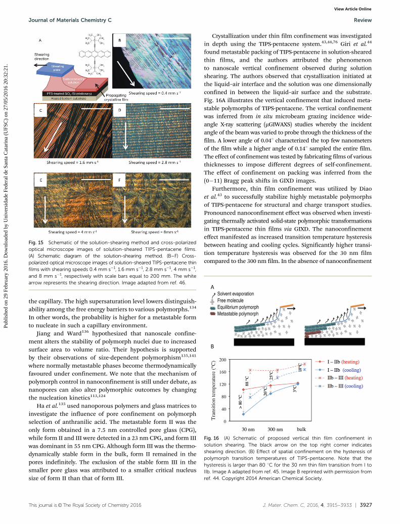
Crystallization kinetics control was also applied in a study byGiri et al.,45 wherein the solution shearing method was utilizedto fabricate thin films of TIPS-pentacene. As seen in Fig. 15,various films were fabricated as a function of shearing speed.A decrease in film thickness was observed for increase inshearing speed, and a steeper temperature gradient formed inthe thinner films. Thus solvent evaporation rate was increasedfor thinner films, resulting in faster solution flow towards thegrowing crystal front and less time for the growing crystals toreach their equilibrium state. The authors hypothesized thatfast crystallization and solvent evaporation kinetically trappedthe metastable states. These states were shown to relax to morestable states with toluene vapor annealing.
Crystallization kinetics control is a powerful method foraccessing metastable polymorphs, especially in the thin filmgeometry when kinetic trapping and thin film confinement(see following section) work in synergy. Fabricating thin filmsof metastable polymorphs could facilitate structure analysis viaX-ray diffraction and device characterization. New structural andcharge transport information are valuable for acquiring betterfundamental understanding of the structure–property relationship.
3.2.4 Nanoscale and thin film confinement. Using spatialor surface confinement to access a metastable polymorph hasbeen developed for crystallization of molecular compounds, inparticular pharmaceuticals. The confined environment hasbeen constructed using capillaries,134 nanoporous media orsurfaces such as controlled pore glass and nanostructuredpolymer surfaces,113,135–137 and microporous materials such aszeolites and polymer gels.138–140 In a study by Hilden et al., theauthors accessed six forms of 5-methyl-2-[(2-nitrophenyl)amino]-3-thiophenecarbonitrile (ROY) using capillary crystallization.The authors hypothesized that nucleation was suppressed bythe small volume available in the glass capillary tubes. As aresult, nucleation occurred at very high supersaturation level in
Review Journal of Materials Chemistry C
Publ
ishe
d on
29
Febr
uary
201
6. D
ownl
oade
d by
Uni
vers
idad
e Fe
dera
l de
Sant
a C
atar
ina
(UFS
C)
on 2
7/05
/201
6 20
:32:
21.
View Article Online
This journal is©The Royal Society of Chemistry 2016 J. Mater. Chem. C, 2016, 4, 3915--3933 | 3927
the capillary. The high supersaturation level lowers distinguish-ability among the free energy barriers to various polymorphs.134
In other words, the probability is higher for a metastable formto nucleate in such a capillary environment.
Jiang and Ward136 hypothesized that nanoscale confine-ment alters the stability of polymorph nuclei due to increasedsurface area to volume ratio. Their hypothesis is supportedby their observations of size-dependent polymorphism135,141
where normally metastable phases become thermodynamicallyfavoured under confinement. We note that the mechanism ofpolymorph control in nanoconfinement is still under debate, asnanopores can also alter polymorphic outcomes by changingthe nucleation kinetics113,124
Ha et al.135 used nanoporous polymers and glass matrices toinvestigate the influence of pore confinement on polymorphselection of anthranilic acid. The metastable form II was theonly form obtained in a 7.5 nm controlled pore glass (CPG),while form II and III were detected in a 23 nm CPG, and form IIIwas dominant in 55 nm CPG. Although form III was the thermo-dynamically stable form in the bulk, form II remained in thepores indefinitely. The exclusion of the stable form III in thesmaller pore glass was attributed to a smaller critical nucleussize of form II than that of form III.
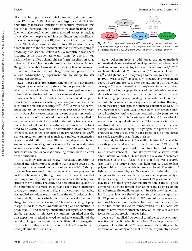
Crystallization under thin film confinement was investigatedin depth using the TIPS-pentacene system.43,44,76 Giri et al.44
found metastable packing of TIPS-pentacene in solution-shearedthin films, and the authors attributed the phenomenonto nanoscale vertical confinement observed during solutionshearing. The authors observed that crystallization initiated atthe liquid–air interface and the solution was one dimensionallyconfined in between the liquid–air surface and the substrate.Fig. 16A illustrates the vertical confinement that induced meta-stable polymorphs of TIPS-pentacene. The vertical confinementwas inferred from in situ microbeam grazing incidence wide-angle X-ray scattering (mGIWAXS) studies whereby the incidentangle of the beam was varied to probe through the thickness of thefilm. A lower angle of 0.041 characterized the top few nanometersof the film while a higher angle of 0.141 sampled the entire film.The effect of confinement was tested by fabricating films of variousthicknesses to impose different degrees of self-confinement.The effect of confinement on packing was inferred from the(0�11) Bragg peak shifts in GIXD images.
Furthermore, thin film confinement was utilized by Diaoet al.43 to successfully stabilize highly metastable polymorphsof TIPS-pentacene for structural and charge transport studies.Pronounced nanoconfinement effect was observed when investi-gating thermally activated solid-state polymorphic transformationsin TIPS-pentacene thin films via GIXD. The nanoconfinementeffect manifested as increased transition temperature hysteresisbetween heating and cooling cycles. Significantly higher transi-tion temperature hysteresis was observed for the 30 nm filmcompared to the 300 nm film. In the absence of nanoconfinement
Fig. 15 Schematic of the solution-shearing method and cross-polarizedoptical microscope images of solution-sheared TIPS-pentacene films.(A) Schematic diagram of the solution-shearing method. (B–F) Cross-polarized optical microscope images of solution-sheared TIPS-pentacene thinfilms with shearing speeds 0.4 mm s�1, 1.6 mm s�1, 2.8 mm s�1, 4 mm s�1,and 8 mm s�1, respectively with scale bars equal to 200 mm. The whitearrow represents the shearing direction. Image adapted from ref. 46.
Fig. 16 (A) Schematic of proposed vertical thin film confinement insolution shearing. The black arrow on the top right corner indicatesshearing direction. (B) Effect of spatial confinement on the hysteresis ofpolymorph transition temperatures of TIPS-pentacene. Note that thehysteresis is larger than 80 1C for the 30 nm thin film transition from I toIIb. Image A adapted from ref. 45. Image B reprinted with permission fromref. 44. Copyright 2014 American Chemical Society.
Journal of Materials Chemistry C Review
Publ
ishe
d on
29
Febr
uary
201
6. D
ownl
oade
d by
Uni
vers
idad
e Fe
dera
l de
Sant
a C
atar
ina
(UFS
C)
on 2
7/05
/201
6 20
:32:
21.
View Article Online
3928 | J. Mater. Chem. C, 2016, 4, 3915--3933 This journal is©The Royal Society of Chemistry 2016
effect, the bulk powders exhibited minimal hysteresis foundfrom DSC (Fig. 16B). The authors hypothesized that thedramatically increased transition temperature hysteresis wasdue to the increased kinetic barrier to nucleation under con-finement. The confinement effect allowed access to variousmetastable polymorphs at ambient conditions, and specifically,to a new polymorph (form III) that had not been discoveredbefore. The highly transient nature of form III was overcome bya combination of the confinement effect and kinetic trapping,68
previously discussed in Section 3.2.3. A complete phase spacemapping of the TIPS-pentacene thin films (20–100 nm) wasperformed on all five polymorphs via in situ synchrotron X-raydiffraction, in combination with molecular mechanic simulations.Using the metastable forms stabilized via thin film confinement,the authors also determined charge transport properties ofvarious polymorphs by experiment and by charge transferintegral calculations.
3.2.5 Post deposition control. One of the main advantagesof organic semiconductors is their solution processability, inwhich a variety of methods have been developed to controlpolymorphism during solution processing as discussed in theprevious sections. On the other hand, some are done post-deposition to increase crystallinity, coarsen grains, and in somecases alter the molecular packing.93,127,142–145 Solvent and thermalannealing are the most commonly used post-deposition treat-ments. For solvent vapor annealing, a certain criterion needs tobe met in terms of the molecular interactions when applied toan organic semiconductor thin film: the interactions betweenmolecule–molecule, molecule–substrate, and molecule–solventneed to be evenly balanced. The domination of one form ofinteraction makes the post deposition processing difficult.142
For example, too strong of a molecule–molecule interactioncauses the thin film to crystallize during deposition beforesolvent vapor annealing, and a strong solvent–molecule inter-action can cause the thin film to dewet from the substrate. Insuch cases thermal or solvent annealing cannot have an effecton the structures.
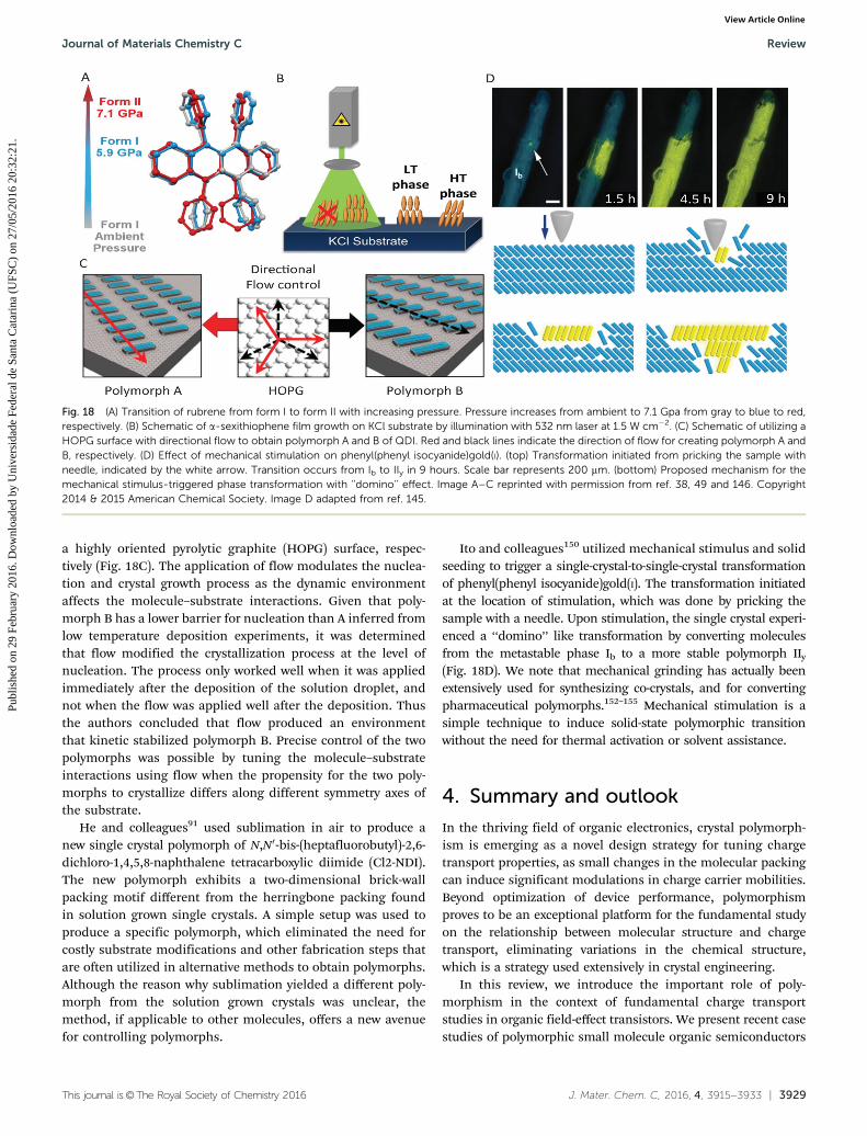
In a study by Hiszpanski et al.,52 repeated application ofthermal and solvent vapor annealing were used to access threepolymorphs of contorted hexabenzocoronene (c-HBC). Althoughthe complete structural information of the three polymorphscould not be obtained, the significance of the results was thattwo simple post deposition processes can access the rich phasespace of the molecule. The study also decoupled and quantifiedthe contributions of crystal structure and out-of-plane orientationto charge transport. Shown in Fig. 17, solvent vapor annealingwas applied to induce transition from the P21/c polymorph topolymorph II, through which effect of the crystal structure tocharge transport can be examined. Thermal annealing of poly-morph II led to a more favorable out-of-plane orientation inpolymorph II0, and thereby contributions of crystal orientationcan be evaluated in this case. The authors remarked that thepost-deposition method allowed remarkable tenability of thecrystal packing and orientation and facilitated the investigationon the affect of these two factors on the field-effect mobility inpolycrystalline thin films of c-HBC.
3.2.6 Other methods. In addition to the major methodssummarized above, a variety of novel approaches have been devel-oped to control polymorphs, including pressure-induced,37,146–149
mechanically-induced,150 flow-assisted,151 vapor-sublimed inair,91 and light-induced48 polymorph formation, to name a few.In 1994, Iwasa et al.146 applied high pressure and temperatureabove 15 GPa and 300 1C to alter the packing of C60. Wang andcolleagues149 experimented with m-xylene-solvated C60 whichpreserved the long range periodicity of the molecule even whenthe carbon cage collapsed and the carbon–carbon bonds werebroken at high pressures, revealing the importance of molecule–solvent interactions in macroscopic structural control. Recently,a high-pressure polymorph of rubrene was obtained above 6 GPaby Bergantin et al.37 (Fig. 18A). In this study, a reversible single-crystal-to-single-crystal transition occurred as the pressure wasincreased. From Hirshfeld surfaces analysis and intermolecularinteraction energy calculations, the C–H� � �p interactions werestabilized at the expense of p–p interactions, which becameenergetically less stabilizing. It highlights the power of high-pressure techniques in probing the phase space of moleculesnot easily accessible at ambient pressure.
In a study by Pithan et al.48 laser illumination influenced thegrowth process and resulted in the formation of LT and HTforms in a-sexithiophene (6T) thin films. In a dark environ-ment, a coexistence of LT and HT forms was observed, whileafter illumination with a 532 nm laser at 1.5 W cm�2, increasedpercentage of the LT form in the thin film was observed(Fig. 18B). This study shows that light can be used to biaspolymorphic outcome, which is rarely explored. The effect oflight was not caused by a different overlap of the absorptionenergies with the laser, as the two phases lied approximately atthe same energy. The reason for a favored LT phase under lightmay be due to the slightly slanted orientation of the HT phasecompared to a more upright orientation of the LT phase on theKCl substrate. The oscillator strength in HT is 20% higher thanin LT phase, in which the HT phase absorbed more light thanthe LT phase, indicating that the HT molecules experienced anincreased laser-induced heating. By examining the desorptionof the two forms at elevated temperatures, the HT form wasfound to have lower thermal stability, which was also a majorfactor for its suppression under light.
Lee et al.151 applied flow control to influence 2D polymorphselection at the liquid–solid interface. Polymorphs A and Bof quaterrylene diimide (QDI) were formed, depending on thedirection of flow along or normal to the main symmetry axes on
Fig. 17 Flow diagram of thermal and THF annealing process used to accesspolymorph P21/c, polymorph II, and polymorph II0 of c-HBC. Reprinted withpermission from ref. 52. Copyright 2014 American Chemical Society.
Review Journal of Materials Chemistry C
Publ
ishe
d on
29
Febr
uary
201
6. D
ownl
oade
d by
Uni
vers
idad
e Fe
dera
l de
Sant
a C
atar
ina
(UFS
C)
on 2
7/05
/201
6 20
:32:
21.
View Article Online
This journal is©The Royal Society of Chemistry 2016 J. Mater. Chem. C, 2016, 4, 3915--3933 | 3929
a highly oriented pyrolytic graphite (HOPG) surface, respec-tively (Fig. 18C). The application of flow modulates the nuclea-tion and crystal growth process as the dynamic environmentaffects the molecule–substrate interactions. Given that poly-morph B has a lower barrier for nucleation than A inferred fromlow temperature deposition experiments, it was determinedthat flow modified the crystallization process at the level ofnucleation. The process only worked well when it was appliedimmediately after the deposition of the solution droplet, andnot when the flow was applied well after the deposition. Thusthe authors concluded that flow produced an environmentthat kinetic stabilized polymorph B. Precise control of the twopolymorphs was possible by tuning the molecule–substrateinteractions using flow when the propensity for the two poly-morphs to crystallize differs along different symmetry axes ofthe substrate.
He and colleagues91 used sublimation in air to produce anew single crystal polymorph of N,N0-bis-(heptafluorobutyl)-2,6-dichloro-1,4,5,8-naphthalene tetracarboxylic diimide (Cl2-NDI).The new polymorph exhibits a two-dimensional brick-wallpacking motif different from the herringbone packing foundin solution grown single crystals. A simple setup was used toproduce a specific polymorph, which eliminated the need forcostly substrate modifications and other fabrication steps thatare often utilized in alternative methods to obtain polymorphs.Although the reason why sublimation yielded a different poly-morph from the solution grown crystals was unclear, themethod, if applicable to other molecules, offers a new avenuefor controlling polymorphs.
Ito and colleagues150 utilized mechanical stimulus and solidseeding to trigger a single-crystal-to-single-crystal transformationof phenyl(phenyl isocyanide)gold(I). The transformation initiatedat the location of stimulation, which was done by pricking thesample with a needle. Upon stimulation, the single crystal experi-enced a ‘‘domino’’ like transformation by converting moleculesfrom the metastable phase Ib to a more stable polymorph IIy
(Fig. 18D). We note that mechanical grinding has actually beenextensively used for synthesizing co-crystals, and for convertingpharmaceutical polymorphs.152–155 Mechanical stimulation is asimple technique to induce solid-state polymorphic transitionwithout the need for thermal activation or solvent assistance.
4. Summary and outlook
In the thriving field of organic electronics, crystal polymorph-ism is emerging as a novel design strategy for tuning chargetransport properties, as small changes in the molecular packingcan induce significant modulations in charge carrier mobilities.Beyond optimization of device performance, polymorphismproves to be an exceptional platform for the fundamental studyon the relationship between molecular structure and chargetransport, eliminating variations in the chemical structure,which is a strategy used extensively in crystal engineering.
In this review, we introduce the important role of poly-morphism in the context of fundamental charge transportstudies in organic field-effect transistors. We present recent casestudies of polymorphic small molecule organic semiconductors
Fig. 18 (A) Transition of rubrene from form I to form II with increasing pressure. Pressure increases from ambient to 7.1 Gpa from gray to blue to red,respectively. (B) Schematic of a-sexithiophene film growth on KCl substrate by illumination with 532 nm laser at 1.5 W cm�2. (C) Schematic of utilizing aHOPG surface with directional flow to obtain polymorph A and B of QDI. Red and black lines indicate the direction of flow for creating polymorph A andB, respectively. (D) Effect of mechanical stimulation on phenyl(phenyl isocyanide)gold(I). (top) Transformation initiated from pricking the sample withneedle, indicated by the white arrow. Transition occurs from Ib to IIy in 9 hours. Scale bar represents 200 mm. (bottom) Proposed mechanism for themechanical stimulus-triggered phase transformation with ‘‘domino’’ effect. Image A–C reprinted with permission from ref. 38, 49 and 146. Copyright2014 & 2015 American Chemical Society. Image D adapted from ref. 145.
Journal of Materials Chemistry C Review
Publ
ishe
d on
29
Febr
uary
201
6. D
ownl
oade
d by
Uni
vers
idad
e Fe
dera
l de
Sant
a C
atar
ina
(UFS
C)
on 2
7/05
/201
6 20
:32:
21.
View Article Online
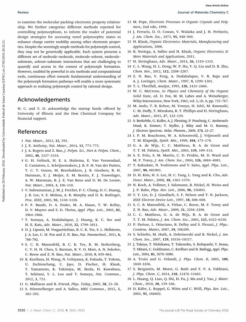
3930 | J. Mater. Chem. C, 2016, 4, 3915--3933 This journal is©The Royal Society of Chemistry 2016
to examine the molecular packing–electronic property relation-ship. We further categorize different methods reported forcontrolling polymorphism, to inform the reader of potentialdesign strategies for accessing novel polymorphic states toenhance charge carrier mobility among other electronic proper-ties. Despite the seemingly ample methods for polymorph control,they may not be generically applicable. Each system presents adifferent set of molecule–molecule, molecule–solvent, molecule–substrate, solvent–substrate interactions that are challenging toquantify and access in the context of polymorph formation.However, enabled by powerful in situ methods and computationaltools, continuous effort towards fundamental understanding ofthe polymorph formation pathways will enable a more systematicapproach to realizing polymorph control by rational design.
Acknowledgements
H. C. and Y. D. acknowledge the startup funds offered byUniversity of Illinois and the Dow Chemical Company forfinancial support.
References
1 Nat. Mater., 2013, 12, 591.2 J. E. Anthony, Nat. Mater., 2014, 13, 773–775.3 J. A. Rogers and Z. Bao, J. Polym. Sci., Part A: Polym. Chem.,
2002, 40, 3327–3334.4 G. H. Gelinck, H. E. A. Huitema, E. Van Veenendaal,
E. Cantatore, L. Schrijnemakers, J. B. P. H. Van der Putten,T. C. T. Geuns, M. Beenhakkers, J. B. Giesbers, B. H.Huisman, E. J. Meijer, E. M. Benito, F. J. Touwslager,A. W. Marsman, B. J. E. Van Rens and D. M. De Leeuw,Nat. Mater., 2004, 3, 106–110.
5 V. Subramanian, J. M. J. Frechet, P. C. Chang, D. C. Huang,J. B. Lee, S. E. Molesa, A. R. Murphy and D. R. Redinger,Proc. IEEE, 2005, 93, 1330–1338.
6 P. F. Baude, D. A. Ender, M. A. Haase, T. W. Kelley,D. V. Muyres and S. D. Theiss, Appl. Phys. Lett., 2003, 82,3964–3966.
7 T. Someya, A. Dodabalapur, J. Huang, K. C. See andH. E. Katz, Adv. Mater., 2010, 22, 3799–3811.
8 D. J. Lipomi, M. Vosgueritchian, B. C. K. Tee, S. L. Hellstrom,J. A. Lee, C. H. Fox and Z. N. Bao, Nat. Nanotechnol., 2011, 6,788–792.
9 S. C. B. Mannsfeld, B. C. K. Tee, R. M. Stoltenberg,C. V. H. H. Chen, S. Barman, B. V. O. Muir, A. N. Sokolov,C. Reese and Z. N. Bao, Nat. Mater., 2010, 9, 859–864.
10 K. Kuribara, H. Wang, N. Uchiyama, K. Fukuda, T. Yokota,U. Zschieschang, C. Jaye, D. Fischer, H. Klauk,T. Yamamoto, K. Takimiya, M. Ikeda, H. Kuwabara,T. Sekitani, Y. L. Loo and T. Someya, Nat. Commun.,2012, 3, 723.
11 G. Malliaras and R. Friend, Phys. Today, 2005, 58, 53–58.12 S. Himmelberger and A. Salleo, MRS Commun., 2015, 5,
383–395.
13 M. Pope, Electronic Processes in Organic Crystals and Poly-mers, 2nd edn, 1999.
14 J. Ferraris, D. O. Cowan, V. Walatka and J. H. Perlstein,J. Am. Chem. Soc., 1973, 95, 948–949.
15 H. Klauk, Organic Electronics: Materials, Manufacturing andApplications, 2006.
16 R. Noriega, A. Salleo and H. Klauk, Organic Electronics II:More Materials and Applications, 2011.
17 H. Sirringhaus, Adv. Mater., 2014, 26, 1319–1335.18 C. L. Wang, H. L. Dong, W. P. Hu, Y. Q. Liu and D. B. Zhu,
Chem. Rev., 2012, 112, 2208–2267.19 Z. N. Bao, Y. Feng, A. Dodabalapur, V. R. Raju and
A. J. Lovinger, Chem. Mater., 1997, 9, 1299–1301.20 T. L. Threlfall, Analyst, 1995, 120, 2435–2460.21 W. C. McCrone, in Physics and Chemistry of the Organic
Solid State, ed. D. Fox, M. M. Labes and A. Weissberger,Wiley-Interscience, New York, 1965, vol. 2, ch. 8, pp. 725–767.
22 M. Ando, T. B. Kehoe, M. Yoneya, H. Ishii, M. Kawasaki,C. M. Duffy, T. Minakata, R. T. Phillips and H. Sirringhaus,Adv. Mater., 2015, 27, 122–129.
23 S. Berkebile, G. Koller, A. J. Fleming, P. Puschnig, C. Ambrosch-Draxl, K. Emtsev, T. Seyller, J. Riley and M. G. Ramsey,J. Electron Spectrosc. Relat. Phenom., 2009, 174, 22–27.
24 I. P. M. Bouchoms, W. A. Schoonveld, J. Vrijmoeth andT. M. Klapwijk, Synth. Met., 1999, 104, 175–178.
25 G. A. de Wijs, C. C. Mattheus, R. A. de Groot andT. T. M. Palstra, Synth. Met., 2003, 139, 109–114.
26 S. E. Fritz, S. M. Martin, C. D. Frisbie, M. D. Ward andM. F. Toney, J. Am. Chem. Soc., 2004, 126, 4084–4085.
27 T. Kakudate, N. Yoshimoto and Y. Saito, Appl. Phys. Lett.,2007, 90, 081903.
28 D. H. Kim, H. S. Lee, H. C. Yang, L. Yang and K. Cho, Adv.Funct. Mater., 2008, 18, 1363–1370.
29 N. Koch, A. Vollmer, I. Salzmann, B. Nickel, H. Weiss andJ. P. Rabe, Phys. Rev. Lett., 2006, 96, 156803.
30 Y. Y. Lin, D. J. Gundlach, S. F. Nelson and T. N. Jackson,IEEE Electron Device Lett., 1997, 18, 606–608.
31 S. C. B. Mannsfeld, A. Virkar, C. Reese, M. F. Toney andZ. N. Bao, Adv. Mater., 2009, 21, 2294–2298.
32 C. C. Mattheus, G. A. de Wijs, R. A. de Groot andT. T. M. Palstra, J. Am. Chem. Soc., 2003, 125, 6323–6330.
33 P. Parisse, L. Ottaviano, B. Delley and S. Picozzi, J. Phys.:Condens. Matter, 2007, 19, 106209.
34 S. Schiefer, M. Huth, A. Dobrinevski and B. Nickel, J. Am.Chem. Soc., 2007, 129, 10316–10317.
35 J. Takeya, T. Nishikawa, T. Takenobu, S. Kobayashi, Y. Iwasa,T. Mitani, C. Goldmann, C. Krellner and B. Batlogg, Appl. Phys.Lett., 2004, 85, 5078–5080.
36 A. Troisi and G. Orlandi, J. Phys. Chem. B, 2005, 109,1849–1856.
37 S. Bergantin, M. Moret, G. Buth and F. P. A. Fabbiani,J. Phys. Chem. C, 2014, 118, 13476–13483.
38 L. Huang, Q. Liao, Q. Shi, H. Fu, J. Ma and J. Yao, J. Mater.Chem., 2010, 20, 159–166.
39 D. Kafer, L. Ruppel, G. Witte and C. Woll, Phys. Rev. Lett.,2005, 95, 166602.
Review Journal of Materials Chemistry C
Publ
ishe
d on
29
Febr
uary
201
6. D
ownl
oade
d by
Uni
vers
idad
e Fe
dera
l de
Sant
a C
atar
ina
(UFS
C)
on 2
7/05
/201
6 20
:32:
21.
View Article Online
This journal is©The Royal Society of Chemistry 2016 J. Mater. Chem. C, 2016, 4, 3915--3933 | 3931
40 T. Matsukawa, M. Yoshimura, K. Sasai, M. Uchiyama,M. Yamagishi, Y. Tominari, Y. Takahashi, J. Takeya,Y. Kitaoka, Y. Mori and T. Sasaki, J. Cryst. Growth, 2010,312, 310–313.
41 T. Matsukawa, M. Yoshimura, M. Uchiyama, M. Yamagishi,A. Nakao, Y. Takahashi, J. Takeya, Y. Kitaoka, Y. Mori andT. Sasaki, Jpn. J. Appl. Phys., 2010, 49, 085502.
42 J. H. Chen, M. Shao, K. Xiao, Z. R. He, D. W. Li, B. S. Lokitz,D. K. Hensley, S. M. Kilbey, J. E. Anthony, J. K. Keum,A. J. Rondinone, W. Y. Lee, S. Y. Hong and Z. A. Bao, Chem.Mater., 2013, 25, 4378–4386.
43 Y. Diao, K. M. Lenn, W.-Y. Lee, M. A. Blood-Forsythe, J. Xu,Y. Mao, Y. Kim, J. A. Reinspach, S. Park, A. Aspuru-Guzik,G. Xue, P. Clancy, Z. Bao and S. C. B. Mannsfeld, J. Am.Chem. Soc., 2014, 136, 17046–17057.
44 G. Giri, R. P. Li, D. M. Smilgies, E. Q. Li, Y. Diao,K. M. Lenn, M. Chiu, D. W. Lin, R. Allen, J. Reinspach,S. C. B. Mannsfeld, S. T. Thoroddsen, P. Clancy, Z. A. Baoand A. Amassian, Nat. Commun., 2014, 5, 8.
45 G. Giri, E. Verploegen, S. C. B. Mannsfeld, S. Atahan-Evrenk, D. H. Kim, S. Y. Lee, H. A. Becerril, A. Aspuru-Guzik, M. F. Toney and Z. Bao, Nature, 2011, 480, 504–508.
46 S. C. Mannsfeld, M. L. Tang and Z. Bao, Adv. Mater., 2011,23, 127–131.
47 A. Moser, I. Salzmann, M. Oehzelt, A. Neuhold, H. G. Flesch,J. Ivanco, S. Pop, T. Toader, D. R. T. Zahn, D. M. Smilgiesand R. Resel, Chem. Phys. Lett., 2013, 574, 51–55.
48 L. Pithan, C. Cocchi, H. Zschiesche, C. Weber, A. Zykov,S. Bommel, S. J. Leake, P. Schafer, C. Draxl and S. Kowarik,Cryst. Growth Des., 2015, 15, 1319–1324.
49 B. Servet, G. Horowitz, S. Ries, O. Lagorsse, P. Alnot,A. Yassar, F. Deloffre, P. Srivastava and R. Hajlaoui, Chem.Mater., 1994, 6, 1809–1815.
50 Y. Yuan, G. Giri, A. L. Ayzner, A. P. Zoombelt,S. C. B. Mannsfeld, J. Chen, D. Nordlund, M. F. Toney,J. Huang and Z. Bao, Nat. Commun., 2014, 5, 3005.
51 O. D. Jurchescu, D. A. Mourey, S. Subramanian,S. R. Parkin, B. M. Vogel, J. E. Anthony, T. N. Jacksonand D. J. Gundlach, Phys. Rev. B: Condens. Matter Mater.Phys., 2009, 80, 085201.
52 A. M. Hiszpanski, R. M. Baur, B. Kim, N. J. Tremblay,C. Nuckolls, A. R. Woll and Y. L. Loo, J. Am. Chem. Soc.,2014, 136, 15749–15756.
53 J. L. Bredas, D. Beljonne, V. Coropceanu and J. Cornil,Chem. Rev., 2004, 104, 4971–5004.
54 J. L. Bredas, J. P. Calbert, D. A. da Silva Filho and J. Cornil,Proc. Natl. Acad. Sci. U. S. A., 2002, 99, 5804–5809.
55 J. Cornil, J. P. Calbert, D. Beljonne, R. Silbey andJ. L. Bredas, Synth. Met., 2001, 119, 1–6.
56 V. Coropceanu, J. Cornil, D. A. da Silva, Y. Olivier, R. Silbeyand J. L. Bredas, Chem. Rev., 2007, 107, 926–952.
57 T. Holstein, Ann. Phys., 1959, 8, 325–342.58 T. Holstein, Ann. Phys., 1959, 8, 343–389.59 R. A. Marcus, Rev. Mod. Phys., 1993, 65, 599–610.60 M. Mas-Torrent and C. Rovira, Chem. Rev., 2011, 111,
4833–4856.
61 C. Reese and Z. N. Bao, J. Mater. Chem., 2006, 16, 329–333.62 A. Troisi, Chem. Soc. Rev., 2011, 40, 2347–2358.63 X. D. Yang, Q. K. Li and Z. G. Shuai, Nanotechnology, 2007,
18, 424029.64 F. Yu, G. C. Yang and Z. M. Su, Synth. Met., 2011, 161,
1073–1078.65 T. Sakanoue and H. Sirringhaus, Nat. Mater., 2010, 9, 736–740.66 J. Cornil, D. Beljonne, J. P. Calbert and J. L. Bredas,
Adv. Mater., 2001, 13, 1053–1067.67 J. Bernstein, J. Phys. D: Appl. Phys., 1993, 26, B66–B76.68 B. Wedl, R. Resel, G. Leising, B. Kunert, I. Salzmann,
M. Oehzelt, N. Koch, A. Vollmer, S. Duhm, O. Werzer,G. Gbabode, M. Sferrazza and Y. Geerts, RSC Adv., 2012, 2,4404–4414.
69 B. Chattopadhyay, C. Ruzie, R. Resel and Y. Henri Geerts,Liq. Cryst., 2014, 41, 302–309.
70 W. H. Mills and M. Mills, J. Chem. Soc., Trans., 1912, 101,2194–2208.
71 C. C. Mattheus, A. B. Dros, J. Baas, A. Meetsma, J. L. d. Boerand T. T. M. Palstra, Acta Crystallogr., Sect. C: Cryst. Struct.Commun., 2001, 57, 939–941.
72 R. B. Campbell, J. M. Robertson and J. Trotter, Acta Crystal-logr., 1962, 15, 289–290.
73 D. Nabok, P. Puschnig, C. Ambrosch-Draxl, O. Werzer,R. Resel and D.-M. Smilgies, Phys. Rev. B: Condens. MatterMater. Phys., 2007, 76, 235322.
74 C. D. Dimitrakopoulos, A. R. Brown and A. Pomp, J. Appl.Phys., 1996, 80, 2501–2508.
75 J. E. Anthony, J. S. Brooks, D. L. Eaton and S. R. Parkin,J. Am. Chem. Soc., 2001, 123, 9482–9483.
76 J. Xu, Y. Diao, D. Zhou, Y. Mao, G. Giri, W. Chen, N. Liu,S. C. B. Mannsfeld, G. Xue and Z. Bao, J. Mater. Chem. C,2014, 2, 2985–2991.
77 J. Takeya, M. Yamagishi, Y. Tominari, R. Hirahara,Y. Nakazawa, T. Nishikawa, T. Kawase, T. Shimoda andS. Ogawa, Appl. Phys. Lett., 2007, 90, 102120.
78 O. D. Jurchescu, A. Meetsma and T. T. M. Palstra, ActaCrystallogr., Sect. B: Struct. Sci., 2006, 62, 330–334.
79 V. R. Hathwar, M. Sist, M. R. V. Jorgensen, A. H.Mamakhel, X. Wang, C. M. Hoffmann, K. Sugimoto,J. Overgaard and B. B. Iversen, IUCrJ, 2015, 2, 563–574.
80 M. M. Payne, S. R. Parkin, J. E. Anthony, C. C. Kuo andT. N. Jackson, J. Am. Chem. Soc., 2005, 127, 4986–4987.
81 L. Y. Yu, X. R. Li, E. Pavlica, F. P. V. Koch, G. Portale, I. da Silva,M. A. Loth, J. E. Anthony, P. Smith, G. Bratina, B. K. C.Kjellander, C. W. M. Bastiaansen, D. J. Broer, G. H. Gelinckand N. Stingelin, Chem. Mater., 2013, 25, 1823–1828.
82 J. H. Chen, M. Shao, K. Xiao, A. J. Rondinone, Y. L. Loo,P. R. C. Kent, B. G. Sumpter, D. W. Li, J. K. Keum,P. J. Diemer, J. E. Anthony, O. D. Jurchescu andJ. S. Huang, Nanoscale, 2014, 6, 449–456.
83 H. Jiang, X. J. Yang, Z. D. Cui, Y. C. Liu, H. X. Li, W. P. Hu,Y. Q. Liu and D. B. Zhu, Appl. Phys. Lett., 2007, 91, 123505.
84 R. Pfattner, M. Mas-Torrent, I. Bilotti, A. Brillante,S. Milita, F. Liscio, F. Biscarini, T. Marszalek, J. Ulanski,A. Nosal, M. Gazicki-Lipman, M. Leufgen, G. Schmidt,
Journal of Materials Chemistry C Review
Publ
ishe
d on
29
Febr
uary
201
6. D
ownl
oade
d by
Uni
vers
idad
e Fe
dera
l de
Sant
a C
atar
ina
(UFS
C)
on 2
7/05
/201
6 20
:32:
21.
View Article Online
3932 | J. Mater. Chem. C, 2016, 4, 3915--3933 This journal is©The Royal Society of Chemistry 2016
L. W. Molenkamp, V. Laukhin, J. Veciana and C. Rovira,Adv. Mater., 2010, 22, 4198–4203.
85 A. Brillante, I. Bilotti, R. G. Della Valle, E. Venuti, S. Milita,C. Dionigi, F. Borgatti, A. N. Lazar, F. Biscarini, M. Mas-Torrent, N. S. Oxtoby, N. Crivillers, J. Veciana, C. Rovira,M. Leufgen, G. Schmidt and L. W. Molenkamp, CrystEng-Comm, 2008, 10, 1899–1909.
86 A. Ellern, J. Bernstein, J. Y. Becker, S. Zamir, L. Shahal andS. Cohen, Chem. Mater., 1994, 6, 1378–1385.
87 L. Zhang, A. Fonari, Y. Liu, A.-L. M. Hoyt, H. Lee,D. Granger, S. Parkin, T. P. Russell, J. E. Anthony, J.-L.Bredas, V. Coropceanu and A. L. Briseno, J. Am. Chem. Soc.,2014, 136, 9248–9251.
88 F. Zhang, Y. Hu, T. Schuettfort, C.-a. Di, X. Gao, C. R. McNeill,L. Thomsen, S. C. B. Mannsfeld, W. Yuan, H. Sirringhaus andD. Zhu, J. Am. Chem. Soc., 2013, 135, 2338–2349.
89 T. He, M. Stolte and F. Wurthner, Adv. Mater., 2013, 25,6951–6955.
90 J. H. Oh, S. L. Suraru, W.-Y. Lee, M. Konemann, H. W. Hoffken,C. Roger, R. Schmidt, Y. Chung, W.-C. Chen, F. Wurthner andZ. Bao, Adv. Funct. Mater., 2010, 20, 2148–2156.
91 T. He, M. Stolte, C. Burschka, N. H. Hansen, T. Musiol,D. Kalblein, J. Pflaum, X. T. Tao, J. Brill and F. Wurthner,Nat. Commun., 2015, 6, 5954.
92 G. E. Purdum, N. Yao, A. Woll, T. Gessner, R. T. Weitz and Y.-L.Loo, Adv. Funct. Mater., 2015, DOI: 10.1002/adfm.201502412.
93 L. A. Stevens, K. P. Goetz, A. Fonari, Y. Shu, R. M.Williamson, J. L. Bredas, V. Coropceanu, O. D. Jurchescuand G. E. Collis, Chem. Mater., 2015, 27, 112–118.
94 J. A. Schneider, H. Black, H. P. Lin and D. F. Perepichka,ChemPhysChem, 2015, 16, 1173–1178.
95 H. Minemawari, T. Yamada, H. Matsui, J. y. Tsutsumi,S. Haas, R. Chiba, R. Kumai and T. Hasegawa, Nature,2011, 475, 364–367.
96 U. Takafumi, H. Yuri, U. Mayumi, T. Kazuo and T. Jun,Appl. Phys. Express, 2009, 2, 111501.
97 H. Ebata, T. Izawa, E. Miyazaki, K. Takimiya, M. Ikeda,H. Kuwabara and T. Yui, J. Am. Chem. Soc., 2007, 129,15732–15733.
98 W. C. McCrone, in Physics and Chemistry of the Organic SolidState, ed. D. Fox, M. M. Labes and A. Weissberger, Wiley-Interscience, New York, 1965, ch. 8, vol. 2, pp. 725–767.
99 J. Bernstein, Polymorphism in molecular crystals, OxfordUniversity Press, Oxford Clarendon Press, New York, 2002.
100 J. Bernstein, in Strength from Weakness: Structural Conse-quences of Weak Interactions in Molecules, Supermolecules,and Crystals, ed. A. Domenicano and I. Hargittai, Springer,Netherlands, 2002, ch. 13, vol. 68, pp. 247–260.
101 M. Caira, in Design of Organic Solids, ed. E. Weber,Y. Aoyama, M. R. Caira, G. R. Desiraju, J. P. Glusker,A. D. Hamilton, R. E. Melendez and A. Nangia, Springer,Berlin, Heidelberg, 1998, ch. 5, vol. 198, pp. 163–208.
102 J. Bernstein, R. J. Davey and J. O. Henck, Angew. Chem.,Int. Ed., 1999, 38, 3440–3461.
103 A. J. Cruz-Cabeza and J. Bernstein, Chem. Rev., 2014, 114,2170–2191.
104 J.-P. Brog, C.-L. Chanez, A. Crochet and K. M. Fromm, RSCAdv., 2013, 3, 16905–16931.
105 S. Y. Chung, Y. M. Kim, J. G. Kim and Y. J. Kim, Nat. Phys.,2009, 5, 68–73.
106 D. Mangin, F. Puel and S. Veesler, Org. Process Res. Dev.,2009, 13, 1241–1253.
107 S. L. Price, Phys. Chem. Chem. Phys., 2008, 10,1996–2009.
108 T. Threlfall, Org. Process Res. Dev., 2000, 4, 384–390.109 R. J. Davey, S. L. M. Schroeder and J. H. ter Horst,
Angew. Chem., Int. Ed., 2013, 52, 2166–2179.110 M. Volmer, Kinetic der Phasenbildung, Steinkopff, Dresden,
Leipzig, 1939.111 P. G. Vekilov, Cryst. Growth Des., 2010, 10, 5007–5019.112 D. Erdemir, A. Y. Lee and A. S. Myerson, Acc. Chem. Res.,
2009, 42, 621–629.113 Y. Diao, T. Harada, A. S. Myerson, T. A. Hatton and
B. L. Trout, Nat. Mater., 2011, 10, 867–871.114 Y. Diao, A. S. Myerson, T. A. Hatton and B. L. Trout,
Langmuir, 2011, 27, 5324–5334.115 W. Ostwald, Z. Phys. Chem., 1897, 22, 289–330.116 S.-Y. Chung, Y.-M. Kim, J.-G. Kim and Y.-J. Kim, Nat. Phys.,
2009, 5, 68–73.117 A. Llinas and J. M. Goodman, Drug Discovery Today, 2008,
13, 198–210.118 A. Y. Lee, D. Erdemir and A. S. Myerson, Annu. Rev. Chem.
Biomol. Eng., 2011, 2, 259–280.119 R. Hiremath, J. A. Basile, S. W. Varney and J. A. Swift,
J. Am. Chem. Soc., 2005, 127, 18321–18327.120 K. Kim, I. s. Lee, A. Centrone, T. A. Hatton and A. S. Myerson,
J. Am. Chem. Soc., 2009, 131, 18212–18213.121 X. Yang, B. Sarma and A. S. Myerson, Cryst. Growth Des.,
2012, 12, 5521–5528.122 A. Y. Lee, I. S. Lee, S. S. Dette, J. Boerner and A. S. Myerson,
J. Am. Chem. Soc., 2005, 127, 14982–14983.123 C. P. Price, A. L. Grzesiak and A. J. Matzger, J. Am.
Chem. Soc., 2005, 127, 5512–5517.124 Y. Diao, K. E. Whaley, M. E. Helgeson, M. A. Woldeyes,
P. S. Doyle, A. S. Myerson, T. A. Hatton and B. L. Trout,J. Am. Chem. Soc., 2012, 134, 673–684.
125 L. Tan, R. M. Davis, A. S. Myerson and B. L. Trout, Cryst.Growth Des., 2015, 15, 2176–2186.
126 D. H. Dressler and Y. Mastai, Cryst. Growth Des., 2007, 7,847–850.
127 A. O. F. Jones, Y. H. Geerts, J. Karpinska, A. R. Kennedy,R. Resel, C. Rothel, C. Ruzie, O. Werzer and M. Sferrazza,ACS Appl. Mater. Interfaces, 2015, 7, 1868–1873.
128 J. Chen and B. L. Trout, J. Phys. Chem. B, 2010, 114,13764–13772.
129 W. H. Lee, D. H. Kim, J. H. Cho, Y. Jang, J. A. Lim, D. Kwakand K. Cho, Appl. Phys. Lett., 2007, 91, 092105.
130 K. C. Dickey, J. E. Anthony and Y. L. Loo, Adv. Mater., 2006,18, 1721–1726.
131 L. Y. Yu, X. R. Li, E. Pavlica, M. A. Loth, J. E. Anthony,G. Bratina, C. Kjellander, G. Gelinck and N. Stingelin,Appl. Phys. Lett., 2011, 99, 263304.
Review Journal of Materials Chemistry C
Publ
ishe
d on
29
Febr
uary
201
6. D
ownl
oade
d by
Uni
vers
idad
e Fe
dera
l de
Sant
a C
atar
ina
(UFS
C)
on 2
7/05
/201
6 20
:32:
21.
View Article Online
This journal is©The Royal Society of Chemistry 2016 J. Mater. Chem. C, 2016, 4, 3915--3933 | 3933
132 H. T. Yi, M. M. Payne, J. E. Anthony and V. Podzorov, Nat.Commun., 2012, 3, 1259.
133 S. Chen, H. Xi and L. Yu, J. Am. Chem. Soc., 2005, 127,17439–17444.
134 J. L. Hilden, C. E. Reyes, M. J. Kelm, J. S. Tan, J. G. Stowelland K. R. Morris, Cryst. Growth Des., 2003, 3, 921–926.
135 J.-M. Ha, J. H. Wolf, M. A. Hillmyer and M. D. Ward, J. Am.Chem. Soc., 2004, 126, 3382–3383.
136 Q. Jiang and M. D. Ward, Chem. Soc. Rev., 2014, 43, 2066–2079.137 B. D. Hamilton, J. M. Ha, M. A. Hillmyer and M. D. Ward,
Acc. Chem. Res., 2012, 45, 414–423.138 Y. Diao, M. E. Helgeson, A. S. Myerson, T. A. Hatton,
P. S. Doyle and B. L. Trout, J. Am. Chem. Soc., 2011, 133,3756–3759.
139 Y. Diao, M. E. Helgeson, Z. A. Siam, P. S. Doyle, A. S. Myerson,T. A. Hatton and B. L. Trout, Cryst. Growth Des., 2012, 12,508–517.
140 P. Maheshwari, D. Dutta, S. K. Sharma, K. Sudarshan,P. K. Pujari, M. Majumder, B. Pahari, B. Bandyopadhyay,K. Ghoshray and A. Ghoshray, J. Phys. Chem. C, 2010, 114,4966–4972.
141 J.-M. Ha, B. D. Hamilton, M. A. Hillmyer and M. D. Ward,Cryst. Growth Des., 2009, 9, 4766–4777.
142 A. M. Hiszpanski and Y.-L. Loo, Energy Environ. Sci., 2014,7, 592–608.
143 H. U. Khan, R. P. Li, Y. Ren, L. Chen, M. M. Payne, U. S.Bhansali, D. M. Smilgies, J. E. Anthony and A. Amassian,ACS Appl. Mater. Interfaces, 2013, 5, 2325–2330.
144 D. Khim, K. J. Baeg, J. Kim, M. Kang, S. H. Lee, Z. H. Chen,A. Facchetti, D. Y. Kim and Y. Y. Noh, ACS Appl. Mater.Interfaces, 2013, 5, 10745–10752.
145 C. Liu, D. Y. Khim and Y. Y. Noh, J. Nanosci. Nanotechnol.,2014, 14, 1476–1493.
146 Y. Iwasa, T. Arima, R. M. Fleming, T. Siegrist, O. Zhou,R. C. Haddon, L. J. Rothberg, K. B. Lyons, H. L. Carter,A. F. Hebard, R. Tycko, G. Dabbagh, J. J. Krajewski,G. A. Thomas and T. Yagi, Science, 1994, 264, 1570–1572.
147 C. S. Yoo and W. J. Nellis, Science, 1991, 254, 1489–1491.148 L. Wang, B. Liu, D. Liu, M. Yao, S. Yu, Y. Hou, B. Zou,
T. Cui, G. Zou, B. Sundqvist, Z. Luo, H. Li, Y. Li, J. Liu,S. Chen, G. Wang and Y. Liu, Appl. Phys. Lett., 2007,91, 103112.
149 L. Wang, B. Liu, H. Li, W. Yang, Y. Ding, S. V. Sinogeikin,Y. Meng, Z. Liu, X. C. Zeng and W. L. Mao, Science, 2012,337, 825–828.
150 H. Ito, M. Muromoto, S. Kurenuma, S. Ishizaka, N. Kitamura,H. Sato and T. Seki, Nat. Commun., 2013, 4, 2009.
151 S. L. Lee, Z. Y. Yuan, L. Chen, K. S. Mali, K. Muellen andS. De Feyter, J. Am. Chem. Soc., 2014, 136, 7595–7598.
152 Y. Sagara and T. Kato, Nat. Chem., 2009, 1, 605–610.153 P. L. D. Wildfong, K. R. Morris, C. A. Anderson and
S. M. Short, J. Pharm. Sci., 2007, 96, 1100–1113.154 K. Ariga, T. Mori and J. P. Hill, Adv. Mater., 2012, 24,
158–176.155 M. Descamps, J. F. Willart, E. Dudognon and V. Caron,
J. Pharm. Sci., 2007, 96, 1398–1407.
Journal of Materials Chemistry C Review
Publ
ishe
d on
29
Febr
uary
201
6. D
ownl
oade
d by
Uni
vers
idad
e Fe
dera
l de
Sant
a C
atar
ina
(UFS
C)
on 2
7/05
/201
6 20
:32:
21.
View Article Online