journal of lightwave technology, vol. 34,...
TRANSCRIPT
JOURNAL OF LIGHTWAVE TECHNOLOGY, VOL. 34, NO. 12, JUNE 15, 2016 2975
Comprehensive Design Space Exploration of SiliconPhotonic Interconnects
Meisam Bahadori, Student Member, IEEE, Sebastien Rumley, Member, IEEE, Dessislava Nikolova,and Keren Bergman, Fellow, IEEE, Fellow, OSA
Abstract—The paper presents a comprehensive physical layerdesign and modeling platform for silicon photonic interconnects.The platform is based on explicit closed-form expressions for opti-cal power penalties, derived for both signal-dependent and signal-independent noise contexts. Our models agree well with reportedexperimental measurements. We show how the modeling approachis used for the design space exploration of silicon photonic links andcan be leveraged to optimize the wavelength-division multiplexed(WDM) capacity, evaluate the scalability, and study the sensitivityof the system to key device parameters. We apply the methodologyto the design of microring-based silicon photonic links, including anevaluation of the impairments associated with cascaded ring mod-ulators, as well as the spectral distortion and crosstalk effects ofdemultiplexer ring arrays for nonreturn-to-zero (NRZ) ON–OFFkeying (OOK) modulated WDM signals. We show that the totalcapacity of a chip-to-chip microring-based WDM silicon photoniclink designed with recently reported interconnect device parame-ters can approach 2 Tb/s realized with NRZ-OOK data modulationand 45 wavelengths each modulated at 45 Gb/s.
Index Terms—Microring resonators, optical interconnects,silicon photonics.
I. INTRODUCTION
W ITH the vast rise in parallel multicore architectures, thescalability of computing performance is increasingly re-
liant on the availability of high-bandwidth, energy efficient datacommunications infrastructure. Silicon photonics has attractedconsiderable interest [1]–[3] as an emerging technology thatcan offer close integration of CMOS electronics with opticaldevices [4], [5]. This technology has the potential for deliveringultra high bandwidth interconnect solutions that are at the sametime energy efficient and available at low cost. Silicon photonicshas been proposed for designing efficient networks-on-chip [6]–[10], for supporting global interconnects for datacenters [11],and high performance computing systems [12], [13]. It has beenalso presented as an enabling technology for realizing Exascalecomputing systems (i.e., Supercomputers capable of realizing
Manuscript received July 22, 2015; revised October 4, 2015; accepted Novem-ber 16, 2015. Date of publication November 22, 2015; date of current versionJune 1, 2016. This work was supported by DARPA Microsystems TechnologyOffice under the Computing With Optically Enabled Data Movement Projectand the Power Efficiency Revolution for Embedded Computing TechnologiesProgram, by the U.S. Department of Energy, National Nuclear Security Ad-ministration, Advanced Simulation and Computing program under ContractPO1426332 with Sandia National Laboratories, and by Freedom Photonics,Inc.
The authors are with the Department of Electrical Engineering, ColumbiaUniversity, New York, NY 10027 USA (e-mail: [email protected];[email protected]; [email protected]; [email protected]).
Color versions of one or more of the figures in this paper are available onlineat http://ieeexplore.ieee.org.
Digital Object Identifier 10.1109/JLT.2015.2503120
1018 operations per second) [14], [15]. The chip-scale integra-tion of electronics and photonics may further alleviate the lim-itations of electronic chips in terms of I/O pin count [16], [17].
Although multiple experimental demonstrations of siliconphotonic devices, sub-systems or systems [18]–[21] have beenreported in the last decade, the technology is still young and onlyrecently emerging for commercial systems adoption. Significantdesign space exploration is required to understand the perfor-mance and impact of silicon photonics for computing intercon-nects. The design methodology for implementing electro-opticalinterfaces at the transmitters and receivers must be developed. Inparticular, it is critical to understand how silicon photonic opticalmodulators, multiplexers, and demultiplexers can be combinedto obtain optimized, thus efficient, WDM links.
In this paper, we present a uniquely comprehensive modelingplatform for efficiently exploring the design space of siliconphotonic interconnects, from the physical layer to the link-levelanalysis. We concentrate our efforts on microring-resonator(MRR)-based links, as they offer the highest bandwidth densityand most energy efficient performance among current siliconphotonic interconnect devices [22]–[24]. MRRs can be designedto perform several interconnect functions and represent the keybuilding blocks of silicon photonic systems [25], [26]. MRRscan be used both as active modulators and switches, as wellas wavelength-selective passive filters. When acting as modula-tors [27]–[33], they leverage plasma dispersion effects of silicon[34]–[36] which provides an efficient way of changing the effec-tive refractive index of the ring by injecting or depleting chargecarriers. Such modulation scheme has proven to be capable ofdelivering high-speed modulations, e.g., 10 Gb/s or higher withlow energy consumption [22], [24], [37]–[41]. When used asdemultiplexers, a ring operates as a passive drop filter whoseresonance is tuned to a specific channel wavelength [23], [42],[43]. In this case, fine-tuning is carried out via integrated heatersthat are implemented on top of the silicon microring [44], [45].First order or higher order add-drop filters have been fabricatedand demonstrated in recent years [46], [47]. MRRs are gener-ally very sensitive to thermal fluctuations [48], [49], but severalstabilization mechanisms (e.g., wavelength-locking schemes)have been proposed in recent years to redress this vulnerability[50]–[55]. MRRs can also switch multiple wavelengths fromone waveguide to another and spatially route them to anotherpath [56]–[60].
Due to their small size, many microrings can be cascadedon a single on-chip bus waveguide, facilitating the densewavelength-division-multiplexing design and operation of thelink [61]–[63]. However, WDM links may suffer from spectral
0733-8724 © 2015 IEEE. Personal use is permitted, but republication/redistribution requires IEEE permission.See http://www.ieee.org/publications standards/publications/rights/index.html for more information.
2976 JOURNAL OF LIGHTWAVE TECHNOLOGY, VOL. 34, NO. 12, JUNE 15, 2016
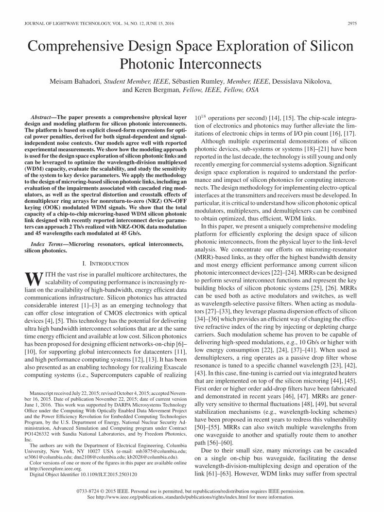
Fig. 1. Chip-to-Chip silicon photonic interconnect with an MRR-based WDM link. The optical interface of the transmitter chip includes MRR modulators thatact upon carrier dispersion principle for high speed modulation. The optical interface at the receiver includes Demux filters, photodetectors, and electronic decisioncircuitry (Det: detector). Wall-plug efficiency corresponds to the electrical to optical power conversion of the laser.
degradationof channels and inter-channel crosstalk [64]–[72].These impairments eventually put an upper limit on both themodulation speed of each channel and on the number of chan-nels, thus placing an upper bound on the maximum aggregaterate of the link [73], [74].
In this paper, we present the design and modeling platformfor obtaining the maximum achievable aggregate bandwidth in ashort-distance silicon photonic link with microring modulatorsand filters. This is achieved by estimating the effects of theinduced impairments and translating them into power penalties,i.e., an amount of extra optical power that permits compensationfor the effects of such impairments on the bit-error-ratio (BER)performance of the system [75]–[79]. We also show how thespectral statistics of a modulated light changes when it goesthrough a ring demultiplexer and how that can be turned intopower penalty.
The rest of this paper is organized as follows: in Section II,we set forth our approach in analyzing the optical power budgetof a silicon photonic link and provide a brief review of the mostimportant characteristics of non-return-to-zero ON–OFF key-ing (NRZ-OOK) modulation and estimation of BER-associatedpower penalties. The analysis is based on how the statistics of theoptical signal changes as it undergoes modulation and filtering.Sections III and IV provide details of the power penalties associ-ated with ring modulators and demultiplexers. Several availableexperimental measurements of power penalties are presented toback-up theoretical estimations. In Section V, we present ourdiscussion of optimizing the ring parameters in order to achieveminimum power penalty throughout the MRR-based link. InSection VI, the link analysis is given for a realistic power bud-get. Finally, conclusion is drawn in Section VII. Two appendicesare also provided with details of obtaining equations presentedin the paper for microring demultiplexers.
II. DESCRIPTION OF THE APPROACH
A. Optical Power Budget and Power Penalties
Consider a simple chip-to-chip silicon photonic link as shownin Fig. 1. On the transmitter side, cascaded microrings along anon-chip waveguide modulate the incoming multi-wavelengthlight generated by a comb laser source [80]. The incoming wave-lengths, once imprinted with data, are then transmitted throughan optical fiber to a receiver chip. The receiver chip consists
of multiple passive microrings whose resonances are tuned tochannel wavelengths. The total capacity of this link is obtainedby multiplying the number of channels (wavelengths) with themodulation bit rate. Intuitively, it is tempting to maximize thenumber of wavelengths, and/or to choose higher bit rates foreach channel. This allows for higher utilization of the availablespectrum in the transmission media. However, as either the num-ber of wavelengths and/or the bit rate grows, crosstalk and otherundesired impairments emerge and eventually prevent reliabletransmission. The total capacity of the link is closely tied to theoptical power losses and impairments that the light experiencesover the entire link. Summing up all the power penalties of thelink, PPdB, for a single channel, the following inequality musthold [81]:
[PdBm
laser − 10 log10(Nλ)]− PdBm
sensitivity ≥ PPdBtot . (1)
In general, aggregated optical power Plaser (sum over all wave-lengths) must stay below the nonlinear threshold of the siliconwaveguides at any point of the link [70], [74]. In contrast, thesignal powers should stay above the sensitivity of the detec-tors Psensitivity (minimum number of photons or equivalently acertain amount of optical power) at the receive side. A typical re-ceiver may have a sensitivity of −12.7 dBm at 8 Gb/s operation[77], while a good receiver may exhibit a sensitivity of about−21 dBm at 10 Gb/s [75]. The difference between lower andhigher thresholds results in the maximum power budget that canbe exploited. This budget accounts for the power penalty perchannel (how much higher should the signal hit the detector)PPtot, and for the product over the Nλ channels. We will showthat the power impairments induced by the rings depend on thespacing between channels, which is inversely proportional tothe number of wavelengths, and on the modulation rate rb . Eq.(1) is therefore a nonlinear function of Nλ and rb , and deter-mination of the Nλ × rb product that maximizes the bandwidthdirectly from it is intractable. It is however possible to optimizethe link, i.e., optimize its constituting devices, such that PPtot isminimized for different (Nλ , rb ) combinations. We proceed todo this optimization for NRZ-OOK modulation format.
B. Properties of the NRZ-OOK Modulation Format
In an NRZ-OOK modulation, the electrical signal is a se-quence of logical 0’s and 1’s that are imprinted on the envelope ofthe light. Therefore, the envelope electric field of the modulated
BAHADORI et al.: COMPREHENSIVE DESIGN SPACE EXPLORATION OF SILICON PHOTONIC INTERCONNECTS 2977
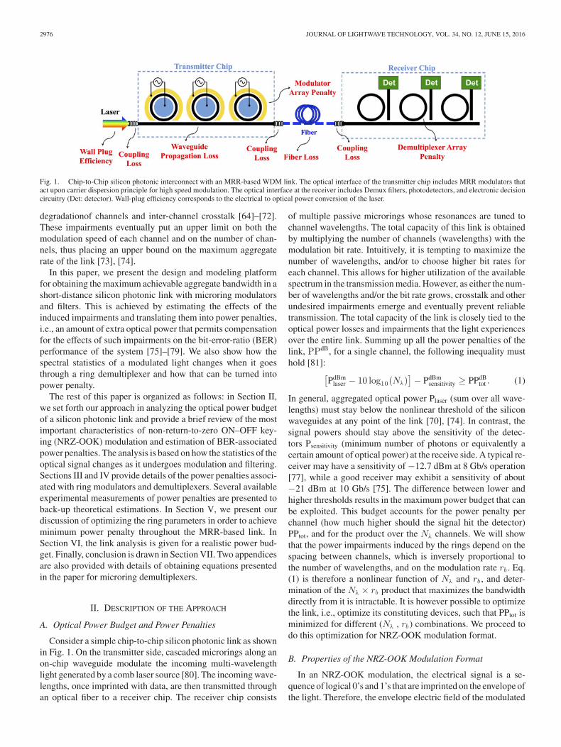
Fig. 2. Envelope electric field of the (a) NRZ-OOK modulation, and its (b)power spectral density. ER is the ratio of the optical power of the high level tothe optical power of the low level of the electric field.
light has a form of
E(t) =∞∑
k=−∞ak p(t − kTb) (2)
where Tb is the bit interval and its inverse (rb = 1/Tb ) is the bitrate of the modulation, ak is the amplitude for 0’s and 1’s bits,and p(t) is the ideal square pulse of unit amplitude and durationTb . A picture of such envelope is shown in Fig. 2(a), where thehigh level is denoted by A and the low level is denoted by B.Ideally, if the modulation has an infinite extinction ratio (ER),then the low level must be zero (B = 0); however, in practicering modulators produce a limited ER. Typical numbers for 10 Gdevices are 8–10 dB of extinction [24]. It is a practical assump-tion that all bits are equiprobable and the source of informationthat generates these bits is a stationary ergodic source. ThereforeProb(ak = A) = 0.5 and Prob(ak = B) = 0.5.
The average behavior, i.e., statistics, of such modulation isgiven by the autocorrelation of the envelope electric field overtime. The average power spectral density of the envelope ofmodulation is then the Fourier transform of its autocorrelation,which simplifies to the following equation [82], [83]:
SE (f) = μ2 δ(f − fc) + σ2 1rb
sinc2((f − fc)/rb), (3)
where
μ =A + B
2, (4a)
σ =A − B
2(4b)
fc is the optical frequency of the light, and δ(f − fc) is theDirac delta function centered at carrier frequency fc . A plotof this spectrum is presented in Fig. 2(b). The power of themodulated signal is given by integrating Eq. (3) over all fre-quencies, yielding Pav = μ2 + σ2 . We note that the power of theNRZ-OOK modulation can be decomposed based on the meanand variance of the envelope electric field. The μ2 power is atthe center frequency (represented by the delta function) and thepower of the variance (σ2) is spread over a spectrum of frequen-cies (represented by the sinc function). We will leverage Eq. (3)to estimate the power penalty of each optical component alongthe link.
C. Power Penalty Evaluation Based on Signal Statistics
As the modulated light goes through the waveguides, trans-mission medium, and other optical devices, the quality of thesignal degrades. To evaluate the breadth of the degradation, oneapproach consists of evaluating the new high and low levels(assumed to be A′ and B′) when the light reaches the receiver.Alternatively, one can analyze how the power spectral densityexperiences distortion due to the non-ideal frequency responseof the link. In other terms, one can evaluate how μ and σ evolveinto μ′ and σ′. Once these latter values are known, the powerpenalty associated with the distortion can be derived using oneof the two following models widely used in literature. If thereceiver is limited by a signal-independent noise (SIN) mech-anism (such as thermal noise) that does not beat against theoptical signal, and considering a Gaussian distribution for theuncertainty of high and low levels, the power penalty to get thesame BER performance and compensate for the signal degrada-tions is estimated as [84]
PPSIN ≈ −10 log10
(σ′
σ
μ′
μ
). (5)
In contrast, in amplified systems the noise is mainly due tothe amplified spontaneous emission (ASE) and that depends onthe intensity of the input light to the amplifier (signal dependentnoise, SDN). Using the model proposed by Downie [85] thatrelates the variance of the noise to the high and low levels of theelectric field, the power penalty is estimated as
PPSDN ≈{−10 log10 (μ′/μ) , if σ′/μ′ > 1
−10 log10 (σ′/σ) , if σ′/μ′ ≤ 1.(6)
This equation implies that the power penalty in this case is re-lated to the worst-case decrease of μ or σ. If the center frequencyloses more power than the spectral frequencies, then σ′/μ′ > 1and the power penalty is due to the change in μ. If the spectrumloses more power than the center frequency, then σ′/μ′ < 1,and the penalty is due to the change in σ. In accordance withEq. (5) and (6), two approaches can be taken to obtain powerpenalties: 1) Estimate the high and low levels (A′ and B′) first,and then find μ′ and σ′ using equations (4a) and (4b). This isthe approach we take for characterizing penalties of ring mod-ulators. 2) Directly estimate μ′ and σ′ based on μ, σ, and thefrequency response of the optical device. This is the approachwe take for the demultiplexing ring filters.
Also note that in this paper, we mainly work with SIN modeland assume no amplification in the link. If amplification is to beconsidered in the receiver, as it is the case in the experimentsagainst which this work has been compared, Eq. (6) should beemployed instead of Eq. (5).
III. MICRORING MODULATORS
MRRs are capable of modulating light at very high speedswhile operating at low powers. This property combined withthe small footprint of these optical modulators turn them intovery promising candidates for integrated photonics. The physicsbehind the operation of such modulators has been well estab-
2978 JOURNAL OF LIGHTWAVE TECHNOLOGY, VOL. 34, NO. 12, JUNE 15, 2016
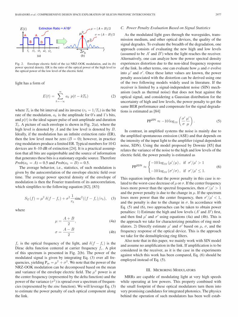
Fig. 3. (a) Schematic view of a microring modulator. The high-speed elec-trical signal is applied to the p-n-junction embedded inside the silicon ring.(b) Modulation of the input laser by shifting the resonance of the ring to createhigh and low levels of optical power at the output. (c) Graphical view of how ONand OFF states of the light at the output happen. (d) Time-domain presentationof a non-ideal NRZ OOK modulation.
lished [30]. Just like all other practical modulators, microringsare not capable of providing ideal modulation and thus someimpairments and penalties on the optical signal are inevitable.In this section, we provide a general description of the powerpenalties that are of the most importance.
As depicted in Fig. 3, the electric field envelope of the un-modulated input light has constant amplitude that we denoteby A, and constant power Pin = A2 . The modulation actionoccurs by shifting of the resonance of the ring as shown inFig. 3(b). An ideal NRZ-OOK ring modulator traps the inputlight depending on whether the data bit is “1” or “0” (shownin Fig. 3(c)). The mean and variance of this ideal modulation(from equations (4a) and (4b)) is μ = A/2, and σ = A/2, whichgives the average power Pmod = μ2 + σ2 = A2/2 = Pin/2. Wenote that −10 log10(Pmod/Pin) = 3 dB. As data bits are assumedequiprobable, this means obfuscating half of the power.
A non-ideal modulation differs from the ideal modulation inthe way that the high level is A′ instead of A (A′ < A) andthe low level is B′ instead of zero, so that P′
mod = μ′2 + σ′2 =(A′2 + B′2)/2 as plotted in Fig. 3(d). This causes the powerpenalty to grow beyond the 3 dB of an ideal modulation. Ifthe transmission of the ring for bit “0” and “1” at the laserwavelength is denoted by T0 and T1 , then A′ =
√T1 and B′ =√
T0 . T0 and T1 can be estimated by considering a Lorentzianshape for the resonance spectrum of the ring [73]. The ER ofmodulation is the ratio of power of bit “1” to the power of bit“0”, i.e., r = A′2/B′2 . Using equations (4a) and (4b) again, themean and variance of the non-ideal modulation levels can bewritten as μ′ = B′(
√r + 1)/2, and σ′ = B′(
√r − 1)/2. After
some further algebraic manipulations1 the following relationsare obtained:
μ′
μ=
√r + 1√r + 1
√P ′
mod
Pmod,
σ′
σ=
√r − 1√r + 1
√P ′
mod
Pmod. (7)
1In particular, by rewriting levels in terms of average modulation powers A
=√
2Pmod and B ′ =√
2P′mod/(r + 1).
These can be inserted into Eq. (5) or (6), depending on thenoise conditions. Considering a dominant SIN in the system, soEq. (5), the total modulation power penalty is given by
PPSINMod ≈ −10 log10
(r − 1r + 1
P ′mod
Pmod
)− 10 log10
(Pmod
Pin
)(8)
where the second term is the −3 dB corresponding to the idealmodulation. By eliminating Pmod and noting that P′
mod = (r +1)A′2/2r, the power penalty can be rewritten as
PPSINMod ≈ −10 log10
(r−1r+1
)−10 log10
(A′2
Pin
)
−10 log10
(r+12r
). (9)
This formulation is helpful as it permits to distinguish threecontributing power penalty factors. The first term is the powerpenalty due to the finite ER of modulation as widely used inthe literature [30]. The second term is the modulator insertionloss (IL), defined as the difference between the input power andthe power of bit “1.” Finally, the third term is the penalty dueto the OOK nature of the imperfect modulation. For an idealmodulator (infinite ER and no loss), this last term is 3 dB whilethe first two terms are reduced to zero.
If a silicon photonic link is dominated by the ASE noise thatbeats against the optical signal, the power penalty of modulatoris estimated from Eq. (6) by noticing that (μ′/μ)>(σ′/σ). Theresult is
PPSDNMod ≈ −10 log10
(√r − 1√r + 1
)− 5 log10
(P ′
mod
2Pin
). (10)
The first term in this equation is the power penalty due to thefinite ER of modulation (which is different from the one in Eq.(9)) and the second term represents the average power loss dueto the combination of OOK and IL of modulator.
Now, we consider several ring modulators mounted on a sili-con waveguide, each one modulating a specific wavelength (asin Fig. 1). Cascading all the ring modulators on a single buswaveguide induces two additional power penalties. The firstone to be accounted for is the passive cumulative IL of the laserpower of each channel as it passes by other rings. If the spacingbetween wavelengths is small and the number of modulators islarge, this could become a significant loss. The second one isthe array-induced multiplexing crosstalk [86]. Multiple wave-lengths of the comb laser pass by each ring, but only one of themgets modulated. Due to the carrier injection or depletion of thep-n junction of the ring, the spectrum of the ring is switched be-tween two resonance frequencies as shown in the inset of Fig. 4:f0 (OFF state) and f1 (ON state), where f1 > f0 (blue shift).If this shift (Δf = f1 − f0) is too large, then the shifted spec-trum may capture some of the power of the neighboring chan-nel that passes by the ring, hence inducing an intermodulationcrosstalk. If fΔ represents the channel spacing and fΔ > 0, thena neighboring channel at f0 + fΔ would suffer higher crosstalkthan a neighboring channel at f0 − fΔ . This leads to write the
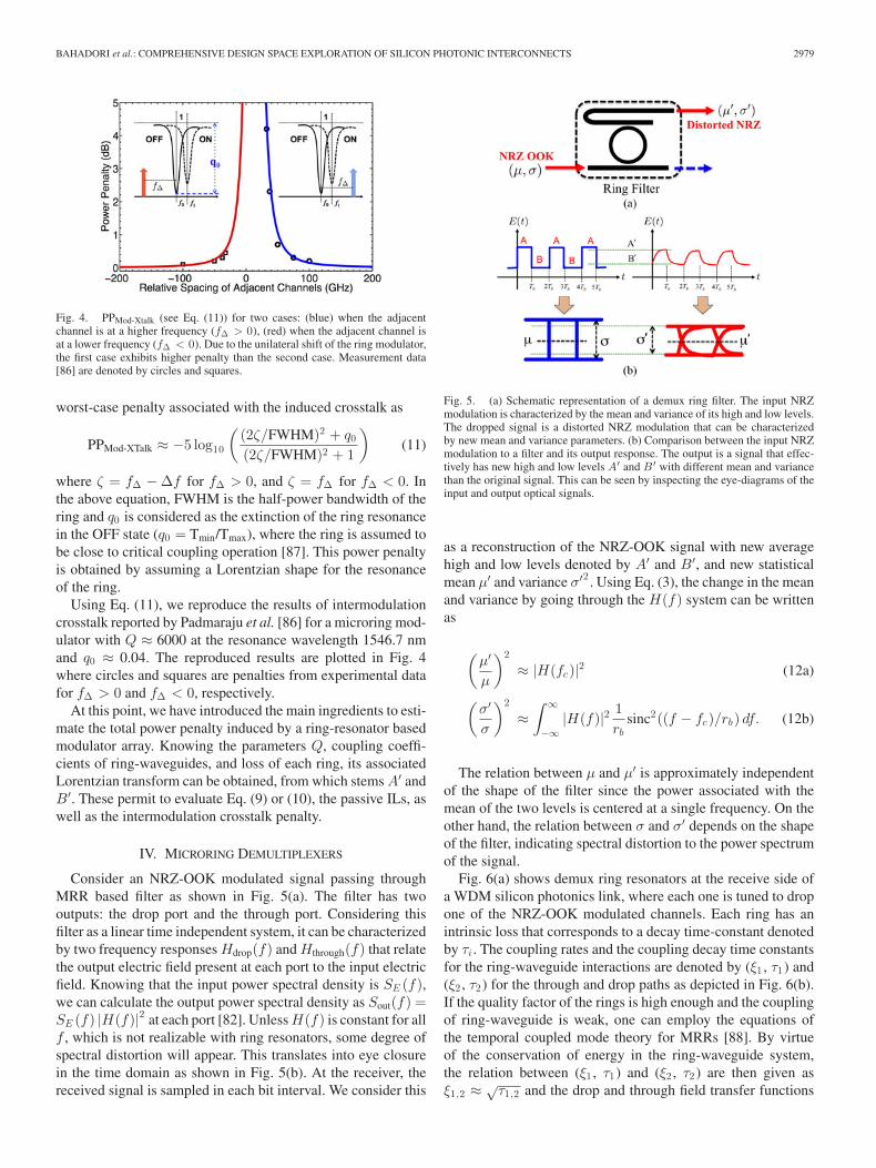
BAHADORI et al.: COMPREHENSIVE DESIGN SPACE EXPLORATION OF SILICON PHOTONIC INTERCONNECTS 2979
Fig. 4. PPMod-Xtalk (see Eq. (11)) for two cases: (blue) when the adjacentchannel is at a higher frequency (fΔ > 0), (red) when the adjacent channel isat a lower frequency (fΔ < 0). Due to the unilateral shift of the ring modulator,the first case exhibits higher penalty than the second case. Measurement data[86] are denoted by circles and squares.
worst-case penalty associated with the induced crosstalk as
PPMod-XTalk ≈ −5 log10
((2ζ/FWHM)2 + q0
(2ζ/FWHM)2 + 1
)(11)
where ζ = fΔ − Δf for fΔ > 0, and ζ = fΔ for fΔ < 0. Inthe above equation, FWHM is the half-power bandwidth of thering and q0 is considered as the extinction of the ring resonancein the OFF state (q0 = Tmin/Tmax), where the ring is assumed tobe close to critical coupling operation [87]. This power penaltyis obtained by assuming a Lorentzian shape for the resonanceof the ring.
Using Eq. (11), we reproduce the results of intermodulationcrosstalk reported by Padmaraju et al. [86] for a microring mod-ulator with Q ≈ 6000 at the resonance wavelength 1546.7 nmand q0 ≈ 0.04. The reproduced results are plotted in Fig. 4where circles and squares are penalties from experimental datafor fΔ > 0 and fΔ < 0, respectively.
At this point, we have introduced the main ingredients to esti-mate the total power penalty induced by a ring-resonator basedmodulator array. Knowing the parameters Q, coupling coeffi-cients of ring-waveguides, and loss of each ring, its associatedLorentzian transform can be obtained, from which stems A′ andB′. These permit to evaluate Eq. (9) or (10), the passive ILs, aswell as the intermodulation crosstalk penalty.
IV. MICRORING DEMULTIPLEXERS
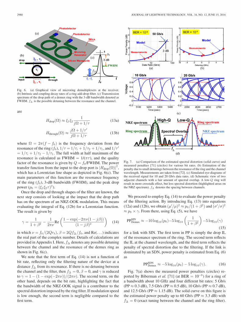
Consider an NRZ-OOK modulated signal passing throughMRR based filter as shown in Fig. 5(a). The filter has twooutputs: the drop port and the through port. Considering thisfilter as a linear time independent system, it can be characterizedby two frequency responses Hdrop(f) and Hthrough(f) that relatethe output electric field present at each port to the input electricfield. Knowing that the input power spectral density is SE (f),we can calculate the output power spectral density as Sout(f) =SE (f) |H(f)|2 at each port [82]. Unless H(f) is constant for allf , which is not realizable with ring resonators, some degree ofspectral distortion will appear. This translates into eye closurein the time domain as shown in Fig. 5(b). At the receiver, thereceived signal is sampled in each bit interval. We consider this
Fig. 5. (a) Schematic representation of a demux ring filter. The input NRZmodulation is characterized by the mean and variance of its high and low levels.The dropped signal is a distorted NRZ modulation that can be characterizedby new mean and variance parameters. (b) Comparison between the input NRZmodulation to a filter and its output response. The output is a signal that effec-tively has new high and low levels A′ and B ′ with different mean and variancethan the original signal. This can be seen by inspecting the eye-diagrams of theinput and output optical signals.
as a reconstruction of the NRZ-OOK signal with new averagehigh and low levels denoted by A′ and B′, and new statisticalmean μ′ and variance σ′2 . Using Eq. (3), the change in the meanand variance by going through the H(f) system can be writtenas
(μ′
μ
)2
≈ |H(fc)|2 (12a)
(σ′
σ
)2
≈∫ ∞
−∞|H(f)|2 1
rbsinc2((f − fc)/rb) df. (12b)
The relation between μ and μ′ is approximately independentof the shape of the filter since the power associated with themean of the two levels is centered at a single frequency. On theother hand, the relation between σ and σ′ depends on the shapeof the filter, indicating spectral distortion to the power spectrumof the signal.
Fig. 6(a) shows demux ring resonators at the receive side ofa WDM silicon photonics link, where each one is tuned to dropone of the NRZ-OOK modulated channels. Each ring has anintrinsic loss that corresponds to a decay time-constant denotedby τi . The coupling rates and the coupling decay time constantsfor the ring-waveguide interactions are denoted by (ξ1 , τ1) and(ξ2 , τ2) for the through and drop paths as depicted in Fig. 6(b).If the quality factor of the rings is high enough and the couplingof ring-waveguide is weak, one can employ the equations ofthe temporal coupled mode theory for MRRs [88]. By virtueof the conservation of energy in the ring-waveguide system,the relation between (ξ1 , τ1) and (ξ2 , τ2) are then given asξ1,2 ≈ √
τ1,2 and the drop and through field transfer functions
2980 JOURNAL OF LIGHTWAVE TECHNOLOGY, VOL. 34, NO. 12, JUNE 15, 2016
Fig. 6. (a) Graphical view of microring demultiplexers at the receiver.(b) Intrinsic and coupling decay rates of a ring add-drop filter. (c) Transmissionspectrum of the drop path of a demux ring with the 3-dB bandwidth denoted asFWHM. fΔ is the possible detuning between the resonance and the channel.
are
Hdrop(Ω) ≈ ξ1ξ21
jΩ + 1/τ(13a)
Hthrough(Ω) ≈ jΩ + 1/τ ′
jΩ + 1/τ(13b)
where Ω = 2π(f − f0) is the frequency deviation from theresonance of the ring (f0), 1/τ = 1/τi + 1/τ2 + 1/τ1 , and 1/τ ′
= 1/τi + 1/τ2 − 1/τ1 . The full width at half maximum of theresonance is calculated as FWHM = 1/(πτ ), and the qualityfactor of the resonance is given by Q = f0 /FWHM. The powertransfer function from the input to the drop port is |Hdrop(Ω)|2 ,which has a Lorentzian line shape as depicted in Fig. 6(c). Themain parameters of this function are the resonance frequencyof the ring (f0), 3-dB bandwidth (FWHM), and the peak droppower (p0 = (ξ1ξ2τ)2).
Once the drop and through shapes of the filter are known, thenext step consists of looking at the impact that the drop pathhas on the spectrum of an NRZ-OOK modulation. This meansevaluating the integral of Eq. (12b) for a Lorentzian function.The result is given by
γ =1
1 + β2 − 12πν
Re
(1 − exp(−2πν(1 − jβ))
(1 − jβ)2
)(14)
in which ν = f0/(2Qrb), β = 2QfΔ/f0 , and Re(. . . ) indicatesthe real part of the complex number. Details of calculations areprovided in Appendix I. Here, fΔ denotes any possible detuningbetween the channel and the resonance of the demux ring asshown in Fig. 6(c).
We note that the first term of Eq. (14) is not a function ofbit rate, reflecting only the filtering nature of the device at adistance fΔ from its resonance. If there is no detuning betweenthe channel and the filter, then fΔ = 0, β = 0, and γ is reducedto γ = 1 − (1 − exp(−2πν))/(2πν). The second term, on theother hand, depends on the bit rate, highlighting the fact thatthe bandwidth of the NRZ-OOK signal is a contributor to thespectral distortion imposed by the ring filter. If modulation speedis low enough, the second term is negligible compared to thefirst term.
Fig. 7. (a) Comparison of the estimated spectral distortion (solid curve) andmeasured penalties [71] (circles) for various bit rates. (b) Estimation of thepenalty due to small detunings between the resonance of the ring and the channelwavelength. Measurements are taken from [72]. (c) Simulated eye-diagrams ofthe received signal for 10 and 20 Gb/s data rates. (d) Schematic view of twoadjacent channels with a fair amount of spectral overlap. A low-Q ring willresult in more crosstalk effect, but less spectral distortion (highlighted areas onthe NRZ spectrum). fΔ denotes the spacing between channels.
We proceed to employ Eq. (14) to evaluate the power penaltyof the filtering action. By introducing Eq. (13) into equations(12a) and (12b), we obtain (μ′/μ)2 ≈ p0/(1 + β2) and (σ′/σ)2
≈ p0 × γ. From there, using Eq. (5), we have
PPSINDemux ≈ −10 log10(p0)−5 log10
(1
1 + β2
)−5 log10(γ)
(15)for a link with SIN. The first term in PP is simply the drop ILof the resonance spectrum of the ring. The second term reflectsthe IL at the channel wavelength, and the third term reflects thepenalty of spectral distortion due to the filtering. If the link isdominated by an SDN, power penalty is estimated from Eq. (6)as
PPSDNDemux ≈ −5 log10(p0) − 5 log10(γ). (16)
Fig. 7(a) shows the measured power penalties (circles) re-ported by Biberman et al. [71] (at BER = 10−9) for a ring ofa bandwidth about 10 GHz and four different bit rates: 5 Gb/s(PP ≈ 0.3 dB), 7.5 Gb/s (PP ≈ 0.5 dB), 10 Gb/s (PP ≈ 0.7 dB),and 12.5 Gb/s (PP ≈ 1.15 dB). The solid curve on this figure isthe estimated power penalty up to 60 Gb/s (PP ≈ 3.3 dB) withfΔ = 0 (exact tuning between the channel and the ring filter).
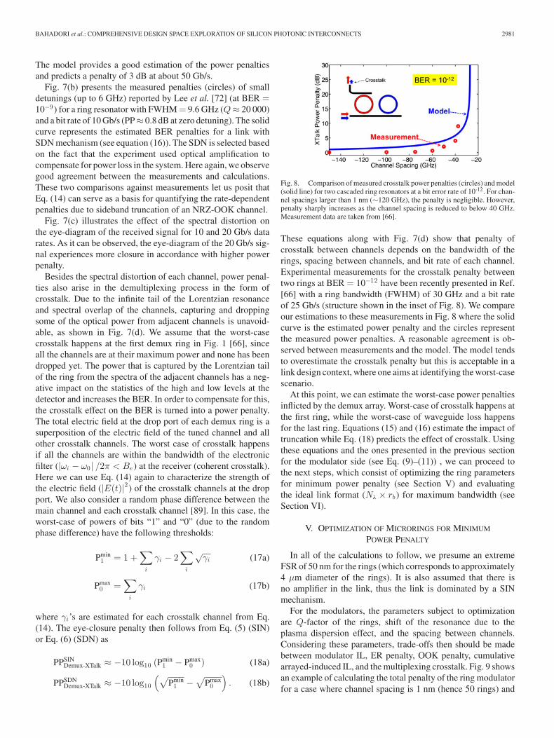
BAHADORI et al.: COMPREHENSIVE DESIGN SPACE EXPLORATION OF SILICON PHOTONIC INTERCONNECTS 2981
The model provides a good estimation of the power penaltiesand predicts a penalty of 3 dB at about 50 Gb/s.
Fig. 7(b) presents the measured penalties (circles) of smalldetunings (up to 6 GHz) reported by Lee et al. [72] (at BER =10−9) for a ring resonator with FWHM = 9.6 GHz (Q≈ 20 000)and a bit rate of 10 Gb/s (PP≈ 0.8 dB at zero detuning). The solidcurve represents the estimated BER penalties for a link withSDN mechanism (see equation (16)). The SDN is selected basedon the fact that the experiment used optical amplification tocompensate for power loss in the system. Here again, we observegood agreement between the measurements and calculations.These two comparisons against measurements let us posit thatEq. (14) can serve as a basis for quantifying the rate-dependentpenalties due to sideband truncation of an NRZ-OOK channel.
Fig. 7(c) illustrates the effect of the spectral distortion onthe eye-diagram of the received signal for 10 and 20 Gb/s datarates. As it can be observed, the eye-diagram of the 20 Gb/s sig-nal experiences more closure in accordance with higher powerpenalty.
Besides the spectral distortion of each channel, power penal-ties also arise in the demultiplexing process in the form ofcrosstalk. Due to the infinite tail of the Lorentzian resonanceand spectral overlap of the channels, capturing and droppingsome of the optical power from adjacent channels is unavoid-able, as shown in Fig. 7(d). We assume that the worst-casecrosstalk happens at the first demux ring in Fig. 1 [66], sinceall the channels are at their maximum power and none has beendropped yet. The power that is captured by the Lorentzian tailof the ring from the spectra of the adjacent channels has a neg-ative impact on the statistics of the high and low levels at thedetector and increases the BER. In order to compensate for this,the crosstalk effect on the BER is turned into a power penalty.The total electric field at the drop port of each demux ring is asuperposition of the electric field of the tuned channel and allother crosstalk channels. The worst case of crosstalk happensif all the channels are within the bandwidth of the electronicfilter (|ωi − ω0 | /2π < Be ) at the receiver (coherent crosstalk).Here we can use Eq. (14) again to characterize the strength ofthe electric field (|E(t)|2) of the crosstalk channels at the dropport. We also consider a random phase difference between themain channel and each crosstalk channel [89]. In this case, theworst-case of powers of bits “1” and “0” (due to the randomphase difference) have the following thresholds:
Pmin1 = 1 +
∑
i
γi − 2∑
i
√γi (17a)
Pmax0 =
∑
i
γi (17b)
where γi’s are estimated for each crosstalk channel from Eq.(14). The eye-closure penalty then follows from Eq. (5) (SIN)or Eq. (6) (SDN) as
PPSINDemux-XTalk ≈ −10 log10 (Pmin
1 − Pmax0 ) (18a)
PPSDNDemux-XTalk ≈ −10 log10
(√Pmin
1 −√
Pmax0
). (18b)
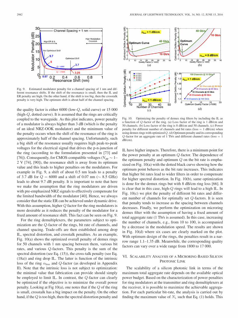
Fig. 8. Comparison of measured crosstalk power penalties (circles) and model(solid line) for two cascaded ring resonators at a bit error rate of 10-12. For chan-nel spacings larger than 1 nm (∼120 GHz), the penalty is negligible. However,penalty sharply increases as the channel spacing is reduced to below 40 GHz.Measurement data are taken from [66].
These equations along with Fig. 7(d) show that penalty ofcrosstalk between channels depends on the bandwidth of therings, spacing between channels, and bit rate of each channel.Experimental measurements for the crosstalk penalty betweentwo rings at BER = 10−12 have been recently presented in Ref.[66] with a ring bandwidth (FWHM) of 30 GHz and a bit rateof 25 Gb/s (structure shown in the inset of Fig. 8). We compareour estimations to these measurements in Fig. 8 where the solidcurve is the estimated power penalty and the circles representthe measured power penalties. A reasonable agreement is ob-served between measurements and the model. The model tendsto overestimate the crosstalk penalty but this is acceptable in alink design context, where one aims at identifying the worst-casescenario.
At this point, we can estimate the worst-case power penaltiesinflicted by the demux array. Worst-case of crosstalk happens atthe first ring, while the worst-case of waveguide loss happensfor the last ring. Equations (15) and (16) estimate the impact oftruncation while Eq. (18) predicts the effect of crosstalk. Usingthese equations and the ones presented in the previous sectionfor the modulator side (see Eq. (9)–(11)) , we can proceed tothe next steps, which consist of optimizing the ring parametersfor minimum power penalty (see Section V) and evaluatingthe ideal link format (Nλ × rb ) for maximum bandwidth (seeSection VI).
V. OPTIMIZATION OF MICRORINGS FOR MINIMUM
POWER PENALTY
In all of the calculations to follow, we presume an extremeFSR of 50 nm for the rings (which corresponds to approximately4 μm diameter of the rings). It is also assumed that there isno amplifier in the link, thus the link is dominated by a SINmechanism.
For the modulators, the parameters subject to optimizationare Q-factor of the rings, shift of the resonance due to theplasma dispersion effect, and the spacing between channels.Considering these parameters, trade-offs then should be madebetween modulator IL, ER penalty, OOK penalty, cumulativearrayed-induced IL, and the multiplexing crosstalk. Fig. 9 showsan example of calculating the total penalty of the ring modulatorfor a case where channel spacing is 1 nm (hence 50 rings) and
2982 JOURNAL OF LIGHTWAVE TECHNOLOGY, VOL. 34, NO. 12, JUNE 15, 2016
Fig. 9. Estimated modulator penalty for a channel spacing of 1 nm and dif-ferent resonance shifts. If the shift of the resonance is small, then the IL andER penalty are high. On the other hand, if the shift is too big, then the crosstalkpenalty is very high. The optimum shift is about half of the channel spacing.
the quality factor is either 6000 (low-Q, solid curve) or 15 000(high-Q, dotted curve). It is assumed that the rings are criticallycoupled to the waveguide. As this plot indicates, power penaltyof a modulator is always higher than 3 dB (which is the penaltyof an ideal NRZ-OOK modulator) and the minimum value ofthe penalty occurs when the shift of the resonance of the ring isapproximately half of the channel spacing. Unfortunately, sucha big shift of the resonance usually requires high peak-to-peakvoltages for the electrical signal that drives the p-n-junction ofthe ring (according to the formulation presented in [73] and[76]). Consequently, for CMOS-compatible voltages (Vpp ∼ 1–2 V [74], [90]), the resonance shift is away from its optimumvalue and this leads to higher penalties on the modulators. Forexample in Fig. 9, a shift of about 0.5 nm leads to a penaltyof 3.7 dB for Q = 6000 and a shift of 0.07 nm (∼ 8.5 GHz)leads to about 9.7 dB penalty. It is important to note that herewe make the assumption that the ring modulators are drivenwith pre-emphasized NRZ signals to effectively compensate forthe limited bandwidth of the modulator [40]. Hence, we alwaysconsider that the static ER can be achieved under dynamic drive.With this assumption, higher Q factor for the ring modulators ismore desirable as it reduces the penalty of the modulator for afixed amount of resonance shift. This fact can be seen on Fig. 9.
For the ring demultiplexers, the parameters subject to opti-mization are the Q-factor of the rings, bit rate of channels, andchannel spacing. Trade-offs are then established among dropIL, spectral distortion, and crosstalk penalties. As an example,Fig. 10(a) shows the optimized overall penalty of demux ringsfor 50 channels with 1 nm spacing between them, various bitrates, and various Q-factors. This penalty is the sum of thespectral distortion (see Eq. (15)), the cross-talk penalty (see Eq.(18a)) and ring drop IL. The latter is function of the intrinsicloss of the ring αloss and Q-factor (as developed in AppendixII). Note that the intrinsic loss is not subject to optimization:the minimal value that fabrication can provide should simplybe employed to limit IL. In contrast, the Q-factor can clearlybe optimized if the objective is to minimize the overall powerpenalty. Looking at Fig 10(a), one notes that if the Q of the ringis small, crosstalk has a big impact on the penalty. On the otherhand, if the Q is too high, then the spectral distortion penalty and
Fig. 10. Optimizing the penalty of demux ring filters by including the IL asa function of Q-factor of the ring. (a) Loss factor of the ring is 1 dB/cm and50 channels. (b) Loss factor of the ring is 8 dB/cm and 50 channels. (c) Powerpenalty for different number of channels and bit rates (loss = 1 dB/cm) whenusing demux rings with optimized Q. (d) Optimum penalty and its correspondingQ-factor for an aggregate rate of 1 Tb/s and different channel rates (loss = 1dB/cm).
IL have higher impacts. Therefore, there is a minimum point forthe power penalty at an optimum Q-factor. The dependence ofthe optimum penalty and optimum Q on the bit rate is empha-sized on Fig. 10(a) with the dotted black curve showing how theoptimum point behaves as the bit rate increases. This indicatesthat higher bit rates lead to wider filters in order to compensatefor higher spectral distortion. In Fig. 10(b), same optimizationis done for the demux rings but with 8 dB/cm ring loss [66]. Itis clear that in this case, high-Q rings will lead to a high IL. InFig. 10(c) we plot the penalty of different bit rates and differ-ent number of channels for optimally set Q-factors. It is seenthat penalty tends to increase as the spacing between channelsdecreases. Finally, we perform the optimization on microringdemux filter with the assumption of having a fixed amount oftotal aggregate rate (1 Tb/s is assumed). In this case, increasingthe number of channels, e.g., from 10 to 100, is accompaniedby a decrease in the modulation speed. The results are shownin Fig. 10(d) where six cases are clearly marked on the plot.With optimum design of the rings, the penalties result in a nar-row range 1.1–1.35 dB. Meanwhile, the corresponding qualityfactors can vary over a wide range from 1800 to 17 000.
VI. SCALABILITY ANALYSIS OF A MICRORING-BASED SILICON
PHOTONIC LINK
The scalability of a silicon photonic link in terms of themaximum total aggregate rate depends on the available opticalpower budget. Based on the characterization of power penaltiesfor ring modulators at the transmitter and ring demultiplexers atthe receiver, it is possible to maximize the achievable aggrega-tion. For each particular bit-rate, the analysis is carried out byfinding the maximum value of Nλ such that Eq. (1) holds. This

BAHADORI et al.: COMPREHENSIVE DESIGN SPACE EXPLORATION OF SILICON PHOTONIC INTERCONNECTS 2983
Fig. 11. Calculation of the available optical power at the output of the transmit-ter and minimum required power at the input of the receiver. Both calculationsreflect the worst-case. The difference is the available power budget for lossesand penalties associated with fibers, or switches that are placed between trans-mitter and receiver. The capacity of the link is estimated to be 1.2 Tb/s. Qualityfactor of ring modulators is taken to be 12 000 and intrinsic loss factor αloss tobe 1 dB/cm.
is done by incorporating power penalties from Eq. (9) or (10),(11), (15) or (16), and (18) into the PPtot term in Eq. (1). Someof the power penalties of the link do not generally depend onthe bit-rate of channels or on the number of channels/channelspacing. Examples include the waveguide propagation loss (∼1 dB/cm) and chip-to-fiber/fiber-to-chip coupling IL (∼ 1 dB)[74]. The penalties of the modulators are also approximatelyindependent of bit-rate, but depend on the number of channelsdue to array-induced IL and inter-modulation crosstalk. Thiscan be taken as an encouragement to use higher bit-rates at themodulators. However, higher bit-rates limit the sensitivity of thereceiver circuitry which, as we will see, eventually puts a capon the maximum achievable bandwidth. Overall, this engendersan interesting design space to explore.
We initiate our explorations by calculating the available powerat the output of the transmitter chip and the minimum requiredpower at the input of the receiver as a function of numberof channels for 10 Gb/s NRZ-OOK modulation, as shown inFig. 11. It is assumed that laser can provide a maximum powerof 5 dBm for each wavelength (after coupling into the wave-guide), but the total amount of the optical power that is injectedinto the silicon waveguide is kept below 20 dBm to avoid thenonlinearities of the silicon waveguide. The sensitivity of thereceiver for each channel is set to a value of −15.5 dBm (givenby a rate-dependent model, to be described later). These as-sumptions set the limit of the maximum power budget to 20.5dB for each 10 Gb/s channel. From the transmitter side, we addup the modulator penalties (loss, ER, crosstalk) and the wave-guide loss, assuming 1 dB/cm loss for the silicon waveguide.Since the number of required modulators and demultiplexers isequal to the number of channels, the length of the waveguideslinearly scales up with the number of channels. Then, we add upthe worst-case penalty associated with the demultiplexers (in-cluding worst-case crosstalk and worst-case waveguide loss).We also account for a 2 dB extra margin to compensate jitterin clocking. In contrast, we do not account for power penaltiesrelated to chromatic dispersion. We assume this last to be negli-gible for short distance links with modulation rates < 100 Gb/s.Fig. 11 shows that at about 120 channels, the power budget
Fig. 12. Estimated sensitivity of the receiver as a function of the modulationdata rate. At low data rates, dark current dominates over the noise current andthus the sensitivity is almost constant, whereas at high data rates the noisecurrent dominates over the dark current and sensitivity is reduced.
completely closes and thus the scalability of this link for 10Gb/s channels is limited to about 1.2 Tb/s. For lower number ofchannels, there is some budget remaining. It can be exploitedto introduce additional elements in the link (more couplers,switches, etc.). Alternatively, launching powers per channel canbe reduced to limit the power consumption of the laser.
Next, the dependence of the scalability of the link on themodulation speed is investigated. In this case, we still assume thesame condition on laser power (5 dBm per channel, maximum20 dBm total), but a bit-rate dependent model for the sensitivityof Germanium-based detector is employed. The model for thesensitivity is based on the simple definition of the BER forOOK modulation with Gaussian noise at the receiver. Therefore,sensitivity is defined by the following equation:
Psensitivity ≈ 10 log10
(QBER
Idark+IRMSnoise
R
10ER/10+110ER/10−1
)(19)
where QBER is the argument of the complementary error function(QBER = 7 for BER = 10−12), R is a responsivity [A/W] of thephotodiode (assumed ∼0.7 A/W), ER is the extinction ratioof input signal [dB] (assumed ∼10 dB as a reference), Idark isthe dark current [mA] (assumed ∼1 μA) and Inoise is the totalRMS input-referred noise current [mA] of the receiver [19],[91]–[95]. For simplicity, we also assume that the receiver hasenough bandwidth to accommodate the designated bit rate (BW≈ 0.75 DataRate). The noise current is estimated from an input-referred RC equivalent circuit for the receiver (photodiode +TIA) whose 3 dB bandwidth is set to the bandwidth of thereceiver [19]. Fig. 12 shows a plot of the obtained sensitivity forBER = 10−12 . The sensitivity is dominated by dark current atlow data rates, whereas at high data rates is dominated by thenoise current. A sensitivity of −15.5 dBm is then obtained for10 Gb/s NRZ OOK modulation.
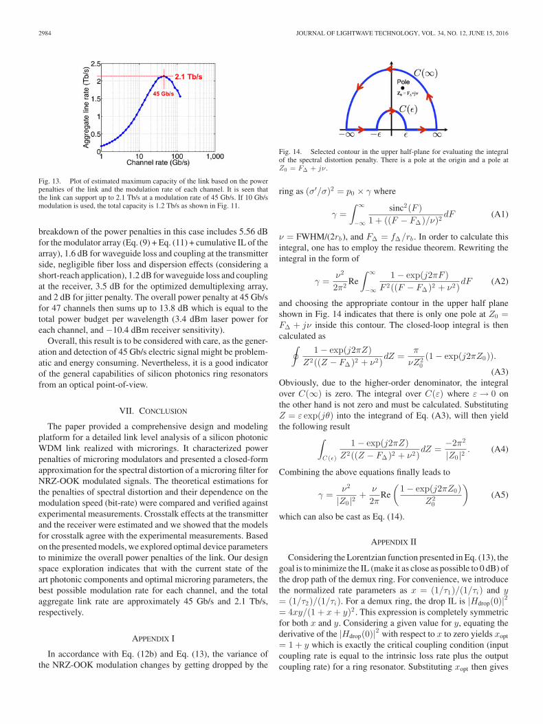
We identify the highest number of channels supported foreach modulation rate up to 120 Gb/s (see Fig. 13). By evaluatingthe link format (Nλ × rb product), it is found that a chip-to-chipsilicon photonic link, under the considered assumptions, cansupport a peak aggregated bandwidth of∼2.1 Tb/s, composed of47 channels at 45 Gb/s. This corresponds to a channel spacing of1.06 nm (i.e., ∼125 GHz) and a modulator shift of 0.53 nm. The
2984 JOURNAL OF LIGHTWAVE TECHNOLOGY, VOL. 34, NO. 12, JUNE 15, 2016
Fig. 13. Plot of estimated maximum capacity of the link based on the powerpenalties of the link and the modulation rate of each channel. It is seen thatthe link can support up to 2.1 Tb/s at a modulation rate of 45 Gb/s. If 10 Gb/smodulation is used, the total capacity is 1.2 Tb/s as shown in Fig. 11.
breakdown of the power penalties in this case includes 5.56 dBfor the modulator array (Eq. (9) + Eq. (11) + cumulative IL of thearray), 1.6 dB for waveguide loss and coupling at the transmitterside, negligible fiber loss and dispersion effects (considering ashort-reach application), 1.2 dB for waveguide loss and couplingat the receiver, 3.5 dB for the optimized demultiplexing array,and 2 dB for jitter penalty. The overall power penalty at 45 Gb/sfor 47 channels then sums up to 13.8 dB which is equal to thetotal power budget per wavelength (3.4 dBm laser power foreach channel, and −10.4 dBm receiver sensitivity).
Overall, this result is to be considered with care, as the gener-ation and detection of 45 Gb/s electric signal might be problem-atic and energy consuming. Nevertheless, it is a good indicatorof the general capabilities of silicon photonics ring resonatorsfrom an optical point-of-view.
VII. CONCLUSION
The paper provided a comprehensive design and modelingplatform for a detailed link level analysis of a silicon photonicWDM link realized with microrings. It characterized powerpenalties of microring modulators and presented a closed-formapproximation for the spectral distortion of a microring filter forNRZ-OOK modulated signals. The theoretical estimations forthe penalties of spectral distortion and their dependence on themodulation speed (bit-rate) were compared and verified againstexperimental measurements. Crosstalk effects at the transmitterand the receiver were estimated and we showed that the modelsfor crosstalk agree with the experimental measurements. Basedon the presented models, we explored optimal device parametersto minimize the overall power penalties of the link. Our designspace exploration indicates that with the current state of theart photonic components and optimal microring parameters, thebest possible modulation rate for each channel, and the totalaggregate link rate are approximately 45 Gb/s and 2.1 Tb/s,respectively.
APPENDIX I
In accordance with Eq. (12b) and Eq. (13), the variance ofthe NRZ-OOK modulation changes by getting dropped by the
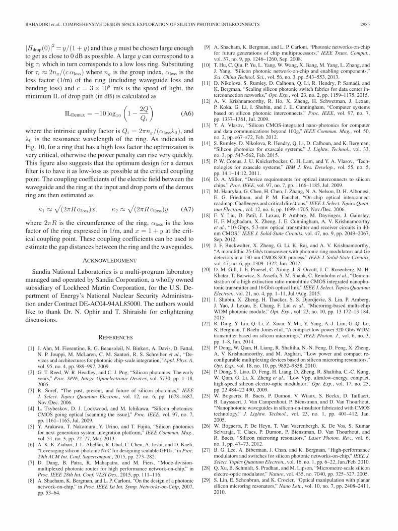
Fig. 14. Selected contour in the upper half-plane for evaluating the integralof the spectral distortion penalty. There is a pole at the origin and a pole atZ0 = FΔ + jν .
ring as (σ′/σ)2 = p0 × γ where
γ =∫ ∞
−∞
sinc2(F )1 + ((F − FΔ)/ν)2 dF (A1)
ν = FWHM/(2rb ), and FΔ = fΔ/rb . In order to calculate thisintegral, one has to employ the residue theorem. Rewriting theintegral in the form of
γ =ν2
2π2 Re∫ ∞
−∞
1 − exp(j2πF )F 2((F − FΔ)2 + ν2)
dF (A2)
and choosing the appropriate contour in the upper half planeshown in Fig. 14 indicates that there is only one pole at Z0 =FΔ + jν inside this contour. The closed-loop integral is thencalculated as
∮1 − exp(j2πZ)
Z2((Z − FΔ)2 + ν2)dZ =
π
νZ20(1 − exp(j2πZ0)).
(A3)Obviously, due to the higher-order denominator, the integralover C(∞) is zero. The integral over C(ε) where ε → 0 onthe other hand is not zero and must be calculated. SubstitutingZ = ε exp(jθ) into the integrand of Eq. (A3), will then yieldthe following result
∫
C (ε)
1 − exp(j2πZ)Z2((Z − FΔ)2 + ν2)
dZ =−2π2
|Z0 |2. (A4)
Combining the above equations finally leads to
γ =ν2
|Z0 |2+
ν
2πRe
(1 − exp(j2πZ0)
Z20
)(A5)
which can also be cast as Eq. (14).
APPENDIX II
Considering the Lorentzian function presented in Eq. (13), thegoal is to minimize the IL (make it as close as possible to 0 dB) ofthe drop path of the demux ring. For convenience, we introducethe normalized rate parameters as x = (1/τ1)/(1/τi) and y= (1/τ2)/(1/τi). For a demux ring, the drop IL is |Hdrop(0)|2= 4xy/(1 + x + y)2 . This expression is completely symmetricfor both x and y. Considering a given value for y, equating thederivative of the |Hdrop(0)|2 with respect to x to zero yields xopt
= 1 + y which is exactly the critical coupling condition (inputcoupling rate is equal to the intrinsic loss rate plus the outputcoupling rate) for a ring resonator. Substituting xopt then gives
BAHADORI et al.: COMPREHENSIVE DESIGN SPACE EXPLORATION OF SILICON PHOTONIC INTERCONNECTS 2985
|Hdrop(0)|2 = y/(1 + y) and thus y must be chosen large enoughto get as close to 0 dB as possible. A large y can correspond to abig τi which in turn corresponds to a low loss ring. Substitutingfor τi ≈ 2ng/(c αloss) where ng is the group index, αloss is theloss factor (1/m) of the ring (including waveguide loss andbending loss) and c = 3 × 10⁸ m/s is the speed of light, theminimum IL of drop path (in dB) is calculated as
ILDemux = −10 log10
(1 − 2Q
Qi
)(A6)
where the intrinsic quality factor is Qi = 2πng/(αlossλ0), andλ0 is the resonance wavelength of the ring. As indicated inFig. 10, for a ring that has a high loss factor the optimization isvery critical, otherwise the power penalty can rise very quickly.This figure also suggests that the optimum design for a demuxfilter is to have it as low-loss as possible at the critical couplingpoint. The coupling coefficients of the electric field between thewaveguide and the ring at the input and drop ports of the demuxring are then estimated as
κ1 ≈√
(2πR αloss)x, κ2 ≈√
(2πR αloss)y (A7)
where 2πR is the circumference of the ring, αloss is the lossfactor of the ring expressed in 1/m, and x = 1 + y at the crit-ical coupling point. These coupling coefficients can be used toestimate the gap distances between the ring and the waveguides.
ACKNOWLEDGMENT
Sandia National Laboratories is a multi-program laboratorymanaged and operated by Sandia Corporation, a wholly ownedsubsidiary of Lockheed Martin Corporation, for the U.S. De-partment of Energy’s National Nuclear Security Administra-tion under Contract DE-AC04-94AL85000. The authors wouldlike to thank Dr. N. Ophir and T. Shiraishi for enlighteningdiscussions.
REFERENCES
[1] J. Ahn, M. Fiorentino, R. G. Beausoleil, N. Binkert, A. Davis, D. Fattal,N. P. Jouppi, M. McLaren, C. M. Santori, R. S. Schreiber et al., “De-vices and architectures for photonic chip-scale integration,” Appl. Phys. A,vol. 95, no. 4, pp. 989–997, 2009.
[2] G. T. Reed, W. R. Headley, and C. J. Png, “Silicon photonics: The earlyyears,” Proc. SPIE, Integr. Optoelectronic Devices, vol. 5730, pp. 1–18,2005.
[3] R. Soref, “The past, present, and future of silicon photonics,” IEEEJ. Select. Topics Quantum Electron., vol. 12, no. 6, pp. 1678–1687,Nov./Dec. 2006.
[4] L. Tsybeskov, D. J. Lockwood, and M. Ichikawa, “Silicon photonics:CMOS going optical [scanning the issue],” Proc. IEEE, vol. 97, no. 7,pp. 1161–1165, Jul. 2009.
[5] Y. Arakawa, T. Nakamura, Y. Urino, and T. Fujita, “Silicon photonicsfor next generation system integration platform,” IEEE Commun. Mag.,vol. 51, no. 3, pp. 72–77, Mar. 2013.
[6] A. K. K. Ziabari, J. L. Abellan, R. Ubal, C. Chen, A. Joshi, and D. Kaeli,“Leveraging silicon-photonic NoC for designing scalable GPUs,” in Proc.29th ACM Int. Conf. Supercomput., 2015, pp. 273–282.
[7] D. Dang, B. Patra, R. Mahapatra, and M. Fiers, “Mode-division-multiplexed photonic router for high performance network-on-chip,” inProc. IEEE 28th Int. Conf. VLSI Des., 2015, pp. 111–116.
[8] A. Shacham, K. Bergman, and L. P. Carloni, “On the design of a photonicnetwork-on-chip,” in Proc. IEEE Ist Int. Symp. Networks-on-Chip, 2007,pp. 53–64.
[9] A. Shacham, K. Bergman, and L. P. Carloni, “Photonic networks-on-chipfor future generations of chip multiprocessors,” IEEE Trans. Comput.,vol. 57, no. 9, pp. 1246–1260, Sep. 2008.
[10] T. Hu, C. Qiu, P. Yu, L. Yang, W. Wang, X. Jiang, M. Yang, L. Zhang, andJ. Yang, “Silicon photonic network-on-chip and enabling components,”Sci. China Technol. Sci., vol. 56, no. 3, pp. 543–553, 2013.
[11] D. Nikolova, S. Rumley, D. Calhoun, Q. Li, R. Hendry, P. Samadi, andK. Bergman, “Scaling silicon photonic switch fabrics for data center in-terconnection networks,” Opt. Exp., vol. 23, no. 2, pp. 1159–1175, 2015.
[12] A. V. Krishnamoorthy, R. Ho, X. Zheng, H. Schwetman, J. Lexau,P. Koka, G. Li, I. Shubin, and J. E. Cunningham, “Computer systemsbased on silicon photonic interconnects,” Proc. IEEE, vol. 97, no. 7,pp. 1337–1361, Jul. 2009.
[13] Y. A. Vlasov, “Silicon CMOS-integrated nano-photonics for computerand data communications beyond 100g,” IEEE Commun. Mag., vol. 50,no. 2, pp. s67–s72, Feb. 2012.
[14] S. Rumley, D. Nikolova, R. Hendry, Q. Li, D. Calhoun, and K. Bergman,“Silicon photonics for exascale systems,” J. Lightw. Technol., vol. 33,no. 3, pp. 547–562, Feb. 2015.
[15] P. W. Coteus, J. U. Knickerbocker, C. H. Lam, and Y. A. Vlasov, “Tech-nologies for exascale systems,” IBM J. Res. Develop., vol. 55, no. 5,pp. 14:1–14:12, 2011.
[16] D. A. Miller, “Device requirements for optical interconnects to siliconchips,” Proc. IEEE, vol. 97, no. 7, pp. 1166–1185, Jul. 2009.
[17] M. Haurylau, G. Chen, H. Chen, J. Zhang, N. A. Nelson, D. H. Albonesi,E. G. Friedman, and P. M. Fauchet, “On-chip optical interconnectroadmap: Challenges and critical directions,” IEEE J. Select. Topics Quan-tum Electron., vol. 12, no. 6, pp. 1699–1705, Nov./Dec. 2006.
[18] F. Y. Liu, D. Patil, J. Lexau, P. Amberg, M. Dayringer, J. Gainsley,H. F. Moghadam, X. Zheng, J. E. Cunningham, A. V. Krishnamoorthyet al., “10-Gbps, 5.3-mw optical transmitter and receiver circuits in 40-nm CMOS,” IEEE J. Solid-State Circuits, vol. 47, no. 9, pp. 2049–2067,Sep. 2012.
[19] J. F. Buckwalter, X. Zheng, G. Li, K. Raj, and A. V. Krishnamoorthy,“A monolithic 25-Gb/s transceiver with photonic ring modulators and Gedetectors in a 130-nm CMOS SOI process,” IEEE J. Solid-State Circuits,vol. 47, no. 6, pp. 1309–1322, Jun. 2012.
[20] D. M. Gill, J. E. Proesel, C. Xiong, J. S. Orcutt, J. C. Rosenberg, M. H.Khater, T. Barwicz, S. Assefa, S. M. Shank, C. Reinholm et al., “Demon-stration of a high extinction ratio monolithic CMOS integrated nanopho-tonic transmitter and 16 Gb/s optical link,” IEEE J. Select. Topics QuantumElectron., vol. 21, no. 4, pp. 1–11, Jul./Aug. 2015.
[21] I. Shubin, X. Zheng, H. Thacker, S. S. Djordjevic, S. Lin, P. Amberg,J. Yao, J. Lexau, E. Chang, F. Liu et al., “Microring-based multi-chipWDM photonic module,” Opt. Exp., vol. 23, no. 10, pp. 13 172–13 184,2015.
[22] R. Ding, Y. Liu, Q. Li, Z. Xuan, Y. Ma, Y. Yang, A.-J. Lim, G.-Q. Lo,K. Bergman, T. Baehr-Jones et al.,“A compact low-power 320-Gb/s WDMtransmitter based on silicon microrings,” IEEE Photon. J., vol. 6, no. 3,pp. 1–8, Jun. 2014.
[23] P. Dong, W. Qian, H. Liang, R. Shafiiha, N.-N. Feng, D. Feng, X. Zheng,A. V. Krishnamoorthy, and M. Asghari, “Low power and compact re-configurable multiplexing devices based on silicon microring resonators,”Opt. Exp., vol. 18, no. 10, pp. 9852–9858, 2010.
[24] P. Dong, S. Liao, D. Feng, H. Liang, D. Zheng, R. Shafiiha, C.-C. Kung,W. Qian, G. Li, X. Zheng et al., “Low Vpp, ultralow-energy, compact,high-speed silicon electro-optic modulator,” Opt. Exp., vol. 17, no. 25,pp. 22 484–22 490, 2009.
[25] W. Bogaerts, R. Baets, P. Dumon, V. Wiaux, S. Beckx, D. Taillaert,B. Luyssaert, J. Van Campenhout, P. Bienstman, and D. Van Thourhout,“Nanophotonic waveguides in silicon-on-insulator fabricated with CMOStechnology,” J. Lightw. Technol., vol. 23, no. 1, pp. 401–412, Jan.2005.
[26] W. Bogaerts, P. De Heyn, T. Van Vaerenbergh, K. De Vos, S. KumarSelvaraja, T. Claes, P. Dumon, P. Bienstman, D. Van Thourhout, andR. Baets, “Silicon microring resonators,” Laser Photon. Rev., vol. 6,no. 1, pp. 47–73, 2012.
[27] B. G. Lee, A. Biberman, J. Chan, and K. Bergman, “High-performancemodulators and switches for silicon photonic networks-on-chip,” IEEE J.Select. Topics Quantum Electron., vol. 16, no. 1, pp. 6–22, Jan./Feb. 2010.
[28] Q. Xu, B. Schmidt, S. Pradhan, and M. Lipson, “Micrometre-scale siliconelectro-optic modulator,” Nature, vol. 435, no. 7040, pp. 325–327, 2005.
[29] S. Lin, E. Schonbrun, and K. Crozier, “Optical manipulation with planarsilicon microring resonators,” Nano Lett., vol. 10, no. 7, pp. 2408–2411,2010.
2986 JOURNAL OF LIGHTWAVE TECHNOLOGY, VOL. 34, NO. 12, JUNE 15, 2016
[30] G. Li, A. V. Krishnamoorthy, I. Shubin, J. Yao, Y. Luo, H. Thacker,X. Zheng, K. Raj, and J. E. Cunningham, “Ring resonator modulatorsin silicon for interchip photonic links,” IEEE J. Select. Topics QuantumElectron., vol. 19, no. 6, pp. 95–113, Nov./Dec. 2013.
[31] L. Zhang, Y. Li, M. Song, J.-Y. Yang, R. G. Beausoleil, and A. E. Willner,“Silicon microring-based signal modulation for chip-scale optical inter-connection,” Appl. Phys. A, vol. 95, no. 4, pp. 1089–1100, 2009.
[32] G. T. Reed, G. Mashanovich, F. Gardes, and D. Thomson, “Silicon opticalmodulators,” Nature Photon., vol. 4, no. 8, pp. 518–526, 2010.
[33] P. Dong, R. Shafiiha, S. Liao, H. Liang, N.-N. Feng, D. Feng, G. Li,X. Zheng, A. V. Krishnamoorthy, and M. Asghari, “Wavelength-tunablesilicon microring modulator,” Opt. Exp., vol. 18, no. 11, pp. 10 941–10 946, 2010.
[34] C. Manolatou and M. Lipson, “All-optical silicon modulators based oncarrier injection by two-photon absorption,” J. Lightw. Technol., vol. 24,no. 3, pp. 1433–1439, Mar. 2006.
[35] R. A. Soref and B. R. Bennett, “Electrooptical effects in silicon,” IEEEJ. Quantum Electron., vol. 23, no. 1, pp. 123–129, Jan. 1987.
[36] S. Stepanov and S. Ruschin, “Modulation of light by light in silicon-on-insulator waveguides,” Appl. Phys. Lett., vol. 83, no. 25, pp. 5151–5153,2003.
[37] Q. Li, Y. Liu, K. Padmaraju, R. Ding, D. F. Logan, J. J. Ackert,A. P. Knights, T. Baehr-Jones, M. Hochberg, and K. Bergman, “10-Gb/sBPSK link using silicon microring resonators for modulation and de-modulation,” presented at the Optical Fiber Communication Conf., SanFrancisco, CA, USA, 2014, Paper Tu2E-5.
[38] Y. Liu, R. Ding, Q. Li, Y. Ma, Y. Yang, A. E.-J. Lim, G.-Q. Lo, K. Bergman,T. Baehr-Jones, and M. Hochberg, “40-Gb/s silicon modulators for mid-reach applications at 1550 nm,” in Proc. IEEE Opt. Interconnects Conf.,2014, pp. 19–20.
[39] T. Baba, S. Akiyama, M. Imai, N. Hirayama, H. Takahashi, Y. Noguchi,T. Horikawa, and T. Usuki, “50-Gb/s ring-resonator-based silicon modu-lator,” Opt. Exp., vol. 21, no. 10, pp. 11 869–11 876, 2013.
[40] Q. Xu, S. Manipatruni, B. Schmidt, J. Shakya, and M. Lipson, “12.5 Gbit/scarrier-injection-based silicon micro-ring silicon modulators,” Opt. Exp.,vol. 15, no. 2, pp. 430–436, 2007.
[41] T. Gu, Y.-K. Chen, C. W. Wong, and P. Dong, “Cascaded uncoupleddual-ring modulator,” Opt. Lett., vol. 39, no. 16, pp. 4974–4977, 2014.
[42] X. Zheng, I. Shubin, G. Li, T. Pinguet, A. Mekis, J. Yao, H. Thacker,Y. Luo, J. Costa, K. Raj et al., “A tunable 1×4 silicon CMOS photonicwavelength multiplexer/demultiplexer for dense optical interconnects,”Opt. Exp., vol. 18, no. 5, pp. 5151–5160, 2010.
[43] J. Wang, “Recent progress in on-chip multiplexing/demultiplexing siliconphotonic devices and technologies,” in PIERS Proc., 2014, pp. 368–373.
[44] J. E. Cunningham, I. Shubin, X. Zheng, T. Pinguet, A. Mekis, Y. Luo,H. Thacker, G. Li, J. Yao, K. Raj et al., “Highly-efficient thermally-tunedresonant optical filters,” Opt. Exp., vol. 18, no. 18, pp. 19 055–19 063,2010.
[45] M. S. Dahlem, C. W. Holzwarth, A. Khilo, F. X. Kartner, H. I. Smith, andE. P. Ippen, “Reconfigurable multi-channel second-order siliconmicroring-resonator filterbanks for on-chip wdm systems,” Opt. Exp.,vol. 19, no. 1, pp. 306–316, 2011.
[46] S. Xiao, M. H. Khan, H. Shen, and M. Qi, “Multiple-channel siliconmicro-resonator based filters for WDM applications,” Opt. Exp., vol. 15,no. 12, pp. 7489–7498, 2007.
[47] M. A. Popovic, T. Barwicz, M. R. Watts, P. T. Rakich, L. Socci, E. P. Ippen,F. X. Kartner, and H. I. Smith, “Multistage high-order microring-resonatoradd-drop filters,” Opt. Lett., vol. 31, no. 17, pp. 2571–2573, 2006.
[48] C. Nitta, M. Farrens, and V. Akella, “Addressing system-level trimmingissues in on-chip nanophotonic networks,” in Proc. IEEE 17th Int. Symp.High Performance Comput. Archit., 2011, pp. 122–131.
[49] Q. Li, N. Ophir, L. Xu, K. Padmaraju, L. Chen, M. Lipson, andK. Bergman, “Experimental characterization of the optical-power upperbound in a silicon microring modulator,” in Proc. IEEE Opt. InterconnectsConf., 2012, pp. 38–39.
[50] E. Timurdogan, A. Biberman, D. C. Trotter, C. Sun, M. Moresco,V. Stojanovic, and M. R. Watts, “Automated wavelength recovery formicroring resonators,” presented at the Conf. Laser Electro-Optic, SanJose, CA, USA, 2012, Paper CM2M-1.
[51] W. A. Zortman, A. L. Lentine, D. C. Trotter, and M. R. Watts, “Bit-error-rate monitoring for active wavelength control of resonant modulators,”IEEE Micro, vol. 33, no. 1, pp. 42–52, Jan. 2013.
[52] J. A. Cox, A. L. Lentine, D. C. Trotter, and A. L. Starbuck, “Control ofintegrated micro-resonator wavelength via balanced homodyne locking,”Opt. Exp., vol. 22, no. 9, pp. 11 279–11 289, 2014.
[53] K. Padmaraju, J. Chan, L. Chen, M. Lipson, and K. Bergman, “Dynamicstabilization of a microring modulator under thermal perturbation,” pre-sented at the Optical Fiber Communication Conf., Los Angeles, CA, USA,2012, Paper OW4F–2.
[54] K. Padmaraju, J. Chan, L. Chen, M. Lipson, and K. Bergman, “Thermalstabilization of a microring modulator using feedback control,” Opt. Exp.,vol. 20, no. 27, pp. 27 999–28 008, 2012.
[55] K. Padmaraju, D. F. Logan, J. J. Ackert, A. P. Knights, and K. Bergman,“Wavelength locking of microring resonators and modulators using adithering signal,” in Proc. 39th Eur. Conf. Exhib. Opt. Commun., 2013,pp. 1–3.
[56] P. Dong, S. F. Preble, and M. Lipson, “All optical ultrafast broadbandsilicon switch,” presented at the Conf. Lasers Electro-Optics, Baltimore,MD, USA, 2007, Paper CTuDD2.
[57] B. G. Lee, A. Biberman, P. Dong, M. Lipson, and K. Bergman, “All-opticalcomb switch for multiwavelength message routing in silicon photonicnetworks,” IEEE Photon. Technol. Lett., vol. 20, no. 10, pp. 767–769,May 2008.
[58] H. L. Lira, S. Manipatruni, and M. Lipson, “Broadband hitless siliconelectro-optic switch for on-chip optical networks,” Opt. Exp., vol. 17,no. 25, pp. 22 271–22 280, 2009.
[59] B. G. Lee, A. Biberman, N. Sherwood-Droz, C. B. Poitras, M. Lipson,and K. Bergman, “High-speed 2×2 switch for multi-wavelength messagerouting in on-chip silicon photonic networks,” presented at the Eur. Conf.Optical Communication, Brussels, Belgium, 2008.
[60] A. Biberman, N. Sherwood-Droz, B. G. Lee, M. Lipson, andK. Bergman, “Thermally active 4×4 non-blocking switch for networks-on-chip,” in Proc. IEEE 21st Annu. Meet. Lasers Electro-Optics Soc.,2008, pp. 370–371.
[61] A. W. Poon, F. Xu, and X. Luo, “Cascaded active silicon microresonatorarray cross-connect circuits for WDM networks-on-chip,” Proc. SPIE,Integr. Optoelectron. Devices, vol. 6898, pp. 689 812-1–689 812-10,2008.
[62] A. W. Poon, X. Luo, F. Xu, and H. Chen, “Cascaded microresonator-based matrix switch for silicon on-chip optical interconnection,” Proc.IEEE, vol. 97, no. 7, pp. 1216–1238, Jul. 2009.
[63] A. Bianco, D. Cuda, R. Gaudino, G. Gavilanes, F. Neri, and M. Petracca,“Scalability of optical interconnects based on microring resonators,” IEEEPhoton. Technol. Lett., vol. 22, no. 15, pp. 1081–1083, Aug. 2010.
[64] K. Yu, C.-H. Chen, A. Titriku, A. Shafik, M. Fiorentino, P. Y. Chiang,S. Palermo et al., “25 Gb/s hybrid-integrated silicon photonic receiverwith microring wavelength stabilization,” in Proc. Opt. Fiber Commun.Conf., Los Angeles, CA, USA, 2015, Paper W3A-6.
[65] Q. Xu, B. Schmidt, J. Shakya, and M. Lipson, “Cascaded silicon micro-ring modulators for WDM optical interconnection,” Opt. Exp., vol. 14,no. 20, pp. 9431–9435, 2006.
[66] H. Jayatilleka, M. Caverley, N. A. Jaeger, S. Shekhar, and L. Chrostowski,“Crosstalk limitations of microring-resonator based WDM demultiplexerson SOI,” in Proc. Opt. Interconnects Conf., Apr. 2015, pp. 48–49.
[67] N. Sherwood-Droz, K. Preston, J. S. Levy, and M. Lipson, “Device guide-lines for WDM interconnects using silicon microring resonators,” in Proc.Workshop Interaction Between Nanophotonic Devices Syst. Located Mi-cro, 2010, vol. 43, pp. 15–18.
[68] B. A. Small, B. G. Lee, and K. Bergman, “On cascades of resonators forhigh-bandwidth integrated optical interconnection networks,” Opt. Exp.,vol. 14, no. 22, pp. 10 811–10 818, 2006.
[69] M. Bahadori, D. Nikolova, S. Rumley, C. P. Chen, and K. Bergman,“Optimization of microring-based filters for dense WDM silicon photonicinterconnects,” in Proc. Opt. Interconnects Conf., Apr. 2015, pp. 84–85.
[70] R. Hendry, D. Nikolova, S. Rumley, N. Ophir, and K. Bergman, “Physicallayer analysis and modeling of silicon photonic WDM bus architectures,”in Proc. HiPEAC Workshop, Jan. 2014, pp. 20–22.
[71] A. Biberman, P. Dong, B. G. Lee, J. D. Foster, M. Lipson, andK. Bergman, “Silicon microring resonator-based broadband comb switchfor wavelength-parallel message routing,” in Proc. Laser Electro-Opt.Soc., 2007, pp. 474–475.
[72] B. G. Lee, B. A. Small, K. Bergman, Q. Xu, and M. Lipson, “Transmissionof high-data-rate optical signals through a micrometer-scale silicon ringresonator,” Opt. Lett., vol. 31, no. 18, pp. 2701–2703, 2006.
[73] M. Georgas, J. Leu, B. Moss, C. Sun, and V. Stojanovic, “Addressinglink-level design tradeoffs for integrated photonic interconnects,” in Proc.IEEE Custom Integr. Circuits Conf., 2011, pp. 1–8.
[74] N. Ophir, C. Mineo, D. Mountain, and K. Bergman, “Silicon photonicmicroring links for high-bandwidth-density, low-power chip I/O,” IEEEMicro, vol. 33, no. 1, pp. 54–67, Jan./Feb. 2013.
BAHADORI et al.: COMPREHENSIVE DESIGN SPACE EXPLORATION OF SILICON PHOTONIC INTERCONNECTS 2987
[75] G. Masini, A. Narasimha, A. Mekis, B. Welch, C. Ogden, C. Bradbury,C. Sohn, D. Song, D. Martinez, D. Foltz et al., “CMOS photonics foroptical engines and interconnects,” presented at the Optical Fiber Com-munication Conf., Los Angeles, CA, USA, 2012, Paper OTu2I-1.
[76] R. Wu, C.-H. Chen, J.-M. Fedeli, M. Fournier, R. Beausoleil, andK.-T. Cheng, “Compact modeling and system implications of micror-ing modulators in nanophotonic interconnects,” in Proc. Int. WorkshopSyst.-Level Interconnect Prediction, 2015, pp. 1–6.
[77] C.-H. Chen, C. Li, R. Bai, K. Yu, J.-M. Fedeli, S. Meassoudene, M.Fournier, S. Menezo, P. Chiang, S. Palermo, M. Fiorentino, and R. Beau-soleil, “DWDM silicon photonic transceivers for optical interconnect,in Optical Interconnects Conference,” in Proc. IEEE Opt. InterconnectsConf. (OI), 2015, pp. 52–53.
[78] A. Biberman, J. Chan, and K. Bergman, “On-chip optical interconnectionnetwork performance evaluation using power penalty metrics from siliconphotonic modulators,” in Proc. IEEE Int. Interconnect Technol. Conf.,2010, pp. 1–3.
[79] Q. Li, D. Nikolova, D. Calhoun, Y. Liu, R. Ding, T. Baehr-Jones,M. Hochberg, and K. Bergman, “Single microring-based 2×2 siliconphotonic crossbar switches,” IEEE Photon. Technol. Lett., vol. 27, no. 18,pp. 1981–1984, Sep. 2015.
[80] C.-H. Chen, M. A. Seyedi, M. Fiorentino, D. Livshits, A. Gubenko,S. Mikhrin, V. Mikhrin, and R. G. Beausoleil, “A comb laser-drivenDWDM silicon photonic transmitter based on microring modulators,”Opt. Exp., vol. 23, no. 16, pp. 21 541–21 548, 2015.
[81] R. Hendry, D. Nikolova, S. Rumley, and K. Bergman, “Modeling andevaluation of chip-to-chip scale silicon photonic networks,” in Proc. IEEE22nd Annu. Symp. High-Performance Interconnects, 2014, pp. 1–8.
[82] J. G. Proakis, M. Salehi, N. Zhou, and X. Li, Communication SystemsEngineering, vol. 1. Englewood Cliffs, NJ, USA: Prentice-Hall, 1994.
[83] E. Ip and J. M. Kahn, “Power spectra of return-to-zero optical signals,”J. Lightw. Technol., vol. 24, no. 3, pp. 1610–1618, Mar. 2006.
[84] R. Ramaswami, K. Sivarajan, and G. Sasaki, Optical Networks: A Practi-cal Perspective. San Mateo, CA, USA: Morgan Kaufmann, 2009.
[85] J. D. Downie, “Relationship of Q penalty to eye-closure penalty for NRZand RZ signals with signal-dependent noise,” J. Lightw. Technol., vol. 23,no. 6, pp. 2031–2038, Jun. 2005.
[86] K. Padmaraju, X. Zhu, L. Chen, M. Lipson, and K. Bergman, “Intermod-ulation crosstalk characteristics of WDM silicon microring modulators,”IEEE Photon. Technol. Lett., vol. 26, no. 14, pp. 1478–1481, Jul. 2014.
[87] A. Yariv, “Critical coupling and its control in optical waveguide-ring resonator systems,” IEEE Photon. Technol. Lett., vol. 14, no. 4,pp. 483–485, Apr. 2002.
[88] B. E. Little, S. T. Chu, H. A. Haus, J. Foresi, and J.-P. Laine, “Microringresonator channel dropping filters,” J. Lightw. Technol., vol. 15, no. 6,pp. 998–1005, Jun. 1997.
[89] H. Takahashi, K. Oda, and H. Toba, “Impact of crosstalk in an arrayed-waveguide multiplexer on N×N optical interconnection,” J. Lightw. Tech-nol., vol. 14, no. 6, pp. 1097–1105, Jul. 1996.
[90] P. Dong, S. Liao, H. Liang, W. Qian, X. Wang, R. Shafiiha, D. Feng, G. Li,X. Zheng, A. V. Krishnamoorthy et al., “High-speed and compact siliconmodulator based on a racetrack resonator with a 1 V drive voltage,” Opt.Lett., vol. 35, no. 19, pp. 3246–3248, 2010.
[91] S. Assefa, F. Xia, W. M. Green, C. L. Schow, A. V. Rylyakov, andY. Vlasov, “CMOS-integrated optical receivers for on-chip interconnects,”IEEE J. Select. Topics Quantum Electron., vol. 16, no. 5, pp. 1376–1385,Sep./Oct. 2010.
[92] J. E. Bowers, D. Dai, Y. Kang, and M. Morse, “High-gain high-sensitivityresonant Ge/Si APD photodetectors,” Proc. SPIE Defense, Security, Sens-ing, vol. 7660, pp. 76 603H-1–76 603H-8, 2010.
[93] C. T. DeRose, D. C. Trotter, W. A. Zortman, A. L. Starbuck, M. Fisher,M. R. Watts, and P. S. Davids, “Ultra compact 45 GHz CMOS compatiblegermanium waveguide photodiode with low dark current,” Opt. Exp.,vol. 19, no. 25, pp. 24 897–24 904, 2011.
[94] J. Proesel, A. Rylyakov, and C. Schow, “Optical receivers using DFE–IIR equalization,” in Proc. IEEE Int. Solid-State Circuits Conf. Dig. Tech.Papers, 2013, pp. 130–131.
[95] M. H. Nazari and A. Emami-Neyestanak, “A 24-Gb/s double-samplingreceiver for ultra-low-power optical communication,” IEEE J. Solid-StateCircuits, vol. 48, no. 2, pp. 344–357, Feb. 2013.
Meisam Bahadori received the B.Sc. degree in electrical engineering, majoringin communication systems, with honors and the M.Sc. degree in electricalengineering, majoring in microwaves and optics, both from the Sharif Universityof Technology, Tehran, Iran, in 2011, and June 2013. He joined the LightwaveResearch Laboratory at Columbia University, New York, NY, USA, in fall 2014where he is currently working toward the Ph.D. degree in electrical engineeringwith a focus on silicon photonics. From fall 2011 to spring 2014, he was aResearch Assistant with the Integrated Photonics Laboratory, Sharif Universityof Technology. His current research interests include silicon photonic devicesand nanophotonics.
Sebastien Rumley received the M.S. and Ph.D. degrees (in communicationsystems) from Ecole Polytechnique Federale de Lausanne, Lausanne, Switzer-land, in 2005 and 2011, respectively, where he was a Research Assistant withthe Telecommunications Laboratory between 2006 and 2011. He is currentlyan Associate Research Scientist at Columbia University, New York, NY, USA.His research interests include modeling and simulation of optical networks andinterconnects, mainly for applications in high-performance computing and dis-tributed computing platforms.
Dessislava Nikolova received the M.Sc. degree in solid-state physics from SofiaUniversity, Sofia, Bulgaria, and the Ph.D. degree in computer science from theUniversity of Antwerp, Antwerp, Belgium. She has spent two years as a Re-search Engineer in optical access networks with Alcatel working on schedulingalgorithms for passive optical networks. After the Ph.D. degree, she received aMarie-Curie Fellowship to study the interaction between magnetism and plas-monics on the nanoscale at the London Center for Nanotechnology. Her currentresearch interests include designing, modeling, and demonstrating silicon pho-tonic systems for optical interconnects, switches, and quantum communication.
Keren Bergman (S’87–M’93–SM’07–F’09) received the B.S. degree fromBucknell University, Lewisburg, PA, USA, in 1988, and the M.S. and Ph.D. de-grees from the Massachusetts Institute of Technology, Cambridge, MA, USA,in 1991 and 1994, respectively, all in electrical engineering. She is currently theCharles Batchelor Professor of electrical engineering at Columbia University,New York, NY, USA, where she is also the Scientific Director of the ColumbiaNano Initiative. Her current research interests include optical interconnectionnetworks for high-performance embedded computing, optical data center net-works, and silicon photonic systems-on-chip.