josephson junction array resonators in the mesoscopic
TRANSCRIPT

Josephson junction array resonators in
the Mesoscopic regime:
Design, Characterization and
Application
Thesis submitted to the
Faculty of Mathematics, Computer Science and Physics
of the Leopold-Franzens University of Innsbruck in partial fulfillment for the
degree of Doctor of Philosophy
by
Phani Raja Muppalla
Under the supervision of Univ-Prof. Dr. Gerhard Kirchmair,
Department of experimental Physics, Technikerstaße 21A, Innsbruck-6020,
Austria
August 31, 2020

1
Abstract
This dissertation focuses on Superconducting circuits, a promising candidate for
building a scalable quantum computer. An important architecture employed in the field
is called Circuit Quantum Electrodynamics (circuit QED), where superconducting qubits
are combined with high quality microwave cavities to study the interaction between
artificial atoms and single microwave photons. The work on circuit QED performed in
this thesis consist of two topics divided into three main projects:
1) Proposing an spin - spin interacting system using 3D transmon qubits in a rectangular
cavity.
2) Characterizing a mesoscopic Josephson junction array resonator.
A 3D transmon qubit has a naturally occurring dipole moment. In project 1, from nu-
merical simulations I investigate the interaction between two superconducting transmon
qubits in a rectangular cavity. From this simulations, and along with theory collabora-
tors, a novel platform for quantum many body simulations is proposed.
Josephson junction arrays have been investigated extensively since the 1980’s, and have
proven to be a promising highly non-linear building block for superconducting quan-
tum circuits, ranging from qubits to parametric amplifiers, converters, quantum hybrid
systems, high characteristic impedance circuits, etc. In project 2, a device based on
1000 JJA’s has been characterized. As the device is in a so far unexplored regime where
the anharmonicity is on the order of the linewidth, the bistability appears for a pump
strength of only a few photons. The random switching between the two stable solutions
around the bi-stable region is investigated by performing continuous time measurement.
The interplay between the non-linearity of the Josephson junction array and the cou-
pling, provides a new resource for quantum non-demolition measurements. In project
3, an array of 18 Josephson junctions coupled to a superconducting qubit has been
engineered, fabricated and characterized. The modified version named JJAR.2.0 is
designed to maximize measurements speed, achieve single-shot QND readout of qubit
state.

Acknowledgements
I whole heartily thank Univ-Prof. Dr. Gerhard Kirchmair for giving me an opportunity
to build up a new circuit QED lab. It was a great experience, you taught me most of the
things from basic electric circuits, wiring a dilution refrigerator to complicated quantum
physics with a lot of patience. You’re highly motivating and were always very helpful at
tough times. You continue to impress me with your innovative ideas and quick intuition
of experimental results, and I wish the Kirchmair Lab much success in the future.
I would like to say thanks to my friends and research colleagues, Dr. Iman Mirzaei,
Oscar Gargiulo, Christian Schnieder, Dr. Mathieu L. Juan, Dr. Aleksei Sharafiev, David
Zoepfl, Stefan Olesckho, Max Zanner for their constant encouragement, and interesting
discussions. I express my special thanks to Dr. Markus Weiss, for introducing me to
the clean-room.
It was great privilege to collaborate with Dr.Ioan M. Pop. I am very grateful for his
valuable contributions to my projects. I also thank him for the long skype call’s, creative
ideas and solutions for complicated problems. I would also like to thank Dr. Lukas
Grunhaupt for fabricating the first batch of JJAR’s at KIT.
The work shop staff at IQOQI are amazing. I would especially like to thank Andreas
Strasser for his innovative ideas in machining waveguides, cavities and additional stuff
required in the lab.
Last but not least, I am extremely grateful to my parents for their love, caring, support
and preparing me for my future. I am very much thankful to my wife and my son for
their love, understanding and continuing support to complete this research work.
2

Contents
Abstract 1
Acknowledgements 2
Abbreviations 8
1 Introduction 9
1.1 Outline of the Thesis . . . . . . . . . . . . . . . . . . . . . . . . . . . . . . 13
2 Theory of Circuit QED and Josephson Junction Array Resonators 15
2.1 Microwave resonators and waveguides . . . . . . . . . . . . . . . . . . . . 15
2.1.1 Rectangular cavities . . . . . . . . . . . . . . . . . . . . . . . . . . 16
2.1.1.1 Dissipation and participation ratio . . . . . . . . . . . . . 17
2.1.2 Rectangular waveguides . . . . . . . . . . . . . . . . . . . . . . . . 18
2.1.2.1 TE modes . . . . . . . . . . . . . . . . . . . . . . . . . . 20
2.2 Theory of Josephson junction . . . . . . . . . . . . . . . . . . . . . . . . . 21
2.2.1 Influence of external fluctuations on Josephson junctions . . . . . . 23
2.3 Josephson junction arrays . . . . . . . . . . . . . . . . . . . . . . . . . . . 24
2.4 Dispersion relation in Josephson junction Arrays . . . . . . . . . . . . . . 25
2.4.1 Modification of JJ array frequencies by adding an extra shuntcapacitance . . . . . . . . . . . . . . . . . . . . . . . . . . . . . . . 27
2.5 Kerr effect in Josephson junction arrays . . . . . . . . . . . . . . . . . . . 29
2.5.1 Derivation of Kerr coefficients . . . . . . . . . . . . . . . . . . . . . 29
2.5.1.1 Hamiltonian . . . . . . . . . . . . . . . . . . . . . . . . . 29
2.5.2 Introducing the non-linearity of Josephson junction by perturbation 31
2.6 Difference of a driven linear and a non-linear oscillator . . . . . . . . . . . 32
2.6.1 Driven linear oscillator . . . . . . . . . . . . . . . . . . . . . . . . . 32
2.6.2 Driven non-linear oscillator . . . . . . . . . . . . . . . . . . . . . . 34
2.7 Theoretical Model for calculating the switching Rates (Γ) . . . . . . . . . 34
3 Experimental techniques 38
3.1 Cryogenic microwave setup . . . . . . . . . . . . . . . . . . . . . . . . . . 38
3.1.1 Cryostat setup . . . . . . . . . . . . . . . . . . . . . . . . . . . . . 39
3.1.2 Heat flow and wiring . . . . . . . . . . . . . . . . . . . . . . . . . . 40
3.1.3 Input lines and attenuation . . . . . . . . . . . . . . . . . . . . . . 41
3.1.3.1 Calibration of input lines . . . . . . . . . . . . . . . . . . 45
3

Contents 4
3.1.4 Sample thermalisation . . . . . . . . . . . . . . . . . . . . . . . . . 45
3.1.4.1 Magnetic shielding . . . . . . . . . . . . . . . . . . . . . . 46
3.1.5 Cryogenic amplification chain . . . . . . . . . . . . . . . . . . . . . 47
3.1.5.1 Isolators . . . . . . . . . . . . . . . . . . . . . . . . . . . 49
3.2 Experimental setups . . . . . . . . . . . . . . . . . . . . . . . . . . . . . . 50
3.2.1 Time-domain measurements . . . . . . . . . . . . . . . . . . . . . . 50
3.2.2 Data acquisition . . . . . . . . . . . . . . . . . . . . . . . . . . . . 53
4 Fabrication of a Josephson junction array resonator and single junctionbased transmon qubit 54
4.1 Fabrication of a JJA coupled to a qubit . . . . . . . . . . . . . . . . . . . 54
4.1.1 Cleaving and cleaning the substrate . . . . . . . . . . . . . . . . . 55
4.1.2 Resist . . . . . . . . . . . . . . . . . . . . . . . . . . . . . . . . . . 55
4.1.3 Lithography . . . . . . . . . . . . . . . . . . . . . . . . . . . . . . . 57
4.1.4 Development . . . . . . . . . . . . . . . . . . . . . . . . . . . . . . 58
4.1.5 Double angle evaporation . . . . . . . . . . . . . . . . . . . . . . . 59
4.1.6 Lift-off . . . . . . . . . . . . . . . . . . . . . . . . . . . . . . . . . . 60
5 Publication 1: Numerical simulations to realize Dipolar Spin Modelswith Arrays of Superconducting Qubits 61
5.1 Motivation . . . . . . . . . . . . . . . . . . . . . . . . . . . . . . . . . . . 62
5.2 Model Hamiltonian . . . . . . . . . . . . . . . . . . . . . . . . . . . . . . . 63
5.3 Circuit QED implementation of dipolar XY models . . . . . . . . . . . . . 64
5.3.1 HFSS simulations . . . . . . . . . . . . . . . . . . . . . . . . . . . . 65
5.3.1.1 Single qubit inside cavity . . . . . . . . . . . . . . . . . . 67
5.3.1.2 Coupling strengths from HFSS: Two-qubit case . . . . . . 68
5.3.2 Additional simulations for two qubit . . . . . . . . . . . . . . . . . 69
5.3.2.1 Moving one qubit along Y-axis . . . . . . . . . . . . . . . 70
5.3.2.2 Coupling strength as function of distance between twoqubits back to back on two sapphire chips . . . . . . . . . 70
5.3.3 Changing the coupling in-situ . . . . . . . . . . . . . . . . . . . . . 71
5.3.4 Qubit state measurement and Flux tuning . . . . . . . . . . . . . . 72
5.4 Circuit model . . . . . . . . . . . . . . . . . . . . . . . . . . . . . . . . . . 74
5.4.1 Circuit diagram . . . . . . . . . . . . . . . . . . . . . . . . . . . . . 74
5.4.2 Coupling strength . . . . . . . . . . . . . . . . . . . . . . . . . . . 74
5.5 Hamiltonian derivation . . . . . . . . . . . . . . . . . . . . . . . . . . . . . 77
5.5.1 Interacting Transmons . . . . . . . . . . . . . . . . . . . . . . . . . 77
5.5.2 Interacting transmons inside a cavity . . . . . . . . . . . . . . . . . 80
5.6 Conclusions . . . . . . . . . . . . . . . . . . . . . . . . . . . . . . . . . . . 82
6 Publication 2: Characterization of low loss microstrip resonators as abuilding block for circuit QED in a 3D waveguide 84
6.1 Motivation . . . . . . . . . . . . . . . . . . . . . . . . . . . . . . . . . . . 85
6.2 Design of a MSR in a waveguide . . . . . . . . . . . . . . . . . . . . . . . 85
6.2.1 Finite element simulations on the coupling . . . . . . . . . . . . . . 86
6.3 MSR and aluminium waveguide in detail . . . . . . . . . . . . . . . . . . . 88
6.4 Measurement results . . . . . . . . . . . . . . . . . . . . . . . . . . . . . . 89

Contents 5
6.4.1 Internal quality factor dependence on circulating photon numberand temperature . . . . . . . . . . . . . . . . . . . . . . . . . . . . 90
6.4.2 Internal quality factors and frequency of Nb MSR with respect totemperature . . . . . . . . . . . . . . . . . . . . . . . . . . . . . . . 92
6.4.3 Tuning coupling of MSR to the waveguide . . . . . . . . . . . . . . 94
6.4.4 Resonance frequency in dependence of photon number in the MSR 95
6.4.5 Shift of the resonance frequency of the Al MSR with increasingtemperature . . . . . . . . . . . . . . . . . . . . . . . . . . . . . . . 97
6.4.6 Resonance frequency shift of the niobium MSR with increasingtemperature - comparison between low and high input powers . . . 97
6.4.7 Internal quality factor of the niobium MSR for high excitationpowers . . . . . . . . . . . . . . . . . . . . . . . . . . . . . . . . . . 98
6.4.8 Fit results . . . . . . . . . . . . . . . . . . . . . . . . . . . . . . . . 99
6.5 Conclusion . . . . . . . . . . . . . . . . . . . . . . . . . . . . . . . . . . . 101
7 Publication 3: Bi-Stability in a Mesoscopic Josephson Junction ArrayResonator 102
7.1 Motivation . . . . . . . . . . . . . . . . . . . . . . . . . . . . . . . . . . . 103
7.2 Device Description . . . . . . . . . . . . . . . . . . . . . . . . . . . . . . . 104
7.3 Two-tone spectroscopy . . . . . . . . . . . . . . . . . . . . . . . . . . . . . 108
7.3.1 Two-tone spectroscopy on bi-stable mode . . . . . . . . . . . . . . 110
7.4 Kerr coefficients and photon number calibration . . . . . . . . . . . . . . . 111
7.4.1 Self-Kerr measurements . . . . . . . . . . . . . . . . . . . . . . . . 111
7.4.2 Cross-Kerr measurements K75 utilizing two-tone spectroscopy . . . 112
7.4.3 Power dependence of the line-width . . . . . . . . . . . . . . . . . 114
7.5 Continuous time measurements . . . . . . . . . . . . . . . . . . . . . . . . 114
7.5.1 Switching rate (Γ) dependence on the pump strength . . . . . . . . 116
7.5.2 Switching rate (Γ) dependence on the readout strength . . . . . . 118
7.5.3 Switching rate (Γ) dependence on the temperature . . . . . . . . . 119
7.5.4 Additional observation . . . . . . . . . . . . . . . . . . . . . . . . . 119
7.5.5 Width of bistable region for varying photon number . . . . . . . . 120
7.5.6 Residence time and state population inversion . . . . . . . . . . . . 121
7.6 Conclusion . . . . . . . . . . . . . . . . . . . . . . . . . . . . . . . . . . . 122
8 Qubit readout using a Josephson junction array resonator 123
8.1 Motivation . . . . . . . . . . . . . . . . . . . . . . . . . . . . . . . . . . . 123
8.1.1 Design constraints and working principle . . . . . . . . . . . . . . . 125
8.2 Theory of a transmon qubit coupled to a JJAR.2.0 . . . . . . . . . . . . . 127
8.2.1 Theory of a transmon qubit . . . . . . . . . . . . . . . . . . . . . 127
8.2.2 Hamiltonian of JJAR.2.0 . . . . . . . . . . . . . . . . . . . . . . . 130
8.2.3 Hamiltonian of total system . . . . . . . . . . . . . . . . . . . . . . 132
8.3 Device description . . . . . . . . . . . . . . . . . . . . . . . . . . . . . . . 133
8.3.1 Finite element simulations . . . . . . . . . . . . . . . . . . . . . . . 135
8.4 Experimental results . . . . . . . . . . . . . . . . . . . . . . . . . . . . . . 136
8.4.1 Transmission measurements . . . . . . . . . . . . . . . . . . . . . . 137
8.4.2 Two-tone spectroscopy . . . . . . . . . . . . . . . . . . . . . . . . . 138
8.4.3 Kerr measurements . . . . . . . . . . . . . . . . . . . . . . . . . . . 138
8.4.3.1 Self- Kerr measurement . . . . . . . . . . . . . . . . . . . 139

Contents 6
8.4.3.2 Cross-kerr measurements . . . . . . . . . . . . . . . . . . 140
8.4.4 Influence of the geometric inductance . . . . . . . . . . . . . . . . 142
8.4.5 Qubit measurements . . . . . . . . . . . . . . . . . . . . . . . . . . 143
8.5 Conclusion . . . . . . . . . . . . . . . . . . . . . . . . . . . . . . . . . . . 145
9 Conclusion 146
A Mathematica code :JJAR.2.0 149
B Fabrication recipe 153
Bibliography 155

List of publications
[1] C. M. F. Schneider S. Kasemann S. Partel D. Zoepfl, P. R. Muppalla and
G. Kirchmair. Characterization of low loss microstrip resonators as a building
block for circuit qed in a 3d waveguide. AIP Advances, 7, 2017.
[2] M. Dalmonte, S. I. Mirzaei, Muppalla, P. R., D. Marcos, P. Zoller, and
G. Kirchmair. Realizing dipolar spin models with arrays of superconducting
qubits. Phys. Rev. B, 92:174507, Nov 2015.
[3] Muppalla, P. R., O. Gargiulo, S. I. Mirzaei, B. Prasanna Venkatesh, M. L.
Juan, L. Grunhaupt, I. M. Pop, and G. Kirchmair. Bistability in a mesoscopic
josephson junction array resonator. Phys. Rev. B, 97:024518, Jan 2018.
7

Abbreviations
FEM Finite element method
JJAR Josephson junction array resonator
JJAR.2.0 Modified Josephson junction array resonator
JBA Josephson bifurcation amplifier
JPC Josephson parametric converter
DJJPA Dimmer Josephson junction parametric amplifier
JPA Josephson parametric amplifier
Q Quality factor
MSR Micro Stripline resonator
PEC Perfect electrical conductivity
OFHC Oxygen free copper
TEM Transverse electric magnetic
TE Transverse electric
TM Transverse magnetic
φ Phase difference
RN Normal state resistance
Ic Critical current of Josephson junction
EJ Josephson energy
EC Charging energy
Qint Internal quality factor
Qtot Total quality factor
Qext Coupling quality factor
κ Line width
α Anharmonicity
8

Chapter 1
Introduction
Quantum computation promises to solve certain problems more efficiently compared
to a classical computer [1]. In quantum information processing, the classical bit with
possible states 0 and 1 is replaced by the quantum bit or qubit that can assume any
superposition state |ψ〉 = α |g〉 + β |e〉, with qubit eigenstates |g〉 and |e〉. Due to the
fundamental principle of quantum entanglement, the quantum state of N interacting
qubits must be described by a common state in their joint Hilbert space of 2N dimensions
and in general cannot be decomposed into a product state of N single qubit states. When
solving a quantum problem on a classical hardware, the computer needs to keep track
of all probability amplitudes for any possible configuration of the system at any time,
leading to an exponential increase in the computational power and memory requirement.
A prominent example for an exponential speed-up of quantum computers is prime fac-
torization based on Shor’s algorithm [2]. This is known as a hard problem for classical
computers. Several proof-of-principle implementations of a compiled version of Shor’s
algorithm with a pre-defined small number have been demonstrated in nuclear magnetic
resonance [3], with cold atoms [4], on a Photonic chip [5], with trapped ions [6], and
with superconducting circuits [7].
9

Introduction 10
However, the implementation of a universal quantum computer capable of performing
useful calculations is challenging since it requires many error-corrected logical qubits
that involves overhead in number of physical qubits. To obtain a single logical qubit of
reasonable error rate, on the order of 103 to 104 physical qubits of present coherence
rates are necessary. For example, factorizing a 15 bit number using Shor’s algorithm,
a quantum computer would require up to ≈ 107 physical qubits, dependent on the
tolerated error rate and the time of the computation [8].
Near term applications of quantum computation is the simulation of quantum chem-
istry [9], optimization problems by quantum annealing [10], uncertainty and constrained
optimization to financial problems [11]. The most anticipated application is however
the simulation of quantum chemistry [12]. As an example, protein complexes such as
ferredoxin Fe2S2 or the Fenna-Matthews-Olson (FMO) complex are known to mediate
energy transfer in many metabolic reactions but are intractable on a classical computer.
Based on the FMO complex, the efficiency of light harvesting in photosynthesis has
been found to notable exceed the expectation based on classical models, such that a
quantum description is likely to be required in order to understand the mechanism [13].
Few examples of analogue quantum simulation are the study of fermionic transport [14],
magnetism [15] and a quantum phase transition in the Bose-Hubbard model with cold
atoms [16]. Using an array of semiconductor quantum dots a simulation of the Fermi-
Hubbard model was performed and the simulation of a quantum magnet [17] and Dirac
equation was demonstrated using trapped ions [18]. Digital simulation schemes with
superconducting devices were demonstrated for spin systems [19].
From the experimental point of view, there are two approaches for quantum simulations:
an analog quantum simulator and a digital quantum simulator. The principle of design-
ing an analog quantum simulator is to engineer a quantum system having a controllable
Hamiltonian Hsim, which can replicate a potentially hard-to-study Hamiltonian Hsys,
provided there exists a mapping between the Hsys and Hsim and vice versa.
A digital quantum simulator on the other hand is universal, and would have the capacity
to solve a wide range of Hamiltonian’s. In digital quantum simulation, one can break
the Hamiltonian into gates that are applied in a time-dependent manner. In principle,
any model that can be mapped onto a spin-type Hamiltonian can be encoded in a digital

Introduction 11
quantum simulator. Such a system might be experimentally challenging compared to
analogue quantum simulators, in the long run it would be advantageous [19].
This thesis focuses on Superconducting circuits, one of the promising candidates for
building a scalable quantum computer. The field of superconducting circuits has started
in the 1980’s with the goal of becoming a competitor in the race to build a universal
quantum computer. The key element in superconducting quantum circuits is a Josephson
junction. A Josephson junction [20] is a non-linear, dissipation-less element that connects
two superconducting islands by either insulating barrier or a metallic barrier. The initial
experiment that opened the possibility to use the macroscopic quantum states in a
Josephson-junction based superconducting circuits was the discovery of the quantum
tunneling effect [21].
Superconducting quantum systems feature individual control, readout and frequency
tunability and their properties are rather straightforward to tailor by circuit design [22].
During the past two decades, superconducting qubits experienced a rapid improvement
of their coherence properties allowing for demonstration of several major milestones in
the pursuit of scalable quantum computation [23]. Such as the control and entanglement
of multiple qubits [24], quantum supremacy [25], implementation of a quantum error
correction scheme [26], the demonstration of quantum algorithms [27] and encoding
quantum information in complex cavity states [28].
In this context, I present the numerical simulations to realize a dipolar analog quantum
simulator using an array of 3D transmon superconducting qubits [29]. 3D transmon
qubits have a naturally occurring dipolar interaction [30]. One can utilize this interac-
tions by realizing an interacting spin system which opens the way toward the realization
of a broad class of tunable spin models in both two- and one-dimensional geometries [31].
One way of classifying superconducting quantum circuits is based on the non-linearity
of the system and it’s quality factor (Q) as shown in the figure 1.1 [32]. For small an-
harmonicity and small Q’s, devices such as amplifiers(JBA [33], JPC [34], DJJPA [35],
JPA [36]), circulators [37] etc. have been already in use and rigorous research is in-
place to have better performance. The superconducting quantum bits have higher an-
harmonicity and higher Q’s [22]. In the very little explored intermediate regime, the
anharmonicity of devices is approximately equal to the quality factor Q’s.

Introduction 12
Amplifiers, circulators, etc..
|k|2
102
104
106
10-210-3 10-1
Qua
lity
fac
tors
Qubits|k|2
Mescoscopic regime
Anharmonicity
Figure 1.1: Different regimes of superconducting circuits as a function of the relative an-harmonicity, and the quality factor. Here αK is the anharmonicity and ∆ corresponds to thedetuning frequency. Figure taken directly from [32].
The experimental part presented in this thesis focuses particularly in the interme-
diate regime, engineering a novel device using Josephson junctions array for QND-
measurement on a qubit (a key essential for building an analogue quantum simulator).
Josephson junctions arrays have been widely used in practical applications, such as, the
National bureau of standards uses series arrays of up to 1500 Josephson junctions to
define the U.S standard volt [38]. JJA’s have also been considered in applications as
oscillators [39], mixers, JPA’s [40] and an ideal candidate for building quantum hybrid
systems [41, 42]. Since the characteristic impedance of a JJAR is greater than the re-
sistance quantum (RQ = h/(2e)2 ≈ 6.5 kΩ), it is an ideal candidate to implement a so
called super-inductance [43].
The initial device characterized in this thesis consists of 1000 Josephson junctions in
series. From the initial characterization measurements mentioned in chapter 7 of the
thesis, I have acquired knowledge to engineer and characterized a JJAR device for a
QND-readout measurement. The device is engineered in the intermediate regime shown
in the figure 1.1, having an anharmonicity approximately equal to the linewidth for a
particular resonator mode. In this regime bi-stability appears at about few photon’s [44].
Introduction 13
Non-linear bistable systems for QND-readout scheme have already been demonstrated in
the past [33, 45, 46, 47]. However, these devices have some major drawbacks such as: un-
wanted qubit state transitions during readout [47, 48] and as the resonator is filled with
photons to achieve bi-stable hysteresis, it leads to excessive back-action on the qubit [49].
In our approach the modified design JJAR.2.0, utilizes the lowest two resonant modes
of the JJAR for QND-readout on a qubit. The first mode of the device is dispersively
coupled to the qubit [50]. Due to the cross-kerr interaction [51, 52, 44], the first mode
is coupled to the second mode of the JJAR.2.0 while the second mode of the array is
decoupled from the qubit. The second mode of the JJAR.2.0 is engineered to have an
anharmonicity equal to the linewidth [44]. The pump tone on mode one is used to enable
qubit readout via mode two. The pump is tuned on-resonant with the mode one when
the qubit is in the ground state. The readout tone is chosen on mode two at a fixed
frequency, when the qubit is in ground state low signal transmission is measured on
mode two. If the qubit is in the excited state the pump on mode one is off-resonant and
mode two is shifted by a few MHz higher in frequency, hence high signal transmission
is measured on mode two.
1.1 Outline of the Thesis
This thesis consists of 8 chapters. The story starts with chapter 2, where I will discuss the
basic concepts of ’High-Q’ microwave resonators and rectangular waveguides. Followed
by the theory of Josephson junction arrays. Most of the work during the first year of my
PhD consisted of setting up the Kirchmair lab, designing and building the microwave
setup, which is the topic of chapter 3. In chapter 4, a brief overview on the fabrication
of JJA’s coupled to a qubit has been discussed, which is part of my work during the
last year of my PhD life. A significant part of my work was to engineer the qubit-
cavity and qubit-qubit interaction, the subject matter of chapter 5, which is a detail
review on qubit-qubit interaction. From numerical simulations, a novel platform for
quantum many-body simulations is proposed [29]. High − Q resonators are important
in reading out the state of a qubit. In chapter 6, a detail experimental characterization
of high-Q stripline resonators is discussed [53]. In chapter 7, a Josephson junction array
resonator is characterized, where the device shows bi-stability at very few photons.
Introduction 14
By performing continuous time measurements the switching events between two stable
solutions are measured for different drive and readout strengths. Finally, in chapter
8, I present the design and characterization of a novel setup using Josephson junction
array resonators, which will be a possible candidate for high-fidelity qubit readout in
rectangular waveguides.

Chapter 2
Theory of Circuit QED and
Josephson Junction Array
Resonators
I start the discussion with the basics of microwave resonators, waveguides which is fol-
lowed by the theory of Josephson junction array resonators. This theory is used to
characterize the device parameters which are discussed in a later chapters of this thesis.
An example of a driven mesoscopic nonlinear resonator is a duffing oscillator [54, 55],
which has two stable solutions for a given set of parameters. In the last section of this
chapter I explain Kramer’s theory to understand the dynamics of stochastic switching
between two stable solutions in a driven nonlinear mesoscopic Josephson junction array
resonator.
2.1 Microwave resonators and waveguides
One of the major challenges in the superconducting quantum circuits community is to
protect the qubit from external noise and to perform efficient readout. One approach
is placing the qubit in a three dimensional rectangular waveguide or cavity. Thus the
superconducting qubit is shielded inside the cavity environment[30].
15

Theory 16
In this section, I will discuss microwave resonators, and focus mainly on rectangular
cavities and the rectangular waveguide used in our experiments discussed in the following
chapters of this thesis.
2.1.1 Rectangular cavities
A three-dimensional rectangular cavity fig. 2.1 has an inner volume V = abd. It forms a
rectangular microwave resonator, where a, b and d are the dimensions of the walls. The
cavity inner wall width a and the width b determines the fundamental mode frequency
TE101 of the resonator given by the formula (2.1) [56]. Microwave cavities can be
modeled by LC- circuits with resonance frequency in the microwave regime [56].
fmnl =Cl2
√(m
a
)2
+
(n
b
)2
+
(l
d
)2
(2.1)
a
db/2
Figure 2.1: Two half’s of a rectangular copper cavity, a, b and d are the width, depth and theheight of the cavity respectively.
Here Cl is the speed of the light in vacuum, and the integers m, n, l are the anti-nodes
of the standing electric field (2.2) inside the cavity along the x, y and z axis respectively.
One of inner cavity dimension is smaller compared to the other dimensions, which leads
to the field becoming constant along the third dimension. A fundamental mode has
one of the integer (l) set to zero, and the other two integers (m and n) are set to one.
In our experiments, the resonator is designed to have the fundamental mode frequency
ωr = 2πfr in the range of a few GHz and the higher modes are far detuned from the
fundamental mode resonance frequency. To achieve a well defined frequency spacing

Theory 17
between the modes of the cavity, similar dimensions are used along the two walls of
the cavity, (a = 25 mm, b = 25 mm, d = 10 mm). These will help to avoid unwanted
interaction between the qubits and higher resonant modes of the cavity.
a) b)
d)c)
Figure 2.2: Electric field intensity inside the cavity. a) First mode of the cavity having amaximum electric component at the center TE101 (in our case the fundamental frequency ofcavity is ω1/2π = 8.504 GHz). b), c) and d) Electric field intensity for the second,third and fourthmode of the cavity (TE201, ω2/2π = 13.51 GHz, TE021, ω3/2π = 13.54 GHz, TE110, ω4/2π =16.1 GHz).
The electric field inside the rectangular cavity shows a cosine behaviour as shown in
figure 2.2a with maximum at the centre of the resonator for the fundamental mode. The
field inside the cavity induces the currents in the cavity walls. These currents oscillate
at the same frequency as the microwave field, having the field inside cavity alive.
2.1.1.1 Dissipation and participation ratio
The quality factor of a resonator (Q) sets the ultimate limit for the resonators perfor-
mance as a quantum memory or bus. The quality factor is defined as the ratio of the
amount of energy stored in the system and the amount of energy dissipated. It is given
by formula (2.2)
Q = ωTotal energy stored
Total energy dissipated= ωT1 (2.2)

Theory 18
Here T1 is the energy decay and is inversely proportional to the energy decay rate
(T1 = 1/κ). The source of dissipation in a microwave resonators can be due to many
sources, such as dielectric loss, conductor loss and seam loss [57]. One way of quantifying
the losses in any cavities is by using participation ratios [58]. These ratios can be useful
in understanding the limitations in performance. The participation ratio pn is defined
as
pn =Amount of energy sensitive to loss mechanism
total energy stored(2.3)
In most of our experiments, the cavities are made of ultra pure aluminium and typically
have a quality factor of 106. Cavities made out of oxygen free copper typically have a
quality factor of 104. Rectangular cavities are engineered having at least one seam. A
solid block of metal is cut into two half’s and a half cavity is milled into each of them
as shown in figure 2.1. Both milled blocks are then put together with indium to form
the actual microwave cavity. However, the seam causes dissipation thus decreasing the
cavity’s quality factor [57]. A solution to avoid the seam losses is by using Λ/4 coaxial
resonators [59].
2.1.2 Rectangular waveguides
The main objective of the waveguide is to guide electromagnetic energy. Waveguides
are transmission lines commonly used at microwave frequencies. In our experiments, a
waveguide can be described as a hollow tube with perfect electrical conducting walls
usually filled with vacuum (εr = 1) shown in figure 2.3. A rectangular waveguide
supports only TE and TM modes but not TEM modes.
xa
z
y
b
Figure 2.3: Geometry of a rectangular waveguide. The hollow region can be filled typicallywith a vacuum.

Theory 19
Let us now consider a rectangular waveguide with dimensions 0 < x < a, 0 < y < b and
a > b. There are two type of waves that can propagate, transverse electric waves (TE -
waves) and transverse magnetic waves (TM - waves). It is assumed that the waveguide
walls are perfect electrical conductor (PEC), such that no losses are present and the
propagation constant becomes γ = β. Where β is the propagation constant. It is also
assumed that the wave propagates along the z- coordinates which is infinitely long and
the electric ( ~E) and magnetic fields ( ~H) are harmonic in time.
~E(x, y, z, t) = ~E(x, y, z, t)eiωt (2.4)
and
~H(x, y, z, t) = ~H(x, y, z, t)eiωt (2.5)
Since the field along the x, y plane is independent from the z- position, the electric field
can be split in transverse, ~e(x, y) and longitudinal , ~ez(x, y), components [53]. Thus
the field is not depend on the z position. The electric and magnetic fields inside the
waveguide can be written as
~E(x, y, z) = [~e(x, y) + zez(x, y)]e−iβz (2.6)
~H(x, y, z) = [~h(x, y) + zhz(x, y)]e−iβz (2.7)
Assuming the waveguide is source free, and using Maxwell’s equations we can re-write
[56].
OX ~E = −iωµ ~H (2.8)
OX ~H = iωε ~E (2.9)
Inserting the e−iβz dependence z, the following relations are obtained
Ex =−ik2c
(β∂Ez∂x
+ ωµ∂Hz
∂y
)(2.10)
Hx =i
k2c
(ωε∂Ez∂y− β∂Hz
∂x
)(2.11)
Ey =i
k2c
(−β∂Ez
∂y+ ωµ
∂Hz
∂x
)(2.12)
Hy =−ik2c
(β∂Hz
∂y+ ωε
∂Ez∂x
), (2.13)

Theory 20
Where kc =√(
mπ2
)2+(nπ2
)2= k2 − β2 is defined as the cutoff wave number, and
k = ω√µε is the wave number of material filling the waveguide. For transverse electric
waves the electric fields along the z- axis is zero (Ez = 0). Yhe magnetic field along
the z- axis is zero (Hz = 0) for transverse magnetic waves. Both waves have to satisfy
the Maxwell’s equations and the boundary conditions. The boundary conditions are the
tangential components of the electric field and the normal derivative of the tangential
components of the magnetic field are zero at the boundaries.
2.1.2.1 TE modes
In the case of TE modes, Ez = 0 while Hz 6= 0. Equation 2.11 and the equivalent
expression for the y component have to be solved, to obtain expressions for the fields. [56]
O2Hz + k2Hz = 0 (2.14)
∂Hz
∂x(0, y, z) =
∂Hz
∂x(a, y, z)
∂Hz
∂y(x, a, z) =
∂Hz
∂y(x, b, z) = 0
There are infinitely many solutions to these equations
Hzmn(x, y, z) = hmn cos(mπx
a
)cos(nπy
b
)e−jkzz (2.15)
The m,n values can take the values m = 0, 1, 2... and n = 0, 1, 2..., but (m,n) 6= (0, 0).
The spatial dependence of these components are given by
Ex ≈ cos(mπx
a
)sin(nπy
b
)e−jkzz (2.16)
Ey ≈ sin(mπx
a
)cos(nπy
b
)e−jkzz
Hx ≈ sin(mπx
a
)cos(nπy
b
)e−jkzz
Hy ≈ cos(mπx
a
)sin(nπy
b
)e−jkzz
Each of these components satisfy the Helmholtz equation and the boundary conditions.
The electromagnetic field corresponding to (m,n) is called a TEmn mode. Thus there
are infinitely many TEmn modes. kz is the z- component of the wave vector. For a given

Theory 21
frequency the wave vector is given by
kz =
√k2 −
(mπa
)2−(nπb
)2(2.17)
This means that for m and n values such that k2 −(mπa
)2 − (nπb )2 > 0 or, f >
cl2π
√(mπa
)2 − (nπb )2, kz is real and the TEmn mode is propagating.
For m and n values such that k2 −(mπa
)2 − (nπb )2 < 0 or, f < cl2π
√(mπa
)2 − (nπb )2, kz
is imaginary and the TEmn mode is a non-propagating mode. For a TEmn mode the
cut-off frequency is the frequency for which kz = 0. Modes above the cut-off frequency of
the waveguide propagate, and the modes below the cut-off frequency have an evanescent
field. The cut-off frequency for the TEmn rectangular waveguide is given by:
fcmn =cl2π
√(mπa
)2−(nπb
)2(2.18)
The fundamental mode of a waveguide is the mode that has the lowest cut-off fre-
quency. For a rectangular waveguide it is the TE10 mode that is the fundamental
mode. It has fc10 = c2a . The electric field of the fundamental mode is given by
E = E0 sin(πxa
)e−jkzzey. In the experiments I discuss in later chapters, the rectan-
gular waveguide is designed to have a cut-off frequency of fc10 = 6 GHz.
2.2 Theory of Josephson junction
In this section, I will start by a general introduction to the physics of Josephson junctions,
followed by the theory of Josephson junction arrays. To understand the properties of
JJA, it is easy to start the discussion with a single Josephson junction.
In 1962, [60, 20] Josephson predicted the coherent tunneling of cooper pairs through a
thin insulating barrier separating two superconductors as shown in schematic 2.4. The
amplitude of the supercurrent that is flowing between the two superconductors depends
on the phase difference ϕ of the two superconducting wave functions left and right of
the barrier.
I = IC sinϕ (2.19)
Where Ic is the maximum supercurrent that can flow through the junction, called critical
current of the junction. Equation 2.19 is known as the first Josephson equation [20]. For

Theory 22
Superconductor SuperconductorInsulator
Cooper Pairs
Figure 2.4: Schematic of a Josephson junction: A Josephson junction is an insulating layerbetween two superconductors.
SIS (superconductor-insulator-superconductor) tunnel junctions, the critical current is
related to the normal state resistance RN of the junction and to the superconducting
gap of the electrodes ∆ = ∆(T ) via the Ambegaokar-Baratoff relation 2.20 [61].
ICRN =π∆
2etanh
(∆
2kBT
)(2.20)
Where T is the temperature, e the elementary charge and kB the Boltzmann constant,
Close to T = 0 equation 2.20 simplifies to
ICRN =π∆0
2e(2.21)
Where ∆0 is the superconducting gap at zero temperature.
If the voltage drop over the junction exceeds 2∆e , Cooper-pairs can be broken into quasi-
particles so that a normal current can flow through the junction.
If there is a finite voltage drop at the junction, the superconducting phase evolves in
time according todϕ
dt=
2e
~V (2.22)
Equation 2.22 is generally referred to as the second Josephson equation. By equation
2.19, this phase evolution gives rise to an oscillating supercurrent.
I(t) = IC sin
(2eV
~t
)(2.23)
To understand the AC response of a Josephson junction to a voltage bias, the time
derivative of equation 2.19 and using equation 2.22 to obtain
dI
dt
~2eIC cosϕ
= V (2.24)

Theory 23
Equation 2.24 is equivalent to the current-voltage relation of an inductance L given by
L =~
2eIC
1
cosϕ= LJ
1
cosϕ(2.25)
Where the Josephson inductance is given as LJ = ~2eIC
. The energy stored in a Josephson
junction can be found by integrating the power from t = 0, the time where ramping of
the current is started, to t = τ where the ramping is stopped
E =
∫ τ
0I(t)V (t)dt (2.26)
Using Eqs. 2.19 and 2.22,
E =
∫ τ
0IC sinϕ
~2e
dϕ
dtdt =
~IC2e
∫ φ
0sinϕdϕ = EJ(1− cosφ) (2.27)
where φ = ϕ(τ) is the final phase difference over the junction. The Josephson energy
EJ = ~2e
1LJ
is one of the important energy scales that will be shown to determine the
dynamics of Josephson junctions.
A second important energy arises from the electrostatic energy of the Cooper-pairs in
the leads forming the Josephson junctions. The two electrodes of a SIS-junction form a
capacitor that enables the junction to carry a charge Qc = CV under a voltage bias V .
The Josephson capacitance C defines the electrostatic energy
EES =Q2C
2C=Q2C
e2EC (2.28)
where EC = e2
2C is the charging energy of a Josephson junction. The junction capacitor,
together with the Josephson inductance LJ , forms a LC-resonant circuit with a resonance
frequency
ωp =1√LJC
=1
~√
8EJEC (2.29)
often referred to as the junctions plasma frequency.
2.2.1 Influence of external fluctuations on Josephson junctions
A Josephson junction also suffers from influence of external fluctuations, such as fluctua-
tions induced by its electromagnetic environment [62, 63]. In the circuit shown in figure

Theory 24
2.5, a current biased junction with Josephson energy EJ and junction capacitance C is
subject to phase fluctuations δϕ created by the impedance Z(ω). Adding the fluctua-
tions to the phase in 2.27 and performing a time average, the energy of the Josephson
junction yields
E = EJ cos (ϕo + δϕ(t)) = EJ cos 〈cos ∆ϕ(t)〉/t = E∗J cosϕ0 (2.30)
where the term −EJ0 sinϕ0 〈sin ∆ϕ(t)〉 averages to zero. The Josephson energy EJ is
effectively reduced by the fluctuation introduced by the impedance Z(ω). As EJ ∝ IC ,
the critical current IC will be affected
I = IC sin(ϕ0 + δϕ(t)) = IC sinϕ0 〈cos δϕ(t)〉 /t = I∗C sinϕ0 (2.31)
and the term Ic cosϕ0 〈sin δϕ(t)〉 also averages to zero. Hence the presence of fluctuations
in the environment of a junction effectively re- normalizes the Josephson energy to
E∗J = EJ 〈cos δϕ(t)〉 and the critical current to I∗C = IC 〈cos δϕ(t)〉.
XIb
CEJ
Z
Figure 2.5: A Josephson junction with Josephson energy EJ and junction capacitance C in acurrent biased circuit with bias current Ib. The circuit also includes an impedance Z(ω) whichcreates a current noise δI
.
2.3 Josephson junction arrays
In this section I will extend the discussion from single junctions to an array of Josephson
junctions, assuming all junctions in the chain to be identical [64, 51, 43]. Since the
Josephson junction arrays are designed to have a large Josephson energy, charging effects
as well as quantum and thermal fluctuations can be neglected. The whole array can be
described by a global phase and charge variable (adopted from chapter 3 of [62]).

Theory 25
To derive the energy-phase and current-phase relations [65], I will consider a Josephson
junction chain of identical junctions with Josephson energy EJ and a charging energy
EC with an applied phase bias δ as depicted in figure 2.6. Further assuming EJ EC
XXXXX XX
Figure 2.6: Chain of N Josephson junctions with applied phase bias δ. The junctions areassumed to be identical.
and EJ kBT . In equilibrium the phase δ will drop uniformly across the individual
junctions.
ϕi =δ
N(2.32)
The total energy of the chain is obtained by summing over the Josephson energies of the
individual junctions
E =∑i
EJ(1− cosϕi) = NEJ
(1− cos
δ
N
)(2.33)
2.4 Dispersion relation in Josephson junction Arrays
In this section I will derive the dispersion relation of extended plasma resonances in
Josephson junction array resonator. The circuit considered is shown in figure 2.7 [51,
52, 66, 67], a Josephson junction array resonator is modeled by a series of parallel LC -
circuit of Josephson inductance LJ and junction capacitance CJ . The LC- resonators of
the individual junctions are connected to each other via superconducting islands with
a small ground capacitance C0. The whole circuit shown in figure 2.7 and resembles
a simple transmission line, when the charging energy of the Josephson junction is set
to CJ = 0. For the moment let’s consider a chain of infinite length, and fluxes on
the superconducting islands Φx as coordinates. The island flux Φx is related with the
superconducting phase ϕ of the island via ϕ = 2πΦx
0Φx. where Φx
0 is the superconducting
flux quantum [51, 43].
The Kirchhoff’s law for current conservation for each island of the array using these
coordinates is given by equation 2.34. To simplify the treatment lets consider the circuit

Theory 26
LJ
CJ
CJ LJ
C0C0C0 C0 C0 C0
CJ LJ CJ LJ CJ LJ CJ LJ CJ LJ
C0
CJ LJ
Figure 2.7: Circuit diagram considered for the derivation of the plasma resonance of a Joseph-son junction chain. The junctions are modeled by a series of LC- circuits formed by the Josephsoninductance LJ and the junction capacitance CJ . The plasma resonances get coupled in the pres-ence of the ground capacitance C0 of the superconducting islands.
x
C0x..
Figure 2.8: Current conservation for a superconducting island. The directions of the currentsare indicated by arrows.
shown in figure 2.8.
1
LJ(Φx−1−Φx)+(Φx−1− Φx)CJ −
1
LJ(Φx−Φx+1)− (Φx− Φx+1)CJ +C0Φx = 0 (2.34)
We can solve eq. 2.34 by making a general plane wave ansatz for the flux on the islands
Φx = Aei(ωt−kx). (2.35)
Using 2.34 and 2.35, we obtain
−2
LJ+−2
LJcos kx− ω22CJ + ω22CJ cos kx+ ω2C0 = 0 (2.36)

Theory 27
which yields the dispersion relation
ω(k) =1√LJCJ
√1− cos kx
1− cos kx+ C02CJ
. (2.37)
The dispersion relation 2.37 is plotted in figure 2.10. The dispersion relation shows two
distinct regimes. At low k-vectors the dispersion relation grows linearly with k like the
dispersion relation of a transmission line. For large k-vectors the dispersion relation
saturates at the plasma frequency of the single junctions ωplasma = 1√LJCJ
. Josephson
junction chains show a low phase velocity compared to conventional waveguides in the
microwave regime such as coaxial cables, microstrip or co-planar waveguides. For more
information please refer to [43].
2.4.1 Modification of JJ array frequencies by adding an extra shunt
capacitance
In this section I will discuss the influence of the capacitively shunted Josephson junction
array resonator as shown in figure 2.9. The capacitance pads at the end of the JJ array
lowers the eigenmode frequencies. Circuit 2.9 can be treated as a single transmission line
CJ LJ
C0C0C0 C0 C0 C0
CJ LJ CJ LJ CJ LJ CJ LJ CJ LJ
CS C0
CJ LJ x
C0
CS CS
a)
b)Zk
Figure 2.9: a) Circuit representation of a capacitively loaded Josephson junction array res-onator. CJ is the Josephson junction capacitance, LJ is the Josephson inductance, C0 is theground capacitance of Josephson junction and CS is the shunt capacitance. b) Transmission linemodel for k modes of a N-junction capacitively loaded JJA. In this case the junction capacitanceis not taken into account.
resonator (neglecting the Josephson junction capacitance CJ) [43]. The lower eigenmode
frequencies of the capacitively shunted Josephson junction array are more influenced by
the shunt capacitance. If the transmission line is cut in to half, and the impedance

Theory 28
0 2 0 4 00 .0
0 .2
0 .4
0 .6
0 .8
k/P
(GH
z)
K
Pla
sma (
GH
z)
Figure 2.10: Dispersion relation as a function of the wave vector k for a unloaded (blue dots)and capacitively loaded CS (red dots) to a Josephson junctions array.
of both the left and right halves is compared, the situation Im[Zleft] = Im[Z∗right]
corresponds to an odd k mode resonance. Additionally, from symmetry we have Zleft =
Zright (always true). Since the impedance’s are strictly imaginary, the impedance looking
into the resonator section must be zero on odd k resonances. The input impedance is
given as (taken directly from [43]).
Zin = Zk(jωkCs)
−1 + jZktan(βkN/2)
Zk + j(jωkCS)−1tan(βkN/2)= 0 (2.38)
Here the propagation constant is approximated by βk = ωk/ν0k . The odd mode fre-
quencies of the modified JJA using the impedance Zin = 0 is given as (equation taken
directly from [43])
(ωkCSZk)−1 = tan
(ωkω0k
kπ
2
)(2.39)
where ωk is the mode frequencies of the modified JJA, Zk = 12
√LJCJ
. The even mode
frequencies of modified JJA using the admittance Yin = 0, and is given as (equation
taken directly from [43])
− ωkCSZk = tan
(ωkω0k
kπ
2
)(2.40)

Theory 29
2.5 Kerr effect in Josephson junction arrays
In this section I will first derive the effective Hamiltonian of the Josephson junction
arrays in the linear limit [51, 52]. The non-linearity of the Josephson junctions is then
reintroduced as a second order perturbation to this linear Hamiltonian in a later section.
In this way we derive the Kerr coefficients of the Josephson junction arrays.
2.5.1 Derivation of Kerr coefficients
2.5.1.1 Hamiltonian
To derive the Hamiltonian of the circuit shown in figure 2.9, lets start by writing down
the Lagrangian of the circuit. The Lagrangian is given by
L =CS2
Φ20 +
N−1∑x=1
(C0
2Φ2x
)+N−1∑x=0
CJ2
(Φx+1 − Φx)2
−N−1∑x=0
EJ
(1− cos
(2π
Φ∗0(Φx+1 − Φx)
))(2.41)
Where Φx is the flux on islands. In order to obtain the Hamiltonian the conjugate
momenta (charges) to the fluxes on the defined islands Φx are derived
Q0 =∂L∂Φ0
= (Φ1 − Φ0)CJ + Φ0C0 + Φ0CS (2.42)
QN =∂L∂ΦN
= ΦNC0 + (ΦN − ΦN−1)CJ (2.43)
Qx =∂L∂Φx
= ΦxC0 + (Φx − Φx−1)CJ − (Φx+1 − Φx)CJ (2.44)
One can rewrite the charges in a matrix representation
~Q = C ~Φ (2.45)

Theory 30
With the derivative of the flux vector with respect to time and the capacitance matrix
~ΦT = (Φ0, Φ1, ...., ΦN )
C =
C0 + Cj + CS −CJ 0 · · ·
−CJ C0 + CJ −CJ 0 · · ·
0 −CJ C0 + CJ −CJ 0 · · ·... 0
. . .. . .
. . .. . .
0 0... −CJ −CJ + C0
With this and the inverse inductance matrix
L−1 =
2LJ
−1LJ
0 · · ·−1LJ
2LJ
−1LJ
0 · · ·
0 −1LJ
2LJ
−1LJ
0 · · ·... 0
. . .. . .
. . .. . .
, (2.46)
Where LJ = (~/2e)2(1/EJ), the Lagrangian equation 2.41 can be rewritten as
L =1
2~ΦT C ~Φ− 1
2
(~2e
)2~ΦT L−1~Φ, (2.47)
By performing the Legendre transformation using the momentum vector
~QT = (Q0, Q1, Q2, ..., QN ) (2.48)
We obtain the Hamiltonian of the Josephson junction chain in the linear limit
H = ~QT ~Φ− L = ~QT C−1 ~Q− 1
2~QT C−1 ~Q+
1
2
(~2e
)2~ΦT L−1~Φ
=1
2~QT C−1 ~Q+
1
2
(~2e
)2~ΦT L−1~Φ (2.49)
Since the Hamiltonian is quadratic, it can be diagonalized and represented in the form
H =1
2
N−1∑K=0
~ωKa†KaK . (2.50)
Where a†K and aK are the creation and annihilation operators of the electromagnetic
modes in the Josephson junction array. The frequencies ωK as function of k constitute

Theory 31
the dispersion relation of these modes along the chain 2.37. These eigen modes can be
found by solving for the eigenvalues[51]
C−1/2L−1C−1/2 ~ψK = ω2k~ψk. (2.51)
2.5.2 Introducing the non-linearity of Josephson junction by pertur-
bation
In this section, the non-linearity of the Josephson junction is re-introduced as a pertur-
bation to the linear Hamiltonian. Therefore adding the quartic term of the expansion
of the Josephson energy [51, 52], as the quadratic part was already taken into account.
EJ(1− cos
(2π
Φ0∆Φ
)) = 1− 1 +
1
2
4π2
Φ20
EJ∆Φ2 − 1
24
16π4
Φ40
EJ∆Φ4 (2.52)
Where the phase drop across the Josephson junction ∆Φx = (Φx+1 − Φx) and the Φx
are given byas
Φx =∑m,j
C−1/2x,m ψm,j
√~
2ωj
(aj + a†j
). (2.53)
The Hamiltonian thus transforms into
HNL = H + UNL (2.54)
with the nonlinear potential energy
UNL = − 1
24
16π4
Φ40
EJ
N−1∑x=0
∑y,j
(C−1/2x+1,y − C
−1/2x,y
)ψy,j
√~
2ωj
(aj + a†j
)4
. (2.55)
By utilizing the RWA and neglecting the terms containing more than two creation or
annihilation operators, the Hamiltonian of the Josephson junction array resonator is
given by

Theory 32
HNL =∑j
~ω′j a†j aj −
∑j
~2Kjj(a
†j aj)
2 −∑j,k
(j 6=k)
~2Kjka
†j aj a
†kak (2.56)
Where Kjj and Kjk are the self and cross-kerr coefficients given as (equation taken
directly from [51])
Kjj =2~π4EJηjjjj
Φ40C
2Jω
2j
Kjk =4~π4EJηjjkkΦ4
0C2Jωjωk
(2.57)
where
ηjklm =∑x
[∑y
((√CJ C
−1/2x,y −
√CJ C
−1/2x−1,y
)ψy,j
)∑y
((√CJ C
−1/2x,y −
√CJ C
−1/2x−1,y
)ψy,k
)∑y
((√CJ C
−1/2x,y −
√CJ C
−1/2x−1,y
)ψy,l
)∑y
((√CJ C
−1/2x,y −
√CJ C
−1/2x−1,y
)ψy,m
)
Hence the frequency re-normalization shift is given as
ω′j = ωj −Kjj/2−∑k
Kjk/4 (2.58)
2.6 Difference of a driven linear and a non-linear oscillator
2.6.1 Driven linear oscillator
A well-known example of a linear oscillator is shown in figure, where mass m is suspended
by a spring. A linear oscillator can oscillate with only one frequency, with different am-
plitude. The response of a linear oscillator system due to a driving force is sum of two
parts [68]:
• A steady state part with the frequency of the driving force. The amplitude is com-
pletely determined by the strength of the damping force, based on how far the driving
frequency is detuned from the natural frequency, and also on how strong the driving
force is.
• A transient part which oscillates at the frequency fd, which is the frequency that the

Theory 33
m
k
Figure 2.11: Illustration sketch of a simple linear oscillator, where mass m is suspended to aspring k.
system would oscillate without any external drive.
In the steady-state part of the motion, the frequency of the driving force and its am-
plitude depends on the damping. Figure 2.12 a) show how the steady state amplitude
depends on the frequency for different values of damping. When the damping is in-
creased, the maximum possible amplitude is decreased. The differential equation for the
damped, driven oscillator is given as [68]
x+ γx+ ω20x = F (t)/m. (2.59)
Here x is the displacement of the oscillator from equilibrium, ω0 is the natural angular
frequency of the oscillator, γ is a damping coefficient, and F (t) is a driving force.
b)a)
01
23
45
6
Am
plit
ude
(a.
b.
units)
-4 -3 -1 20 1-2P (MHz)
0.0 1.01.0P (MHz)
0
1
2
3
4
Am
plit
ude
(a.
b.
units)
2.0
nP = 6nP = 4
Figure 2.12: Oscillation amplitude of a linear and non-linear oscillator as a function of thedetuning frequency for increasing pump strengths. a) The shape of a resonance doesn’t changewith the pump strength. b) The resonance curve bends over as the pump strength increasesand has two stable solutions for certain parameters. Two different pump strengths (np = 4, 6)is shown in figure, red, blue, blow and magenta in the plot corresponds to the stable solutionsand the dotted line between them corresponds to the metastable solution.

Theory 34
2.6.2 Driven non-linear oscillator
Nonlinear oscillators in physics, engineering, mathematical and related fields have been
the focus of attention for many years and several methods have been used to find ap-
proximate solutions to these dynamical systems. In conservative nonlinear oscillators
the restoring force is not dependent on time, the total energy is constant [69, 70] and any
oscillation is stationary. An important feature of the solutions of conservative oscillators
is that they are periodic and range over a continuous interval of initial values [69]. The
nonlinear oscillator is described by a differential equation with third- and fifth-power
nonlinearity [70]. One of the simplest nonlinear system is a duffing oscillator, which is
a x3 non-linear system. The equation of motion for a duffing oscillator is given by
x+ δx+ βx = F0 cos θv − αx3. (2.60)
Where α is the non-linearity in the system, x is the displacement, k is the spring constant,
δ is damping coefficient and F0 is the magnitude of the driving force. Based on the
nonlinearity the α can be either positive or negative. For β = 0 in eq. 2.60, a bifurcation
occurs having two stable solutions. It has two stable states corresponding to the steady
state oscillations differing in their amplitude and phase as shown in figure 2.12 b). In
our experiments shown in chapter 7, the dynamics of the stable steady state solution is
studied by using kramer’s model which is discussed in the following section.
2.7 Theoretical Model for calculating the switching Rates
(Γ)
In this section, I discuss the details regarding the theoretical model based on Kramer’s
theory of switching [71], used to obtain the fits in figure 7.10b of the chapter 7. The
Hamiltonian considered is given in 2.61 and focuses only on one resonant mode of JJAR
(indexed by P in what follows) and include in addition a constant shift due to the
cross-Kerr interaction KPRnR with the readout mode (indexed by R):
H/~ =∑i=P,R
(ωia†iai +
Ki
2a†iaia
†iai) +KPRa
†PaPa
†RaR +KRPa
†RaRa
†PaP . (2.61)

Theory 35
H/~ = (∆PP +KPRnR)a†P aP +KPP
2
(a†P aP
)2
+iηP (a†P − aP ). (2.62)
Here, the Hamiltonian is written in a rotating frame with respect to the drive with
Figure 2.13: Schematic of the potential landscape for bistable switching. nP is the meannumber of photons in the pump mode, Eb,(L,R) is the barrier height of the left and right potential,ωL is the oscillating frequency of left potential well, ωR is the oscillating frequency of the rightpotential well, nL,R is the mean number of photons in the left and right potential well and ω0 isthe oscillating frequency at top of both potential wells.
strength ηP and with frequency ωd and the detuning parameter ∆P = ωP − ωd with
respect to the bare frequency of the pump mode ωP . Taking the classical limit of the
Heisenberg-Langevin equation for mode aP , the following equation is obtained for the
complex amplitude αP = 〈aP 〉 mode (ignoring noise terms)
dαPdt
=[−i(∆PP +KPP /2 +KPRnR)
−iKPP |αP |2 −κP2
]αP + ηP . (2.63)
The steady state solution for this equation, defining δ = ∆P +KPP /2 +KPRnR written
in terms of the average photon number nP = |αP |2 is
nP =η2P
[δ +KPP n]2 + κ2P /4
. (2.64)
This equation can have either one or three real roots. When it has three real roots, the
system shows bi-stability, two roots are stable solutions and one is metastable. For a

Theory 36
given value of δ and KPP , it has three real solutions when |δ| >√
3κP /2 [72, 73], and the
drive strength falls in the range η− ≤ ηP ≤ η+, where η2± = nc,±
([δ +KPPnc,±]2 + κ2
P /4)
,
with the external photon numbers given by
nc,± =−2δ
3KPP
1∓
√1− 3
4
(1 +
κ2P
4δ2
) . (2.65)
One key ingredient to analyze the switching rates in a bistable system within the Kramers
framework is a potential landscape in which the two stable solutions occur as local
minima. A simple choice for such a potential is obtained by integrating Eq. 2.64 [72]
with respect to nP (and dividing by η2P to make it dimensionless) giving
U(nP ) =K2PP bn
4
4η2P
−2KPP δn
3P
3η2P
+
1
2η2P
(δ2 +
κ2P
4
)n2P − nP . (2.66)
Note that this is not a real potential in the Hamiltonian sense, but a fictitious one for the
average photon number nP treated as an independent degree of freedom. The critical
points of U(nP ), namely points where dU/dnP ≡ 0 precisely satisfy Eq. 2.64 and the
solutions to the equations identify the extrema of the potential landscape. From the
quartic form of the potential, as shown in Fig. 2.13, one can see that in the bistable
region the potential has a double well shape with two local minima at nP = nL, nH
and the local maxima (top of the barrier between the two wells) at nP = n0 (with
nL < n0 < nH). Let us denote the oscillation frequencies at the bottom of the wells
(top of the barrier) as ωL, ωH (ω0). The barrier height between nL (nH) and nH (nL)
is given by Eb,L = U(n0) − U(nL) (Eb,H = U(n0) − U(nH)). Given these parameters,
Kramers formula [71] predicts that the rate of transition out of the wells are of the form
ΓL→H = Γ0,L→H exp(−βeffEb,L) (ΓH→L = Γ0,H→L exp(−βeffEb,H)) with the functional
form of the pre-factor decided by the relative strengths of the damping rate and the
well frequencies ωL,H , ω0. In our treatment note that βeff is an effective dimensionless
temperature. In addition in the limit of a two state model with localized states at nL
and nH , the average state population will be given by
PL =exp(−βeffU(nL))
[exp(−βeffU(nL)) + exp(−βeffU(nR))](2.67)

Theory 37
and PH = 1 − PL. The total switching rate, ΓH→L + ΓL→H , is maximised when the
energy barriers are the smallest and happens for a symmetric configuration with the
same barrier height for both directions which is denoted as Eb.

Chapter 3
Experimental techniques
This chapter describes the experimental setup for our 3D circuit QED experiments and
measurement techniques used to characterize the Josephson junction array resonator.
The design and assembly of the cryogenic microwave setup was a large part of the work
performed during the first year of this thesis. In detail, I will present aspects of the
cryogenic environment, followed by a description of the input and output lines with their
additional component. In the end I will discuss the experimental setup for characteri-
zation of the samples and setup for semi-continuous time measurements to evaluate the
stochastic switching between two stable solutions in the bi-stable regime.
3.1 Cryogenic microwave setup
In circuit QED experiments, all the experiments are typically engineered to have tran-
sition frequencies ω01 in the microwave range 4 GHz to 12 GHz. In order to achieve
superconductivity of the devices and to initialise the qubits into the ground state and to
prevent spontaneous thermal excitation, it is necessary to cool the devices to a temper-
ature well below the corresponding temperature Tq = hω01/κB ∼ 230 and 430 mK. The
devices are placed inside a dilution refrigerator and thermally anchored to its 10 mK
base, and shielded from any thermal radiation. Cooling to this low temperature also
brings our quantum electrical circuit into the superconducting state, eliminating resis-
tive dissipation. This is one of the fundamental requirements to enable coherence of the
qubit, and to avoid unwanted thermal excitation’s in the system. The material of the
38

Experimental setup 39
circuit in our case is ultra-pure aluminium with a critical temperature of TC ≈ 1.2 K.
The other material of choice for our circuits is the oxygen free copper if we want to
apply for thin film magnetic-fields. In the same manner, the 3D cavity acquires a high
quality factor only when its interior walls are superconducting, because photons would
dissipate rapidly in the walls with a finite conductivity. In addition to the low tempera-
ture, our experiments require the interaction of the qubits or Josephson junction arrays
with a single photon, i.e. a single quantum of energy, which in effect means controlling
microwave signals to extremely low powers, on the order of less than 10−17 W. This
requires careful designing of appropriate microwave wiring and thermalisation, magnetic
shielding, cryogenic filtering, low-noise amplification, up- and down- conversion mixing
techniques, and fast data acquisition [74].
3.1.1 Cryostat setup
Cooling a device to roughly 1.2 K is relatively simple, by using liquid Helium (LHe)
and pumping on it. Firstly, the boiling temperature of liquid Helium is 4 K, and so any
device can be cooled to this temperature by simply immersing it in an Liquid He dewar,
typically with a probe stick. By additionally pumping on the liquid helium, the vapour
pressure is reduced and the liquid is forced to boil, thereby cooling it down further to
reach 1.2 K. To reach even lower temperatures, in the mK regime, requires an adiabatic
demagnetization Refrigerator or a dilution Refrigerator [75, 76].
The cryostat used in the Kirchmair lab is a oxford Triton 400 Cryofree Dilution Re-
frigerator (DR) [75, 76] from Oxford Instruments, shown in figure 3.1b. It is a“dry”
fridge using a mechanical Pulse-Tube Cooler for reaching roughly 4 K, as opposed to
the older “wet” fridge technology which uses a bath of liquid He to achieve the 4 K
stage. Both systems then use a closed circuit He3− He4 mixture dilution unit to attain
10 mK [76]. The Pulse-Tube technology is significantly cheaper since it does not require
the expensive liquid helium bath to run, only electricity. This characteristic eliminates
the need to refill the liquid helium manually every couple of days and typically gives the
base plate more experimental space.

Experimental setup 40
a)
b)55 k
4 k
1 k
100 mk
< 20 mk
d)
c)
Figure 3.1: Pictures of the lab and the experimental setup: a) Lab space for dilution refrigeratoron the left side (first day of my PhD life). b) Close up view of the open fully assembled fridgeshowing the different temperature stages. c) One Section of soldered stainless steel input linesmounted on to a copper bracket. d) Picture of input lines mounted to a gold coated oxygenfree copper brackets anchored on a fridge plate. The gold coating helps in thermalizing theinput-lines.
3.1.2 Heat flow and wiring
The experimental devices are fixed onto the 10 mK base plate of the dilution refrigerator
(hereafter simply referred to as ’fridge’) and are measured by sending microwave signals
via stainless steel coaxial microwave cables from the room-temperature electronics down
Experimental setup 41
all the different temperature stages of the fridge, passing through a hermetic vacuum
feed through at the top of the fridge which is under high vacuum, see Figure 3.2
In circuit QED experiments, one of the key challenges is to be able populate the mi-
crowave cavity or waveguide with a coherent state of a single photon on average or less.
It is therefore necessary to firstly shield the system from the radiation of the higher
temperature stages. This is achieved by thermal anchoring the microwave coaxial ca-
bles at each temperature stage, via attenuators and feed through connectors. Secondly,
thermal noise picked up by the propagating signal must be minimised. Indeed, classical
control signals generated at room temperature are inevitably accompanied by electrical
Johnson-Nyquist noise [77] (created by the charge carriers in the conductor being ther-
mally agitated) along the lines to the resonator. At the same time though, the signals
must keep a good signal to noise ratio (SNR) throughout the experiment. It is important
to choose a large source voltage and a strong attenuation. The entire signal should be
attenuated and filtered at different temperature stages by several orders of magnitude, so
the noise picked up along the input route is kept low. The weak fields thereafter exiting
the experiment through the output line must be strongly amplified to be detected, up
to a factor of 108 in power. In parallel to these considerations of noise, the entire wiring
must not allow for the transport of more heat than the cooling power of the cryostat can
handle at each cooling stage, therefore requiring careful selection of cable materials [78].
The heat load of a structure connecting from one stage (Temperature T1) to another
stage (Temperature T2) is given by:
P =
∫ T2
T1
k(T )A
ddT (3.1)
Where k(T ) is the temperature dependent heat conductivity, A is the area of the struc-
ture and d is the length. In our fridge the heat load per stainless steel cable from 4 K
plate to the still plate (1 K) is 6.8 µ W . For total of 12 input lines the total heat load
on this stage is about 0.082 mW.
3.1.3 Input lines and attenuation
Considering that the choice of material for the cables is forced upon us by the require-
ments on heat loads as given in eq. 3.1, the task is then to minimize the noise created

Experimental setup 42
b)
55 k
4 k
4 k
a) b)
< 20 mkd) e)< 20 mk
-20
dB
LP
F
dc Blocks @RT
c)
-30 dB
Figure 3.2: a) Picture of the 4 K and 55 K stage of input lines inside the cryostat. The red boxon the 4 K plate shows the −20dB attenuation. b) Zoom-in picture of the −20 dB Attenuatorsat the 4 K plate of the cryostat. c) Picture of the K & L low pass filters after −30 dB attenuatorsat the base plate. d) Zoom- in picture of the LPF and -30 dB attenuators. e) DC blocks mountedon top of cryostat for isolating the fridge and preventing ground loops.
along the input lines. Microwave control signals directed to the experimental device
are generated by a microwave source at a power much higher than room temperature.
Hence, the signals start off with a good signal-to-noise ratio (SNR). The RMS voltage
created by a noisy resistor R is given by Planck’s law of black body radiation
Vnoise =
√4~ωBR
e~ω/kBT − 1(3.2)
where B is the bandwidth of the system, ω/2π is the centre frequency of the bandwidth,
and T is the resistance of the noisy resistor. In the Rayleigh-Jeans approximation,
for microwave frequencies in the regime 1-10 GHz with temperatures above 2 K, the
Experimental setup 43
condition ~ω kBT holds and reduces Vnoise to
Vnoise =√
4kBTBR (3.3)
This noise power is independent of frequency and depends linearly on the temperature
T. The intensity of black body radiation emitted at 300 K in the range up to 40 GHz is
roughly 80 times more intense than the radiation emitted at 4 K. A 20 dB attenuator
is mounted (reduces input power by a factor of 100) for each microwave input line at
the 4 K stage as shown in figure 3.2a. The noise from room temperature is thereby
reduced below the noise generated at 4 K. Another set of 30 dB attenuators is mounted
at the base plate of the cryostat, as shown in Figure 3.2b reducing noise below 20 mK.
The attenuators also simultaneously serve the purpose of achieving the ultra-low power
required to have a single photon interacting with the device.
All the input lines are mounted onto gold plated oxygen free copper brackets at each
stage of the cryostat for proper thermalisation. For the purpose of planned experiments,
two ’sets’ of 6 cable lines have been built in total extending down into the cryostat, as
seen in Figure 3.1C. Tube A has six cable lines each with −20 dB attenuation at the
4 K plate of the cryostat and −30 dB attenuation at the base plate of the cryostat.
All stainless steel microwave cables have soldered SMA connectors and should present
minimal reflections (< −20 dB) at each connector along the line as shown in figure 3.3.
When microwave pulses propagate along the cable line and reflections at connectors are
significant, then the percentages of the pulse’s power being reflected several times will
lead to constructive and destructive interference and the original pulse will be distorted
and followed by reflected smaller pulses. This is an unwanted effect for controlling the
state of a system. Achieving low reflections when soldering SMA connectors is a difficult
and tedious task, and it depends on several practical techniques. In short: the centre
conductor must not be scratched; the centre pin should not have traces of solder on it
after being soldered via the small hole onto the centre conductor; the dielectric of the
coaxial cable must be prevented from expanding from the heat applied when soldering
the connector onto the outer conductor. An expanded dielectric leads to an unwanted
impedance mismatch, which in turn leads to strong reflections. After soldering both
connectors of each microwave cable’s, its reflection coefficients were measured. These

Experimental setup 44
-40
-20
2 4 6 8 10 12 14 16 18
-30
-50
-60
|S11
| (dB
m)
Frequency (GHz)
a)
-20
-24
-26
-30
0 5 10 15
|S21
| (dB
)
Frequency (GHz)
Cableline 2Cableline 3
b)
Figure 3.3: VNA measurements: a) shows the reflection measurements |S11|, |S22| for onetypical soldered cable between the 100 mK stage and the base plate of the cryostat. Achievinglow reflections when soldering SMA connectors is most important. b) Direct transmission mea-surement of two input lines in one of the microwave sets, with a −20 dB attenuator at the 4 Kplate.
measurements are performed with a vector network analyser (VNA) from Keysight. The
VNA measures the four S-parameters (S11, S21, S12, S22) as Sii = 10 log(Pout/P in)[dB].
Figure. 3.2 e) shows the installation of DC blocks on the room temperature plate of the
cryostat which is necessary to prevent ground loops. A ground loop occurs when there is
more than one ground connection path between different instruments. As there are many
different instruments and cables connected to the cryostat, it can easily happen that the
grounds of two instruments attached to different power lines are both connected to the
cryostat, creating a so called ground loop. Since these two grounds can be on slightly
different potentials, equalizing currents will flow along unpredictable paths within the
cryostat. These stray currents can create unwanted magnetic fields, being a major
problem for flux bias lines and noise that can affect the coherence of devices. Thus
the microwave lines going into the fridge are isolate with DC blocks shown in figure 3.2
e), so that the fridge is electrically isolated and only grounded via single conducting
ground cable. Nevertheless it is still challenging to get rid of ground loops from other
instruments used for measurements [76], especially if DC currents are necessary in the
experiments.

Experimental setup 45
3.1.3.1 Calibration of input lines
To precisely achieve the desired low power of the control signal the transmission of the
entire input line is measured. For the cryogenic setup shown in fig 3.6 a. As the input
lines are frequency dependent, I consider the values between 4 - 8 GHz as that is the
typical working regime for most of the experimental designs. The (microwave cables)
have a strong frequency dependence of their attenuation per meter, which is about -6
dB/m at 6 GHz.
The plot shown in figure 3.3 b) shows a typical transmission measurement on two cable
lines of the input lines, with −20 dB attenuator at the 4 K plate. These results indicate
that the transmission through the cryostat at RT behaves as expected and proves that
the wiring was successfully installed combined with S11 measurements. When cold, the
transmission of the input lines within the cryostat might change a bit, as the components
and cables will have lower resistance and hence lower attenuation.
3.1.4 Sample thermalisation
Thermalising the samples is a crucial and important step for all the experiments. Devices
which are not thermalized can show strong dephasing, suffer from the creation of quasi-
particles and thus to dissipation and have reduced energy relaxation times. Hence
thorough thermalization of cables, attenuators and microwave components at the various
temperature stages of the fridge is not only important for reducing the heat load, but
also protecting the devices from thermal radiation.
In our cryostat design, all the input and output lines are thermalised using gold plated
copper brackets as shown in figure 3.1 c) and d). The samples are mounted on oxygen
free copper T-beam holders which are connected to a copper circular bracket 3.4 c). The
copper bracket is bolted against the base plate of the cryostat for a good better thermal-
isation of samples 3.4 a). Feed through’s are mounted on top of the T-beam holder to
connect the devices to the input and output lines of the cryostat. Each T-beam holder
is designed to hold up to maximum of three experiments in each cool down. A total of 6
feed through’s are mounted on top of the circular bracket as shown in figure 3.4 a). The
devices are connected to the feed through’s with copper microwave coaxial lines soldered
with SMA connectors. Optimizing the thermal anchoring requires specific considerations

Experimental setup 46
a)
< 20 mK
b)
Feed throughs
- m
etal
shi
elds S
ample holder
- m
etal shields
< 20 mK
Wav
egui
de
Copper or N
b shieldsC)
Figure 3.4: Mounting brackets and shields: a) At the base plate of the cryostat two circularbrackets are attached at the bottom of the base plate with vacuum feed-throughs. b) Pictureof 3D-rectangular waveguide on a T-beam holder thermally anchored to the base plate of thecryostat. The µ− metal shields is bolted to the circular bracket shielding the samples. c)Schematic Picture of the circular brackets with cooper sample holder shielded with 2 layers ofµ- metal shields and a copper or Nb shield as the outer shield.
on heat conduction across solid/solid interfaces. The heat flow across a pressed contact
is insensitive to changes in contact area for a given total force pressing the two surfaces
together. Indeed, the thermal conductance increases approximately linearly with pres-
sure, as has been observed experimentally [79]. The opposite occurs for solder and glued
joints. Hence, a good thermal connection between two solid interfaces requires a strong
force, and not a large area. In conclusion, one should minimize the number of thermal
interfaces and to maximize the force of bolting. Using brass screws to mount samples
on the T-beam will thermalise better than using the stainless steel screws. Since the
thermal conductivity of the brass is 6.6 times higher than the thermal conductivity of
the stainless steel. Other techniques include using molybdenum washers with stainless
screws, as the brass screws are two fragile and can break the threads easily by tighten-
ing. Molybdenum washers have higher thermal conductivity (139W/(mK)), effectively
compresses the bracket.
3.1.4.1 Magnetic shielding
Shielding the samples is another important aspect in performing circuit QED experi-
ments. As superconducting devices are sensitive to stray magnetic fields, this fields can
lead to dephasing and microwave losses. This can be understood in terms of the effect
Experimental setup 47
of stray magnetic fields on the quality factor (Q) which is given by [80].
Q =G
Rs(3.4)
Where, G is the geometric factor of superconducting device and Rs is the surface resis-
tance. Rs can be seen as the contributions from the surface magnetic field and other
components. The high stray magnetic field increases the surface resistance, thereby de-
grading the quality factor (Q). These can be effectively addressed by appropriate use
of magnetic shields that reduce the magnetic field in a prescribed region. Figure 3.4
C shows the schematic of two layered amumetal shields, The material we are using is
amumetal 4K with a thickness of 1.01 mm. Amumetal 4 K is a high nickel content alloy,
having higher permeability at lower temperatures. A single layer of amumetal has a
magnetic field attenuation (A) of about 1860 at DC and 350 at 50 Hz. In our case we
have two layered amumetal shields which have attenuation of 1200,000 at DC and 43000
at 50 Hz. One can calculate the shielding performance using the following formula 3.5.
A = 1 + S1 + S2 + S1S2N12
S1 = µ/4(1−Ri12/Ro12)
S2 = µ/4(1−Ri22/Ro22)
N12 = 1−Ro21/Ri
22
(3.5)
Here Ri, Ro is the radius of the inner and outer layer of amumetal. On the outside of
the amumetal shields oxygen free copper shields or Nb shields are used to thermalise
and shield the whole sample holder as shown in figure 3.4 C.
3.1.5 Cryogenic amplification chain
In order to measure the transmitted signal with room-temperature microwave electron-
ics, the average signal (n = 1 photon) coming out of the devices must be amplified by at
least 108 times to attain voltages in the mV regime to be detected by analog-to-digital
converter [81]. Thermal photons and amplifier noise are larger than the signal itself, and
so along the output line any additional losses of the signal power between the sample and
the first amplification at 4 K plate would require significantly more averaging to detect

Experimental setup 48
Isolators
HEMT
a) b)
K & L Low pass filters
Figure 3.5: a) A picture of the ultra low noise HEMT amplifier with a gain of 40 dB is mountedon the 4k stage on the output lines. b) Picture of the Quinstar isolators and K & L low passfilters at the base plate on the output stage.
the signal. For example, a loss of 3 dB, in power requires two times more averaging to
achieve a good signal-to-noise ratio (SNR).
To avoid the problem of having any losses along the output chain a special type of
superconducting cable made out of NbTi is mounted up to first amplifier placed at the
4 K stage. Ultra low noise HEMT (High Electron Mobility Transistor) amplifiers from
Low noise factory, designed to operate at cryogenic temperatures have been used. See a
picture of it in fig 3.5 a). The 4 - 8 GHz HEMT amplifies the signal by a gain G = 46
dB, and the 1-12 GHz HEMT amplifies the signal by a gain of G = 39 dB and noise
temperature of 6 K. The reason behind thermally anchoring the HEMT at 4K plate
and not at the base plate is that it dissipates 4 mW of power. The noise output of
the HEMT using the noise power generated by a lossy component with equivalent noise
temperature T e and a bandwidth B is given by:
N = kBBTe (3.6)
A electrical component with gain G then amplifies the input noise power Nin and also
amplifies its intrinsic noise power Na coming from the noise generated by the component
itself. The output noise power Nout is then given by
Nout = GNin +GNa = GkB(BinTein +BaT
ea ) (3.7)
Experimental setup 49
For example one of our HEMT, has a bandwidth Ba of 4−8 GHz, the noise temperature
is specified to be between T ea = 5.5 k. The input noise source of the amplifier is the noise
generated by the coaxial superconducting cable with specified gain of GSC = +26 dB
over bandwidth of up to Bin = 20 GHz thermalized at T ein = 4 K. By substituting this
values into equation 3.7 with a gain of G = +46 dB, the total output noise at the output
of the HEMT amplifier is NHEMTOUT = 4 dBm. Further the noise travels up the fridge
through the stainless steel coaxial cables and propagates through room temperature
cables into the room temperature amplification which has a gain of around +40 dB,
with typical noise < 1.2 dB. It is crucial to calculate the noise amplification through
this chain in order to make sure the various amplifiers do not get saturated by the noise,
i.e. that the amplified input noise for each amplifier does not reach its 1 dB compression
point. The total signal-to-noise ratio(SNR) is principally governed by the noise added
by the first amplifier when its gain G1 is large according to Frii’s law [56].
Ta = Ta,1 +Ta,2G1
+Ta,3G1G2
+ ....,
With Gi representing the gain of each individual amplifier and Ta,i the noise temperature
of the i’s amplifier. Where the noise temperature Ta,i is obtained from its specified noise
figure Fi = 1+Ta,i/T0, where T0 is room temperature and the noise figure fi is commonly
expressed in dB as NFi = 10log(1 + Ta,i/T0).
3.1.5.1 Isolators
The signal coming out of the cavities or the waveguide is sent through (K&L) 1−12GHz
low pass filter connected to a set of isolators as shown in fig 3.5 b). The set of isolators
are used to reflect thermal noise coming from the HEMT amplifier. These circulators
are passive non-reciprocal three port devices, But the third port of the isolators are
terminated by placing 50 Ω and use port 1 as input and port 2 as output. So the
noise traveling back down the line from the amplifier enters the isolator at port 2 and is
redirected into the absorbing load at port 3, providing an isolation of > 25 dB. On the
other hand, the signal coming from the cavity or waveguide traveling up the cryostat
to be amplified and detected passes through the isolators with a minimal attenuation of
< 0.5 dB. Two such isolators are placed in series to maximise the effect.

Experimental setup 50
3.2 Experimental setups
Figure 3.6 a) shows the experimental setup for measuring the devices mentioned in this
thesis. Since the samples are coupled capacitively to the rectangular cavities or waveg-
uides. The scattering matrix S11, S12, S21, S22 can be obtained from the direct trans-
mission measurements using a vector network analyzer (VNA). Unlike the impedance
and admittance matrices which relates the total voltages and currents at the ports, the
scattering matrix relates the voltage waves incident on the ports to those reflected/-
transmitted from the ports [56].
A two tone spectroscopy can be seen as a pump probe experiment [43]. A two-tone
spectroscopy consists in measuring the resonator transmission using two microwave sig-
nals. The first one, the probe tone, comes from the VNA and has a constant frequency.
This frequency is the one of the resonator modes of the device. The second one, the
pump tone, comes from a microwave source. It varies in frequency with a constant pump
strength. When the probe tone frequency matches the pump tone frequency, the probe
tone shifts in frequency as the probe and pump resonant modes are coupled to each
other. From the transmission and two-tone measurements, the photon number on the
resonant modes are calibrated.
3.2.1 Time-domain measurements
This sections deals with the measurement scheme used to measure the stochastic switch-
ing between two stable solutions around the bi-stable region in a mesoscopic Joseph-
son junction array resonator. The experimental setup for time-domain measurement is
shown in figure 3.6 a), where the VNA ouput is replaced with a signal generator and the
VNA input is replaced by an ADC setup. The ADC setup is shown in the schematic
3.6 c). Two microwave sources are used at different frequencies, one for the readout
resonant mode and the other source for exciting the resonant mode. Phase stability
between the different devices is very important and in our setup the VNA, signal gener-
ators and other devices are referred to a rubidium clock distributing 10 MHz as external
reference.
For the experiments discussed in this thesis, a down mixer is used instead of an IQ-
mixer. The advantage of the down mixer is the higher bandwidth than the IQ-mixers,

Experimental setup 51
Amplifier
HE
MT
LPF
Device
DC Block
DC Block
Power Splitter
< 15 mK Base plate of cryostat
4 k Stage of cryostat
VNA Input
Output Cryostat
EccosorbFilters
- 30 dB- 20 dB
Local Oscillator
ADC
Stanford amplifier
LPF
Down mixer
GeneratorSignal Output
VNA
300 k
a)
ADC Setup
b)
Isolators (2x)
(SR830)
(RO)
(LO)
(IF)
IL
R
IL
R
R
+90o
I
LO
Q
c)
Figure 3.6: Experimental setup. a) Block diagram of our experimental setup for measurementsusing a Vector network analyzer and two-tone spectroscopy. The total attenuation used alongthe input lines of the cryostat is −50 dB. The signal coming out of device is amplified and thefrequency response of device is measured at the input of a VNA. b) Schematic of an IQ-mixer, Iand Q corresponds to the in-phase and quadrature and R is the output signal of the IQ-mixer.c) Time-domain measurement setup: The amplified signal coming out of the cryostat is down-mixed to an intermediate frequency ωIF and amplified further with three stages of a standfordamplifier (SR830) before recording the signal with ADC acquisition board (SDR 14 from SPdevices).
and cheaper compared to the IQ-mixers. A down mixer has three signal ports, these
three ports are the radio frequency (RO) input, the local oscillator (LO) input, and the
intermediate frequency (IF) output. A mixer takes an RF input signal at a frequency
(ωRO), mixes it with a local oscillator (LO) signal at a frequency (ωLO), and produce
an intermediate frequency (IF) output signal that consists of the sum and the difference
Experimental setup 52
frequencies. When the sum frequency is used as the IF, the mixer is called upconverter,
when the difference is used the mixer is called a downconverter. The frequencies of the
microwave RF source ωRO and the local oscillator ωLO is different and the output of the
mixer is given as follows in the equation 3.8.
I = C ′IR cos (∆ωt+ ∆ψ) (3.8)
Here C ′I is the conversion factor, R is the RF input signal and ∆ψ is the phase difference
between the two signals that depend on the length of the cables. I is a signal oscillating
with the frequency difference ∆ω = ωRO − ωLO between the microwave RF source and
the local oscillator signals. Where as in a IQ-mixer (schematic shown in figure 3.6 b)),
the local oscillator signal is split up in a 90 degree hybrid, which are then in phase
quadrature. Each of the mixers multiplies then one of the split signal with one of the
IF (I and Q) inputs which are then added in the Hybrid without any additional phase
shift. So, the output signal at the RF-port can be calculated by assuming three input
signals.
LO = ALO cos (2πfLOt)
I = AI(t) cos (2πfIt)
Q = AQ(t) cos (2πfQ(t− φ))
The LO-signal with time independent amplitude ALO is first split up into two 90 degree
phase shifted signals. The output of each mixer is given by the product of the LO
and IF signals. If the two IF signals are in phase quadrature, i.e φ = π/2 with the
same frequency FI = fQ = fIF and assuming the same time dependent amplitude, i.e
AI(t) = AQ(t) the upper side band at frequency fLO + fIF vanishes. In the second
hybrid, the signals of two mixers are combined without any phase shift
R(t) =ALOAI(t)√
2cos (2π(fLO − fIF )t). (3.9)
To understand the stochastic switching between two stable solutions of JJAR, a down-
mixer and one channel of the acquisition card is used to record the amplitude response
of the resonator (since we are mostly interested in the amplitude response).
Experimental setup 53
3.2.2 Data acquisition
In this section I will discuss how the transmitted voltage at the output of the mixer is
digitized and how the real time data processing on the measurement computer is done.
For the semi continuous measurements, I used the SP devices SDR14 (800 Msamples/s)
acquisition board to semi-continuously monitor the amplitude of the transmitted signal.
The setup is shown in figure 3.6 c). Two signal generators, one for the readout mode
(ωR0) and the other for the excitation mode (ωP ) of the Josephson junction array res-
onator are used to apply a signal to the input of the device. The RF signal coming out
of the cryostat (RF) and the local oscillator reference signal (LO) are down-converted to
an intermediate frequency (ωIF ). This is done by mixing the readout signal oscillating
at ωRO with a local oscillator (LO) running at ωLO +ωIF . The signal and the reference
are down-converted to an intermediate frequency ωIF = 2π ∗ 10 MHz that can be re-
solved with an ADC. The mixer multiplies the inputs, producing an output signal with
components oscillating at the sum ωRO + ωIF + ωRO and difference ωRO + ωIF − ωRO
frequencies. The down converted RF signal (RO) and reference (LO) can be written as
RO(t) = ARO(t) cos (ωIF t+ θRO(t)). (3.10)
and
LO(t) = ALO cos (ωIF t+ θLO). (3.11)
both oscillating at the intermediate frequency.
Further, the signal coming out of the down mixer (ZMX-10G+) is fed through a mini-
circuits 10 MHz low pass filter that damps out the fast oscillating component leaving
behind the intermediate frequency. The signal is later amplified with three stages of a
standford amplifier (SR830) with gain of +25 dB and later recorded with ADC acquisi-
tion board (SDR 14).

Chapter 4
Fabrication of a Josephson
junction array resonator and
single junction based transmon
qubit
In this chapter I will present the procedure for fabrication of a Josephson junction array
resonator and superconducting qubits. The development, implementation and optimisa-
tion of micro- and nano-fabrication processes were a central effort for the last chapter of
my thesis. It is a crucial part of circuit QED to precisely engineer defined properties of
the devices to enable quantum information processing, and this chapter illustrates how
to achieve them.
4.1 Fabrication of a JJA coupled to a qubit
The basic general lithographic procedure is presented in Figure 4.1: first, a substrate
surface is coated with a radiation-sensitive polymer film (resist) and exposed to radiation
in some desired pattern; following exposure, a development step removes the exposed
resist, thereby leaving the pattern in relief on the substrate surface; the substrate itself
can then be patterned by depositing a metal into the open areas of the resist relief
pattern; finally, the resist is removed in the lift-off step and the result is the desired
54

Fabrication 55
device. The substrate used for our devices is a high resistive > 10000 Ωcm double side
polished intrinsic Silicon substrate from TOPSIL with a thickness of 530 µm .
4.1.1 Cleaving and cleaning the substrate
Fabrication of Josephson junctions requires a very clean and precise procedure in order
to achieve the long coherence times for the qubits, and high yield for JJA’s. A small
residue or dirt on the substrate will limit the coherence. As a first step in fab process the
4’ substrate is cleaved into 4 quarter’s. One quarter of the substrate is later sonicated
in Acetone for about 1 - 2 hours followed by isoproponal and distilled water.
4.1.2 Resist
The spin coating is done by depositing droplets of resist onto the chip with a precise
pipette, making sure that the resist does not flow over the edge of the chip. Any resist
reaching the underside of the chip will prevent the chip from laying flat in the e-beam
lithography system later. The first layer of resist spun onto the chip with the spin coater
is a pure Copolymer of methyl methacrylate (MMA) and methacrylic acid (MAA), which
is 3-4 times more sensitive than a pure poly methyl methacrylate (PMMA). It is very
sensitive to the direct, secondary and back-scattered electrons from the beam during
lithography. It basically serves as a spacer between the substrate and the second resist
layer. The spin coating is done at 500 rpm for 40 s and followed by a dynamic ramp to
1500 rpm for 60 s with a very quick ramp up time. This spinning speed creates a layer
of thickness of roughly 250 nm. The wafer is later baked at 200 C for 5 minutes on
the hotplate. The second layer is a pure low sensitivity, but high resolution polymethyl
methacrylate PMMA950k (a large molecular weight) that is spun directly thereafter at
2000 rpm for 60 s creating a thickness of approx. 550 nm, followed by baking again at
200 for 5 minutes. Figure 4.2 a) shows the thickness of PMMA resist measured using
the Ambios profilometer at the center of the substrate. b) shows the total thickness of
resists (copolymer and PMAA).

Fabrication 56
Si- wafer
Co-polymer
PMMA
Si- wafer
Co-polymer
PMMA
High Dose Low Dose
Si- wafer
1st evaporation
Si- wafer
Si- wafer
a)
b)
c)
d)
e)
f)
Lift-off
2nd evaporation
Si- wafer
Figure 4.1: Fabrication of the device. a) A layer of co-polymer of thickness 450 nm is spun onthe clean silicon substrate and then baked. Followed by the second layer of PMMA of thickness550 nm which is spun on top of the co-polymer layer and baked again. b) The desired junctionpattern is exposed with a 30 KV electron-beam lithography machine. c) The exposed resistis developed away with an IPA: Water mixture in a 1:3 ratio. d) The developed substrate isevaporated with thin film aluminium of thickness 25 nm at a growth rate of 1 nm/s at a verticalangle of 25. Followed by a static oxidation for 1 min with a pressure of 10 mbar. e) Secondangle evaporation of aluminium of thickness 30 nm at an angle of - 25. f) Resist lift-off inacetone for 2 hours at 60 C.

Fabrication 57
0 100 200 300 400 500
100
0
100
200
300
400
500
600
Scan position (m)0 100 200 300 400 500
0
200
400
600
800
Rel
ativ
e he
ight
(nm
)
Scan position (m)
Rel
ativ
e he
ight
(nm
)
a) b)
Figure 4.2: Profilometer measurements: a) Thickness of PMMA resist layer, b) bi-layer (copoly-mer and PMMA) on a silicon substrate. A gentle scratch is made on the substrate to measurethe thickness of the PMMA and bi-resist layer. The tip of the profilometer is scanned across thesubstrate through the scratch, thus measuring the thickness of resist layers.
4.1.3 Lithography
Fabricating Josephson junctions requires electron-beam lithography that allows pattern-
ing of features down to roughly a few 10’s nm. The e-beam lithography system focuses
a beam of electrons directly onto the polymer resist on the chip, resulting in breaking of
chemical bonds of the exposed polymer. Introducing a different solubility of the exposed
vs unexposed regions of the resist in certain solvents, therefore allowing the removal of
the desired exposed pattern in the chosen solvent to form a shadow mask. Therefore,
the critical feature of an e-beam system is its acceleration voltage. A low acceleration
voltage of e-beam can result in excessively strong back scattering. During the develop-
ment of Josephson junctions in this chapter, I used a Raith system with an acceleration
voltage of 30 kV. For proper focusing using the large and small write field’s, I introduce
a small scratch on the substrate. Small features in the pattern are exposed using a small
aperture (100 µ) with a beam current of 36 pA. Using the small aperture results in
high resolution, but slower in exposure time. Whereas large contact pads are exposed
with bigger aperture (2 mm) with a beam current of 5 nA. The technique adopted for
Josephson junctions arrays is a bridge-free technique [82], where the junction size is of a
few µm and for qubit, a cross-junction type junction size of 100 X 100 nm. The bridge
is achieved using a bi-layer of resist and harnessing the undercut created by the back-
scattering of the electrons in the lower resist (due to its higher exposure sensitivity).

Fabrication 58
a)
C)
b)
d)m 50 m
Figure 4.3: a) Picture of the Raith 30 kV e-beam lithography system. b) Picture of MEB550Sevaporator used for evaporating the aluminium. c) Optical image of the JJAR.2.0 device aftere-beam lithography (substrate with bi-layer resists). d) Optical dark field image of the Josephsonjunction array after e-beam lithography exposure (substrate with bi-layer resists).
Depositing the aluminium film at two different angles with an oxidation step in between
creates the junction.
4.1.4 Development
After the electron beam lithography, the exposed pattern is developed, i.e. by carefully
dipping and slowly moving the chip in a mixture of IPA: Water (1:3) for 105 s followed
by a rinse in distilled water for a few seconds and then a gentle N2 blow dry. It is
important to blow dry at soft pressure in order to avoid breaking of the bridges. The

Fabrication 59
temperature of the development solvent should be maintained at 6C. Huge change in
the solvent temperature can lead to under or over developed structures.
4.1.5 Double angle evaporation
Double angle evaporation is the common technique to produce Josephson junctions
[83, 82, 67]. The technique involves two layers of aluminium in two different steps
evaporated under two different angles, with intermediate static oxidation step. The
evaporation angle used for fabricating the device is typically 25. For evaporation of
the sample an e-beam evaporator MEB550S plassys is used. The main properties of
an evaporator is a very stable evaporation rate between 0.2 and 1 nm/ s, a stage that
can rotate the sample at any angle between 0 and 180 in both directions, and an inlet
for oxygen to perform the oxidation step. The load lock is separated from the main
chamber with a gate valve.
The sample holder with a sample is loaded in the load lock chamber. Once the load lock
reaches a pressure of < 10−7 mbar the sample is rotated at an angle 90 and cleaned
for 2 min with Ar flow rate of 10 sccm and oxygen flow rate of 5 sccm. The sample
holder is later rotated to an angle of 180, and Titanium gettering for 2 min to improve
the vacuum pressure [84] in the chamber. Then a first layer of 5N pure aluminium is
evaporated onto the rotated sample holder under a defined angle of 25. The deposited
aluminium layer forms the bottom electrode of the Josephson junction with thickness
of a 25 nm. In the subsequent oxidation step, the sample chamber is filled with oxygen
with pressure of 10 mbar for 1 min. The result is a thin aluminium-oxide layer with
a thickness on the order of a nanometer depending on the partial oxygen pressure and
the oxidation time. The oxidation parameters are controlled by using the calibration
results for different test Josephson junctions. After the oxidation, the sample chamber
is pump down to a pressure of < 10−7 mbar and the sample holder is rotated to a
second position 155 relative to the substrate normal. Then the second layer of 30 nm
aluminium is evaporated. In this way, the upper aluminium layer which overlaps with
the lower aluminium layer forms the top electrode of the Josephson junction.

Fabrication 60
4.1.6 Lift-off
The final step after the evaporation is to strip the resist bi-layer (and the thin film of
aluminium now on top of it) from the silicon substrate in a process called “lift-off”.
This is done by placing the chip in hot Acetone at 60 for 2-3 hours. At the end of the
lift-off, the sample is gently sonicated for 30 sec to get rid of the extra aluminium thin
film which sticks on the sample. After dipping in IPA and distilled water the sample is
blow-dry with N2, and the chip is later inspected under an optical microscope.
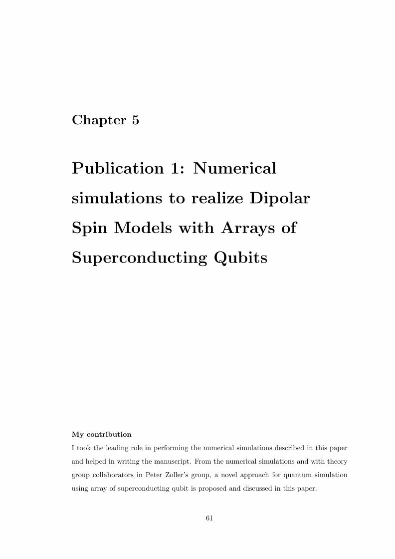
Chapter 5
Publication 1: Numerical
simulations to realize Dipolar
Spin Models with Arrays of
Superconducting Qubits
My contribution
I took the leading role in performing the numerical simulations described in this paper
and helped in writing the manuscript. From the numerical simulations and with theory
group collaborators in Peter Zoller’s group, a novel approach for quantum simulation
using array of superconducting qubit is proposed and discussed in this paper.
61

Qsim 62
This chapter covers the FEM based numerical simulations to realize spin models with
arrays of superconducting qubits.The basic building blocks are 3D Transmon qubits, uti-
lizing the naturally occurring dipolar interactions to realize interacting spin systems.
This opens the way toward the realization of a broad class of tunable spin models in
both two- and one-dimensional geometries. In collaboration with Peter Zoller’s theory
group we illustrate the potential offered by these systems in the context of dimerized
Majumdar-Ghosh-type phases, archetypical examples of quantum magnetism, showing
how such phases are robust against disorder and decoherence, and could be observed
within state-of-the-art experiments.
5.1 Motivation
In the present work we propose and analyze a novel setup for an analog quantum sim-
ulator of quantum magnetism using superconducting qubits. The scheme builds on the
remarkable recent developments in Circuit QED [85, 26, 86, 87, 88, 89] in the context of
quantum simulation [90, 91, 92, 93, 94], and especially the 3D Transmon qubit [30, 95].
The scheme (illustrated in Fig. 5.1) promises a faithful implementation of many-body
spin-1/2 Hamiltonians involving tens of qubits using state-of-the-art experimental tech-
niques. The central idea behind the present work is to exploit the naturally occurring
dipolar interactions between qubits to engineer the desired spin-spin interactions. In
combination with the flexibility offered by solid-state setups for realizing arbitrary ge-
ometry arrangements, this allows us to design general dipolar spin models in ladder
and 2D geometries. As we will show, our scheme competes favorably with present
and envisaged quantum simulation setups for magnetism with cold atoms and trapped
ions [96, 97, 98], and enables us to address some of the key challenges of quantum simu-
lation including equilibrium and non-equilibrium (quench) dynamics [99]. Moreover, we
note that exploiting dipolar interactions to design dipolar spin models is conceptually
different, and complementary to the remarkable recent experiments with superconduct-
ing circuits toward realizing the superfluid-Mott insulator transition, based on wiring
up increasingly complex circuits of superconducting stripline cavities [90]
In our analysis we address two of the key aspects of the design of our proposed simu-
lator for quantum magnetism. First, we present a feasibility study of state-of-the-art
experimental setups: this includes a discussion of the general mechanism to generate

Qsim 63
dipolar interactions between 3D Transmons, combined with ab initio simulations of the
coupling strength in our spin model for various geometries. Second, we illustrate how
state-of-the-art setups, composed of up to a dozen qubits and characterized by typical
disorder and decoherence rates, are already able to demonstrate paradigmatic signatures
of quantum magnetism. In particular, we show how a dimerized phase [100], a valence-
bond-solid reminiscent of the Majumdar-Ghosh state widely discussed in the context of
quantum spin chains [31], can be realized (via adiabatic state preparation) and probed
with current technologies.
The chapter is organized as follows. In Sec. 5.2, we introduce the XY model Hamiltonian,
and provide a short summary of the parameter regimes we are interested in. In Sec. 5.3,
we describe the circuit QED setup, and present detailed finite-element simulations to
access the relevant couplings in the systems, and describe their tunability. In Sec. 5.4, we
discuss a simplified circuit model, which provides a generic tool to understand the results
in Sec. 5.3. In Sec. ??, we perform a numerical study of the ground state properties of
the XY model on a triangular ladder, and discuss the observability of the dimer phase
using adiabatic state preparation. Finally, in Sec. 5.6, we draw our conclusions and
present a brief outlook.
5.2 Model Hamiltonian
The system dynamics we are interested in, is described by a generalized XY Hamiltonian
of the form
H/~ =∑i,j
J ′(θi, θj)
|rij |3(S+i S−j + h.c.) +
∑j
hjSzj (5.1)
where Sαj are spin operators at the lattice site j, rij is the distance vector between i
and j, and the inter-qubit couplings Jij =J ′(θi,θj)|rij |3 are in frequency units. The last term
describes a disordered transverse field, which reflects the disorder in the microscopic
qubit frequencies (i.e. Josephson energy).
The key element of our implementation is the realization of different patterns of quantum
frustration [100] by tuning the form of the interaction couplings (Fig. 5.4). As discussed
below, the latter display a rich dependence as a function of the dipole angles θj (see
Fig. 5.4b): this dependence is essential to tune the coupling between different spins
from positive to negative, or to (approximately) set it to 0. Even more crucially, the

Qsim 64
1/|rij |3 dependence (see Fig. 5.4a) can be exploited to further modify the magnitudes
of the couplings. In the theory of 1D and ladder systems [101, 102], where the dipo-
lar interaction is effectively local, this allows independent tunability of nearest-neighbor
(NN) and next-nearest-neighbor (NNN) exchange, a fundamental ingredient to realize
bond-order solids [31, 103]. We focus specifically on this case below, showing how, within
our proposal, such states of matter are robust against both disorder and qubit decoher-
ence. The setup can be straightforwardly extended to 2D geometries, where qualitatively
new features emerge due to the non-locality of the dipolar couplings: in particular, the
dynamics of Eq. (5.1) can by-pass the Mermin-Wagner-Hohenberg theorem [104, 105],
and thus support phases of matter with true long-range order even at finite tempera-
ture [106]. We emphasize that all of these phenomena are directly accessible within our
proposal thanks to the naturally occurring dipolar interactions, while such interactions
would be challenging to be implemented via wiring.
5.3 Circuit QED implementation of dipolar XY models
We now describe how the many-body dynamics of Eq. (5.1) can be realized in our setup,
using state-of-the-art circuit QED technology, with the design flexibility and long coher-
ence times 1/κ (κ ≤ 2π × 100 kHz) of Transmon qubits [30, 95]. This is schematically
illustrated in Fig. 5.1. Several Transmon qubits (in red) fabricated on a piece of sapphire
(light blue area) which are mounted inside a waveguide cavity (grey box). The Trans-
mon qubits can be fabricated in an essentially arbitrary lattice configuration with locally
controllable orientation. The waveguide cavity around the qubits is used to readout the
state of selected qubits and apply a drive to a subset of qubits, providing means for
both adiabatic state preparation and probing (see next section). This selectivity can be
again achieved by partially rotating the qubits inside the cavity by a few degrees, such
that their dipole moment has a finite overlap with the electric field in the cavity. To
add more flexibility to the setup, subsets of qubits can be fabricated on different pieces
of sapphire. For simplicity these individual pieces are not shown in Fig. 5.1. Using a
SQUID in the qubit circuit and a multi coil setup to change the flux for each qubit (as
realized in [107]), one should be able to reduce the disorder in the transition frequencies
to less than 1% (around 2π× 30 MHz spreading in hj) . This corresponds to a disorder

Qsim 65
strength in the model Hamiltonian of order δh ' 0.3, relative to the exchange matrix
elements Jij ' 2π ∗ 100MHz.
a
1 mm1 cm
J1
J2b c
Figure 5.1: Circuit QED implementation of spin models. (a) Drawing of one half of a waveg-uide cavity with two microwave coupler’s. Inside the cavity is a piece of sapphire with multipleTransmon qubits arranged on a triangular lattice. The rotation angles of the qubits are chosensuch, that only a few of them couple to the fundamental mode of the cavity with a predeterminedcoupling strength. (b) The cavity can be loaded with an arbitrary subset of qubits e.g. consider-ing the ones in the dot-dashed box in (a) realizes a triangular ladder. Here, the bond thicknessdenotes the interaction strength of nearest-neighbor (J1) and next-nearest-neighbor (J2) interac-tions. Additional longer-range contributions are represented by dashed lines (only the strongestare shown). (c) Sketch of the dimerized phase of the extended XY model in Eq. (5.1). The phasecan be understood as a solid of local triplet states, denoted by the shaded areas.
The unique feature of our approach is the design flexibility in the interqubit interaction
which results from the dipole-antenna structure of the Transmon. As one can expect, two
dipole antennas in the near field interact like two magnetic spins [108]. By designing
the shape and size of the antenna we can realize large interaction strengths (Jij ≈
2π × 100 MHz) at inter-qubit distances of about 1 mm. The interaction between the
qubits ultimately comes from an effective capacitance between the antennas, similar to
[91, 92], with an angle and distance dependence akin to magnetic dipoles.
5.3.1 HFSS simulations
To confirm and quantitatively assess the inter-qubit dipolar interactions, we have per-
formed a finite element study to determine the coupling strength and dependence on
distance and angle. These simulations are carried out by ab initio numerically solving
the 3D Maxwell equations on finite grids (HFSS software [109]), and as such provide an

Qsim 66
extremely accurate quantitative benchmark for our modeled inter-qubit couplings. The
quantitative insights gathered from the simulations are of basic importance to under-
pin the effects of the specific configuration that would be accessible in realistic setups,
where the influence of the surrounding waveguide cavity and finite size effects of the
Transmon antenna have to be systematically understood. It should be noted that finite-
element calculations of a structure with objects that are orders of magnitude different
in dimensions requires plenty of computational resources.
y
xz
Figure 5.2: Mesh used to calculate the electromagnetic fields around the qubits. The top lefthalf of the image shows the meshing needed for the cavity that contains a sapphire substrate withtwo qubits on it. The top right half shows meshing around one of the qubits. The coordinatesystem used in this paper is defined in the lower left.
In this work, extremely fine meshing is needed in areas where accurate understanding
of the physics of small objects (like qubits) is needed. Fig. 5.2 shows how different
mesh sizes are used for different structure size to accurately calculate the eigenmodes
of the electromagnetic fields of two qubits in a cavity. Typical cavity dimensions for
all simulations are: width= 2.5 cm, depth=3 cm, height=1 cm. In the following, the
coupling strength is defined as the minimum difference in the mode frequencies of two
qubits when the inductance of one qubit is swept in order to tune its mode frequency
in and out of resonances with the other(see Fig. 5.9). All simulations regarding the
coupling strength of the Transmon qubits were done with typical Transmon parameters

Qsim 67
i.e. EC ≈ 250 MHz,√
8EjEc ≈ 6 GHz and Ej/Ec ≥ 50. The antenna height used for
all simulations, unless otherwise specified, was 1 mm.
5.3.1.1 Single qubit inside cavity
J (M
Hz)
Distance from cavity wall (cm)
Cap
acit
ance
(fF
)
W (m)200 400 600 800
40
60
80
100
Linear fit
J (M
Hz)
a) b) c)Cosine fit
0.5 1.0 1.5 2.0
40
0
80
120
160
0.6 0.8 1.0 1.2 1.460
100
140
180
220
h (mm)
Linear fit
Figure 5.3: a) Extracted capacitance of the qubit as a function of the width of the antennapaddles. The dashed line is a linear fit to the data. b) Qubit-Cavity coupling strength g as afunction of its position inside the cavity. The qubit was placed in the center of the cavity inthe y and z direction and was moved along the x axis. The dashed line is a cosine fit to thedata. c) Coupling g of the qubit to the cavity as a function of its antenna length. Since a changein antenna length will also change the resonance frequency, the width of the antenna has beenadjusted to keep the resonance frequency constant. The dashed line is a linear fit to the data.
In order to better understand the effect of the antenna geometry on the qubit properties,
we start our analysis form the single qubit case. First, the width of the antenna pads
w was changed and the corresponding capacitance was extracted as shown in Fig. 5.3
a). It can be concluded that the capacitance increases linearly as a function of the pad
width.
Then, the coupling strength of the qubit to the cavity J was calculated as a function of
position of the qubit with respect to the side wall of the cavity. The coupling strength
has a cosine form as expected from a standing wave in the cavity. The results are shown
in Fig. 5.3 b).
The coupling strength J was also studied as a function of the pad height h as shown
in Fig. 5.3 c) where the qubit was located at the center of the cavity. It can be seen
from the figure that the coupling strength increases linearly as a function of the antenna
height. This is in agreement with dipole antenna physics.

Qsim 68
5.3.1.2 Coupling strengths from HFSS: Two-qubit case
A set of results can be seen in Fig. 5.4. Assuming a dipole-dipole interaction with an
additional component due to the dispersive coupling of both qubits to the cavity with
strength g (determined from independent simulations), we expect the following spatial
dependence:
J1,2 =g2d2
m
2∆sinφ1 sinφ2 +
− J0d2m
sin θ − 3 sin θ1 sin θ2
(r − rm)3. (5.2)
The first term takes into account the qubit-qubit interaction mediated via the funda-
mental cavity mode with φ1, φ2 the orientation of the qubits relative to the orientation
of the electric field in the cavity. Higher order cavity modes contribute with a similar
term with a coupling g′ depending on the mode structure; as these are typically very far
detuned, we neglect them in the following. The second term is the direct dipole-dipole
interaction between the qubits with r = |r12| being the distance between their centers.
Both, the qubit-cavity interaction strength (which depends on the location of the qubit
in the cavity) and the dipole-dipole interaction J0 get modified by the length of the
antenna, giving rise to the term dm in Eq. 5.2, with dm the normalized antenna length.
The remaining variables in this equation are the qubit cavity detuning ∆ ≈ 2π×1.5 GHz
and the angles θ1, θ2 with θ− = θ1− θ2. These are the angles formed by the two dipoles
with respect to a line connecting their centers, as can be seen in Fig. 5.4(b). rm corrects
for finite size effects of the dipole antennas.
One can see in Fig. 5.4(a) that the qubit-qubit interaction strength in our numerical
simulations very closely follows the analytical expression Eq. 5.2. The only fitting pa-
rameters in this expression are J0, which is the same for all three datasets, and the
rm, which is adjusted for each length. The dependence on the distance for different
antenna sizes can be seen in Fig. 5.4(a). The interaction strength between the qubits
for a parallel orientation is negative for short distances and falls of as 1/r3. For larger
distances it becomes positive due to the additional coupling mediated off-resonantly via
the cavity. This leads to the effect that qubits at a given distance (in the case of our
cavity about 3.5 mm) do not interact with each other as these terms exactly cancel out.

Qsim 69
1 2 3 4 5 7 961020
4060100200300
Rotation Angle θ (deg)
J /
(2 π
) (M
Hz)
- J
/ (2
π) +
20
(MH
z)
Distance r (mm)
θ
0306 090-60-300306090120150
a bi,j
i,j
θd
r
dm = 1dm = 1.4
dm = 0.6
m
Figure 5.4: Microscopic finite-element simulation (see text) of the dependence of the couplingJi,j between two qubits. Panel (a): distance dependence at θi = θj = 90 for three differentantenna length dm (given in mm). The dashed line indicates Ji,j = 0. The inset displays a typicalresult from HFSS simulations [109], with the dipoles surrounded by the computed electric field(intensity decreasing from red to blue). Panel (b): angular dependence illustrated for the caseθi = θj = θ at distance r = 1.5 mm. The solid line plots Eq. 5.2 with J0, rm extracted from bestfits in (a).
Such a canceling of the direct inter-qubit interaction can be very useful for quantum
information experiments.
By rotating one qubit around the other, as shown in Fig. 5.4(b), we can see that the
interaction strength goes from a negative value for a parallel orientation to a twice as
large positive value for collinear qubits, as expected for a dipole-dipole interaction. The
analytical curves agree well with the numerical simulations and demonstrate that the
spatial dependence of the interaction behaves like a magnetic dipole-dipole interaction.
Furthermore we note that the cavity mediated term can be fully suppressed by rotating
the qubits perpendicular to the electric field of the cavity mode, as shown schematically
in Fig. 5.1. The finite-element simulations are in very good agreement with a simple ana-
lytical circuit model described in the next section, which already captures the important
interaction features.
5.3.2 Additional simulations for two qubit
Further understanding more insight beyond paper.

Qsim 70
5.3.2.1 Moving one qubit along Y-axis
Two qubits are placed on a piece of sapphire separated by a distance of 1.5 mm. One
of the qubit is swept along the Z-axis, at a distance of 1 mm center to center distance
between qubits the interaction strength coupling ’J’ is zero. At a distance of 1 mm, the
angle between the qubits approaches to 35. From classical dipolar physics, when the
two dipole antennas are at an angle of 35 the coupling strength between the antennas
is zero [56].
10
1
0.11 2 3 4
d (mm)
'J' (
MH
z)
1.5 mm
'd' (
mm
)
X
Z
Y
Figure 5.5: The qubits are placed symmetric to the cavity and one of the qubit is swept alongthe y-axis. Coupling ’J’ as function of distance between the two qubits along Y-axis ’d’ for afixed distance along Z-axis.
5.3.2.2 Coupling strength as function of distance between two qubits back
to back on two sapphire chips
In this simulations, two qubits are placed in a cavity on two separate sapphire chips.
The distance dBB is varied to understand the qubit-qubit interaction with a vacuum
gap in between the sapphire chips. The interaction strength between the qubits goes
from a negative value to a positive value. As the distance of 1 mm between the qubits
the coupling strength is zero, the reason for this zero is that interaction strength goes
from a negative value to positive value and cavity mediated destructive and direct in-
terference. By further increasing the distance (dBB) the coupling strength between the
qubits becomes rapidly weaker. The maximum coupling strength ’J’ is obtained when
the two sapphire chips are touching each other. In this scenario, the coupling strength

Qsim 71
between the qubit’s is mainly influenced by the sapphire chips. Sapphire has a dielectric
constant of εr = 11, hence influencing the capacitive interaction between the qubit’s.
1
1 dBB (mm)
'J' (
MH
z)
X
Y
Z
2 3 4 5
350
300
250
200
150
100
50
0dBB (mm)
Figure 5.6: Coupling strength ’J’ as function of distance between two qubits mounted back toback dBB . In the illustration transmon qubits are placed on two sapphire chips of about 330 µmthickness. The coupling strength J reduces quickly to 10’s of MHz because of the increaseddistance between the sapphire substrates.
5.3.3 Changing the coupling in-situ
To add more flexibility to the setup, each row of qubits can be fabricated on an individual
piece of sapphire. These two pieces can then be moved relative to each other (e.g. along
the z-direction) via a piezo actuated stage (as e.g. used in [110, 111]) which allows for
an in-situ change of the coupling ratio J2/J1. As the distance for all qubits in one row
does not change J2 stays constant. In contrast J1 will vary with the distance of the two
sapphire pieces. How the ratio of J2/J1 changes when the sapphire pieces are moved
apart along the , can be seen in Fig. 5.7.
One can see that changing the distance by about 100 µm changes the coupling ratio by
about a factor of two. Typical piezo actuators allow a positioning to much better than
1 µm over distances of a few millimetres, making this approach technically challenging
but feasible. In order to be able to move the sapphire pieces, the sapphire has to pass
through the cavity wall via thin slit. This thin slit will be a waveguide below cut off and
poses no problem for the desired (rather low) quality factor of the cavity. Once outside
the superconducting wall, the sapphire can be clamped to the piezo stage.
The two sapphire pieces can also be moved along the y-direction, which is perpendicular
to the illustration in Fig. 5.7. This would again change the coupling between the rows

Qsim 72
as illustrated in Fig.2 in the main text. For feasible parameters a change of about a
millimeter, would be necessary to change the coupling ratios from about 0.25 to 1.
0 50 100 150 200 250
40
60
80
100
120
140
160
180J
(MH
z)
Distance S (µm)
J2J1J2/J1
0.2
0.4
0.6
0.8
1.0
1.2
J 2/J
1
Sz
y
Figure 5.7: Coupling J1 and J2 and the ratio J2/J1 as a function of distance S between qubitrows. This simulation was run with a 1 mm antenna. Each row of qubits in the ladder model canbe fabricated on an individual piece of sapphire. These two pieces can then be moved relativeto each other via a piezo actuated stage which allows for an in-situ change of the coupling ratioJ2/J1. As the distance for all qubits in one row does not change J2 stays constant. In contrastJ1 will vary with the distance of the two sapphire pieces. The inset shows a side view of the twosapphire pieces with the two rows of qubits (red blocks) on top. The two rows are offset fromeach other on the two sapphires. This offset can be adjusted to match the desired couplings forS approaching zero.
5.3.4 Qubit state measurement and Flux tuning
An advantage of a circuit QED setup is the ability to measure the state of a predeter-
mined but otherwise arbitrary subset of qubits in the lattice. A measurement of 〈Szi 〉 can
be realised in circuit QED by probing the cavity transmission in the limit of a dispersive
qubit cavity coupling. With the newly developed quantum limited amplifier technology
it is nowadays possible to detect quantum jumps of an individual qubit [33, 112] and
the parity of a two qubit state [87]. Using this measurement techniques one has to take
into account the strong interaction between the qubits, which means that a direct mea-
surement of 〈Szi 〉 in the uncoupled basis is not possible [113]. We would rather project

Qsim 73
onto one of the eigenstates of the coupled system which might be useful for an initial
evaluation of the interaction but would not tell us anything about the actual properties
of the state.
This effect can be avoided by effectively switching off the coupling by detuning a subset
of qubits from each other and all other qubits by more than J in a time faster than 1/J
in order to be non adiabatic. This detuning can be achieved by realizing the qubits one
wants to measure with a SQUID instead of a single Josepshon junction. The challenge in
the 3D architecture is, to realize a fast tune-ability of the flux through the SQUID. Some
of the problems that typically appear are a slow response time of the flux bias circuit
and a possibility of an oscillation of the flux due to ringing of the circuit. These led to
the development of fast flux bias lines and several methods to eliminate the response of
the line by deconvolution methods solved by using a magnetic hose [114, 115].
In our case the requirements on the flux bias lines are reduced. We do not care about a
small uncertainty in the qubit frequency after the flux change as additional dephasing
won’t be relevant for the measurement of 〈Szi 〉. If ringing of the circuit proves to be a
problem, one could use an asymmetric SQUID design for the Transmon qubit [116] and
use both flux sweet spots to reduce flux sensitivity. Furthermore, we do not care about
addressability as only a subset of qubits will be sensitive to the flux. Also we only need
two flux configurations: (1) all qubits in resonance and (2) the qubits that have to be
measured sufficiently detuned from the rest.
Combining these relaxed requirements should allow us to adjust the flux with the help
of small coils (50-100 nH) just outside the cavity made out of copper hose [115]. Sim-
ulations and preliminary room temperature experiments show that a current of ≈ mA
is sufficiently large to generate the desired flux. Changing the current in one of these
coils will effect more than one qubit, though with different magnitude. Adjusting the
currents in different closely spaced coils using e.g. an optimal control algorithm should
in principle allow us to generate the desired flux values for our application at the qubit
location even though there are inter-dependencies. The switching times will be limited
by Eddy currents in the cavity wall. These can be reduced by implementing the flux
bias lines inside the cavity with appropriate filtering to avoid an undesired coupling of
the cavity or qubit to the environment.

Qsim 74
Another method to measure correlations functions of interacting qubits coupled to a
cavity was recently published in a very similar context [117]. In this paper the authors
show that the spectrum of the resonator is directly related to the correlation function of
the coupling operator between the resonator and the interacting qubits. This method can
be adapted in the context of our proposal and be used to readout correlation functions.
Even more information can be extracted by making use of multiple resonator modes
with different coupling to the qubits. The advantage here is, that no fast switching of
the magnetic bias field is necessary.
5.4 Circuit model
In this section, details of a circuit model that represents two-qubits inside a cavity are
explained. The model is used to evaluate the coupling strength between the elements,
and support the HFSS simulations.
5.4.1 Circuit diagram
Dissipation-less LC resonators are used to model the cavity and qubits (see also [118]
or [119] for a refined method including dissipation). The nonlinearity of the qubits is
not taken into account as it does not affect the coupling strength. Capacitors are used
in order to account for the coupling between elements. The coupling between each qubit
and the cavity is represented by a coupling capacitor Cqcav. As qubits are assumed to
couple to each other through their dipole antenna, a total of four capacitors are used to
represent coupling of each antenna pad to the two pads of the other qubit (see Fig. 5.8).
5.4.2 Coupling strength
In order to calculate the coupling between elements, the following method is used: The
impedance of the system (Zin) seen through one of the qubits (here Q1) is calculated.
The poles of the impedance are the resonance modes of the total system, in this example
three. By sweeping the inductance L1 (of Q1) we can see the avoided crossing between
the modes (see Fig. 5.9). Coupling is defined as the minimum distance between the two
modes at the avoided crossing.

Qsim 75
Ccav Lcav
Q2 Q1
CqcavCqcav
Zin
10-4 10-2 100
s (m)
10-7
10-5
10-3
10-1
101
c ab
Wa WbS
aL aR bL bR
a) b)
Q2 Q1
Figure 5.8: a) Circuit model corresponding to two qubits in a cavity. Values of the fourcapacitors drawn in red decay as 1/r2 where r is the center to center distance between pads ofthe antenna. This models the dipole-dipole coupling of two qubits. The two purple structures onQ1 and Q2 represent the physical shapes of the qubits. b) Capacitance between two co-planarpaddles (solid line) as a function of the separation s according to equation 5.3. The correspondingstructure is shown at the bottom. The dashed line shows the quadratic decay used in this studyto estimate the coupling capacitance. The structure at top right shows which capacitors in thecircuit model follow the quadratic decay.
A further step was taken by relating the inter-qubit coupling capacitances (as in Fig. 5.8
a)) to the physical distances among the qubit antenna poles. This distance dependence
is assumed to be of the following form [120]:
Cab = (2ε/π) ln(aL − bL)(aR − bR)
(aR − bL)(aL − bR)
= (2ε/π) ln(w + s)2
(w + s)2 − w2
(5.3)
where ε is the average over dielectric constants of the substrate and the air (or vacuum),
w = wa = wb is the width of antenna paddles and s is the separation between closest
edges as shown in the inset of Fig. 5.8 b). The parameters aL, aR, bR, bL are defined in
Fig. 5.8 b).
As this study concerns square shaped paddles (see top right inset of Fig. 5.8b)), it is
not possible to apply equation 5.3 to any arbitrary relative position of the two qubits
without complicated corrections. Therefore, just to demonstrate the general behavior,
a simplified relation (Eq. 5.4 follows Eq. 5.3 when the separation s becomes much larger
than the paddle width w - this effect is shown in Fig. 5.8 b)) for the coupling is chosen
which assumes that the capacitance decays quadratically as a function of the distance:
Cab =a
s2(5.4)

Qsim 76
where a is a coefficient used to adjust the coupling strength.
This means that the coupling strength Ji,j can be calculated based on the physical
position of the two qubits with respect to each other. In this study, Q1 is assumed to
be fixed in position and Q2 changes its distance and angle with respect to Q1.
Q1 uncoupled
Q1 coupled
Q2
Cavity
3 4 5 6 7 8 9 10 11 125.0
5.5
6.0
6.5
7.0
7.5
8.0
8.5
9.0
9.5
L1 (nH)
Mod
e fr
eque
ncy
(GH
z)
2J
2g
Figure 5.9: Example for three modes of a system with two qubits and a cavity.The minimumdistance of two modes is defined as the coupling 2Ji,j if it is two qubits and as 2g if it is the qubitcavity coupling. Note that despite the fact that Q2 has 9 nH of inductance, the crossing happensat lower inductances due to the coupling to Q1. Dashed line shows how resonance frequency ofa typical LC circuit would behave without coupling to the other resonators.
Assuming that the two qubits are placed parallel with respect to each other, we have
calculated the coupling Ji,j as a function of the center-to-center distance. In Fig. 5.10
the results are shown for two qubits without a mediating cavity. As can be seen, the
coupling is heavily suppressed along a straight line. This line can be thought of as when
the dipole electric field from Q1 is horizontal, that is perpendicular to the dipole antenna
of Q2 and hence, there will be no coupling. This is typical behavior of dipoles and is well
expected. However, by adding a cavity to the model (see Fig. 5.10 b)), one can observe
that the straight line shape of suppression will no more hold and instead, a curved line
emerges.
Adding the cavity has certain consequences on how two qubits couple. For example, if
one moves Q2 along the x-axis while it is held at y = 1 mm (or y = −1 mm), the coupling
might be suppressed twice. This is verified by HFSS simulations as seen in Fig. 5.4. Our

Qsim 77
-40
0
90
-Jij / (2) (MH
z)
a) b)
1 2 3 4X (mm)
1
2
3
4
Y (
mm
)
1
2
3
4
Y (
mm
)
1 2 3 4X (mm)
Figure 5.10: a) Contour plot showing the coupling strength between two qubits Ji,j as afunction of the distance between them, in the x and y direction, in absence of the cavity. Thecolor scale is logarithmic to highlight the rapid change in Ji,j . In such a case, the dipole physicsdominates and the coupling will be suppressed along a straight line. The white area is notaccessible due to the dimensions of the qubits. b) Contour plot showing the coupling strengthbetween two qubits Ji,j as a function of the distance between them, in the x and y direction, inpresence of the cavity. The color scale is logarithmic to highlight the rapid change in Ji,j . Thecavity distorts the straight line of suppressed coupling opening new possibilities for engineeringof the coupling between two qubits. The white area is not accessible due to the dimensions ofthe qubits.
lumped-element model shows behavior that matches the HFSS simulations, as can be
seen in Fig. 5.11.
5.5 Hamiltonian derivation
In this section, I briefly review the derivation of the microscopic spin Hamiltonian be-
tween interacting Transmons.
5.5.1 Interacting Transmons
Let’s consider two interacting transmons as depicted in Fig. 5.12. The Lagrangian
describing this system is given by
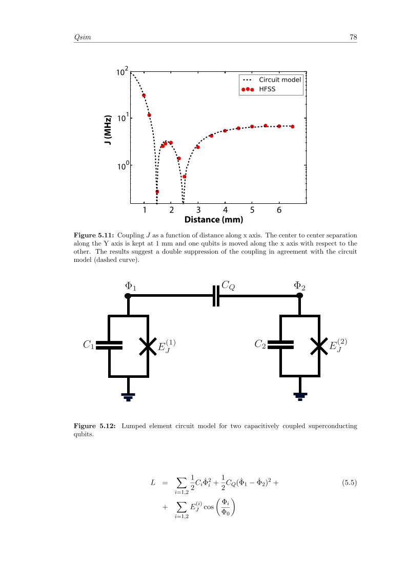
Qsim 78
Distance (mm)1 2 3 4 5 6
J (M
Hz)
102
101
100
Figure 5.11: Coupling J as a function of distance along x axis. The center to center separationalong the Y axis is kept at 1 mm and one qubits is moved along the x axis with respect to theother. The results suggest a double suppression of the coupling in agreement with the circuitmodel (dashed curve).
Figure 5.12: Lumped element circuit model for two capacitively coupled superconductingqubits.
L =∑i=1,2
1
2CiΦ
2i +
1
2CQ(Φ1 − Φ2)2 + (5.5)
+∑i=1,2
E(i)J cos
(Φi
Φ0
)

Qsim 79
with Φ0 ≡ ~/(2e). The Hamiltonian, H =∑
i=1,2QiΦi − L can then be written as
H =1
2~QTC−1 ~Q−
∑i=1,2
E(i)J cos
(Φi
Φ0
), (5.6)
with ~ΦT ≡ (Φ1,Φ2). For small phase fluctuations, I can expand the cosine and get
H = H0 +H1, with
H0 =1
2~QTC−1 ~Q+
1
2~ΦTL−1~Φ (5.7)
H1 ≈ −∑i=1,2
E(i)J
24Φ40
Φ4i , (5.8)
where
C =
C1 + CQ −CQ
−CQ C2 + CQ
,
C−1 =1
D
C2 + CQ CQ
CQ C1 + CQ
,
L−1 =
1/α1 0
0 1/α2
,
D ≡ C1C2 + C1CQ + C2CQ and 1/αi ≡ E(i)J /Φ2
0. Now by quantizing this Hamiltonian
using the usual ladder operator replacement for Qj and Φj which is
Qj = iQZPFj (a†j − aj),Φj = ΦZPF
j (a†j + aj), (5.9)
where QZPFj ≡
√~ωjCeff
j /2, ΦZPFj ≡
√~ωjαj/2, Ceff
1 ≡ DC2+CQ
, Ceff2 ≡ D
C1+CQ. Here,
ω1, ω2 are the two solutions of |L−1 − ω2C| = 0. This quantization gives
H ≈∑i=1,2
ωini −∑i=1,2
Λin2i + λ12(a†1a2 + h.c.), (5.10)
where Λj ≡E
(j)J4
(ΦZPF
j
Φ0
)4
, λ12 ≡CQ
D QZPF1 QZPF2 , and nj ≡ a†jaj . Notice that this
Hamiltonian has been written in a basis of local modes. Diagonalization of the quadratic

Qsim 80
part via a Bogoliubov transformation gives rise to a Hamiltonian of the form [118]
H ≈∑i=1,2
ξini −∑i=1,2
αin2i − χ12n1n2. (5.11)
5.5.2 Interacting transmons inside a cavity
R
Figure 5.13: Lumped element circuit for two interacting superconducting qubits in a cavityresonator.
Let’s now consider the circuit depicted in Fig. 5.13 which is a simplified version of the
circuit shown in Fig. 5.8 a) with the capacitive coupling network between the qubits
reduced to one capacitor. This transformation can be easily done for a fixed qubit-qubit
distance. The simple lumped element model will provide the right Hamiltonian but does
not capture the angle and distance dependence explicitly. The Lagrangian of the system
is given as
L =∑i=1,2
1
2CiΦ
2i +
∑i=1,2
E(i)J cos
(Φi
Φ0
)(5.12)
+1
2CΦ2
R −Φ2R
2L+
1
2CQ(Φ1 − Φ2)2
+∑i=1,2
1
2C0(Φi − ΦR)2.

Qsim 81
The associated Hamiltonian H = H0 +H1 can be written as equations (5.7) and (5.8),
with
C =
C1 + CQ + C0 −CQ −C0
−CQ C2 + CQ + C0 −C0
−C0 −C0 C + C0
,
L−1 =
1/L1 0 0
0 1/L2 0
0 0 1/L
.
Here, Li ≡Φ2
0
E(i)J
. Quantizing this Hamiltonian gives
H ≈∑
i=1,2,R
ωini −∑i=1,2
Λin2i + (5.13)
+∑
i 6=j=1,2,R
λij(a†iaj + h.c.),
with similar expressions for the coupling constants as in Eq. (5.10) 1. Here, the qubit
and cavity are far detuned. However, the qubit-cavity coupling may be sufficiently
large to mediate virtual transitions between both qubits through the cavity. This effect
will be relevant whenλiRλjR
∆j∼ λ12, where ∆j ≡ −ωj + ωR. Performing a canonical
transformation
H → eSHe−S , (5.14)
with
S ≡∑i=1,2
εiR(a†iaR − a†Rai), (5.15)
and taking εiR ≈ −λiR∆i
, and obtain to second order in the transformation, an effective
Hamiltonian (in a rotating frame with respect to the resonator)
Heff ≈∑i=1,2
∆ini −∑i=1,2
Λin2i + (5.16)
+∑
i 6=j=1,2
Jij(a†iaj + h.c.),
1For the qubit-cavity coupling the capacitance CQ is substituted by C0 in such expressions.

Qsim 82
with the renormalized constants are related to the original energies as
∆i = −∆i(1− ε2iR), (5.17)
Λi = Λi(1 + 4ε2iR), (5.18)
Jij = λij +λiRλjR
2∆j, (5.19)
where i = 1, 2. The Hamiltonian (5.16) can be readily generalized for N qubits by letting
i = 1, . . . , N , and conveniently diagonalized into the form written in Eq. (5.11). Also, it
can be written in a spin language, by considering sufficiently large qubit anharmonicities.
Typical anharmonicities for Transmon qubits in the range of 200 − 300 MHz are suffi-
cient to realize a successful state preparation, while still staying in the Transmon limit
(EJ/EC > 40). This allows us to replace the Bosonic operators by spin 1/2 operators, so
the effective Hamiltonian for two capacitively coupled superconducting Transmon qubits
inside a cavity is given by
Heff ≈∑i
ωiSzi +
∑i 6=j
Jij(S+i S−j + h.c.). (5.20)
Note that the angle and distance dependence of the qubit coupling is hidden in the Jij
in this derivation.
5.6 Conclusions
From the finite element numerical simulations, we show how to use the naturally oc-
curring dipolar interactions in 3D superconducting circuits to realize a platform for
analogue quantum simulation of XY spin models. The possibility of realizing arbitrary
lattice geometries with locally-tunable dipole moments [29], in combination with their
large interaction strength, opens the door to the investigation of a series of phenom-
ena in quantum magnetism in both 1D [121, 122] and 2D [106], complementing the
remarkable developments in cold atom and trapped ion systems [96, 97, 98]. The idea
discussed in this chapter [29] are not limited to Transmon qubits, but could be imple-
mented with, e.g., Xmon qubits [89] or Fluxonium qubits coupled to an antenna [123].
It would be interesting to explore these developments in view of realizing Hamiltonian

Qsim 83
dynamics for surface code architectures [8] or as a building block for coupled cavity array
experiments [124, 125].

Chapter 6
Publication 2: Characterization
of low loss microstrip resonators
as a building block for circuit
QED in a 3D waveguide
My contribution
I have contributed in designing the High-Q microstrip resonators and writing the manuscript.
The numerical simulations for designing the MSR’s and characterization of the devices is
initially carried out by me. In collaboration with other authors, the final characterization
results are discussed in this paper.
84

Microwave stripline resonators 85
Here we present the microwave characterization of microstrip resonators made from
aluminum and niobium inside a 3D microwave waveguide. In the low temperature, low
power limit internal quality factors of up to one million were reached. We found a
good agreement to models predicting conductive losses and losses to two level systems for
increasing temperature. The setup presented here is appealing for testing materials and
structures, as it is free of wire bonds and offers a well controlled microwave environment.
In combination with transmon qubits, these resonators serve as a building block for a
novel circuit QED architecture inside a rectangular waveguide.
6.1 Motivation
Microwave resonators are an important building block for circuit QED systems where
they are e.g. used for qubit readout [126, 127], to mediate coupling [128] and for para-
metric amplifiers [34]. All of these applications require low intrinsic losses at low temper-
atures (kBT hfr) and at single photon drive strength. In this low energy regime, the
intrinsic quality factor, which quantifies internal losses, is often limited by dissipation
due to two level systems (TLS) [129, 130]. These defects exist mainly in metal-air, metal-
substrate and substrate-air interfaces as well as in bulk dielectrics [130, 131, 132, 133].
Two common approaches exist, to improve the intrinsic quality factor of resonators.
Either one reduces the sensitivity to these loss mechanisms by reducing the participa-
tion ratio [130, 59, 134] or tries to improve the interfaces by a sophisticated fabrication
process [135, 136]. Reducing the participation ratio requires to reduce the electric field
strength. This is typically done by increasing the size of the resonator [132] or even
implementing the resonator using three dimensional structures [59].
6.2 Design of a MSR in a waveguide
Our approach, a microstrip resonator (MSR) in a rectangular waveguide (Fig. 6.1),
combines the advantages of three dimensional structures with a compact, planar de-
sign [127, 30]. The sensitivity to interfaces is reduced, since the majority of the field
is spread out over the waveguide, effectively reducing the participation ratio [134]. An-
other advantage is, that the waveguide represents a clean and well controlled microwave

Microwave stripline resonators 86
environment [56] without lossy-seams [137] close to the MSR. As the MSR is capacitively
coupled to the waveguide, no wirebonds [138] or airbridges [139] are required, which can
lead to dissipation or crosstalk.
The U-shaped MSR (Fig. 6.1 a)) is a capacitively shunted λ/2 resonator. Due to the
open end, a voltage maximum occurs at the ends and a current maximum in the cen-
ter [56]. Considering that the MSR is patterned on silicon, the resonance frequency
of the fundamental mode is expected at 11.3 GHz. The additional shunt capacitance
between the legs shifts the resonance frequency down to about 8 GHz.
x
y
23 in mm
11
0.1
3.653.1
1
a)b)
H
Figure 6.1: MSR layout. a) Sketch of the MSR on a substrate. b) Sketch of the cross sectionof the waveguide with MSR inside. The dashed line indicates the electric field strength of thefundamental mode inside the waveguide.
The coupling of MSR, depends on the position of the MSR in the waveguide along the
x-axis. A critically coupled setup is inevitable to get trustworthy results of Qint and Qc,
in particular in the single photon limit. To accomplish such a setup, simulations were
performed.
6.2.1 Finite element simulations on the coupling
To estimate the coupling between the MSR and the waveguide, numerical simulations
using finite element solver was performed.
Figure 6.2 illustrates the two considered cases. At first, the MSR was swept from the
center towards the wall. Fig. 6.3 a) shows the results of the coupling. A critically
coupled setup in the single photon limit requires a coupling quality factor on the order
of 1× 10⁵ to 1× 10⁶, depending on the measured MSR. In the available waveguides,
there are only discrete slots to place the sample. The first off-centered slot is around

Microwave stripline resonators 87
xx12.6 m
m
21 mm 10.5 mm
a) b)
Figure 6.2: Sketch of the simulated setups. a) In simulations the MSR was shifted from thecenter towards the wall. b) MSR placed in the center with an additional sapphire substrate nextto it, which displaces the field inside the waveguide. This leads to an asymmetry of the electricfield over the centrally placed MSR, thus a non vanishing coupling. In simulations the substratewas shifted from the MSR towards the wall.
0 2 4 6 8 2 3 5 6104
105
106
102
105
103
4
104
QC
QC
Off-center =x (mm) Distance to sapphire = x (mm)
a) b)
Figure 6.3: Simulation results of the coupling quality factor for different positions of the MSRin the waveguide. a) MSR shifted from the center to the waveguide wall (illustrated in Fig. 6.2a)). b) MSR placed in the center and the empty substrate being shifted away towards the wall(Fig. 6.2 b)).
3 mm from the center, which leads to a coupling quality factor between 1× 10³ and
1× 10⁴, being around two magnitudes below critically coupled.
To displace the electric field in the waveguide, the MSR is placed in the center and an
empty sapphire substrate in a neighbouring slot, due to the higher εr of sapphire. This
is illustrated in Fig. 6.2 b). From the simulations with the MSR placed in the center
and the empty substrate being shifted towards the wall (Fig. 6.3 b)). The substrate
being one slot off center (neighbouring the MSR) leads to a coupling of around 1× 10⁵.
For two slots off center the desired coupling quality factor reaches around 1× 10⁶. It is
important to note, that for such high coupling quality factors, effects like the MSR having
a slightly asymmetric leg length, or being placed off center on the chip or placed entirely
off center, can have a big impact on the coupling. For instance simulations showed, that
a displacement of 0.2 mm off-center, can lead to a factor of 4 in the coupling quality

Microwave stripline resonators 88
factor.
6.3 MSR and aluminium waveguide in detail
In this section, the photographs of the MSR on the silicon substrate, the MSR in the
waveguide and the completely assembled waveguide are shown.
a) b) c)
Figure 6.4: a) Photograph of a MSR with uneven leg length. b) Photograph of MSR placedinside the rectangular waveguide. Illustration, including dimensions of the waveguide and theMSR in Fig. 6.2. c) Mounting process. The MSR is slid in from the top. Two metal rods areused as guidance.
Figure 6.4 shows a photograph of the MSR a) and the MSR in the waveguide b). In c)
the process of mounting the MSR is shown. The MSR is assembled to a holder and slid
from the top into the waveguide.
Figure 6.5: Photograph of totally assembled waveguide. The waveguide used for the transmis-sion measurement consist of three parts. In the middle section, three rows of samples can bemounted. In this picture only the middle row is used for a sample.
Fig. 6.5 shows the fully assembled waveguide. The waveguide consists of three parts.
At each end there is an identical coupler to receive and launch the microwave signals.

Microwave stripline resonators 89
The central part contains the samples. In this design no seams are present near the
samples. It is possible to probe three samples, each in one of the three slots, which can
be easily extended to more samples by using a different central section. One can see
the individual slots for each sample, customized to the dimensions of our sample. In
contrast to this waveguide, the copper waveguide only allows to probe a single sample
at a time.
For microwave transmission measurements, the MSR is placed in a rectangular waveg-
uide (Fig. 6.1 b)). The fundamental TE10 mode, which has electric field components
only along the z-axis, is the sole propagating mode at the resonance frequency of the
MSR. Its field strength varies along the x-axis with a maximum in the center [56] (dashed
line in Fig. 6.1 b)). For the MSR placed off-center, the field strength is different on both
legs, which leads to a capacitive coupling to the waveguide. Placed in the exact center
of the waveguide, the field strength is equal on both legs of the MSR and the coupling
vanishes. The coupling of the MSR in the waveguide, can also be varied with legs of
different length. To accurately predict the interaction of the MSR with the waveguide
numerical simulations is performed using a finite element solver.
MSRs are characterized in waveguides fabricated from oxygen free copper or aluminum.
The waveguides were mounted to the baseplate of a dilution refrigerator and cooled down
to 20 mK. The MSRs were analyzed regarding their resonance frequencies and quality
factors by measuring S21. The measured data is fitted using a circle fit routine [140]
which utilizes the complex nature of the S-parameter.
6.4 Measurement results
To assess the performance of different materials, aluminum and niobium MSRs is inves-
tigated. The samples were fabricated using standard optical lithography techniques and
sputter deposition of the metallic films. Structuring of the metal layer was done using a
wet etching process for the aluminum samples and a reactive ion etching (RIE) process
for niobium. After completely removing the photoresist, both samples were cleaned in
an oxygen plasma.
Two sets of measurements were performed. First, the MSRs are measured under vari-
ation of input powers, ranging from below the single photon limit to several million

Microwave stripline resonators 90
photons circulating in the resonator. Second, to understand the TLS effects, the base
temperature is ramped up to 1 K and performed measurements at single photon powers.
6.4.1 Internal quality factor dependence on circulating photon number
and temperature
Fig. 6.6 a) shows the dependence of the internal quality factor on the circulating photon
number in the MSR. All measurements show a clear trend of an increasing quality factor
with the number of photons. This indicates that the MSRs are limited by TLS losses,
as they get saturated with increasing drive powers [129]. From the measurements the
highest single photon internal quality factor of one million for the two niobium MSRs
placed in the aluminum waveguide. For high powers a Qint of more than 8 million is
measured. Other experiments, using a more sophisticated fabrication process, report
similar internal quality factors for planar NbTiN resonators on deep etched silicon [135]
or for planar aluminum resonators on sapphire [136]. Similar methods and materials
might allow us to increase the single photon quality factor of the MSR.
0.0 0.4 0.80.0
0.4
0.8
1.2
1
0.1
0.01
0.4
0.0
0.4
0.8
Qin
t X 1
06
0.5
1.0
1.5
2.0
100 104 108
n
Qin
t X 1
06
T (K)
a) b)
0.0 0.4 0.8
Figure 6.6: Dependence of the internal quality factor on a) the circulation photonnumber in the MSR and b) the temperature (Al MSR). Nb MSR in Cu waveguide.
Nb MSR in Al waveguide. Al MSR in Al waveguide. Al MSR in Cu waveguide.a) All but one MSR/waveguide combinations show a clear increase of the internal quality factorwith increasing photon number. The only exception is the MSR in the copper waveguide whichseems to be limited by other losses. Both Nb MSRs in the aluminum waveguide show an internalquality factor of one million at the single photon limit. The measurements were taken at 20 mK.b) Internal quality factor of Al MSR in dependence of temperature, measured with single photonpowers. The data are fitted to a model (dashed lines) combining decreasing TLS related losses(Eq. 6.2) and losses due to an increasing surface resistance with temperature (Eq. 6.1)
.
The trend of increasing Qint is weakest for the aluminum MSR in the copper waveguide,
which indicates that this MSR is not limited by TLS. Due to the normal conducting cop-
per waveguide does not shield external fields. Thus vortices might limit the performance
Microwave stripline resonators 91
of the aluminum MSR in the copper waveguide [141]. This effect is not observed for the
niobium MSR, due to its higher critical field [142]. The difference in quality factor of
the niobium stripline in the copper and in the aluminum waveguide can be attributed to
losses to the copper wall, as suggested by simulations. When increasing the temperature
of the MSRs, two effects on the internal quality factors are expected. Approaching the
critical temperature leads to a decrease of Qint, due to an increasing surface impedance.
Considering a two fluid model [143], the following temperature dependence is found
1
QRsint
=A
Texp
(− ∆
kBT
)+
1
Qother. (6.1)
Here T is the temperature, ∆ the superconducting gap at zero temperature, kB the
Boltzmann constant and A a constant. An additional Qother accounts for other tem-
perature independent losses. This model is expected to show good agreement until
Tc/2. [144]
TLS saturate with increasing temperature, which leads to an increase in quality fac-
tor [129]1
QTLSint
= k tanh
(hfr(T )
2kBT
)+
1
Q′other
. (6.2)
Where k is the loss parameter and hfr(T ) represents the energy of the TLS at the
resonance frequency of the MSR for a given temperature. The resonance frequency
barely changes with temperature (Fig. 6.7 b)), which allows us to fix the frequency of
the TLS to the resonance frequency of the MSR in the low temperature limit. Q′other is
analogue to Eq. 6.1.
Figure . 6.6 b) shows the dependence of the internal quality factor of the aluminum MSRs
on the base temperature of the dilution cryostat. The data is fitted to a combined model
of TLS related losses (Eq. 6.2) and conductive losses (Eq. 6.1). Until about 200 mK the
MSRs in the copper waveguide show a constant internal quality factor. This gives
further evidence that dissipation due to TLS is not the dominant loss mechanism for the
aluminum MSRs in the copper waveguide. In the aluminum waveguide an increase in
Qint with temperature until 200 mK is observed. Thus in this waveguide, TLS related
losses most likely limit the quality factor of the MSR. Above 400 mK all MSRs show
a similar decrease in Qint. This can be attributed to conductive losses, as the critical
temperature of aluminum is around 1.19 K [144]. Near the critical temperature, an

Microwave stripline resonators 92
internal quality factor slightly above 1000 is measured. This is close to the results of
finite element simulations, which predict an internal quality factor of about 500.
Δf r(k
Hz)
Qin
t (x1
06 )
T (K)
fr (
kHz)
0.0 0.4 0.8-1
0
1
2
1.0
1.5
2.0
0.0 0.4 0.8T (K)
a) b)
Figure 6.7: Temperature dependence of the Nb MSRs. Nb MSR in Cu waveguide.Nb MSR in Al waveguide. a) Internal quality factor of the niobium MSR at single photon
powers. The data is fitted (lines) to the TLS model, Eq. 6.2. For the MSR in the aluminumwaveguide, this model breaks down around 350 mK, when losses of the waveguide walls becomedominating. Therefore data points above 350 mK are disregarded for the fits. b) Resonancefrequency shift of the MSR at ≈ 106 photons. The data is fitted to the model described byEq. 6.3. In the copper waveguide good agreement is observed until around 800 mK (data pointat 1 K is omitted for the fit). In the aluminum waveguide, above 350 mK the observed frequencychange is dominated by the waveguide walls (as in a)).
6.4.2 Internal quality factors and frequency of Nb MSR with respect
to temperature
Figure 6.7 a) shows the temperature dependence of the internal quality factor of the
niobium MSRs. Niobium has a critical temperature of about 9.2 K [144], hence a break-
down of superconductivity isn’t observed. Thus, the data is only fitted with the model
describing TLS related losses (Eq. 6.2). The behavior of the MSR in the copper waveg-
uide agrees well with predictions from theory throughout the whole measurement range.
An increase of Qint up to 1 K is observed. For the MSR in the aluminum waveguide a
drop in the internal quality factor at 350 mK is measured. In this region the breakdown
of superconductivity for the aluminum MSRs (Fig. 6.6 b)) is observed. This indicates
that the breakdown of superconductivity in the waveguide walls is the limiting factor
here. For higher temperatures, the internal quality factor remains approximately con-
stant around 1× 10⁶. Performing finite element simulations using the finite conductivity
of the aluminum (Al5083 [145]) waveguide wall a Qint of 1.16× 10⁶ is observed, which
is consistent with our measurements.

Microwave stripline resonators 93
TLS also lead to a shift in the resonance frequency [129]
∆fr(T ) = fr(0)k
π×(
ReΨ
(1
2+
1
2πi
hfr(T )
kBT
)− log
(1
2π
hfr(T )
kBT
)). (6.3)
Here Ψ is the complex digamma function. Fig. 6.7 b) shows the frequency shift when
increasing the temperature of the cryostat. In contrast to the effect on Qint, off reso-
nant TLS contribute to the frequency shift [129], which makes the resonance frequency
independent of power. The only fit parameter is the combined loss parameter, k. For
measurements of the Nb MSR in the aluminum waveguide, a drop in the frequency shift
above 350 mK is observed. This again is due to the breakdown of superconductivity in
the waveguide wall. Below 350 mK, the measurements are in good agreement with the
model.
The values obtained for k by fitting the shift of the resonance frequency are about 10%
to 30% lower, than fitting the change of the internal quality factor (Fig. 6.7 a)). This
can be attributed to a non-uniform frequency distribution of TLS [129], which leads to
a difference whether Qint or ∆fr is considered. The intrinsic quality factor depends on
losses to TLS near the resonance frequency, whereas the shift of the resonance frequency
depends on a wider frequency spectrum of TLS.
An approximate low power, low temperature limit on Qint is given by 1/k. Taking the
k value found fitting the change of Qint gives a 20% to 30% higher limit, than found
in the measurements. This suggests that the majority of losses happen to TLS, but
there is also a second loss mechanism. According to simulations, the internal quality
factor of the MSR in the copper waveguide could be limited by the wall conductivity.
In the aluminum waveguide it could be attributed to bulk dielectric loss from the high-
resistivity silicon, as the loss tangent is not very well known [139].
The MSR in the waveguide represents a resonator in notch configuration [140]. For such a
resonator, the S21 parameter, which refers to a transmission measurement, follows [140]:
S21(f) = 1− Ql/|Qc|eiφ0
1 + 2iQlf−frfr
(6.4)
Here Ql is the total quality factor, fr is the resonance frequency and Qc is the coupling
quality factor. In here φ0 accounts for an impedance mismatch in the transmission line

Microwave stripline resonators 94
before and after the resonator, which makes Qc a complex number (Qc = |Qc|e−iφ0).
The real part of the coupling quality factor determines the decay rate of the resonator,
in our case the emission to the waveguide. The physical quantity is the decay rate, κ,
which is inversely proportional to the quality factor [146] and therefore the real part is
found as: 1/QRec = Re(1/Qc) = cosφ0/Qc. Knowing QRec and Ql, the internal quality
factor can be obtained, as 1/Ql = 1/QRec + 1/Qint [146]. Plotting the imaginary versus
the real part of S21 forms a circle in the complex plane (in case of a resonance within
the frequency range).
Equation 6.4 represents an isolated resonator, not taking effects from the environment
into account. Including the environment, which arises by including the whole measure-
ment setup before and after the MSR, hence the equation is modified as . 6.4 to [140]:
S21(f) = (aeiαe−2πifτ )
(1− Ql/|Qc|eiφ0
1 + 2iQlf−frfr
)(6.5)
Here a and α are an additional attenuation and phase shift, independent of frequency. τ
represents the phase delay of the microwave signal over the measurement setup, which
has a linear dependence on frequency.
6.4.3 Tuning coupling of MSR to the waveguide
Fig. 6.8 illustrates the actually measured configurations. In the copper waveguide a) - e),
one sample was measured each time, in the aluminum waveguide, three samples could be
measured at once, labelled (f1)-(f3) in the following. The three samples in the aluminum
waveguide were put along the propagation direction, all in the same configuration. As
they MSRs had to have different resonance frequencies, one MSR had longer legs (f3),
leading to a nominally lower resonance frequency of around 0.5 GHz. This MSR, as well
as a second one (f2), having a resonance frequency of nominally 8 GHz, is backed with
an empty silicon substrate. This reduces the resonance frequency, due to the higher
effective dielectric constant.
The measurement results are plotted in Fig. 6.9, are in good agreement with the sim-
ulation data. The weak dependence on the number of photons agrees well with the
expected power-independence of the coupling. The closer the MSR is to the wall, the
lower the coupling quality factor a), b), inline with simulations. With the additional

Microwave stripline resonators 95
21
2.75 12.6
5.85
5.858.95 8.953.1
4.2
23
9.953.1
9.95
23
11
a) b)
c) d)
e) f)
Figure 6.8: Measured configurations of MSRs in the waveguide. The orange border refers toa waveguide made from copper, the gray border to one made from aluminum. In the copperwaveguide, one sample was tested at each time, whereas in the aluminum waveguide threesamples were tested at once, refereed to as (f1)-(f3). The dimensions of the different waveguidesare stated. All dimension in mm.
empty substrate, the quality factors follow the predictions from simulations c), d). For
the substrate further away from the MSR, d)- f), highest coupling quality factors are
observed. The difference in the coupling between configurations d), e) and (f1), which
should be similar (the only nominal difference is the waveguide width) to a slight dis-
placement of the MSR as discussed before. The quality factors of (f2) and (f3) are
higher, as they are already backed with an empty substrate. Thus the relative influence
of the neighbouring substrate is reduced, leading to a higher Qc.
6.4.4 Resonance frequency in dependence of photon number in the
MSR
The measured resonance frequencies are shown in Fig. 6.10. The additional silicon sub-
strate backing reduces the resonance frequencies of the 7.5 GHz(f3) and 8 GHz(f2) MSRs,

Microwave stripline resonators 96
0.001 0.1 10 1e+03 1e+05 1e+07 1e+09photons in resonator
1e+03
1e+04
1e+05
1e+06Qc
a
a
b
b
c
c
d
d
e
e
f1
f1
f2
f2
f3
f3
Figure 6.9: Coupling quality factor for different configurations (see Fig. 6.8). The lines depictthe simulated data, the points are the measurements.
aa
bb
cc
dd
ee
f1f1
ab
cd
ef1
f2f3
0.01 10 1e4 1e77.2
7.4
7.6
7.8
8.0
7.9
7.92
7.94
7.96
0.01 10 1e4 1e7
f r (
GH
z)
f r (
GH
z)
n n
a) b)
Figure 6.10: Resonance frequencies for the different configurations (see Fig. 6.8) in dependenceof photon number. The lines depict the simulated data, the points are the measurements. a) Allmeasured configurations. b) Configurations with nominally the same resonance frequency. Thedeviation of the simulated resonance frequency for configuration c) can be explained with thecloser sapphire substrate, compared to the other setups. The sapphire leads to a higher effectiveεr and thus a lower resonance frequency.
plotted in (i). Except (f1), simulation results accurately predict the resonance frequen-
cies. All the other setups have resonance frequencies in the same range (Fig. 6.10(ii)),
which is predicted by simulations. There are several explanations for the 70 MHz devia-
tion of the resonance frequency, which is not seen in the simulation data. One possibility
is, a variance in the chip dimension. This would lead to a different effective dielectric
constant and thus a lower resonance frequency. Other possibilities include a slight dif-
ference between the MSRs or its placement on the substrate.
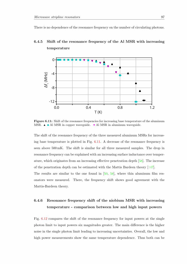
Microwave stripline resonators 97
There is no dependence of the resonance frequency on the number of circulating photons.
6.4.5 Shift of the resonance frequency of the Al MSR with increasing
temperature
T (K)
0.0 0.4 0.8 1.2
Δf r (
MH
z)
0
-4
-8
-12
Figure 6.11: Shift of the resonance frequencies for increasing base temperature of the aluminumMSR. Al MSR in copper waveguide. Al MSR in aluminum waveguide.
The shift of the resonance frequency of the three measured aluminum MSRs for increas-
ing base temperature is plotted in Fig. 6.11. A decrease of the resonance frequency is
seen above 500 mK. The shift is similar for all three measured samples. The drop in
resonance frequency can be explained with an increasing surface inductance over temper-
ature, which originates from an increasing effective penetration depth [58]. The increase
of the penetration depth can be estimated with the Mattis Bardeen theory [147].
The results are similar to the one found in [59, 58], where thin aluminum film res-
onators were measured. There, the frequency shift shows good agreement with the
Mattis-Bardeen theory.
6.4.6 Resonance frequency shift of the niobium MSR with increasing
temperature - comparison between low and high input powers
Fig. 6.12 compares the shift of the resonance frequency for input powers at the single
photon limit to input powers six magnitudes greater. The main difference is the higher
noise in the single photon limit leading to increasing uncertainties. Overall, the low and
high power measurements show the same temperature dependence. Thus both can be
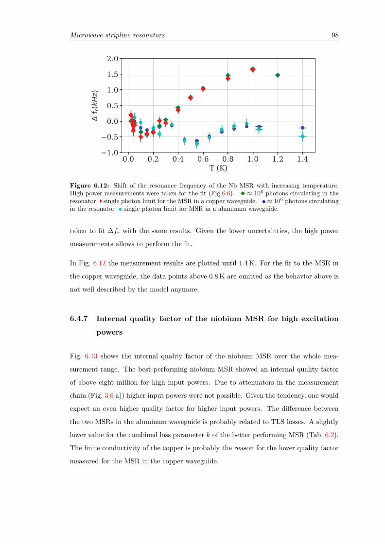
Microwave stripline resonators 98
Figure 6.12: Shift of the resonance frequency of the Nb MSR with increasing temperature.High power measurements were taken for the fit (Fig.6.6). ≈ 106 photons circulating in theresonator single photon limit for the MSR in a copper waveguide. ≈ 106 photons circulatingin the resonator single photon limit for MSR in a aluminum waveguide.
taken to fit ∆fr with the same results. Given the lower uncertainties, the high power
measurements allows to perform the fit.
In Fig. 6.12 the measurement results are plotted until 1.4 K. For the fit to the MSR in
the copper waveguide, the data points above 0.8 K are omitted as the behavior above is
not well described by the model anymore.
6.4.7 Internal quality factor of the niobium MSR for high excitation
powers
Fig. 6.13 shows the internal quality factor of the niobium MSR over the whole mea-
surement range. The best performing niobium MSR showed an internal quality factor
of above eight million for high input powers. Due to attenuators in the measurement
chain (Fig. 3.6 a)) higher input powers were not possible. Given the tendency, one would
expect an even higher quality factor for higher input powers. The difference between
the two MSRs in the aluminum waveguide is probably related to TLS losses. A slightly
lower value for the combined loss parameter k of the better performing MSR (Tab. 6.2).
The finite conductivity of the copper is probably the reason for the lower quality factor
measured for the MSR in the copper waveguide.

Microwave stripline resonators 99
Figure 6.13: Similar to Fig. 6.6 a) but showing the full measurement range of the niobiumMSR. The internal quality factor reaches nearly ten million. Nb MSR in copper waveguide.
Nb MSR in aluminum waveguide.
6.4.8 Fit results
The internal quality factor of the MSR changes with temperature. In case of the niobium
MSR this is explained with the loss to two level systems (Eq.6.2). By fitting this model
to the measurement data (Fig.6.7 a)). TLS also lead to a shift of the resonance frequency,
predicted by Eq. 6.3. The measurement results including the fits are shown in Fig. 6.7
b).
In case of the aluminum MSR, an increasing surface resistance also leads to an additional
effect on Qint, next to the TLS. Thus a combined model of the surface impedance
(Eq. 6.1) and TLS (Eq. 6.2) for the fit is used:
1
QTLS + Rsint
= k tanh
(hfr(T )
2kBT
)+A
Texp
(− ∆
kBT
)+Qother (6.6)
To fit this model to the change of Qint, the inverse of Eq. 6.6 was taken. The fit
parameters of all performed fits are listed here. In Tab. 6.1 the fit results of Eq. 6.6 to
the measurements of the aluminum MSR (Fig. 6.6 b)) are given.
In case of the aluminum MSR in the copper waveguide, 1/k can not be taken as a low
energy low temperature limit for Qint, as the MSR is limited by other losses. Only the
MSR in the aluminum waveguide, being limited by TLS related losses, 1/k = 6(1)× 105,
is in agreement with the measurements. In turn, it was not possible to extract a useful

Microwave stripline resonators 100
Table 6.1: Fit results including fit errors for the measurement of the internal quality factorof the aluminum MSR, for stepwise increasing temperature. The results including the fits areshown in Fig. 6.6 b). The corresponding model is given in Eq. 6.6. Given that the the MSRs inthe copper waveguide are not limited by TLS related losses, the fit values are not trustworthy.A similar conclusion can be drawn for the MSR in the aluminum waveguide, for Qother. TheMSR seems to be either limited by TLS or surface impedance losses, so Qother is not seen in themeasurement.
A Qother k
Al - cu ( ) 5.6(7)× 10−4 4(1)× 105 1.2(6)× 10−6
Al - cu ( ) 10.2(9)× 10−4 0.92(2)× 105 4.46× 10⁻¹ ± 2.1
Al - al ( ) 6.5(7)× 10−4 - 1.6(2)× 10−6
value for Qother, as the MSR was either limited by TLS effects or increasing conductive
losses. For the MSRs in the copper waveguide Qother is in agreement with the measure-
ments. The values obtained for A, which refers to the increasing surface impedance, are
in the same range for all measurements.
Tab. 6.2 lists the fit results for the niobium MSR. The change of the internal quality
factor with temperature (Fig. 6.7 a)) and the change of the resonance frequency with
temperature (Fig. 6.7 b)) is fitted. For the niobium MSR the k can be either determined
Table 6.2: Fit results including fit errors for the measurement of the internal quality factor ofthe niobium MSR, for stepwise increasing temperature. The measurement results including thefits are shown in Fig. 4. The corresponding model for the change of Qint is given in Eq.6.2 andfor the change of the resonance frequency in Eq. 3.
fit to Qint(T ) fit to ∆fr(T )k Qother k
Nb - cu ( ) 10.0(2)× 10−7 2.53(4)× 106 9.1(5)× 10−7
Nb - al ( ) 7.5(4)× 10−7 4.7(5)× 106 5.6(3)× 10−7
Nb - al ( ) 7.9(7)× 10−7 7(2)× 106 6.1(4)× 10−7
by fitting the change of Qint or the change of the resonance frequency. In both cases
the value obtained are in the same range. Nevertheless, the value obtained fitting the
resonance frequency is throughout 10% − 30% higher, than fitting Qint. The reason
lies in the frequency distribution of the TLS [129]. In addition, the Qint limit given
through k. Qother gives an upper limit on the internal quality factor. The fit values are
compatible with the measurements (Fig. 6.13).
Microwave stripline resonators 101
6.5 Conclusion
The characterized MSRs show single photon intrinsic quality factor of up to one million
at 20 mK. A strong dependence of the internal quality factors on the photon number
and the temperature indicates losses to two level systems. The design presented is
appealing for testing material of the MSR, the substrate it is patterned on and for
validating fabrication processes. However, the observed quality factors are expected to
increase when more complex designs are used, such as suspended structures [133] or by
improving the surface quality through deep reactive ion etching [135].

Chapter 7
Publication 3: Bi-Stability in a
Mesoscopic Josephson Junction
Array Resonator
My contribution
I have taken the lead role in designing, characterization and the measurements described
in this paper, and the writing of the manuscript. In collaboration with other authors,
the measured data is analysed theoretically.
102

Josephson Junction Array resonator 103
We present an experimental investigation of stochastic switching of a bistable Josephson
junctions array resonator with a resonance frequency in the GHz range. As the device
is in the regime where the anharmonicity is on the order of the linewidth, the bistability
appears for a pump strength of only a few photons. We measure the dynamics of the
bistability by continuously observing the jumps between the two metastable states, which
occur with a rate ranging from a few Hz down to a few mHz. The switching rate strongly
depends on the pump strength, readout strength and the temperature, following Kramer’s
law. The interplay between nonlinearity and coupling, in this little explored regime, could
provide a new resource for nondemolition measurements, single photon switches or even
elements for autonomous quantum error correction.
7.1 Motivation
The non-linearity provided by atoms and Josephson junctions is a necessary ingredient
to observe quantum mechanical effects in cavity quantum-electro-dynamics (QED) and
circuit QED (cQED) systems. Strong nonlinearites, much larger than the linewidth
of the transition, are required to realize qubits [30], implement quantum information
protocols [148, 149] and realize textbook quantum optics experiments [150, 151]. Non-
linearities much smaller than the linewidth of the transition are typically exploited for
parametric processes [45, 152, 36] like amplification or frequency conversion at the quan-
tum level.
Besides quantum information applications, there has been a growing interest to exploit
cavity QED for ultralow-power classical logic elements [153, 154, 155]. This interest
has been sparked by the ever growing all optical communication networks. Remark-
ably, a single photon transistor [156], reminiscent of an electronic transistor, has been
implemented for the optical domain. In this device a single photon can switch a large
optical field. Realizing such devices has been a challenging endeavour as the required
non-linearity is hard to realize, due to the weak interaction of optical light with atoms.
Much stronger light matter interactions can be achieved in the microwave regime using
the cQED platform. In this context Josephson junction arrays (JJAs) have proven to
be an ideal circuit element to build superconducting qubits with excellent coherence
properties and unique tuning capabilities [157, 158, 159]. Similarly, JJAs have also been

Josephson Junction Array resonator 104
used to build quantum limited parametric amplifiers [160, 161, 36, 162]. Recently, the
coherence properties of the self resonances of JJAs [163, 43], as well as their self-Kerr and
cross-Kerr coefficients have been measured [51]. The measured Kerr coefficient showed
good agreement with a model based on a second order expansion of the Josephson
potential [164].
A regime of particular interest arises when the self-Kerr Ki and cross-Kerr Kij nonlinear
coefficients are on the order of the linewidth κ of the system. In this regime the system
will show a pronounced bistability [165, 54] at the single to few photon level. Bistability is
a phenomenon which is relevant in many fields, ranging from chemistry [166] and biology
[167, 168] to Josephson junction physics [169, 170] and cQED [171]. Very recently, an
optically levitated nanoparticle has been shown to exhibit a stochastic bistability [172]
and Kramers turnover [173].
This chapter reports on the realization of a JJA resonator with multiple modes and
strong self-Kerr and cross-Kerr coefficients in the regime Ki,Kij ≈ κ. Further by in-
vestigating the bistability of one mode of the JJA and characterize the dependence of
the switching rate on the pump strength, readout strength and temperature. In addi-
tion, the numerical model, based on Kramer’s’ theory (described in the last section of
chapter 2), is in good agreement with the experimental observations.
7.2 Device Description
The JJA consists of 103 cascaded Josephson junctions, with a small capacitance to
ground C0, coupled to a 6 mm long microwave antenna and a shunt capacitance Cs, as
shown in Fig. 7.1. The junctions are fabricated on a sapphire substrate using electron
beam lithography and bridge-free double-angle evaporation [174]. An electron beam
image of the junctions can be found in Fig. 7.1d. The junctions were designed to
have a large ratio EJ/EC ≈ 200, in order to suppress coherent quantum phase slips
(CQPS) [175, 43]. Here EJ is the Josephson junction energy and EC is the charging
energy. The parameters of the JJA were designed such that the fundamental resonance
of the JJA combined with the shunt capacitance is around 1 GHz. The mode spacing
for the first 10 modes is about 1.2 GHz and progressively becomes smaller for higher
resonances [43, 51].

Josephson Junction Array resonator 105
a) b)
Antenna
c) d)
600 nm
Cg
50 W 50 W
IN OUT
C0
LJ, CS
CJ
Wav
egui
de1mm
Figure 7.1: a) Photograph of one half of a rectangular copper waveguide with a 6 GHz cutoff. AJJA with a microwave antenna is fabricated on a piece of sapphire and placed in the center of thewaveguide b) Schematic representation of an array of Josephson junctions inside a waveguide.C0 is the capacitance of the islands to ground, CS is the shunt capacitance for the array, CJ is thejunction capacitance and Cg denotes the coupling capacitance of the antenna to the waveguide.LJ is the Josephson junction inductance. The input and output couplers to the waveguide areshown on the top left and top right of the schematic. (c) Optical image of the JJA coupled to a6 mm long antenna and a shunt capacitance. The inset shows a zoom-in on the junction array.(d) Electron beam image (blue box in the inset) of ten of the 103 Josephson junctions.
The JJA is placed inside a copper waveguide [176] with a 6 GHz cutoff, as shown
in Fig. 7.1a. Due to the capacitive coupling of the JJA to the waveguide, we can
characterize the sample by performing microwave transmission measurements using a
vector network analyzer (VNA). Due to the relative symmetry of the electric field of
the waveguide and the antenna, the even modes of the JJA will couple poorly to the
waveguide and not be visible in transmission measurements. The waveguide with the
sample is mounted on the mixing chamber stage (10 mK) of a cryogen free dilution

Josephson Junction Array resonator 106
4.81 4.82
|S21
| (dB
)
Frequency (GHz)
0
-20
|S21| (
dB)
Frequency (GHz)7.1 7.12
a)c)-40
-60
-50
-70
9.275 9.28
-35
-40
-45
|S21| (
dB)
Frequency (GHz)
d)
0 20 4030101.0
1.2
1.4
1.6
Time (s)
Am
plitu
de (
mV
)
b)
c)
Figure 7.2: Transmission measurements, measured with a power corresponding to about onephoton circulating in the resonator. The solid line in a), (c), (d) is a fit using Eq. 7.1 to extractQtot and ωR. a) Resonator response measurement for mode five b) Relaxation time T1 on modefive with a pump strength of nP = 115 photons. The solid line is an exponential fit to the datawith T1 = 3 µs. (c) Resonator response measurement for mode seven. (d) Resonator responsemeasurement for mode nine.
refrigerator. The sample is enclosed in a double layer cryoperm shield inside a completely
closed copper can. The stainless steel input lines are attenuated with 20 dB at 4 K and
30 dB at base temperature. They are filtered with a combination of a 12 GHz low pass
and an Eccosorb filter. The output stage consists of a 12 GHz low pass filter, two 4-
12 GHz isolators and a 4-8 GHz high electron mobility transistor amplifier. The effective
measurement bandwidth for direct transmission measurements using a VNA is limited
to about 4-9 GHz due to the cutoff of the waveguide and the combined bandwidth of
other microwave components.

Josephson Junction Array resonator 107
Within the accessible measurement bandwidth three resonances are characterized by
fitting their transmission data to a notch type response function [177] given by eq.7.1.
From these measurements the resonance frequencies (ωi/2π), the internal and the cou-
pling quality factors is extracted shown Fig.7.2 and Table. 7.1.
S21 = 1−1
Qi,ext− 2i δf
ωi/(2π)
1Qi,tot
+ 2iω−ωiωi
. (7.1)
The parameter δf takes into account an impedance mismatch. The extracted parameters
are summarized in Table 7.1.
Mode ωi/2π Qtot κi Ki Ki7
(GHz) (kHz) (kHz) (kHz)
5 4.816(1) 26000 181 66 187
7 7.1058(2) 950 7500 133 -
9 9.278(1) 3375 2750 218 343
Table 7.1: Parameters for the three array modes that can be directly measured with the VNA.fr and Qtot were extracted from data. The Kerr and cross-Kerr coefficients are calculated froma fit to the dispersion relation Fig. 7.3d.
Fig. 7.2b shows a measurement of the decay time T1 of mode five for a pump strength
of about nP = 115 photons. To excite the resonator the pump was detuned by about
-2.54 MHz from the bare frequency ωP /2π = 4.8156 GHz of mode five. Similar to a
two-tone measurement we use mode seven as a readout, with a readout strength of
nR = 0.5 photons. To perform the decay time measurement we excite mode five for a
few µs with a pulse before performing a readout on the pump mode again using a pulse
of a few µs. By varying the delay between the two pulses we measure how the excitation
decays over time. From the measurements we find T1 ≈ 3µs.
To observe the resonances of the modes outside the measurement bandwidth, we ex-
ploit the cross-Kerr interaction, which is induced by the junction non-linearity. The
Hamiltonian for the JJA, up to second order, is given by
H/~ =
N∑i=1
(ωia†iai +
Ki
2a†iaia
†iai) +
N∑i,j=1i 6=j
Ki,ja†iaia
†jaj . (7.2)
The Hamiltonian consists of a self-Kerr term Ki which leads to a photon number ni =
a†iai dependent frequency shift of mode i and a cross-Kerr interaction Kij , which leads
to a frequency shift of mode i depending on the photon number in all other modes j.

Josephson Junction Array resonator 108
7.3 Two-tone spectroscopy
Since the other resonance frequencies of the JJA’s are out of the HEMT amplification
bandwidth or below the cutoff frequency of the waveguide, we utilize a two-tone mea-
surement technique to indirectly measure them. We use mode seven as read-out and
apply a second pump tone. We sweep the frequency of this pump tone from 960 MHz
to 20 GHz. Such a two-tone spectroscopy measurement can be seen as a pump probe
experiment. The VNA is used to monitor one mode while a signal generator is used to
excite a second one. We then observe the shift in the read-out mode due to populating
other resonances through the pump tone. From this we can observe e.g. the fundamental
mode of the array at 963 MHz and other higher resonant modes up to 20 GHz which
is the limit of our signal generator. Two tone measurements for our array are shown in
Fig 7.3.
Figure 7.3d, shows the dispersion relation of the array. The frequencies outside the
HEMT bandwidth are extracted by two-tone spectroscopy measurements as shown in
Fig.7.3a, b, c. The mode spacing for the first 10 modes is about 1.2 GHz. For higher
resonant modes the spacing between modes becomes smaller. The • in Fig 7.3d are
obtained by diagonalizing the capacitance matrix which includes the shunt capacitance
(Cs), junction capacitance (CJ), the ground capacitance (C0) and the Josephson induc-
tance (LJ) for the entire array structure. From the fit the obtained JJA parameters
are C0 = 0.152 fF, CJ = 34 fF, LJ = 1.25 nH, CS = 18 fF with a confidence range
of about 20 %. These parameters match well to the expected design values and room
temperature resistance measurements of the junctions. With these parameters, the self-
kerr Ki and the cross-kerr Ki,j can be calculated using a procedure similar to Ref. [51].
The results are summarized in Table 7.1 of for modes five, seven and nine. Using these
coefficients the photon number is calibrated by measuring the resonance frequency shift
as a function of the applied power as shown in Fig.7.5. The attenuation extracted
from these Kerr measurements matches within 4% to the attenuation in the cryostat,
determined by independent transmission measurements. Most of the even modes can
not be observed from two tone measurements as the electric field distribution of these
modes has a symmetry that does not couple to the waveguide. For higher mode numbers
this symmetry is somewhat broken due to inhomogeneities of the junctions and we can
again excite these modes. It should also be noted that a discrepancy between the model
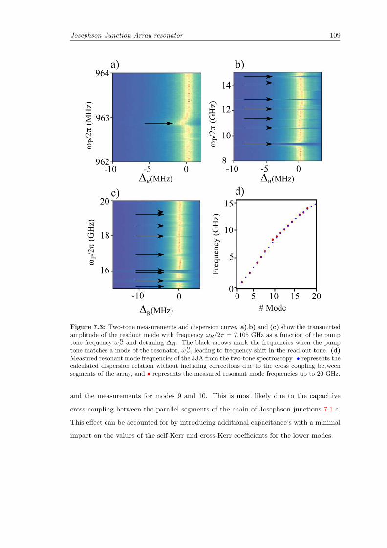
Josephson Junction Array resonator 109
0 5 10 15 20
10
5
0
15F
requ
ency
(G
Hz)
# Mode
962
963
964
-10 -5 0R(MHz)
P/2
(MH
z)
8
10
12
14
-10 -5 0R(MHz)
-10 0
20
18
16
R(MHz)
a) b)
c) d)
P/2
(GH
z)
P/2
(GH
z)
Figure 7.3: Two-tone measurements and dispersion curve. a),b) and (c) show the transmittedamplitude of the readout mode with frequency ωR/2π = 7.105 GHz as a function of the pumptone frequency ωD
P and detuning ∆R. The black arrows mark the frequencies when the pumptone matches a mode of the resonator, ωD
P , leading to frequency shift in the read out tone. (d)Measured resonant mode frequencies of the JJA from the two-tone spectroscopy. • represents thecalculated dispersion relation without including corrections due to the cross coupling betweensegments of the array, and • represents the measured resonant mode frequencies up to 20 GHz.
and the measurements for modes 9 and 10. This is most likely due to the capacitive
cross coupling between the parallel segments of the chain of Josephson junctions 7.1 c.
This effect can be accounted for by introducing additional capacitance’s with a minimal
impact on the values of the self-Kerr and cross-Kerr coefficients for the lower modes.
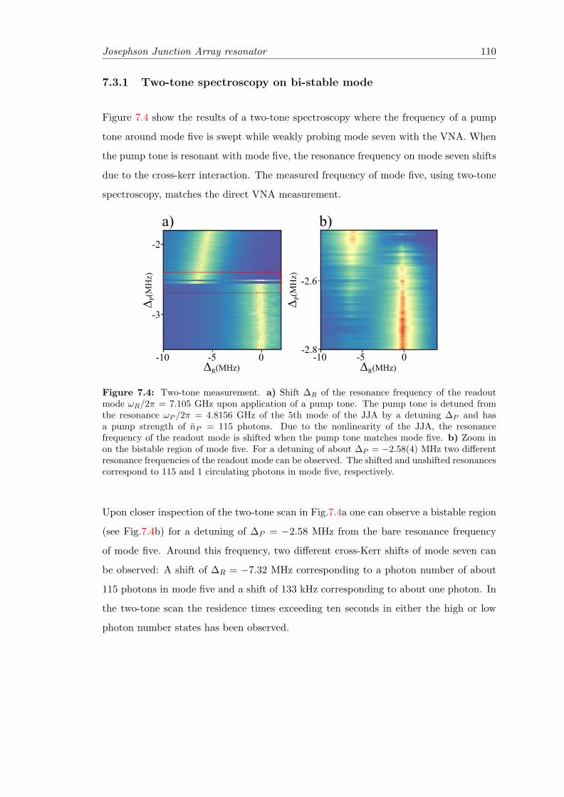
Josephson Junction Array resonator 110
7.3.1 Two-tone spectroscopy on bi-stable mode
Figure 7.4 show the results of a two-tone spectroscopy where the frequency of a pump
tone around mode five is swept while weakly probing mode seven with the VNA. When
the pump tone is resonant with mode five, the resonance frequency on mode seven shifts
due to the cross-kerr interaction. The measured frequency of mode five, using two-tone
spectroscopy, matches the direct VNA measurement.
P(M
Hz)
R(MHz) R(MHz)-10 -5 0 -10 -5 0
-3
-2
-2.6
-2.8
P(M
Hz)
a) b)
Figure 7.4: Two-tone measurement. a) Shift ∆R of the resonance frequency of the readoutmode ωR/2π = 7.105 GHz upon application of a pump tone. The pump tone is detuned fromthe resonance ωP /2π = 4.8156 GHz of the 5th mode of the JJA by a detuning ∆P and hasa pump strength of nP = 115 photons. Due to the nonlinearity of the JJA, the resonancefrequency of the readout mode is shifted when the pump tone matches mode five. b) Zoom inon the bistable region of mode five. For a detuning of about ∆P = −2.58(4) MHz two differentresonance frequencies of the readout mode can be observed. The shifted and unshifted resonancescorrespond to 115 and 1 circulating photons in mode five, respectively.
Upon closer inspection of the two-tone scan in Fig.7.4a one can observe a bistable region
(see Fig.7.4b) for a detuning of ∆P = −2.58 MHz from the bare resonance frequency
of mode five. Around this frequency, two different cross-Kerr shifts of mode seven can
be observed: A shift of ∆R = −7.32 MHz corresponding to a photon number of about
115 photons in mode five and a shift of 133 kHz corresponding to about one photon. In
the two-tone scan the residence times exceeding ten seconds in either the high or low
photon number states has been observed.

Josephson Junction Array resonator 111
7.4 Kerr coefficients and photon number calibration
7.4.1 Self-Kerr measurements
For the self-Kerr measurements only one mode i of the chain is excited. The frequency
shift ∆P with respect to the input power is measured using direct transmission mea-
surements. Each data-set is fitted with a notch type response function to extract the
frequency ωi and Qi,tot. From the shift relative to the bare resonance frequency the
self-Kerr coefficient Ki is extracted.
5 (
MH
z)
0.0
-1.0
-2.0
0.0
0
0.0
-2.0
1 2 0 5
0 1 2 0
Power (nW)Power (nW)
Power (nW) Power (nW)
a) b)c) (d)
c) d)
5 10
0.0
-1.0
-1.0
2.5 7.5
-2.0
-4.0
-6.0
(
MH
z)
(
MH
z)
5 (
MH
z)
Figure 7.5: Self-Kerr and cross-Kerr measurements. The error on each data point is aboutpoint size. a) Dependence of the self-Kerr frequency shift on the input power of mode five. Thered line is a third order polynomial fit - see text. b) Dependence of the self-Kerr frequency shifton the input power of mode seven. The red line is a linear fit - see text. (c) Cross-Kerr frequencyshift of mode seven when applying input power to mode five. The red line is calculated usingthe theoretical prediction for the linear self-Kerr term - see text. The read-out mode seven isdriven with about nR ≈ 0.5 photons. (d) Cross-Kerr frequency shift of mode five when applyinginput power to mode seven. The red line is a polynomial fit to the data. The read-out mode fiveis driven with about nR ≈ 1 photons.
Fig. 7.5a shows the self-Kerr measurements on mode five. For low input power P the
resonance frequency ∆5 changes linearly with power. For high input power, higher order

Josephson Junction Array resonator 112
Kerr terms (K ′i,K′′i ) start to play a role. To take this into account the data is fit with the
following dependence. With this the Kerr coefficients are extracted in units of Hz/W.
∆i(P ) = KiP +K ′i2P 2 +
K ′′i3P 3 (7.3)
Fig. 7.5b shows the self-Kerr measurements on mode seven. Here the resonance frequency
∆7 changes linearly with the power due to the higher linewidth (κ7) of this mode.
7.4.2 Cross-Kerr measurements K75 utilizing two-tone spectroscopy
The cross-Kerr coefficients Kij are determined by utilizing two-tone spectroscopy mea-
surements. One mode i of the array is used as the readout with a power of about one
photon and the other mode j is excited with varying power. From the shift ∆R of the
resonance frequency of the readout mode ωR/2π upon application of a pump tone, the
cross-Kerr shift Kij is extracted. Figure 7.6 a) shows a typical two-tone spectroscopy
measurements to extract the cross-Kerr coefficient K75 by pumping mode five and ob-
serving the frequency shift on mode seven. Mode seven is driven with a constant readout
strength of nR = 0.5 photons. To extract the maximal frequency shift ∆R, each pump
frequency of the data is fit to a notch type response function and extract the resonance
frequency(solid black line). The maximal shift of the readout resonator for a given
pump power results in one datapoint in Fig. 7.5 c). Figure 7.6 b)-c) shows the two-tone
spectroscopy for different pump powers. From the measurement in Fig. 7.6 one can also
clearly observe that the mode becomes bistable as the power is increased. Figure 7.5 c)
shows the result of all two tone measurement to determine the cross-Kerr shift K75
when driving mode five and using mode seven as the readout. For low input power the
resonant frequency ∆7 changes linearly with the power but then rapidly higher order
terms come into play. In this case, even a third order polynomial fit does not agree with
the measured K75. Thus the cross-Kerr coefficient has been characterized by fitting the
slope at low powers in Fig. 7.5c. By using the dispersion relation fit in Fig. 7.3d and the
resulting diagonalized capacitance matrix, the ratio between K5 and K75 is extracted.
This ratio, together with K5 determined from the linear part of the fit function Fig. 7.5a
allows us to compute K75. A linear fit with the computed slope K75, shown by the
solid red line in Fig.7.5c, shows good agreement with the measurements at low powers.

Josephson Junction Array resonator 113
2
0
-20.0-2.5-5
0-10
0.0
-2.0
-4.0
-6.0
-4
-10 0-5
P (
MH
z)
R (MHz) R (MHz)
R (MHz) R (MHz)
P (
MH
z)
P (
MH
z) P
(M
Hz)
0
a) b)
c) d)
0
-2
-1
1
-10 0-5
-2
Figure 7.6: Cross-Kerr measurements K75. a, b, c, d Two-tone spectroscopy measurementsfor different pump strength. Shift ∆R of the resonance frequency of the readout mode ωR/2π =7.105 GHz with nR = 0.5 photons upon application of a pump tone to mode five. The pumpfrequency is detuned by ∆P from the resonance of mode five ωp = 4.1856 GHz. a),b), (c) and(d) Corresponds to a pump power of ≈ 0.01 nW, ≈ 0.7 nW, ≈ 1 nW and ≈ 2 nW respectively;the solid black line corresponds to fit where the resonance frequency of the readout mode foreach pump frequency is extracted. From the fits the maximal frequency shift of the read-outmode is extracted, for a given pump power in mode five.
Fig. 7.5d shows the cross-Kerr measurements K57 on mode five using mode seven as
the readout. Here the third order polynomial fit agrees well with the data. From the
ratio of the first order self and cross-Kerr coefficients extracted from fitting the data in
Fig. 7.5b and Fig. 7.5d and compare it to the Kerr coefficients extracted from fitting the
dispersion relation, the Kerr coefficients are in excellent agreement.
Furthermore, by converting the Kerr coefficients extracted from Fig. 7.5a-d from Hz/W
to Hz/photon the required conversion factor matches within 4% to the attenuation in
the cryostat, determined by independent transmission measurements.
For 0.1 nW input power it is estimated to be about 10 photons in mode five. By applying
this same conversion factor to the whole polynomial Eq. 7.3 and then use the observed

Josephson Junction Array resonator 114
frequency shift for a given input power to calculate the circulating photon number.
7.4.3 Power dependence of the line-width
Fig. 7.7 shows the linewidth of mode five and seven with respect to the input power. The
line-widths are extracted from direct transmission measurements. Each measurement
is fit with a notch type response function to extract the resonance frequency fr and
Qtot for a given drive power. The increase of the line-width κi as a function of the
circulating power is expected from the self-Kerr effect. For a circulating power of less
than one photon in mode five we find κ5(nP → 0) = 181 kHz, and for mode seven
κ7(nP → 0) = 7.5 MHz.
0 1 2 3Power (nW)
6
10
0 1 2Power (nW)
12
8
0.1
1
5 (
MH
z)
7 (
MH
z)a) b)
Figure 7.7: a) Line-width κ5 vs. input power on mode five. For the lowest drive power we stillhave a good enough signal to noise ratio to fit the data. We find κ5(nP → 0) = 181 kHz. Theblack solid line corresponds to a fit of a
√Power dependency. b) Line-width κ7 vs. input power
on mode seven. On the lowest drive power we still have a good enough signal to noise ratio tofit the data with a κ7(nP → 0) = 7.5 MHz.
7.5 Continuous time measurements
To precisely characterize the residence time, a readout scheme similar to the dispersive
state detection of a superconducting qubit in a circuit QED architecture [22] is imple-
mented. Here mode seven is monitored continuously on resonance with a readout power
nR of about half a photon such that the mode does not shift or broadening. When
mode five is pumped with nP photons, a change in the transmitted readout signal is
observed corresponding to jumps between the high and the low amplitude states. Each

Josephson Junction Array resonator 115
data point is averaged on 500 measurements lasting 19.9 µs to get a good signal to noise
ratio. In addition, the analog to digital converter needs another 5 ms to transfer the
data. Thus, it takes about 15 ms to acquire one data point. The measurement routine
using the SDR14 acquisition board is shown in figure 7.8. Figure 7.9a shows a typical
19.9 us
0.1 us
Measurement time=19.9 us* averages (500)
Data transfertime=5-6 msec
19.9 us
0.1 us
Measurement time=19.9 us* averages (500)
Figure 7.8: Measurement routine using SP device’s SDR 14 800 Msamples/s acquisition board.Total measurement time of 19.9 µ s times the number of averages (500 averages in our case). Inaddition, the ADC converter needs 5-6 ms of data transfer time to transfer the data.
Time (s)-0.2 0 0.2
a)1
0.5
02
4
6
Am
plit
ude
(mV
)
e)
5 10 150 2000
b)
0 200
c) d)
2000P
Max-P
P L, P
H
A B C
ACB
Figure 7.9: a) Transitions from the low amplitude state to the high amplitude state for nP =9 photons at a detuning of ∆P ≈ ∆Max
P = -0.54(1) MHz from mode five. The readout modeseven was driven with nR = 0.5 photons on resonance. The trace displayed here is a 15 s segmentout of a total recorded time of 20000 s. b) Histogram of the amplitude distribution ρ(A) for thedata displayed in a. (c) Histogram of ρ(A) for a detuning of ∆P = -0.59(1) MHz.(d) Histogramof the amplitude distribution ρ(A) for a detuning of ∆P = -0.49(1) MHz. (e). Dependence ofthe normalized state population in the high and low photon state on ∆P relative to the bistablepoint. The solid line is a fit to a sigmoid function.
time trace for a measurement time of 15 s and nP=9 photons in mode five. One can
clearly observe two distinct amplitudes in transmission corresponding to two distinct
photon numbers in mode five. The switching rate Γ in this case is defined as the in-
verse of the average time between two transitions from the low to the high power state.
The transient time between these two states is much faster than the data acquisition
rate. Similar bistable behaviour was also observed in co-planar waveguides but in a
different parameter regime, where the non-linearity was much smaller than the mode
linewidth [171]. For larger non-linearities, fewer photons are required for the bifurcation

Josephson Junction Array resonator 116
offering promising opportunities for the development of microwave components at the
single photon level. In addition, the dynamics of the system is accurately modeled using
Kramers’ theory.
A histogram of the data shows a well separated bi-modal distribution for the two am-
plitude states. Furthermore, the residence times are extracted in the high amplitude
state, the resulting histogram shows an exponential behaviour typical for a Poissonian
statisics (see Fig.7.13). When the pump frequency is swept ∆P across the bistable point
the relative height of the peaks changes in the amplitude distribution ρ(A), Figure 7.9b-
e. There is a ∆MaxP for a given pump strength where the heights of the peaks are equal,
as shown for example in Fig.7.9b, and the switching rate is maximal.
7.5.1 Switching rate (Γ) dependence on the pump strength
In this section, the switching rate measurements for a total of ten different pump powers
ranging from 2.6 to 115 photons in mode five has been discussed. Figure 7.10b shows the
plot for maximally achieved switching rate ΓMax and the corresponding pump detuning
∆MaxP versus photon number. The lowest power where the switching can be observed
for is nP = 2.6 photons at a detuning of -169 kHz from the low power resonance.
This detuning matches well to the prediction [73] of ∆P = (√
32 )κ5 = 160 kHz with
κ5 = 181 kHz.
Typically, stochastic switching in a bistable system is described by Kramers theory [178]
(please refer to the theory chapter 2.7 for detail explanation). There, the switching rate
is determined by the potential landscape and the fluctuations. For a symmetric potential
it is given by ΓMax = Γ0 exp(−Eb/kbT ), where Eb is the barrier height between the two
stable solutions and the prefactor Γ0 which depends on the relative strength of the
dissipation and the potential [178]. Here, the activation of the switching between the
two stable solutions likely originates from the dispersive shift of the resonator frequency
due to photon number fluctuations in the readout mode and thermal fluctuations of the
photon number in all modes.
In our case, the potential landscape is created by the interplay between the pump, the
self-Kerr effect and the damping of the mode. An intuitive choice for this potential [165,
54] is provided by integrating the equation for the photon number in the steady state

Josephson Junction Array resonator 117
of a damped Kerr oscillator [179]. From this model the scaling of Eb [180] and Γ0 for
the maximum switching rate is extracted as a function of the pump photon number nP .
Further using this scaling in a fit function (see Fig. 7.10b) with two free parameters to
match our data. In addition Γres is taken into account the finite switching rate for high
pump powers. This finite rate could be limited by phase slips on the junctions of the
JJA, which is estimated to be in the range of a few mHz.
Additionally, we observe a change of the switching rate with respect to ∆P following
a lorentzian curve. The point of maximum switching rate ∆MaxP also corresponds to a
symmetric amplitude distribution. In Fig.7.10a one can see the change of the switching
rate with respect to ∆P for three different pump powers. The width of this lorentzian
is about 72 kHz and the center shifts with increasing photon number in the pump.
From our model the shift of ∆MaxP with nP agrees well with the experiment as shown
in Fig. 7.10b. The deviation at high photon numbers can be explained by higher order
Kerr effects which are not taken into account in the model.
In order to compare the experimental results with the theoretical approach above, we
first note that the parameter ηP discussed in the theory chapter 2.7 is not directly
known but has to be inferred from the circulating photon number nP . Let us consider
the situation in 7.10b, where the maximum switching rate and the associated detun-
ing are plotted as a function of nP at the point of the maximum switch. In order to
compare to the above model, by varying ηP in the bistable region [η+, η−] (with KPP
and κi chosen as the values in the experiment) the detuning ∆MaxP is first numerically
located, for a given value of nP satisfying the symmetric potential condition namely
U(n+) = U(n−) = U(nP ). After adding a constant shift of KPP /2 + KPRnR to our
numerically determined ∆MaxP , as shown by the solid red line in Fig. 7.10b, the experi-
mental result are in good agreement with theory. From Eq.2.66, the barrier height Eb,
and frequencies ωL and ω0 for this symmetric point as a function of nP are extracted.
In order to fit the switching rate to Kramers equation, a form for the pre-factor Γ0 is
added to our equation. It is found that in general the form Γ0 ∝ ωLω0 valid for the
over-damped regime fits best to the experimental data. Fitting the measured rates Γmax
to the functional form AωLω0 exp(−βfitEb) + Γres on a log-log scale using least squares
procedure, the obtained fit parameters Γres = (0.006± 0.002) Hz, A = (54.0± 15.0) Hz
and the effective temperature βfit = (2.4±0.2). The errors quoted here are the standard
deviation on the estimated best fit parameters. The fitted curve was depicted by the

Josephson Junction Array resonator 118
0
-1
-2
nP
-0.6-0.8
-0.4
5
10
0
5
10
-0.2 0
-0.4 -0.4-0.6
(a) (b)
(c) (d)10 1002
0
5
10
-3
10 mK15 mK20 mK35 mK50 mK
1
0.1
0.01
10
(H
z)
Max
(H
z)
P
Max (M
Hz)
(H
z)
(H
z)
P (MHz)
P (MHz) P (MHz)
Figure 7.10: a) Dependence of switching rate Γ on ∆P for three different pump strengths:•- nP = 2.6 photons, •- nP = 4 photons, •- nP = 6 photons. The solid lines are lorentzianfits to the data. b) Extracted ΓMax and corresponding ∆Max
P as a function of nP . The blackand red lines are from a fit to our theoretical model (see text). (c) Γ measured for constantnP = 6 photons while varying the readout strength: •- nR = 0.5 photons, •- nR = 1.5 photons,•- nR = 2.5 photons. (d) Γ measured for different cryostat base temperatures with nP = 6. Ina), b) and (d) nR = 0.5.
black line in 7.10b. We reiterate that in the fitting procedure the parameters Eb, ωL
and ω0 were calculated numerically from the potential Eq. 2.66.
7.5.2 Switching rate (Γ) dependence on the readout strength
To better identify the origin of the switching we also varied the power in the readout
tone. The measured results are plotted in Fig.7.10c for constant nP = 6 photons. We can
observe two effects for an increasing photon number in the readout mode: I) due to the
cross-Kerr effect the bistable point moves to lower frequencies. II) in contrast to lowering
the switching rate with the pump photon number, the readout photon number increases
the switching rate. For nR = 2.5 photons we see an increase in the switching rate by
about a factor of three. This can be understood as a form of measurement induced

Josephson Junction Array resonator 119
dephasing. As the photon number in the readout resonator fluctuates, the position of
the bistable point moves in frequency due to the cross-Kerr effect. This moves the pump
in and out of the bistable region into the regime where either the low or the high power
state are more likely, as the cross-Kerr frequency is on the order of the linewidth. This
photon number fluctuation happens at a rate κ7 = 7.5 MHz and is thus much faster than
our acquisition time. For nP > 2.5 photons, the switching becomes much faster and we
cannot observe it any more due to the limited measurement bandwidth and signal to
noise. Remarkably, changing nR by only one photon for a constant ∆P we can switch
the state of mode five from the low to the high photon number occupation.
7.5.3 Switching rate (Γ) dependence on the temperature
To study the influence of thermal noise on the switching rate, we increased the cryostat
base plate temperature from 10 mK to 50 mK (nP = 6 photons, nR = 0.5 photons).
Increasing the temperature increases the average thermal population as well as the
fluctuations of the photon number in all of the modes of the JJA, most notably for the
lower frequency modes. As a consequence, depicted in Fig. 7.10d, we observe a shift
in the magnitude and location of the maximum switching rate, similar to Fig. 7.10c.
This is again due to the cross-Kerr interactions of mode five with all other modes. The
observed shift can be explained, by an increase in the JJA temperature up to about
100-130 mK depending on the initial temperature. We can get an upper bound for the
JJA temperature at the base temperature of the fridge, if we assume that the linewidth
broadening we observe for mode five is due to the thermal population in the other modes
of the JJA. This broadening can be explained by a minimal temperature of the JJA of
≈ 50 mK. This is consistent with other cQED experiments [181, 182], where the devices
are well above the fridge base temperature.
7.5.4 Additional observation
In addition to the bi-stability, at an intermediate power of about nP = 4− 9 metastable
behaviour has been observed on the mode 5 of the JJAR. Figure 7.11 shows one such plot
for a pump strength of about nP = 4 photons, while the readout mode seven was further
driven with nR = 0.5 photons. However, the metastable behaviour is not investigated
in detail.

Josephson Junction Array resonator 120
0 200 400 600 800Time (S)
0
2
4
6
Am
plit
ude
(mV
)
0 100 200 300(A)
a) b)
Figure 7.11: Continuous time measurement: a) Transitions from low amplitude state to theintermediate metastable states and to the high amplitude state for nP = 4 photons on modefive. The readout mode seven was driven with nR = 0.5 photons.b) Histogram of the amplitudedistribution for the data displayed in a).
7.5.5 Width of bistable region for varying photon number
1 0 1 1 0 2
0 .1
0 .2
0 .3
10 100
0.1
0.2
0.3
nP
W (
MH
z)
2
Figure 7.12: Width WΓ of the bistable region for different pump strengths np.
Figure 7.12 shows the width of the bistable region obtained from the switching rate
measurements for the ten different pump strengths shown in Fig. 4b in the main text.

Josephson Junction Array resonator 121
For very low pump strengths up to 10 photons the width of the bistable region is approx-
imately constant ≈ 72 kHz. For photon numbers greater than 10 photons the bistable
region becomes wider.
7.5.6 Residence time and state population inversion
Figure 7.13a, b show the exponential dependence of the residence time for a pump
strength of nP = 9 photons and nP = 6 photons at a detuning of ∆P = ∆MaxP MHz
from mode five. This indicates that the transitions are random and follow a Poissonian
statistics. From the exponential fit to the data, a mean residence time is extracted in
the high state 〈TUP 〉.
102
104
103
101
20 40 60 80
# E
vent
s
# E
vent
s#
Eve
nts
-0.6 -0.4-0.5 -0.3-0.8 -0.6 -0.4
0
0.5
1
PL, P
H
a) b)
P P
103
102
2010
TUp(s)TUp(s)
Figure 7.13: a), b). Probability of being either in the low-photon state or in the high-photonstate in a bistable region. •, • represents the measured data, — , — are from fits using Eq.2.67, and — · , — · are fits to a sigmoid function. The pump strength is np = 9 for a) andnp = 6 for b). The inset in a), b) shows the Histogram of the residence time TUP with pumpstrength of np = 9, np = 6 and for a detuning of ∆P = ∆Max
P MHz from mode five. The red lineis an exponential fit to the data giving 〈TUP〉 = 14.4 s, 〈TUP〉 = 6.5 s.
The inset plots in Fig.7.13a,b show the probability for being either in the low or high
photon state by scanning ∆P across the bistable region for the different pump strengths
nP = 9 photons and nP = 6 photons. It shows the state population inversion between
the low photon and the high photon state, following a sigmoid behaviour f(x) = 1/(1 +
e−x).
Josephson Junction Array resonator 122
The statistics of the results for different np, for both the residence time and the proba-
bility distributions, are consistent with bistable systems well described by the Kramers
model [71].
7.6 Conclusion
A stochastic bistability in a 103 Josephson junction array which appears at a pump
strength of only a few photons is measured. This switching at low power is achieved by
engineering the Kerr interaction strength to be comparable to the linewidth. An expo-
nential decrease of the maximal switching rate for increasing pump strength as expected
from Kramers theory is observed. For an increase in readout strength or temperature,
the switching rate increases, likely due to photon induced dephasing through cross-Kerr
interactions.

Chapter 8
Qubit readout using a Josephson
junction array resonator
In this chapter I describe a Josephson junction array resonator (JJAR.2.0) engineered
for a quantum non-demolition measurement (QND) on a qubit. The intention of the
engineered device is to perform a high efficiency qubit readout without any dephasing on
the qubit. In the end of this chapter I show some preliminary results, characterizing the
Josephson junction array resonator and the qubit.
8.1 Motivation
Quantum information using superconducting circuits requires qubits with long coher-
ence times combined with a high-fidelity readout. A common strategy to readout a
qubit consists in coupling it dispersively to a resonator, so that the qubit states |0〉 and
|1〉 shift the resonance frequency differently. The frequency change can be detected by
measuring the phase or amplitude of a microwave pulse being either reflected or trans-
mitted through the resonator. However, this readout scheme faces two difficulties which
prevent from measuring the qubit state in a single readout pulse: the first one is that
the readout has to be completed in a time much shorter than the time T1 in which the
qubit relaxes from |1〉 to |0〉 and the second with a power low enough to avoid spurious
qubit transitions [183].
123

Qubit readout using a Josephson junction array resonator 124
A possible route of solving faster readout scheme is by using a sample-and-hold detector
consisting of a bi-stable hysteric device [33, 47, 48]. In a sample-and-hold detector
system, the bi-stable resonator is a Josephson bifurcation amplifier. The |g〉 and |e〉
state of the qubit is mapped on to the two stable states respectively [47, 184]. When
the JBA device is driven by a microwave signal at a chosen frequency and power, this
non-linear resonator bifurcate between two stable states with different intra-cavity field
amplitude and reflected phases [48, 47]. The initial design of JBA’s are used to readout
quantroniums and flux-quits, obtaining fidelity up to 90% with QND character. The
major drawbacks of the JBA are: to have the resonator bifurcate at a certain power
will cause unwanted qubit state transitions during readout [48, 47] and the resonator is
filled with (n > 100′s) photons to achieve bi-stability which leads to excess back-action
on the qubit [73].
In another technique, the qubit state is mapped to the oscillator state of a parametric-
phase locked oscillator(PPLO) [46]. A PPLO is a resonant circuit in which one of the
reactances is periodically modulated. It can detect, amplify, and store binary digital
signal in the form of two distinct phases of self-oscillation [185]. The qubit readout
scheme using a PPLO enables a fast and latching-type readout. Once the qubit state is
latched to the oscillator state of the PPLO, as long as the pump of the PPLO is turned-on
the projected state of the qubit is protected irrespective to subsequent qubit transitions.
This scheme requires only a small number of readout photons in the resonator to which
the qubit is coupled, unlike the sample-and-hold detector system. [46].
In this chapter, our approach is to engineer an array of Josephson junctions and utilize
the lowest two resonant modes of the JJAR.2.0 for qubit readout. The fundamental
mode of JJAR.2.0 is coupled to the qubit and used as a standard dispersive read-out.
Due to symmetry coupling between the qubit and the JJAR.2.0, the qubit couples only
to the odd modes of the JJAR.2.0 and decoupled from the even modes of the JJAR.2.0.
Due to the cross-Kerr interaction, the second mode of the device is coupled to the
fundamental mode. The second mode of the JJAR.2.0 is pumped with a few hundred
photons to exhibit bi-stability. The qubit state can be determined using a readout tone
on mode two of the JJAR.2.0 via the pump tone on mode one. The main goal of this
device is to engineer the qubit-JJAR coupling, and to maximize measurement speed and
achieve single-shot QND readout of the qubit.

Qubit readout using a Josephson junction array resonator 125
8.1.1 Design constraints and working principle
The working principle of the device is described in this section. In order to achieve an
efficient qubit readout resonator, listed below are the few constraints that are taken into
account for engineering our device.
• Odd and even modes of the Josephson junction array must couple to a rectangular
waveguide with linewidth in the order of a few κ ≈ MHz. The qubit is coupled disper-
sively to mode one of the JJAR.2.0 while mode two of the JJAR.2.0 is decoupled from
the qubit. For dispersive readout of qubit the anharmonicity of the fundamental mode
has to be smaller than few MHz.
• The second mode of the array should exhibit bi-stability at a few photons. For this
reason the second mode of the device is engineered to have an anharmonicity (α) to be
around a few MHz′s.
• The rectangular waveguide acts as a high pass filter. Above the cutoff frequency most
of the energy will pass through the waveguide. Below the cut-off frequency, the electric
field decay’s exponentially and the energy is attenuated by the waveguide [56]. In our
design, I utilize this extra attenuation of the waveguide by having the qubit transition
frequency below the cut-off frequency of the waveguide [186], protecting the qubit from
the spontaneous emission known as Purcell effect [187, 74]. The qubit is perpendicular to
the electric field of the waveguide, which decouples the qubit from the waveguide. This
is useful to protect the qubit from dephasing induced by residual thermal photons and
hence improves the coherence time of qubit. Residual thermal photons are suspected to
arise from noise impinging on the readout resonator [186].
After carefully engineering the device by full-filling all the above mentioned constraints.
The working principle of the device is described in two steps which are given as follows
(see illustration 8.1):
1) Since the first mode of the array is dispersively coupled to the transmon qubit, the
resonance frequency of mode one can change based on the state of the qubit |g〉 (red
dot) and |e〉 (blue dot) [22]. The second mode of the array is decoupled from the qubit
and probed with a few hundred photons to show bi-stability (n2). Due to the cross-Kerr
interaction the frequency of mode two changes when the first mode is excited with a few
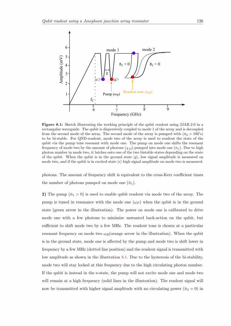
Qubit readout using a Josephson junction array resonator 126
Frequency (GHz)
6 7 8 9
fC
1
2
3
4
5
6
Am
plit
ude
(mV
)
mode 1 mode 2
n1 > 0 n1 = 0
Pump (P) Readout tone (R)
Figure 8.1: Sketch illustrating the working principle of the qubit readout using JJAR.2.0 in arectangular waveguide. The qubit is dispersively coupled to mode 1 of the array and is decoupledfrom the second mode of the array. The second mode of the array is pumped with (n2 > 100′s)to be bi-stable. For QND-readout, mode two of the array is used to readout the state of thequbit via the pump tone resonant with mode one. The pump on mode one shifts the resonantfrequency of mode two by the amount of photons (χ12) pumped into mode one (n1). Due to highphoton number in mode two, it latches onto one of the two bistable states depending on the stateof the qubit. When the qubit is in the ground state |g〉, low signal amplitude is measured onmode two, and if the qubit is in excited state |e〉 high signal amplitude on mode two is measured.
photons. The amount of frequency shift is equivalent to the cross-Kerr coefficient times
the number of photons pumped on mode one (n1).
2) The pump (n1 > 0) is used to enable qubit readout via mode two of the array. The
pump is tuned in resonance with the mode one (ωP ) when the qubit is in the ground
state (green arrow in the illustration). The power on mode one is calibrated to drive
mode one with a few photons to minimize unwanted back-action on the qubit, but
sufficient to shift mode two by a few MHz. The readout tone is chosen at a particular
resonant frequency on mode two ωR(orange arrow in the illustration). When the qubit
is in the ground state, mode one is affected by the pump and mode two is shift lower in
frequency by a few MHz (dotted line position) and the readout signal is transmitted with
low amplitude as shown in the illustration 8.1. Due to the hysteresis of the bi-stability,
mode two will stay locked at this frequency due to the high circulating photon number.
If the qubit is instead in the e-state, the pump will not excite mode one and mode two
will remain at a high frequency (solid lines in the illustration). The readout signal will
now be transmitted with higher signal amplitude with no circulating power (n2 = 0) in

Qubit readout using a Josephson junction array resonator 127
mode two.
8.2 Theory of a transmon qubit coupled to a JJAR.2.0
In this section I discuss the theory of a transmon qubit and the Hamiltonian of a JJA
coupled to a transmon qubit. The Hamiltonian of the system is given as follows
H = Hq + Harray + Hint (8.1)
The first and second term in the Hamiltonian 8.1 is the effective Hamiltonian of a
transmon qubit and a JJAR. The last term in the Hamiltonian is the interaction between
them.
8.2.1 Theory of a transmon qubit
The transmon consists of two superconducting islands separated by a Josephson junc-
tion [50]. The superconducting islands are designed such that the capacitive energy of
the circuit is lowered. In a circuit representation, depicted in figure 8.2, a large shunt
capacitance Csq is added in parallel to the Josephson junction. As a result the total ca-
pacitance is given by C∑ = CJq +Csq. Where CJq and Csq are the junction capacitance
and the shunt capacitance of a transmon qubit. The enhanced capacitance stabilises
charge fluctuations [50].
CSq CJq, LJq
a) b)Energy
|0
|1
Figure 8.2: a) Circuit representation of a transmon qubit. The cross in the box symbolisesthe non-linear inductance including the capacitance. The capacitance Csq is parallel to theJosephson junction in order to lower the capacitive energy EC of the transmon qubit. b) Thepotential energy of a transmon is periodic and has a cosine shape. Hence the quantized levelsare not equidistant in energy.

Qubit readout using a Josephson junction array resonator 128
A transmon qubit has a capacitive energy EC and a non-linear inductive EJ part. The
circuit for the transmon is shown in figure 8.2 [50]. The Hamiltonian of the circuit is
given as follows [50]
Hq =Q2
2C∑ − EJ cosφ. (8.2)
Where EJ is the Josephson energy, C∑ = CJq + CSq is the sum of capacitance’s. The
transmon qubit is an anharmonic oscillator and acts as a qubit for a weak drive strength,
with the transition frequency (~ωq) between ground and excited state. The properties of
the transmon are discussed in detail in [50]. For large EJ/EC the effective phase across
the junction is small. Thus we can approximate the cosine by a taylor expansion up to
fourth order. The taylor expanded eq. 8.2 is given as
Hq ≈Q2
2C∑ − EJ +EJ2φ2 − EJ
24φ4. (8.3)
The non-linear behaviour is still included in the fourth order term. The first three terms
approximate the cosine as a parabola describing a harmonic oscillator with a constant
energy shift Ej . The constant energy shift is neglected, because energy differences are
measured. The phase difference φ is connected to the flux variable Φ via φ = 2πΦΦ0
, hence
the charge and flux variable in equation 8.3 is replaced by the canonical conjugated
operators which are given as follows.
Φ ≈ i(b− b†),
Q ≈ (b+ b†)(8.4)
Where b† and b are the creation and annihilation operator, respectively. They satisfy
[b, b†] = 1. These operators are chosen such that they obey the canonical commutation
relation [Φn, Qn] = i. By substituting the canonical conjugate operators 8.4 in eq. 8.3.
The Hamiltonian eq. 8.3 is rewritten as follows
Hq = ~ω0b†b− e2
24C∑ (b− b†)4. (8.5)
ω0 is the transition frequency of the qubit between the ground and excited state. Expand-
ing (b − b†)4 and apply the first order perturbation theory and using the commutation

Qubit readout using a Josephson junction array resonator 129
relation [b, b†] = 1. The resulting Hamiltonian is
Hq = ~ω0b†b− EC
2(b†b)2 − EC b†b. (8.6)
The transmon is driven weakly such that only between lowest two energy levels are taken
into account with transition frequency ω0. The number operator b†b is replace by the
Pauli operator σz. The final Hamiltonian of the qubit is given by
Hq =~ωq2σz (8.7)
where ~ωq = ~ω0 − Ec. Since the transmon qubit is an anharmonic oscillator, the
anharmonicity α = E12 − E01 (where Eij is the energy difference between energy state
j and i) as shown in sketch 8.3, is measured by exciting the qubit at high power [188].
|g
|e
|f
g, e g, f
Figure 8.3: Energy transitions of the transmon qubit. On the left a dipole transition betweenthe ground |g〉 and the first excited state of the qubit |e〉 is shown. On the right a two photontransition between the ground |g〉 and the second excited state of the qubit |f〉 is shown. Theenergy difference between this energy state is α/2
This additional transition is a two photon transition. Two photons at a slightly lower
frequency (α/2) excite the second level of the qubit with low probability. Thus very
high power is used increasing the probability of two photon transition to happen. The
frequency difference between the single and two photon transition is used to obtain
information on the anharmonicity.
In the transmon regime [50] the anharmonicity α equals the charging energy α = −EC .
Since the qubit transition frequency ωq and the charging energy is known, the Josephson
energy EJ is calculated by
~ωq =√
8ECEJ − EC (8.8)

Qubit readout using a Josephson junction array resonator 130
8.2.2 Hamiltonian of JJAR.2.0
The electrical circuit of JJAR.2.0 is shown in figure 8.4a. The Lagrangian for the circuit
shown in 8.7a is given by
a)
0.3
0.0
-0.3
-0.1
0.2
0.1
-0.2
0 5 10 15
b)
25
20
15
5
0
10
0 2 4 6 8 10JJ # JJ #
Pha
se E
ighe
n F
unct
ion
Fre
quen
cy (
GH
z)
c)
CJ LJ
C0 C0'C0C0 C0 C0 C0
CJ LJ CJ LJ CJ LJ CJ LJ CJ LJ
Cs
x
Figure 8.4: JJAR.2.0. a) Electrical circuit representation of the JJAR.2.0, C ′0 is integratedat the center of the array without breaking the symmetry. b) show the eigen-phase for thefundamental mode (black dots) and second mode of the array (red dots) obtained from thenumerical simulations. The discrepancy due to influence of additional center ground capacitanceC ′0 is clearly visible on the 9th JJ. c) Dispersion relation for the circuit. The lowest mode ofthe array is influenced by the shunt capacitance(CS), C ′0 influence the even modes of the array,having the largest influence on the second mode of the array.
L =CS2
Φ20 +
C ′02
Φ2N/2 +
N−1∑x=1
(C0
2Φ2x
)+N−1∑x=0
Cj2
(Φx+1 − Φx)2
−N−1∑x=0
EJ
(1− cos
(2π
Φ0(Φx+1 − Φx)
))(8.9)
In order to transform to the Hamiltonian the conjugate momenta (charges) are derived
with respect to the node fluxes defined on the islands Φx
QN/2 =∂L
∂ΦN/2
= ΦN/2C0 + (ΦN/2 − ΦN/2−1)Cj + ΦN/2C′0 (8.10)

Qubit readout using a Josephson junction array resonator 131
Qx =∂L∂Φx
= ΦxC0 + (Φx − Φx−1)Cj − (Φx+1 − Φx)Cj (8.11)
Rewriting the charges in a matrix representation
~Q = C ~Φ (8.12)
With the derivative of the flux vector with respect to time (~ΦT = (Φ0, Φ1, ...., ΦN )) and
the capacitance matrix
C =
C0 + Cj + Cs −Cj 0 · · ·... 0
. . .. . .
. . .. . .
0 −Cj C0 + Cj + C ′0 −Cj 0 · · ·... 0
. . .. . .
. . .. . .
0 0... −Cj −Cj + C0
(8.13)
combined with the inverse of the inductance matrix
L−1 =
2LJ
−1LJ
0 · · ·... 0
. . .. . .
. . .. . .
0 −1LJ
2LJ
−1LJ
0 · · ·... 0
. . .. . .
. . .. . .
(8.14)
One can rewrite the Lagrangian of equation 8.9 as
L =1
2~ΦT C ~Φ− 1
2~ΦT L−1~Φ (8.15)
By performing the Legendre transformation using the momentum vector
~QT = (Q0, Q1, Q2, ..., QN ) (8.16)
to obtain the Hamiltonian of the Josephson junction chain in the linear limit
H = ~QT ~Φ− L = ~QT C−1 ~Q− 1
2~QT C−1 ~Q+
1
2~ΦT L−1~Φ
=1
2~QT C−1 ~Q+
1
2~ΦT L−1~Φ (8.17)

Qubit readout using a Josephson junction array resonator 132
Since the Hamiltonian is quadratic, it can be diagonalized and represented in the
form [51, 52]
H =1
2
N−1∑K=0
~ωKa†KaK (8.18)
By introducing the non-linearity of the Josephson junction as a perturbation the total
Hamiltonian of the JJA is given as follows (please refer to the theory chapter 2.5.2 for
detailed derivation).
Harray =∑j
~ω′j a†j aj −
∑j
~2Kjj(a
†j aj)
2 −∑j,k
(j 6=k)
~2Kjka
†j aj a
†kak (8.19)
Where Kjj and Kjk are the self and cross-Kerr coefficients.
8.2.3 Hamiltonian of total system
CJq, LJq
CSq
CJ LJ
C'0 C0
x
C0 C0C0C0C0
CJ LJ CJ LJ CJ LJ CJ LJ CJ LJ
Cs1 Cs2
CgCg
Figure 8.5: Circuit of a transmon qubit capacitively coupled to a Josephson junction arrayresonator which is loaded with an extra ground capacitance C ′0 and shunt capacitance CS1 andCS2. Cg is the coupling capacitance between the qubit and the array. As the transmon couplesonly symmetrically to the array and to the asymmetric odd modes (the coupling capacitance Cg
on left and right are the same).
The electrical circuit of our system is shown in figure 8.5. The interaction between a
transmon qubit and a single resonant cavity mode gives rise to the well known Jaynes-
Cummings Hamiltonian. The effective Hamiltonian of a JJAR coupled to a qubit is
given by equation 8.20 [50].
H =~ωq2σz+
∑j
~ω′j a†j aj−
∑j
~2Kjj(a
†j aj)
2−∑j,k
(j 6=k)
~2Kjka
†j aj a
†kak+~g(σ++σ−)(a1+a†1)
(8.20)
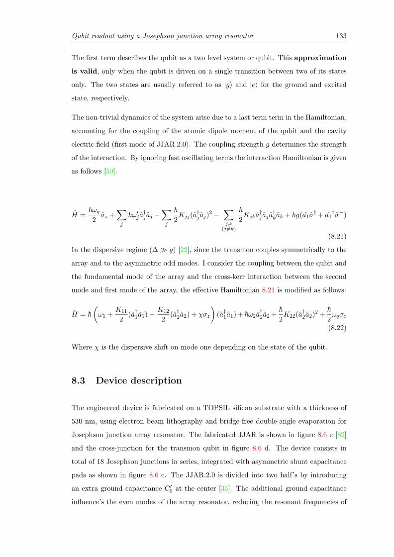
Qubit readout using a Josephson junction array resonator 133
The first term describes the qubit as a two level system or qubit. This approximation
is valid, only when the qubit is driven on a single transition between two of its states
only. The two states are usually referred to as |g〉 and |e〉 for the ground and excited
state, respectively.
The non-trivial dynamics of the system arise due to a last term term in the Hamiltonian,
accounting for the coupling of the atomic dipole moment of the qubit and the cavity
electric field (first mode of JJAR.2.0). The coupling strength g determines the strength
of the interaction. By ignoring fast oscillating terms the interaction Hamiltonian is given
as follows [50].
H =~ωq2σz +
∑j
~ω′j a†j aj −
∑j
~2Kjj(a
†j aj)
2 −∑j,k
(j 6=k)
~2Kjka
†j aj a
†kak + ~g(a1σ
† + a1†σ−)
(8.21)
In the dispersive regime (∆ g) [22], since the transmon couples symmetrically to the
array and to the asymmetric odd modes. I consider the coupling between the qubit and
the fundamental mode of the array and the cross-kerr interaction between the second
mode and first mode of the array, the effective Hamiltonian 8.21 is modified as follows:
H = ~(ω1 +
K11
2(a†1a1) +
K12
2(a†2a2) + χσz
)(a†1a1) + ~ω2a
†2a2 +
~2K22(a†2a2)2 +
~2ωqσz
(8.22)
Where χ is the dispersive shift on mode one depending on the state of the qubit.
8.3 Device description
The engineered device is fabricated on a TOPSIL silicon substrate with a thickness of
530 nm, using electron beam lithography and bridge-free double-angle evaporation for
Josephson junction array resonator. The fabricated JJAR is shown in figure 8.6 e [82]
and the cross-junction for the transmon qubit in figure 8.6 d. The device consists in
total of 18 Josephson junctions in series, integrated with asymmetric shunt capacitance
pads as shown in figure 8.6 c. The JJAR.2.0 is divided into two half’s by introducing
an extra ground capacitance C ′0 at the center [35]. The additional ground capacitance
influence’s the even modes of the array resonator, reducing the resonant frequencies of

Qubit readout using a Josephson junction array resonator 134
a)
d)
e)
m
m
Cg
50 W 50 W
IN OUT
Cg
CSq CJq
, LJqC0 C
J , LJ
Cs1
C'0+C0
C0
Cs2
b)
Wav
egui
dec)
mm
C'0 Cs2Cs1
CgCg
Figure 8.6: Device description. a) Photograph of one half of a rectangular waveguide witha 6 GHz cutoff. A JJA and a transmon qubit is fabricated on a piece of silicon substrate andplaced in the corner of the waveguide. b) Circuit representation of a transmon qubit coupledto a rectangular waveguide via a Josephson junction array. CS1, CS2 is the coupling capacitancebetween the JJA and the rectangular waveguide, Cg is the coupling capacitance between thequbit and JJA. c) Optical image of the JJAR.2.0 and a transmon qubit. d) Zoom-in SEMimage of a cross-junction design for transmon qubit. e) Zoom-in SEM image of a 9 Josephsonjunctions array.
the even modes. The parameters of the JJAR were designed such that the fundamental
frequency of the JJAR.2.0 combined with the shunt capacitance is around 6 GHz. The

Qubit readout using a Josephson junction array resonator 135
lowest two modes of the JJAR.2.0 are below 10 GHz and the spacing between the modes
is about 2 GHz. The plasma frequency of the JJAR.2.0 is around ωplasma ≈ 30 GHz.
The junctions in the array resonator were designed to have a large ratio of EJ/EC ≈ 313.
The sample is mounted in a rectangular waveguide with a cutoff frequency of 6 GHz.
The reason to have the sample off-center of the waveguide axes is to have the linewidth
of the resonant modes (κk) approximately equal to the anharmonicity (Kk). In this
regime the system show bi-stability at very few photons. Figure 8.6 b show the circuit
representation of the qubit coupled to the waveguide via a JJAR.2.0. A transmon qubit
is coupled capacitively (Cg) to the JJA resonator, and the JJA resonator is coupled
capacitively via the shunt capacitance pads (CS1, CS2) to the waveguide. Please refer to
Appendix B for the detail fabrication procedure of the sample.
8.3.1 Finite element simulations
1 mm2 mm 2 mm
a) b) c)
Figure 8.7: Finite element simulations: a) User-defined mesh on the device. The two redlines show where the two arrays of 9 Josephson junctions each are located. b) Electric fieldof the fundamental mode of JJAR.2.0 coupled to a transmon qubit. The electric field has itsmaximum intensity on the left and right pads of JJAR.2.0 with a minimum node at the center ofstructure, hence coupling strongly to the dipole of the qubit. c) Electric field of the second modeof JJAR.2.0 decoupled from transmon qubit. Electric field oscillate symmetric with respect tothe center of the JJAR.2.0, the gradient of field is perpendicular to the qubit, resulting in thequbit being decoupled from the second resonant mode of the array.
Fine tuning the parameters of a JJAR.2.0 geometry requires finite element simulations
with HFSS to find the correct parameter range for the resonance frequency of the modes
ωr(k), total capacitance of the structure (C∑) and the inductance (La) of the circuit.
Since the array consists in total of 18 junctions I assign the characteristic impedance

Qubit readout using a Josephson junction array resonator 136
for each junction to a lumped circuit element in HFSS (red color lines in figure 8.7 a)).
A fine mesh on the lumped elements is required to have accurate results. Figure 8.7 a)
show the user-defined mesh on a JJ array resonator. The centre capacitance pad is the
extra ground capacitance which reduce the resonant frequencies of the even modes. Due
to asymmetric shunt capacitance (CS1, CS2) pads both the odd and even modes of the
device couples efficiently to the waveguide.
Figure 8.7 b) show the magnitude and vector electric field (from finite element simu-
lations) for the fundamental mode of the device. The electric field has its maximum
intensity (red color) on the right and left pad and a node in the center of the device
representing a λ/2 resonator. The resulting gradient along the qubit pads enables the
coupling between the qubit and the fundamental mode. The voltage difference on the
qubit clearly show that the fundamental mode of the array can be used to excite the
qubit.
Figure 8.7 c) show the magnitude and vector electric field for the second mode of the
device. The maximum intensity of the electric field is at the left, the right, and the
middle pad of the resonator and the field is oscillating symmetrically with respect to
the center of the device. Since the resulting gradient of the field is perpendicular to the
qubit, the second mode of array is decoupled from the qubit.
8.4 Experimental results
The waveguide with the sample is mounted on the mixing chamber stage (10 mK) of
a cryogen free dilution refrigerator. The sample is enclosed in a double layer cryoperm
shield inside a completely closed copper can. The stainless steel input lines are atten-
uated with 20 dB at 4 K and 30 dB at base temperature. They are filtered with a
combination of a 12 GHz low pass and an Eccosorb filter. The output stage consists of
a 12 GHz low pass filter, two 4-12 GHz isolators and a 4-8 GHz HEMT amplifier. The
effective measurement bandwidth for direct transmission measurements using a VNA is
limited to about 4-9 GHz due to the cutoff of the waveguide and the combined bandwidth
of other microwave components.

Qubit readout using a Josephson junction array resonator 137
-2.5
-7.5
-12.5
-15-17.5
-5
-10
0
5.796 5.798 5.800 5.802 5.804 7.596 7.598 7.600 7.602
Frequency (GHz) Frequency (GHz)
|S21
| (dB
m)
|S21
| (dB
m)
a) b)
Qext = 12000Qint = 50000
Qext = 14000Qint = 30000
Figure 8.8: Transmission measurements, measured with a power corresponding to about onephoton circulating in the resonator. The solid line in the plot is a fit using Eq. 8.23 to extract Qtot
and ωR. a) Resonator response measurement for mode one. b) Resonator response measurementfor mode two.
8.4.1 Transmission measurements
Since the sample is capacitively coupled (CS1, CS2) to a rectangular waveguide as shown
in figure 8.6 a), it can be characterized by performing transmission measurements on the
waveguide using a VNA. The modified design of JJAR.2.0 couples both the odd and even
modes of the JJA to the waveguide. From the transmission S21 of the waveguide, the
resonant modes which are in the bandwidth of the experiment can be measured easily.
Two resonant modes out of 18 resonances of the array are shown in figure 8.8. The
measured raw data is further fitted with the following equation to extract the quality
factors of the resonances [43]
S21 = 1−1
Qext− 2i δffR
1Qtot
+ 2if−fRfR
. (8.23)
Where Qtot, Qext is the total and the coupling quality factor and δf takes into account
the impedance mismatch between the waveguide and the resonator. The fundamental
frequency of the JJAR is around 5.8 GHz with quality factors (Qint = 30000, Qext =
14000) and the second mode of the array is around 7.5 GHz with quality factors (Qint =
50000, Qext = 12000).

Qubit readout using a Josephson junction array resonator 138
8.4.2 Two-tone spectroscopy
-1-2 0-20
-15
-10
-5
0
5
8
10
6
4
2
R (MHz)
PD
(GH
z)
0 1-110
12
14
16
18 0
20a) b)
-20
-15
-10
-5
5
PD(G
Hz)
R(MHz)
Figure 8.9: Two-tone measurements. a) show the transmitted amplitude of the probe tonewith frequency ωR/2π = 5.799 GHz as a function of the pump tone frequency ωD
P and detuning∆R. When the pump tone frequency comes in resonance with the probe, the probe tone shiftsin frequency. The shift in probe frequency at ωD
P /2π = 5.799 GHz corresponds to self-kerrof the mode one. The frequency shift on the probe tone at ωD
P /2π = 7.599 GHz correspondsto the cross-kerr between mode one and on the mode two. b) As the device is intentionallyengineered to have the third resonant mode at around 30 GHz, there are no other shifts visibleup to bandwidth of the experimental setup which is 20 GHz. This is to cross check and calibratethe device.
From the direct transmission measurements on the waveguide, both the first mode and
the second mode of the JJA are measured using a drive power of a single photon in
the resonant modes. To characterize the device, I utilize a two-tone spectroscopy mea-
surement to find other resonant modes of the array, to cross check there are no other
resonances up to bandwidth of the experimental setup which is 20 GHz. Figure 8.9 a),
b) show the results of a two-tone spectroscopy measurement, where the frequency is
swept from 0 to 20 GHz with a constant pump tone while weakly probing the funda-
mental mode ωR/2π = 5.799 GHz of the array with a VNA. By comparing the measured
frequencies of the entire JJA with the re-normalized mode frequencies calculated by di-
agonalizing the capacitance matrix (Appendix A), the JJA parameters can be extracted
C0 = 0.152 fF, CJ = 30 fF, LJ = 0.755 nH, CS = 85 fF and C ′0 = 255 fF.
8.4.3 Kerr measurements
The Kerr effect manifests itself as a frequency shift that depends linearly on the number
of photons in a resonant mode [52, 51, 44]. By varying the input power on a low signal

Qubit readout using a Josephson junction array resonator 139
level and measuring the frequency shift, we can measure the Kerr shift per photon.
Figure 8.10 show the self-Kerr measurement on mode one and mode two of the JJA.
The input power is converted into a mean photon number using equation 8.24 [51].
n =2Q2
tot
~ω2kQext
Pin (8.24)
Here ωk is the resonance frequency of a particular mode, Qtot is the total quality factor,
Qext is the coupling quality factor and Pin is the input signal power. Further by fitting
the measured data with a third order polynomial, the anharmonicity of each mode can
be extracted.
8.4.3.1 Self- Kerr measurement
For the self-Kerr measurements only one mode i of the chain is excited. Further mea-
suring the frequency shift ∆P with respect to the input power using direct transmission
measurements. Each data-set is fitted with a notch type response function to extract
the frequency ωi and Qi,tot. From the shift relative to the bare resonance frequency the
self-Kerr coefficient Ki is extracted.
1 (
MH
z)
D2
(kH
z)
a) b)0.0
-0.2
-0.4
-0.6
-0.8
-1.0
20 40 60n
0.0
-0.2
-0.4
-0.6
-0.8
-1.0
-1.2
-1.4
2 (
MH
z)
5 10 15 20n
K1 = 59.2 kHz/Photon K2 = 120.7 kHz/Photon
Figure 8.10: Self-Kerr measurements. a) Dependence of the self-Kerr frequency shift on thephoton number of mode one. The red line is a third order polynomial fit. b) Dependence ofthe self-Kerr frequency shift on the photon number of mode two. The red line is a third orderpolynomial fit.

Qubit readout using a Josephson junction array resonator 140
Figure a, b show the self-Kerr measurements on mode one and mode two of the JJAR.2.0.
For low input power P , the ∆i changes linearly with power. For high input power, higher
order non-linearity terms (K ′1,K′′1 ) start to play a role. To take this into account the
data is fitted with the following dependence.
∆i(n) = K1n+K ′12n2 +
K ′′13n3 (8.25)
Here K ′1,K′′1 corresponds to the higher order non-linear terms. Thus extracting the Kerr
coefficients in units of Hz/Photon.
8.4.3.2 Cross-kerr measurements
For determining the cross-Kerr coefficients Kij , I utilize two-tone spectroscopy measure-
ments [52, 43]. Mode 1 of the array is used as the readout with a power of about one
photon and mode 2 is excited with varying power and vice-versa. From the shift ∆R of
the resonance frequency of the readout mode ωR/2π upon application of a pump tone,
the cross-Kerr shift Kij can be extracted.
Figure 8.11 a show a typical two-tone spectroscopy measurements to extract the cross-
Kerr coefficient K12 by pumping mode two and observing the frequency shift on mode
one. Mode one is driven at a constant readout strength of n1 < 1 photons. To extract
the maximal frequency shift ∆1, each pump frequency is fitted to a notch type response
function 8.23 and the resonance frequency(solid black line) is extracted. The maximal
shift of the readout resonator for a given pump power results in one data point in
Figure 8.11 b), c), d). From the measurement in figure 8.11 c one can also clearly
observe that the mode becomes bistable at a few hundred’s of photons.
Figure 8.12 a), b) show the result of all two tone measurement to determine the cross-
Kerr shift K12 when driving mode two and using mode one as the readout and K21
when driving mode one and using mode two as the readout [51]. For low input power,
∆21 changes linearly with the power but then rapidly higher order terms come into
play. Hence the data is fitted to a third order polynomial. From the fit, the cross-Kerr
coefficient can be extracted as K12, K21 = 49 KHz/Photon. By inserting the measured
values of self-Kerr coefficients of the mode one and the mode two of the JJAR.2.0 in the
theoretical formula (1/√
2√K11K22), I find an agreement within 20 %.

Qubit readout using a Josephson junction array resonator 141
-2-4 0
0
50
-6
-4
-2
-6-8
0
-4
-2
2
-2-4 0-6
0
-4
-2
2
4
-2 -1.5 -1 -0.5 0R (MHz)
P (M
Hz) 0
-4
-2
2
-2-4 0-6
a) b)
c) d)
P(M
Hz)
R(MHz)
P(M
Hz)
R(MHz)
P(M
Hz)
R(MHz)
Figure 8.11: Cross-Kerr measurements K12. a), b), c), d) Two-tone spectroscopy measure-ments for different pump strength. Shift ∆R of the resonance frequency of the readout modeωR/2π = 5.799 GHz with nR = 1 photons upon application of a pump tone to mode twoof JJAR.2.0. The pump frequency is detuned by ∆P from the resonance of the second modeωP /2π = 7.599 GHz. a), b), c), d) Corresponds to different number of photons ≈ 8, ≈ 35,≈ 230 and ≈ 400 photons in the pump mode.
The measured Kerr coefficients of the device for mode one and mode two of device is
summarized in the table below and compared to the analytical calculations obtained by
diagonalizing the capacitance matrix (refer to appendix A).
The measured anharmonicities(α2) of the JJAR.2.0 resonant modes is not equal to the
linewidth(κ2) of the resonant mode, thus bi-stability on second mode appears at a few
hundred’s of photons . This is mainly due to influence of the linear geometric inductance
coming from the Josephson junctions and the connecting wires of array shown with green
color in figure 8.13 b).

Qubit readout using a Josephson junction array resonator 142
b)
n2n1
12 (
MH
z)
21(
MH
z)
a)
200 400
Figure 8.12: Summary of Cross-Kerr measurement. a) Cross kerr measurement, where modeone of the arrays is pumped and mode two of the array is used to readout the frequency shift. b)Mode two of the arrays is pumped and mode one of the array is used to readout the frequencyshift. The red line is a third order polynomial fit.
Mode ωi/2π Qint Qext Qtot κi Ki Ki2 Ki(Theory) Ki2(Theory)(GHz) (kHz) (kHz) (kHz) (MHZ) (MHz)
1 5.799(3) 30000 14000 10680 543 59.2 49 6.247 6.755
2 7.599(3) 50000 12000 9364 811.5 120.7 - 7.35 -
Table 8.1: Parameters for the two modes of JJAR.2.0 that can be directly measured with theVNA. fr and Qtot were extracted from data. The Kerr and cross-Kerr coefficients are calculatedfrom a fit to the polynomial fit as shown in the Fig. 8.12, 8.10.
8.4.4 Influence of the geometric inductance
The measured Kerr non-linearities of the JJAR.2.0 are low compared to the numerical
calculations given in table 8.1. This is due to not taking into account the influence
of linear inductance present in the circuit 8.13 a). The geometric inductance influences
the participation ratio of JJAR.2.0, resulting in lower non-linearities. The geometric
inductance of a thin film wire is calculated with the following equation [189].
LP = 2 ∗ 10−3 ∗ l ∗[ln
(2.0 ∗ lw + t
)+ 0.5 + 0.2235
(w + t
l
)]µH (8.26)
Where l, w, t is the length, width and thickness in cm. In addition to Josephson
inductance LJ = 0.755 nH, the JJAR is mostly influenced by the geometric inductance
of thin films arising from thin wires of the Josephson junctions (green lines shown in
figure 8.13 b)) which is around LP = 0.18 nH (calculated from equation 8.26). The
additional geometric linear inductance is in series to the Josephson inductance. Hence

Qubit readout using a Josephson junction array resonator 143
CJq, LJq
CSq
CJ LJ
C'0
x
C0C0C0
CJ LJ CJ LJ
Cs1 Cs2
a)
C'0
LP LP LP LP
b) Cg
1 m
Cg
Figure 8.13: a) Electric circuit representing the influence of geometric linear inductance (LP )arising from Josephson junction array resonator coupled to a transmon qubit. b) Zoom-in SEMimage, total of 18 Josephson junctions array divided into two half’s with additional groundcapacitance (C ′0) at the center. The green lines on the Josephson junctions contribute the extralinear distributed geometric inductance (LP ).
the circuit diagram 8.5 is modified with an additional linear inductance in series to each
Josephson junction as shown in figure 8.13 a). By adding the linear inductance (LP ) to
the numerical calculations, I find an agreement of the measured anharmonicity within
28%.
In order to reduce the geometric inductance, it is important to reduce the Josephson
junction length and increase the width of the Josephson junctions. By doing this the
Josephson inductance will be kept constant and reduce the geometric inductance of the
thin films. The plan for the future device is to reduce the effect of linear inductance
arising from thin film of the Josephson junction.
8.4.5 Qubit measurements
The transmon qubit in our design is perpendicular to electric field of the waveguide.
Hence the qubit is decoupled from the waveguide. Since the transmon is designed sym-
metrically to the JJAR.2.0, thus it only coupled to the asymmetric odd modes of the
array and decoupled from the even modes. The fundamental mode of the JJAR.2.0 is
dispersively coupled to the qubit and is used to drive the qubit. The optical image of
the transmon qubit coupled to the JJAR.2.0 is shown in figure 8.6 c).

Qubit readout using a Josephson junction array resonator 144
The transmon qubit in this case is 1.2 mm long with an inductance of Lq = 19 nH
and a total capacitance of a few tens of fF ’s. The asymmetric pads of the JJAR.2.0
shown in figure 8.6 c) allow the qubit to couple strongly to the fundamental mode of the
array. Hence the information about the state of a qubit can only be readout using the
fundamental mode of the JJAR.2.0. By utilizing two-tone spectroscopy measurement it
is possible to determine the transition frequency of the qubit.
R(MHz)
Gen
erat
or f
requ
ency
(GH
z)
R(MHz)
R(MHz)
a) b)
Figure 8.14: a) Two-tone spectroscopy measurement: The transmitted amplitude of the read-out mode one of the JJAR.2.0 with frequency ωR/2π =5.799 GHz as a function of the signal gen-erator frequency and detuning ∆R. b) High power excitation measurement. Exciting the qubitat high power reveals a transition to the second excited state at a frequency of 3.647(4) GHz.
Figure 8.14 a) show the two tone measurement on the qubit. Since the qubit is coupled
only to mode one of the JJAR.2.0. I utilize a two-tone spectroscopy measurement to
measure the transition frequency of the qubit. The frequency of the pump tone is swept
around the qubit frequency, while weakly probing mode one with the VNA. When the
pump tone is resonant with the qubit transition frequency, the resonance frequency of
mode one shift as shown in figure 8.14 a).
From the measurement the transition frequency of the qubit is ωq/2π = 3.768(4) GHz.
The initial qubit design is intended to have a transition frequency around 5 GHz. The
frequency of the transmon qubit is off by about 1 GHz compared to the finite element
simulations. This is due to a wrong estimate of the superconducting energy gap ∆
(estimated ∆ = 210 eV) of our Aluminium(Al) material. It turned out that the energy
gap of our superconducting Al material used for fabricating the device is about 165 eV,
hence effecting the Josephson inductance of transmon qubit.

Qubit readout using a Josephson junction array resonator 145
The anharmonicity of the qubit is measured by exciting the qubit at high power. Due
to the high power an additional transition appears as shown in figure 8.14 b), exciting
the qubit’s next higher state. The additional transition is a two photon transition. The
difference between the single and the two photon transition is used to gain information
on the anharmonicity of the qubit. The characterized parameters of the qubit are given
in the table below.
Parameter Value Error HFSS HFSS(with superconducting (with superconducting
gap(∆) =210 eV) gap(∆) =165 eV)
Qubit frequency (GHz) 3.7681 2e-5 5.08 4.1351
Anharmonicity (MHz) 241.4 0.2 261.5 248.43
Chi (MHz) 0.8 0.08 1.8 1.17
LJ (nH) 19.77 0.02 13 19
g(MHz) 78.17 0.05 94.5 125.7
EJ (GHz) 8.268 0.007 12.5 8.603
EJ/EC 34.25 0.06 48.95 34.62
Table 8.2: Parameters of the transmon qubit characterized using the fundamental mode ofJJAR. 2. 0. The theory parameters mentioned in the last two column are obtained from black-box quantization simulations considering different superconducting gap for Aluminium (∆) [118].
8.5 Conclusion
In conclusion, I have successfully engineered, fabricated and characterized a novel de-
vice for qubit readout. Due to the time constraints the pulse measurements and phase
measurements on the qubit are currently on-going work in collaboration with my col-
league. The device is engineered to have an anharmonicity of the JJA resonant modes
approximately equal to the linewidth of a particular resonant modes of a JJA. Such that
the bi-stability appears at very few photons. However, due to the influence of geometric
inductance of Josephson junction thin films and anharmonicities of the device are re-
duced by a factor of 10 compared to the linewidth of a particular resonant modes. The
future plans is to improve the coupling of a JJAR.2.0 to the waveguide by placing it at
the center of the waveguide, and to reduce the geometric inductance of JJAR.2.0, hence
should be able to utilize the engineered two mode system for good qubit readout.

Chapter 9
Conclusion
This experimental work in this thesis consists of three main accomplishments.
The first part was designing and building a 3D circuit QED setup from scratch in a
new lab which involved the following main steps: producing high quality factor cavities;
designing, building and installing the cryogenic microwave setup as well as the room
temperature amplification chains.
The second part was the finite element numerical simulations, utilizing the naturally
occuring dipolar interactions in 3D superconducting circuits to realize a platform for
analogue quantum simulation of XY spin models. The possibility of realizing arbitrary
lattice geometries with locally-tunable dipole moments [29], in combination with their
large interaction strength, opens the door to the investigation of a series of phenomena in
quantum magnetism in both 1D [121, 122] and 2D [106], complementing the remarkable
developments in cold atom and trapped ion systems [96, 97, 98]. The idea discussed in
chapter 5 are not limited to Transmon qubits, but could be implemented with, e.g., Xmon
qubits [89] or Fluxonium qubits coupled to an antenna [123]. It would be interesting to
explore these developments in view of realizing Hamiltonian dynamics for surface code
architectures [8] or as a building block for coupled cavity array experiments [124, 125].
High Q resonators are important for a qubit readout. A design for MSRs with a low
interface participation ratio embedded in a rectangular waveguide is engineered and
characterized. The presented setup, is an ideal platform for implementing interacting
spin systems [91, 29] where the MSR can be used for readout. In Fig. 9.1 shows a
conceptual schematic for simulating spin chain physics. The orientation of the qubits
146

Conclusion 147
Figure 9.1: MSRs used for analog quantum simulation. Conceptual schematic of arectangular waveguide setup using three MSRs as a readout for a chain of transmon qubits.The transmon qubits couple capacitively to each other to realize a system for analog quantumsimulation of spin chain physics.
relative to the waveguide allows us to control the coupling of the qubits to the waveguide
mode. Fig. 9.1 they are oriented along the axis of the waveguide which will lead to a
large qubit-qubit interaction but negligible coupling to the waveguide. Three MSRs
with different frequencies, all above the waveguide’s cutoff, are used to read out selected
qubits. Another interesting aspect of the setup mentioned in chapter 6 is the built-in
protection from spontaneous emission due to the Purcell effect, similar to [74, 190] but
broadband. Even though the qubit is strongly coupled to the resonator it can not decay
through the resonator, as the waveguide acts as a filter if the qubit frequency is below
the cutoff. This platform can also be used to investigate the interplay between short
range direct interactions, long range photon mediated interaction via the waveguide [191]
and dissipative coupling to an open system. It offers a new route to investigate non-
equilibrium condensed matter problems and makes use of dissipative state engineering
protocols to prepare many-body states and non-equilibrium phases [192, 193].
The third part consists of exploring physics in the mesoscopic regime using a JJAR. The
device exhibits bi-stability at very few photons, this is achieved by engineering the Kerr
interaction strength to be comparable to the linewidth. This proof of principle device
demonstrates that it is possible for a few microwave photons in the readout mode to
switch the photon occupation number by two orders of magnitude in the pump mode.
As such it is a promising system to implement novel types of nondemolition measure-
ments [194], single photon microwave transistors [195, 196], single photon microwave
switches [197], Flip-Flop memories [198] or even elements for autonomous quantum er-
ror correction [154].
In the last chapter of this thesis, a modified JJAR.2.0 is designed and characterized

Conclusion 148
for dispersive readout on the qubit. The principle idea of JJAR.2.0 is to exhibit bi-
stability at a few photons. This can be achieved by engineering a device which will have
anharmonicites equal to the linewidth of the resonant modes. The fundamental mode of
the JJAR.2.0 is used to dispersively readout the state of a qubit with very few photons.
However, the measured device has a geometric inductance LP ≈ 0.1 nH arising from
the Josephson junctions and the connecting wires between the junctions is on the same
order of the Josephson inductance LJ ≈ 0.755 nH. Hence decreasing the anharmonicites
by factors of 10 compared to the line-width of a particular resonant modes.

Appendix A
Mathematica code :JJAR.2.0
149

In[498]:= ClearAll["Global`*"];
c = 3 * 10^8;
mu0 = 4 * Pi * 10^(-7);
eps0 = 8.8 * 10^-12;
ele = 1.6 * 10^-19;
h = 6.626068 * 10^-34;
hBar = h 2 * Pi;
delta = 165 * ele * 10^-6;
kB = 1.3806503 * 10^-23;
T = 20 * 10^-3; (* temperature in K*)
NN = 19; (*num juncs +1 *)
L, σL = 0.755, 0.00; (* 10-9, σL is in fractional ie 0.03= 3% ;
also, see below for "one messed up junction"*)
Cs = [email protected];(*10-15*) (*Sets ground mode freq*)
Cj = [email protected];(*10-15;*) (*Sets plasma freq with Lj*)
C0 = 0.150; (* 10-15 Brings dispersion down *)
Junc_σ = If[σL ⩵ 0, 1, RandomVariate[NormalDistribution[1, σL], NN - 1]];
Ljs = N[Junc_σ] * ConstantArray[L, NN - 1];
Ljs[[1 ;; 18]] = Ljs[[1 ;; 18]] * 1;
LMi = DiagonalMatrixPrependLjs^-1, 0;
CjM = DiagonalMatrixPrependConstantArray[Cj, NN - 1] Junc_σ, 0;
MatrixForm[CjM];
CsM = N[Normal[SparseArray[i_, j_ /; i ⩵ j && i ⩵ 1 → 1, NN, NN]] +
ConstantArray[1, NN, NN]];
CsM1 = N[Normal[SparseArray[2, 2 → 1, NN, NN]]];
MatrixForm[CsM1];
CsMid = N[Normal[SparseArray[10, 10 → 1, NN, NN]]];
MatrixForm[CsMid]
CsM = CsM + 8.4 * CsMid;
C0M = N[Normal[SparseArray[i_, j_ /; i ⩵ j && i ⩵ 1 → NN - 2,
i_, j_ /; i ≠ NN && j ≠ NN → NN - Max[i, j], NN, NN]]];
MatrixForm[C0M];
C0M = NNormalSparseArrayi_, j_ → NN + 1 - Max[i, j], NN, NN;
CM = CjM + Cs * CsM + C0 * C0M 10^6;
CMi = Inverse[CM];
evals, evecs = N[Eigensystem[CMi.LMi]];
IfAbs[evals[[-1]] + 0] > 10^-6,
MessageDialog["Warning! The smallest eigenvalue was not 0!"];
evecs = Normalize /@ evecs;
evals = Reverse[evals]; evecs = Reverse[evecs];
EF = evals; EV = evecs;
evals = evals[[2 ;; -1]]; evecs = evecs[[2 ;; -1, 2 ;; -1]];
evecs = If[#1[[1]] > 0, #1, -#1] & /@ evecs;
freqs = Sqrt[evals] 2 * Pi;

freqs, evecs;
EjGHz[Lq_] := hBar 2 ele^2 h (Lq);
Norms = 2 * Diagonal[EV.LMi.EV];
(*RMS norm*)Norms[[1]] = 1;
(*just to avoid avoid division by zero;
this value will still correspond to zero for the DC mode*)
PJs = Prepend[Ljs^-1, 0] * #^2 & /@ EV (Norms);
(*Matrix of PJs for each mode and for each junction*)
(*The "prepend 0" is there to deal with the DC mode,
which we will remove in the next line*)
= PJs[[2 ;; -1, 2 ;; -1]] (*get rid of DC mode and DC node with no JJ.*);
= DiagonalMatrixFR = Sqrt[EF[[2 ;; -1]]] 2 π
(*undressed freqs,the same as abouve*);
ji = DiagonalMatrix[(EjGHz /@ Ljs)^-1];
X = ..ji.. 2(*in GHz*);
χ1 = #, 10^3 X[[1, #]] & /@ Range[8];
(*in MHz*)χ3 = #, 10^3 X[[3, #]] & /@ Range[8];
(*in MHz*)alpha = #, 10^3 X[[#, #]] & /@ Range[8];
Print["Plasma frequency: Subscript[f, 0] = ", FR[[-1]], " GHz"];
Print["The first mode: Subscript[f, 1] = ", FR[[1]], " GHz"];
Print[
"The anharmonicity of a junction alone (plasma mode): Subscript[α, 0] = ",
X[[8, 8]] * 10^3, " MHz"];
Print["The anharmonicity of mode 1 (", FR[[1]],
" GHz): Subscript[α, 1] = ", X[[1, 1]] * 10^3, " MHz/photon ;"];
Print["The anharmonicity of mode 2 (", FR[[2]],
" GHz): Subscript[α, 2] = ", X[[2, 2]] * 10^3, " MHz/photon ;"];
Print["The anharmonicity of mode 2 (", FR[[3]],
" GHz): Subscript[α, 2] = ", X[[3, 3]] * 10^3, " MHz/photon ;"];
Print["The cross-Kerr of mode 1 and 1:Subscript[χ, 1,2] = ",
X[[1, 2]] * 10^3, " MHz"];
ListPlot(*MeasFr,*)FR[[1 ;; 10]],
PlotStyle → Directive[PointSize[0.015], Darker[Red, 0.2]],
Directive[PointSize[0.012], Blue], AspectRatio → 1 1,
ImageSize → 300, Axes → False, Frame → True, FrameStyle → Thick,
LabelStyle → Directive[FontSize → 12, FontFamily → "Arial", FontSlant → "Plain"],
FrameLabel → "mode #", "Frequency (GHz)"
ListPlotalpha[[1 ;; 8]],
PlotStyle → Directive[PointSize[0.015], Darker[Red, 0.2]],
Directive[PointSize[0.012], Blue], AspectRatio -> 1 1,
ImageSize → 300, Axes → False, Frame → True, FrameStyle → Thick,
LabelStyle → Directive[FontSize → 25,
FontFamily → "Arial", FontSlant → "Plain"],
FrameLabel → "mode #", "anharmonicity (α) (MHz)"
2 JJAR.2.0.nb

Plasma frequency: Subscript[f, 0] = 33.42 GHz
The first mode: Subscript[f, 1] = 5.94475 GHz
The anharmonicity of a junction alone (plasma mode): Subscript[α, 0] = 70.4634 MHz
The anharmonicity of mode 1 (5.94475 GHz): Subscript[α, 1] = 6.24752 MHz/photon ;
The anharmonicity of mode 2 (7.51134 GHz): Subscript[α, 2] = 7.35093 MHz/photon ;
The anharmonicity of mode 2 (31.0183 GHz): Subscript[α, 2] = 46.1776 MHz/photon ;
The cross-Kerr of mode 1 and 1:Subscript[χ, 1,2] = 6.75565 MHz
Out[553]=
0 2 4 6 8 100
5
10
15
20
25
30
35
mode #
Frequency
(GHz)
Out[554]=
0 2 4 6 8010203040506070
mode #
anharmonicity
(α)(MHz)
JJAR.2.0.nb 3

Appendix B
Fabrication recipe
153

Appendix B 154
Step Description Equipment used Precision
1 Cleaving 4 inch Diamond cutting tool 4-inch wafer issubstrate cleaved into 4 quarter’s
2 Cleaning Acetone Ultrasonic bath for 15 minsIsopropanal Ultrasonic bath for 10 mins
Distilled water Rinse in DI waterfollowed by blow dry using N2
3 Resist coating MMA(8.5) MAA EL 13 Spin 40 s at 500 rpm,(copolymer) Spin 60 s at 1500 rpm
Baking on hot plate at200 for 5 min
4 Resist coating PMMA 950k Spin 100 s at 2000 rpmBaking at 200 for 5 min
5 E-beam lithography Reith 30 keV Acceleration voltage 30 KVBig aperture:
Beam current 5.5 nALarge area doses 360 µC/cm2
Small aperture:Beam current 36.5 pA
Junction dose 600 µC/cm2
Undercut dose 160 µC/cm2
6 Development IPA:water 1:3 105 s at 6
5 s in DI waterN2 blow dry, low pressure
7 Al deposition Plassys 25 nm at 1 nm/s and 25
-MEB550SOxidation 10 mBar
for 1 min30 nm at 1 nm/s amd −25
8 Lift-off Acetone 4 hours at 60 CRinse in IPA, DI
Blow dry N2
Table B.1: Fabrication recipe for Josephson junctions.

Bibliography
[1] Eleanor Rieffel and Wolfgang Polak. Quantum computing: a gentle introduction.
The MIT Press, 2011.
[2] Peter W. Shor. Polynomial-Time Algorithms for Prime Factorization and Discrete
Logarithms on a Quantum Computer. SIAM Journal on Computing 0097-5397,
26(5):1484–1509, October 1997.
[3] Lieven M. K. Vandersypen, Matthias Steffen, Gregory Breyta, Costantino S. Yan-
noni, Mark H. Sherwood, and Isaac L. Chuang. Experimental realization of Shor’s
quantum factoring algorithm using nuclear magnetic resonance. Nature., 1476-
4687, 414(6866):883–887, December 2001.
[4] M. Gilowski, T. Wendrich, T. Muller, Ch. Jentsch, W. Ertmer, E. M. Rasel, and
W. P. Schleich. Gauss sum factorization with cold atoms. Phys. Rev. Lett., 100:
030201, Jan 2008.
[5] Alberto Politi, Jonathan C. F. Matthews, and Jeremy L. O’Brien. Shor’s quantum
factoring algorithm on a photonic chip. Science.,0036-8075, 325(5945):1221–1221,
2009.
[6] Thomas Monz, Daniel Nigg, Esteban A. Martinez, Matthias F. Brandl, Philipp
Schindler, Richard Rines, Shannon X. Wang, Isaac L. Chuang, and Rainer Blatt.
Realization of a scalable shor algorithm. Science.,0036-8075, 351(6277):1068–1070,
2016.
[7] Erik Lucero, R. Barends, Y. Chen, J. Kelly, M. Mariantoni, A. Megrant,
P. O’Malley, D. Sank, A. Vainsencher, J. Wenner, T. White, Y. Yin, A. N. Cleland,
and John M. Martinis. Computing prime factors with a Josephson phase qubit
quantum processor. Nature Physics, 8(10):719–723, October 2012.
155

Bibliography 156
[8] Austin G. Fowler, Matteo Mariantoni, John M. Martinis, and Andrew N. Cleland.
Surface codes: Towards practical large-scale quantum computation. Phys. Rev. A,
86:032324, Sep 2012.
[9] Ryan Babbush, Jarrod McClean, Dave Wecker, Alan Aspuru-Guzik, and Nathan
Wiebe. Chemical basis of trotter-suzuki errors in quantum chemistry simulation.
Phys. Rev. A, 91:022311, Feb 2015.
[10] Tadashi Kadowaki. Study of Optimization Problems by Quantum Annealing. PhD
thesis, 1998.
[11] Roman Orus, Samuel Mugel, and Enrique Lizaso. Quantum computing for finance:
Overview and prospects. Reviews in Physics 2405-4283, 4:100028, November 2019.
[12] Javier Arguello-Luengo, Alejandro Gonzalez-Tudela, Tao Shi, Peter Zoller, and
J. Ignacio Cirac. Analogue quantum chemistry simulation. Nature.,0028-0836,
1476-4687, 574(7777):215–218, October 2019.
[13] Maria Schuld, Ilya Sinayskiy, and Francesco Petruccione. The quest for a Quantum
Neural Network. Quantum Information Processing1573-1332, 13(11):2567–2586,
November 2014.
[14] Chih-Chun Chien, Michael Zwolak, and Massimiliano Di Ventra. Bosonic and
fermionic transport phenomena of ultracold atoms in one-dimensional optical lat-
tices. Phys. Rev. A, 85:041601, Apr 2012.
[15] Daniel Greif, Thomas Uehlinger, Gregor Jotzu, Leticia Tarruell, and Tilman
Esslinger. Short-Range Quantum Magnetism of Ultracold Fermions in an Optical
Lattice. Science.,0036-8075, 1095-9203, 340(6138):1307–1310, June 2013.
[16] Markus Greiner, Olaf Mandel, Tilman Esslinger, Theodor W. Hansch, and Im-
manuel Bloch. Quantum phase transition from a superfluid to a Mott insulator in
a gas of ultracold atoms. Nature., 1476-4687, 415(6867):39–44, January 2002.
[17] Tim Byrnes, Na Young Kim, Kenichiro Kusudo, and Yoshihisa Yamamoto. Quan-
tum simulation of fermi-hubbard models in semiconductor quantum-dot arrays.
Phys. Rev. B, 78:075320, Aug 2008.
[18] A. Friedenauer, H. Schmitz, J. T. Glueckert, D. Porras, and T. Schaetz. Simulating
a quantum magnet with trapped ions. Nature Physics, 4:757–761, October 2008.

Bibliography 157
[19] Y. Salathe, M. Mondal, M. Oppliger, J. Heinsoo, P. Kurpiers, A. Potocnik, A. Mez-
zacapo, U. Las Heras, L. Lamata, E. Solano, S. Filipp, and A. Wallraff. Digital
quantum simulation of spin models with circuit quantum electrodynamics. Phys.
Rev. X, 5:021027, Jun 2015.
[20] B. D. Josephson. Possible new effects in superconductive tunnelling. Physics
Letters ., 1(7):251–253, July 1962. ISSN 0031-9163.
[21] Herbert Simanjuntak and Leon Gunther. Macroscopic quantum tunneling in un-
shunted Josephson junctions. Journal of Low Temperature Physics1573-7357, 78
(1):131–139, January 1990.
[22] Alexandre Blais, Ren-Shou Huang, Andreas Wallraff, S. M. Girvin, and R. J.
Schoelkopf. Cavity quantum electrodynamics for superconducting electrical cir-
cuits: An architecture for quantum computation. Phys. Rev. A, 69:062320, Jun
2004.
[23] M. H. Devoret and R. J. Schoelkopf. Superconducting Circuits for Quantum Infor-
mation: An Outlook. Science.,0036-8075, 1095-9203, 339(6124):1169–1174, March
2013.
[24] Gary J. Mooney, Charles D. Hill, and Lloyd C. L. Hollenberg. Entanglement in a
20-Qubit Superconducting Quantum Computer. Scientific Reports.,2045-2322, 9
(1):1–8, September 2019.
[25] Flora Graham. Daily briefing: Google’s quantum-supremacy paper is here. Tech-
nical report, October 2019.
[26] M. D. Reed, L. DiCarlo, S. E. Nigg, L. Sun, L. Frunzio, S. M. Girvin, and R. J.
Schoelkopf. Realization of three-qubit quantum error correction with supercon-
ducting circuits. Nature.,1476-4687, 482(7385):382–385, February 2012.
[27] L. DiCarlo, J. M. Chow, J. M. Gambetta, Lev S. Bishop, B. R. Johnson, D. I.
Schuster, J. Majer, A. Blais, L. Frunzio, S. M. Girvin, and R. J. Schoelkopf.
Demonstration of two-qubit algorithms with a superconducting quantum proces-
sor. Nature.,1476-4687, 460(7252):240–244, July 2009.

Bibliography 158
[28] Brian Vlastakis, Gerhard Kirchmair, Zaki Leghtas, Simon E. Nigg, Luigi Frunzio,
S. M. Girvin, Mazyar Mirrahimi, M. H. Devoret, and R. J. Schoelkopf. Deter-
ministically Encoding Quantum Information Using 100-Photon Schrodinger Cat
States. Science.,0036-8075, 1095-9203, September 2013.
[29] M. Dalmonte, S. I. Mirzaei, P. R. Muppalla, D. Marcos, P. Zoller, and G. Kirch-
mair. Realizing dipolar spin models with arrays of superconducting qubits. Phys.
Rev. B, 92:174507, Nov 2015.
[30] Hanhee Paik, D. I. Schuster, Lev S. Bishop, G. Kirchmair, G. Catelani, A. P.
Sears, B. R. Johnson, M. J. Reagor, L. Frunzio, L. I. Glazman, S. M. Girvin,
M. H. Devoret, and R. J. Schoelkopf. Observation of high coherence in josephson
junction qubits measured in a three-dimensional circuit qed architecture. Phys.
Rev. Lett., 107:240501, Dec 2011.
[31] Chanchal K. Majumdar and Dipan K. Ghosh. On Next-Nearest-Neighbor In-
teraction in Linear Chain. I. Journal of Mathematical Physics0022-2488, 10(8):
1388–1398, August 1969.
[32] Christian Kraglund Andersen, Archana Kamal, Nicholas A. Masluk, Ioan M. Pop,
Alexandre Blais, and Michel H. Devoret. Quantum versus classical switching dy-
namics of driven-dissipative kerr resonators. arXiv: 1906.10022, 2019.
[33] R. Vijay, D. H. Slichter, and I. Siddiqi. Observation of quantum jumps in a
superconducting artificial atom. Phys. Rev. Lett., 106:110502, Mar 2011.
[34] N. Bergeal, F. Schackert, M. Metcalfe, R. Vijay, V. E. Manucharyan, L. Frun-
zio, D. E. Prober, R. J. Schoelkopf, S. M. Girvin, and M. H. Devoret. Phase-
preserving amplification near the quantum limit with a Josephson ring modulator.
Nature.,1476-4687, 465(7294):64–68, May 2010.
[35] Patrick Winkel, Ivan Takmakov, Dennis Rieger, Luca Planat, Wiebke Hasch-
Guichard, Lukas Grunhaupt, Nataliya Maleeva, Farshad Foroughi, Fabio Hen-
riques, Kiril Borisov, Julian Ferrero, Alexey V. Ustinov, Wolfgang Wernsdorfer,
Nicolas Roch, and Ioan M. Pop. Nondegenerate parametric amplifiers based on
dispersion-engineered josephson-junction arrays. Phys. Rev. Applied, 13:024015,
Feb 2020.

Bibliography 159
[36] Ananda Roy and Michel Devoret. Introduction to parametric amplification of
quantum signals with Josephson circuits. Comptes Rendus Physique 1631-0705,
17(7):740–755, August 2016.
[37] S. Barzanjeh, M. Wulf, M. Peruzzo, M. Kalaee, P. B. Dieterle, O. Painter, and J. M.
Fink. Mechanical on-chip microwave circulator. Nature Communications2041-
1723, 8(1):1–7, October 2017.
[38] R. Kautz, C. Hamilton, and F. Lloyd. Series-array josephson voltage standards.
IEEE Transactions on Magnetics 1941-0069, 23, March 1987.
[39] A. K. Jain, K. K. Likharev, J. E. Lukens, and J. E. Sauvageau. Mutual phase-
locking in Josephson junction arrays. Physics Reports.,0370-1573, 109(6):309–426,
July 1984.
[40] M. A. Castellanos-Beltran and K. W. Lehnert. Widely tunable parametric am-
plifier based on a superconducting quantum interference device array resonator.
Applied Physics Letters 0003-6951, 91(8):083509, August 2007.
[41] P. Scarlino, D. J. van Woerkom, A. Stockklauser, J. V. Koski, M. C. Collodo,
S. Gasparinetti, C. Reichl, W. Wegscheider, T. Ihn, K. Ensslin, and A. Wallraff.
All-microwave control and dispersive readout of gate-defined quantum dot qubits
in circuit quantum electrodynamics. Phys. Rev. Lett., 122:206802, May 2019.
[42] Gershon Kurizki, Patrice Bertet, Yuimaru Kubo, Klaus Mølmer, David Petrosyan,
Peter Rabl, and Jorg Schmiedmayer. Quantum technologies with hybrid systems.
Proceedings of the National Academy of Sciences0027-8424, 1091-6490, 112(13):
3866–3873, March 2015.
[43] Nicholas A. Masluk, Ioan M. Pop, Archana Kamal, Zlatko K. Minev, and Michel H.
Devoret. Microwave characterization of josephson junction arrays: Implementing
a low loss superinductance. Phys. Rev. Lett., 109:137002, Sep 2012.
[44] P. R. Muppalla, O. Gargiulo, S. I. Mirzaei, B. Prasanna Venkatesh, M. L. Juan,
L. Grunhaupt, I. M. Pop, and G. Kirchmair. Bistability in a mesoscopic josephson
junction array resonator. Phys. Rev. B, 97:024518, Jan 2018.

Bibliography 160
[45] I. Siddiqi, R. Vijay, F. Pierre, C. M. Wilson, M. Metcalfe, C. Rigetti, L. Frun-
zio, and M. H. Devoret. Rf-driven josephson bifurcation amplifier for quantum
measurement. Phys. Rev. Lett., 93:207002, Nov 2004.
[46] Z. R. Lin, K. Inomata, K. Koshino, W. D. Oliver, Y. Nakamura, J. S. Tsai, and
T. Yamamoto. Josephson parametric phase-locked oscillator and its application to
dispersive readout of superconducting qubits. Nature Communications, 5(1):1–6,
July 2014.
[47] Francois Mallet, Florian R. Ong, Agustin Palacios-Laloy, Francois Nguyen, Patrice
Bertet, Denis Vion, and Daniel Esteve. Single-shot qubit readout in circuit quan-
tum electrodynamics. Nature Physics1745-2481, 5(11):791–795, November 2009.
[48] A. Lupascu, S. Saito, T. Picot, P. C. de Groot, C. J. P. M. Harmans, and J. E.
Mooij. Quantum non-demolition measurement of a superconducting two-level sys-
tem. Nature Physics1745-2481, 3(2):119–123, February 2007.
[49] F. R. Ong, M. Boissonneault, F. Mallet, A. Palacios-Laloy, A. Dewes, A. C. Do-
herty, A. Blais, P. Bertet, D. Vion, and D. Esteve. Circuit QED with a Nonlinear
Resonator: Ac-Stark Shift and Dephasing. Physical Review Letters , 106(16):
167002, April 2011.
[50] Jens Koch, Terri M. Yu, Jay Gambetta, A. A. Houck, D. I. Schuster, J. Majer,
Alexandre Blais, M. H. Devoret, S. M. Girvin, and R. J. Schoelkopf. Charge-
insensitive qubit design derived from the cooper pair box. Phys. Rev. A, 76:
042319, Oct 2007.
[51] T. Weißl, B. Kung, E. Dumur, A. K. Feofanov, I. Matei, C. Naud, O. Buisson,
F. W. J. Hekking, and W. Guichard. Kerr coefficients of plasma resonances in
josephson junction chains. Phys. Rev. B, 92:104508, Sep 2015.
[52] Yu. Krupko, V. D. Nguyen, T. Weißl, E. Dumur, J. Puertas, R. Dassonneville,
C. Naud, F. W. J. Hekking, D. M. Basko, O. Buisson, N. Roch, and W. Hasch-
Guichard. Kerr nonlinearity in a superconducting josephson metamaterial. Phys.
Rev. B, 98:094516, Sep 2018.
[53] David Zoepfl. Characterisation of stripline resonators in a waveguide. Master’s
thesis, University of Innsbruck, Innsbruck, 2017.

Bibliography 161
[54] Lingzhen Guo, Zhigang Zheng, Xin-Qi Li, and YiJing Yan. Dynamic quantum
tunneling in mesoscopic driven duffing oscillators. Phys. Rev. E, 84:011144, Jul
2011.
[55] Lingzhen Guo, Vittorio Peano, M. Marthaler, and M. I. Dykman. Quantum critical
temperature of a modulated oscillator. Phys. Rev. A, 87:062117, Jun 2013.
[56] David M. Pozar. Microwave Engineering. Wiley publisher,, Hoboken, NJ, 4th
edition, 2012.
[57] T. Brecht et al. Demonstration of superconducting micromachined cavities. Ap-
plied Physics Letters , 107, Nov 2015.
[58] Jiansong Gao. The Physics of Superconducting Microwave Resonators. PhD thesis,
California Institute of Technology, 2008.
[59] Matthew Reagor, Hanhee Paik, Gianluigi Catelani, Luyan Sun, Christopher Ax-
line, Eric Holland, Ioan M. Pop, Nicholas A. Masluk, Teresa Brecht, Luigi Frunzio,
Michel H. Devoret, Leonid Glazman, and Robert J. Schoelkopf. Reaching 10ms
single photon lifetimes for superconducting aluminum cavities. Applied Physics
Letters 0003-6951, 102(19):192604, May 2013.
[60] Sidney Shapiro. Josephson currents in superconducting tunneling: The effect of
microwaves and other observations. Phys. Rev. Lett., 11:80–82, Jul 1963.
[61] Vinay Ambegaokar and Alexis Baratoff. Tunneling between superconductors.
Phys. Rev. Lett., 10:486–489, Jun 1963.
[62] Thomas R. Lemberger, Aaron A. Pesetski, and Stefan J. Turneaure. Effect of
thermal phase fluctuations on the inductances of josephson junctions, arrays of
junctions, and superconducting films. Phys. Rev. B, 61:1483–1489, Jan 2000.
[63] T. Weißl, G. Rastelli, I. Matei, I. M. Pop, O. Buisson, F. W. J. Hekking, and
W. Guichard. Bloch band dynamics of a josephson junction in an inductive envi-
ronment. Phys. Rev. B, 91:014507, Jan 2015.
[64] K. A. Matveev, A. I. Larkin, and L. I. Glazman. Persistent current in supercon-
ducting nanorings. Phys. Rev. Lett., 89:096802, Aug 2002.

Bibliography 162
[65] A. A. Golubov, M. Yu. Kupriyanov, and E. Il’ichev. The current-phase relation
in josephson junctions. Rev. Mod. Phys., 76:411–469, Apr 2004.
[66] Peter Agren. Charging effects in small capacitance Josephson junction circuits.
PhD thesis, 2002.
[67] Ioan Mihai Pop. Sauts quantiques de phase dans des reseaux de jonctions Joseph-
son. PhD thesis, 2011.
[68] B. Lee Roberts. Notes on linear and nonlinear oscillators and periodic waves.
2011.
[69] R. E. Mickens. Oscillations in planar Dynamics systems. World scientific, 1996.
[70] A. H. Nayfeh and D. T. Mook. Non-linear oscillations. Wiley-Interscience,
Newyork, 1979.
[71] Peter Hanggi, Peter Talkner, and Michal Borkovec. Reaction-rate theory: fifty
years after kramers. Rev. Mod. Phys., 62:251–341, Apr 1990.
[72] G. P. Agrawal and H. J. Carmichael. Optical bistability through nonlinear disper-
sion and absorption. Phys. Rev. A, 19:2074–2086, May 1979.
[73] F. R. Ong, M. Boissonneault, F. Mallet, A. Palacios-Laloy, A. Dewes, A. C. Do-
herty, A. Blais, P. Bertet, D. Vion, and D. Esteve. Circuit qed with a nonlinear
resonator: ac-stark shift and dephasing. Phys. Rev. Lett., 106:167002, Apr 2011.
[74] M. D. Reed, B. R. Johnson, A. A. Houck, L. DiCarlo, J. M. Chow, D. I. Schuster,
L. Frunzio, and R. J. Schoelkopf. Fast reset and suppressing spontaneous emission
of a superconducting qubit. Applied Physics Letters 0003-6951, 96(20):203110,
May 2010.
[75] Triton 400 dilution refrigerator. URL www.oxinst.com.
[76] J. W. Ekin. Experimental techniques for low-temperature measurements: cryostat
design, material properties, and superconductor critical-current testing. Oxford
University Press, Oxford ; New York, 2006.
[77] J. B. Johnson. Thermal agitation of electricity in conductors. Phys. Rev., 32:
97–109, Jul 1928.

Bibliography 163
[78] Heat load on different stages of a cryostat due to stainless steel cables. URL
http://cryogenics.nist.gov/MPropsMAY/materialproperties.htm.
[79] Dongmei Bi, Huanxin Chen, and Tian Ye. Influences of temperature and contact
pressure on thermal contact resistance at interfaces at cryogenic temperatures.
Cryogenics 0011-2275, 52(7):403–409, July 2012.
[80] Anthony C. Crawford. Mechanically Stimulated Domain Re-arrangement in Cryo-
genic Magnetic Shielding Materials. arXiv:1601.00592 [physics], January 2016.
[81] E. Hyyppa, M. Jenei, S. Masuda, V. Sevriuk, K. Y. Tan, M. Silveri, J. Goetz,
M. Partanen, R. E. Lake, L. Gronberg, and M. Mottonen. Calibration of cryogenic
amplification chains using normal-metal–insulator–superconductor junctions. Ap-
plied Physics Letters 0003-6951, 114(19):192603, May 2019.
[82] Florent Lecocq, Ioan M. Pop, Zhihui Peng, Iulian Matei, Thierry Crozes, Thierry
Fournier, Cecile Naud, Wiebke Guichard, and Olivier Buisson. Junction fabrica-
tion by shadow evaporation without a suspended bridge. Nanotechnology 0957-
4484, 22(31):315302, July 2011.
[83] G. Dolan and J. Dunsmuir. Very small (20 nm) lithographic wires, dots, rings,and
tunnel junctions. Science direct, 152:7–13, AUG 1988.
[84] R. L. Stow. Titanium as a Gettering Material. Nature.,1476-4687, 184(4685):
542–543, August 1959.
[85] A. Dewes, F. R. Ong, V. Schmitt, R. Lauro, N. Boulant, P. Bertet, D. Vion, and
D. Esteve. Characterization of a two-transmon processor with individual single-
shot qubit readout. Phys. Rev. Lett., 108:057002, Feb 2012.
[86] Arjan F. van Loo, Arkady Fedorov, Kevin Lalumiere, Barry C. Sanders, Alexan-
dre Blais, and Andreas Wallraff. Photon-Mediated Interactions Between Distant
Artificial Atoms. Science0036-8075, 1095-9203, 342(6165):1494–1496, December
2013.
[87] D. Riste, M. Dukalski, C. A. Watson, G. de Lange, M. J. Tiggelman, Ya M. Blanter,
K. W. Lehnert, R. N. Schouten, and L. DiCarlo. Deterministic entanglement of
superconducting qubits by parity measurement and feedback. Nature.,1476-4687,
502(7471):350–354, October 2013.
Bibliography 164
[88] N. Roch, M. E. Schwartz, F. Motzoi, C. Macklin, R. Vijay, A. W. Eddins, A. N.
Korotkov, K. B. Whaley, M. Sarovar, and I. Siddiqi. Observation of measurement-
induced entanglement and quantum trajectories of remote superconducting qubits.
Phys. Rev. Lett., 112:170501, Apr 2014.
[89] R. Barends, J. Kelly, A. Megrant, A. Veitia, D. Sank, E. Jeffrey, T. C. White,
J. Mutus, A. G. Fowler, B. Campbell, Y. Chen, Z. Chen, B. Chiaro, A. Dunsworth,
C. Neill, P. O’Malley, P. Roushan, A. Vainsencher, J. Wenner, A. N. Korotkov,
A. N. Cleland, and John M. Martinis. Superconducting quantum circuits at the
surface code threshold for fault tolerance. Nature.,1476-4687, 508(7497):500–503,
April 2014.
[90] Andrew A. Houck, Hakan E. Tureci, and Jens Koch. On-chip quantum simulation
with superconducting circuits. Nature Physics1745-2481, 8(4):292–299, April 2012.
[91] Oliver Viehmann, Jan von Delft, and Florian Marquardt. Observing the nonequi-
librium dynamics of the quantum transverse-field ising chain in circuit qed. Phys.
Rev. Lett., 110:030601, Jan 2013.
[92] Oliver Viehmann, Jan von Delft, and Florian Marquardt. The quantum transverse-
field Ising chain in circuit quantum electrodynamics: effects of disorder on the
nonequilibrium dynamics. New Journal of Physics1367-2630, 15(3):035013, March
2013.
[93] A. Mezzacapo, L. Lamata, S. Filipp, and E. Solano. Many-body interactions with
tunable-coupling transmon qubits. Phys. Rev. Lett., 113:050501, Jul 2014.
[94] Uta Naether, Fernando Quijandrıa, Juan Jose Garcıa-Ripoll, and David Zueco.
Stationary discrete solitons in a driven dissipative bose-hubbard chain. Phys. Rev.
A, 91:033823, Mar 2015.
[95] Chad Rigetti, Jay M. Gambetta, Stefano Poletto, B. L. T. Plourde, Jerry M.
Chow, A. D. Corcoles, John A. Smolin, Seth T. Merkel, J. R. Rozen, George A.
Keefe, Mary B. Rothwell, Mark B. Ketchen, and M. Steffen. Superconducting
qubit in a waveguide cavity with a coherence time approaching 0.1 ms. Phys. Rev.
B, 86:100506, Sep 2012.
[96] Immanuel Bloch, Jean Dalibard, and Sylvain Nascimbene. Quantum simulations
with ultracold quantum gases. Nature Physics1745-2481, 8(4):267–276, April 2012.

Bibliography 165
[97] R. Blatt and C. F. Roos. Quantum simulations with trapped ions. Nature
Physics1745-2481, 8(4):277–284, April 2012.
[98] I. M. Georgescu, S. Ashhab, and Franco Nori. Quantum simulation. Rev. Mod.
Phys., 86:153–185, Mar 2014.
[99] Anatoli Polkovnikov, Krishnendu Sengupta, Alessandro Silva, and Mukund Ven-
galattore. Nonequilibrium dynamics of closed interacting quantum systems.
Rev.Mod.Phys., 83:863, 2011.
[100] C Lacroix, P Mendels, and F Mila. Introduction to Frustrated Magnetism: Ma-
terials, Experiments, Theory. Springer Series in Solid-State Sciences. Springer,
Berlin, Heidelberg, 2011.
[101] Alexander O. Gogolin, Alexander A. Nersesyan, and Alexei M. Tsvelik. Bosoniza-
tion and Strongly Correlated Systems. Cambridge University Press, 2004.
[102] Thierry Giamarchi. Quantum Physics in One Dimension. Oxford University Press,
2003.
[103] Tapan Mishra, Ramesh V. Pai, Subroto Mukerjee, and Arun Paramekanti. Quan-
tum phases and phase transitions of frustrated hard-core bosons on a triangular
ladder. Phys. Rev. B, 87:174504, May 2013.
[104] N. D. Mermin and H. Wagner. Absence of ferromagnetism or antiferromagnetism
in one- or two-dimensional isotropic heisenberg models. Phys. Rev. Lett., 17:1307–
1307, Dec 1966.
[105] P. C. Hohenberg. Existence of long-range order in one and two dimensions. Phys.
Rev., 158:383–386, Jun 1967.
[106] D. Peter, S. Muller, S. Wessel, and H. P. Buchler. Anomalous behavior of spin
systems with dipolar interactions. Phys. Rev. Lett., 109:025303, Jul 2012.
[107] S. Hacohen-Gourgy, V. V. Ramasesh, C. De Grandi, I. Siddiqi, and S. M. Girvin.
Cooling and autonomous feedback in a bose-hubbard chain with attractive inter-
actions. Phys. Rev. Lett., 115:240501, Dec 2015.
[108] JD Jackson. Classical electrodynamics. Wiley, 1998.
[109] Ansys. HFSS (Version 13). www.ansys.com.

Bibliography 166
[110] A. P. Sears, A. Petrenko, G. Catelani, L. Sun, Hanhee Paik, G. Kirchmair, L. Frun-
zio, L. I. Glazman, S. M. Girvin, and R. J. Schoelkopf. Photon shot noise dephasing
in the strong-dispersive limit of circuit qed. Phys. Rev. B, 86:180504, Nov 2012.
[111] W. E. Shanks, D. L. Underwood, and A. A. Houck. A scanning transmon qubit for
strong coupling circuit quantum electrodynamics. Nature Communications2041-
1723, 4(1):1–6, June 2013.
[112] M. Hatridge, S. Shankar, M. Mirrahimi, F. Schackert, K. Geerlings, T. Brecht,
K. M. Sliwa, B. Abdo, L. Frunzio, S. M. Girvin, R. J. Schoelkopf, and M. H.
Devoret. Quantum Back-Action of an Individual Variable-Strength Measurement.
Science.,0036-8075, 1095-9203, 339(6116):178–181, January 2013.
[113] Oliver Gywat, Florian Meier, Daniel Loss, and David D. Awschalom. Dynamics
of coupled qubits interacting with an off-resonant cavity. Phys. Rev. B, 73:125336,
Mar 2006.
[114] Blake R. Johnson. Controlling Photons in Superconducting Electrical Circuits.
PhD thesis, Yale University, 2010.
[115] O. Gargiulo, S. Oleschko, J. Prat-Camps, M. Zanner, and G. Kirchmair. Fast flux
control of 3d transmon qubits using a magnetic hose. arXiv: 1811.10875, 2018.
[116] J. D. Strand, Matthew Ware, Felix Beaudoin, T. A. Ohki, B. R. Johnson, Alexan-
dre Blais, and B. L. T. Plourde. First-order sideband transitions with flux-driven
asymmetric transmon qubits. Phys. Rev. B, 87:220505, Jun 2013.
[117] Liang-Hui Du, J. Q. You, and Lin Tian. Superconducting circuit probe for analog
quantum simulators. Phys. Rev. A, 92:012330, Jul 2015.
[118] Simon E. Nigg, Hanhee Paik, Brian Vlastakis, Gerhard Kirchmair, S. Shankar,
Luigi Frunzio, M. H. Devoret, R. J. Schoelkopf, and S. M. Girvin. Black-box
superconducting circuit quantization. Phys. Rev. Lett., 108:240502, Jun 2012.
[119] Firat Solgun, David W. Abraham, and David P. DiVincenzo. Blackbox quantiza-
tion of superconducting circuits using exact impedance synthesis. Phys. Rev. B,
90:134504, Oct 2014.
[120] John Martinis et al. Calculation of coupling capacitance in planar electrodes.
arXiv:1410.3458v1, 2014.

Bibliography 167
[121] R. A. Hyman, Kun Yang, R. N. Bhatt, and S. M. Girvin. Random bonds and
topological stability in gapped quantum spin chains. Phys. Rev. Lett., 76:839–842,
Jan 1996.
[122] Armin Rahmani, Adrian E. Feiguin, and Cristian D. Batista. Anyonic liquids in
nearly saturated spin chains. Phys. Rev. Lett., 113:267201, Dec 2014.
[123] U. Vool, I. M. Pop, K. Sliwa, B. Abdo, C. Wang, T. Brecht, Y. Y. Gao, S. Shankar,
M. Hatridge, G. Catelani, M. Mirrahimi, L. Frunzio, R. J. Schoelkopf, L. I. Glaz-
man, and M. H. Devoret. Non-poissonian quantum jumps of a fluxonium qubit
due to quasiparticle excitations. Phys. Rev. Lett., 113:247001, Dec 2014.
[124] Michael J. Hartmann, Fernando G. S. L. Brandao, and Martin B. Plenio. Strongly
interacting polaritons in coupled arrays of cavities. Nature Physics1745-2481, 2
(12):849–855, December 2006.
[125] Dario Gerace, Hakan E. Tureci, Atac Imamoglu, Vittorio Giovannetti, and Rosario
Fazio. The quantum-optical Josephson interferometer. Nature Physics.,1745-2481,
5(4):281–284, April 2009.
[126] Jay Gambetta, Alexandre Blais, M. Boissonneault, A. A. Houck, D. I. Schuster,
and S. M. Girvin. Quantum trajectory approach to circuit qed: Quantum jumps
and the zeno effect. Phys. Rev. A, 77:012112, Jan 2008.
[127] C. Axline, M. Reagor, R. Heeres, P. Reinhold, C. Wang, K. Shain, W. Pfaff,
Y. Chu, L. Frunzio, and R. J. Schoelkopf. An architecture for integrating planar
and 3D cQED devices. Applied Physics Letters . 0003-6951, 109(4):042601, July
2016.
[128] J. Majer, J. M. Chow, J. M. Gambetta, Jens Koch, B. R. Johnson, J. A. Schreier,
L. Frunzio, D. I. Schuster, A. A. Houck, A. Wallraff, A. Blais, M. H. Devoret,
S. M. Girvin, and R. J. Schoelkopf. Coupling superconducting qubits via a cavity
bus. Nature., 1476-4687, 449(7161):443–447, September 2007.
[129] D. P. Pappas, M. R. Vissers, D. S. Wisbey, J. S. Kline, and J. Gao. Two Level
System Loss in Superconducting Microwave Resonators. IEEE Transactions on
Applied Superconductivity 1051-8223, 21(3):871–874, June 2011.

Bibliography 168
[130] Jiansong Gao, Miguel Daal, Anastasios Vayonakis, Shwetank Kumar, Jonas
Zmuidzinas, Bernard Sadoulet, Benjamin A. Mazin, Peter K. Day, and Henry G.
Leduc. Experimental evidence for a surface distribution of two-level systems in
superconducting lithographed microwave resonators. Applied Physics Letters 0003-
6951, 92(15):152505, April 2008.
[131] R. Barends, N. Vercruyssen, A. Endo, P. J. de Visser, T. Zijlstra, T. M. Klapwijk,
P. Diener, S. J. C. Yates, and J. J. A. Baselmans. Minimal resonator loss for circuit
quantum electrodynamics. Applied Physics Letters 0003-6951, 97(2):023508, July
2010.
[132] K. Geerlings, S. Shankar, E. Edwards, L. Frunzio, R. J. Schoelkopf, and M. H.
Devoret. Improving the quality factor of microwave compact resonators by opti-
mizing their geometrical parameters. Applied Physics Letters 0003-6951, 100(19):
192601, May 2012.
[133] Y. Chu, C. Axline, C. Wang, T. Brecht, Y. Y. Gao, L. Frunzio, and R. J.
Schoelkopf. Suspending superconducting qubits by silicon micromachining. Ap-
plied Physics Letters 0003-6951, 109(11):112601, September 2016.
[134] C. Wang, C. Axline, Y. Y. Gao, T. Brecht, Y. Chu, L. Frunzio, M. H. Devoret,
and R. J. Schoelkopf. Surface participation and dielectric loss in superconducting
qubits. Applied Physics Letters 0003-6951, 107(16):162601, October 2015.
[135] A. Bruno, G. de Lange, S. Asaad, K. L. van der Enden, N. K. Langford, and L. Di-
Carlo. Reducing intrinsic loss in superconducting resonators by surface treatment
and deep etching of silicon substrates. Applied Physics Letters 0003-6951, 106(18):
182601, May 2015.
[136] A. Megrant, C. Neill, R. Barends, B. Chiaro, Yu Chen, L. Feigl, J. Kelly, Erik
Lucero, Matteo Mariantoni, P. J. J. O’Malley, D. Sank, A. Vainsencher, J. Wenner,
T. C. White, Y. Yin, J. Zhao, C. J. Palmstrøm, John M. Martinis, and A. N.
Cleland. Planar superconducting resonators with internal quality factors above
one million. Applied Physics Letters 0003-6951, 100(11):113510, March 2012.
[137] T. Brecht, M. Reagor, Y. Chu, W. Pfaff, C. Wang, L. Frunzio, M. H. Devoret,
and R. J. Schoelkopf. Demonstration of superconducting micromachined cavities.
Applied Physics Letters 0003-6951, 107(19):192603, November 2015.

Bibliography 169
[138] J. Wenner, M. Neeley, Radoslaw C. Bialczak, M. Lenander, Erik Lucero, A. D.
O’Connell, D. Sank, H. Wang, M. Weides, A. N. Cleland, and John M. Martinis.
Wirebond crosstalk and cavity modes in large chip mounts for superconducting
qubits. Superconductor Science and Technology 0953-2048, 24(6):065001, March
2011.
[139] Zijun Chen, A. Megrant, J. Kelly, R. Barends, J. Bochmann, Yu Chen, B. Chiaro,
A. Dunsworth, E. Jeffrey, J. Y. Mutus, P. J. J. O’Malley, C. Neill, P. Roushan,
D. Sank, A. Vainsencher, J. Wenner, T. C. White, A. N. Cleland, and John M.
Martinis. Fabrication and characterization of aluminum airbridges for supercon-
ducting microwave circuits. Applied Physics Letters 0003-6951, 104(5):052602,
February 2014.
[140] S. Probst, F. B. Song, P. A. Bushev, A. V. Ustinov, and M. Weides. Efficient and
robust analysis of complex scattering data under noise in microwave resonators.
Review of Scientific Instruments 0034-6748, 86(2):024706, February 2015.
[141] C. Song, T. W. Heitmann, M. P. DeFeo, K. Yu, R. McDermott, M. Neeley, John M.
Martinis, and B. L. T. Plourde. Microwave response of vortices in superconducting
thin films of re and al. Phys. Rev. B, 79:174512, May 2009.
[142] D. Janjusevic, M. S. Grbic, M. Pozek, A. Dulcic, D. Paar, B. Nebendahl, and
T. Wagner. Microwave response of thin niobium films under perpendicular static
magnetic fields. Phys. Rev. B, 74:104501, Sep 2006.
[143] Temperature Dependence of the Surface Resistance of Niobium at 1300 MHz -
Comparison to BCS Theory -, 1999. Proceedings of the 1999 Workshop on RF
Superconductivity.
[144] Rudolf Gross and Achim Marx. Festkorperphysik. De Gruyter Oldenbourg, Berlin,
Boston, 2., akt. aufl. edition, 2014.
[145] Conductivity and Resistivity Values for Aluminum & Alloys. Collaboration for
NDT Education, 2002.
[146] M. S. Khalil, M. J. A. Stoutimore, F. C. Wellstood, and K. D. Osborn. An analysis
method for asymmetric resonator transmission applied to superconducting devices.
Journal of Applied Physics 0021-8979, 111(5):054510, March 2012.

Bibliography 170
[147] D. C. Mattis and J. Bardeen. Theory of the anomalous skin effect in normal and
superconducting metals. Phys. Rev., 111:412–417, Jul 1958.
[148] J. Kelly, R. Barends, A. G. Fowler, A. Megrant, E. Jeffrey, T. C. White, D. Sank,
J. Y. Mutus, B. Campbell, Yu Chen, Z. Chen, B. Chiaro, A. Dunsworth, I.-
C. Hoi, C. Neill, P. J. J. O’Malley, C. Quintana, P. Roushan, A. Vainsencher,
J. Wenner, A. N. Cleland, and John M. Martinis. State preservation by repetitive
error detection in a superconducting quantum circuit. Nature.,1476-4687, 519
(7541):66–69, March 2015.
[149] A. D. Corcoles, Easwar Magesan, Srikanth J. Srinivasan, Andrew W. Cross,
M. Steffen, Jay M. Gambetta, and Jerry M. Chow. Demonstration of a quan-
tum error detection code using a square lattice of four superconducting qubits.
Nature Communications2041-1723, 6(1):1–10, April 2015.
[150] L. Sun, A. Petrenko, Z. Leghtas, B. Vlastakis, G. Kirchmair, K. M. Sliwa, A. Narla,
M. Hatridge, S. Shankar, J. Blumoff, L. Frunzio, M. Mirrahimi, M. H. Devoret, and
R. J. Schoelkopf. Tracking photon jumps with repeated quantum non-demolition
parity measurements. Nature.,1476-4687, 511(7510):444–448, July 2014.
[151] Chen Wang, Yvonne Y. Gao, Philip Reinhold, R. W. Heeres, Nissim Ofek, Kevin
Chou, Christopher Axline, Matthew Reagor, Jacob Blumoff, K. M. Sliwa, L. Frun-
zio, S. M. Girvin, Liang Jiang, M. Mirrahimi, M. H. Devoret, and R. J. Schoelkopf.
A Schrodinger cat living in two boxes. Science.,0036-8075, 1095-9203, 352(6289):
1087–1091, May 2016.
[152] N. Bergeal, R. Vijay, V. E. Manucharyan, I. Siddiqi, R. J. Schoelkopf, S. M. Girvin,
and M. H. Devoret. Analog information processing at the quantum limit with a
Josephson ring modulator. Nature Physics1745-2481, 6(4):296–302, April 2010.
[153] Hideo Mabuchi. Cavity-qed models of switches for attojoule-scale nanophotonic
logic. Phys. Rev. A, 80:045802, Oct 2009.
[154] Joseph Kerckhoff, Hendra I. Nurdin, Dmitri S. Pavlichin, and Hideo Mabuchi.
Designing quantum memories with embedded control: Photonic circuits for au-
tonomous quantum error correction. Phys. Rev. Lett., 105:040502, Jul 2010.

Bibliography 171
[155] Ranojoy Bose, Deepak Sridharan, Hyochul Kim, Glenn S. Solomon, and Edo Waks.
Low-photon-number optical switching with a single quantum dot coupled to a
photonic crystal cavity. Phys. Rev. Lett., 108:227402, May 2012.
[156] Wenlan Chen, Kristin M. Beck, Robert Bucker, Michael Gullans, Mikhail D.
Lukin, Haruka Tanji-Suzuki, and Vladan Vuletic. All-Optical Switch and Tran-
sistor Gated by One Stored Photon. Science.,0036-8075, 1095-9203, 341(6147):
768–770, August 2013.
[157] Vladimir E. Manucharyan, Jens Koch, Leonid I. Glazman, and Michel H. Devoret.
Fluxonium: Single Cooper-Pair Circuit Free of Charge Offsets. Science.,0036-
8075, 1095-9203, 326(5949):113–116, October 2009.
[158] Ioan M. Pop, Kurtis Geerlings, Gianluigi Catelani, Robert J. Schoelkopf, Leonid I.
Glazman, and Michel H. Devoret. Coherent suppression of electromagnetic dis-
sipation due to superconducting quasiparticles. Nature.,1476-4687, 508(7496):
369–372, April 2014.
[159] M. T. Bell, W. Zhang, L. B. Ioffe, and M. E. Gershenson. Spectroscopic evidence
of the aharonov-casher effect in a cooper pair box. Phys. Rev. Lett., 116:107002,
Mar 2016.
[160] C. Macklin, K. O’Brien, D. Hover, M. E. Schwartz, V. Bolkhovsky, X. Zhang,
W. D. Oliver, and I. Siddiqi. A near–quantum-limited Josephson traveling-wave
parametric amplifier. Science., 0036-8075, 1095-9203, 350(6258):307–310, October
2015.
[161] M. A. Castellanos-Beltran, K. D. Irwin, G. C. Hilton, L. R. Vale, and K. W.
Lehnert. Amplification and squeezing of quantum noise with a tunable Josephson
metamaterial. Nature Physics 1745-2481, 4(12):929–931, December 2008.
[162] Christopher Eichler and Andreas Wallraff. Controlling the dynamic range of a
Josephson parametric amplifier. EPJ Quantum Technology 2196-0763, 1(1):2, Jan-
uary 2014.
[163] Carsten Hutter, Erik A. Tholen, Kai Stannigel, Jack Lidmar, and David B. Hav-
iland. Josephson junction transmission lines as tunable artificial crystals. Phys.
Rev. B, 83:014511, Jan 2011.

Bibliography 172
[164] J. Bourassa, F. Beaudoin, Jay M. Gambetta, and A. Blais. Josephson-junction-
embedded transmission-line resonators: From kerr medium to in-line transmon.
Phys. Rev. A, 86:013814, Jul 2012.
[165] M. Marthaler and M. I. Dykman. Switching via quantum activation: A paramet-
rically modulated oscillator. Phys. Rev. A, 73:042108, Apr 2006.
[166] P. L. Garcıa-Muller, F. Borondo, Rigoberto Hernandez, and R. M. Benito. Solvent-
induced acceleration of the rate of activation of a molecular reaction. Phys. Rev.
Lett., 101:178302, Oct 2008.
[167] Mark D. McDonnell and Lawrence M. Ward. The benefits of noise in neural
systems: bridging theory and experiment. Nature Reviews Neuroscience1471-0048,
12(7):415–425, July 2011.
[168] V. M. Eguıluz, M. Ospeck, Y. Choe, A. J. Hudspeth, and M. O. Magnasco. Es-
sential nonlinearities in hearing. Phys. Rev. Lett., 84:5232–5235, May 2000. doi:
10.1103/PhysRevLett.84.5232.
[169] Paolo Silvestrini, Sergio Pagano, Roberto Cristiano, O. Liengme, and K. E. Gray.
Effect of dissipation on thermal activation in an underdamped josephson junction:
First evidence of a transition between different damping regimes. Phys. Rev. Lett.,
60:844–847, Feb 1988.
[170] Emmanuel Turlot, Daniel Esteve, Cristian Urbina, John M. Martinis, Michel H.
Devoret, Sebastian Linkwitz, and Hermann Grabert. Escape oscillations of a
josephson junction switching out of the zero-voltage state. Phys. Rev. Lett., 62:
1788–1791, Apr 1989.
[171] Th. K. Mavrogordatos, G. Tancredi, M. Elliott, M. J. Peterer, A. Patterson, J. Ra-
hamim, P. J. Leek, E. Ginossar, and M. H. Szymanska. Simultaneous bistability
of a qubit and resonator in circuit quantum electrodynamics. Phys. Rev. Lett.,
118:040402, Jan 2017.
[172] F. Ricci, R. A. Rica, M. Spasenovic, J. Gieseler, L. Rondin, L. Novotny, and
R. Quidant. Optically levitated nanoparticle as a model system for stochastic
bistable dynamics. Nature Communications2041-1723, 8(1):1–7, May 2017.

Bibliography 173
[173] Loıc Rondin, Jan Gieseler, Francesco Ricci, Romain Quidant, Christoph Dellago,
and Lukas Novotny. Direct measurement of Kramers turnover with a levitated
nanoparticle. Nature Nanotechnology 1748-3395, 12(12):1130–1133, December
2017.
[174] Florent Lecocq, Ioan M. Pop, Zhihui Peng, Iulian Matei, Thierry Crozes, Thierry
Fournier, Cecile Naud, Wiebke Guichard, and Olivier Buisson. Junction fabrica-
tion by shadow evaporation without a suspended bridge. Nanotechnology 0957-
4484, 22(31):315302, July 2011.
[175] I. M. Pop, I. Protopopov, F. Lecocq, Z. Peng, B. Pannetier, O. Buisson, and
W. Guichard. Measurement of the effect of quantum phase slips in a Josephson
junction chain. Nature Physics1745-2481, 6(8):589–592, August 2010.
[176] A. Kou, W. C. Smith, U. Vool, I. M. Pop, K. M. Sliwa, M. H. Hatridge, L. Frunzio,
and M. H. Devoret. Simultaneous monitoring of fluxonium qubits in a waveguide.
arxiv: 1705.05712.
[177] S. Probst, F. B. Song, P. A. Bushev, A. V. Ustinov, and M. Weides. Efficient and
robust analysis of complex scattering data under noise in microwave resonators.
Review of Scientific Instruments 0034-6748, 86(2):024706, February 2015.
[178] Peter Hanggi, Peter Talkner, and Michal Borkovec. Reaction-rate theory: fifty
years after kramers. Rev. Mod. Phys., 62:251–341, Apr 1990.
[179] G. P. Agrawal and H. J. Carmichael. Optical bistability through nonlinear disper-
sion and absorption. Phys. Rev. A, 19:2074–2086, May 1979.
[180] D. G. Luchinsky, R. Mannella, P. V. E. McClintock, M. I. Dykman, and V. N.
Smelyanskiy. Thermally activated escape of driven systems: the activation energy.
Journal of Physics A: Mathematical and General0305-4470, 32(27):L321–L327,
January 1999.
[181] K. Geerlings, Z. Leghtas, I. M. Pop, S. Shankar, L. Frunzio, R. J. Schoelkopf,
M. Mirrahimi, and M. H. Devoret. Demonstrating a driven reset protocol for a
superconducting qubit. Phys. Rev. Lett., 110:120501, Mar 2013.
[182] X. Y. Jin, A. Kamal, A. P. Sears, T. Gudmundsen, D. Hover, J. Miloshi, R. Slat-
tery, F. Yan, J. Yoder, T. P. Orlando, S. Gustavsson, and W. D. Oliver. Thermal

Bibliography 174
and residual excited-state population in a 3d transmon qubit. Phys. Rev. Lett.,
114:240501, Jun 2015.
[183] Maxime Boissonneault, J. M. Gambetta, and Alexandre Blais. Nonlinear disper-
sive regime of cavity qed: The dressed dephasing model. Phys. Rev. A, 77:060305,
Jun 2008.
[184] Erik Lucero, M. Hofheinz, M. Ansmann, Radoslaw C. Bialczak, N. Katz, Matthew
Neeley, A. D. O’Connell, H. Wang, A. N. Cleland, and John M. Martinis. High-
fidelity gates in a single josephson qubit. Phys. Rev. Lett., 100:247001, Jun 2008.
[185] L. S. Onyshkevych, W. F. Kosonocky, and A. W. Lo. Parametric Phase-Locked
OscillatorCharacteristics and Applications to Digital Systems. IRE Transactions
on Electronic Computers 0367-9950, EC-8(3):277–286, September 1959.
[186] Z. Wang, S. Shankar, Z.K. Minev, P. Campagne-Ibarcq, A. Narla, and M.H. De-
voret. Cavity attenuators for superconducting qubits. Phys. Rev. Applied, 11:
014031, Jan 2019.
[187] E. Purcell. Spontaneous emission probabilities at radio frequencies. Physical Re-
view, 69(11-12):674–674, June 1946.
[188] A. Kringhøj, L. Casparis, M. Hell, T. W. Larsen, F. Kuemmeth, M. Leijnse,
K. Flensberg, P. Krogstrup, J. Nygard, K. D. Petersson, and C. M. Marcus. An-
harmonicity of a superconducting qubit with a few-mode josephson junction. Phys.
Rev. B, 97:060508, Feb 2018.
[189] F. E. Terman. Radio engineers handbook. McGraw-Hill, New york, 1945.
[190] Eyob A. Sete, John M. Martinis, and Alexander N. Korotkov. Quantum theory of
a bandpass purcell filter for qubit readout. Phys. Rev. A, 92:012325, Jul 2015.
[191] Arjan F. van Loo, Arkady Fedorov, Kevin Lalumiere, Barry C. Sanders, Alexan-
dre Blais, and Andreas Wallraff. Photon-Mediated Interactions Between Distant
Artificial Atoms. Science0036-8075, 1095-9203, 342(6165):1494–1496, December
2013.
[192] S. Diehl, A. Micheli, A. Kantian, B. Kraus, H. P. Buchler, and P. Zoller. Quan-
tum states and phases in driven open quantum systems with cold atoms. Nature
Physics1745-2481, 4(11):878–883, November 2008.

Bibliography 175
[193] Jaeyoon Cho, Sougato Bose, and M. S. Kim. Optical pumping into many-body
entanglement. Phys. Rev. Lett., 106:020504, Jan 2011.
[194] Shwetank Kumar and David P. DiVincenzo. Exploiting Kerr cross nonlinearity
in circuit quantum electrodynamics for nondemolition measurements. Physical
Review B, 82(1):014512, July 2010.
[195] Lukas Neumeier, Martin Leib, and Michael J. Hartmann. Single-photon transistor
in circuit quantum electrodynamics. Phys. Rev. Lett., 111:063601, Aug 2013.
[196] Marco T. Manzoni, Florentin Reiter, Jacob M. Taylor, and Anders S. Sørensen.
Single-photon transistor based on superconducting systems. Phys. Rev. B, 89:
180502, May 2014.
[197] Jie-Qiao Liao, Jin-Feng Huang, Yu-xi Liu, Le-Man Kuang, and C. P. Sun. Quan-
tum switch for single-photon transport in a coupled superconducting transmission-
line-resonator array. Phys. Rev. A, 80:014301, Jul 2009.
[198] Christian Kraglund Andersen and Klaus Mølmer. Circuit qed flip-flop memory
with all-microwave switching. Phys. Rev. Applied, 3:024002, Feb 2015.