jitter transfer functions for the reference clock jitter...
TRANSCRIPT

Li et al, ITC, 2004 1
Jitter Transfer Functions For Jitter Transfer Functions For The Reference Clock Jitter In The Reference Clock Jitter In
A Serial Link: Theory And A Serial Link: Theory And ApplicationsApplications
Mike Li, WavecrestAndy Martwick, IntelGerry Talbot, AMDJan Wilstrup, Teradyne

Li et al, ITC, 2004 2
Purposes• Understand various jitter types (phase,
period, and cycle-to-cycle) and their relationships
• Determine the appropriate jitter type for digital and PLL based communication links (i.e., PCIe)
• Suggest an appropriate and accurate jitter test methodology for reference clock and transmitter for PCIe and similar architectures
• Figure out the jitter transfer functions of reference clock and transmitter

Li et al, ITC, 2004 3
Outline
II. Jitter definitionsIII. Jitter transfer functions
IV. System models
V. Application of the system models
VI. Summary and conclusions
I. Review of serial data communication architecture

Li et al, ITC, 2004 4
I: Overview of Data Communication

Li et al, ITC, 2004 5
Conventional Serial Data Communication Architecture
• Bit clock is embedded in the transmitting data bits• Bit clock is recovered via PLL at its Rx
D
C
Q Data
Clk CR/ PLL
Medium Data
Tx Rx

Li et al, ITC, 2004 6
Jitter Transfer Function In Conventional Data Communication
• “Difference function” at the sample flop• Jitter transfer function is a high-pass
CR/ PLL
-
+Jitter out
Rx: Hrx(s)
Jitter in
Hcr(s)

Li et al, ITC, 2004 7
II: Definitions

Li et al, ITC, 2004 8
Units Of Jitter• Time and Phase are
used interchangeably to quantify jitter
• Difference in time is:
• Difference in phase is:
• The conversion is simply:
Tideal
Tmeasured
Time:
measuredideal TTT −=∆
2*pi
2*pi * Tideal
Tmeasured
Phase:
π2*idealTTPhase ∆=∆
ideal
measuredTTPhase ππ 22 −=∆

Li et al, ITC, 2004 9
Phase Jitter (Φ)
nT
nΦ
9.6ns1.6ns 6.4ns 8.0ns0ns 3.2ns 4.8ns
0 ps
200 ps
-400 ps
-200 ps
(−2 π)
(− π)
(0 π)
(π)
(2 π)400 ps
Phas
e Ji
tter,
s, (r
adia
ns)
∞=−=Φ ,,2,1, nnTtnn
• Also known accumulated jitter

Li et al, ITC, 2004 10
Period Jitter (Φ’)
nT
nΦ
'nΦ'Φ
Phas
e an
d Pe
riod
Jitte
r, s,
(rad
ians
)
1.6ns 6.4ns 8.0ns3.2ns 4.8ns 9.6ns
0 ps
200 ps
-400 ps
-200 ps
(−2 π)
(− π)
(0 π)
(π)
(2 π)400 ps
1'
−Φ−Φ=Φ nnn
NnTtt nnn ,,2,1,)( 1' =−−=Φ −
• Period JitterThe period Jitter (Φ’)
is the difference between the measured period and the ideal period
• Also is:

Li et al, ITC, 2004 11
Cycle-to-Cycle Jitter (Φ’)
nT
nΦ
'nΦ'Φ
n''Φ
Phas
e, P
erio
d an
d C
ycle
to C
ycle
Jitt
er, s
, (ra
dian
s)
1.6ns 6.4ns 8.0ns3.2ns 4.8ns 9.6ns
0 ps
200 ps
-400 ps
-200 ps
(−2 π)
(− π)
(0 π)
(π)
(2 π)400 ps
• Cycle to cycleThe difference between consecutive bit periods
• Also is:
Nntttt nnnnn ,,2,1),()( 211'' =−−−=Φ −−−
Nnnnn ,,2,1,'1
''' =Φ−Φ=Φ −

Li et al, ITC, 2004 12
Interrelationship in Time-Domain• Phase Jitter → Period Jitter → Cycle-to-cycle
• Cycle-to-cycle → Period Jitter → Phase Jitter
• Different representations of a same physical phenomena
'''''' )()( nnn Φ=Φ=Φ
∫∫ Φ=Φ∫=Φ '''nnn
Li et al, ITC, 2004 13
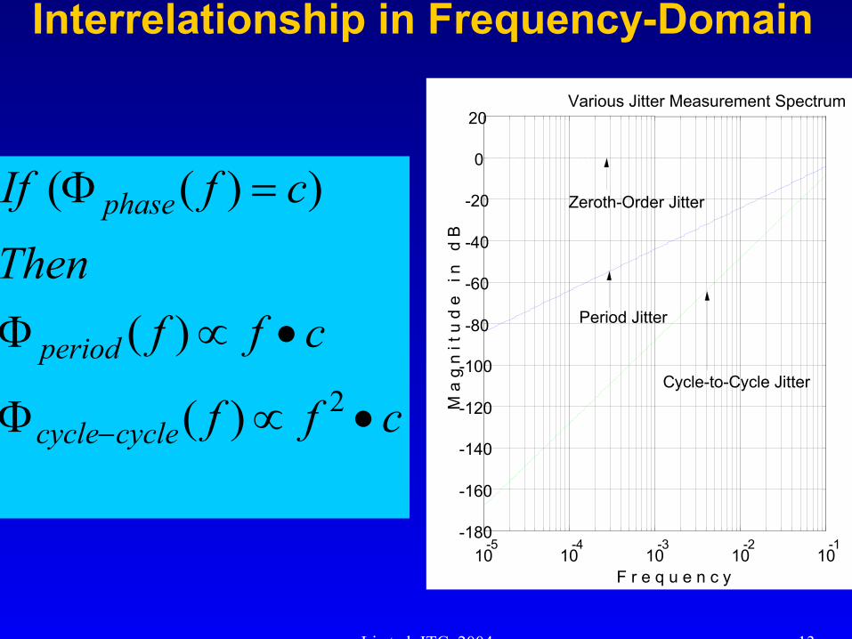
Interrelationship in Frequency-Domain
M a
g n
i t u
d e
i n
d
B
10-5
10-4
10-3
10-2
10-1
-180
-160
-140
-120
-100
-80
-60
-40
-20
0
20Various Jitter Measurement Spectrum
F r e q u e n c y
M a
g n
i t u
d e
i n
d
B
Zeroth-Order Jitter
Period Jitter
Cycle-to-Cycle Jitter
)(
)(
))((
2 cff
cffThen
cfIf
cyclecycle
period
phase
•∝Φ
•∝Φ
=Φ
−

Li et al, ITC, 2004 14
Phase Jitter Measurement and Reference Clock Used
• Calculating phase jitter against a warped clock (or recovered clock ) reduces the amount of phase jitter calculated
• The amount of warping depends on the recovered clock’s transfer function of the receiver
0
Data phase
Ref clock phase
Diff
Time
Phas
e

Li et al, ITC, 2004 15
Eye Closure/Total Jitter Modeling• Given a clock and data signal
• Eye closure is the difference in the phase between the clock and the data given by
• Eye closure direct depends on the jitter transfer function of the receiver
|)()(|)( tPtPtP dataclk −=∆
)]([)( 0 tPtVtV ClkClkClkClk += ω
)]([)( 0 tPtVtV DataDataDataData += ω
)(tP∆

Li et al, ITC, 2004 16
III. Jitter Transfer Functions

Li et al, ITC, 2004 17
• An output signal y(t) equals to the input signal convolves with the impulse response h(t)
• Phase jitter is modeled as continuous signal
LTI System in Time-Domain
∑ =
∫∞
∞−
−= τττ dthxty )()()(

Li et al, ITC, 2004 18
LTI System in S-Domain
• S-domain functions is obtained via Laplace transformation
• Complex frequency s can be related to the realfrequency ω through s = jω, as done in the models
Y(s) = X(s)H(s)
y(t) = Laplace-1 (Y(s))

Li et al, ITC, 2004 19
LTI System Summary
τττ dthxtxthty ∫∞
∞−−== )()()(*)()(
∫∞
∞−
−= )()( dtethsH st
)()()( sXsHsY =
L T I S y s t e m T i m e - d o m a i n : h ( t ) S - d o m a i n : H ( s )
x ( t ) y ( t )
X ( s ) Y ( s )
Li et al, ITC, 2004 20
IV. System Models

Li et al, ITC, 2004 21
Data Recovery Circuits (DRC)• Receiver Data Recovery is the essence of the
system
• Traditional Serial Communication uses a PLL based Data Recovery
• PCI Express allows a less expensive digital based Data Recovery Circuit
Using phase interpolator (PI), oversampled design or digital controlled delay lineMajority implemented DRCs are PIs

Li et al, ITC, 2004 22
PLL Based DRC• The system reference clock is not used when
recovering the data
• The Rx PLL needs to track the transmitter’s jitter output
Eye-closure/total jitter system model
Receiver inChip #2
u1x1
f (x1...xn)
PLLx25
Q
QSET
CL R
D
Transmitte rChip #1 - |Eye Closure |
W1
Y
ReferenceClock #1
X
u1x1
f (x1 ...xn )
DRC PLL
Data

Li et al, ITC, 2004 23
Digital PI Based DRC• Both Tx and Rx use the reference clock• Phase relationship between ref clock and data
path mattersEye-closure/total jitter system model
Receiver inChip #2
u1x1
f(x1...xn)
PLLx25 Q
QSET
CLR
D
u1
x2
x1f(x1...xn)
Phase Alignment
TransmitterChip #1
u1x1
f(x1...xn)
PLLx25
-|Eye Closure|
X
W_3
W_1
W_2
Y
Reference Clock

Li et al, ITC, 2004 24
Phase/Jitter Transfer Function For A PLL
• The input signal to a PLL is
where Pin(t) is the input phase signal and is the state variable of the PLL
• The output from a PLL is
where Pout(t) is the output phase.• The PLL has a phase transfer response h(t)/H(s), they
satisfy
( ))(sin)( tPtAtV inininin += ω
( ))(sin)( tPtAtV outoutoutout += ω
)(*)()( tPthtP inout = )()()( sPsHsP inout =
Li et al, ITC, 2004 25
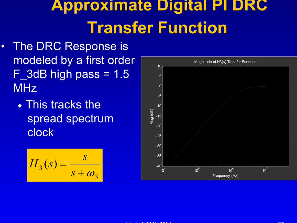
Approximate Digital PI DRC Transfer Function
• The DRC Response is modeled by a first order F_3dB high pass = 1.5 MHz
This tracks the spread spectrum clock
33 )(
ω+=sssH
104 105 106 107-40
-35
-30
-25
-20
-15
-10
-5
0
5
10Magnitude of H3(s) Transfer Function
Frequency (Hz)
Mag
(dB
)

Li et al, ITC, 2004 26
Model For A PLL Transfer Function• Can be approximated by
a 2nd order transfer functions for Rx and Tx
• Some PLLs are 3rd order or higher, additional poles at higher frequency do not contribute significantly to the eye closure
22
2
22
)(1nn
nn
sss
sHωζω
ωζω++
+=
1)21(21 2223 ++++= ζζωω ndB

Li et al, ITC, 2004 27
System Transfer Function Models
PLL Based DRC ModelPLL Based DRC Model
u1x1
f(x1...xn)
Rx PLL
-
W_1(s)
W_2(s)
Y(s)
u1x1
f(x1...xn)
Clock Reference
H_1(s)
u1x1
f(x1...xn)
TX PLL
X(s)
H_2(s) ( ))(1)()( 21 sHsHsH t −=
-
W_1(s)
W_2(s)
H_1(s)
H_2(s)
u1x1
f(x1...xn)
TX PLL
u1x1
f(x1...xn)
Rx PLL
W_3(s)u1x1
f(x1...xn)
Phase Alignment
H_3(S)
u1x1
f(x1...xn)
Clock Reference
X(s)Y(s)
Digital PI DRC ModelDigital PI DRC Model
)())()(()( 321 sHsHsHsHt −=

Li et al, ITC, 2004 28
Delay Model• Delay transfer function models into the system
The phase delay is given by (L1 + L2) – L3This is modeled by exp(-s * t_delay)
Receiver inChip #2
u1x1
f(x1...xn)
PLLx25
Q
QSET
CLR
D
u1
x2
x1f(x1...xn)
Phase Alignment
TransmitterChip #1
u1x1
f(x1...xn)
PLLx25
y_1
y_2w_4
L.1
L.2L.3
ReferenceClock

Li et al, ITC, 2004 29
Delay Transfer Function• Example with 100 ns
Delay• The transfer function has
nulls at the delay period• It has 6dB of gain at ½
intervals of the delay period
Doubles the effective jitter 100 102 104 106 108 1010
-120
-100
-80
-60
-40
-20
0
20
)]_*exp(1[ delaytsXY −=-X
u1x1
xy
Delay Y

Li et al, ITC, 2004 30
PLL Based Transfer Function• PLL Based DRC
does not have delay dependencies
• PLL locks to the data rate and wants a high Rx PLL response for best performance
u1x1
f(x1...xn)
Rx PLL
-
W_1(s)
W_2(s)
Y(s)
u1x1
f(x1...xn)
Clock Reference
H_1(s)
u1x1
f(x1...xn)
TX PLL
X(s)
H_2(s) ( ))(1)()( 21 sHsHsH t −=

Li et al, ITC, 2004 31
Digital PI Based Transfer Function• The difference
function includes an arbitrary phase delay not to exceed 30 ns
The delay “un-correlates” the clock/data and closes the eye
• This can be estimated with 2X multiplier of H1(s)-H2(s)
104 105 106 107-40
-35
-30
-25
-20
-15
-10
-5
0
5
10Transfer Functions Mag
Frequency (Hz)
Mag (dB)
F1: 7.0e+006 F2: 2.2e+007
H1H2H1(delayed 30ns) - H22* (H1-H2)H3
)()]()([2)( 321 sHsHsHsHt −=

Li et al, ITC, 2004 32
V. Applications of System Models

Li et al, ITC, 2004 33
Reference Clock Jitter Induced Eye-Closure Estimation
• Quantify system-level interdependencies Reference ClocksPLL parameters
• Calculate eye closure from the reference clock (most complex transfer function)
Using previously defined models

Li et al, ITC, 2004 34
PLL and Digital PI Parameter Ranges
1. The BW of the Tx and RX PLLs is 1.5 MHz to 22 MHz, 3dB peaking maximum
2. The BW of the DRC (PI) should be at least 1.5 MHz

Li et al, ITC, 2004 35
Models Applied to Measured Data: One Method
• X(s)The input spectrum can be measured by measuring a clock and applying the jitter definitions to get the phase jitterThe phase jitter signal is then transformed into the phase jitter spectrum, X(s)
• H(s)The models presented here give Ht(s), the bounding function, including the delay
• Y(s)Y(s) =X(s)H(s)

Li et al, ITC, 2004 36
Eye-Closure at The RX Sample Flop-One Method
• The inverse Laplace transform of Y(s) gives the eye closure in the time domain, y(t)

Li et al, ITC, 2004 37
Jitter “Peaking” and Broadening
A B
• Difference function dominated by Tx, Rx and Phase InterpolatorPLL bandwidth differencePLL peaking
• Reference clock noise spectrum as seen at Tx and Rx• Any noise under the difference function can cause phase jitter
• 3 Danger Areas (7-22 MHz shown) Between “A” and “B” ref clock jitter gets multiplied
Left of “A” rolls offRight of “B” rolls off
• Changing Tx, Rx below 7 MHz increases width of danger areas
Width and Amplitude Impact varies with clock spectrum

Li et al, ITC, 2004 38
VI. Summary and Conclusion
• A generic S-domain jitter transfer functions forPCIe were established
• A quantitative mathematical relationship between phase, period, and cycle-to-cycle jitter is developed
• Reference clock jitter transfer function is a ~(3th high-2th order low) band-pass
• The jitter state variable is Phase Jitter, and cycle-to-cycle is not the right merit for PCIe clock jitter
• Tx jitter transfer function is a 1st order high-passwith a 3dB frequency of 1.5 MHz
• The method developed here can also be appliedto new and relevant communication architectures (i.e., FB DIMM, SATAII etc. )