jawaharlal nehru engineering college - jnec.orgjnec.org/lab-manuals/ect/se/part-i/communication...
TRANSCRIPT

Jawaharlal Nehru Engineering College
Laboratory Manual
COMMUNICATION ENGINEERING
For
Second Year Students
Lab manual made by
PROF. S.A. ANNANDATE PROF. P. B. MURMUDE
PROF. P.B.YADAV
Author JNEC, Aurangabad.

MGM’S
Jawaharlal Nehru Engineering College
N-6, CIDCO, Aurangabad
Department of Electronics &Telecommunication
Vision of the Department:
To develop GREAT technocrats and to establish centre of excellence in the field of Electronics and
Telecommunications.
Global technocrats with human values
Research and lifelong learning attitude,
Excellent ability to tackle challenges
Awareness of the needs of society
Technical expertise
Mission of the Department:
1. To provide good technical education and enhance technical competency by providing good
infrastructure, resources, effective teaching learning process and competent, caring and
committed faculty.
2. To provide various platforms to students for cultivating professional attitude and ethical values.
3. Creating a strong foundation among students which will enable them to pursue their career
choice.

Jawaharlal Nehru Engineering College
Technical Document
This technical document is a series of Laboratory manuals of Electronics &
Telecommunication and is a certified document of Jawaharlal Nehru Engineering
College. The care has been taken to make the document error free but still if any error is
found kindly bring it to the notice of subject teacher and HOD.
Recommended by,
HOD
Approved by,
Principal

FOREWORD
It is my great pleasure to present this laboratory manual for second year engineering
students for the subject of communication engineering keeping in view the vast coverage
required for visualization of concepts of communication engineering.
As a student, many of you may be wondering with some of the questions in your mind
regarding the subject and exactly what has been tried is to answer through this manual.
Faculty members are also advised that covering these aspects in initial stage itself will
greatly relieve them in future as much of the load will be taken care by the enthusiastic
energies of the students once they are conceptually clear.
HOD

LABORATORY MANUAL CONTENTS
This manual is intended for the second year students of ECT/IE branches in the subject of
Communication Engineering. This manual typically contains practical/Lab Sessions
related to communication engineering, covering various aspects, related to the subject to
enhance understanding.
Students are advised to thoroughly go through this manual rather than only topics
mentioned in the syllabus, as practical aspects are the key to understanding and
conceptual visualization of theoretical aspects covered in the books.
Good Luck for your Enjoyable Laboratory Sessions.

SUBJECT INDEX
1. DO’s and DON’Ts in Laboratory.
2. Lab exercise
1. Study of RF Signal Generator.
2. Modulation index calculation by AM wave and
Trapezoidal pattern.
3. Pre-emphasis and De-emphasis.
4. Pulse width modulation.
5. Pulse position modulation.
6. Sampling and reconstruction.
7. AM Modulation & Demodulation
8. Pulse code modulation.
9. Study of Time Division Multiplexing.
3. Quiz on the subject.
4. Conduction Viva-Voce Examination.
5. Evaluation and Marking Systems.
DO’s and DON’Ts in Laboratory:
1. Do not handle any equipment before reading the instructions/Instruction manuals.
2. Read carefully the power ratings of the equipment before it is switched on whether
ratings 230 V/50Hz or 115V/60 Hz. For Indian equipments, the power ratings are
normally 230V/50Hz. If you have equipment with 115/60 Hz ratings, do not insert
power plug, as our normal supply is 230V/50 Hz, which will damage the equipment.
3. Observe type of sockets of equipment power to avoid mechanical damage.
4. Do not forcefully place connectors to avoid the damage.
5. Strictly observe the instructions given by the teacher/Lab Instructor.
Instruction for Laboratory Teachers:
1. Submission related to whatever lab work has been completed should be done during
the next lab session.
2. The promptness of submission should be encouraged by way of marking and
evaluation patterns that will benefit the sincere students.

Experiment No.1
Aim: To study RF signal generator.
Apparatus: Oscilloscope, RF signal generator, function generator, probes, etc.
Theory: RADIO-FREQUENCY (RF) SIGNAL GENERATORS
In addition to the necessary power supply, a typical RF signal generator contains
three other main sections: an OSCILLATOR CIRCUIT, a MODULATOR, and an
OUTPUT CONTROL CIRCUIT. The modulator modulates the RF signal of the
oscillator. In addition, most RF generators are provided with connections through which
an external source of modulation of any desired waveform can be applied to the
generated signal. Metal shielding surrounds the unit to prevent signals from the oscillator
from affecting the circuit under test.
A block diagram of a representative RF signal generator is shown in figure. The
function of the oscillator stage is to produce a signal that can be accurately set in
frequency at any point within the range of the generator. The type of oscillator circuit
used depends on the range of frequencies for which the generator is designed. In lower
frequency RF signal generators, the oscillating circuit consists of one of a group of coils
combined with a variable capacitor. One of the coils is selected by the position of a range
selector switch that connects the coil to a capacitor to provide an inductance-capacitance
circuit. The inductive-capacitance circuit then has the correct range of resonant
frequencies.
In amplitude modulation, the amplitude of carrier is changed in accordance with
Instantaneous value of modulating signal.The function of the modulator is to produce an
audio (or video) modulating signal that can be superimposed on the RF signal produced
by the oscillator. The modulating signal may be provided by an audio oscillator within
the generator. This is termed INTERNAL MODULATION. It may also be derived from
an external source. This is termed EXTERNAL MODULATION. In some signal
generators, either of these two methods of modulation can be employed. In addition, a
means of disabling the modulator section is available so that the pure, un-modulated
signal from the oscillator can be used when desired.

Fig: RF signal generator block diagram Waveform:

Procedure:
1. Connect the probe at output terminal of RF generator and another to the
oscilloscope.
2. Observe the waveforms for different RF frequency range (KHz-MHz).
3. Check the different waveforms on oscilloscope.
Conclusion:
We have observed AM waveform for different modulation indices. RF signal generator
internally combines message signal & carrier signal & produces modulated waveform.

Experiment No.2
Aim: To calculate modulation index of AM wave by using AM wave and
Trapezoidal pattern.
Apparatus: AM modulator kit, oscilloscope, AF function generator, probes, wires etc.
Theory:
Modulation means varying amplitude, frequency, phase of a higher frequency continuous
wave carrier signal with information waveform. In amplitude modulation,
the amplitude means signal strength of the carrier wave is varied in proportion to the
waveform being transmitted.
%𝒎 =𝑳𝒎𝒂𝒙−𝑳𝒎𝒊𝒏
𝑳𝒎𝒂𝒙+𝑳𝒎𝒊𝒏× 𝟏𝟎𝟎
Where, L max , L min are lengths of trapezoidal Pattern.
Procedure:
1. Give supply to the kit of AM/ FM generator.
2. Using function generator give information Signal to AM/ FM generator
External Nob.
3. Measure the information wave & draw the waveform.
4. Connect the information signal to oscilloscope Channel 2.
5. Connect AM/ FM generator output to Channel 1of oscilloscope
6. Calculate E max (p-p) &E min (p-p) for 3 set of different readings.
5. Press the X-Y Nob.

Observation:
%𝒎 =𝑳𝒎𝒂𝒙 − 𝑳𝒎𝒊𝒏
𝑳𝒎𝒂𝒙 + 𝑳𝒎𝒊𝒏× 𝟏𝟎𝟎
Sr. No. LMax (p-p) LMin (p-p) % M
Conclusion:
It has been observed that as modulating signal voltage increases, modulation index
also increases i.e. Em α m.

Experiment No.3
Aim: I) To observe the effects of pre-emphasis on given input signal.
II) To observe the effects of De-emphasis on given input signal.
Apparatus: Resistors (10 KΩ, 7.5 KΩ, 6.8 KΩ), Capacitors (10 nF, 0.1 µF), CRO,
Function Generator
Theory:
The noise has an effect on the higher modulating frequencies than on the lower
ones. Thus, if the higher frequencies were artificially boosted at the transmitter and
correspondingly cut at the receiver, an improvement in noise immunity could be
expected, thereby increasing the SNR ratio. This boosting of the higher modulating
frequencies at the transmitter is known as pre-emphasis and the compensation at the
receiver is called de-emphasis.
Circuit Diagrams:
For Pre-emphasis:
Fig.1. Pre-emphasis circuit

For De-emphasis:
Fig.2. De-emphasis circuit
Procedure: 1. Connect the circuit as per circuit diagram as shown in Fig.1.
2. Apply the sinusoidal signal of amplitude 20mV as input signal to pre emphasis
circuit.
3. Then by increasing the input signal frequency from 500Hz to 20 KHz, observe
the output voltage (vo) and calculate gain (20 log ( vo /vi).
4. Plot the graph between gain Vs frequency.
5. Repeat above steps 2 to 4 for de-emphasis circuit (shown in Fig.2). by applying
the sinusoidal signal of 5V as input signal
Observation:
Table1: Pre-emphasis Vi = 20mV
Frequency(KHz) Vo(mV) Gain in dB(20 log Vo/Vi)

Table2: De-emphasis
Vi = 5v
Frequency(KHz) Vo(Volts) Gain in dB(20 log Vo/Vi)
Graphs:
Conclusion: -
Hence we have studied pre-emphasis and de-emphasis.
Experiment No.4
Aim: To study pulse width modulation
Apparatus: PWM kit, oscilloscope, function generator, probes.
Theory:
Pulse width Modulation (PWM) is also known as Pulse duration Modulation
(PDM). Three variations of PWM are possible. In One variation, the leading edge of the
pulse is held constant and change in the pulse width with signal is measured with
respect to the leading edge. In other Variable, the tail edge is held in constant and with
respect to it, the pulse width is measured in the third variation, the centre of the pulse is
held constant and pulse width changes on either side of the centre of the pulse. The
PWM has the disadvantage when compared to ‘PDM’ that its pulses are of varying
width and therefore of varying power content, this means the transmitter must be
powerful enough to handle the max width pulses.
The PWM is actually a square wave modulated. This modulation infects on the
frequency (clock cycle) and the duty cycle of the signal. Both of those parameters will
be explained in details later but keep in mind that a PWM signal is characterized from
the duty clock and the duty cycle. The amplitude of the signal remains stable during
time (except of course from the rising and falling ramps). The clock cycle is measured
in Hz and the duty cycle is measured in hundred percent.
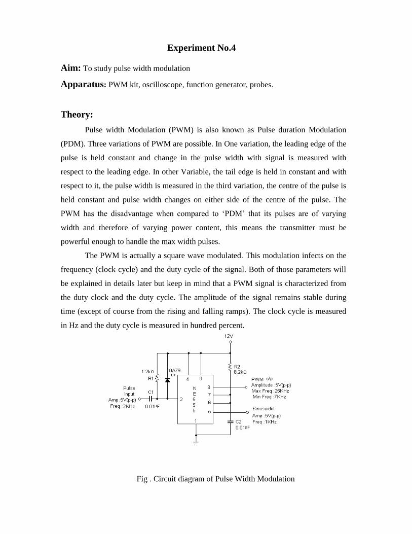
Fig . Circuit diagram of Pulse Width Modulation

Source signal
PWM signal
Procedure:
1. Connect the probes to CRO and PWM kit.
2. Check its output at pin no. 3.
3. Take the reading for different voltages.
Observation:
Sr. No Modulating Voltage (tp in units) ∆𝒕𝒑
Conclusion: Hence we have studied that for change in voltage there will be change width. For
maximum voltage output is having large width & at minimum voltage pulse having
very small width.
Experiment No.5
Aim: To study pulse position modulation
Apparatus: PPM kit, function generator, probes.
Theory:
In Pulse Position Modulation, both the pulse amplitude and pulse duration are
held constant but the position of the pulse is varied in proportional to the sampled
values of the message signal. Pulse time modulation is a class of signaling techniques
that encodes the sample values of an analog signal on to the time axis of a digital signal
and it is analogous to angle modulation techniques. The two main types of PTM are
PWM and PPM. In PPM the analog sample value determines the position of a narrow
pulse relative to the clocking time. In PPM rise time of pulse decides the channel
bandwidth. It has low noise interference.
Pulse-position modulation (PPM) is a signal modulation used for both analog
and digital signal transmissions. This method is widely used for optical communication
systems such as optic fiber and IR remote controls, where efficiency is required and
little or no external interference occurs.
In PPM, data are transmitted with short pulses. All pulses have both the same
width and amplitude. The parameter that changes is the delay between each pulse.

Fig . Circuit diagram of Pulse Position Modulation

Procedure:
1. Connect the probes to CRO and PPM kit.
2. Check its output at pin no. 3.
3. Take the reading for different voltages.
Observation:
Sr. No Modulating Voltage (tp in units) ∆𝒕𝒑
Conclusion:
Hence we have studied that for change in voltage there will be change position. In
positive cycles pulses are dense it becomes rare in negative cycle.

Experiment No.6
Aim: To study sampling of a signal and its re-construction.
Apparatus: Analog Signal Sampling & Reconstruction Kit, 20 MHz Dual Trace
Oscilloscope, Patch Chords
Theory:
SAMPLING FREQUENCY: The 6.4 MHz Crystal oscillator generates the 6.4 MHz
clock. The decade counter divides the frequency by 10 and the ripple counter generate
the basic sampling frequencies - 320 KHz to 20 KHz and the other control
frequencies. The basic sampling frequencies is given to a multiplexer For each "Press"
on the frequency select switch, the output of the state counter increases by one and it
counts from 000 to 100. As the state counter counts from 000 to 100, the
corresponding input of the multiplexer is switched to the output. As soon as the count
reaches 101, the output of the 3 to 8 decoder resets the state counter and the whole
cycle repeats. Also LED connected to the output of the decoder is switch ON, which
indicates the sampling frequency selected. Refer the truth table for better
understanding.
Procedure:
1. Connect power supply in proper polarity to the kit & switch on.
2. Connect the l KHz, 5V pp Sine wave signal, generated onboard, to the
ANALOG INPUT, by means of the patch-cords provided.
3. Connect the sampling frequency signal in the internal mode, by means of the
shorting pin provided.
4. Using switch SW1 select 50% duty cycle as shown in the table.
5. Connect the SAMPLE OUTPUT to the input of the 2nd Order Low Pass Filter.
6. Using frequency selector switch, select desired sampling frequency. The selected
sampling frequency is indicated by the glowing LED.
7.Take observation as mentioned below for various sampling frequency: 32 KHz,

16KHz, 8KHz, 4KHz , 2KHz.
Conclusion:
From the above observations we conclude that as the Sampling Frequency is increased,
the reconstructed output is less distorted and almost original signal is reconstructed. For
a sampling frequency of 2KHz, only 2 samples of the 1KHz signal are taken; whereas
that for a sampling frequency of 8KHz, 8 samples of 1KHz signal are taken.
Hence, as the number of samples taken of the signal increases, the distortion of the

Re-constructed signal decreases.
As per the Nyquist Criterion at least two samples are required for the
reconstruction if the signal. If the Nyquist Criterion is not satisfied, or if the signal
is not band limited, then spectral overlap, called "aliasing" occurs, causing higher
frequencies to show up at lower frequencies in the recovered message, and
specially in voice transmission intelligibility is seriously degraded Thus,
universally for the voice band (300Hz to 3300Hz), the sampling frequency used is
8KHz, which satisfies the Nyquist Criterion.

Experiment No. 7
Aim: 1. To generate amplitude modulated wave and determine the % modulation.
2. To Demodulate the modulated wave using envelope detector.
Apparatus: Transistor (BC 107), Diode (0A79), Resistors (1KΩ, 2KΩ, 6.8KΩ, 10KΩ),
Capacitor (0.01µF), Inductor (130mH), Function Generator, Regulated Power Supply
Theory:
Amplitude Modulation is defined as a process in which the amplitude of the
carrier wave c(t) is varied linearly with the instantaneous amplitude of the message
signal m(t).The standard form of an amplitude modulated (AM) wave is defined by
st Ac1 K amtcos2f c t
Where, Ka is a constant called the amplitude sensitivity of the modulator.
The demodulation circuit is used to recover the message signal from the incoming AM
wave at the receiver. An envelope detector is a simple and yet highly effective device
that is well suited for the demodulation of AM wave, for which the percentage
modulation is less than 100%.Ideally, an envelope detector produces an output signal
that follows the envelop of the input signal wave form exactly; hence, the name. Some
version of this circuit is used in almost all commercial AM radio receivers.
The Modulation Index is defined as,
m =Emax − Emin
Emax + Emin
Where, Emax and Emin are the maximum and minimum amplitudes of the modulated
wave.

Circuit Diagrams:
For modulation:
Fig. AM modulator
For demodulation:
Fig. AM demodulator
Procedure: 1. The circuit is connected as per the circuit diagram shown in Fig.1. 2. Switch on + 12 volts VCC supply.
3. Apply sinusoidal signal of 1 KHz frequency and amplitude 2 Vp-p as modulating

signal, and carrier signal of frequency 11 KHz and amplitude 15 Vp-p. 4. Now slowly increase the amplitude of the modulating signal up to 7V and note
down values of Emax and Emin.
5. Calculate modulation index using equation
6. Repeat step 5 by varying frequency of the modulating signal.
7. Plot the graphs: Modulation index vs Amplitude & Frequency
8. Find the value of R, fm=1
2πRC.
Where, C=0.001uF.
9. Connect the circuit diagram as shown in Fig.2.
10. Feed the AM wave to the demodulator circuit and observe the
output.
11. Note down frequency and amplitude of the demodulated output
waveform.
12. Draw the demodulated wave form m=1.
Observation:
Table 1: fm= 1KHz, fc=11KHz, Ac=15 V p-p.
Sr. No. Vm(Volts) Emax(volts) Emin (Volts) m %m (m x100)
Table 2: Am= 4 Vp-p fc =11KHz, Ac=15 V p-p.
Sr. No. fm(KHz) Emax(volts) Emin(Volts) m %m (m x100)
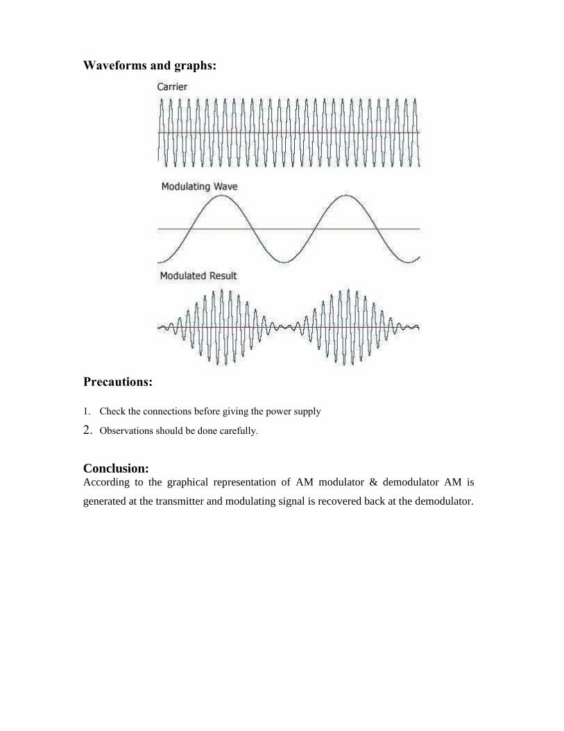
Waveforms and graphs:
Precautions:
1. Check the connections before giving the power supply
2. Observations should be done carefully.
Conclusion: According to the graphical representation of AM modulator & demodulator AM is
generated at the transmitter and modulating signal is recovered back at the demodulator.

Experiment No.8
Aim: To study pulse code modulation
Apparatus: PCM kit, oscilloscope, function generator, probes.
Theory:
Pulse Code Modulation is also known as a digital pulse modulation technique.
The pulse modulation (PCM) is quite complex compared to the analog pulse
modulation techniques(i.e. PAM, PWM, PPM) in these sense that the message signal
is subjected to a great number of operations. Fig. shows the basic elements of a PCM
system. It consists of three main parts i.e. transmitter, transmission path and receiver.
The essential operations in the transmitter of a PCM system are sampling, quantizing
and encoding as shown in fig.1.Sampling is operation in which an analog (i.e.
continuous -time) signal is sampled according to the sampling theorem resulting in a
discrete-time signal. The quantizing and encoding operations are usually performed in
the same circuit which is known as an analog-to-digital converter (ADC).
Also the essential operations in the receiver are regeneration of impaired signals,
decoding and demodulation of the train of quantized samples. These operations are
usually performed in the same circuit which is known as digital-to-analog converter
(DAC).
To transmit digitally an analogue signal such as speech or music, the analogue
signal must be regularly sampled. The stream of samples is then converted into digital
form, i.e. digitised, by an analogue-to-digital converter (ADC). This process is known
as pulse code modulation. On reception of the digital signal, digital-to-analogue
conversion takes place. It was explained in topic that an ADC is an integrated circuit
(IC) that has one input pin, which accepts an analogue voltage of any value, and n
output pins, which produce a corresponding n-bit binary number. The diagram below
shows how this IC can be used to transmit an analogue signal in digital form.

The sampling gate circuit repeatedly samples and stores for a brief period, the
value of the analogue voltage at some moment in time (remember that the analogue
signal varies continuously with time). The rate at which such samples are taken is
governed by the frequency of the sampling clock.
The ADC converts each sample of the analogue information into a code of n
bits. These n-bit codes are transmitted in parallel along n wires, one sample after
another, to a matching n-bit digital-to-analogue converter (DAC). This produces a
stepped analogue voltage from the incoming codes.
The output is often referred to as a staircase approximation to the original
analogue signal. The reconstitution filter is essentially a filter circuit that smoothes out
the quantisation steps from the DAC. It operates in such a way that it appears to change
the staircase waveform into a smooth curve.

Conclusion:
Hence we have studied Pulse Code Modulation.

Experiment No 9:
Aim: To study Time division Multiplexing
Theory:
Why multiplexing?
It is best on several observations. First one is it has been found that most individual data
communication devices typically require modest data rates. For example, when you are
sending the requirement is only 4 Kbps and obviously 4 KHz that is the bandwidth of course
whenever you convert it in digital form then it comes to 64 Kbps then of course that one is
also not very weak. Similarly the average data rate required is also not very high.
Fig: Block diagram of TDM
Time-division multiplexing is used primarily for digital signals, but may be applied
in analog multiplexing in which two or more signals or bit streams are transferred appearing
simultaneously as sub-channels in one communication channel, but are physically taking
turns on the channel. The time domain is divided into several recurrent time slots of fixed
length, one for each sub-channel. A sample byte or data block of sub-channel 1 is
transmitted during time slot 1, sub-channel 2 during time slot 2, etc. One
TDM frame consists of one time slot per sub-channel plus a synchronization channel and
sometimes error correction channel before the synchronization. After the last sub-channel,
error correction, and synchronization, the cycle starts all over again with a new frame,

starting with the second sample, byte or data block from sub-channel 1, etc.
Fig: Waveforms of TDM
Conclusion:
Time Division Multiplexing allows equal time period for each channel.

4. Quiz on the subject: 1) What is standard IF value for AM receiver & FM receiver?
2) In a receiver which stage rectifies the IF signal?
3) From which component the three point tracking is achieved?
4) Define double spotting, image frequency, sensitivity, selectivity & fidelity.
5) Define carrier signal, modulating signal & modulated signal.
6) How many side bands exist in AM&FM?
7) Define frequency spectrum in AM.
8) What is the use of Bessel’s function?
9) What is the disadvantage of FM over AM?
10) What are the different types of detectors in AM & FM?
11)What are the different forms of AM?
12) What is AGC? What are its types? State use of it?
13) What is band spreading?
15) What is ganged tuning?
16) Which stage of AM & FM receiver determines the gain?
17) Define bandwidth. State the B.W. of AM & FM signal.
18) Define balanced modulator.
19) What are the o/p components of BM.?
20) What are the different types of BM?
21) ) What is SSB? What are its types?
22) State the different AM & FM generation methods?

5. Conduction of Viva-Voce Examinations:
Teacher should conduct oral exams of the students with full preparation. Normally, the
objective questions with guess are to be avoided. To make it meaningful, the questions
should be such that depth of the students in the subject is tested. Oral examinations are to
be conducted in co-cordial environment amongst the teachers taking the examination.
Teachers taking such examinations should not have ill thoughts about each other and
courtesies should be offered to each other in case of difference of opinion, which should
be critically suppressed in front of the students.
6. Evaluation and marking system:
Basic honesty in the evaluation and marking system is absolutely essential and in the
process, impartial nature of the evaluator is required in the examination system. It is a
wrong approach or concept to award the students by way of easy marking to get cheap
popularity among the students, which they do not deserve. It is a primary responsibility of
the teacher that right students who are really putting up lot of hard work with right kind
of intelligence are correctly awarded.
The marking patterns should be justifiable to the students without any ambiguity and
teacher should see that students are faced with just circumstances.