ithaca intersystems series ii z-80 processor manual manuals/intersystems/ithaca...intersystems...
TRANSCRIPT

InterSystems Series II Z-80 Processor
fot the 5-100 Bus
User's Manual
Copyright. 79 byIthaca InterSystems,
hiterSystems Publication 2000'~L


Ser5.E~~"3 II
InterSystems Series II eta the first integrated oomputer systemdesigned entirely to IEEE S·,,100 StandaJi'd:s. As such w it represents apOiiJerful and versatile family of COlU1.put.ers and aecessories you can apply tovirtual any computing task,
With Series II you have considerable flexibi in systemsbeoause the Series II architecture is modular and not tied to any partioulartype of computirlg. This modular and structur"al stability enables you toadapt y·ol.U~ system eas to YOUA~ computing needs.
As ,41th ;al1 InterSystems Series II Products 9 the Series II Z-80 has beendesigned to take full advantage of the extensions and enhancements of thenew IEEE 5-100 bus specification l and remain compatible with themajority of pre-standard 5-100 boards.
This oiNner! s manual haJJ to ac;quaj.nt you with your processor'and to serve as an aid in achieving its use. Section 1 intr~duce5
the Ser"1es II and prov1des some general inf(u'mation; Sectl.on 2desm~ibes the use of the board' in a system! hOoN' to use the memm'y managementunit, vectored inter"x"upt controller' and othel~ board feature,'S, andprogrsllll'Iling examples SeeUon 3 is a step~by"·step gUide to of theboa.rd. rOle operatlon in your em~ and remaining seeU.onstechnical details, list, and d
Your Series II pJrocessox' has been fully tested and burned in a.t tbeInterSystew.s factory ~ and should W\lOd, the fi.rst. tim.e in your system. Ifyou have any problems with the unit in your system, give us a oall at (607)257·,,0190; our technical support personnel "rill be glad to assist you.

I: .. r·; I; 1'1 T hr d :i. -1:, :i. 01"'1 :I. ~ /. ... U0 :I. J t1 d II U .•• J
i1a':! :L ':;)}' :L '/UO
Th €~ f () 1. ]. D C,J i 1"1 :.:.{ m~:~ t t:! Y' :r. iIi :J. 1.,,1 :i. J:I. b f·., :i. 1-, COY' F' 0 Y' ;;1 t .. ~:' (.j i I"i t C) I: .. ,.:.1 i t. :I. C 1"\ ., ..
of the Z-80 II Manual.
LPF:UM ,.Jum:··,p Y' CJF·t:l. C,II"\:::
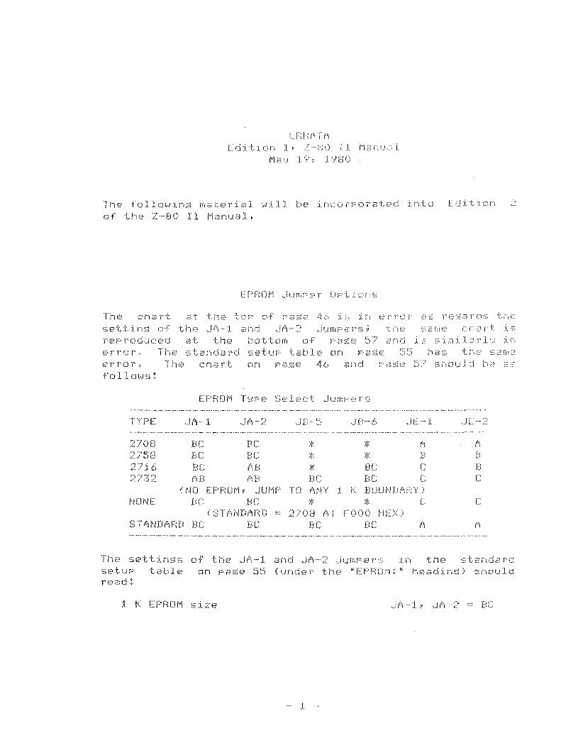
Th (,,' C h ~1 1" t cl t the t. D F' C) f F' iIi '.:j, ';:'.' j~ '!) :i.::: :i. n E·!":" roy' i:::::; r E·:' :;,:: .:::: Y' d·:::. t, j"·I":·.'
,,;E' t t. in'."; C)'I:' thf·.' .!f1·..·J ;;In d -..I('\ .... :? ,.iUIYJ:::" e r·,::. ~ t. i'''1C':'. .;::. ,:;: 11'1 ('.'.' c: h a r' t :i. ,,:.r!:.,' P rodu C t:·.' d cit t hf') hot to m ()·f F" a:':.~t~! ~:.;? a 1"\ ij :i. '::.:::.:i. Ii'i :i. J .;:,: Y' :I. '::;: :i.1"1error. The standard setup table on pa~e 55 has the S2me(;.) r T' () r • ThE') C h art 0 n p a '.'.{ (.) 46 i:' nd F" 2 ;:.,,; ."" ~:.;.::.. ~:; h C) 1,.1 .I. i:.) b c·:·, i:, .:::'fDll[)~J<:; ~
TYPE "lA·..·:!. JI::..... 1 ...11::..... )
2708 BC BC2758 BC BC2716 BC AB2J32 AB AB
( N() EY f;: () t1? .J l.J Mr:'NONE BC BC
(bTf)NDI'1nI! ""STANDARD BC BC
* * h)V * Y.)I' '.'i' BC C".f{C 1"C C":1 .."
TU MFi 1. i< BULJ N1.1 (') 1': y )
* >1:: C270H hf FOOO He\)
Be DC.:
(')
r:f:C
Th(0 ~:;~;)tt:i.n£{s
S;(0tUP tablE!r0)ad ~
ofth c J ('I .... J ii; n d J A.... ::~ ~j U H, :.::. ';;'.' 1" ·c:. :I. I"! the ~:. t. a n ij d 1" iJ
on paSe 55 (under the "[PROM:" hesdinS) Should
Jh··.. :I. Y ...1f'I·..·2 .... I:'C
1

(; C) rT, '.:' 1", c 1 00" 1.1 T' C'
"f h f'~ ?: -- E'; 0 1 I t1 U ~:'. 1"' d J,~; l"' Q -f c:~ 1~ r c: ('j t u d~; t h c!
most IntersYstoms' literature.
II lll"'U UO II
Th t:' Z ... 80 I I :i, ;::. d t·' <;:. i ~.{ I""! t:' d tom ;:,' t 0)) \.,) :i, t h <:i of rOI'"l t }':, d 1"'1 (.:.) :I. "/ ]. a.:::, :l. ,~:, ....f) I' ~:? () ..,. F' :i, I"! nIP c a r:.\ 1 (,~ • l h (::~ ? 0 -.. :.,' :I. 1"1 Li .I. F" C ;:i t,\ J (.:, i ,,,. I"! C) t. <:; 'v' .::~ :i. J .:::: \':.\ :I. (:)i n F' rod U Co' t ion (-l U i:! n t i. t i. t:' '::; .:::: t t hi':::. t, i. iii \;:\ !I ;::; n d :i. 1"1 IT! 0 ,,,. t c U ). f' C,' 1"1 tapplications the 16-pin DIP cable is used. The socketprovided on the /-80 II card is, however, a 20-pin socket,providin~ fa upward compatibility whel~ 20-Pln DIP cablesf.) ~:.~ com E:~ a '·1 a :i. 1 a r:J .I. (-." • T h c' :1. {:. .... r, :i, r', C i31·:.< 1. t." ~::. h 0 u J d b (',1) I) ';:. ~:~ ...-.; j, I-, t h ], ':;so ck t·) t F{ I Ci HT ju~:: t:i. f :i, e('\ "., ,",. t.h<:; -1:, i ~;; ~ h 0:1. cl 1 n ~:~ t, il t) h!::'U·..,b 0 C: .'::; rU"I i t h t h (,:) h"" J 00 c Cl nne c t D r F' 0 i 1"1 t :i. 1'"1 ::'.~ d () "II"! :' 1 () 0 I<. i. n,,~ ;:; t t j"j fl
COI1IP(JI"iE'nt E::i.d(:.' u-f-' th(-." t'iDdl"dl' tht:·) :!.()····r::i.n c:::;b.l.£, ,,;hol..-'].'.:) ~:!() :i.l'ltDt h (';' h (':., <3 C.1 (-"" Y' ':; 0 L' k (,,) t ~:; D t hat i t J:i 1""1 (:,\ ':;. U :." IA]. t. h t·j·j (':'.' r' 1 :J h t, :-:::i, C.) C~ 01:
t h (-:::' h t" i:; d (.:.: r' soc 1--:. (-.':' t 1 ;" ri d :I. (:'\ a 'v' (':,' .::; f u U Y' F' :i. n F' 0 ',; :i. t :i. 01"1 ',; e IYJ :.: t. ':! .:: tthe left side of the hCdder socket.
I I""i t hi::" C a -::; t)' Cl f t hi":" J 1"'1 t C') r ':;. '::; -::; t (." Hi ':; .f."' run t. F" ;:; r', (?:I." I.:- h (-.' l' J F' co::: ~J .I. ...:.,will be properlY 21i~ned if no tWIst is introduced into it,." .... t, hat i ~,;, :i. f th(·.o' r :i. ::,;~h t ':;:i. f.:lf.' u f' t h (.',' LIT Ii,' '::·oc k fl tun t hI:.:: f' Y' C) 1"1 t.F' ant·: 1 :i. :::' 0':1. t') c t r' i c a J 1 '::1 conn t:·) c t (.:.) cl tot. h f' r ]. ::-:~ h t ':;,:i. Cl c,~ u .r:' t h (,:' X,I J F:'~:;ocl--:. (,,) t on t h"," l-·· !JO I I c <,1. r'd " {\':::,]"' l:~~;.j;:; r d '::;. 0 t 1"'1 f.' rf Y' 0 n t r:' dl"i e.l. -:::. ~
con n t:.' c t t h (-.0' Ii IF:' C ii; b 1 F' s; 0 t h ,:;l t d;:; t i3 b j. t. z (,.) ]"' 0 :::10 C:.' ~::' t (1 t h (:,:r i ~2{ h t -::; i ;:.1 E' 0 F t h f'~ Ii I F' :;; 0 c k (,:: ton t h (.:.~ 7. .... U(1 J I ~ ..:.1 d t i:; bit :J. :::,; :;;) t:·::::toth (,,) n E\ >; t F':i. n t Cl t h (:: :I. 0: .1'.' t ~ 2; 1'"1 d ',I. CJ f D r th "

TABLE OF CONTENTS
1.0 Introduction and General InformatIon
1.1 Introducing the Series II 2-801.2 Service InformaUon
He otlanFactory ServlceContacting InterSystems
2.0 Series II 2-80 Architecture
23
·334
5
2.12.2
2.52.6
2.72.82.92.10
System Design OverviewAddress Management for La~ge Systems
Hemor'y Management SubroutinesInterrupt Handling with the Series II 2-80Z-80 Processor Interrupt Modes
Mode 0Hode 1Hade 2
Interrupt Controller ArchitectureInterrupt ControllerOperating Options
Fixed or Rotating PrioritiesCommon amI Individual VectoringPolledHaster Mas.!.;::Status RegisterInterrupt Service Register (ISH)Informs tion Transfers
Comma.nds to the Tnt ControllerUsing the Interrupt ControllerSeries II Bus InterfaceDirect Memory Acoess Operations
{)
7'1216181818191920
21222.222232}-I
2424283637
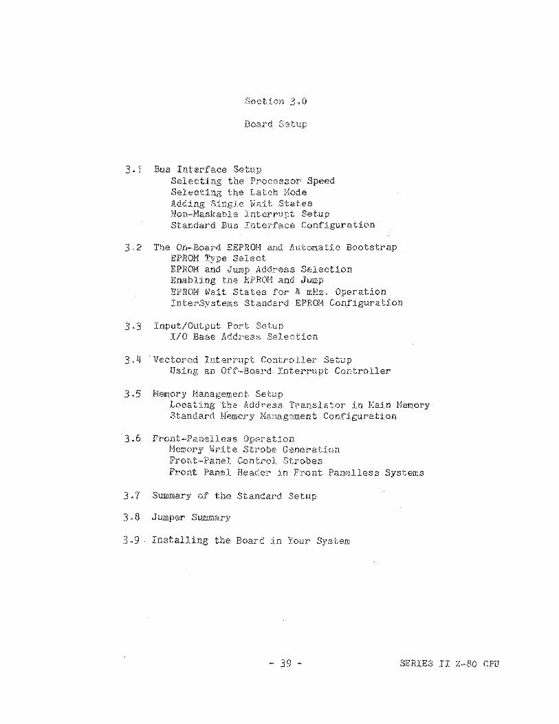
3.0 Board Setup·
3.1 Bus Interface ~etup
Selecting the Processor SpeedSelecting the Latch ModeAdding Single Wait StatesNon-Maskable Interrupt SetupThe On-Board EPROM and Automatic BootstrapEPROM Type SelectionEPHON and .Jtlmp Address SelectionEnabling the EPROM and ,JumpEPROM Walt States for )-1 Hhz OperationInterSystems Standard EPROM Configuration
39
)-1142424343454.5,;464747}~7
48
3.3 Input/Output Port SetupI/O Base lddress Selection
3.4 Vectored InterruptController Setup
Using an Off-Board Interrupt Controller3.5 Memory Management Setup
Locating the Address TranslatorStandard Memory Management Configuration
3.6 Front-Panelless OperationMemory Write Strobe GenerationFront-Panel Control StrobesThe Header in'Front Panelless Systems
3.7 Summary of the Standard Setup3.8 Jumper Summary3.9 Installing the Board
4.0 Technical Reference
4.1 S-100 NDEF Lines4.2 Testing Modes4.3 Board Timing Diagrams
5.0 Parts List and Placement
6.0 Revisions and Manual Applicability
7' .0 Schemati,c Diagram
Ithaca Intersystems Limited Warranty
4950
5051515253535354555760
61
626365
69
73
75
77
SecLlon 1
Introduction and General Information
'·.1 lritroducing the Series II 2-80
1.2 Service Ir~ormation
Receiving InspectionReplacement PartsFactory ServiceContacting InterSystems
1.1 Introducing the InterSystema Series II 80
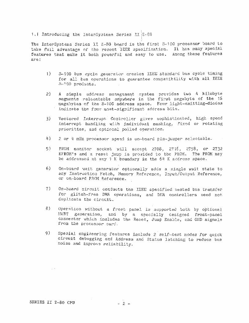
The InterSystems Series II Z-80 board is t~e first S-100 processor board totake full advantage of the recent ~EEE specification. It has many speoialfeatures that make it both powerful and easy to use. Among these featuresare:
1) 3-100 bus cyole generator creates IEEE standard bus cyole timingfor all bus operations to guarantee compatibility wl th all IEEES-·'OO products.
2) A slmple address management system provides two 4 kilobytesegments relocatable ariywhe!~e in the first megabyte of the 16megabytes of the 3-100 address space. Four light··emitting-diodesindicate the four most-significant address bits.
Vectored Interrupt Controller gives sophisticated!.i.l:1Itel~rupt handling 'ifJi th indiv:Ldual masking p fixedpriorities. and optional polled operation.
high speed.or rotating
4) 2 or 4 mHz processor speed is on-board pin-jumper selectable.
5) PHON monitor socket w.i11 accept 2708. 2716, 2758. or 2132EF'Rm1i s and a reset jump is pX'Cnrided to the PROM. The PROM maybe addressed at any 1 K boundary in the 64 K address space.
6) On-board wait generator optionally adds a single wait state toany Instruction Fetch. Memory Reference, Input/Output Reference,or oDo-board PROM Reference.
7) On-board circuit conducts the IEEE specified nested bus transferfOl~ glitch-f'l~ee DMA operations v and DHA controllers need notduplicate the oircuit.
8) Operation ltJithout a front panel is supported both by optionalH}lRT gener.ation~ and. by a specially designed front-panelconnector which inoludes the Reset~ Jump Enable~ and GND signalsfrom the processor card.
9) Special engineering features include 2 self-test modes for qUickcircuit debugging and Address and Status latching to reduce busnoise and ~nprove reliability.
SERIES II Z-80 CPU _. 2 _.
1.2 Service Informs tion
Receiving Inspection
Hhen your InterSystems 'Processor Nodule ar1'1yes ~ 1Dspect both the equipg!l~ni~
and the shipping carton immediately for evidence of damage during transit.If the shipping carton is damaged or ~'IIater-,stained, request the caJ~rier i is
agent" to be pr'esent lAlhen tb,e cal~ton is opened" If the carrier's agent isnot present when the oarton is opened, and the contents of the carton aredamaged 9 save the CiiH~ton and packing material for the agent! s inspection.Shipping dBlllages should be immedi.ately ed to the carrier, Do notattempt to servioe the board yourself as this will void the warranty.
We advise that in any case you shOUld save the shipping container for use inreturning the module tel" Inte14 Systems, should it become necessary to do.
Factory Service
Inte~'Systems provides 8. factory' repalr service fOl~ all of its products,Before returning the module to InterSystems , first obtain a ReturnAuthorization NU1l1bE~1~ from our Sales Dept,. This may be done by calling us,sending us a TWX, or by wri to us. After the return has beenauthorized, prooeed as follows:
1) Write a letter desoribing the problem as best you oan.
2) Del:3cribe your system to us ~ list boards by Hanu.fact1.lrer andname.
3) Include Xerox copies of the schematics of boards by manufacturersother than InterSystems.
4) Inolude the Return Authorization Number.
5) Pack the above informatiqn in a container suitable to the methodof shipment.
6) Ship prepaid to InterSystems.
Your module w:lll be repai).~ed as soon as poss.ibls after receipt and returnshipped to you prepaid.
SERIES II Z-80 CPU
Contacting InterSystems~
The following apply both for correspondence and service.
Ithaca InterSystems Inc.1650 Hanshaw Rd.P.O. Box 91Ithaca N.Y. U.S.A.
14850
In Europe:
TelephoneTWX
(601) 257-0190510 255..4346
Ithaca InterSystems (U.K.) Ltd.58 Crouch Hall RdLondon N8 8HG. U.K.
SERIES II Z-BO CPU
TelephoneTelex
.~ 4 ..
01-341,-2441299568
Section 2.0
Series II Z-80 Architecture
2.1 System Design Overvie'oN
2.2 Address Management for Large SystemsMemory Management Subroutines
2.3 Interrupt Handling with the Series II z~80
2.4 z-80 Processor Interrupt Modesr·1ode 0rejode 'j
Mocle 2
2.5 Interrupt Controller Architecture
2.6 Interrupt Controller Operating OptionsFixed or Rotating PrioritiesCommon and Indiv.idual VectoringPolled ModeHaster NaskStatus Regist.erInterrupt Service RegisterInformation. Transfers
2.7 Commands to the Interrupt Controller
2.8 Using the Interrupt ControllerVectored Interrupt Controller Handlers
2.9 Series II Bus Interface
2.10 Direct Hemory Access Operations
SERIES II Z-80 CPU
The Series II architecture supports a full range of system requirements~
from small" ded.icated applications to complex, lIiU.l ti·"·tasking systems, As amodUlar computing system, it. is a flexible base fl~om which to build asystem tailored to your computing needs and achieve;'
lI!f Outstanding p:r5.ce!perforroance for all size systems.
• High standards of re and serviceability through the useof proven technologies. close adherence to the IEEE S-100standard. and modular construction.
Expandability to meat your future needs.
2.1 System Design Over'vielJ'J
InterSystems Series II offers an :Lntegrated hardware and software systemdeveloped fOJ(' the IEEE S=,1 00 bus. At the core of the system are tvwcompatible processors, the Series II Z-80 and the Series II Z-8000, offeringthe most sophisticated proca ava.Hable for both 8 b1. t and 16 bitcomputer systems,
Helllory requirements for both 8 and 16 bit compatible systems are handled bytwo new Series II memory boards, a 16 Ie static Demory board and a 64 Kdynamic memory board. Both these unJ.que memories may be 118f)() in either 8 or16 bit IEEE systems without modification and without wait states; the memorydata bus automaUeally adjusts itself to the wor'd width requested by theprocessor.
Series II Input/Output boards complete the hardware side of the system, Ourraul tiple I/O board provid.es extremely versatile. connection to all kinds ofperipheral devi6es, The board provides 2 full RS-232 serial ports p 4parallel portss plus 8 b:Lt addressable I/O lines for event sensing andcontrol, and on-board interrupt prioritization.
Other Series II I/O boards include a high speed DMA floppy disk controller,capable of both single and double de.nsity p and an 8 bit ~ 8 channel AnalogInput/Output board~ as well as a forthcoming 12 bit analog I/O system.These sophisticated Input/Output systems are designed to contri.bute to theto~al efficiency of the Series II system, offering a flexible? modularapproach for bUilding your computJ.ng facil.ity to weet your needs now andwell into the future.
Software support for the Series II system revolves around our uniquecompiler~ PASCAL/Z, available now for Oul' 8·-bit 2--80 system and available
SERIES II 2-80 CPU
soon for the 16 bit 2·.. 8000 system. PASCALi?: :is rapidly becoming theindustry standard f01~ high speed;, l)ig11 efficiency Pascal programming.
Unlike most single card computer boards -- typically optimized for dedicatedprocess control rather'than for system support -- the Series II Z-80 offersa set of features that provide the core of a powerful general~puJ~POSe
computer system. Instead. of an·-board random access memory j the Serles II2.-80' provides segmen.ted memory management. Instead of' OD·-boardInputiOutput? t),18 Sel~:les II provide:3 Vectored Interrupt Contry1 formost efficlent use of all system Input/Outpu.t. Instead of str:Lpp:i.. ngthe S-'IOO bus .interface to 'Use the fewest parts~ the Seri.es II Z>- cax'dsare designed to produce the most reliable and consistent bus
2.2 Address Nanagement for Large Systems
A dual segment address translator permits the Series II Z-80 to addressmemory beyond tb.e 64 Kilobytes dJred:ly addressed by the processor chipitself. In this mode the Series II 2-80 card generates addresses that a.l~e
20 bits long, allowing access to any location in the first megabyte of the16 megabyte S-'100 addre,ss field. The extended address bits generated bythe Series II 2-80, A16 throuh Alg, are visually indioated by the four LEDlsin the upper left corner of the board. These lights indicate the complementof the address asserted on the bUS, that is, a zero on the bus is indicatedby a lighted LED, (The Series II :Z>80 card al\"ays asserts the highest fouraddress bit,s of the IEEE 2 J-I hit extended address range ... - A20 throughA23-~ as zeros).
The address translator .is configured as an 8 K SlwindolilT" in the normal 61+ Kaddress space; the location of the window is set on the board with juopers.When this window is addressed by the processor) the most significant fourbits of the processor's address are replaced vdth a new four bits; inadd! t:Lon~ four extended b:L ts al"e also asserted. The ramai.ning 101llT addressbits -- AD through A11 -- pass through the translator unchange~.
This' ne1r,f, extended address can access memory throughout a 1 t-!egabyte addl~e;3S
space. The value of the "loeplaoement i! address ."- the 8 most sJ.gnificantbits A12 to A.19 -~. is set dyna.mi, on the card, by storing data i.nregisters provided for this purpose. There are two such Slrelocation n
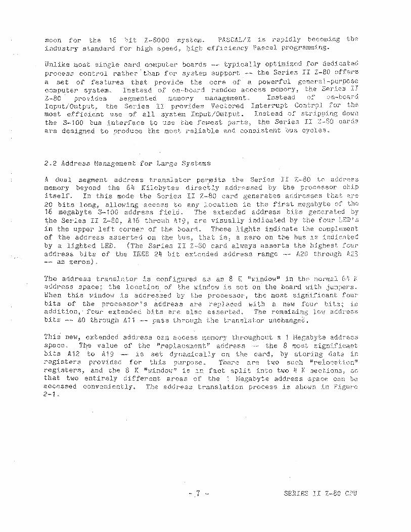
registers, and the 8 K nwindow n is in fact split into two 4 K sections, sothat twa entirely different ;:u~eas of the 'j !'1egabyte address space CaD beaccessed convenient The address translation process is shown in Figure2-1.
SERIES II Z-80 CPU
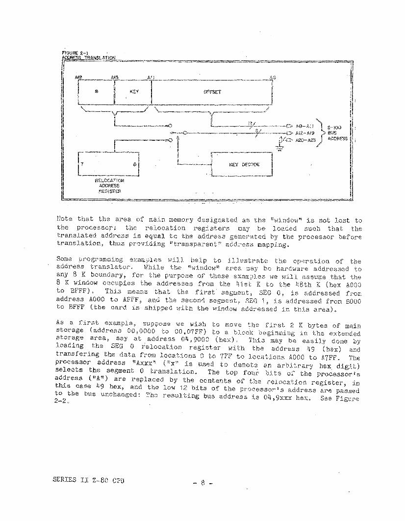
FIGURE 2-1 .
~~ .r~::!l~.."."'''_'h''''-"""",,;=o.=--.-_._,=,,-==<~._-::::..=-_=_=_=_.=:=====
RELOCATIONAOOHESS.REGISTER
Note that the area of main memory designated as the "window" is not lost tothe processor; the relocation registers may be loaded such that thetranslated address is equal to the address generated by the processor beforetranslation, thus providing "transparent" address mapping.
Some programming examples will help to illustrate the operation of theaddress translator. While the "1I'lindow U! area may be hardw'are addressed toany 8 K boundarYl for the pur'pose of these examples we will assume that the8 K window oocupies the addresses from the 41st K to the 48th K(hex AOOOto BFFF). This XJeans that the first segment, SEc.; 0
1is addressed from
address AOOO to AFFF, and the second segment~ SEG 1~ is addressed from BOOOto BFFF (the card is shipped with the window addressed in this area).
As a first example~ suppose lrJe wish to move the fi.rst 2 K bytes of mainstorage (address 00,0000 t.o OO,07FF) to a bloc'k begi.nning in the extendedstorage area, say at address 04,9000 (hex). This may be easily done byloading the SEG 0 ~elooation register with the address 49 (hex) andtransfering the data from locations 0 to 1FF to locations AOOO to A7FF. Theprocessor address i!Axxx li
(";){,Ii is used to df.m.ote an arbitrary hex digit)selects the segment 0 translation, The top four b.i.ts of the processor'saddress (IV A111) are replaced by the contents of the relocation register ~ inthis case 49 hex, and the low 12 bits of the processoris address are passedto the bus unchanged: The resu.l ting bus address is 04 i 9xxx hex. See Figure2-2.
SERIES II Z-Bo CPU
FlOORE 2'-;Iif.)(iM\IIR..E~
I\'IELOCA71OI'JADORfS3
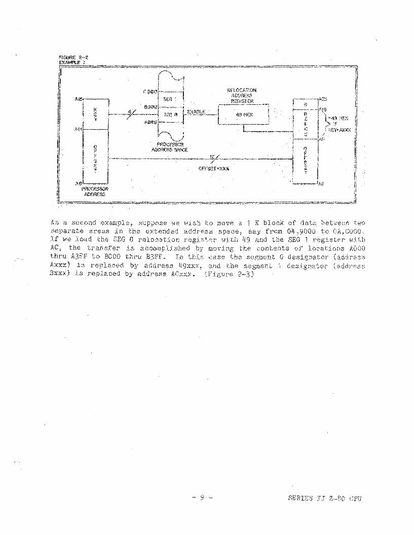
As a second example, su.ppose we l,rish to move a 1 K block of data bebJean twoseparate areas in the extended address space. say from 04,9000 to OA,COOO.If we load the SEG 0 relooation register with 49 and the SEG 1 register withAC, the transfer is accomplished by moving the contents of 100at:ioo.3 AOOOthru. AjFF' to BOOO thru B3FF" In this case the seg.ll1ent () designator (addressAxxx) is replaoed by address 49xxx l and tb.e segment 1 designator (addressBxxx) ~s replaced by address ACxxx. (Figure 2-3)
- 9 ~. SERIES II CPU
flGURE 2-:5~...E2,.....
..~_JPrograms may also be run in the extended stol"age area. In this ki.nd ofoperation the two segments may be grouped consecutively, giving a single 8Ksegment for the progl"Clm. Programs should be assembled to run at addressAGOO and should be less than 8K bytes in. length unless checking is done toassure that the program counter lrJon' t overf.lov,r back into m2.in. storage.
Even with these restrictions" this technj.que is extY'emely powerful formanaging a set of oVel~lays for a sophist:Lcated progran. All overlayprograms may be assembled to f'llD at address AOOG ~ .but any nuwber of overlaysmay be stored at random in the extended address space. Any of the storedoverlays may be actlva,ted by load5.ng the reloc2,tion rebi.sters id,th theappropr.iate pointers? and calling the overlay at address 11.000 ... Note thatany location in the main storage area may be directly referenced by thecurtent overlay, but that calls to other overlays should be routed through akernel which w.i11 switch the requested overlay tnto the Qap area, and switchthe first overlay back in on the return froID the requested funotion.
The !'ollowing programs are a simple set of subroutines which open either ofthe segments onto the specified areas of the system memory. note that theroutines do not limit the mappings to the extended storage area; anylocation in the first megabyte of memory may be accessed by these routines.For the purposes of simpliCity, these subroutines will al~ays consider thezero segment as an :!.nput file and the on€~ segment as an output file, though
SERIES II 2-80 CPU - 10 "..,

there is no physical reason why both the segments may not simultaneously beinput and output files.
The routines below initialize the ceoory management unit; open the input andthe output files, get the next byte from the input file; put the next byteto the output file; check for window overflow and correct the relocationpointers if overflow occurs; and will move up to 64 K bytes from anylocation in memory to any other.
These simple routines could easily be combined with others to providemuI tiple open files. searchi.ng. sorti.ng, overlay management, dynamic meJ:iloryallocation. and a variety of other sophisticated system functions.·
SERIES II Z~8() CPfT

MEHORY ~1ANAGEMENT SUBROUTINE;S
; DEFINITIONSIOBASE EQUREGO EQUREGl EQUBASE EQDKEYO BQUKEn EQU'
DEOA ;BASE ADDRESS OF ON-BOARD I/OIOBASE+2;ADDRESS OF RELOCATION REGISTER aIOBASE+3;ADDRESS OF RELOCATION REGISTER 1OAR ;HELOCATION POINTER FOR INITIALIZATIONDAGB ;SEGHENT 0 ADDRESSED AT AGOO HEXOBOR ;SEGHENT 1 ADDRESSED AT BODO HEX
,,;ENTRY POINTS AND VARIABLES
INIT : ,]HPOPNIN: .H1POPNOT: ,JHPGETB: ,JHP
PUTB: JHPNOVBLK: ..HlP
INITOOPNINOOPNOTOGETBOPUTBO1:-10VBKO
~
;.INPUT VARIABLESINBASE DS 3OTBASE DS 3LEN DS 2
;LOCAL VARIABLESSEGO DS 1SEGl DS 1INPTR DS 2OTPTR DS 2SEG DS
; SUBROUTINE INIT: INITIALIZE THE HEtmRY t1AlJAGEtlENd' UNIT; SUCH THAT THE SEGHElJTS POINT TO THE SA1,JE AREAS THEY PHYSICALLY;OCCUPY IN THE BAIN HEHORY, IN THIS 1t.TAY THE RELOCATION DEVICE;IS LOGIALLY TRANSPARENT TO THE SYST~l"
;USE A
INITO~ IN!OUTINROUTRET
Il,BASEREGOAREG1
; LOAD A "\rUTH BASE Jl.DDRESS OF SEG1·lENT 0; SETU P SEGHENT 0;A=BASE ADDRESS OF SEGHENT 1; SETUP SEGHENT '1;EXIT
SERIES II Z-80 CPU - 12 -
;SUBROUTINE OPNIN: OPEN AN INPUT FILE IN THE EXTENDED ADDRESS;AREA p BEGINNING AT THE ADDRr;;SS GIVEN IN THE H£feIORY LOCATIONS; CALLED INBASE. SET THE SEGNEIJT 0 HEGISTER InTH THE APPROPRIATE;OFFSET AIm SAVE AT SEGO. IlIPJiTR IS THE POIliTER TO THE FIRST;BYT£ OF THE INPUT FILE.;USE AjF~DpEsHpL
;FOru~T OF INB11.S£ IS INBASE=LEAST SINIFICANT BYTE, INBASE+l=;NID-SIGNIFICANT BYTE p INBASE+3=MOST SIGNIFICANT BYTE (NOTE;THA'f BITS 4 THRU 7 OF THE NSB NUS! BE O~S)
OPNINO: LDED
LDACALLSTAOUTHOlTOHINOVSHLDRET
INBASE ;1..,OAD DC !dlTH TlrJO LOVi ORDER ByTES OF;INBASE
INBASE+2;A::::HSB OF IUBASESPNT ;CALCULATE SEG AND OFFSET FROM A~D~E
SEGD ;SAVE SEGMENT POINTER AT SEGDREGG ;SETUP THE SEG~ffiNT REGISTERA,HKEYO ;INPNTR = AOOO+OFFSETH,AINPTR ;SAVE AT INPN'l'H
;EXIT
,; SUBROUTINE OPNOT: OPEN AlJ OUTPUT FILE BEGIlWING AT THE ADDRESS; CONTAINED AT OTBASE. SET THE SEGUEIJT 1 REGISTER HITH THE;RELOCATION ADDRESS AND SAVE AT LOCATION SEG1. THE POINTER;AT OTPTH IS THE .OFFSET THAT POINTS TO THE FIRST BYTE OF THE;OUTPUT FILE.;USE A.F~D,EpH,L
;SAVE AT OTPTH;EXIT
; OFFSETl1-BOOO KEYS FOR SEGl1ENT 1
OPNOTO: LDEDLDACALLSTAOUT110VORrnovSHLDRET
OTBASEOTBASE+2;LOAD A~D1E WITH ADDRESS IN OTBASESPUT ;CALCULATE RELOCATION AND OFFSETSEG1 ; SAVE RELOCA TI ON POINTERREGl ;LOAD HELOCATION REG FOR SEGl1ENTA$HKEY1H~A
OTPTR
SERIES II Z-80 CPU
;SUBROUTINE SPNT: CALCULATE THE RELOCATION P0I1~TER AND THE;OFFSET FOR LOADING TO THE HEHORY MANAGE~1EHT UNIT FROM THE;20 BIT JillDRESS CONTAINED IN A1 D,E (HSB TO LSB) ,;RETURN THE RELOCATION POINTER IN A AND THE OFFSET IN HL.;USE: A~F1DjE,H,L
1
SPNT: LXI1'10V'HHDANIHOVHOVILDAHET
OFHH,AL 1 £SEG
;HL POINT TO SEG;SEG GETS MID-BYTE OF BASE ADDRESS;ROTATE DIGITS USING A AND SEG;MASK BITS 4-7 OF OFFSET
;HL GET OFFSET;A GETS RELOCATION POINTER;EXIT
1
;SUBROUTINE GETB: GET THE NEXT BYTE FROM,AND INCREMENT THE INPUT POINTER, INPTR.;OVERFLOW AND RECALCULATE THE OFFSET AND;ADDRESS ON OVERFLOW.;USE A1 F,HL,DE,RETURN THE BYTE IN A.
THE INPUT FILE,CHECK FOR ~JINDO~i
SEGMENT RELOCATION
GETBO: LHLD INPTR ;HL POINT TO NEXT BYTEHOV D?M ;BYTE IN DINX H ;INPNTR=INPNTR+1MOV A?Hcpr KEYO+10H;CHECK FOR SEG~ffiNT OVERFLO\r,lJNZ EXGET ; NO OVRFLlJNVI H,KEYO jOVRFLW, RESET INPNTRLDA SEGOINR A ;SEGO:::SEGO+1STA SEGO ;SAVE AT .SEGOOUT REGO ; LOAD RELOCA nON REGISTER ~nTH NEW VALUE
EXGET: SHLD . INPTR ;SAVE POINTER TO NEXT BYTEMOV A?D ; RESULT IN ARET ;EXIT
SERIES II Z-80 CPU - 14 -
;SUBROUTINE PUTB: PUT THE BYTE IN A INTO THE OUTPUT FILE.;INCREMENT THE OUTPUT FILE POINTER, OTPTR. AND CHECK FOR;OVERFLOl,L IF THE POINTER IS OUT OF THE 4K ~iINDO\'l. RECALCULATE;THE RELOCATION POINTER AND THE OFFSET.;USE A,H.L
PUTBO: LHLD OTPTH ;HL POINT TO INSERT POSITIONMOV MiA ;STORE THE BYTEINX H ;OTPTR::::OTPTH+1MOV A,Bcpr KEY1+10H ; OVERFLOW?JNZ EXPUT ;NO, GO ONMiTI H,KEY1 ;RESET OFFSET ON OVRFLWLDA SEGlINR A ; SEG1;;: SEG1+1 ON OVRFLVlSTA SEGl ;SAVE NEIll RELOCATION POINTEROUT REGl ; LOAD THE RELOCATION REGISTER
EXPUT: SHLD OTPTR ;SAVE NEH OFFSETRET ;EXIT
;SUBROUTINE MOVBLK: MOVE A BLOCK OF DATA OF THE LENGTH GIVEN IN; LEN FRON THE ADDRESS GIVEN IN INBASE TO THE ADDRESS GIVEl~ IN;OTBASE. UP TO 64K BYTES MAY BE MOVED.;USE A,F,B,C,D,E1H,L
HOVBKO: CALLCALLLBeD
OPNINOPNOTLEN
;OPEN THE INPUT FILE AT INBASE; OPEIJ THE OUTPUT FILE AT OTBASE;Be GET LEHGTH COUNTER
NLP: CALLCALLDCXMOVORAJNZRET
GETBPUTB .BA,eBHLP
; GET THE NEXT BYTE;STORE THE BYTE IN THE OUTPUT FILE;LEN:::LEN-1
;BC;~O?
;NO~ GO ON;YES, EXIT
SERIES II 2-80 CPU
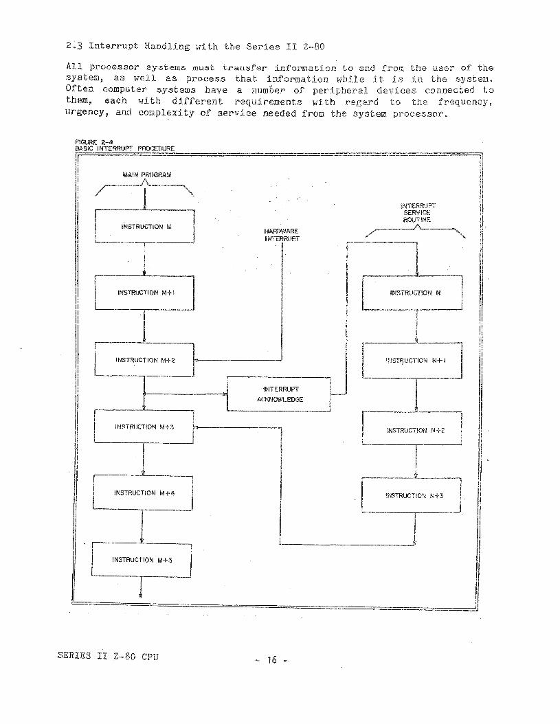
2.3 Interrupt Handling with the Series II 2-80
All processor systems must transfer information to and from the user of thesysteo p as well as process that information whi.le it is j.n the system.Often computer' systems have a number of per:Lpheral devices connected tothem, each with different requirements with regard to the frequency,uf'ganey, and cowplexity of service needed froo the system processor.
-----1-"
iNTERRUPTSERVICE.ROIJTINE
/"r-_.~-A_--""
-~~L~-'-T:: I!- !NST~UCT:::I
-~~~~CT'ON~
[==r=-lINSTRUCTIO~- I
----__J
HARDWAREiNTffiRUP.T
_ ..__J
-0----
INTERRUPT
ACKNOWLEDGE !~ -----l
/
L.-__'~P
MAIN PR'(lGRAM
I-~....---I-i\i-sr-R.....UCT'-: " l
INSTRUCTION M+2 }
INSTRUCTION M+3
'--
INSTRUCTI0::::J
INSTRuCTION-=:J
1
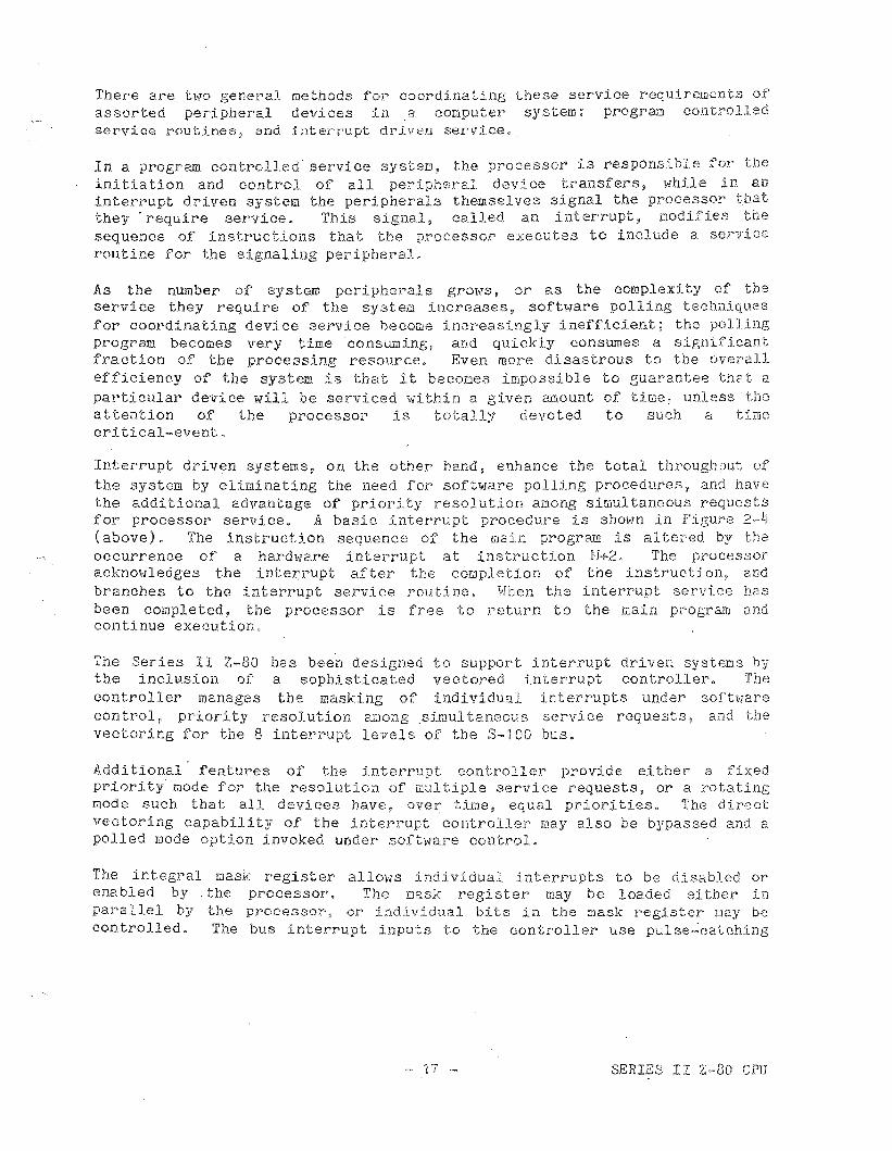
FIGURE 2-4BASIC INTERRUPT PROCEDURE
SERIES II Z-BO CPU - 16 ...
There are two general methods for coordinating these service requirements ofassorted peripheral devices in a computer system: program controlledservioe routines, and interrupt driven servioec
In a pr'ogram controlled' service system, the processor' is responsible for theinitiatIon and control of all peripheral device transfers, while in aninterrupt driven system the peripherals themselves signal the pk~ocessor thatthey 'require servicec This signal. called an interrupt. modifies thesequence of instruct.ions that the processor executes to include a serv1ceroutine for the signaling peripheralc
As the number of system peripherals grows 9 or as the comple::d ty of theservice they require of the system increases!, software polling techniquesfor coordinating device service become increasingly inefficient; the pollingprogram becomes 'lTel~y timeconsuming 1 and qUickly consumes a signif:i.cantfraction of the processing resource. Even more disastrous to the overallefficiency of the system is that it becomes impossible to guarantee that aparticular device will be serviced within a given amount of time, unless theattention of the processor is tota.lly devoted to such a ti.mecritical-event.
Interrupt driven systems, on the other hand, enhance the total throughput ofthe system by eliminating the need for softltlare polling procedures 1 and havethe additional advantage of priority resolution among simultaneous requestsfor processor service c A basic interrupt procedure is shown in Figure 2-4(above) . The instruction sequence of the main program is a1 tered by theoccurrence of a hardware interrupt at instruction lt~2. The processoracknowledges the intel~rupt after the cOKJpletJ.on of the instruction, andbranches to the interrupt service rout1ne. When the interrupt service hasbeen completed 1 the processor is free to return to the maj,n program andcontinue execution.
The Series II Z-80 has been designed to support interrupt driven systems bythe inclusion of a sophisticated vectored interrupt controllerc Thecontroller manages the masking of individual interrupts under softwarecontrol, prior1ty resolution among sj..mul taneous service requests, and thevectoring for the 8 interrupt levels of the S-100 bus.
Additional features of the interrupt controller provide either a ftxedpriority mode for the resolution of Qultiple service requests~ or a rotatingmode such that all devices have, over time~ equal priorities. The directvectoring capability of the interrupt controller may also be bypassed and apolled mode option invoked under software control.
The integral mask register allows incliv:Ldual interrupts to be disabled orenabled by . the processor. The ILI2.sk register may be loaded either .inparallel. by the processor, or individual bits in the mask register may becontrolled. The bus interrupt inputs to the controller use pUIse~catching
SERIES II Z-80 CPU
cireui t,'.:> to ;:~Iense interruptrequests will be accepted byignored.
l~eque s ts ~
the system.so tbat both one·-shot and stable
Narrow noise pulses, however, are
With this combination of featu1.'es p ' interrupt systems of any complexity mayeasily be implemented. The following sections desoribe the internalarch.itecture of the interrupt controller'. it,s command ;3tructure, and providea sample :i.nterrlll:lt servlce handler.
2.4 Z-80 Processor Interrupt Modes
The Z-BO processor chip has three basic modes of interrupt operation. whichmay be changed under software cant'ra1o The Series II Interrupt Controllermay be programmed to opera.te in anyone of these modes; Hade 2 ~ h01l1ieV(~r, isby far the most powerful and vel,"'satile~ and our programming examples will beconfi,ned to it 0
Hode 0
Uode 0 is identical to the interl"'upt response mode of the 8080 processorchip. In this mode the interrupttng dev:Lce places an instruction on theprocessor's data bus during the Interrupt Acknowledge cycle. The processorthen executes this instructlon instead of the next :Lnstruction in memory.In theory an;ir instruetion may be placed on. the data bus? but in practiceonly single byte instructions shol.11d be used because the 2-80 only producesan interrupt acknowledge cycle on the first byte of a multiple byteinstruction" The singlo byte call instructions! called Restarts, are theinstructions most often used in interrupt mode O. These instructionsexecute a call to one of eight fixed ~ocations in low memory, depending onthe particular eoding of the instruotion. The interrupt controller may beprogrammed to supply any of the Resta.rt ins'crucU,ons ion response to anyinterrupt"
Hode
1tJhen interrupt mode 1 has been selected by the programmel'~ all interrupts inthe system 1"ri11 be responded to by a caLL to lo:::ation 066 Hex. A cowmanservice routine and dispatch table should begin at that location if mode 1is selected.
SERIES II 2-80 CPU - 18 _
!'-lode 2
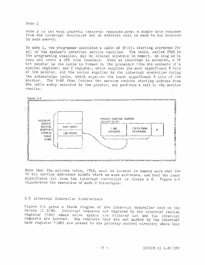
Mode 2 is the most powerrul interrupt response mode: a single byte responsefrom the interrupt contr~ller and an indirect call is made to any location:In main memory,
In mod~ 2 w the progran1m,er ma.i.nta:Lns a table of 16 -bit starting addresses forall of the system's interrupt service routines. The table. called ITAB inthe prograxIlming examples ~ may be located anywher-8 in memory, as lOl1,g as Itdoes not Cross a 256 bou.ndary,. IiIhen an interrupt is aceepted~ a 16bit pointer to t.he tabJJ:?o is formed the processor from the contents of aspecial ster. the I ster, which the most significant B bitsof the pointer, and the iTe(~tor s by the inter'Y'upt controller'the acknowledge e. supplies the least significant 8 bits of thepointer 0 The Z~80 then fetches the serviee routine starting address fromthe table entry selected the 9 and perfon:ns a call to the senric:eroutine.
DESIHED STARTING .I:;DDP.ESS
7 BITS FROMPEf:;:IPHERAL
I REGHIGH ORDER
IN1ERHUPTSERVICEROUTINE
STARTlfIIGADD,'tt:SS
TABLE(IT/I,B)
Note that the_ address table;, I'l'AB? wL1st be located in IJe.llwry such that the16 bit service addreSses -ahl~ys' "start on even addresses. and th.at the leasts.ign.ifi.cant b5. t from the i,nterr'upt controller is all"rays a 00 Figureillustrates the operation of mode 2 interrupts.
2.5 Interrupt Controller AY"chitecture
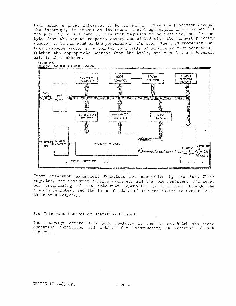
FigUJ.~e 2~6 g.ives a block d1agram of the 1nter'rupt controller used on theSerie,'3 II Z··80 0 Interrupt requests are captured by the interrupt requestregister (IRR) where noise spikes are filtered out and the interruptrequests are latchec,L requests that are not masked by tbe interruptrJask regJ.ster (H1H) are passed to the priori control cireul where
SERIES II 2-80 CPU
- . -_.
[~~ [;MODE f- I STATUS] I VECTOR I~~IS;~_-RESPONSE
REGISTER R~GISrl:R MEMORY
{,. J. ~ 4 Ii
11' ~ ~BUS "" 7- "
B'~~:<
.~ ~ .1\ ~
~ l? , i'
[ AUTO CLEAR I ! IN-SERVi~ r R:~::lREGISTER REGISTER
ill ~ '"~ 2>
ih l
'Ij ,A
INTERRUPT INTF..RRUPT .'"AO<
CONTROL -- PRIORITY CONTROLINTERRUPT
AJ INTERRUPTA-
REQUESTREGISTER
.~
'-- -r---"- REQUESTS
~ GROUP INTERRUPT
I- .. . .
wIll cause a group interrupt to be genera ted. Uhen the processor acceptsthe interrupt ~ .it Issues an interrupt acknowledge signal which causes (1)the priority of all pending interrupt requests to be resolved. and (2) thebyte from the vector response memory associated. 11ll th the highest priorityrequest to be asserted on the proces~oris data bus. The Z-80 processor useSthis response vector as a pointer to a table of service routine addresses,fetches the appropriate address from the table, and executes a subrolLtinecall to that address.
fiGURE 2-6INTERRUPT CONTROLLER BLOO( DIAGRAM
Other interrupt management functions are controlled by the Auto Clearregister, the interrupt service register, and the mode register. All setupand programming of the interrupt controller is exercised through thecommand register, and the internal state of the .controller is available inthe status register.
2.6 Interrupt Controller Operating Options
The interrupt controller I s mode register is used to establish the basicoperating conditions and options for constructing an interrupt drivensystem.
SERIES I1.Z-80 CPU - 20 -
Fixed or Rotating Priorities
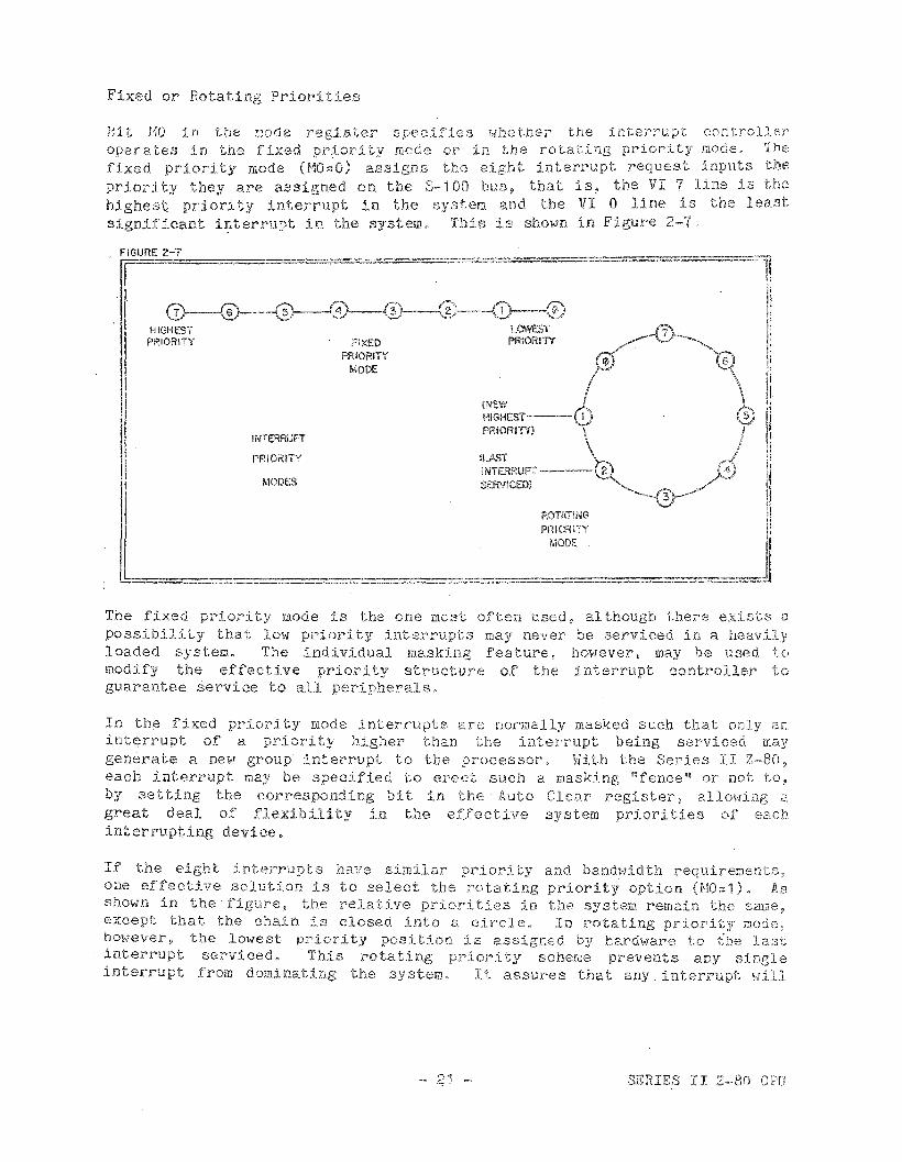
1~.1t 110 in thE: r~orje re Bter .spec5.fJ.e.s T.lfJether tr10 interrupt cODtrol1eroperates in the fixed priority mode or in the rotating priority mode. Thefixed prlority mode (MO=O) assigns the interrupt request inputs thepriority they are assigned on the S,,·, 100 blls that is, the VI 7 line is thehighest priority interrupt 1n the system and the VI 0 line 1s the leac'Jtsignificant ilfterrupt In the system. This 1,s sho'l-JD in F,igm'e 2-"'/"
FIGURE 2-1
@--@---@--(~}--~(~'-@'--'--'0-~-~)!·'iH-iHt.::i' tOWESTMIVI fiXED PRIORITY
PRIORITYMODE
II\1TERRUPT
PRIOR!TY
MODES
ROTATiNGPRIORITY
MODE
The fixed priority mode is the one most often used. although there exists apossibility that low priority interrupts may never be serviced in a heavilyloaded system. The indivj.dual masking feature~ however! may be used tomodify the effecti.ve priorHy str'ucture of the interrupt controller toguarantee service to all peripherals.
In th~ fixed priority mode interrupts are normally masked such that only aninterrupt of a priority higher than the interrupt being servioed maygenerate a new group interrupt to the processor. With the Series II Z-80,each interrupt may be specified to erect such a masking "fence" or not to,by setting the oorresponding bit in the Auto Clear register 9 al1ol"rir.lg agreat deal of flexibility in the effective system priorities of eachinterrupting device.
If the eight interrupts have similar prior1ty and bandwidth requirements,one effective solution is to select the rotating priority option (NO:1). Asshown in the· figure l the relative priorities tn the system Y'emain. the same,except that the ohain 1s closed into a circle. In rotating priority modehowever p the lO1"iBst priori poai Lion is assigned by hardware to t;he lastinterrupt se~'viced. This rotaUng priori.ty scheme prevents any s1 einterrupt from dominating the systemc It assures that any inter'rupt will
SERIES r I Z~>80 CPU
not have to 111!"ait more than seven lnterrupt oycles before be.ing servioed.Note that th~~re 1.s no nesting of interrupt,?} in the rotating mode; aLLpending interrupts are masked from the processor while an interrupt is beingserviced.
Common and Indiv.:Ldual Vectoring
Bit M1 in the mode register specifies whether the individual interrupts willbranch to different lOCations upon i.:"l,ceeptance of an interrupt I Ol~ whetherall interrupts wtl! branch to the 1:HUlle lOCEit:lon. the eOlIunon vectorlngmode~ the response associated th IREQO (VI 7 'w:Ul be asserted uponinterl~upt aekno"Tledge~ regardless of y,rhieh interrupt is beingacknowledged, The common vectoring mode j.s useful if aU service routinessave the total machine sta te bef"ore entering the actual device serviceroutine, In such a case~ the processor branches to the common register saveroutine, . then polls the interrupt controller to discover the highestpriority interrupt pending. and branches to the appropriate serviceprocedure. This approach avoids duplication of the register save routine,Bi,t M1::::0 selects the individ.ual vectOl~j,ng mode 'irJhHe ~1"1;;;: 1 selects commonvectoring.
Polled Node
Bit 2 of the mode l~egister allmllTs the system to d1sable the group interruptoutput from the interrupt oontroller. In the polled mode the processor mayread the status register in the interrupt controller to see if anyinterrupt requests are pending. and which request has the highest priority.Interrupt request bits may be cleared by software. The polled Qode optionthen bypasses the hal.... dHare interrupt. the vectoring and fencing functions ofthe interrupt controller while the request latching p masking, and priorityresolution remain unaffected. Bit H2::::0 selects the interrupt L1ode~ H2:::1selects the polled mode.
Haster Bask
Bit 7 of the mode register specifies the status of the caster mask bit ofthe interrupt controller, When the master mask bit j.s set, (1'17::::0) thecontroller is disarmed just a,s if all the mask blts in the mask register hadbeen set. lrJhen hit 7 is a 1 ~ thE:) chip is artJed and any unmasked actj,verequests will cause an interrupt output.
The remaining bits of the mode register specify (1) the polarity of thegroup interrupt output~. which is always aetive lOIN on the Sel~ies II Z-·80(1'-13::::0); (2) the polal~ity of the interrupt request signaJ.s~ '\,lh1ch is alHaysactive low in S-·100 systems (M4=O); and (3) the register pre-selectionaddress. These bits select whioh of the internal registers will be rea.d by
SERIES II Z-80 CPU
the prooessor during aof the data transfersection.
Status Registe,r
data readto and froJJJ the
['com thecontroller
contrallEn'.is g.iven .in
A Su.ITlElarya .later'
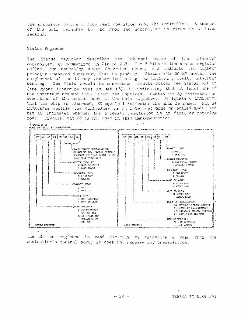
The Status 1"'egister descrJbes the lntel"nal state ofcontroller I as sur.m:narlzf.'d. i.nThe bits of the sta t.U[3
reflect the opera described above, and indicate thepriority unmasked int that is Status bits SO-S2 oontain thecOl1J.plement of the b;,irlar:v' vector" the st in.ter'rupending. The field should be cons:\.dered in,valid u.n1e38 the status btt(the group interl"'upt bit) :U, set ( ::.:1)? indioating that at least one ofthe interrupt request bits is set and unmasked. Status bit indicates thecondition of the master mask in the Mode register. S3 equals 0 indicatesthat the chip is disaJt'l.nedr. 33 equals 'p, ir1dieates th.e chip 1.3 ar1J1ed~ tindicates whether the oontroller is in interx'upt mode or polled mode, andbi t S5 lndicates \Mhether' tbe priori resolution is i.n fixed or rotamode. Fj_nally~ bit 36 .is not used in this implementation.
F!GlilRE 2-ftl,~~~;.rA~"'i!lll,;""T""Il.""~;,G;;""'=1MOm1=;"",_,,,,,,,,,,,,,,,,,~",,,,,,",,,,,,,,,,~_,_,,,_,,,,,,,,,,,,,,,m~,~~:'~~~,,=---;::;-...;T.~~...~"_~.--:.:="":l~:l<.:~~~
- ll,,"'T;;Tl~0 ~~~l
-1 ,-":;31
il i~1I"Jh.nlV '/[CV(lIiJ WJDiC~\1iIB!'1i 1111lCf rMUl~~1r.~i M n~'t! HHlP"l@::nrf ~H'MVrf\f
L". I>MMASIl[,1' an 'HMl' ~~ o\lCi' n~ 11'U'l,
VlliUD !l)NU1' \iM1£fM @'JI'n@
l' "--MAmr~ IMU,i\ £\II¥
iii ~,~ ilISMM[!lJ~ n C~-;l!fl AB'IMW
~-'--.---lloIn~~\li"7r MOO'lEIII 1i\l1[1I'I(~1j6"'F
!D l"Ol!\[!l
----~--~Il:mln MODi:!l\ <1~[1l
l ~ rW·f.f\'TH\~Q
.---·--·--·-----<!!MflI.1C INPtfi
@ ~~If" DIS-!\!lL[!lI eN11" [N,lIIilI..!D
----·--------.. I';Il\l\i,fill IIH[flfllJl"I·II 110 IJWMJ\!"'1EJTh
mil 1l!ll :;[1(;J /Jor lU,ST ~
UNM£SMf.~ Il'/llilleI!! flJ£1j'
~(O[l[
I!I ~II\HI
I jj()1'AYI~«,
L__'l,CI'O~ ~,n.cC'10'l
I1i II~IIIO'"""" V[CTMI ,;.oMMOl' VH.'"/()If,
1- ·,NIEI'IF%Jn &~OD[
@ INffl'llh.lNI I"OLL[O
~··_--....---l.aM1: P'OI.M'lln
!l ACHv( !JJWI ACli,f/: HIGM
----Ul.£lJJ POI..ARI1''If@ ACWIE lAW~ t1.C1~V[ il'HGH
G'fI[S[U,:C:lflO1ll :,'1
.,'.'~(?! Iftrr£fIHlo'Pi 5lD1hflOf ~t:,\UjTff~~
gil INI!:.,flVi"f f"Wi¥. Iq€GiS11W!~ @ ~NIT.P.AtJ1lO1· PtEoour:r ~fJ.f:lS1Ud
I I ,\lITO Ct.f.J\1l 1'liJ);1:r00l
1....-·_.._-..-.-_..-~-_ ..·_.--.MAlSl1EfI 1<'..$1( IlIO/iI) CHIP !lISllf'lMf.D
tollQIX£ ~I$'l"[M I. CHIP AfIl'&tT,
The Status registercontroller's control
is read direct executing a read from theit does not require any preselection.
SERIES II CPU
Interrupt Service Register (ISH)
The ISH is eight bits leng and is used to st~re the acknowledge status ofthe interl~upt requests.. lr1hen an inter'loupt is acknowledged, the controllerclears the associated l"equest bit and. sets the eorresp<md.ing bit in theISH. When the ISH bit is pr'ogrammed for' automatic clearj.ng~ t.he ISR bitwill be cleared before the end of the aclmoHledge sequence. If it is notset for auto-cll~cn'~ the ISB hit must be cleared by command from the Z=·80 0
Internally, the controller uses the ISH to erect a "masking fence n • When anISR bit is set and the fixed priority mode is selected, only an interrupt ofhigher' priority than the one being r.~1erviced "llil cause a J:1eltl interruptoutput, nesttng the lnterrupt irout:ines, and moving the masking fence up tothe new leveL NejA! interrupt requests of' a priority lower' than t,he onebeing serviced will be masked untn thE) ISH i8 cleared the Z-80. Whenthe Auto Clear is specified. no masking fence is erected, since the ISH bitis cleared during the ackno'loJledge sequence. The Auto-Clear funotion may be
. specified for each interrupt individually. by setttng the ,s,ssociated bit inthe Auto Clear register (ACR).
Information Transfers
There are two input/output ports associated with the interrupt controller -a control port and a data port. A read operation executed from the controlport will always read the status register, and a write to the control portHill ahlays 'loIl:"ite into the cmnmand register. IIhen a read or wri.te isexecuted. to the da.ta port~ l:lO"ilTever» the j.nfoI'Y.nation transfered depends onwhich of the internal registers has been pre-selected by the precedingcommand. During read operations» the Interrupt Request Register (IBR), theInterrupt Serv.ice Register (ISH). the Interrupt Mask Register (IMR), or theAuto Clear Register (ACR) are pre-selected for reading by the bits N5 andM6 of the mode Register. For writing into these registers, specific
. commands must be issued to the controller; the 1-15 a.nd 116 bits do notpreselect registers for writing.
2.7 Commands to the Interrupt Controller
The interrupt controller!s command set allows the Z~80 processor to selectand alter all the operating modes desoribed 'above, to customize thecontroller for (lif'fere,nt applications, Coruma.nds are entered into thecommand register by writing to the control pm-"/::.. In the cor.:u:nands describedbelow» lix,g indicates a IRdon! t care" btt position,
SERIES II Z-80 CPU
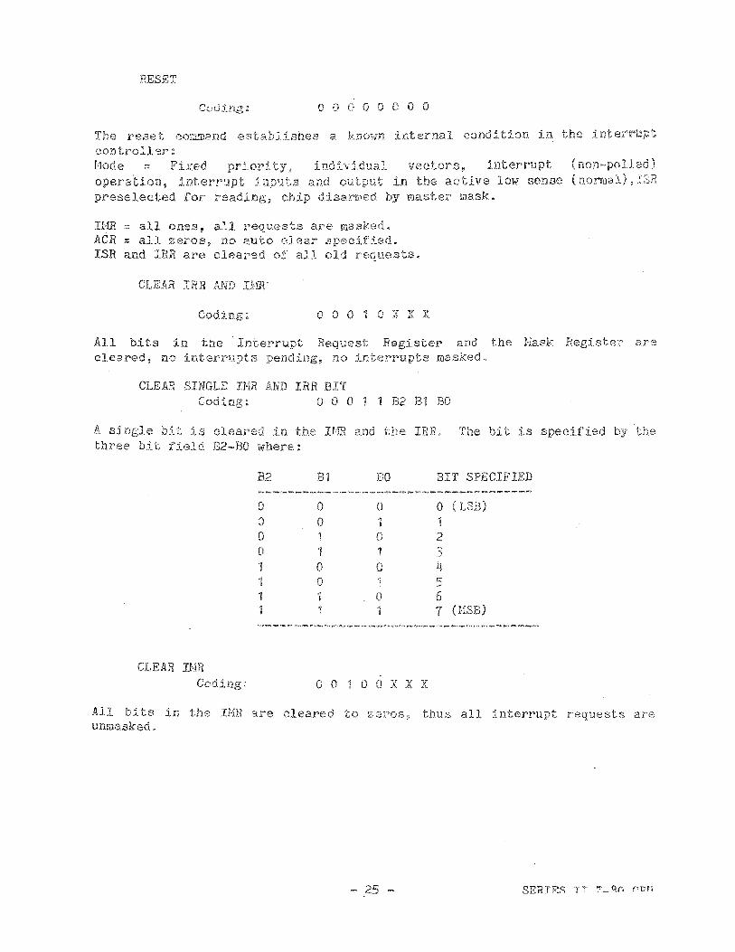
RESET
o a 000 000
condition in the int"""',r'iU"II'".kXlO:;W :internalThe reset conmand est;'";:,bli.shes acontroller~
110de ~, Fixed prlor:U,;y [I indivldual veetol~B~ interrupt (non-polled)ope.ration~ interrupt i s and Ow In the active low sense (normal) ~ ISHpreselected for w (:hip dj"sar'ID,"~d by master lilask.
1MR = all ones, all requests are masked.ACR = all zeros, no auto clear B
ISH and IBH are cleared of all old requests.
CLEAR IBR AND Itm'
Coding~ 000 1 0 X X X
All hits in the Inten'upt Request Register and the Hask Registel~ arecleared, no interrupts pending, no interrupts masked.
CLEAR SINGLE 1MB AND rEB BITCoding: 0 0 0 1 1 B2 Bl BO
fA. single bIt i.::; cleared in the nrn and the IRR, The bit is specified by "thethree bit field B2-BO where~
B2 Bl BO BIT SPECIFIED
() 0 0 00 0 1 10 1 0 2
1 31. 0 0 4"I 0 1 r,"
.)
1 0 61 1 or
( LSB)
(HSB)
CLEAR 1MBo OJ 0 (] x X x
All bits in the IHE are cleared to zeros~ thus all interrupt requests areunmasked.
- 25 - SERrR~~ TT 7_Afl 0ml
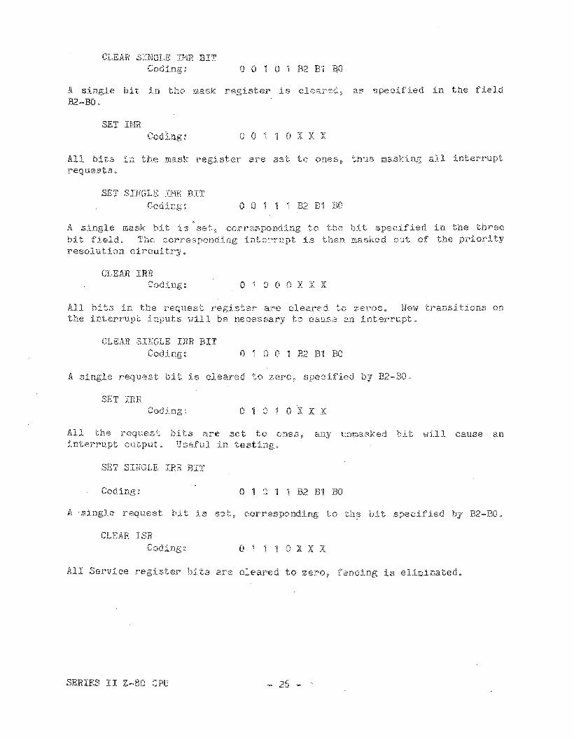
CLEAR SINGLE 1MB BITCodlng~ o 0 1 0 1 B2 B1 ao
A single b.a :l.n the mask reglster :is cleared p as speci.f:ied :in the field82-BO.
SET 1MBCod.ing~ 00 1 ~\ OXXX
All bits in the mask register are set to ones. thus masking all interruptrequests.
SET SINGLE nm BITCoding~ o 0 '! 1 1 82 81 80
A single mask bit is set. corresponding to the bit specified in the threebit field. The corresponding is then masked out of the priorityresolution circuitry.
CLEAR IHRCoding: O'iOOOXXX
All bits in the request register are cleared to zeros. New transitions onthe .interrupt inputs 1J>l.ill be necessary to cause" an interrupt.
CLEAR ,sINGLE IRR BITCoding~ o 1 0 0 1 82 B1 BO
A single request bit is cleared to zero, specified by 82-BO.
SET IRRCoding: 010'10XXX
All the requestinterrupt output.
bits are set toUseful in te
ones, any tU1masked bit ,,,il1 cause an
SET SINGLE IRR 8IT
Coding: o 1 01 1 B2 81 BO
A single request bit 1s set, corl~esponding to the bit specified by 82-BO"
CLEAR ISHCoding~ 01110XXX
All Service register bits are oleared to zero, fencing is eliminated.
SERIES II Z-81J CPU
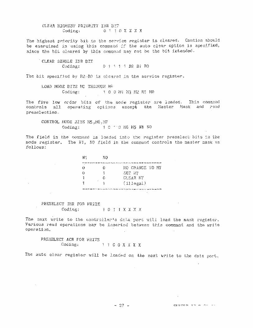
CLEAR HIGHEST PRIORITY ISR BITCoding~ 0 1 lOX X X X
The highest priority bit in the servioe register 1s cleared. Caution shouldbe exercised In us:lng 'this command if the auto clear option is specifJed!since the bit cleared by this command may not be the bit intended.
CLEAR SINGLE ISR BITCoding~ o 1 1 1 1; B2 B1 BO
The bit specified B2-BO is cleared in the service register.
LOAD HODE BITSCoding~
'fHROUGHo 0 H2 Hl iVlO
The five lowcontl~o13 allpreseleotion.
order bi,tsoperating
of the mode register are loaded. This commandoptions except the Haster I1ask and read
CONTROL HODE BITS H5 p1'16 ~r17
Coding: 1 0 1 0 H6 H5 N1 NO
The field in the command 18 loaded into the regj_ster preselect bits in themode register. The Nl ~ NO field in the command controls the master mask asfollows~
N'l NO
0 0 NO CHANGE TO 1-170 1 SET1 0 CLEAR N71 1 ( ill(~gal)
PRESELECT IHR FOR IflUTECoding: 1 0 1 1 X X X X
The next write to the controller I s data port will load the mask register"Various read opera.tions may be inserted betlrleen this coI'Il.tJ.and an,d the irlri teoperation.
PRESELECT ACR FOR WRITECoding~ 1 1 0 0 X X X X
The auto olear register will be loaded on the next write to the data port.
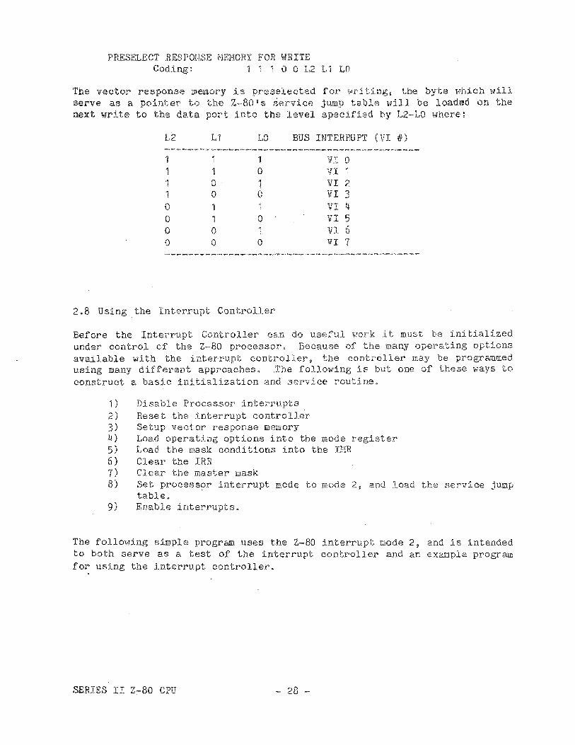
PRESELECT :RESPOnSE l'-mHORY FOR WRITECoding: 1 1 1 a 0 L2 L1 LO
The vector response memory is preselected for writing. the byte which willserve as B pointer to the Z-BO's ~ervice jump table will be loaded on thenext write to the data port into the level specified by L2-LO where:
L2
1111oooo
Ll
11oo11oo
10
1o1o1o1o
BUS INTERRUPT (VI #)
VI 0VI 1VI 2VI 3VI 4VI 5VI 6VI '7
2.8 Using the Interrupt Controller
Before the IntE~rrupt Controller carl do useful 11:ork it must be ini tiali.zedunder control of the Z·-80 processor. Because of the many opeY'ating optionsavailable with the interrupt controller~ the controller may be programmedusing many different approaches. .The folloWing is but one of these ways toconstruct a basic initialization and service routine.
1) Disable Processor interrupts2) Reset the interrupt controller3) Setup vector response memory4) Load operating options into the mode register5) Load the mask conditions into the IHR6) Clear the IRR7) Cleai the master mask8) Set processor interrupt mode to mode 2 i and load the service jump
table.9) Enable interrupts.
The follo1tling simple program uses the 2-80 interrupt Dode 2 i and is intendedto both serve as a test of the interrupt controller and an example programfor using the interrupt controller.
SERIES II Z~80 CPU - 28 -
HAJJDLE,nS"~
;; 'tHE FOLLO~iJIl>JG JrliOftflCIIIlJ:!;!.3Sg,"'UF,~
ON
p
~ nVDIV IDllftL; CONTROL.
VEGE,:SSA,RY PHClGRAl,)J"iIHG'1"0 'TlfVZ: OF VECTOHED
REGISTERS IN THE MAIN; SAVE:D UPON E1Ml"FlJC T'O [IN;UPON EXIT FROH .nn"EHHUPT"
THE Z- CPU AHE.1:,\ \\.)"1",1""",,11.»),\;:';' ~ llND HESJ:,'O,HED
~
~ DE,FINITIONS
( ANDFOE ~rEST HOU'I'INE:
J'BST HOUTINE;HERE.
AIJDHESS ON Z-·80 BOAHD
1000H
OEOH BASE:I0Ji3ASKfl·1 ;
STKHESTH'l'
l?P
IOBjL'3l:'~
ICONID,A,'I'
; ENTRY POI!\iTSOH(;,,H1P,J1>iP,)"NP SE~T'UPO
HaDE::POLL:SEHV:SAVE:EXT';' ~
,JHP<JFJP,,:I I'll',JNP
SAVEOE){]CTO
DB
DB 00
00
;00 MODE~, .INT NODE
8, POLLED HODEPHIOlUTY $, POI.LED HODE
INTERRUPT IN THEI DATA?~~VIO
IOlJ~lIJLL AUTO CLEARr:OHHESPONDIlifG INT: DA ETC.
SEHI:E;S II CPU
;TBE LOCATIONS OF THE INTERROPT SERVICE ROUTINES ARE STORED IN;THE JUMP TABLE BELOW" ITAB. CARE MUST BE TAKEN ~JHEH ORGiING;THE PROGRAM SUCH THAT ITAB NEVER OVERFLOWS A 256 BYTE BOUNDARY; IN MEMORY" AND THAT ITAB BEGINS AT AN EVEIl llEHORY LOCATION.
NOW
TEHPOTEHP1TEMP2
DBSET"ORGSETSETSETIFORGENDIF
o ,PSEUDO~OPS SO ITAB GOES$/2 ;AT RIGBT PLACE.NOW*2 ;=EV£N ADDRESS.$+OEH ;LAST LOCATION OF TENTATIVE ITAB.TEMPO&OFFOOH ;ISOLATE 2 MSBso$&OFFOOH ;IF THEY'RE TIiE SAME~
TEMP1~TEHP2 ;DON'T ASSEMBLE THIS CODE.TEMP1 ;OTHERWISE~ USE BOUNDARY
;FOR ORIGIN.
!TAB: ))t1f
D\<JD1IJDillDWDWDl~
DW
SERIES II 2-80 CPU
INTOINT1INT2INT3INT41NT5INT6INT7
;JMP LOCATION FOR VI 1 ROUTINECORRESPONDS TO LEVEL 0 ATVECTORED INTERmlPT CONTROLLERAND SO ON.
- 30 -
; SETUP SUBROUTINE: THE SETUP SUIBHOUTINE INITIALIZES THE 9519 ~
;LOADS THE OPERATING OPTIONS IN THE VARIABLES~ LOADS;THE RESPONSE HElMIOHY WITH VECTORS TO 'TIlE JU11P TABLE (ITAB) ~ AND;SETS THE 2-80 TO INTERRUPT MODE 20
SETUPO: D1H12LXIHOVSTA1XRAOUTCALL
HilIHVI
LDMEM: MOVOUTMOVOUTINRINRINRDCRJNZ
HVrOUTHVrOUTNVrOUTE1RET
HODEO: LDAORI.OUT
MVIOUTLDAOUT
HVIOUTLDA.OUTRET
H,ITABA~H
AICONHODEO
B·,OEOllC,B
BICOJl.~
A1,LIDATJLLB
LDHEM
A,ICONA~ OB
Ai OA9HICON
MODES
ICON
A»OBOHICONHASKSIDAT
A 1 0C011ICONCLEARSIDAT
; DISABLE JPHOCESSOR INTERRUPTS;SE1' PT ~~DE 2,HL THE JUMP TABLE; HIGH BYTE TO ACCUHULATOR.;1 REGISTER AINS HIGH ORDER PNTR; 11.:;:0i 11£S£'1' ') 9;S£1 THE CONTROLLER OPERATING MODES
; COHHANDS PRESELECT 11E~lORY LEVEL;LEVEL COUNTER ::::: 8; A ::::: PHESE:LECT NEXT LEVEL CONNAND;PHESELECT NEXT LEVEL;.A ~: L011J PNTR TO ,JUHP TABLE;IIJJUTE THIS MEHORY LEVEL
; ,:rm1,p TABLE PNTR ::::: NEXT ENTRY~ NE)(T LE'".EL,~
; DECna1:E:tJT LEVEL COUNTER;DONE FILLING K-fBHORY?
;CLE:AH nm
;CLEAR ISH
,CLEAR HASTER BASK PRESELECT IRR; ENABLE PfiOCESSOR INTERRUPTS;EXIT
, A~. ,". , •."" ."-'.1'.'
;HAKE INTO NODE SET COMNAND;SET MODE
; A := PH:l~SELECT £'1ASK COHHAND;; PHESELE\;T THE !1ASK REGISTER FOR HRITE; A. ~: !:'ll\.SK;;HRITE THE t-:iASK
; A - AUTO CLEAR PRESELECT COMl\IANDACH
;; A .~ AUTO CLEAR PATTERNptoJk~ITE AUTO CLEAR REGISTER;EXIT
"~ 311 ~" SERIES II Z~80 CPU
;HaDE 1 IS A SUBROUTINE WHICH CHANGES THE OPERATING HODES TO THE;VALUES CONTAINED IN THE VARIABLES AND RBINITIALIZES THE; CONTROLLER. IT IS TO BE USED DYNAHICALLYo CHANGE THE VALUES;AT MODgs" NASKS, AND CLEARS AND CALL r,lODE. THIS WILL CHANGE;1'HE OPERATING OPTIONS WITHOUT AFFECTTIl\lG rRR OR ISH".,MODE1 ~ D1
CALLE1RET
MODED;DISABLE INTERRUPTS; SET ~10j)E:S
;ENABLE INTERRUPTS;Exrr
; THE FOLLOiHNG SUBROUTINES ARE USED IF THE POLLED HODE;OF OPEHATION HAS BEEN SELECTED. A CALL TO POLL HILL RETURN; THE CARRY BIT CLEAR IF AN INTERRUPT REQUEST IS PENDING.; OTHERWISE THE CARRY WILL BE SET.;A CALL TO SERV WILL SERVICE THE HIGHEST PRIORITY INTERRUPT;THAT LS PENDING IN THE SYSTEM AND RETURN.; POLL. USES A &: F;SERV USES A»F,DE,HL."POLLO; TN
fiLeRET
SERVO~ INANIBLALXIADDl-lOVHOVINXMOVXCHGPC HI..,
SERIES II Z-80 CPU
ICON
ICON01H
l-l"ITflBLL»AE~H
l-lD»H
;INPUT CONTROLLER STATUS BYTE; PUT INTERRUPT PENDING FLAG IN CARRY; EXIT
;INPUT STATUS BYTE;r1ASK FOR LEVEL;OFFSET~LEVELlI\i2
; HL POINT TO JUHP TABLE;HL+OFFSET=VECTOR; HL~~VECTOR
;DE=ROUTIN~ ADDRESS;HL::::DE; JU)l.IP TO SERVICE ROUTINE
- 32 -
;ROUTINES SAVE MID EXIT: THESE ROUTINES ARE INTERRUPT SERVICE;SUPPORT ROUTINES" THE SAVE .ROUTINE SAVES THE MAIN REGISTER;BANK IN THE PROCESSOR CHIP~ RE.E:NABLES DJTERRUPTS 9 AND RETURNS;TO THE SERVICE ROUTINE" IT' NUST BE CALLED AT THE BEGINNING; OF EVEHY SERVICE' ROUTINE _.~
; START: SAVE;TBE EXIT ROiJTINE SIGNALS nm INTERRUPT CON'TROLLER nUT THE;SERVICE ROUTINE IS FINISHED p HESTORES THE HACHINE STATE~ AND! RETURNS TO TIlE INTERRUPTED PHOGRiU1 p OR: IN THE CASE OF POLLED;OPERATION~ THE: CALLING PROGRAH, EXIT SHOULD BE ENTERED BY A;Jl1P INSTRUCTION p ~nTH THE LoEVEL OF THE INTERRUPT BEING;SERVICED IN THE A REGISTER. SERVICE ROUTINES SHOULD BE;STRUCTURED p THEN;
START; CALL SAVE
(MAIN SERVICE ROUTINE)
.. 33 - SERIES II Z-80 CPU

;TEST PROGRAM~ THESE TEST PROGRAMS USE THE ABOVE ROUTINES TO;TEST THE OPERATION OF THE CONTROLLER IN.A SYSTEM. THE ROUTINES;LIGHT A BIT ON THE PROGI(lUifo1ED OUTPUT PORT OF THE;INTERSYSTEl:1S FRONT PANEL CORRESPONDING TO THE HOST RECENT;INTERRUPT SERVICED. THE S~1 VI "7 LINE COHRESPONDS TO A,LEVEL 0 INTERRUPT AT THE INTERRUp'r CONTROLLER, AND SHOULD;LIGHT FHONT PANEL PORT LIGHT O. A SHIPLE TEST OF THE; INTERRUPT SYSTEM IS TO RUN TEST AND GROUND EACH VI LINE IN;TURN, CHECKING THE PROPER FRONT PANEL LIGHT.JTHE TEST ROUTINES EXIT TO RESTRT 1tJHEN THE HOST SIGNIFICANT;FRONT PANEL SWITCH IS SENSED LO\'Il. PLTSTO IS THE POLLED;VERSION OF THE TEST ROUTINE WHICH OPERATES SI1"11LARLY.;THE STATE OF THE NEXT~'l'O-MOSl'-SIGNIFICANT FRONT PANEL; SWITCH DETERl'1INES WHICH ROUTINE RUNS -'- HIGH :;:; INTERRUPT TEST,; l.OW :':: POLLED TEST.
TESTO~ LXI SP!STK ;SET STACK POINTERXRA A ; ACCUHULATOR GETS o.OUT FI' ; CLEAR FRONT PANEL LIGHTSSTA MODES ; INTERRUPTS AND FIXED PRIORITY.CALL SETUP ; SETUP CONTROLLER.
HALT: IN FI' ;GET S\HTCHES.:liLC ;PUT D7 INTO CARRY,,·HJC RESTRT ; AND EXIT IF LOt;).HLC ;PUT D6 INTO CARRY.,JNC POLTST ;DO OTHER TES1~ IF D6 IS LOH.ltrL T ;HALT & WAIT FOR IlnERRUI'T,J~/1P HALT ;CONTINUE FOREVER
PLTSTO: LXI SP!STKIIT\lI 1\1 4STA HODES ;=FIXED PRIORITY~ POLLED HODECALL SETUPXRA A ;1\ := o.OUT FP ;BLANK LIGHTS"
1'1,TST1 : IN FI? ,GET SW ITCliE~:L
RL'C ,PUT D7 INTO CARHY.JNC f{ESTRT ;EXIT IF SVJITCH IS LOW. OTHERWISE,RLC ;PUT D6 INTO CARRY.,JC TEST ;GO TO OTHER TEST IF SHITCH IS UP.CALL POLL ,CHECK IF ANYTHING N~itl •eNC SERif ;YES? GO DO IT."HiP PLTSTl ;REPEAT,
SERIES II Z~80 CPU
; INTERRU PT SERVICE ROUTINES ~
INTO: CllLLHVIBVIJHP
INT1: CALLBVI1-1"1JHP
INT2: CALLMVIMIT IJHP
INT3: CALLMVIMVIJHP
INT~: CALLMV1BVIJHP
1NT5: CALLNV1BVI,JHP
INT6: CALLHVIHVIJHP
INT7: CALL!-lV1
MIT IJHP
SAVE
Ap 01HB~OINTSAVEA~02H
B w1INTSAVEA9 04HBp 2INTSAVEA?08HB9 3INTSAVEAp 10HB~4
INTSAVEAp 20HB,5INTSAVEA,40HB~6
INTSAVEAp BOH,B,1INT
;SAVE EllVIBOWlENT FIRST.;.11. GETS LIGHT PATTERN;B GETS LEVEL iff
;BRANCH TO CONHOH SERVICE ROUTINE
INT: OUTHOVJHPEND
FPApBEXIT
;UPDATE LIGHTS; A GETS LEVEL 11; RESTORE ~,lACHIJ.IlE STATE

2.9 Series II BUB Interface
Thfl SelR"iee II Z~80 provides a numbel~ of' operaUng options lrlhich g.ive theuJ!er Borne control over the procBssor-ta··buB :1.nterface 1 while stillaorrssponding to the IEEE bus . specification. These options includeproceSsor Bpe~~d selection of 2 or 4 ~mz and optional ad.d! tion of a singlewait state to all instruction fetch cycles (the instruction fetch oyc~e ofthe Z-BO processoI' is shorter than other memory cycles of the processor p andrepresents the worst case for memory access timea). all memory cycles, Orall I/O cyolEH:I.
In addition to these basic options a special feature has been included toallowl the implementation of extremely h:Lgh rel.iability systems. In order tomeet the IEEE standard for S~100 bus devices using a Z-80 processor, all busaddress and status signals should be latched. This is because the z-80 chipcan change its effective address at the end of an instruction fetch cyclewhile the bus read strobe is still valid. The IEEE specification oorreotlyP!~ohibits such timing ambiguities. To comply with this specification theSeries II Z-BO includes hardware latches on all address and status lines tothe S-100 bus.
There are two modes of operation of these latches: Partial Latching and FullLatching. Th~= Full Latch mode is designed for extremel;'( high reliabilitysystems w or operaUon in electrically noisy environments. The Full Latchmode halves the number of signal transitions On the bus and restricts allchanges In address and status signals to specific, non-criUcal parts ofthe bus cycle ~ thus drastically reducing btl.s noise and signal crosstalk.
The Full Latch mode decreases the effective merlOry access tiIJe of theprocessor'j requiring that either very fast memory boards be used (160 nsee.worst case board access for Ml cycles requires chip speed of approx. 125nsee in a typical design), or that a single wait state be added to all Mlcycles j slowing the processor approxim~tely 10'.
Other system parameters 1111111 usually reduce the vlai t state requirement toinsignifioance, but the occasional necessity for the faster Ml cycle can besattsfied with the Partial Latoh mode. This m'ode does not control signaltransitions as does the Full Latch mode p but provides for operation at 4 mHzwithout wait states if proper cycle triggerring is employed. AllInterSystems Series II memory boards 1,dl.l support no-walt operation at )-1
11Hz using the Part.ial La.tch mode.
SERIES II Z~80 CPU - 36 -

2010 Direct ~1emory Access Opera1:10ns
The last major feature of the Series II 2-80 concerns the relationship ofthe processor to Direct Memory Access devices on the bus.
The !:E:EE bus speoificatiOl.1 defines a special protoool f'Or the transfer' ofbus oontrol from a permanent bus master, in this case your Series II 2-80,to a' temporary bus master suob as a DNA device or attached peripheralprocessor. This protocol involves a specially timed and overlappedtransfer of the various signal groups on the bus such that the DNA devloeand the CPU are both d1~iving the most cri.tical bus lines in given i.nacUvestates during the transfer operation.
The circuit which controls this Uming could be included on. el ther theprocessor board or on the DMA board. It has been included on the Series II2-80 board. for two reasons: Fj.rst~ if it is included on the processorboard.~ it need not be duplicated on every DHA board .in the system~ andsecond$ sj.Dce no currently existing DBA boards include such. a c.ircuit~ :!.tis much easier to modify an existing board to meet the S-·100 standard Hthis circuit 1s centralized on the processor board.
The Series II 2-80 board~ then" contains a circuit which will conduct allthe timing of the bus transfer~ and tri·-state its own bus drivers accordingto the IEEE specifica.tion (sections 2.8.2.1 through 2.8.2,,4). m!A devicesmay sense the two bus transfer signa13~ XFER I and XFER II? on the SDSB lineand the CDSB line respectively,
The 2-80 also includes pull-up R~esistors on the four DBA arbitration lines p
30 that they need not appear else~lhere in the system, and 10 ohm resistorsin series 'itlith the control output lines, to prevent dr:Lver fatigue a.ndglitches during the overlapped bus transfer.
- 31 - SERIES II 2-80 CPU

SERIES II 2-80 CPU - 38 -
Sect.ion 3.0
Board Setup
3.1 Bus Interface SetupSelecting the Processor SpeedSelecting the Latch ModeAdding Single Wait StatesNon-Maskable Interrupt SetupStandard Bus Interface Configuration
3.2 The On-Board EEPROH and Automatic BootstrapEPROM Type SelectEPROM and Jump Address SelectionEnabling the EPROH and .JumpEPROM Wait States for 4 mHz. OperationInterSystems Standard EPRrn1 Configuration
3.3 Input/Output Port SetupI/O Base Address Selection
3.4 Vectored Interrupt Controller SetupUsing an Off-Board Interrupt Controller
3.5 Memory Management SetupLocating ·the Address Translator in Nain HemoryStandard Hemory Nanagement Configuration
3.6 Front-Panelless OperationMemory Mrrite Strobe GenerationFront-Panel Control StrobesFront Panel Header in Front Panelless Systems
3.7 Summary of the Standard Setup
3.8 Jumper Summary
3.9 Installing the Board in Your System
- 39 .. SERIES II Z-BO CPU
SERIES II Z-80 CPU
====.. 11I
0::W
o ....JO::....J
"'(§~-1:01-
Z1 0ttu0-
>
This section or the manual describes how to set up the Series II Z-80 foroperation in your system. Ce!~tain jumpers on your board are only used inaiSsembly or in testing'w and these will be described only in thereference section.
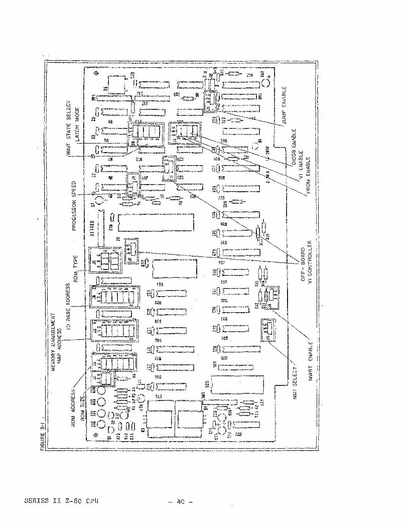
Figure 3-1 shows the board location of the jtllIJpers we are concerned ~d th inthis section.
3.1 Bus Interface Setup
The first and most important ohoice in the setup of the 2-80 board is theselection of processor speed. Either 2 HHz or )-\ HHz operation ma.y beselected 'iJlfith the jumper ,1G" The choj.ce of processor speed is acomplicated decision iJr.l'\fOlvJ.ng the access times of the other boards in thesystem~ the latch control mode selected w and the use of wait states o
Table 3-1 gives the various acoess times associated with the different typesor processor cycles at 2 ?J.Jd 4 t'1Hz l' for the full and partial latchi.ngmodes, Note also that the effecttve access time differs fOj:' static anddynamic or edge.·triggered devices, This is because an edge-aotivated devicesuch as a dynamic memory must. Ha1t to begin its cycle untH certa:Lninformation is guaranteed to be valid, whEe static devices respond toaddress changes as fast as possible. and do not require a strobe signal tobegin their cycle.
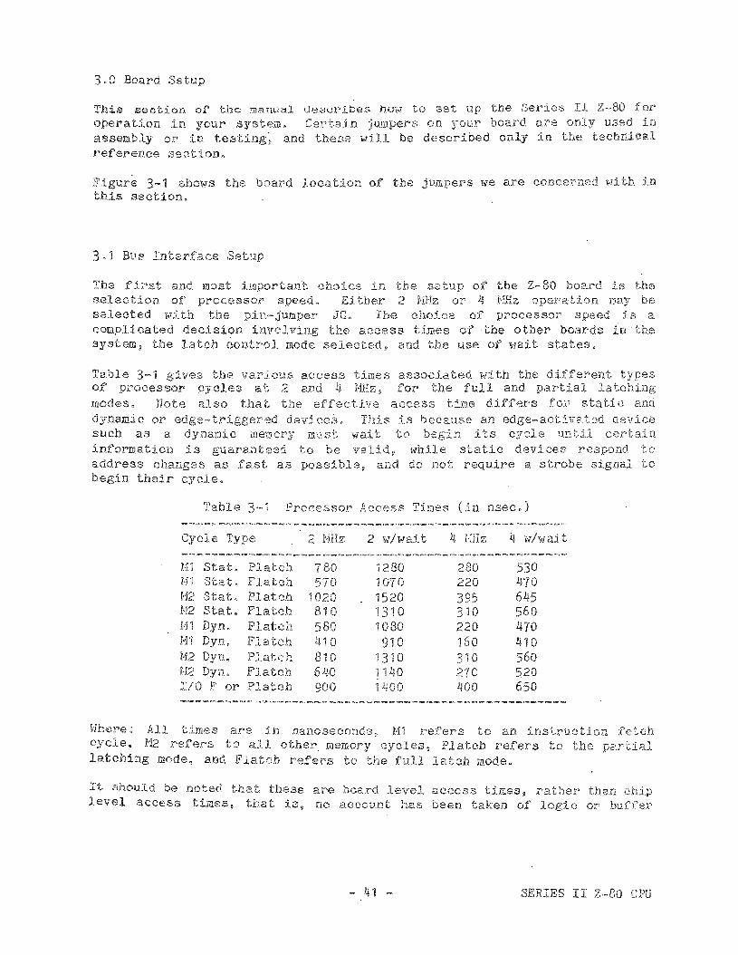
Table 3-1 Processor Access Times (in nsee.)
Cycle Type 2 NHz ') IIf/wait )~ tHz 4 whrlaHc:
~---~~-~---~~~~-~--~-----~-~~~~~~~~-----~~~~~---~~-~
Nl Stat. Platch 780 1280 280 530H1 Stat. Flatch 1070 220 lnoH2 Stat. Platch 1020 '1520 395 645H2 Stato Platab. 810 1310 310 560H1 Dyn, Platen 580 1080 220 1170H1 Dyn, Flatcb. 410 910 160 410X'J/2 Dyn. P.latch 810 1310 310 560Hc~ Dyn" Flaten 6l.j·O 1140 270 520I/O F 01" Platch 900 11100 ).[00 650
Hhelre ~ AIl tJm8s a.re j.n na.noseoonds, HI rE,fers to an instruction fetchcycle" H2 refers to all other memory cycles, Platch refers to the partiallatching mode, and Flaten refers to tb.e full latch mode.
It sJ:lOuld be noted that these are board level access times, rather thanlevel aocess times. that is, no account has been taken of logic or buffer
SERIES I I Z,-tlO CPU
delays on the memory board but full worst case delays on the processor havebeen included in the calculations.
It CBn be BeeD that the correct choice of bus cycle depends on a variety oft~ctor~. The most reliable bus cycle is the fully latched cycle. but accesstimee Bra considerably Shorter, especially for H1 cycles which are alreadyl~hort in the Z=80. It is therefore recommended that if the full latch wadeis used at 4 MHz; a wait state be added to all M1 cycles. This will slowthe operation of the processor approximately 10%. but. allows the use of 300nsee. static memory boards and 250 nsec. dynamic menory boards with ease.Adding a wait state to all memory cycles and using, the full latch modeallows the USl;; of less expensive ,1~50 nsee. static or 1+00 nsee. dynamicmemory boards~ but slm~s the processor by 25%.
Full speed 4 HHz operation should' use 'the partial latch mode. HhHe thismode creates somewhat mOl~e bus noise than the full latch mode~ it allowsthe use of 250 nsee. static memory boards~ and 200 nsec. dynamic oredge-activated memories without wait states. (Note: The above calculationsfor edge-activated and dynamic memory boards in the partial latch mode arederived using the rising edge of the PSYNC signal as an address valid strobeto start the tlemory cycle, aborting the cycle later if it is an I/O cycle.In the full latch mode the start cycle trigger is the IEEE address andstatus strobe. STVAL.)
Selecting the Processor Speed
Pin-jumper JG selects the processor speed. It is located on the right sideof the board between U5 and U10.
Processor Speed, JG
Selecting the Latch Mode
2 HHz.4 NHz.
B to CA to B
The latch mode of the processor is selected at pin-Jumper JH-1, located onthe right side of the board between U12 and U13.
Latch Mode~ JH-l
SERIES II Z-80 CPU
Full latchPartial latch
B to CA to B
Adding Single Wait States
A single wai t state may be added to any instruction fetch. any l11emo!'y(lncluding lnstruction fetch cycles). any 1/0 cycle, and any referen(:~e tothe on-board EPROM. 'The addition of these wait states is controlled bypin~juxllpel~s ,JH-2 through ,JH-5. also located betv,reen U12 and U13, It shouldbe noted that~ for 4 MHz operation 9 all standcu'd EPHOI1 cO:cJponents urillrequire a wait state for correct operation.
Wait State Selection. JH-2 thru JH-5
Cyole Type ,,Jumper 1 waH no-wait----~~~~~~~~--~-------~-~---~~-~-~~~~-~-~
I'll ,JH·-2 A to B B to CAll Hemory ,JH-3 fA to B B to CAll I/O JH-!'! A to B B to COn-board EPROM ,JH-5 A to B B to C
Non-Maskable Interrupt Setup
The last setup we are ooncerned wHh in the bus interface section is theconnection of the non-maskable interrupt line. This line, as yet unused inmost 3-100 systems, may be conneoted to either the 111'11 line on the S-,100bus, Or to the Power Fail Pending line, or disconnected from the system.
If you are uslng a Pot·,rer Fail anticipation c j.rcuH, and support the cirouitwith software routines that respond to an NI:-11 as a power fail p then connect1IT1I to Power Fail.
If you have some other use' for the Non-Maskable Interrupt, then it should beConnected to its Oim pin on the bus. If you do not use the line in yoursystem p disconnect the NfI-U line from the bus entirely by removing the shuntfrom the IN pin-jumper.
Non-Maskable Interrupt, IN
mlI to NM1NMI to Power FailNo NHI to Bus
A to BB to C
OPEN
SERIES II 2-80 CPU
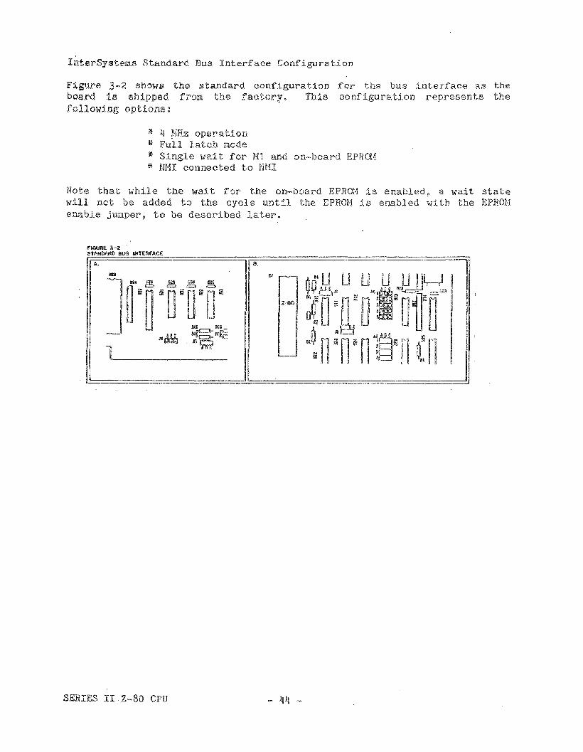
InterSystems Standard Bus Interface Configuration
Figure 3-2 Sh0101S the standard configuration for the bus interface as theboard 1s shipped from the faotory. This oonfiguration represents thefollowing options:
~ 4 ~Hz operation* Full latch mode* Single wait for M1 and on-board EPRa4~ NMI connected to NMI
Note that whil<:l the wait for the on-board EPROH is enabled? a wait statew:lll not be added to the cycle until the EPROH is enabled with the EPROHenable jumper~ to be described later.
fIGURE ,1-;::STANOIIRO (jUS INTE!1f~ _
8.
l-ao
SERIES IIZ-80 CPU
3.2 The On-Board EPRON and Autowa tic Bootstrap
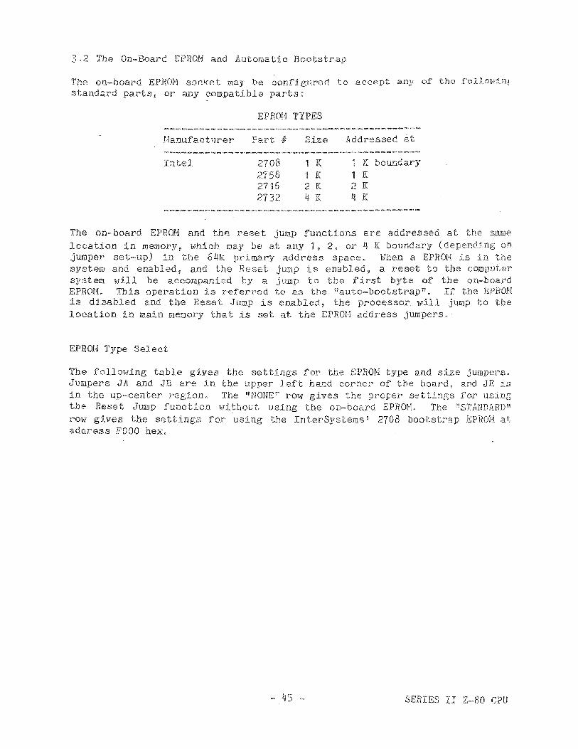
The on--board EPRON Bocke t may be oonfigured to accept any of the t'ollm·,inistandard parts~ or ;,:my compatible parts;
EPROH TYPES
Hanufacturer Part ff Size Addressed at
Intel 2'708 1 K 1 K boundary2'758 1 K 1 K2'716 2 K 2 K27 )4 K 1! K
The on-board EPRON and the reset jump functions are addressed at the SBJ118
location in memory ~ which may be at any 1. 2, or 1.* K boundary (depending onjumper set-up) in the 64k primary address space. lIlhen a EPRON is in thesystem and enabled. and the Reset jump is enabled? a reset to the computersystem will be acoompanied by a jump to the first byte of the on··boardEPRON. This operation is referred to as the l1auto-bootstrapil, If the EFRONis disabled and the Reset Jump is enabled. the processo~ will jump to thelocation in main memory that is set at the EPROl·l address jumpers,
EPROM Type Select
The follOWing table gives the settings for the EPROM type and size jl~pers.
Jumpers JA and JB are in the upper left hand corner of the board, and JE isin the up-center region. The "NONE" row gives the proper settings for usingthe Reset Jump funotion t,rithout. usj.ng the on-board EPROH. The i'STANDARDiVrow gives the settings for using the InterSystems ' 2708 bootstrap EPROM ataddress FOOD hex,
- J.j5 - SERIES II Z-80 CPU
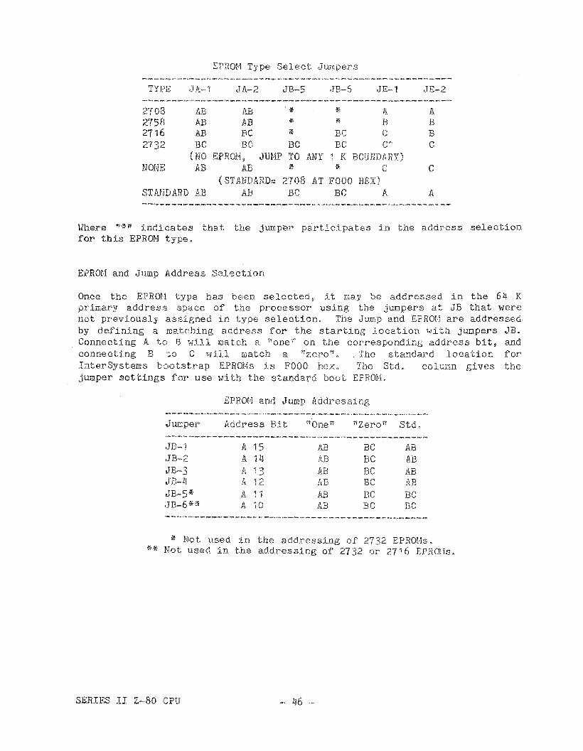
EPRm1 Type Select ,Jumpers
TYPE ,J A···' JA-2 ,JB-5 ,JB-6 JE-l JE-2---~~.~-~~-~-~-~=~~~~~~--~-~~-~~~~--~-~----------------
2708 AB AB ';Ii * A A2758 AB AB '* "* B B2716 AB Be Me Be c B2732 BC Be Be Be c
(NO EPROl'1, J'UMP TO ANY 1 Ie BOUNDARY)NONE lIB AB i * C C
(STANDARD=. 2708 AT FOOD HEX)STANDARD AB AB BC Be A A
\lhere fII*n indj.eates that the jump~r participates in the address selectionfor this EPROM type.
EPROH and Jump Addl"ess Selection
Once the EPROH type has been selected 9 j.t may be addressed in the 64 Kprimary address space of the processor using the jumpers at JB that llierenot previously assigned in type selecti.on, The Ju.mp and EPROH are addressedby defining a matching address for the starting loce.tion with jllIJpers JB.Connecting A to B will match a lione ll on the corresponding address bit, andconnecting 13 to C will match a "zero n • The standard location forInterSystems bootstrap EPROHs is FOOO heJL The Std. column gives thejt~per settings for use with the standard boot EPROM.
EPROH and ,Jump Addressing
,Juraper Address Bit "0ne " "Zerol! Std.-~~~-~~~-~-~------~~~--~-~~~~--------~~~---~~
,JB-·l A 15 AB Be 1\.13,JB-2 A 11~ 1\.B Be AB,JB-3 A 13 1\.13 Be 1\.13,JB··4 1\. 12 AB Be AB,JB-5* A. n 1\...'3 BC Be,JB-6~H'r A 10 AB BC Be
*' Not used in the addressing of 2732 EPROUs .•• Not used in the addressing of 2732 or 2716 EPRals.
SERIES II 2-80 CPU - lj·6 .-
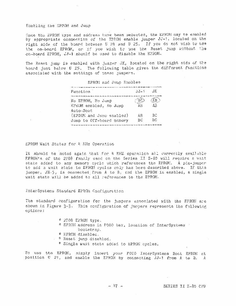
Enabling the EPROH and ,Jump
Onoe the EPRON type and addreSB have been selected. tIle EPROH may be enabledby appropriate connection of the EPROM enable jumper ,JJ-1, located on theright aide of the board between U 24 and U 25. If you do not wish to usethe on-boal.~d EPROM~ or 1f you w:lsh to use the Reset jump without theon-board EPROM~ JJ-1 should be used to disable the EPROM.
The Reset jump is enabled ldtb jumper JK? located on the right side of theboard just below U 25. The following table gives the differentassociated with the settings of these jumpers.
EPROH and Jump Enables
Funct:Lon
No EPROM, No JumpEPROM enabled ~ No ,JumpAuto-Boot(EPROM and Jump enabled)Jump to Off-board memory
EPROM Wait States for 4 MHz Operation
JJ·-·l
AB
ADBC
AB
BCBC
It should be noted again that for 4 l~H.Z operation all currently avaHableEPROH's of the 2708 fam:Lly us(~d on the Series II 2-80 will require a ii/aftsta te added to any memory cycle \1h].oh references the EFRON. A pin-·jumperto add a wait state to EPROH cycles only has been described above. If th1sjumper~ JH~5 ~ 1s connected. frow A to E, and the EPROM is enabled, a singlewait state will b·e added to all references to the EFRON.
InterSystems Standard EPRor·j Configura. tlon
The standar'd configuration for the jLUllpers associated iorith the EPRml areshotm in FiGure 3··30 This configuration of jUrJpers represents the followingoptions:
* 2708 EPRON type.'" EPROll address is FOOO hex, location of InterSystems
bootstrap.* EPROM disabled.• Reset jump disabled.• Single wait state added to EPROM cycles.
To use the EPROH 9 simply insert your FOOO InterSystems Boot EPROl"! atposition U 21 ~ and enable the EPROM by connecting JJ-1 from A to B. A
SERIES II 2-80 CPU
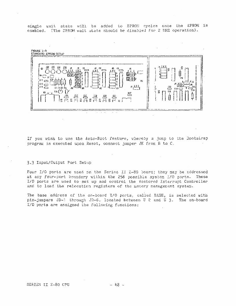
single wait state will be added to EPROn cycles once the EPRON isana.bled. (The EPROM wait sta te should be disabled for 2 rIHZ opera.tion).
If' you wish to use the Auto-Boot feature 1 whereby a ,jump to the Bootstra.pprogram is executed upon Reset~ connect jUDper .JK from B to C-
3.3 Input/Output Port Setup
Four I/O ports are used on the Series II Z-80 board; they may be addressedat any four-port boundary within the 256 possible system I/O ports. TheseI/O ports are used to set up and control the Vectored Interrupt Controllerand to load the relocation registers of the memory management system.
The base address of the on"·board I/O ports~ called BASE, ispin-jumpers .JD-1i throue:;;h JD-6! located bebJeen U 2 and. U 3.I/O ports are assigned the following functions:
selected withThe on-board
SERIES II Z-80 CPU - 48 -
Ta,ble 3··3 I/O Port Functions
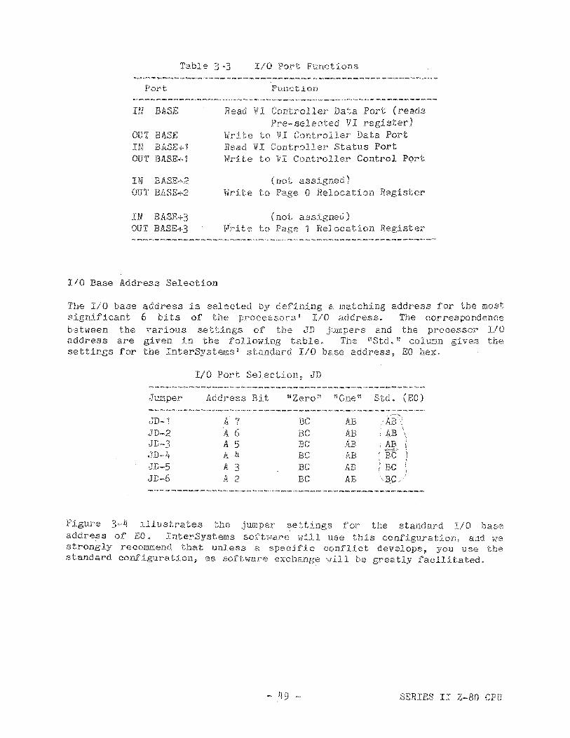
Function
IN [lASE
OUT BJ\..SEIN BASE+lOUT BASE+1.
IN BASE+2OUT BASK+-2
IN BASE+3OUT BASE+3
I/O Base Address Selection
Read VI Controller Data Port (readsPre-selected VI register)
Write to VI Controller Data PortRead VI Controller Status PortWrite to VI Controller Control Port
(not assigned)Write to Page 0 Relocation Register
(not assigned)lAT~rite to Page 1 Relocation RegisteX'
Tbe I/O basesignificantbetween tl1eaddress aresettings for
address is selected by defining a matcbing address for the most6 bits of the processors g I/O address, The correspondencevarious S8 t tings of the JD jurn.pers and the processor I/Ogiven in the following table. The "Std. flU coluEln gives thetbe InterSystems' standard I/O base address p EO hex.
LID Port Selection, JD
Jumper Address BH "lero" "Cne" Std. (EO)
JD-1 A 7 Be AB,JD-2 A 6 BC AB ABJD-3 A S BC .AB ABJD-4 A 4 BC AB 'BeJD-5 A 3 Be AB BeJD-6 A 2 Be AB
Figure 3-4 illustrates the jumper ~ettings for the standard I/O baseaddress of EO. InterSystems software will use this configuration. and westrongly recommend that unless a specific conflict develops~ you use thestandar>d configuratiol1 p as softMare exchange ~lill be greatly facilitated.
- }.J9 - SERIES II l-80 CPU
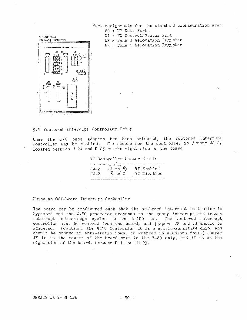
Port assignments for the standard configuration are;EO _ VI Data PortEl = VI Control/Status PortE2 - Page 0 Relocation RegisterE3 = Page 1 Relocation Register
3.4 Vectored Interrupt Controller Setup
Once the 110 base address has been selected? the Vectored InterruptContl~ol1er may be enabled. The enable for the controller is jUIJper JJ~2~
located between U 24 and U 25 on the right side of the board.
VI Controller Master Enable
JJ-2,JJ-2
VI EnabledVI Disabled
Using an Off·-Board Int.errupt Controller
The board may be configured suoh that the on-board interrupt controller isbypassed and the 2-80 processor responds to the group interrupt and issuesinterrupt acknmdedge cycles to the 3-100 bus. The vectored interruptcontroller must be removed from the board, and jumpers JF and JI should beadjusted. (Caution: the 95'19 Controller Ie is a. static-sensitive chip, andshould be stored in anti-static foam, or wrapped in a.lUt:linUlll foiL) JumperJF is in the center' of the board next to the 2-80 chip, and JI is on theright side of the board, between U 11 and U 23.
SERIES II Z-80 CPD
Bus Interrupt Enables
Function
BUB Into AcceptBus Int, Assert
LocalController
11 to CB to G
ConventionalInterrupts
fA to BA to B
If these jumpers are not installed, or if they are connected from B to C,they enable the vectored-interrupt controller circuitry.
3.5 Nemo.ry Managem1:,mt· Setup
A number of options exist in the setup of the address translator:(1) Eitber a single 4 K relocatIon page or 2 independant 11 K relocationpages may be selected. (2) The relocation lIirlindow" may be located anywherein main memory. (:3) The EH1tlre address translator may be enabled ordisabled with a master enable jwoper.
The following table gives the settings for the number of pages and themaster enable jumper. The InterSystems standard configuration is to enableboth !.j K pages.
Address Translator Size and Enable
Function ,JC-5 JC-6
Single 11·[ pagE) iff: AB BeTHO i.j.I{ p"lges Be BC Be
Translator Disabled X X AB
lilhel"e iH{;Vf indicates that th1s jw:n];')er' participates in the address decoding 9
and "Xn indioates a "don't care" setting.
Looating the Address Translator in Main Memory
Once the size of the translation window has been selected, it may be lOCatedin main memory on any Ii K boundary if the window size is 4 Ie, or on any 8 Kboundary if both ij K pages have been enabled. If the translator has beendisabled the master enable jtUDpex', JC,-6 1 the setting of these adclre,ssjumpers is insignificant.
The translator is addressed by defining a match address for the first byteof the window area with JC-1 through JC-~. The following table gives the
SERIES II CPU
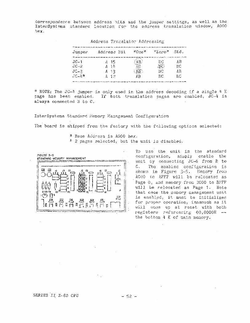
6orrespondence between address bits and the jumper settings, as well as theInterSystems standard location for thl:" address translat.ion 'i<lrindow" AOOOhex.
Address Translator Addressing
Jumper Addre:;:H~ Bit "Gns uu ~!Zeroml Std"
J'e,", » A 15 ABJC-2 A III BeJC-3 A 13 ABJC-4* A '12 AB Be Be
~ NOTE: The J'e'"·lI jumper is only used in the address decoding if a single }-i Kpage has been enabled. If both translation pages a.re enabled~ ,JC-1.I isalways connected B to C.
InterSystems Standard Hemorjl' f1anagement Configuration
The board is sb.ipped fk'orn the faetory 1i1T1 ttl the fo11o~.oJing options selected:
* Base Address is AOOO hex.• 2 pages seleoted. but the unit is disabled.
To use the unit in the standard()onfigul'a tion, siDlply enable theunj,t by conneoting JC·_·6 from B toC. The enabled configuration isshown j.D Figure 3-5. j'leDory fromAOOa to klFFF will be relocated asPage 0, and memory from BODO to BFFFt,ri11 be relocated as Page 1. Notethat once the memory L2anageDent unitis enabled. it must be initializedfOJ:' proper operatioD., inasmuch as itt'll1J. coos up at reset l1lith bothregisters referencing OO,OOOOHthe bottom 4 K of wain memory.
SERIES II 2-80 CPU
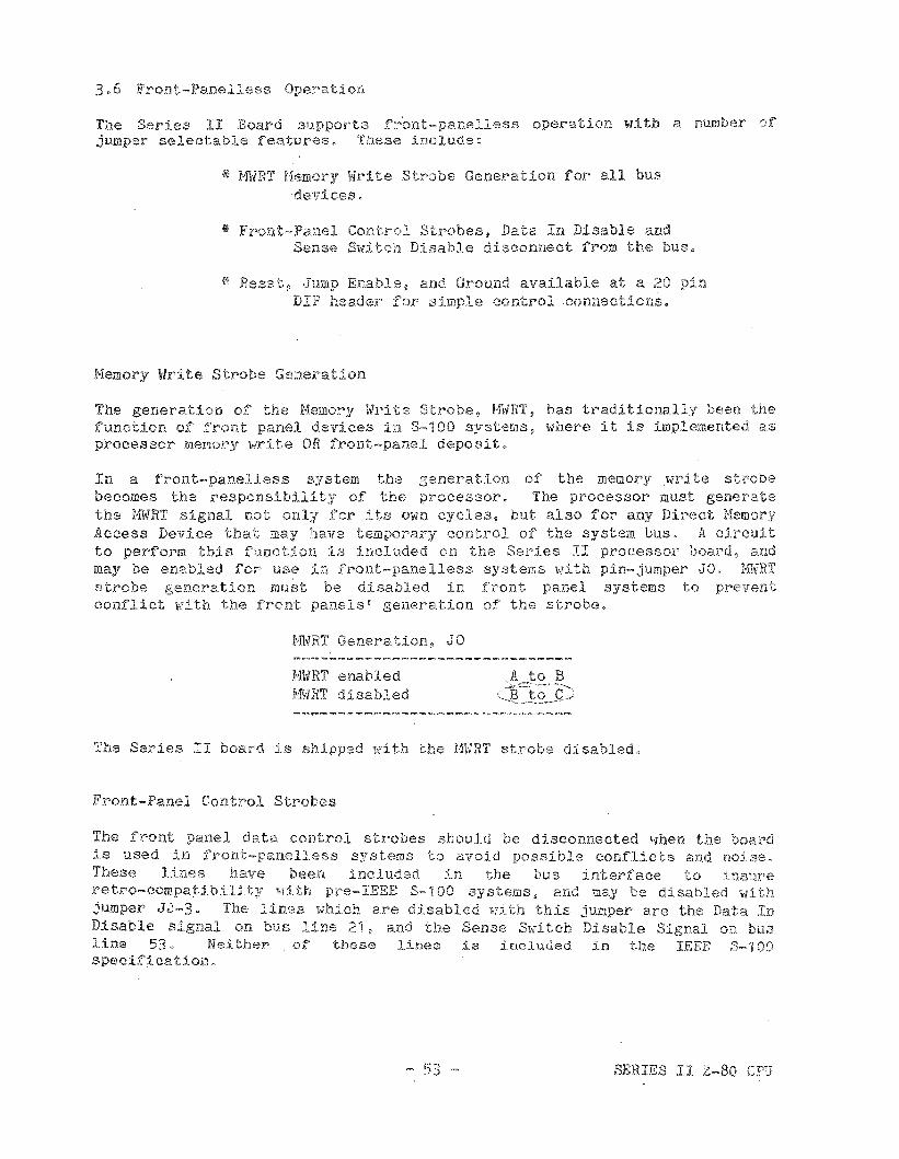
The Serles II Board s.upports f1l'ont-panelless operation Tilri th a number of'jumper seleotable features. These include:
* H\\1RT Hemmoy Write Strobe Generation for all busdev.tces.
• Front-Panel Control Strobes, Data In Disable andSense Switoh Disable disconnect from the bus.
~ Reset, Jump Enable, and Ground available at a 20 pinDIP header for simple controloonnections.
Memory Write Strobe Generation
The generation of the Hemory Write Strobe., HhmT, has traditiona11y bE)8n thefunction of front panel devices in S~·100 systems~ where it is implemented asprooessor memory Tt.rrite OR front-,panel deposito
In a front-panelless system the generation of the merJory .write strobebeoomes the respons.ibility of the twocessor. The prooessor must generatethe MWRT signal not only for' its own cycles, bu.t also for any Dil~ect l-lemoK'yAocess Device that may have temporary control of the system bus. A circuitto perform this function is included on the Series II processor board~ andmay be ena.bled. for use in fr'ont-panelless systems !!lith pin-jumper JO.strobe generation mu~t be disabled in front panel systems to preventconflict with the front panels' generation of the strobe.
tfWRT Generation, JO
l1t'l1RT enabledHllmT disabled
The Sel~les II board is shipped w.ith the t\HRT strobe disabled.
Front-Panel Control Strobes
The front panel data control strobes should be disconneoted when the boardis used 1n front-panel1ess systems to avoid possible conflicts and noise.These lines have been inoluded 1.n the bus interfaee to insureretro,;.,oompatibili tyl'IT.i th pre-IEEE 3-· WO systems 9 and may be disabled withjumper J,J,rn 3. The lin~,s 1\\ihich are disabled with this jumper are the Data InDisable signal on bUB line 2'~ and the Sense Switch Disable Signal on busline 53... Nei ther of these Ii-nes i-s included in the IEEE 3-100speciflcatic)lD.
SERIES II CPU
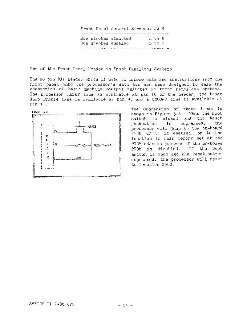
Front Panel Control Strobes$ JJ-3
Bus strobes disabledBus strobes enabled
A to BB to C
Use of the Front Panel Header in Front Panelless Systems
The 20 pin DIP header which is used to impose data and instructions from thefront panel onto the processor Ws data bus has been designed to ease theconnection of basic machine control switches in front panelless systems.The processor RESET line is available at pin '10 of the header ~ the ResetJump Enable 11.ne is available at pin 9, and a GROUND line is available atpin 11.
SERIES II Z-80 CPU
The Connection of these lines isshown in Figure 3-6. When the Bootswi teh is closed and the Resetpushbutton is depressed, theprocessor will jump to the on-boardPROH if it is enabled 1 or to thelocation in main f'ler:J.ory set at thePRm1 address jumpers if the on-boardPHON j.s disabled. If the Bootswitch is open and the Beset buttondepressed! the processor will resetto location 0000.
- 54 -
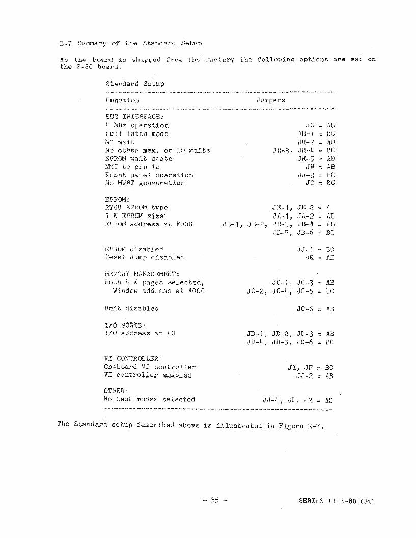
3.1 Summary of the Standard Setup
As the board is shipped from the'factory the following options are Bet onthe Z-80 board:
StandaK'd Setup
Function Jumpers
BUS INTEHFAGE~
~. MHz operation JG ::;; ABFull latch mode JH-l :: BeMl wait JH-2 ;::; ABNo other mem, or 10 ~Naits JH-,3 ~ JH-!.l ::;; BeEPROM wait state' JH-5 :::: ABNMI to pin 12 IN :::: ABF:t'ont panel operation J<J·~3 ;::; BCNo MWRT genenration ,JO ;;:: BC
EPROM:2708 EPROH type JE-l. JE-2 :::: A1 K EPROM size JA-1 ~ JA~·2 ;;:: ABEP1wH address at FOOD JB-I. JB-2, JB-3. JB-4 :::: A8
JB-5. JB-6 -, Be
EPROM dlsabled JJ-1 -- BeReset ,Jump disabled ,JK :::: AB
llLEHORY MANAGEMENT:Bot.h II K page.s .selected. JC··I. JC--3 ... AB
11\1ind01IJ address at AOOO JC-2, JC-4. JC-5 :::: Be
Unit d:l.sabled JC-6 - AB
I/O PORTS:I/O address at EO JD-l. JD-2. JD-3 :::: AB
JD--4. JD-5. JD-6 .. Be
VI CONTROLLER:On-board VI eon troller J1. JF' :::: BeITI controller enabled JJ-2 :::: AB
OTHER:No test modes selected JJ-4~ .JL. ,JH :::: AB
The Standard setup desoribed above is illustrated in Figure 3-7.
~ 55 ,- SERIES II Z-80 CPU
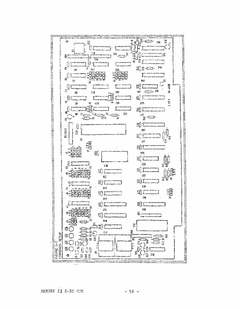
~o~om~
~O_O~;m;~!g
:§~o f.",.".,.m,,_.,.,~_~~
jm
i C::"':"'~.-~,.:J
~o ""'"--_.-1
'm~O~-=-'Ja...'),"""~"'''''''.,
Iii:!!
~Ol:",..",.,__m__.,l
;;:ii:\l gl>jjJ~-e:'.:}.,trn'I.
!~I
l!1'I!l?,~
@11l
.,.ml~
~O!i~
"'"...
SERIES II CPU
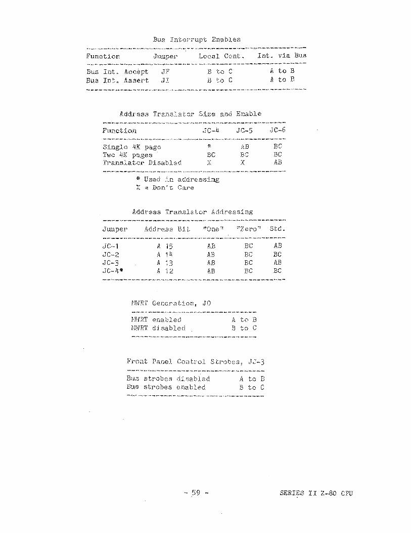
Bus Interrupt Enables
Function Jumper Local Cont. Int. via Bus
Bus Int. AoceptBus In t" Asstert
~TF
enB to CB to C
A to BA to B
Address Translator S12:,e and Enclble
Function
Single 4K pageTwo 4K pagesTranslator Disabled
JC_·1~
Bex
JC-5
ABBCX
eJC-6
BeBeAB
* Used in addre.ss:i.ngX :::; Donn t Ci':l.re
Address Translator Addressing
Jumper Address Bil;.
JC-1JC-2,JC-3.JC-4*
A 15A 1)~
A 13A 12
ABABA13AB
BeBeBCBe
ABBCABBe
Hll1RT Generation" ,JO
HIHlT enabledHtllRT disabled
A to BB to C
Front Panel Control Strobes" JJ-3
Bus strobes disabledBus strobes enabled
A to BB to C
- 59 - SERIES II 2-80 CPU

3.9 Ins talHng the Boar'd
Once you have selected the operating options ·for your processor board, yourna:>" install the board :tn your system. He reeoQIllend that, for initi21 checkout w you d:lsable th·(~ AddresiS Translator by setting <IC··6 to AB. If' yoursYfltern depends on bus intEH'JrLRpta usl-ng the S~1 00 s.i.gnals pINT and INTA, youshould consult section 3.4 of this manual regarding disabling theon-boardvectored interrupt controller.
With the systerr- power off p insert the board tnto the 03··100 bus, taking carenot to skeiN th(~ card flngers ",ri th respec t to the ed.ge connecto.r (1 t ispossible \l1.ith some card edge connector sockets to skew the board such thatthe gold fingers on the boar'd seat between the brushes of the socket).
Your processor board has been extensively tested before shipment from theInterSystem::> plant~ and. should. ,,<;.Tork the first time. If you neverthelessexperienoe difficulties~ here are some pointers~
Power down the system. DON'T remove any card irr~ediately; wait a minute forthe power supply· capacitor's to discharge. Check the fol1owing~
1) Is the board seated in the edge oonnector properly?
2) Has one of the chips on the board been Jarred loose in shipping?
3) How~ 8 your pO\'lier supply'? If the 118 volt Ii bus is less than '7volts~ this could be the problem.
4) Are the jumpers set properly?
If none of the above solva your problem, or if you need. any assistanceWhatsoever, give us a call at (607) 257-0190.
SERIES II Z-80 GPU - 60 -'
SecU.. on 4.0
Technical Reference Section
4.1 S-100 Not-to-be-Defined. Lines
lL2 Test lc10des
403 Board Timing Diagraos
- 61 - SERIES II 2-80 CPU
_.0 Technical Reference
This section of the user's manual describes our~'Not-t{)~be-Defined Llnes Ii on the S-" 100 bus~) overallrelat1onsh1pa~ and the basic board testing modes.
4.1 S-100 Not-to~be-Defined Lines (NDEFs)
use of theboard timing
The S-100 bus specification inoludes 3 lines which are oalledNot-to-be-Defined Lines f]:llDEFs.'. Ea,,'"h ~'laj'll'f"'c"'I' eo'" d t f th b\, .I .. ,. u.. " <CC.l.Ar-.r J[ pro uc s ,or _ e usmay use these lines p but must aSSure that they are not necessary for theproper operation of the product in a general S-100 system. As a generalpolicy w we at InterSystems "Jill not use the NDEF' lines for' any iineltJ1'I
function,39 but wIll include these lines as opti.ons on products where it :Lsfelt they provide increased compatibility with pre-standard products.
On the Ser:i8s II 2-,80 board, we have used the NDEF Une at Pin 21. all.traditional front panel devices, pin 21 IATas used as a data j.n di.sablesignal, allow'ing the front panel to impose data and instructions on tbeprocessor 9 s data bus. We inclU.de the DIDSE signal on the 20 pin DIP frontpanel eonnector~ but it is also available on th.e bus. depending on thesetting of Ule jumper' ~T.J~3. Connecting JJ-3 from A to B wEl enable theDIDSB signal from the 20 pin conneotor~ B to C 1,,rUl enable the DIDSB signalfrom NDEF LLne pin 21 >
In current InterSystems W DPS-·1 computer systems w tbe, DIDSB line is connectedbetvleen the front panel and the processor via. the bus line 2'1'1 and a 16~pin
cable connects to the front panel header. This impleoentation l.J'ill bephased out a:.9 mass~ten{j.:Lna ted 20,'"pin DIP cables becoo8 available inproduction quantities.
One other line has been included in the processor/bus interface for the sakeof retro-·compat1bilityo Thi::1 line l' form(~J~ly called Sense St~_itch Disable,!performs the same function as the Data In Disable line but is necessary tothe proper operati,on of II1SAI and. Al ta.:i.r front,=panels. Th.e SSioJDSB line (BusPin 53) has blsen assigned by the IEE~~ committee as a GROUND. If you havepurcha.sed a DPS··1 mai.pf'rame system 9 all data--:Ln--disa.ble functioDs "Jill bepE:rf'Orra8d by tl:'Hi') DIDSB line ~- e:l ther at pin 2'J I or on the 20,-pin DIP frontpanel connector.
SERIES II 2-80 CPU "~ 62 ,~
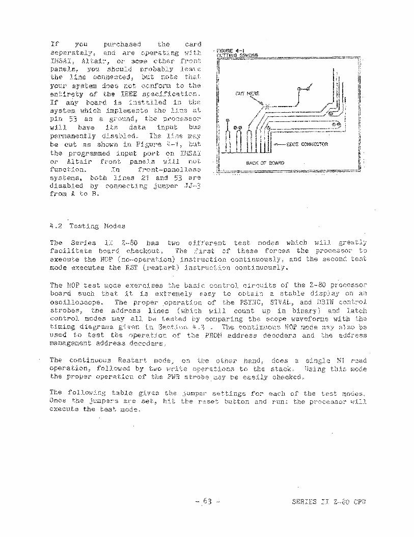
If you purchased the car'asepara.tely ~ and St'iS opera, t:ingIJ.1SAI p Al tair! or i.9,Ome other frontpanels, you should probably leavethe) line connected! bVlt JBote thatYOI.H'" !!l\ystem not OtOnfOl"'m to thl81ent.1rety of' the IE:EE s,pel~.:tficat1ol1.
If anJf board :iLs i in thesystem whioh implements the 11ne atpin 53 a[~ a , the proCeSsorwl11 have :it,g, da,ta btl:&.permsDent1~V dlsabled. The l:ine mii3-Ybe cu t as Sk"WHn in il~ _. 'I, bU.tthe programmt)d input por't on IH..SAIor Al talr front panels ",r notftmction. In front-,panellesssystems g both lines 21 and aredisabled by eonnecting jumper ,,1,3""'3from fA to Eo
4.2 Testtng Hodes
The Series II 2-80 has two different test Dodes which will greatlyfacili ta te board checkout. The f:Lrst of these forces the processorexecute the NOP (no-operation) instruotion continuously, and the second testmode executes the RST (restaR~t) 1.t:!struction continuously.
The NOP teat mode exercises the basic control circuits of the Z-BO processorboard such that it is l,~xtremE;ly easy to obtain a stable display on anoscil.loscope. The proper operation of the PSYlJC~ STVfAL~ and DBlNstrobes~ the address lines CfAihich \dll count up in binary) and 1acan trol modes may all h(") testE')d by eOJJlparing the scope wavefol:'ll1s with thet.imtne; diagrams l r,} 14 Th~ ~.oDti]::'\Jou;:, NOP TSlDoe !il3:v :'ll~"o beused to test the opeN'ttion of the. PROH address decoders and the addr'essmanagement address decoders.
The continuous Restart model, on the other hanet,oper'ation, followed by tl"ro !fll~ite operations to the,the proper operation of the PWR strobe.rnay be easi
does a single ~11 n;adstack~ Using this modechecked.
The fol1o~'lfi.ng table g:i,ves the ,jumper settings for each of the test modes,Once the jumpers are set, hit the reset buttOIDi and run, the processor Hillexecute the test mode"
.," 63 .." SEHIES II z~ GPO
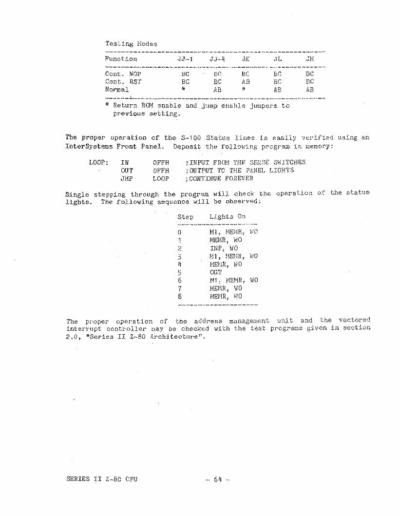
Test:lng Modes
Functlon JJ-1 J,J-4 JK JL JH
Cant. NOP Be Be Be Be BeCent. RST Be BC AD Be; BeNormal * AB ~ AB AB
* Return BOH enable and jump enable jut1pers toprevious setting.
The propsr operation of the S-100 Status linea is easily verified using anInterSystems Front Panel. Deposit the following program in memory:
LOOP: INOUTJHP
OFFHOFFHLOOP
; INPUT FROM THE SENSE SIUTCBES;OUTPUT TO THE PANEL LIGHTS;CONTINUE FOREVER
Single stepping through the program will check the operaUon of the statuslights. The following sequence will be observed:
Step Lights On
o M1~ MEMR~ WO1 MEMR~ ldO2 INP~ ~JO
3 M1 ~ HEt·1R ~ lrJO~ HEMR sl WO5 OUT6 M1~ MEMR~ WO7 HENRi HO8 HENRi \dO
The proper operation of the address management unit and the vectoredinterrupt controller may be checked with the test prog~~ams given in section2.0, "Series II Z-80 Architecture R •
SERIES II Z-80 CPU
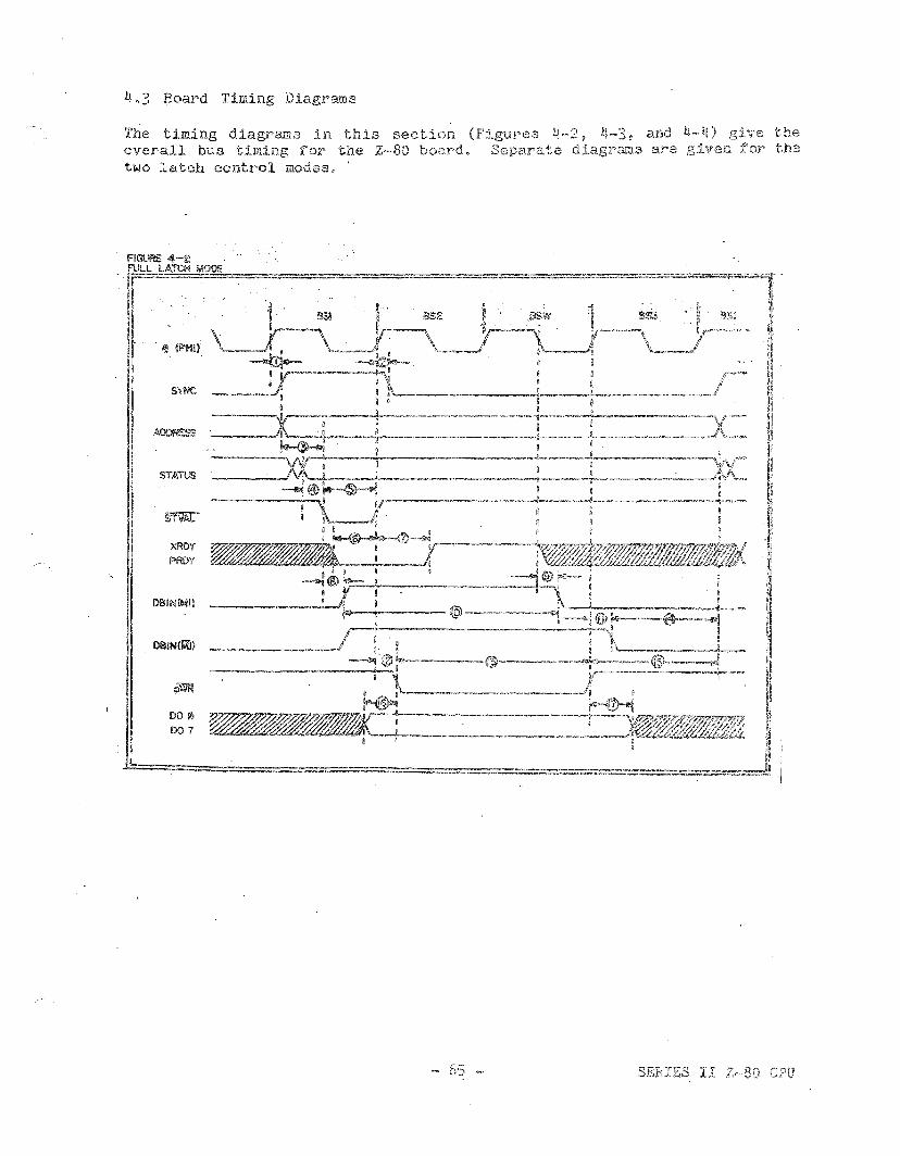
-4.3 Board Timing Diagrams
The timing diagrams in. this secth")n (F:1.gut-8S i~·~2 ~ ~ and 4- lt) gi.ve theoverall bus timing :for the Z-·80 boar'd. Separate cHagrams are g.iven :for thetwo latch control modes. "
STATUS
XRD'(
PRDY
OBIN(MI)
DO 0001
J..=.:===-- ...:=::........---...=. _
SERIES II Z- CPU

~-"~--"-i
iJ,r'IJlllllllJl11lTlll11!11l!llill"- IIWlfill.illlllfilIUJjJUilfll\,,_ I ~
IIr--~""~'"~'-_ ••_-~"'''''''-.'.'-1:'-'.'''=~''_.''.'--''-'._.'----····--·--11
1l'fI}.lli[ n
~_......:. .__._., ~r------\._--- __1._ ,_.._~." .._.._.__ IIi" . -4·~·"~ ..!
OON(fiill} . .. _.. _.J ~._-~- ...-~.-.-----.-----..-....
b=="""",,,,,,,,,==-,,,,==.,,,,,,,,,,,,,,,:=,,,,,,-=-=-=.=,-===- .::=""_==""'==""'.==""=-:..=-"~ _.....=-=.. ==
\i
UIi
~ ,,···_···_~· ..·__.._·_--·_·-IiI·
II~
". /_.. --\ '0
-'_II'~-_-I _.~_~__. .~
SERIES II 2-80 CPU - 66 -
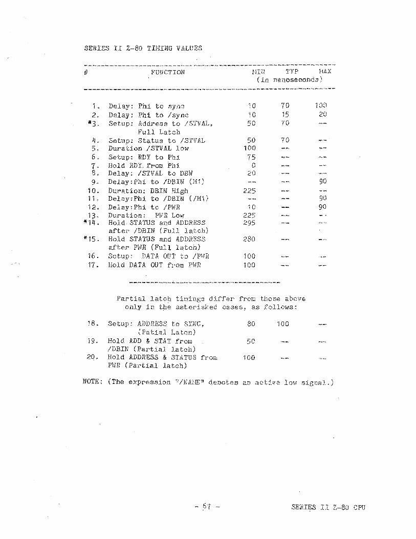
SERIES II .2-80 TINING VALUES
--~~---------~----~~---~--------~----~~-----~-~-----------~--:ff FUNCTION MIN TIP MAX
(In nat1oseconds)
L Delay~ Phi to sync 10 'fO
2. Delay: Phi to Isync 10 15*3. Setup: Address to ISTVAL~ 50 70
Full Latoh4. Setup: Status to /S'1''1AL 50 705. Duration /STVAL low 1006 . Setup: RDY to Phi 757. Hold RDY, from Phi. 08. Delay: /STiiAL to DBW 209. Delay:Ph::L to IDBIN (1011 )
10. Duration: DBnI High 22511- Delay~Phi to JDBIN (/Nl )12. Delay:Phi to /Pt'lR 1013. Duration: Pt'lR LoW' 225
if 111 • Hold STATUS and ADDRESS 295after /DBIN (Full latch)
*15. Hold STATUS and ADDRESS 280after Pt'JH (Full latcb)
16. Setup: DATA OUT to !PViR 10017. Hold DATA OUT from PWR 100
10020
90
go90
Partial latch timings differ from those aboveonly in the asterisked cases, as follows:
18. Setup: ADDRESS to SYNC~
(Patial La.tch)19. Hold ADD & STAT from
IDBIN (Partial latch)20. Hold ADDRESS & STATUS from
PWR (Partial latch)
80
50
100
100
NOTE: (The expression ~!/NJUJ.Elt qenotes an active 10111 signaL)
SERIES II Z-80 CPU

SERIES II Z-80 CPU - 68 -

Section 5
Parts' List' and Parts PlaceDent Diagram
- 69 - SERIES II 2-80 CPU
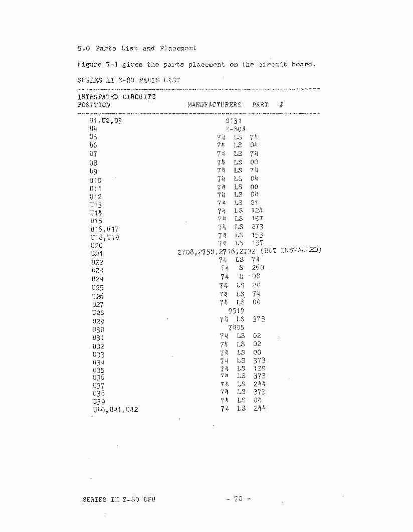
5.0 Parts L.ts t and Plaoei7.lent
Figure 5-1 gi'\i'es the parts placement on the cj.rcui.t board.
SERIES II Z··80 PA.Fl~rS LIS1~
INTEGRATED ClJitCUITSPOSITION .
SERIES II Z-80CPU
MANUFACTURERS PART ,
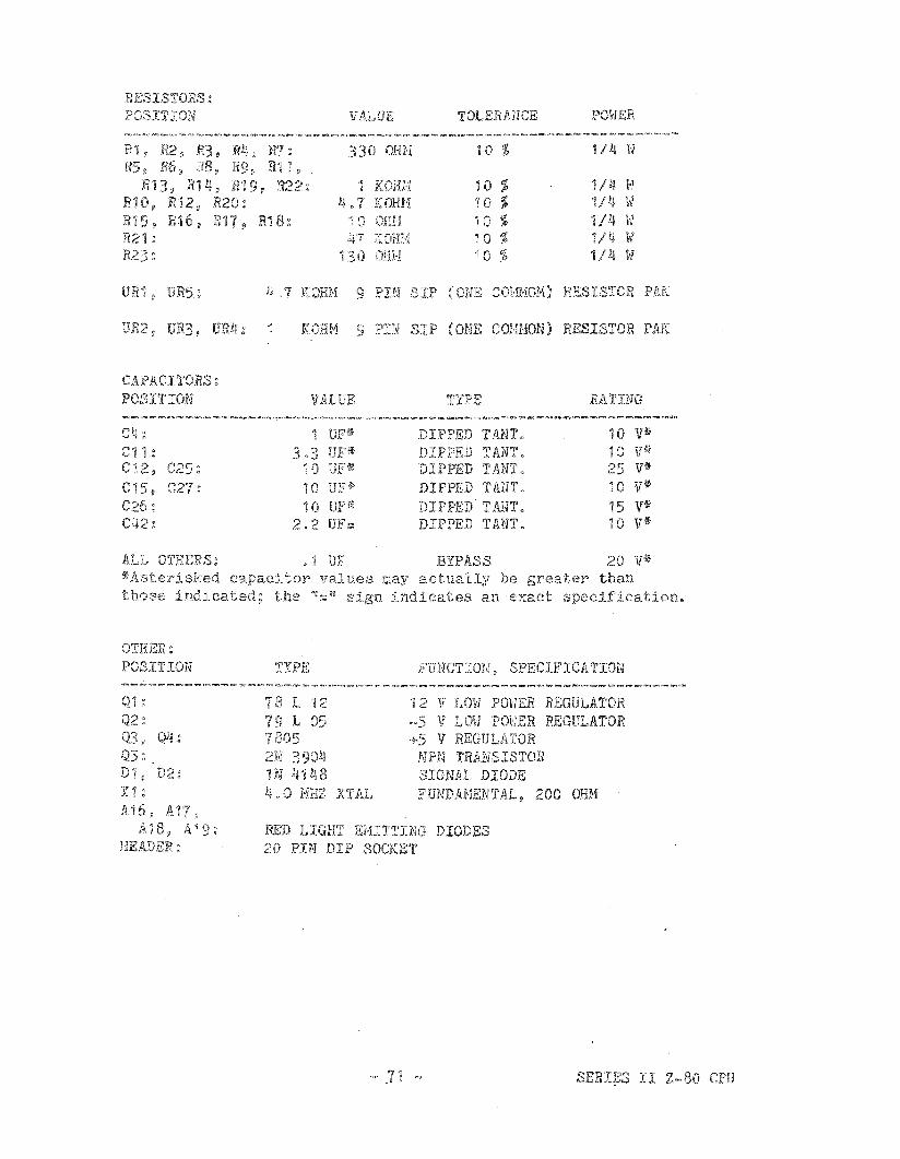
.RESISTORS~
POSITION TOLERAnCE POHER
HI R2 ~ lil3 ~ lil4 ~ 330 OHH 10 % 1/4 Hp FIG ~ RBI 1 S
3 p 4, 9w H22~ '1 KOHIl 10 % 1 ~!
.RW~ fll2 :1 R20~ ,I~ ,'7 KOHH 10 % 1 WR15 ~ rr16 ~ "f 9 B~ Hi OHH 10 % 1/kl I'JR2~;. 7 KOHH "! 0 % 1 t~
130 013J.I 10 % 1/4 Wl
URI it., 7 KOHH 9 PIN SIP ( COHHOH) RESISTOR PAK
VRZ ~ UR3~, KOBH 1) :PIN (ONE COHf.fON) HESISTOR PAR:
CAPACITORS~
POSITION VALUE TYPE RATING
CII ~; UF~ DIPPED TANT" 10 'Ill!!'Cll ; ""'ll ? Uf',1J; DIPPED TANT" 'lO v~'J "..J
C"/, ~2 ~ C25: 10 UF'i% DIPPED TANT" 25 'illY}
C15, C27: 10 UF,ll DIPPED TAlJT" 10 v*C26 ; 10 UP Ill, DIPPED TANT. 15 V',C!{2 : 2",2 UF\~ DIPPED TANTo 10 'It*ALL OTHERS: ,,'l HI" BYPASS 20 Viii*Asteriaked capacitor values Qay actually be greater thanthose indicated; the "_n sign indioates an exact specification.
OTHER:POSITION TYPE FUNCTION, SPECIFICATION
liED LIGHT EHITTING DIODES20 PIN DIP SOCKET
02:03;1 QJ-l:05 ;;DI,:n:A16 1 Al1~
iU8, A19:HEADER:
18 10 '~ 2
19 L Ol:'\j
'7I
2N 3HJ J.rj ,484"0 MHZ XTAL
'j.2 V P0I1ER REGULATORV POHER REGULATORV REGULJUOR
NPN T.RANSISTORSIGNAL DIODE!?UNDAHENTAL 9 200 OHH
SERI~S II 2-80 CPU
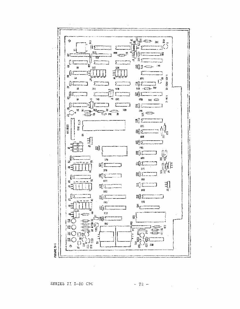
"'"iW:!m ~~lffi C;;l II
"'"
~,
@%'t1J ,'.fI.. !;-.-.---- t" !
.."
ffili:!l ,-c:::::J-, 2I1IM :i-!
~fi1l
~•
i1iO1l!1il~
aO";Iffi
~Omil'1l
~O...@~~
iWi'
:.:D ~,m,,",",",_,_,,_lj~,,~
iJII:""--,,",,,,,,~J),~ """.,l'J'>.i mtI <:iI"'!~(;:>. M
IlIf)
~ L':::=:::::::=::::==.:::::==~:::::::....-::::-...:=-..=::.:::::::::::::::=:::::::-..=:::::::=-.:....-=:::.-===:::===~-=====:::::::J
SERIES 11 Z-80 ,," 12 -

Section 6
Revisions and Manual Applicability
- 13 - SERIES II Z-80 CP
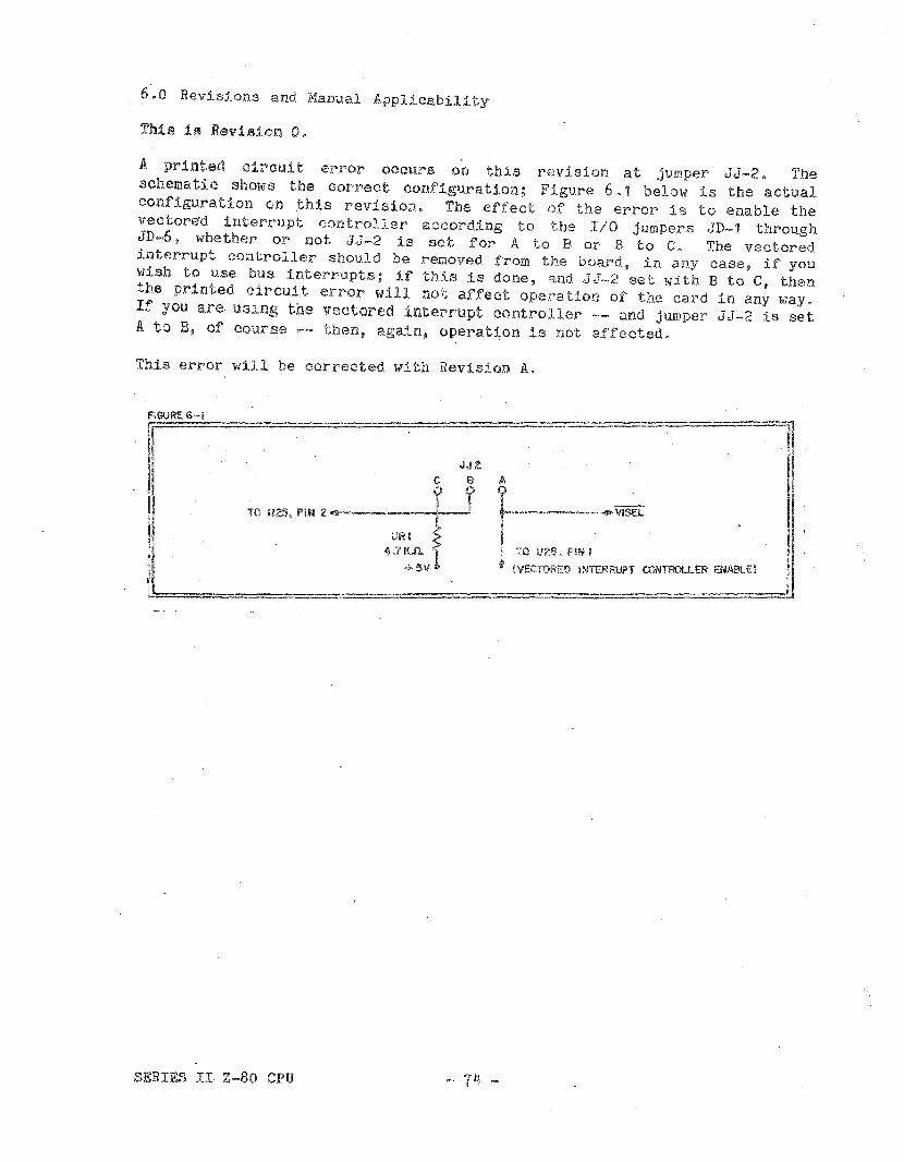
6.0 Revisions and Nanual Applicability
This 1s Revision O.
A printed C!ir(~uit error' occurs on this revision at jumper JJ-2. Theschematic show~1 the oorrect conf:J.guration; Figure 6.1 below is the actualconfigurat:1.on on .this revision.. The effect of the error is to enable thevectore-d interrupt controller according to the I/O jumpers JD-1 throughJD-6 ~ whether. or. not JJ-2 is set for A to 13 or B to Co The vectoredinterrupt controller should be reLIoved from the board~ in any case~ if youwish to use bus interrupts; if this j.B done~ and J<J.-2 set with B to C
tthen
the printed circuit error will not affect operation of the card in any way.If you are using the veotored interrupt controller -_ and jumper JJ-2 1s setA to 8, of course -- then, again, operation is not affected.
This error will be corrected with Revision A.
FiGURE 6-i
A
~-~-_ViSECI TO U28, P!i\11
~ (VEcrof~ED INTERRUPT a::lNTROLLER ENABLEl
-------_. - ..~.. ,..".
SERIES II Z-80 CPU

Section 7
Schematic Diagram
SERIES II Z-80 CPU

SERIES II Z~·80 CPU - 76 -

7\11 equi pw,n t manu f (1ctt~ reel by ITH1\C!, HJTEH,CjYS'l'Ei1S :':i hall be qUCl r anteec1against defects in materials and workmanship for 2 neriod of ninety (90)days from date of delivery to the Buyer by the Seller, ~nd the Seller agreesto repair or replace, at its sale option, any part which proves to bedefective and attributable to any defect in materials or workmanship.
SXCEPT FOR THE WA.RRANTIES TUl\~' 'J'HC GOODS l\RE f'lADE: IN A\',TORFI'1ANL IKE l\lII\HNER Z\;-1D IN ACCORDl\NCr. (HTH 'l'HF:SPECIFICATIONS SUPPLIED, SELLER MAKES NO WARRANTYEXPEESS OR Ir1PLIF.D, l\t1D Z\l',lY H1PLu:n \r,7J\RRI\N'I'Y OFrn:::PCIIl\;}'j' I\BILITY OR FI'J'IJESS tOR A Pl\RTICULZ\P PUrpOSE\'!HICH EXCEEDS TIlE FOREC::OH:G \JARRM?J'Y IS HERrmvD I EXLl\ITIED BY SELLER 7\ND EXCLUDED FP0l1 !\try l\GnEEflEWI'.
Buyer expressly waives its riqhts to any consequential damages,expense arising in connection with the use of or the inability to~oods for any purpose whatsoever.
loss oruse its
No warranty shall be applicable to any damages arising out of any act of theBuyer, his employees, agents, patrons or other persons.
In the event that a unit proves to be defective, an~ after authorization bySeller, the defective part and/or unit, as authorized, must be securelypackaged and returned Freight Prepaid by the Buyer to ITHACA INTERSYSTEMSfor repair. Upon receipt of the unit, ITHACA INTERSYSTEMS will repair orreplace, at its sole option, the defective part or product and return suchpart/product Freight Prepaid to the Buyer.
The remedies set forth herein are exclusive and the liability ofany contract or sale or anything done in connection therewith,contract, in tort, under any warranty, or otherwise, shall not,expressly provided herein, exceed the price of the equipmentwhich said liability is based.
Sellerwhether
exceptor part
toin
on
This warranty is given solely to the original Buyer. No employee orrepresentative of Seller is authorized to change this warranty in any way orgrant any other guaranty or warranty_
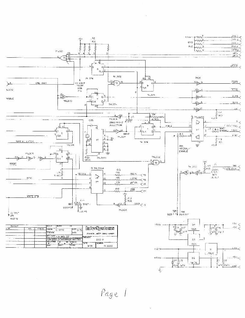
IS
+5V'o--o--,\N\;.6 . OMA 3 <5 .-9J'0-Z..(
UR3 t-'VVrv-7'--- -'O!!"M.0..J--(
11<[\ t-'VVrv-9'------ OMA 0 '8 -----·SXTR~
BUSINTERRUPTENABI.E
ABC00--
UR 3 ~~ ~I.&lL_./"I KO 60o-..£9.1{,ER F..1lJ.,--<:
A.J)j CNMI
SUITT
dF
c--------<e::------- :::~~"'6'-------- __ ._-',~.~<
140S
r=------------9"-jj)o!8L i'2~
74LS74
__-j . -.e'PHf!QI01~
14LS02
:~ 32 )-1"'3'- --+----'-"1
--_._------j.-----
74LS74
UR2IK[\
74LS74
t5V
1~8 II
74LSOO
74LS21
PARTIAL LATCH
f>"8'--- -'O"N~E'_·-"'W'!:A'l,IT'-__--l --.J V I CONTPAUSEU28PIS
.--==~2t::..-================= ------- XROY_____________~8~ 13 />-';';_--j-<!--.~-J----. -PRfiY-;::
!LSOO
----~-.----.----.---+_i--,;L
NA8LE
~==============.~_-=~_-=~~-------=---..-...----------------·=====t'=-='-·---=-=-~=~=-==-==-==-~-'=-=-='--=~=~~--=-~-~3~~~:r-=-J=G~~.llt-=-=-=-~~-+-~-c-""-----------~---1'-~-~"-;1--C23 741.S04 0-- .. +SV),
2MHZl4MHZ A C II f'--". 0W 1-"------.------"-(SELECTION 2 132MHZ"- ~ ~-MWRCTLOC.. 2MHZ (
37 . C B 3X~£ill-'=£~~
<I 17 --t I'INT--(
;; RI9
.::g? +5v1 I 1< fl.
SYNC
I~W"'",,'--
VI CONTWRU28 P2
REvISIONS SC~LE r~"T 0',I"T'ON O~H ""n'(:lY[O DRAWN [h]a<elJ~f1<LD[]OD£:lC. FRITZ IDATE 8/79
CHECKED IDATE ITHACA ~ ~tW '10!H( 14moo
D€SIGNED K. ELMQUISTPROJECT
UNLESS OTHERWISE NOTED loBO IIF,±ACtIONS L..OO •. IXX'I lA~GLES
DATE INUMeEfIRAOli IOOAFT IFINISH 9/79 IA-2000
INT NMIU28P17. U4PI7
+Sv0---_--..----<>---1
+12Vo- ----.-...,.-----+----1
J~II _C12
:_I-'---"--_~I--- ___J,-'D~3errl "-"JJ2..<
/\ '"/"([9 ."~
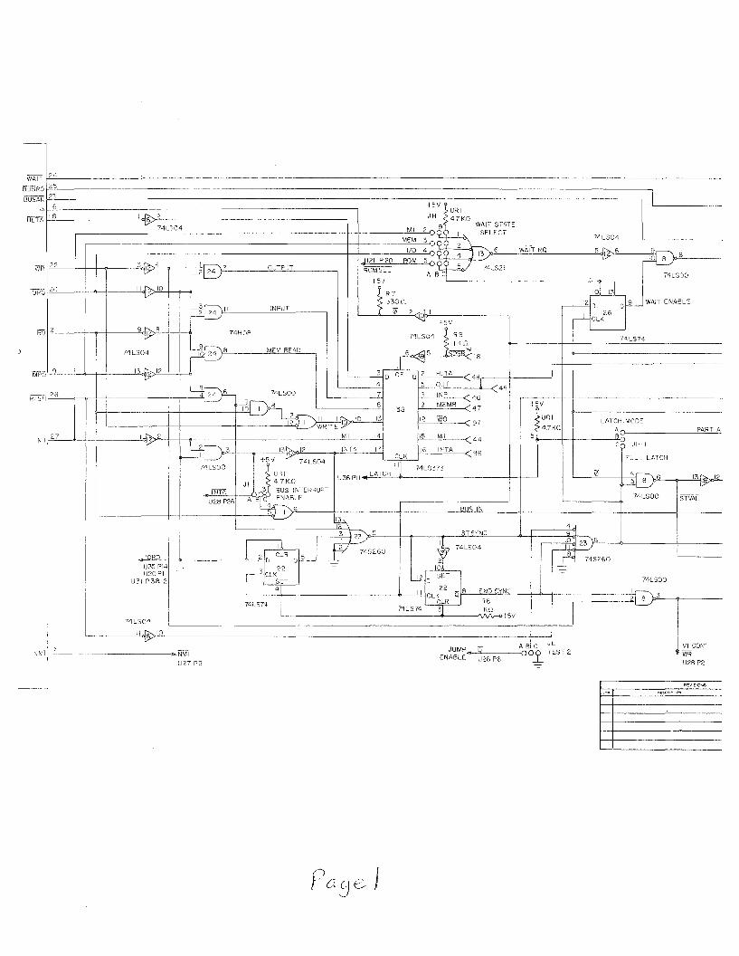
II I' 10
I 32 24
13I'12 2.4
INPUTQ 9 WAIT ENABL.E
RD -?L....- --j--or-',--- 91l!Y""~8__ " ,
74L5049 8IC 24
74H08
___,. MEM READ --,
74LS04 74L574
13 I" ,,1-2-,-, 1
PARTI AI
- ---- -- ---".-l-------
URI
4.7KCl
,- +5V -- - ~ _
LATCH MODE
~O>---------5l>-_-+-1~__ CC:;:;,-' J H-I
FULL LATCH
Ml 27
741.500
REVISIONS
VI CaNTWRU28 P2
...--' ... NMI
U27 P3
74L50
4
JQ....~====================---------~~;~~~~~=~A~B~.I~Ct ~~~5T 2
JUMP..,>--"()-:-::-::-::, 001. _
,______ 11"""6 10 _
'V'" ENABLE U26 P6
L
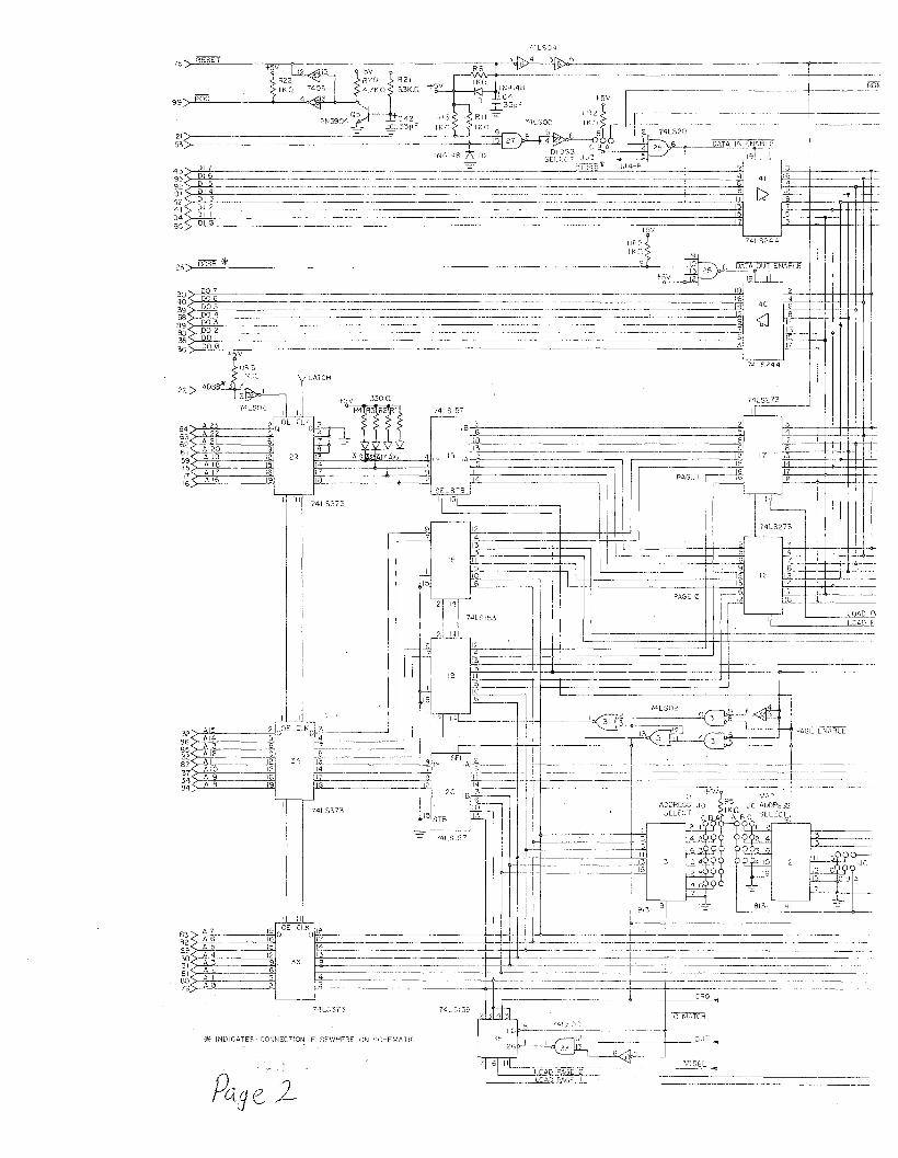
LOAD p,···L~)A\D~
14i2
1816
2'5
PAGE I
_v~~
l"lT- r-'I.~1CH
-_Q~
__!')RO 1
69'
--'2
--_.--------
G....--:l1..5
74LSO()
I~~.74LSn2 9._,6-..",o;r;1;___.~_.~ IO~~
~" 12. 4~~1PAGEE'NABlE___.- -. 31 II_~------J !i
-_.__ ......_. .__~~~:. "1-----+
-- LOAD PAGE 0 ---
~~. PAGE ..~_.-======--=.~=~--===-. __._
,l41..S,],:j
~~=---===:--- I R(jiR6
18
19
20
l41_5157
151ST8
R21 +5v I I,K? I~C4- +~5V! ~ __ ~:'0KfC ~:;3Pf IJR2 ~__ -~-c
.I. II\fl [' 2 74LS20 -i\ IN ~NABL"" ~ ,," '~" , "" --""'--- ",[,Wn~9R ; f ._ A 4 2~ _- '7 4.B._ 5 2'+= ' """"" ,i"T .IJ JJ~-B- - Dc ',FI ',11)5.8. _" '~..__ ~ .__ ~~- --=c -c.-=c"CC: . ..- " t> fJ-L:tiUJ.I~ ----~- -. -. -' 13 i±:=
- -'----='~=- '-,:;- I .._- l~~i 3
~-_'!.
11_7
'
~--._---------._---
.--~J
181";1-- ---._..
~13------ -'--8--- .. --.
I4
~
74LS373
74L.S373
36
Pa,ge 2-
-;:\( INDICATES CONNECTiON EL.SEWHERE ON SCHEMATIC
'AD~ 122~ ~
23) DOSS"" ~ .- .- ---- ---- -- --._ -- 40 Uift~-- --- -_.. ---- <J I~
QQ..L....... --.:::=:=---=-------- --- '-. 'I~ +-+~ ..----.-.--.---- ..-... .-.. ---.--- 3l i~1i I
- -_... ---..•• - ... - ---- ----.- .-- -- --i4LS244 II
75~:eff
;~S===~========-' -~- ...
99) roc
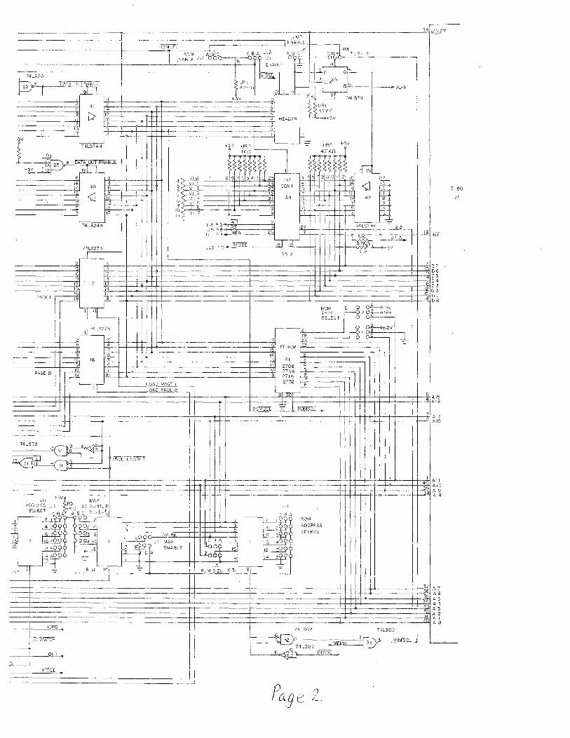
74LS02
------
z- 80
U4