it built-in-test verification techniques i
TRANSCRIPT

RADC-TR-86-241,Final Technical Report
00 February 1987
• It
BUILT-IN-TEST VERIFICATION TECHNIQUES i"
Boeing Aerospace Company
Jeffrey H. Albert. Mike J. Partridge and Richard J. Spillman
IAPPROVED FOR PUBLIC RELEWSE, DISTRIBUTION UNLIMITED
DTICS ELECJOL 1 6 1987
ROME AIR DEVELOPMENT CENTER G--Air Force Systems Command
Griffiss Air Force Base, NY 13441-5700
-, . A A..... . .., . , -.-.. ... ....•..... .,.... ... .. '. --- ,".. , . . -:: : :: : : : ... . . . . . . . .

%J'p
This report has been reviewed by the RADC Public Affairs Offica (PA) andis releasable to the National Technical Information Service (NTIS). At NTISit will be releasable to the general public, including foreign nations.
RADC-TR-86-241 has been reviewed and is upproved for publication.
APPROVED:
THOMAS L. FENNELLProject Engineer
APPROV 3D:
W. S. TUTHILL, Colonel, USAFDirEctor of Reliability & Compatibility
FOR fliE COMMANDER: ~~ M
JOHN A. RITZ
Directorate of Plans & Programs
If your address has changed or if you wish to be removed from the RADC mailinglist, or If the addressee is no longer erplcyed by your organization, pleasenotify RADC (RBER) Griffiss APB NY 13441-5700. This will assist us inmaintaining a current mailing list.
Do not return copies of this report unless contractual obligations or notices
on a specific document requires that it be returtied.SN
J.
.4.11
Ž.:-. .

REPORT DOCUMENTATION PAGE OAh9NsL Ohu4-Q180In. REPORT SECURITYV CLASSIFICATION 1b. RESTRICTIVE MARKINGS
UNCLA.SSIFIED N/A2*. SECURITY CLASSIFICATION AUTHORITY 3. DISTRIBUTIONIAVAILAUILITY Of REPORTN/A Approved for public release; distributionZ.DICLASSIFICATION / DOWNGRADING SCHEDULE unlimited.
4. PERFORMING ORGANIZATION REPORT NUMIERt(S) S. MONITORING ORGANIZATION REPORT NUMBER(S)
N/A RADC-TR-86-24111a. NAME OP PERFORMING OReCANIZATION 6b. OFFICE SYMBOL 7a. NAME Of MONITORING ORGANIZATIONBoeing Aerospace Company (faliw) Rome Air Development Center (RBER)
&L DDRSS ft tft = W C*) b, ADDRESS (Clay. Statt. adZIP Code)P. 0. Box 3999 Griffiss AFB NY 13441-5700
Seattle WA 98124ft. NAME OF FUNDING/MPN'SORING 8 b. OFFICE SYMBOL 9. PROCUREMENT INSTRUMENT IDENTIFICATION NUMBER
ORGANIZATION (If( appl*cabl)Rome Air Developavent Center RBE F.30602-84-C-0021
kc ADDRESS (Cfty. Stat*. .td ZIP Cock) 11.S-PEO FUNDING NUMBERSP4RM PROJECT TASK IWORK UNIT
Griffiss AFB NY 13441-5 700 ELE MENT No NO. NO. CCESSION NO.i,2702F 2338 02 r 1.
I1. TITLE (kcftx*:9ecur#.) Ctslawcetion)£UILT-IN-TEST I'MIIFICATI0N TECHNIQUES
12. PERSONAL AUT4O-R(S)Jeffrey H. Albert, Mike J. Partrtdae. Rihr ilumRaghAsnsr-n
13a.TYP OFPEPFIT11.b. TIME COVERED f14.D'AalE OF REPORT (YWr,41100t.Day) 115. PAGCON
16. SUPPLEMENTARY NOTATIONN/A
17. FED COSATI CODE~i 1t. SUBJECT TERMS (Continue on revwne it necessary and idanftl, by block numbed)GRUIEBGRU Built-In-Test1 / Built-In-Test Ver .ication,)
05 IT rIf~ni Slmular~io
S19. ABSTRACT (Continue on rev'rmse if nwesueny and ednirwyb block number)This report documentsB the effort to develop practical Verification methodol ies for theaccurate and economical test and demonstration of Built-Ir-Test (BIT) subsystems andcircuitry. These methodologies are to be applicable to both formal verification of asystem for demonstration of BIT effectiveness (test system verification), and underoperational conditions, to verify that the BIT is functioning as designed (test systemcondition assessment).
Currently BIT is verified by Rnalysis of the design or by demonstration of a limited setof simulated faults. Verification of BIT capability by design analysis for verificationpurposes is not currently recognized as a reliable means of veri~ficatioun. Use of simulatedset of faults has also proven to have low effectiveness for evaluation of BIT capabilities,as veil as being costly. BIT on equipment in the field can selý'om be tested to discoverfailures in the BIT circuitry, which results in gradual degradation of BIT effectiveness.
20. DISTRIBUTION /AVAILABILITY OF ABSTRACT 21. ABSTRACT SECURITY CLASSIFICATION(3 UNCLASSIF:ED/UNL!MITED 01 SAME AS RPT. Qj DTIC USERS UNCLASSIFIED
22a. NAME OF RESPONSIBLE INDIVIDUAL I22b. TELEPHONE (include Area Code) 22. OFF!CE SYMBOLThomas L. Fennell I (315)'330-3476 RADC (RBER)DD Form 1471, JUN 86 Prev~ious editions are obsolete. SECURITY CLASSIFICATION OF THIS PAGE
UNCLASSIFIED

PREFACE
This report documents the results of the effort for the
Rome Air Development Center Contract F30602-84-C-0021, BIT
Verification Techniques.
The work was accomplished by the Engineering Technology
Organization of Boeinq Aerospace Company under the
management of T. A. Nicolino, with support provided by
Dr. Richard Spillman of Sp.,llman Research Associates. Theprincipal investigators were Mike Partridge andsubsequently Jeffrey Albert.
The contract was administered by the Rome Air DevelopmentCenter. Technical and administrative support was provided
by Thomas eennell. Management was provided by Jerome Klion(RADC/RBET).
Q- -. P
i

TABLE OF COHTENTS
1.0 Introduction 1-1
1.1 Background 1-1
1.2 Objective 1-2
1.3 Program Plan 1-3
'1.4 Report Organization 1-5
2.0 Military Electronic Design Trends 2-1
22.1 Design Technology Trends 2-1
2.1.1 Computer-Aided Engineering 2-3
2.1.2 Artificial Intelligence 2-5
2.1.3 Modular Avionics Packaging 2-7
2.1.4 Pave Pilla.r 2-9
2.1.5 Integrated Diagnostics 2-11
2.1z6 Architectures 2-13
2.1.7 Data Buses 2-15
2.2 Component Technology Trends 2-15
2.2.1 Driving Forces 2-16
2.2.2 Component Parameters 2-18
2.2.3 Trends 2-20
2.2.4 Trend Summary 2-26
2.3 VHSIC Technology 2-26
2.4 Impact on BIT Design 2-28
3.0 TSV/TSCA Techniques 3-1
3.1 TSV Techniques 3-2
3.1.1 Figures of Merit 3-4
3.1.2 Failure Modes and EffectsAnalysis 3-5
ii

3.1.3 8imulation 3-S
3.1.4 Statistical 3-10
3.2 TSCA Techniques 3-19
3.2.1 Fault Insertion 3-19
3.2.2 Self-Checking Checkers 3-20
3.2.3 Other Teohniques 3-23
4.0 TSV/TSCA Improvements Invwbstigationa 4-1
4.1 TSV Techniques 4-1
4.1.1 Nov Figures of Merit 4-1
4.1.2 Test Repetition Metý•ods 4-6
4.1.3 Extensions of FMEA 4-9
4.1.4 Advanced Simulations 4-9
4.2 TSC7h Techniques 4-14
4.2.1 Overlapping BIT 4-14
4.2.2 Fuzzy Pattern Recognition 4-15Applications
4.2.3 Fault Insertion 4-15
5.0 TSV/T&$CA Evaluation and Selection 5-1
5,1 Rejected Techniques 5-1
5.2 Evaluation Criteria 5-3
5.3 Evaluation 5-6
6.0 TSV Improvement Details and Specifications 6-1
6.1 Methodology 6-2
6.2 Architectural Simulation Test Case 6-4
6.2.1 Example System and Model 6-6
6.2.2 Built-In Test Description 6-8
6.2.3 Fault Model Description 6-10
iii

6.3.4 Simulation Software Nodel 6-12
Description
6.2.5 Results 6-15
6.3 Key issues in Using Behavioral 6-17Fault Simulation to Verity BITCoverage
6.4 Architectural TAvel Simulation for 6-23TSV: Specification for FurtherDevelopment
6.4.1 Objective 6-23
6.4.2 Scope 6-23
6.4.3 Baokground 6-24
6.4.4 Tasks/Technical Requirements 6-25
6.5 Epecification for Utilization of 6-27Architectural Level Simulation forTest System Verification
6.5.1 Scope 6-27
6.5.2 Requiremeats 6-27
7.0 TSCA Improvement Details and Specifications 7-1
7.1 Overlapping BIT 7-1
7.1.1 Ovezlapping BIT Concept andStructure 7-2
7.1.2 Overlapping B:T InterpreterCircuit 7-2
7.1.3 Application of Overlapping BIT 7-7
7.1.4 Overlapping BIT Specification 7-24
7.2 Fault Insertion for TSCA 7-33
7.2.1 Fault Insertion Implementation 7-34
7.2.2 Fault Insertion Design Issues 7-38
7.2.3 Fault Insertion Output Ptocessing 7-40
7.2.4 A New Fault Insertion Device 7-44
iv

7.3 TACk Guidelines 7-46
SO Cono18asiws S-i
Rferenoes Rm-1
ibl/ography as-i
Appenidb At Aiseit.nent of V8ITC Built-In Test A-1
Appendix a: Naming Codes 3-1
V

LIST OF FIGURES
Figure 1-1 BIT Verification Program Task Flow 1-4
Figure 2-1 Military 3lectronics Design Trends 2-2
Figure 2-2 Avionics System Architectures 2-11,
Figure 2-3 Device Trends 2-2 1.
Figure 2-4 Speed of Semiconductor Memory 2-23
Figure 2-5 16-BIT Computer Capabilities (CHIP) 2-24
Figure 2-6 Semiconductor Speed - Power Performance 2-26
Figure 3-1 BIT Verification Methods 3-3
Fiqure 3-2 FMEA - Derivad BIT Analysis 3-7
Figure 3-3 FNECA Steps with BIT Evaluation 3-9
Figure 3-4 Effect of Reliability on BIT Performance 3-14
Figure 3-5 State Diagram and Transition Matrix for BITOperation Model 3-17
Figure 3-6 Forced Failure Mechanism 3-21
Vigure 4-1 State Diagram and Transition Matrix forExample of Modified Gleason FOM 4-5
Figure 4-2 Simulation Testbed Incorporating HardwareElemente 4-11
Figure 4-3 General Levels of Simulation 4-13
Figure 6-1 Design/Analysit Flow for Simulation use in TSV 6-5
Figure 7-1 Overlapping BIT Structure 7-3
Figure 7-2 Overlapping BIT Interpreter CircuitBlock Diagram 7-5
Figure 7-3 Count System 7-6
Figure 7-4 BIT Evaluator 7-8
F'.gure 7-5 State Diagram for the Failure Detector 7-9
Figure 7-6 State Assignment and State Table 7-10
Figure 7-7 State Map 7--11
vi

Figure 7-S Failure Detector State Control Logic Diagram 7-12
Figure 7-9 Final Check Logic 7-13
Figure 7-10 Control system Logic Diagram 7-14
Figure 7-11 State Assignment 7-15
Figure 7-12 Naps for Nsxt state Decoder 7-16
Figure 7-13 Four Line Dus Example 7-19
Figure 7-14 Overlapping Nanming Code Applied to an8-SIT Word 7-22
Figure 7-15 Standard. System 7-25
Figure 7-16 Standard Overlapping BIT Structure 7-25
Figure 7-17 Cases where multiple Failures Yield aBIT Stream Identical to Single SubsystemFailure 7-29
Figure 7-18 Case where multiple Failures Yielda BIT Stream Identical to Single BITSegment Failure 7-29
Figure 7-19 Fault Insertion System Block Diagram 7-36
Figure 7-20 Fault Insertion Control System 7-37State Diagram
Figure 7-21 Circuit for a Fault Insertion Device "-45
Figure 7-22 Sample Uses of Fault Devices 7-47
vii

LIST OF TABLES
Table 1-1 Report Organisation 1-6
-Table 2-1 Digital Funotions in Military Electronic 2-17Systeas
Table 3-2 Expected Growt•h in Digital Throughput 2-17Requirements for Various Defense Systems
Table 4-1 Possible RIT Verification Techniques 4-2
Table 5-1 Evaluation Criteria 5-4
Table 5-2 Options Remaining After Initial Filtering 5-7
Table 5-3 Test System Verification Evaluation 5-8 - 5-9
Table 5-4 Test Systea Condition Assessment 5-10 - 5-11Evaluation
Table 6-1 BIT Coverage Predictions 6-16
Table 6-2 BIT Coverage Coupariion: Simalatiorn 6-18Results vs Predicted VTalues
Table 6-3 Issues and Improvement Areas 6-19
Table 7-1 Failure Rates and Probabilities for 7-32Overlappin•g BIT Example
Table 7-2 Relative Coo~t of Output Haecmi•ims "/-41
viii

SUMOARY
This report documents the results of a two your effort to
develop techniques for Built-In Test (BIT) verification. The
objective of the contract was to develop specifications and
technical details for practical verification methodologies
for the accurate and economical test and demonstration of
built-in teot. This inclu4ed koth Test System Verification
(TSV), to verify that BIT is dtsigned to meot its performance
requirementsl, and Test System Cendition Assessment (TSCA), to
verify during operation that BIT is performing as designed.
Current test system verification methodologies have proven tobe inadequate and costly for effective evaluation of BITcapability. As q consequence, these fa=tors have contributedto questionable BIT peyformance in the field.
This contract has addressed potential improvements in TSVtechniques, to provide the designer with better toole todesign and integrate BIT into a system. It has alsoaddressed development of TSCA techniques, to provide
assurance to operators and maintenance personnel that the BIT
is operating correctly.
Task 1 investigated current military electronic designtechnology and projected trends for the near future todetermine their impact on BIT design. The following designtrends were examined to determine their impact on BIT design:
Computer-Aided EngineeringArtificial Intelligence
Modular Avionics PackagingPave PillarIntegrated DiagnosticsArchitecturesData Buses
ix
General trends in electronic component technology were alsoexamined, with particular emphasis on Very High SpeedIntegrated Circuits (VHSIC). The conclusions of this taskwere that no radical changes in technology would occur before1990, and that the current trends toward increased integratedcircuit functiona .Jy and increased performance wouldcontinue. As integrated circuit technology advances resultin increased performance capabilities, the requirement foradvanced BIT design at the integrated circuit level shouldresult in more effective BIT. One possible result cnuld bedevelopment of BIT chip sets incorporating some smart BITconcepts.
Task 2 surveyed current and proposed TSV/TSCA techniques byrevieving literature and making personal contacts inindustry, military and academia. The following techniqueswere identified:
TEST SYSTEM VERIFICATION
Figures of MeritFailure Xodes and Effects AnalysisSimulationStatistical
TEST SYSTEM CONDITION .SSESSMENT
Self-Chocking CircuitsFault Insertion
Descriptions of these techniques were prepared and areincluded in the report. Within each of these categories,specific implementations are numerous P'nd vary greatly. Thisindicates a need for standardized effective verificationtechniques.
In Task j, potential improvements to the techniquesidentified in Task 2 were investigated. TSV improvementsassessel included candidates for new figures of merit, use of
x

test repetition methods for assessing intermittent faults,
extensions to failure modes and effects analysis methods and
advanced simulation concepts. The investigation of TSCA
improvements led to the development of a new concept,Overlapping BIT, which is described in section 7.1.
Task 4 consisted of the evaluation of techniques and
potential improvements. An initial filter screened out
techniques that did not meet the requirements of being
practical, economical and accurate. The primary reasons for
elimination at this stage were very limited applicability or
high complexity. The remaining techniques were evaluated
against several criteria, some of which were qualitative and
some which were quantitative. The evaluation resulted in
three techniques being selected as the most promising
candidates for improvement. These were behavioral simulation
for TSV, and overlapping BIT and fault insertion for TSCA.
Task 5 involved further development of the techniques
selected during the evaluation task. Behavioral level
simulation was developed for TSV, with overlapping BIT and
fault insertion developed for TSCA. After this additional
development, these techniques continued to show promise for
developing into effective verification capabilities.
Investigation into the use of behavLoral level simulation for
TSV led to the conclusion that the technique shows promise
but is not ready today. Improvements in simulation software
and in fault modeling, plus increased availabilty of powerful
computers, will be necessary before simulation use for TSV in
complex, modern systems can be practical on a fairly
universal basis. Most of the necessary improvements will
evolve naturally over the next 3-5 years, but some stimulus
is necessary in the areas of concurrent fault simulation and
the relationship of functional fault models to physical
xt

faults. A specification for recommended futher development
in -this area was written as part of Task 5.
The TSCA techniques, overlapping BIT and fault insertion, are
applicable in their currant form now. For each technique, a
control system architecture was developed, and requirements
and limitations were identified. For overlapping BIT,
several applications (to data buses, memories, analog
interfaces and Hamming code extensions) were identified and
explored and a specification for its use was developed. For
fault insertion, a new device to insert faults was developed.
This device uses less hardware and permits inisert ion of a
greater variety of faults than other devices found in the
literature. A number of fault insertion output processing
concepts were documented, along with their relative strengths
in different application contexts. Also, since overlapping
BIT and fault insertion are applicable in different
situations and they have different strengths and weaknesses,
guidelines for their use were developed.
An additional noteworthy finding of this study was that
agreement on standardization of methodologies is at least as
necessary as finding better techniques. Standardization
would eliminate use of the ad hoc methods frequently used now
and would make it unnecessary to spend time selecting a
method for each new program. It would also result in the
application of BIT verification methods being better
understood and accepted by users. Promoting user acceptance
of integrated approaches to BIT would be in itself a
significant achievement.
xii

1.0 INTRODUCTION
This report documents the results of a two year effort todevelop practical, effectivi methodologies to verify thatBuilt-In Test (BIT) designs meet their requirements (test
system verification) and, in operation, perform asdesigned (test syatem condition assessment).
1.1 BACKGROUND
Maintenance of weapon systems is becoming an increasinglyimportant consideration in weapon system development.
Improvement in the maintenance capability of a weaponsystem greatly reduces the total life cycle cost of the
system since the cost of maintenance is a significantportion of that cost. Improved maintenance also increases
availability which, in turn, reduces ýhe nurber of systemsthat need t6 be acquired, lowering the acquisition cost of
the weapon system.
With the implementation of MIL-STD-2165, TestabilityProgram for Electronics Systems and Equipments, it will
become essential to have the tools to predict and measurethe various testability requirements. This standard
specifies a program to incorporate testability disciplines
into programs from concept exploration phase throughproduction and deployment. Elements from the system level
to the integrated circuit component level are affected.
Key to successful applicaticn of this standard is
specification, prediction, measurement and verification of
the testability evaluation parameters (e.g., fault
detection rate, fault isolation rate and false alarm
rate). Experience has shown that adequate verification
1-1

technique. for these parameters do not currently exist.
Nowv technique. will likely use computer-aided tools for
verification and assessment methodology application. This
would provide standardized, accurate verification at lower
coat and make verification techniques available to design.engineers at all phases of development.
Numerous techniques have been used for verification of
BIT systems. These include manual analysis, c~omputer
analysis by modeling and simulated fault insertion,
simulated fault insertion in actual hardware and use of
real faults by collecting faulty components. Each of these
technique. has differing costs associated with their use
and the effectiveness of each varies. In general, the
greater the cost, the greater the effectiveness. The BIT
performance in the field-has not,, however,, been as good as
the verification techniques have predicted.
Advanices in electronic design technology and new BIT
developments will place additional burdens on the
verification process. In particular, advances in VeryLarge Scale Integrated (VLSI) circuit technology present
special BIT verification problems. In VLSI devices there
are more locations where failures can occur (e.g. due to
increased gate count),~ there are additional failure modes,
and the circuit description and failure mechanisms are
often not known to the subsystesm and system designers.
1.2 OBJECTIVE
The objective of the BIT Verification Techniques effort
is to develop the specifications and technical details
for practical verification methodologies for the accurate
and economical test and demonstration of built-in test.
This applies both to Test System Verification (TSV), to
1-2

verify that BIT is designed to meet its performance
requirements, and Test System Condition Assessment (TSCA),
to verify during operation that BIT is performing as
designed.
The methods selected for development must be practical in
that they are generally applicable to a wide range of
t-lectronic and BIT system designs and usable by the
majority of industry and military users without substantial
capital investment. They must verify parameters that are
definable in a procurement specification. They must also
be accurate so that the verification results reflect whatis expected in operation. Finally, the techniques mustbe economical to use and not require investments inadvanced computers and simulation capability beyond the
means of most companies.
1.3 PROGRAM PLAN
The BIT Verification Techniques program is structuredaround five tasks as illustrated in figure 1-1.
Task 1 identified near-term trends in military electronicsdesign technology and investigated their impact on BIT
verification. The trends were used to determine whereimprovements are needed.
In parallel, task 2 surveyed literature as well asgovernment, industry and educatioral sources to identify
TSV and TSCA techniques in use, under development, orproposed for development. Descriptions of these techniques
were documented and evaluated for posvible improvements
as part of task 3.
1-3

N.U- - 1
LU to
It
Cl)
Uj 1
a1-

In task 3, the TSV and TSCA tachniques identified in task 2
were evaluated to deteruino if improvements to thesetechniques needed to be made or could be made to
incorporate advances in BIT or electronics technology.
Potentially useful new approaches were also identified.
The output of task 3 includes the description of TSV and
TSCA technique improvements and descriptions ofpotentially useful new techniques.
In task 4, the evaluation criteria were selected and eachTSV and TSCA technique was analyzed with respect to thosecriteria. The technology trend and impact informationfrom task 1 was used to help develop and weight thecriteria. The most promising TSV and TSCA techniques wereselected based on the criteria and the evaluations.
In task 5 the recommended TSV and TSCA techniques weredeveloped to provide further technical detail and toderive the necessary specifications to implement thetechniques.
1.4 REPORT ORGANIZATION
This report is organized around the individual tasks asindicated in table 1-1. Section 2 contains the results ofthe military electronic design trends investigation (task1). Section 3 contains the results of the BIT verificationtechniques survey (task 2) and includes descriptions ofthe various BIT verification techniques. Section 4discusses the TSV and TSCA techniques improvements whichwere investigated and analyzed as part of Task 3. Section
5 presents the results of the evaluation process (Task 4).
Section 6 and 7 describe the work on further developmentof the techniques selected for improvements. Also
included is an annotated bibliography of related resource
1-5
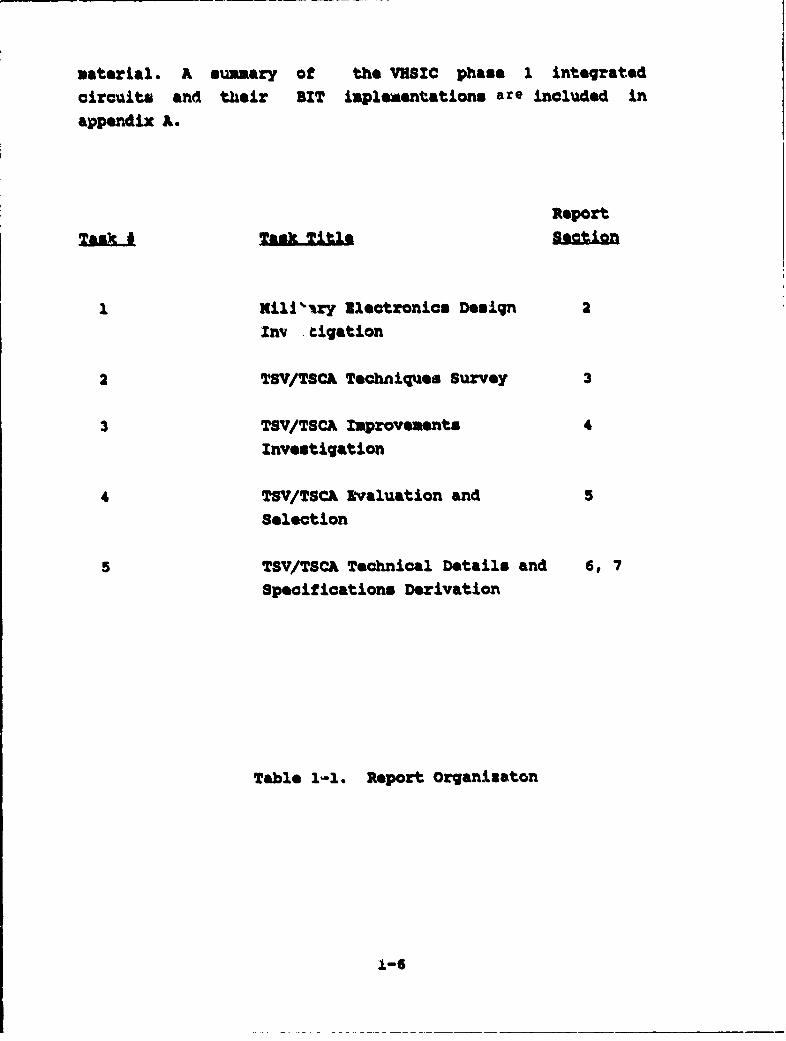
material. A suuaary of the VHSIC phase 1 integratedcircuits and their BIT impleaentation8 are included in
appendix A.
Report
Sls Section
1 Kil1-zy IleotronicS Design 2
Inmv igation
2 TSV/TSCA Techniques Survey 3
3 TSV/TSCA Improvements 4
Investigation
4 TSV/TSCA Evaluation and 5Selection
5 TSV/TSCA Technical Details and 6, 7Specifications Derivation
Table 1-3. Report Organisaton
1-6
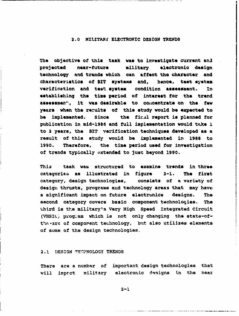
2.0 MILITARY ELECTRONIC DESIGN TRENDS
The objective of this task was to investigate current andprojected near-future military electronic designtechnology and trends which can affect the character and
characteristics of BIT systems and, hence, test system
verification and test system condition assessment. Inestablishing the time period of interest for the trend
assessmeor4-, it was desirable to concentrate on the fewyears when the recults of this study would be expected to
be implemented. Since the final report is planned for
publication in mid-1986 and full implementation would tp.ke 1to 2 years, the BIT verification techniques developed as aresult of this study would be implemented in 1988 to1990. Therefore, the time period used for investigationof trends typically extended to just beyond 1990.
This task was structured to examine trends in threecatagorics as illustrated in figure 2-1. The firstcategory, design technologies, consists of a variety ofdesigin thrusts, programs and technology area3 that may havoa significant impact on future electronics designs. Thesecond category covers basic component technoloSies. The
third is the military's Very High Speed Integrated Circuit(VHSIL, progl'am which is not only changing the state-of-the:-arc of component technology, but also utilizes elementsof some of the design technologies.
2.1 DESIGN TEýIUNOLOGY TRENDS
There are a number of important design technologies thatwill impect military electronic dssigns in the near
2-1

q
,� .�
'a
hm1mm
'a 'aS
q 'ap 'mm
I' CUmarn 'mmea a
'mm Sa 'U'a a 0
'U 'a 'U 'U
ILl 'a'mm
S
S3mm
'U'mmS ab
'a*mm�)�� limb
'a ab�'a mm.
�'aQ, 'aa�saa
'a'0**mm� 'Ummmm'UI S
55��mmm S
2-2
Luture. Thoke identified for this study are:
a. Computer-Aided Engineering
b. Artificial Intelligence
c. Modular Avionics Packaqing
d. Pave Pillar
e. Integrated Diagnostics
f. Architectures
q. Data BusesEach of these will be examined and evaluated as to itsimpact on built-in test design in the following sections.
Conclusions for the various design technologies may be
contradictory since they are drawn only from evaluation
of the individual technology, but these will be resolved
in a discussion of the overall impact of these design
trends in section 2.4.
2.1.1 Computer-Aided Engineering
The use of computers in the electronics design process has
increased beyond the Computer-Aided Drafting capability.
Computer-Aided Engineering (CAE) provides the designer
with a coaputer design assistant to do bookkeeping type
tasks, verify that designs conform to design rules, check
for errors and manipulate data, artwork cr machine control
information. There are also computer tools that
simulate designs to verify operation before implementation.
The use of computer-aided engineering is increasingsignificantly, especially for the design of integrated
circuits. CAE is currently being used for Very Large Scale
Integrated (VLSI) circuit design, including VHSIC and gate
array design as well as the traditional roles of printed
wiring board design and assembly wiring generation.
2-3

The use of computer-aided engineering tools to performdesign for testability tasks is lagging, but is currentlybeing addressed. Soma integrated circuit design systems
provide the capability for automatic incorporation of test
circuits. This is usually tn the form of a set/scan
technique such as the system reported in reference (1).
For integrated circuit design, fault simulators exist that
can be used to verify the built-in test or generate the setof test vectors used by autosatic test equipment. Thesesimulators can also be used for subsystem design vhen
gate-level models of its components are available.
The future should provide for better computer-aided
engineering through incorporation of testability tools,
particularly at the subsystem and system levels.
References (2) and (3) recommend development of Computer-
Aided Design for Testability tools. Following thoserecommendations would provide for consideration of
testability in the early stages of design, resulting inthe development of more testable circuits, subsystems and
systems. One of the difficulties to overcome in
adopting these recommendations is to effectively model
VLSI devices used in the design of these subsystems and
systems.
To do this, the capability tc accurately model systems at
a level higher than at the gate level must be
developed. One strong reason for this is that gate level
descriptions of most VLSI devices are proprietary and not
available to the subsystem designer. A second reason is
that even when gate level models are available, computers
would not be able to handle simulation models of that
complexity. For example, if a subsystem contained 100 VLSIdevices of complexity ranging from 10,000 gates to
100,000 gates, the simulation of the subsystem would
have to be capable of handling 1 million to 10 million
2-4

gates. Even if the computer on which the simulation ran
could handle a model that la~rge, the execution timewould be prohibitive. Modeling devices and subsystems ata *higher level would help overcome these problems.
As a result of the predicted increase in the use ofcomputer-aidied engineering systems that incorporate
testability tools, the built-in test capability of future
systems will be improved. This improvement will be in theform of better fault coverage and automatiQ incorporation
of standardized BIT (e.g. set/scan registers).
2.1.2 Artificial Intelligence
Developments in Artificial Intelligence (Al) are rapidly
finding their way into practical applications in industry,
and efforts are currently underway to develop military
applications. The field of artificial intelligence
generally includes natural language processing, robotics,
machine vision, expert systems and other related fields.
Expert systems have already been used effectively in
industry for diagnosing electronic systems, examples of
which are cited in reference (3). Reference (3) evaluated
the possible applications of artificial intelligence to
testability and found several to be particularly cost
effective. As a result, a practical evolutionarydevelopment program based on that work was recommended.
The recommended program is based on government support for
the development of basic tools and application independent
rule bases for two primary efforts. These would be expert
systems hosted on engineering workstations, which are
becoming standard industry tools for a broad range of
engineering tasks. The first effort would be a computer-
2-5

aided design for testability system. This would give
design engineers access to the testability engineer's
expertise early in the design cycle at all levels of
circuit, subsystem and system cessign. The second would be a
maintenance expa.-rt design system which would permit easy
development of diagnostic expert systems either for
organizational level maintoenance or for use on automatic
test equipment. It would contain a set of metarules
(application independent rules) representing general
diagnostic strategy upon which the user would develop
application specific rules. The capability of developing
self-improving diagnostics is seen as a later evolutionary
step. Both of these applications of artificial intelligence
are expected to greatly improve the testability of
future military electronic systems through supporting
improved design approaches. In particular, they will
make the built-in test more effective and the design less
prone to containing hidden design errors.
There is, however, one area of concern related to
application of artificial. intelligence in military
systems. That is, tne validation of expert systems
embedded in the electronics, as an integral part of the
built-in test such as that under study in the Smart BIT
effort (4). Smart BIT would use an expert system rule base
to examine test data and filter out false alarms. Some
work has been accomplished in verifying the design of
expert systems (5) but no work addressing monitoring
of expert systems during field operation 'was uncovered.
BIT has not been developed for expert systems, but BIT for
the hardware hosting the expert system can be implemented
independently from the expert system application.
For expert systema incorporated as part of BIT, the design
can be verified using the same techniques developed for
other expert systems (5). monitoring the operation of an
2-6

embedded expert system for BIT will involve testing both
the hardware and the software. The hardware may be
conventional von Neumann computers, LISt Processing
(LISP) languag.q machines or,, ultimately, parallel
inference processoxs. Testing of conventional computers
will be accomplished the same as it is currently. It is
anticipated that special inference processors will use BIT
techniques similar to the best of what is in use n ow for
production systems or those for near-term new VLSI devices
(e.g. VUSIC). In either case, the testing of the hardware
is not influenced by the tact that-the software implements
-an expert system. The software can incorporate tests for
gross operation but detailed testing of software operation
will not be feasible. Software errors will need to be
corrected as part of design verification.
The risk associated with verification of a BIT expert
system and the monitoring of its operation during use will
be a key consideration in the development. of embedded
expert systems for BIT. it is unlikely that expert systems
will be embedded as pa~rt of a subsystem's BIT before 1990.
The initial impact of artificial intelligence on BIT design
will be its use in computer-aided engineering systems
as described in section 2.1.1.
2.1.3 Modular Avionics Packaging
The Navy's Modular Avionics Packaging (MAP) effort wasinitiated in the mid 1970's to standardize avionics
packaging. The motivation was to reduce life cycle cost of
weapon systems by using standard modules on a variety of
programs. The original thrust of the program 'was to
specify standard modules (circuit cards) for Air
Transportation Rack (ATR) style boxes. With the rapid
increase in electronics density, the emphasis shifted to an
2-7

integrated rack concept. The rack would contain
collections of standard modules (circuit cards), without
individual boxes enclosing functions. This could reduce
weight and volume requirements by 30 to 50 percent (6).
The modules would be interconnected to implement functions
and the functions would be interconnected through the rack
wiring. Power and cooling would be provided as part of the
rack design.
The integrated rack concept continues tV run into technical
problems with thermal management, electrical
interference between the interconnections, and
exposure of the rack and the modules to the environment
during maintenance. However it offers enough benefits that
development of the concept continues. For example, in the
Pave Pillar program (see section 2.1.4), the concept is
being evaluated for application on tactical fighters. As
part of this program, ARINC Research Corporation is
preparing a military standard for standard size line
replaceable avionics modules. These would take advantage
of surface mount technology and VHSIC components to
achieve high density.
The MAP concept could potentially make BIT more
complicated or require more BIT since failures would need to
be isolated to a module rather than a box. However,as circuit density increases, more complete functions will
be implemented on a single module, reducing the need for
additional isolation capability. The effectiveness of
BIT will be improved with implementation of the ARINC
military standard (to be approved around 1988) since it
will incorporate design for testability g'Jidelines and BIT
design requirements. This standard will address testing
at all levels, and include preferred methods for BIT,
use of a standard test bus, standard system
interfaces, autonomous module checking and module
storage of BIT maintenance data.
2-8

2.1.4 Pave Pillar
Pave Pillar is an effort sponsored by the Avionics
Laboratory of Air Force Wright Aeronautical Laboratory
(AFWAL) to define and demonstrate the avionics system
for the 1990's tactl cal fighter. Program emphasis is
two-fold. Increased performance, to counter the ever-
increasing threat, is to be achieved through greater
iLntegration of aircraft systems with defensive and
offensive avionics systems. Increased availability is to
be achieved through incorporation of fault tolerance and
reduction of maintenance requirements. Testability
issues have been considered throughout the concept
definition phase. The following are summaries of features
of the Boeing Pave Pillar concept that may impact future
implementations of built-in test.
Generally, the architecture consists of several groups of
processing elements interconnected by multiple, redundant,
h~igh speed, serial data buses. Nondigital information is
converted to digital form at the front-end of the system
and digital processing is used to the maximum extent
possible. Functions are distributed among the various
computing elements which are replicaited where necessary to
meet fault tolerance requirements. The groups (mission
management, vehicle management, etc.) are loosely coupled
via serial data buses or control elements. The serial
data buses will uso a new standard high speed bus
(>2014Hz), and the interconnections will be fiber optic
links. The computing elernents will make maximum use of
VHSIC devices. Common modules will be used whenever
possible, using software to tailor their functions.
Certain hardware elements will require unique modules. For
example, the cockpit displays will be unique because of
special form and function requirements. The total system
is expected to consist of approximately 250 modules of
about 40 different types.
2-9

Detection of failures within data processing computing
elements will make use of BIT incorporated in the VHSICdevices, but primary testing will be accomplished by
duplication of functions and synchronized comparison of
the outputs. In the signal processing elements, a data
flow architecture will probably be implemented and testing
will be accomplished by injecting test data vectors in the
data stream and testing for errors in the data as it is
processed. When a failure is detected, the module will
either report its failure or shut down, depending on the
type of failure. The failed module's task will then be
executed by a spare module. BIT hardware, other than that
incorporated in the VHSIC devices will be kept at a
mini-mum and system level test functions will be imri-emented
in software.
Each computing element will be packaged on a single card
module. A data processing module will include duplicate
elements for processing (CPU), memory, unique Input/output
(1/0), and serial bus I/O. Elements are duplicated to
provide for fault detection. Each operation is performed
by each member of the duplicate hardware set and the
results are compared. Disagreement indicates the presenceof a fault. This isolates the fault to the module level
because all functions are on the same card.
An additional feature is that there are only a few pins
(for power, serial bus I/0 and unique I/O signals) on each
card module. This significantly reduces failures due to
interconnections and makes isolation to the module more
straightforward. The modules will be installed in an
integrated rack (an adaption of the Modular Avionics
Packaging concept) that contairs sufficient power and
cooling for up-to 40 modules. The rack also provides for
interconnection between modules within the rack and fiber
optic interfaces to other rincks and devices.
2-10

Testing of the avionics was considered early in the
concept development. Thi's resulted in a system concept
that reduced typical testing problems. The problem of
interconnection failure is reduced by putting entire
functions on single cards and using serial communications
buses. The problem of module isolation in addressed by
putting whole functions on cards and duplicating the
ciruitry to provide fault detection. System failure rates
are reduced by use of serial buses, and interconnection
faults can be detected and isolated through the bus
protocol. Built-in test design is simplified due to use
of duplication within the module for the data processing
modules, and injection of test vectors in the signal
processing modules.
The trend in BIT design, as indicated by the Pave Pillar
approach, is toward simple duplication of the circuitry.
This is made possible by advances in circuit technology.
It not only provides for effective fault detection, but
also provides effective test system condition assessment
since a failure in either half of the duplicated circuit is
also a failure of the BIT and is detected.
2.1.5 Integrated Diagnostics
The integrated diagnostics effort was initiated by the
Department of Defense in the early 1980's in response to
diagnostic problems encountered in maintaining modern
electronic equipment. The problem is that specificationau
only called for automatic diagnosis of a majority of systen~
failures. This is accomplished using BIT or Automatic Test
Equipment (ATE). The remaining failures are generally
ignored. Therefore, when a particular problem
exceeded the automatic diagnostic capability, the
maintenance technician was left with only a schematic and
2-l1

an illustrated parts breakdown, but no diagnostic guides.
This is an especially critical situation, because problems
that exceed the BIT or ATE capability usually tend to be
the more complicated ones.
The objective of the integrated diagnostics effort is to
develop standards and technology to provide an integrated
mix of BIT, ATE, maintenance aids and manpower management
to provide unambiguous diagnostics for all failures
expected to occur. The National Security IndustrialIAssociation (NSIA) has formed an integrated diagnosticsworking group to provide guidance to the Department of
Defense. The working group is to recommend technology
development, demonstrat~ion prvnjects, and policies and
standards for implementation of integrated diagnostic
concepts.
The impact of integrated diagnostics on BIT design is
uncertain at this time. More sophisticated BIT with better
diagnostic capability may be required. On the other hand,
it may turn out that a better interface between the
maintenance technician and BIT is more important than
bet-ter built-in diagnostic capability. The improved
interface could allow the technician to access test data
for analysis, as needed, rather than provide him with an
ena conclusion from preprocessed data. This interface
needs to be able to provide more information and better
ways of requesting and displayinig data than currently
available. Use of art3.icial intelligence (e.g., expert
systems' is a potential solution to this problem.
2-12

2.*1.*6 Architectures
Architectures of military electronics have a significantimpact on the design of electronic subsystems and hencethe built-in test. As illustrated in figure 2-2, thearchitecture of avionics systems is changing with the
trend toward distributed systems and digital
iwplementations. In early systems, all information wasdisplayed to the pilot who functioned as the system
integrator. Most modern systems utilize a central digitalcomputer to integrate and distribute information. Thepilot utilizes integrated data such as navigation data
integrated from a number of sources. Future systems, manynow in concept development, will consist of highly
distributed hardware and software. The hardware will bedistributed based on the sources of data and locations and
requirements for controls. The software also will bedistributed through the hardware elements. This allows for
even greater integration of functions thereby increasing
pilot effectiveness. It was estimated that in 1978, the
military avionics inventory was 90% analog and 10% digital(7). Systems currently being implemented are more than
half digital, with the specific amount depending on the
type of system. It is predicted that by 1998 avionics
implementations will be 90% digital and 10% analog (7).
BIT will also have to be distributed w.4.th the functions,
but system level BIT control is still necessary and will
have to use system resources, ile. buses, processors and
mass memory. More systems will incorporate fault
tolerance, and the BIT design will have to be cornpatible
with fault tolerance concepts. This means that more of the
BIT will need to be concurrent. It will have to operate
continually during operation of the subsystem or be
interleaved with other operations to detect failures in
time for the fault tolerant hardware and software to take
2-13

MONTr wff"O PCKI
SI.'!rP CPONRO. L * fOSl C"YT w • P StS
ANS LoB CEreAL MINETAL PCTRDLTo DIONTAL
* WIRtE: PROGRAMS * STORED PRO0GRAM * DISThIDUTD HIERARtCHICA.L* M•DCATI• ANALOG * CENTRAL PROCESSOR(S) STRE PRO3ktAM
PROCESSORS * COIW4JNICATION TfRU 110 * ItWAK•JT CENTRAL PROCESSOR(S)* JNTEGRATION ThROUN4 INTEGRATION TIROUSN * DISTRI3TED1 DEDICATEDPILOTP ISPAYS CENTRAL PROCESSORDSTOLY FUNCTIONAL TOCESSORS
* NO LRANCqk/Y PRqOGRAM * COW4JNICATION THP ]KS NEWRK* LITTLErt FAULT TEA S LARG SCALE USE OF REI4ZANCY
* NO DYNAMlIC S SONE FAULT TOL.ERANCE S FAULT TOLERANCE AND DYNAMIlCRECONFISURATION * NO DYlNAMIC IRECONFIGURATIONCAPAIILITY RECONFIGURATION I
Vto SIC T E* DISCRETEA ANA SS CAPAIILITY
HARDWARE * 1M5I AND LSI HRWR
Figure 2-2 P.vlonlcs System Architectures (7)
2-14

corrective action. BIT will become more critical and will
receive systems level attention early in the design
process. Existing PIT techniques are adequate to meet
requilrements of distributed systems.
2.1.7 Data Buses
Future systems, because of their distributed nature, will
contirnu* to make us* of the MIL-STD-1553B data bus or its
derivatives. The trend will be toward higher speeds and
the use of fiber optic transmission media. The bus control
and terminal interfaces, except for transformers and fiber
optic transceivers, will be reduced to single integrated
circuits. The effect of serial data buses and single
integrated circuit interfaces on BIT is that isolation to
the failed Line Replaceable Uni~t (LRU) becomes simpler and
faults (especially intermittent fault.) due to
interconnections are significantly reduced. There is,,
however, a need for reliable BIT as part of the bus
interf ace components in. order to properly diagnose bus
related failures. No new BIT techniques are required,
however the need to incorporate BIT in bus interface
components must be addressed during system design.
2.2 COMPONENT TECHNOLOGY TRENDS
Trends in electronic comiponent technology were examined to
determine impact on built-in test (BIT) design through
1990. This was accomplished by reviewing electronic
component technology trend information from in-house sources
and from recent electronics design trade publications.
The discussion of results addresses the forces
driving electronic component development, component
parameters of interest, and anticipated trends. it
2-15

includes an assessment of the impact of these trends on BIT
design.
2.2.1 Driving Forces
A significant factor in the component technology trendassessment is the trend toward digital implementations of
electronic systems. The continuing shift from
predominantly analog designs to predominantly digitaldesigns is the result of the teend in architectures as
discussed in section 2.1.6 and advances in large scaleintegration of digital circuits. These advances areresulting in dramatic increases in capability, as well asdecreases in cost and power requirements of integratedcircuits. This results in increased capability forimplementation of operational requirements and forinclusion of more sophisticated BIT capability.
The majority of digital computing applications over thepast ten years have used general purpose von Neumann dataprocessors, particularly microprocessors. This iscontinuing, but interest is increasing in non-von Neumannprocessors for a variety of signal processing functions.It is in this area that the majority of the displacementof previously analog implementations will occur. Table 2-1illustrates the variety of digital functions in militaryelectronic systems (8).
In addition to the expansion of applications for digitalelectronics, processing requirements are increasingsignificantly. Table 2-2 shows the expected growth inthroughput requirements for digital processors in severalapplications by 1990 (8).
Because of the trend toward the use of digital electronicsand the significant increases in capability required for
2-16

Table 2-1 Digital Functions in MilitaryElectronic Systems (S)
Militarysystems
Dig I :tj IFunctions I
Analog to Digital Cony. x x x x X x xIF Band Manipulation x x x x xData Reordering x x x xCorrelation x x x x x xFiltering x x x x x xAdaptive Filtering x x x xDetection and Integration x x x x x X xDisplay Formatting x x x x x x xData File Maintenance x x x xLogic and Calculation x x x x K x x x
Table 2-2 Expected Growth in Digital ThroughputRequirements for Various Defense Systems (8)
Computation RateRequired (MIPS)
DigitalProcessor Now 1990Function
System Management and Control 0.1-1.0 10-100
Radar 1-10 100-500
EO and IR Imaging Systems 10-20 200-2,000
Broadband Secure Communications 1 0-30 600-2,000Electronic Warfare 25-100 1,000-10,000
2-17

the future, the component technology assessment isconcentrated on digital components. Trends for analogcomponents are following those of digital components (i.e.greater performance and larger scale integration).However, no resulting changes to BIT techniques arerequired based on current indications.
2.*2.2 Component Parameters
The trends in electronic component technology wereanalyzed in terms of key component parameters. Thiswas because most trending information is presented in termsof these parameters and most of the parametersrelate directly to the primary performance of the devices.The following discussion of each of the key parax~tersincludes the significance of the parameter, the trends ingeneral and the relationship to other parameters.
Chip size - relates to the functional capability of thedevice. That is, for a given feature size, the larger thechip, the more there is on it and the mor* it can do. Chipsize has been increasing through successive levels ofintegration (Small Scale Integration (SSI), Medium ScaleIntegration (1151), Large Scale Integration (LSI),, VeryLarge Scale Integration (VLSI)) and will continue toincrease for the foreseeable future as the industry movestowards wafer scale integration.
Feature size - relates to the functional capability of the
device, in that the smaller the features are, the morethat can be put on a chip. Feature size also has beendecreasing and will continue to decrease, well through the
1990 time period. Ultimately, feature size is limited bythe physics of the materials, but that limitation will not
be reached until well after 1990.
2-18
Active elements per device - relates to the functionalcapability of the device and reflects the combined effectsor the first. two parameters. As chip size increases thenumber of active elements per device increases. For agiven *its, smaller feature size allows more activeelements per devic*. This parameter is most often used toproject trends in integrated circuit technology.
Performance - is a direct measure of device capabilitythat depends on the type of device. The most common arepropagation delay for logic gates, access time formemories and operations or instructions per second(usually in thousands or millions) for processors.Performance over a class of devices depends primarily onthe specific technology, that is the materials andmanufacturing processes used (e.g. bipolar is faster thanComplimentary Metal-Oxide Semiconductor [CI(OS]). For agiven technology, however, performance improvements can
result from changes in the manufacturing processes,especially those which permit reductions in feature size.The trends then are toward generally increasingperformance with significant increases resulting from newtechnologies.
Power - is of concern for applications with a limitedpower source or where heat dissipatio 'is difficult. Aswith performance, power depends primarily on the specific
device technology. In general there is a trade-off betweenpower and performance in selecting the device technology.
Devices with greater performance require more power.
Within a given technology, the more active elements there
are in a device, the more power it requires.
I/O pins availability - continues to be a limiting factor
in VLSI designs. Increases in functional capability and
device flexibility require more I/O pins. Also, it is
2-19

desirable to adid extra pins for test accessibility. Until
recently, most integrated circuits were limited to 40
pins, with a few going to 48, or 64. Now packages are being
introduced with more pins, especially leadless chip
carriers (up to 164 pins) and pin grid array packages (up
to 240 pins) (9).
2.2.3 Trends
The previous sections presented a general indication of
thlle expected trends for each of the major parameters.
Figure 2-3 shows specific trends predicted for the number
of active elements per device and the factors contributing
to it. It shows the increase in die size and the decrease
in feature size through 1990. These result in the number
of active elements per device shown by the curves. The
curves are for Random Access Memory (RAM) devices and
Microprocessor Units (MPU), the two most common and most
important digital integrated circuit types. Memory dE.,ices
have the greater number of active elements for a given
chip size because they have regular layout patterns and
relatively simple interconnections.
The curves are generated from information from reference
(8), and the data for wafer size, die size and feature
size are from reference (10). Projections from other
sources show slightly later availability for production
devices of a given capability, so figure 2-3 should be
considered as representing the earliest availability of
a device. (i.e. preproduction). Differences in projections
between sources reflect both levels of optimism and
differences in timing between working laboratory
versions, initial samples, commercial production and
military production of integrated circuits. The specific
availability of a device is not as important as the
2-20

r • i . . . ... ,i -,
IIs
~ CL
a U04
* a *aIeL I
1011110
S I
| g I a1Q
.a
f-4
a V4
s •
a2 a
* . a•
a a
SN a
- II S - Ia-,. , •, i• IS• e e i
,in ; w2-21

indication that the growth in device complexity willcontinue doubling approximately every 2 years through1990.
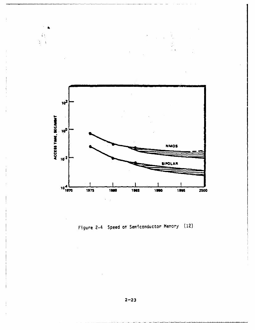
Similar trends can be fou-nd in the performance parameters.Figure 2-4 shows projected semiconductor memory access
time for N-channel Metal-Oxide Semiconductor (NMIOS) and
bipolar technologies (12). These indicate continuin~g
improvement through 1990,, and similar improvement can beexpected for gate propagation delay. The performance,parameter receiving the most attention, however, ismicroprocessor performance. Figure 2-5 shows the expectedimprovement in processing speed of 16 bit micro-processors
through 1990.
As was previously indicated, the power required per gate
in a device is primarily determined by technology, with a
trade to be made between power required and performance as
shown in figure 2-6. The exception is gallium arsenide
(GaAs) which will offer increased switching speeds for
pow~er dissipation comparable to NMOS0. Although production
of GaAs devices is now beginning, there will not besubstantial application of the technology in digital
systems before 1990. VLSI devices of GaAs will not be
available before then and use of GaAs will be limited to
special applications with unique requirements, due to the
cost of the devices.
It should also be noted that speed improvements in the
silicon technologies at the same power dissipation will
continue to be made through 1990 as a result of
improvement in manufacturing processes, especially those
that permit smaller more accurate features.
Power dissipation for integrated circuits is increasing
due to the increasing number of devices on the chip. This
is causing concern in packaging of the integrated circuits
2-22
I ' N•IOS
BPLAR
19' I IN 1" 1,, I" 200
Figure 2-4 Speed or Semiconductor Memory (12)
2-23

T
JJ-%t
° w
rw4r4)W94
CD uVý Ln
N- 4
S1.
ra
0
Cc-I
'-4
PC~
2-24.

-JUL
00
00
0-l 0-
00013
2-25

and in the design of circuit cards. For example, it often
involves careful placement of the heat generating
components closer to the cooling source (thermal
management program).
2.2.4 Trend Summary
The above saibsections summarize trends expected for the
most important digital electronic component
characteristics. The significance of the data for this
study is not that a specific level of capability is
available at a particular time, but the trend that is
shown. From the information collected, the trends from the
past five years will continue through 1990 with no radical
changes in technology. That is, there will be increasing
application of microprocessors in military electronic
design, and the processing power of microprocessors and
the density of memories will continue to increase,
allowing processing capability per unit volume to increase
correspondingly. Similar trends are expected for analog
components.
2.3 VHSIC TECHNOLOGY
The Very High Speed integrated Circuit (VHS IC) development
effort was initiated by the Department of Defense to push
the state-of-the-art of military grade integrated
circuits. The emphasis of the program Is to increase
operating speeds primarily through reductions in feature
size and to increase functionality by increasing the scale
of integration (more devices per chip).
The VHSIC program is important to the future of military
electronics design for several reasons. First, it is
anticipated that the technology, if not the specific
devices developed, will be used in a significant portion
2-26

of new military electronics design. The program is alsodeveloping the tools to permit easier integrated circuitdesign which should lessen the cost impact and makecustom designs more readily available. An important aspectof the VHSIC program is the mandated consideration of designfor testability. The program requires part of the chiparea be devoted to built-in test for the chip, but didnot specify how much should be reserved or what levelof performance should be achieved.
The appendix contains a summary of the various Phase IVHSIC efforts, including a description of the built-intest approach chosen for each of the devices. The mostcommon BIT technique was built-in signature analysis.Hughes, International Business Machines (IBM), Texas
Instruments and Honeywell all chose it as their *primarytechnique. TRW used set/scan registers for loading testdata and reading test results. Westinghouse partitionedtheir chips into test cells for which all of the inputsand outputs could be controlled. In some cases themanufacturers appeared to use BIT primarily to simplifymanufacturing tests. Some of the chips have limited on-line test capabilities for their parts, but all need to betaken off-line for the thorough tests. With the possibleexception of Honeywell's, the chips may be tested by anexternal processor in the system. Some of the processorele-ints may be tested as part of a regular timedoo!.ation. The Hughes parts require an external processorto compare the test results with known good results.Several of the other companies have the correct resultof a test built in to the VHSIC chip (probably in ROM) andperform the comparison on-chip.
The onl- 1IT verification done on any of the programszte"med j e fault simulation to determinse fault coverage.
Hughes does use self-checking comparators for some of the
2-27

tests on the Encoder/Decoder chip, but that is the only
on-line verification technique *described. Most of the
chips have not yet been fault simulated. The fault
coverage predictions in those cases are consistently
higher than for those cases in which fault simulation has
been completed.
From the higher level# the system must initiate self
testing of the circuits either on a time available or
scheduled basis. Contractors who designed large portions
of the rystems in which the chips were to be used were
able to include the capability to test the system
operation (e.g. signals passing from chip to chip) as well
as chip operation. But for the most part, the VHSIC partswill only respond with information concerning their own
health.
The VI.SIC devices have incorporated built-in test, but the
resources required to exorcise that capability when thedevices are incorporated into a system have not been
developed. These will need to be defined as part of the
VNSIC technology insertion programs for the VHSIC built-in
test to become effective.
2.4 IMPACT ON BIT DESIGN
There is increasing emphasis on design for testability and
design of built-in test for military electronics. This is
because of the high cost of maintaining equipment and an
increasing need for fault tolerant systems. Currently,
about one third of the life cycle cost of a weapon
system is expended on maintenance labor. This in likely to
increase due to the increasing complexity of electronic
equipment and decreasing skills of maintenance technicians
unless effective test capability can be incorporated into
2-28

electronic equipment. Even with more effective BIT, moreskilled technicians will be required to interact with theBIT. BIT should be designed to interface with thetechnician in a way that will allow him to improve hisdiagnostic skills. Current interest in fault tolerantdesign in a result of the need for high system
reliability to meet current and proj~cted availability
requirements. An essential element of fault tolerance issome form of accurat~e built-in test (including
replication of functional elements and voting). For these
reasons, design for testability and, in particular,
built-in test are being considered early in the concept
definition phases of programs. The desi~n for
testability process may be formalized with the release~
of the proposed Z4IL-STD-2165, Testability Programa forEl',ctronic Systems and Equipment. This would help
establish testability as & design discipline similar to
reliability and maintainability.
The design technologies all indicate an increased emphasis
in design for testability and the tools to provide it inthe design cycle. As such, BIT will becorz more effective
(greater fault coverage and less susceptibility to false
alarms) by becoming more sophisticated. The only
indication contrary to the trend of increasing BIT
sophistication is the Pave Pillar approach,, which
distributes functions among replicated computing elements
along with multiple,, redundant, high speed, serial data
buses (see section 2.1.4). This is however, an application
in a highly fault tolerant, highly integrated system
and not representative of all military electronics.
The concern for testability has not been fully reflected in
the design of integrated circuits. Newer, complex, of f-
the-shelf integrated circuits have incorporated built-in
test primarily for testing during manufacturing not for
2 -. 2 9

usa in application of the devices. There are someexceptions such as parity checks or coding incorporated insome memories, timing or error condition chocks in someprocessing devices and functional tests in some peripheraldevices (e.g. loop-back test for 1/0 devices). For the mostpart, built-in test is (and will continue to be)implemiented at the card, box and system level. BIT may beincorporated in some semicustom devices (gate arrays)since some CAD systems have the capability to automaticallyincorporate BIT, usually a form of scan technique.
Comprehensive impler-entation of BIT at the integratedcircuit level is part of the VHSIC program. However,before this capability can be used in a subsystem design,BIT processor elementi for control and nonitoring ofresults need to be developed. This would involvestandardization of chip-level SIT interfaces. In theinterim, because of the high level of integration ofcomponents used in designs, BIT design will bepredominantly functional rather than component oriented.That is, tests will be made to see that functions(arithmetic, I/0) are performed rather than testing toverify that individual gates are operational. Currentlythis is often implemented as an allocation of part of theprocessing capability of the equipment. With increasingprocessing power available in microprocessors, morecapability is being allocated to SIT. This will permitincorporation of smart SIT concepts, including (1) morestorage of failure data, (2) evaluation of environmentaland operational conditions, (3) filtering of transientfdults and false alarms, and (4) isolating intermittentfaults to the fnulty component. This, in turn, may lead toincorporation of a separate SIT processor in equipmentdesigns and ultimately, perhaps, to a SIT processorintegrated circuit that includes these capabilities.
2-30

3.0 TSV/TSCA TECHNIQUES
This section reports the results of a survey of the
technical literature related to BIT verificationtechniques. The survey included articles from the followingjournals:
a. IEEE Transactions on Computers,b. IEEE Transactions on Reliability,c. Journal of Digital Systems, "d. Computers & Electrical Engineering,e. IEEE Transactions on Circuits & Systems,
The survey also covered the proceedings of the followingconferences:
a. International Symposium on Fault-TolerantComputing
b. Reliability & Maintainability Symposium
c. International Test Conferenced. Autotestcon
e. Compcomas well as several national library data base searchus.
Overall, the review yielded a surprisingly small number ofreferences to BIT verification.
In addition to current journals, personal contacts atmajor United States universities were made to identifyany BIT verification work which was unreported or inprogress. A major finding of these contacts was that noBIT verification studies were currently included inuniversity research. However, several universityefforts are underway to develop new BIT systems, andwhile they are not working in the area of BITverification, researchers at these universitiesexpressed great interest in the results of this BITverification study. Another finding of these contacts
3-1

is the conclusion that none of the new BIT systemsunder development will cause a radical change in theapproach to BIT verification.
Personal contacts also were made with industry andmilitary organizations to determine what BIT verification
techniques are actually in-use or~ under development for
military electronics (and momo. commercial electronics)
that may not have been described in publications. These
contacts indicate widespread use of Failure Modes and
Effects Analysis (FMEA) and simulation (both modeling andphysical fault insertion) for test system verification, butlittle attention being paid to test system condition
assessment. The PMEA and simulation techniques vary fromvery casual to very detailed use depending on the type ofprogram, the company,, the personnel and the type of
equipmuent being designed.
Figure 3-1 shows a break-down of the major BITverification techniques found in the literature search. A
summary description of each technique is also provided in
this section.
3.1 TSV TECI -QUES
Test System Verification (TSV) involves those BITverification approaches for both the evaluation of BIT
systems during engineering development and for
qualification of BIT systems to verify compliance with
the tesitability requirements. They are formally applied at
the system and subsystem level but may be used at all
levels of development. There were four major types of
TSV techniques reported in the literature and confirmed by
the personal contacts: figures-of-merit, FMEA,
simulation, and statistical.
3-2

IciUL
I--rU)
3-3

3.1.1 Figures of Merit
A common approach to evaluation of BIT systems -involvesthe determination of the value of certain BIT Figures-of-Merit (FOM). This technique applies in the TSVenvironment.•A '979 RADC report (13) provides an excellent
review of tne • various FOM's available. There has beenlittle change s nce the report was published. The reportisolated 16 different, but in some cases related, BITFOM's:
a. Fraction of Faults Detected (FFD)b. Fraction of False Alarms (FFA)c. Fraction of False Status Indications (FFSI)d. Mean Fault Detection Timee. Frequency of BIT Executions
f. Fault Isolation Resolutiong. Test Thoroughnessh. Fraction of Faults Isolatedi. Mea" Fault Isolation Time
J. Maintenance Personnel Skill Level
k. BIT Reliability1. BIT Maintainability
m. BIT Availabilityn. System Maintainability
o. System Availabilityp. Mean BIT Running Time
The avaluation of these sixteen possible FOM's included inthe RADC report indicated that BIT availability, BIT miantime to repair, fraction of faults detected, and faultisolation resolution scored high on the evaluation
criteria of translatability, trackability, demonstrat-ability, applicability, and uniqueness. Two of these
FOM's (fraction of faults detected and fault isolationresolution) have been used extensively as TSV measures,
3-4
but they suffer from the problem of requiring either a
significant amount of operational data or use of complex
simulations to compute the FOM's. This makes them
difficult to calculate with a high degree of accuracy. The
1979 RADC report recommends verification of the FOM's by
field data collection or by demonstration as part of the
maintainability demonstration, except for FOM's, such as
time to test, which are verified by direct measurement. It
does not address how the test results are obtained, but
discusses at length the statistical analysis for selecting
sample sizes and for assuring demonstrated results verify
the specified FOM. These statistical analyses can be used
as part of a test system verification technique.
3.1.2 Failure Modes and Effects Analysis
Failure Modes and Effects Analysis (FMEA) is widely
applied to Test System Verification. Tasar and Ohlef (14)
suggested the use of a statistical FMEA to determine the
fault coverage of a self testing program. They assumed a
single stuck-at fault model. After performing a standard
FMEA using the gate level model of the entire system (the
operating circuit and its BIT systems), they calculate a
reliability table which shows the probability of failure
of each test point. A criticality table which contains the
probability of undetectable failures is then constructed.
Using these two tables they calculate an overall BIT
coverage value. The method they propose requires prior
knowledge of the probability of all possible failures.
Kreuze (15) proposed an FMEA-derived BIT analysis scheme
which will:
a. Ensure that all known major failure modes have
been evaluated and are detectable and isolatable by
BIT.
3-5

b. Provide a preliminary estimate of BIT faultdetection and isolation capability.
C. Establish second level BIT hardware
design requirements as the BIT sequence is
detailed.
d. Establish guidelines for BIT software development
e. Define operational Line Replaceable Unit (LRU)
interfacing requirements to facilitate BIT.
The flow chart which Kreuze uses to illustrate his FMEA
derived BIT analysis is shown in figure 3-2. He offers a
method to calculate the capability of the BIT system to
meet design requirements using:
% faults detectable - (ffr/sfr) X 100%
% faults isolatable - (ifr/sfr) X 100%
where
ffr - sum of fault failw-e rates detected by BIT
ifr - sum of fault failure rates isolatable by BIT
sfr - sum of all failure rates
Kreuze illustrates the application of his technique by
applying it to a typical digital Automatic Flight Control
System (AFCS) servo loop.
3-6

SPARTITION INTOFUNCTIONAL BL.OCKSJ
I IDENTIFY HARDWARE THAT IIRPLEMENTS EACH FUNCTIONj
IIDENTIFY FAILURE MODES OFEACH HARDWARE EU TIT
ANALYZE WHETHER BIT CANDETECT FAILURE MODE
IANALYZE WHETHER BIT CAN1ISOLATE FAILURE MODE
IESTIMATE FAILURE RATE1OF EACH FALURE MODE
I CALCULATE FAULT DETECTION/FAULT ISOLATIONPERCENTAGES AND COMPARE TO
PRORMANCE REOUWFEENTS
Figure 3-2 FMEA - Derived BIT Analysis (1 5)
3-7

Collett & Bachant (16) like Kreuze, propose a FailureModes, Effects, and Criticality Analysis (FMECA) for BITsystem verification. Using a functional level FMECA, theysuggest the implementation of the flow chart shown infigure 3-3. The BIT plan is generated from the systemlevel failure modes analysis and then the entire systemincluding the BIT circuit is subjected to a FMECA. Theyapplied this method to a number of designs at GTE Systems,and it produced design changes that improved the abilityto meet BIT requirements.
3.1.3 Simulation
Another approach to Test System Verification (TSV) of BITsystems which, in our estimation, is used frequently yetis rarely reported in the literature in this context, isthe use of simulation tools. The system operation,including BIT, is modeled and simulated under variousfault conditions to determine its performancecharacteristics. Benowitz, Calhoun and Lee (17)estimated the effectiveness of BIT systems at HughesAircraft using the Hughes SATGEN (Simulation and TestGeneration) program. They modeled the operationalsystem with its BIT and simulated all single stuck-at-land stuck-at-0 faults. Using this method they were ableto determine how many system faults the BIT system woulddetect. In one circuit, for example, using simulation theywere able to determine that the BIT system could detect89% of the simulated faults. Bastian, Hochwald and Suzuki
(18) utilized a similar technique to evaluate BITperformance. However, they decided that rather thansimulating all possible faults to determine the BIT faultcoverage they would gmnerate a sample of possible faultsand simulate this smaller set. The size of the sample set offaults was determined to be 25 in order to be 95%
3-8
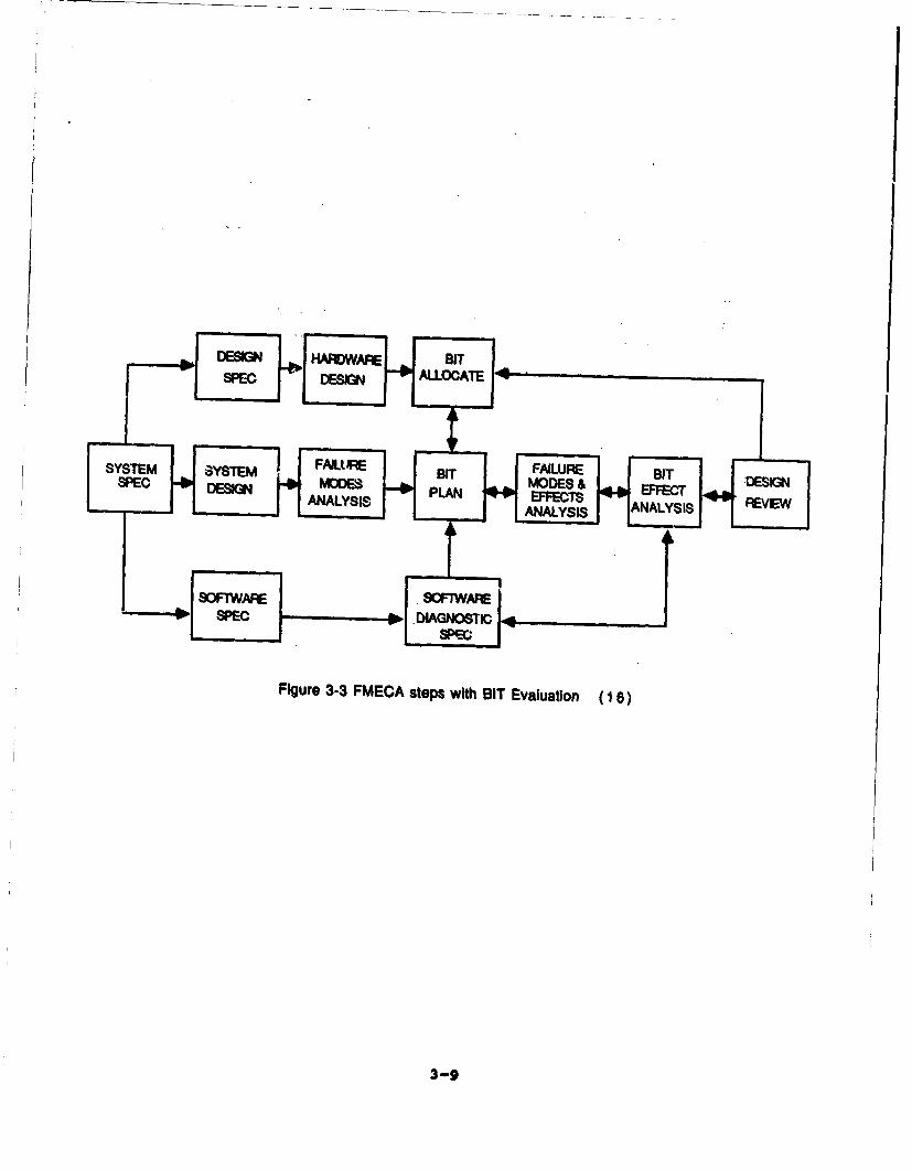
SPE DESIN ALOCAT
SYSTEM 3-3TE FMUECAseswt BIT Evaution( 131T
SPEC DESGN PMODS & EURET DSIG

confident that the BIT syntem could detect 90% of thesystem faults. This method significantly reduced the
simulation time.
While fault simulation is a straightforward approach tovalidating the fault detection capabilities of a BITsystex, it involves considerable time and expense to
simulate all possible faults. At this time, it is probablythe most common TSV approach. A recent improvement inthis technique, as reported by Bastian et al. seems toovercome the simulation time expenses. However,, theassumption made in their statistical analysis (that thenumber of faults detected is binomially distributed)has not beean completely demonstrated as valid or fully
justified.
3.1.4 Statistical
Another method of analyzing BIT performance invol~ves theapplication of statistical techniques. Most approachesreported in the literature are designed to zinswerquestions such as:
a. What is the probability of a BIT system generatinga false alarm?
b. What is the probability of a BIT system missing
a f ault?
c. What should be the time between BIT checks?
Two statistical techniques found in the literature
ara described below.
3-10
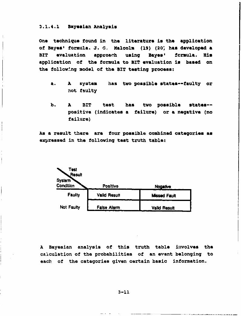
3.1.4.1 Bayesian Analysis
One technique found in the literature is the applicationof Bayes' formula. J. G. Malcolm (19) (20; has developed aBIT evaluation approanh using Bayes' formula. Hisapplication of the formula to BIT evaluation is based onthe follow'.ng model of the BIT testing process:
a. A system has two possible states--faulty ornot faulty
b. A BIT test has two possible states--positive (indicates a failure) or a negative (nofailure)
As a result there are four possiblet combined categories asexpressed in the following test truth table:
_esult
Systern e uCodlto Positive Nogastive ,
Faulty Valid Result Misad Fault
Not Faulty False Alarm Valid Result
A Bayesian analysis of this truth table involves thecalculation of the probabilities of an event belonging toeach of the categories given certain basic information.
3-11

For example, to calculate the probability P(FIT÷) that the
system is faulty given a positive BIT test result 'that
is, BIT claims it has detected a system fault), we would
use Bayeo' formula as follows:
P(FITPT+ IF -" P(F)P(FI+ )"P(Tr IF) - P(F)+P(TjFi • P(F)
where:
P(T÷IF) - probability of a positive test result
given a fault
P(F) - probability of a fault
P(T+I7) - probability of a positive test resultgiven no fault (false alarm)
P(T) - probability of no fault
Also, the probability of a missed alarm, P(FIT-), (that
is, system is faulty but the test is negative) is given
by:
P(FIT- PIF)- P(F)ý I P(I"F) P(F)+P(T" PI) PP(T)
where:
P(T IF) - probability of a negative testgiven a fault
3-12

P(T IF) - probability of a negative test
given no fault
To use the above formulas, we need to know the probability
of a positive BIT test result given that the system is
faulty and the "a priori" probability of a system failure.
For example, assume that a BIT system is installed in a
circuit and it has been determined that the circuit has a
probability of failure of 1% (P(F) - .01). It has also
been determined that the BIT system has a 95% fault
coverage (P(T+IF) - .95) and has a specificity
(probability of false alarm) of 1% (P(T+ IF) - .01). Then
the probability that the system has actually failed given a
BIT alarm is:
P(FIT +) (.95) (.01)
(.95) (.01) + (.01) (.99)
.4896
This illustrates a surprising result that Malcolm (19),
(20) discusses at some length. That is, that a BIT system
with a high degree of fault coverage may still produce a
high percentage of incorrect results. A look at the effect
on the BIT false alarm rate of improving the reliability
of the system is shown in figure 3-4. As figure 3-4 shows,
the more reliable the system, P(F) approaches 0, the lower
the probability that the system is faulty when BIT
indicates a system failure. Therefore, the effectiveness
of BIT depends not only on coverage but also false alarm
rate and the reliability of the system.
3-13

PROBABIULTY OF A FALSE ALARMGIVEN A POSITIVE TEST RESULT
1.0
P(FIT+)
.5-PROBABIUTY THAT SYSTEM IS FAULTYGIVEN A POSITIVE TEST RESULT
i I I I ii i
.05 .1 .15 .2 .25 .3
Probability of Failure, P(F)
Figure 3-4 Effect of Reliability on BIT Performance
3-14

The other side of this Dayesian analysis is vhat is the
probability of a system being faulty and the SIT failing
to detect the error? Assuming the same values as in the
first example the result is:
I- (.05) (.01)P(FlT- ) -- •
(.05) (.01) + (.99) (.99)
.00051
3.1.4.2 Markov models
Another statistical approach to TSV is the use of a Markov
model to analys:e the performance of a BIT system. Xarkov
models view the system as a series of states where a state
describes everything we need to know about the system at
any instant. The behavior of the system is modeled as a
series of transitions between states where the Xarkovian
assumption is that the probability of making a transition
to any state in the system depends only on'the presently
occupied state. A good introduction to Xarkov models can
be found in the book by Ronald Howard (21).
Capt. Gleason proposed a measure of BIT performance called
BIT accuracy (22) based on a Markov model of BIT system
operaticn. His approach could lead to a TSV measure. He
assumes that the system with BIT is in one of four states:
3-15

g 0o System functionali No false alarm
all System functional; False alarm
82: System nonfunctionalt Detected
failure
S3t System nonfunctional: Undetected
failure
The transition between the states are represented by the
probabilities:
XFA At- probability of a false alarm in
tine period At
SDA t - probability of a detected failure in
tine period At
U At - probability of an undetected failurein tine period At
The Narkov model for this system is expressed in the statediagram and transition matrix shown in figure 3-5. Theprobabilities of the system occupying each state 80 to 83as a function of time are derived from this model and aregiven by:
3-16

XFA~t )tUAt
SiI3
so Si S2 S3
SO XFAAt Xt AAA
S 1 0 1 0 0
S2 0 0 1 0
S3 0 0 0 1
Figure 3-5 State Diagram and Transition Matrix for BIT
Operation Model (22)
3-17

PO(t) -W "(* U +X D + "FA) t
X L LFA [1-0 ";U+ )'D + XFA~tP2 (t) - [1_+ -- X + XFA
I DOF .('U÷ •O •F~t
U_____ +ý. +).FP2 (t) " )u+'D• FA [1.. D F J
P3 (t) X U "'U +D + )'FA)t
U+ " Du÷ a÷ [-. "+ (u]
Gleason suggests that BIT accuracy is given by:
PA (t -P o ,'+ P2(t
"- ( )U+ )" + X'FA )t XD _ [1.e" )LU+ -XD + )LFA )t]• ,e+ I,+
U+ 'D+ "FA
That is, BIT is operating correctly when the system is
functional and there are no BIT false alarms or when theBIT correctly identifies the failure of the system. Theother states, false alarm or undetected failure, indicatedthat the BIT system has failed.
3-18
This Markov model assumes knowledge of AFA, hD and XThis information could be either based on experimentalresults or derived from some other TSV technique.Therefore, the Markov Model serves only as an analytical
extension of other possible TSV techniques.
3.2 TSCA TECHNIQUES
Test System Condition Assessment (TSCA) involvesdetermining the health of the BIT system under operatingconditions and prior to maintenance. It is required at thecircuit card, line replaceable unit and subsystem levelsto support depot level testing and at the subsystem andsystem levels to support organizational level testing. Inaddition, the necessary TSCA capability must be providedat each level of hardware implementation to support thenext higher level of hardware assembly. The focus of thisstudy is toward TSCA implemented at the subsystem andsystem levels. The TSCA problem is different from TSV inthat measurement of the testability parameters is nolonger required. in this case,, the interest is indetermining if the BIT has sustained a failure affectingits performance. There were two major approachesidentified in the literature search: the use of self-checking checkers and fault insertion techniques.
3.2.1 Fault Insertion
A form of BIT self-verification involves the addition of aforced failure mode into the system design. That is, the
BIT system generates simulated failures in the system.
Then the BIT goes through its standard check-out routine.if it detects the simulated failure then the BIT isassumed to be operating correctly. if it fails to detect
3-19

the simulated failure then the BIT has failed. This
technique is best suited for TSCA since it can be utilized
for self-verification of equipment in the field. Often,the forced failures are simulated in software. However,
Ramirez (23) has quggested a simple hardware mechanism for
injecting the failure directly into the system. Such a
mechanism is shown in figure 3-6. It involves a simple
flip-flop which forces the multiplexer to select the
stuck-at input condition. The. BIT then runs its normal
test sequence and if it fails to detect the forced failure
it flags itself as "failed." These flip-flop/multiplexerunits could be installed at several locations in the
circuit.
Similar implementations of forced failures are reported
elsewhere. For example. Siewiorek and Swarz (24) report
forced error conditions in the CPU and forced parityerrors in the memory of the DEC VAX 11/780 to test theBIT. They also report fault injection capability,implemented in both hardware and software in the SperryUnivac 1100/60.
3.2.2 Self-Checking Checkers
Another method of TSCA for BIT involves the development of
Self-Checking BIT systems. Breuer (25) defines a totally
self-checking circuit as a circuit which is both faultsecure and self testing. This is accomplished by
incorporating additional logic to encode the operationand, if necessary to decode the result. The followingdefinition of a fault secure circuit applies to circuits forwhich a set of allowable outputs can be specified. An
output not in that set is termed invalid. For any input,
only one output from the allowable set is the correct
3-20
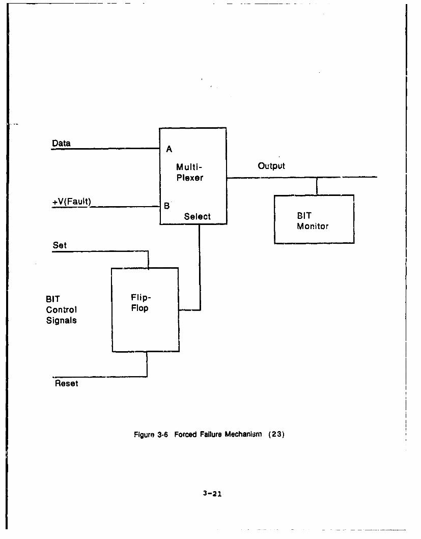
Data A
Multi- OutputPlexer -
+V(Fault) ,,B• I -I
Select BITMonitor
Set
BIT Flip-Control Flop..Signals
Reset
Figure 3-6 Forced Failure Mechanism (2 3)
3-21

output. A circuit is fault secure if, for any fault
and any allowable input, the output is either (1) the
correct output (if the fault does not affect the specificinput) or (2) an invalid output. That is, a fault willnever produce an output that is an allowable output but is,in fact, the wrong answer for the given input. A circuitis self testing if for any fault there exists anallowable code input which detects the fault. As the
definition indicates, totally self-checking checkers usecoded data so that an error forces a detectable, invalidword at the output. A totally self-checking BIT systemwhich failed would produce only detectable invalid words atthe output, hence, its condition could always be
determined by the nature of its output.
There are a variety of codes in use in self testingcircuits. The most common and well known are the paritytype codes. Other codes include residue codes and groupcodes. A review of the literature indicated a large
amount of theoretical work is currently being undertakento develop new coding systems for self-checking checkers.In addition, there is some work reported in the
application of the self-checking approach to BIT. Forexample, Fujiwara (26) proposes a new kind of e-&rorchecking scheme for use as a combinational circuit BITsystem called a group-parity prediction (GPP) checker.
The system is designed to monitor a multiple output
combinational logic circuit by partitioning the output
into several groups and calculating the parity of eachgroup. The calculated par'lties are compared to the
parity predicted from the inputs. It has been shown that
this method offers a high degree of fault coverage forcombinational logic circuits. In addition to detecting
failures in the monitored circuit, the GPP checker is also
self-testing with respect to any sing'.. internal
failure. Fujiwara's example system demonstrated a 98.1%
3-22

self-failure coverage and a !15.9% monitored system
fault coverage for an Arithmetic Logic Unit (ALU)Controller.
Hughes, McCluskey & Lu (27) have developed a totally self-
checking comparator circuit which could be useful in a BIT
system that involved the monitoring of duplicatedcircuits. Such a BIT approach would signal an error when
the duplicated circuits generated different outputs. A
totally self-checking comparator would also monitor itselffor internal errors and report them to the user.
Sievers and Avizienis (28) have developed a method to
design totally self-checkinq functions in CMOS and NMOSarrays called general logic structures (GLS). A GLS is a
two dimensional array much like a Programmed Logic Array
(PLA) only the GLS uses a k-out-of-2k code to achieve the
totally self-checking feature. They found that the GLS
NMOS array was totally self-checking, but the self-
checking attribute of the GLS CMOS array was sensitive to
the input patterns.
3.2.3 Other Techniques
While not directly reported in the literature, personaldiscussions with engineers working in the area of BIT
design has lead to the identification of two additional
approaches to test system condition assessment. One method
involves BIT systems where a single processing element is
dedicated to a BIT function. Often such a processing
element will have self-checking software which performs a
diagnostic run when the BIT is powered up. An example
application is a microprocessor implementation of BIT
which acquires test data and evaluates the results to
determine the presence of failures. The self-checking
3-23

program then would perform a checkswr. teat of the memorycontaining the BIT programs and a teat ofi read/write
memory by writing teat patterns into memory then reading
and verifying the teat patterns. These teat. verify theintegrity of the BIT function (i.e. the BIT programs) and
the operation of the microprocessor. Such an approach
provides a check of the BIT status prior to BIT usage.This approach is limited to systems with BIT implemented
as a separate processing element.
Another method for TSCA is a simple fail-safe approach.
The output of the BIT system is initialized to a "failuredetected" message prior to testing. The BIT system mustsuccessfully complete testing then take a positive action
to change the "failure detected" message to a "no failure"message. The result is a limited fail safe capability in
that in most cases of BIT failure, BIT will not be
successfully completed, the message will not be reset,
and the user will be notified of the failure. of course,
the user will not be able to determine from the message if
the failure was in the BIT or the unit under test.However, it does reduce the problem of BIT failing in a
mode that always indicates a "no failure" condition, sothat when a unit under test failure occurs,, BIT does not
indicate the failure. An example is memory tested by a
parity circuit where the result is stored in a flip-flop.
At the start of a test the flip-flop is reset to zero and
on successful teat is set to one. If it doesn't get set to
one, then either the memory is failed or the parity
checking circuit is not working. This approach is
applicable to any type of BIT system where the results are
stored in a flip-flop, a register or a memory location.
3-24

4 0 TSV/TSCA IMPROVEMENTS INVESTIGATION
This section reports several suggested improvements tozurrent BIT verification techniques identified in the survey.After an initial review, three of the improvements wereselected for further development. The details of these
developments are reported in sections 6 and 7. The specificmethods covered in this section are summarized in Table 4-1.
4.1 TSV TECHNIQUES
Additional FOM's can be derived by combining existing FOM'sin various ways. An illustration based on Gleason's Markovmethod is given below. However, major drawback to FOM's ingeneral is that no easy way is known for obtaining accuratevalues for the parameters used to calculate them. Until moreprogress in this direction is made, it is futile to pursueFOM's any further.
FMEA and simulation techniques are also candidates forimprovement. Possible directions for development work to
improve these techniques are presented in the followingsections.
4.1.1 New Figures of Merit
A BIT Figure-of-Merit could be used to provide a measure ofpredicted BIT performance. As indicated in section 3.1.1,
FOMs have been developed for use as TSV measures. Thisresearch effort briefly considered the possibility of
modifying several of these FOMs in order to produce a new TSV
technique. For example, the basic Markov model suggested byGleason (22) (see section 3) was analyzed further to produceseveral new FOMs relating to various aspects of BIT
performance.
4-1

------ ---- ---- ------ --- -- -----'1 -I 41 0 0)4)~~~~ r-40 ' H.)
01460 144 U004 ~ 1) $ 4 r. $40 l r-4
N0 45 tW* -r FHO 1644A0004 0 040 14.00 $40' r4~ H 0U Hr 0 .
1040 VOH H4O 00- 414 04~0 0 OH A0 la 4 %4 -4 V 0 )E-4 -4 t
0 "4 0 f6404 F 4)4 V 00 '0 0a >H r4I 0$4'0. 0)0 OH H4Jq- 001 0 m g4VE
e I t0 0 q r. 0 00 r l0 to 41 0 $4 4) r. C~ 070 4) 41p 4)A $4 10 V0 -4 0) 0 to 0 H -'H 41 V- 0 FAr-
Z we H' 4-)A 4-) 14 '0l $. H 04V 04 . i19 r.to9o 10 4JP4 4 f Hr 640 000 04J M 0 W100 QrI-H 14 0
00.H00M
eta r o0 -2o 0 W0 00V 0 t0 -Vo4 A0 0 10H a0 .0 Q'0H ptr 044Or 0 04M o
H r~ 1 *-0 004 004 1O0
04 0 0 40~ -'U i. 0> 0~ '-r. 04.c 04 r.0 V14 01W 00P.0 .
010 0 r
0 >0) 4) 0' 04 t01t'0 Vu-404 1-4 EM 4 t 0 "~I, H- - -i q0 r P @ V~0 H 0 E4- 400 4 1)
OMO eg 0.4* > OM4 0H44P 0 0 H >H 4~ 0
u 4)~ 0 1 0. 0eG 4) 4) f -t -HInE V0 4) 4)'4 IAP 0 4)A4HE4$ #
4) HH.I0 4)
~~'6-4~~E- >10. ~ HH 4H
0 ?A4 00-
100 '0 10E4 HOj 0A0 0:U .0 f" H 4 ~ r4.- 44 H H44.H
4J to 4 I E-4)- U.0 m0 a0 0 $04) SO 0 V14( i4~ 0~ 3t >0 )t
C t $40 44) m a - 1 4 r0%
0 H 0d- . - - 40H H- dV0 4 4t 0H44) 0r Hr 4V : : 94 rH% to 04-4-r'J-4-
404) I 4r 0001 q 04"4 319"V 0 - A faa- 4 CC~~ ~ ~ ~ 04(H 1r 14 -
00 0
414-0

One possible new FOX based on Gleason's model was suggestedby the work of Spillman (29). Gleason's model of BIT systemscontains four states, two representing correctly operatingBIT and two representing fault states. Spiliman's new FOMrepresents the average amount of time the operating BITspends in the two correct states. It is determined by firstcalculating the mean holding time for each of the two BITcorrect states and then averaging the two values. The meanholding time is the average amount of time that the system isin any given state. It is given by:
" • In , (I
wy) L w(i)
where Ti - mean holding timewi - y (probability of transition from state i to
J~i stato J)
i "M (probability of transition from state j toJ*i state i)
The naw FOM is the average of the mean holding times for thetwo correct states S and S in Gleason's model. It is
0 2defined as
A (T + T2)/2o 2
" i -WO In (!22n ww 2o Wl2)
For example, consider a system in which the probability of
system failure over an hour period is .01, the BIT coverage
4-3

is .99, the probability of falas alarm is .01 and the system
is always repaired if a failure is detected. Figure 4-1
shows the state diagram and transition matrix for this
example.
In this case,
W PA + D + U - .01 + .0099 + .0001 - .02o F
v -i0
W-2
92 .0099
Then A - 1/2 C-Lj In C )+ in (. 0099)]
- 95,5 hours
As with the discussion of Harkov models in section 3.4, the
probability of fault detection and the probability of a falsealarm need to be determined by other means.
Beaudry (30) has also suggested some performance related FOMs
that may be adapted for Gleason's Xarkov model. Theyinclude:
(1) Computational Reliability(2) Computational Availability(3) Mean Computations Before Failure
Computational reliability, R(t,T), is the probability that
the system will correctly execute a task of length T startedat time t. Computationil availability is the average number
of computations the system wili correctly execute in a given
time interval. The mean computations before failure, MCBF,
is the average amount of computation available on the system
before a failure. In terms of a BIT TSV technique, these
4-4

~~1-( X.FA+ X. D+ X U)
/•,-.•• U "(1-.99) (.01)
1 2
(,FA+ D D+ •,U ) FA )D •U•
Transition = 0 1 0 0
Matrix 1 0 0 0
0 0 0 1
Figure 4-1 State Diagram and Transition Matrix
for Example of Modified Gleason FOM
4-4
three measures could be interperted as BIT reliability, BITavailability, and the mean number of correct BIT decisionsbefore a failure. All three of these measures emphasize theperformance of a BIT system over time rather than thepresence or absence of errors as in Gleason's model.
After a preliminary investigation it was determined that aBIT Figure-of-Merit approach would not provide an effective
TSV technique. Before Gleason's model of BIT pearormance can
be used to generate an FON, the exact values of thetransition rates between the four BIT states must be known.There are no known methods to accurately calculate theserates. They can be estimated to questionable degrees ofaccuracy from operational data. However, such estimatesrequire long-term observation of the working system. Sincethe FOM would be used as TSV measure, the working system maynot be available and if it is, the obser-ation time may beexcessive. As a result, further investigation of BIT FOMs aspossible TSV measures was discontinued.
4.1.2 Test Repetition Methods
If the goal of a BIT system is to detoct intermittent faults,it is necessary to allow the BIT system to apply its test
repetitively so that the BIT will be operating when theintermittent fault is active. The problem from a TSVperspective is to verify that the BIT does repeat itselffrequently enough to detect intermittent faults.
Spillman (40) has derived a formula describing fault
behavior, from which the test repetition rate to detectintermittent faults can be calculated. The formula is based
4-6

on the following two assumptions:
(1) Well-behaved Faults
The assumption is made that the transition from a
fault-free state to a faulty state and the
transitions between faulty states occur
instantaneously.
(2) Siuael-Independent Faults
It is assumed that the occurrence of an intermittentfault does not depend on the nature of the signals
in the circuit.
Both of these assumptions are commonly made to simplify the
study of intermittent faults and they both seen reasonable in
light of the observed behavior of intermittent faults. If
intermittent faults occur at rate A and disappear at rate •,
the probability of a transition from a to n "active"
intermittent faults is given by euation (1). N is the
maximum number of multiple "active" intermittent faults
allowed in the system.
Pi1 (I- ML + 2a _)Bj )I(!)(IN- -N-I1) j1 1-\2cos(x4 N+1)+*
I(1-6 N+i -
where a /A- the birth rate for intermittent faults;
- the death rate forlntermittent faults;
- -(A+#A)t + 2t(AA) c•os(jw/[N+l]).
1/2A (a)- sin(mj - /[N+I]) - a sin(j(m+l) ir/[N+1])
B (a)- sin(nj w/[N+I]) - a i/2sn(j(n+l)r/[N+l])
4-7

When t- -, equation (1) becomes:
n-NPnm .Pm. (14. (2)
which represents the probability that the system evolves from
having m active faults at some time to a steady state
condition with n active faults. These expressions reduce to
the single fault case found in the literature when N - 1.
The test repetition rate, K, is given by equation (3):
Iog(1-CL n )
1l[2-P (t)n ] Pn3log I I-Pn II
where CL is the confide.ic, level for the decision "the
circuit is fault-free" if it passes all K test applications,
and t' is the time between test applications. The derivation
of equation (3) can be found in reference (43). For example,
an engineer testing a circuit for intermittent faults may
want to be 99% confident (CL = .99) of detecting a singlenfault in a triple fault environment with A =.008 and j = 1.0.
First, equation (2) would be used to calculate P1 = .00794.
If the test is applied one second apart, P 1(1) = .36851 from
equation (1). The test repetition rate is found trom (3):
I~g(.01)
Iog(.99495)
- 909.61
The engineer would apply each test in the test set to the
circuit 910 times. If a fault is not detected then he would
;e 99% sure that the circuit is free of intermittent faults.
4-8
SJIS- -,• ! ,• -- '!I .. ' •:'••t 3 •!~ •' •1!•- ,ununh/w•l~l"~ l•"ln ii q li3Ig .l• ' g•'tiJ•I I

The test repetition rates produced by the model could serve
as a guide for determining BIT performance under intermittent
fault conditions. However, TSV approaches for permanent
faults need to be better understood before exploringintermittent faults, so this concept was not pursued further.
4.1.3 Extensions of FMEA
The most popular Test System Verification method is FailureModes and Effects Analysis. However, its use for TSV suffersfrom lack of standardized approaches and lack of accuracy.RADC's Automated Advanced Matrix FMEA effort has attempted to
develop a system for automated FMEA with the objective ofstandardizing the technique and reducing the cost throughautomation. There is still need for additional work in theBIT evaluation portions of the Automated FMEA. Betteridentification of failure modes and their effects is stillneeded, especially for VLSI and VHSIC devices. After apreliminary investigation, it was determined that FMEA
approaches need additional improvements before they can beadapted to a TSV techrique.
4.1.4 Advanced Simulations
Simulation techniques have the greatest potential to provideaccurate and economical test system verification. Simulationhas been used in the past for TSV and continues to be usedextensively in the design of integrated circuits. However,its use for TSV at the subsystem level has become impracticalbecause of the increasing use of VLSI devices. Pastsimulation techniques used gate level modeling, but for manyVLSI parts the gate level models are n,t available. Also the
4-9

complexity of tcvday's and future subsystems v.ould make gatelevel simulation impractical. A significant amount of
computing resources would be required to test a reasone'ble
fault population. Suppliers of simulation hardware and
software have been addressing these problems, because the
size of VLSI devices is puttir~g greater demands on simulation
capability. Advances are needed to increase the size of the
system that can be mod'4led and to speed up the simulation.
These include methods of simulating the independent effects
of many faults at the same time, methods of rei~oving
equivalent faults from the fault set and the use of special
hardware accelerators. These hardware accelerators are
special-purpose computers designed to execute logic
simulations and can increase execution speed by several
orders of magnitude. A summary of the current state of the
art of logic and fault simulators is given in references (31)
and (33).
The above advances in simulation technology do not however
address the problems of simulation at subsystem or circuit
module level. The most significant problem is the enormous
size of gate level descriptions of ISI and VLSI devices.
Two recent advances in simulation technology have potential
for resolving these problems. The first is the use of actual
hardware as part of the simulation and the second is the use
of behavioral simulation.
4.1.4.1 Hardware Simulation
This approach models portions of the circuit using gate level
simulation techniques and uses real hardware for the
remaining portions. The motivation for this is to be able to
simulate a subsystem or circuit module that consists of a
combination of custom logic and off-the-shelf LSI devices. A
diagram of this type of simulation system is shown in figure
4-10

4-2. The simulation host interfaces to a couplex hardwareadapter and the hardware adapter allows the hardware devices
to interface to the rest of the simulation. The simulationsystem specifies whether each pin operates as an input or
output or both. As the aimulation progresses, signals are
passed to the hardware devices and are received frow thehardware deviceb. When performing fault simulation to
determine test coveraqe, faul.ts are inserted in the logiclevel simulation portion In the conventional manner, but
faults for the LSI and VLSI devices can only be inserted atthe interface pins of the hardware adatitor. Hence only
faults at the I/O pins of the devices can be simulated not
faults internal to the device.
This permits simulation of a subsystem which includes the useof LSI and VLSI devices to be developed with substantially
less effort than would be required if the LSI and VLSIdevices were modeled at the gate level.
SIMULATOR HOST SIMULATIONMODEL
HARDWARE LSI
ADAPTER ORSIMUIALTION
VLSI
DEVICES
I ,
SEVERAL HUNDRED PINS
Figure 4-2 Simulation Testbed Incorporating Hardware Elements
4-11

4.1.4.2 Behavioral Level Simulation
There has been recent interest in development of higher level
modeling ca~pability for use in the design of 1.91 and VLSI
devices. This is because IC designers need a tool to easily
model a complex circuit early in the design cycle. Modeling
at a higher level allows the designer to make architecture
traides, check performance and permit parallel development of
associated hardware and software without modeling at thedetailed design level. Figure 4-3 illustrates the levels at
which electronic systems can be represented and described.
It also shows samples of simulation tools applicable to the
various levels. There has been recent interest in developing
behavioral level simulators for the design of LSI and VLSI
devices. 1,34) (35).
Suppliers of simulation systems are developing behavioral
level simulators to respond to the need. Most provide a
special purpose modeling language based on popular general
purpose programming languages suach as C or Pascal, with anincreasing interest in Ada. The behavior model languages
need flexibility, but have to be structured for use bydesigners who are not expert programmers or simulationengine irs. These behavioral level models can be integratedwith gate-level models for a complete model of a subsystem.
There is additional need for improvements to behavioral
simulation languages to address test system verification
needs. First, continued work is needed in developing a
structure that is easily usable by design and systemsengineers. Second, a capability for modeling failure modes
(no longer definable at the gate level) in a realistic manner
is needed. This aids in understanding how various classes of
faults affect the behavior of a component, subsystem or
system.
4-12

Level Representation Description RepresentativeDomain Tools
System Major Hardware SIMULA,Ste and Software SIMSCRIPT
Interfaces
Archi- ----I R ist Instruction
tecture Control Level
LLU
Bit-levelRegister -J " j-I , Transfers Behavioral
Simulators
Function -- BooleanEquations
Logic NAND, NORGates ,
:ED LASAR
circuitElectricalCiruitNetwork SPICE
Device Diffuslion SUPREM,C haritteristics SUPI7A
FIGURE 4-3 General Levels of Simulation (35)
4-13

Related to the development of behavioral level simulators in
development of Hardware Description Languages (HDL). HDL' s
are often based an general purpose languages such as C.Pascal or Ada and are used to specify the design of hardware.Key elements are: (1) specification at hierarchical levels(2) specification independent of implementation (3) librariesof part descriptions (4) companion simulators. An with
behavioral level simulators, a capability for modeling faults
needs to be developed-for HDL's.
As part of task 5, new simulation techniques were
investigated. These included modeling devices and their
failures at a functional level higher than the gate level.
The results of this work are reported in section 6.
4.2 TSCA TECHNIQUES
This section identifies some possible new TSCA techniques
which have not been considered in the literature and provides
a short description of each.
4.2.1 overlapping BIT
one possible method of monitoring BIT performance in the
field which does not have all the overhead of a simple
duplication technique would be to divide a circuit into
overlapping subsets and provide BIT for each subset. Theresult would be similar to a duplication approach in that asingle BIT error message would have to be confirmed by other
BIT circuitry monitoring the subset. If there is an
inconsistent BIT response then there is a failure in one of
the BIT systems. This method was investigated as part of
task 5. A full report on the use of this approach is in
section 7.
4-14

4.2.2 Fuzzy Pattern Recognition Applications
Another method of TSCA which has not be reported in theliterature involves the application of pattern recognitionalgorithms to classify the output data of the BIT system andthe circuit under test to determine overall systemperformance. The speculation warn that by examining both theBIT output and several parameters of the circuit under test,it may be possible to classify the BIT performance.
Development of this approach would require the identificationof relevant BIT and system parameters to monitor as well asgenerating test cases from which a classifier could beconstructed. Once completed the method could supply both BITinformation and data on the monitored parameters, whicn couldbe used to determine both system performance and BITperformance.
It was determined during this study that (1) this approachrequired a complete understanding of all the operatingparameters of the specific BIT system as well as those of theunit-under-test, preventing development of a generalapproach, and (2) the computation time for the algorithms was
excessive. It was therefore not studied in further detail.
4.2.3 Fault Insertion
Fault insertion techniques for BIT evaluation have beensuggested in the literature. However, the methods have not
been fully developed and rely on the use of a large number ofmultiplexers which must be added to the design of the
unit-under-test. A new simpler fault insertion device was
developed and a complete fault insertion mechanism for TSCA
was designed. A full report on this approach is contained in
section 7.
4-15

5.0 TSV/TSCA Evaluation and Selection
This section provides the results of the TSV/TSCA evaluationand selection task. The original plan for this task was toselect appropriate evaluation criteria and evaluate each ofthe TSV and TSCA techniques against the criteria using anevaluation matrix. Because of the diffQrences of the varioustechniques and the interrelationship of the evaluationcriteria, the approach for this task was modified asdescribed in this section.
5.1 Rejected Techniques
Over the course of the contract, several new techniquesconsidered for TSV or TSCA were rejected for further
development or evolved into other techniques. The followingis a list of these techniques and an explanation of whyeffort on them was discontinued.
a. p-t Diagnosability Models (TSCA) - Investigation intothe application of p-t diagnosability models evolvedinto development of the new TSCA techniquecalled overlapping BIT.
b. Self-checking Checkers (TSCA) - A variety of self-checking checker approaches were reviewed as part oftask 2 and task 3. It was determined that it wouldtake a considerable effort to develop any newself-checking checker system and it would beapplicable only to a narrow class of circuits.
c. Birth-Death Models (TSV) - This statistical procedurewas proposed for analysis of intermittent faults.
5-1
Work on evaluating BIT performance with respect to
intermittent faults was do-emphasized (based oncustomer direction) in favor of the primaryperformance parameters of fault detection and fault
isolation.
d. Fault-Insertion Circuits for TSV - Incorporation of
circuitry to automatically insert faults for TSVanalysis in a manner similar to fault-insertioncircuits for TSCA was investigatea. Although it hadthe prospect of providing the same technique for both
TSV and TSCA, the faults inserted for TSV could not
adequately represent the fault population without
substantial hardware overhead penalty.
e. Automatic Test Pattern Generators (TSV) - Automatictest pattern generators produce fault coveragemeasures based on the test patterns generated. They
work well for combinational circuits but their
applicability to sequential circuits is limited. Theycan only be used for subsystems containing VLSIdevices when detailed gate level Lodels of the devicesare available.
f. Test Repetition Methods (TSV) - These are primarilyuseful for detecting intermittent faults. They werenot pursued because work on intermittent faults wasde-emphasized based -n customer direction.
g. Computational Reliability, Computational Availabilityand Mean Computations Before Failure (TSV) -Development of these new FOM's based on Markov Modelswas discontinued based an customer direction.
h. Pattern Recognition for TSCA - This evolved into thePattern Recognition TSV method for analog circuits.
5-2

i. Symbolic Execution (TSV) - This method is similar tosimulation approaches. Howeker, at its present stageof development it requires extensive modeling of the
system to be evaluatod in software. It has beendetermined that the software development would be
expensive and of limited usefulness.
j. Statistical Design Verification (TSV) - Since
complicated mathematical concepts are involved, it isquestionable whether the method can be used on apractical level. Extensive work would be required tomake this method applicable to the problem of BITverification.
k. Improvad FMEA (TSV) - Improvements to FMEA to increasethe accuracy of BIT evaluations involve bettercharacterization of integrated circuit failure modesand effects. Effort to pursue this would be far morethan required for improved sivulation capability, andthe end result would not be as accurate as withsimulation.
5.2 Evaluation Criteria
The first step in the evaluation process was to select the
evaluation criteria. This was done by generating a list ofpossible criteria, then reducing tho list to those most
relevant to the selection. The criteria were then crouped as
either qualitative or quantitative and whether they are
relevant to TSV or TSCA. Table 5-1 lists the evaluation
criteria and indicates their grouping. Note that most of the
criteria are common to both TSV and TSCA, but there are a few
tliat are applicable only to one or the other.
5-3

rABLE 5-1 Evaluation Criteria
TSV TSA
Benefltstavantages Benefits/advantages
U Limitations/disadvantaqes LImitations/disadvantages
A Type of BIT Type of BIT
L State of developmant State of developmentI Development risk Development riskT Level of applicability Level of applicability
A Skill level requirements Skill level requirements
T Technology impact Technology impact
I Facility impact
Vr-
aUA Development & Development &
acquisition costs acquisition costs
N
T
I Utilization costs Impact on operational
T system
A
T Confidence level Fault coverageI
V
E
5-4

The following is a brief description of each of the criteria.
Oualitative Criteria
a. Banefits/advantages: strong points of the TSV or TSCA
methodology.
b. Liuitations/disadvantagesa weak points of the TSV or TSCA
methodology.
c. Type of BIT: kinds of BIT approach(es) the identified TSV
or TSCA methodology will serve.
d. State of development: what needs to bo done to fully
develop the approach.
e. Development risk: level of risk involved in the
development of the new TSV or TSCA approach.
f. Level of applicability: hardware implementation level and
maintenance level at which the TSV or TSCA approach is
useful.
g. Skill level requirements: for TSV, the skill requirementsof the eagineers and analysts using the system; for TSCA,
the training/skill requirements of maintenance personnel
using the syatem.
h. Technology impact: the economics and practicality of
implementing a TSV/TSCA approach, based on technology
trends.
i. Facility impact: special facilities required for TSV
approaches.
5-5

Ouantitativn Criteria
a. Development und acquisition costs: cost to fully developthe identified TSV or TSCA approach; likely acquisitioncost impact.
b. UV.1iaation costs for TSV approaches: cost to adevelopment program to use the TSV approach as averification tool.
c. Impact on the operational system: how the TSCA systemwill change the weight, complexity, volume or otherdesign characteristics of the operational system.
d. Confidence level (TSV): degree of confidence that theverification results will match the actual performance.
e. Fault coverage (TSCA): The probability that a failure ina BIT system will be detected.
5.3 Evaluation
TSV and TSCA technique options remaining after the initialfiltering are shown in Table 5-2.
The final evaluation started by assessing each technique withrespect to the individual evaluation criteria. TSV and TSCAtechniques were examined separately. Tables 5-3, 5-4summarize the evaluation comments for TSV and TSCA,respectively.
Once the evaluations against individual criteria werecompleted, it was necessary to develop an overall comparisonmeasure combining the multiple criteria. Several approacheswere considered. The initial evaluation approach was to use
5-6

TABLE 5-2 Options Remaining Aft( 'al Filtering
Test System Verification Test System ConditionAssessment
Figures of Merit (FOM) Self-Checking Circuits
Failure Modes and Effects Fault InsertionAnalysis (FMEA)
Simulation Overlapping BIT
Pattern Recognition
5-7

IL-
* C!
_ r o
Zcc0-
U.&LL
wj w U
C/)-wC V )I
cv, ~ ~E8 c a;
.0 .0wU U. cc
o.-c _ .
16 0
>C._ _ _ _ _ _ _ _ _ _ _ _ _ _ i _ _ _ >
i\13VII1Vfl
Fr5-8

N Ir
I. p invno AIIVI~n-5J

0 I.z IS
0
0U
06 a-
g ii..Livn
5-1

a I aI" iii I II ______ 11111 1 a _____
II__ __ J ___ __ __
___ ___ ___ ___ 3 ___
I 'II-. P'thaI� 111111 I a
I ______ 111111 II a a ______
I-I-
I Iliii I U
� �AI1ViI1YflO �ALLY1LLNVflO
5-11

a x.atrix oomparison. This would be done by weighting er'ch
criterion and seoring each option ag.inat each criterion.
The total sum of weighted scores would thtn be compared.
Because of the large nmuber of criteria and their
interrelationships another technique was inveutigatud. This
technique utilized an automatedý deoision making czmputer
program which had been successfully used by TRW to evaluate
and select a high speed bus protocol for the Multibus
Avionics Architecture Design Study (41). The autumated
decision making compttter program has a valid mathematical
basis and is easy to irnplement. One of its strengths is that
it handles the interrelationshipm of the evaluation criteriain a simplified pair-wise comparison. it also provides &
measure of the integrity and consistency of the pair-wisecomparisons.
As the evaluation progressed, it became apparent theevaluation methodologies were not working benause ef thesubstantial differences betveen the TSV and TSCA techniquesbeing evaluated and the interrelationships of th4 evaluationcriteria. As a result a simpli~ied approach wes taken. Thisapproach was to evaluate the remaining alternativLa only forcertUn key criteria. This reduced the number ot evaluation
criteria involved, eliminated additional candidates andsimplified evaluation of the, remaining techniques. The
following describes the resultr of that evaluation.
Test Svstem Verification
The alternatives evaluated for TSV were:a. Figures of Merit (FOk)b. Failure Modes and Effects Analysis (FMEA)c. Simulationd. Pattern Recognition
5-12
The FTM approach was ruled out because n.v 1=1,s are
udesireAle (.aev rtandards for speoification would need to be
implenet•ad) . and they still rely on suae method for
determining the underlying perfuxmanoe parameters (e.g. fault
detection rate). 26* pattern recognition approach vas ruled
L ut because o2 its applicability being limited to analogcircuit.• . This narrowed the evaluation to the 11Mf and
simulation approaches.
The current flEA approach requires no eubstantial development
and is easy to use, but is inaccurate. Adequate improvements
to the 7MA approach are impractical. They would r•qaire amechanisa of deteraining failure u.des ot IC's, what the
effects are, and how they are deticted. This weuld be morecomplicated thoan develp ping the simulation. Current
simulation capability Ji inadequate for subsystem level TSV.
Improvaments to simulation capability would provide apr~otical, accurate TSV tool, but there in some development
risk. The real trade is between current VM approach and
improvexents t', simulation. 8Snoe an azcurate aetliod was
xaquired, the PHUA approach was unacceptable. It was decided
that the best option was to proceed with the developamet of
ixprovements to the aimulation capability to provide for
accurate subsystem level TSV.
TIst Systan Condition Aespjssnejj
The alternatives eviluated for TSrA v,.ze*,
a. Self-Checking Circuitsb. Fault Insertion
c. Overlrpping BIT
5-13

The milf-chcking circuits approach was ruled out because of
the limited applicability of any particular. implementation.
This narroved the evaluation to fault insertion and
owerlapping BIT.
Fault insertion provides a lesser capability than overlapping
BIT but does not require additional development other than
generating a handbook of techniques and involves minimal
additional BIT overhead. Overlapping BIT provides high
performance capability but requires more BIT overhead than
fault insertion and involves additional development risk.
Development of overlapping BIT is recommended, and both
approaches should be documented. The approach stelected for a
paxticular application will depend on its requirements. An
application with frequent maintenance, BIT overheadlimitations or reduced fault covwrage requirements c,-n usefault insertion. An application vith infrequent maintenanceand requiring high BIT performance can use overlapping BIT.
Su3mary
It was recommended that improvementr tro simulation capabilitybe doeeloped for TSV, and overlappl.ng BIT be developed forTSCA. In addition, the various fault insertion applicaticnsshould be documented.
5-14

*.0 TUV ZIOVV(U]T D]TAIL8 AND SPZCIFZCMTZONS
As discussed in chapter S, the evaluation of techniques for
Toot System Verification led to the conclusion thatsimulation techniques, in particular behavioral levelsimulation, showed the best promise for evolution toward apractical, consistent, usable method for TSV. In the TSVportion of Task 5, these techniques were investigated furtherto try to validate these conclusions by analysis and todetermine what kinds of improvements were necessary. Thischapter describes the details of this analysis and includes a
specification for use of simulation as an effective TSV tool.
A review of work on behavioral or avchitectural level
simulation at the system level revealed few relevant papers,but the work of two grotaps seemed particularly appropriate.One was the group at the University oR Illinois, led by Jacob
Abraham, and the other was a group at AT&T InginearingRoseirch Laboratories. Both groups had published papers on
functional fault modeling of microprocessors and had used
this technique in conjunction with architectural levelmicroproceumor simulation. The analysis performed in this
task extended th!s work to a simple computer systemconsisting of a microprocessor, RAN, RON, and 1/O. BIT was
added to the system model and a conventional fault simulatoron a CAB workstation environment was run to estimate BITcoverage. Section 6.1 dicusses the methodology for using
functional fault modeling for TSV. Section 6.2 provides the
details of the modeling performed on the contract, coveringthe example system Yodel (6.2.1), BIT design (6.2.2), faultmodel (6.2.3), simulation environment (6.2.4), and the
results of the simulation run (6.2.5). Section 6.3 discusses
key issues surrounding use of these techniques. Finally
section 6.4 contains a specification for the development and
6-1

use of architectural fault simulation for TSV at the systea
and LRU level.
.3 1 Methodology
The objective in architectural level functional modeling isto develop system and BIT models consisting af high level
building block elements and their interconnections. BIT
effectiveness is measured by inserting functional faults into
the systea and checking to see if the BIT nodel can detectthem. A fault simulator which can handle functional modelsis used to trace propagation of the faults through the
system. This methodology is not limited to verification at
the end of the design cyclet it can be used at any point inthe design cycle, with the level of detail in the modellimited by how much is known about the design at each phase.A key requirement for this procednre to be a real check on
the design is that the development of the models and
selection of the list of faults to be simulated be doqe_ by
analysts working independently of the the design tout. The
following discussion provides more details on the types ofmodels and faults utilized and on the procedural aspects of
this methodology.
To develop the model, the unit under test is functionallydecomposed into a complete set of building blocks that
represent data processing, storage and communicationselements, plus any hardwired logic and interfacing in thesystem. Each element in the model is characterized in terus
of the information it receives, processes and transmits.Included in the description are: (1) locations for datastorage, such as registers in microprocessor:s and memory
cells, (2) functions fo. obtaining or transmitting data, suchas read or write instructions, (3) functions for processing
data, such as arithmetic or logical instructions, and (4)
control and timing functions. The BIT system whose design is
6-2
to be verltied Is modeled in the same manner. It a hardwarecomparator is used# for examps, tuen the model will include
a ocpame function. In addition,, an interoonnection model isdeveloped to describe data transfers between the variousbuilding blocks. The level at detail in these models nayvary considerably from case to case, djending on the type ofsyst•e, portion of the design cycle at which 4artication is
being performed and requirements of the slator being used.
To perform fault insertion in the modeled systenm a list of
functional faults for each element oa the systen must beassembled. The types of faults in this list include (1)
incorrect operations, including substitution ot one operation
for anothoer, no operation performed or two operationscombined, (2) fetching data from or transmittinq data to thewrong place, such as a read froa a different It.cation than
requested, and (3) contzol or timing faults.
simulation software, capable of (1) representing such asystem in the computer and (2) exercising fault models,, ieds
to be provided. This software may already have models ofvarious system primitives or even the building' block elements
themselves. Alternatively these models may have to bedeveloped by the analysts working on the particular system.Ultimately, having a widely usable library of primitive
models available is highly desirable. Commercial simulatorsare available to provide this capability, but many of themcurrently run on workstatioros and do not provide the speed
required to do this analysis in a reasonable time. This
issue is discussed further in section 6.3.
To evaluate the performance of the BIT, BIT coverage iscalculated by exercising the model with each fau?,t in thefault list, determining whether or not BIT detects the fault,and computing the ratio of faults detected to total faults
utilized.
6-3
Figure 6-1 illustrates how this methodology can be put intopractice. The designers provide design details to a
simulation analyst and a test unalyst. First the test
analyst indeperdently reviews the designr and develops a list
of potential faults in the system. The simulation analyst
then (1) decides on the functional decomposition of the
systam, (2) develops models of the building block* and
interconnections, and (3) develops functional models of the
faults in the fault list developed by the test analyst. The
test analyst then (1) selects a subset of the fault list to
use for fault ineartion, (2) runs the simulation, (3)
analyses the results, and (4) provides feedback to the
desigrer(s) it the design fails to meet specifications or if
unusual behavior is detected.
The key assumption being made here is that fault coverage,
vhai computed using data from a functional model, will
accurately represent the physical behavior of the delivered
system. The example system discupsed in section 6.2 was
developed to test this hypothesis in a single case. Future
work that needs to be done prior to any widespread
utilization of this concept includes validation, such as
running a complete model of a real system and comparing with
field data, or comparing architectural level and gate level
models of a reasonably complex system.
6.2 Architectural Simulation Test Case
To determine the feasibility of using behavioral level
simulation for calculating BIT coverage, an example
consisting of a simple computer system was analyzed with a
conventional fault simulator running in a workstation
6-4

C/)U)(lE -
C CL C
c o E.0
ou
.0
00
cm,
0 0
CE C <
Z
c
a cn 0
.f,. (0i 0 I
C: CC CD'U
LE
C

environmant. The system modeled in the test example included
a processor, RON, RAM and 1/O. A 16-bit information bus
(address, data) allowed communication between the various
modules.
6.2.1 Example Systtm and Model
The following discussion of the example system covers the
system elements and how they were modeled, along with some
details on how the operation of the system was modeled.
6.2.1.1 Description of System Model Elements
The simulated prucessor was based on the Fairchild F9450.
Its instruction set included a subset of the MIL-STD-1730A
instruction set and contained one hundred cixty three
opcodes. MIL-STD-1750A floating point operations and some
executive control functions were not included. The processor
executed NOPs (no operation) if an illegal opcode was
received.
ROM contained 61 16-bit words starting at address 0000 hex
and contained only the assembled BIT routines that were to betested by this exercise. Data and address buses had separate
inputs to the RON. Not chip enable input NCE was pulled low
during a read cycle.
RAM contained 4096 16-bit words starting at address 4000 hex.
Input and output lines were the same as the ROM model with an
additional RNW (read and write) line controlling the
direction of data flow.
The I/O model contained two 16-bit ports starting at address
6-6

COOO hex. One port was an output port and one port was aninput port. All control lines were the same as the RAM, withthe RNM line selecting the input or output port.
Each module haa a fault clock input which could be activatedduring simulation to insert ftultS into that module.
Since both addresses and data were carried on the sameinformation bus, it was necessary to add an address latch tothe model to retain the address generated during an
addressing operation so the peripherals were properlyaddressed during the ensuing data clock cycle(s).
For data to pass between the processor and its peripherals ina normal manner using the simulation software selected, theoperation of address, data, and control lines had to bemodeled in more detail than by just specifying a datatransfer to or from a certain address. It was necessary toindicate when the information bus carried data and to controlthe latching of addresses. A processor strobe output (STRBA)was used to perform these functions. One clock cycle was
required every time address lines were set, data was written,or data was read. Once all operands necessary for theexecution of the pending opcode had been loaded, all internalfunctions of the processor were executed without any delay.
On power up the procbssor addresses ROM location 0000 tofetch its first instruction. It then follows the logicdetermined by the ROM instructions (correct or faulted) untilall instructions are executed.
In each module, if no internal register or memory location isselected during a read cycle due to a fault, a wordconsisting of all ones is used as data. If no internalregister or memory location is selected during a write cycledue to a fault, no data is written anywhere. If more than
6-7

one internal register or memory location is selected during aread cycle due to a fault, the resulting AND of all selected
registers or memory locations is returned. If mors than oneinteanal register or memory location is selected during awriteo cycle due to a fault, the same data is written to allregisters or memory locations selected.
6.2.2 Built-In Test Description
Built-In Test for the demonstration system consisted of aseries of off-line self-test routines. The BIT routines
included a checksum test on the ROM area of memory, acheckerboard write/read check of RAM, and a wrap-around checkof the I/O ports (output port driving the input port).
A BIT module was added to the simulation to report the result
(pass or fail) of the •IT tests. This module simply consistsof a latch which is activated when data is sent to address8000 hex upon detection of an error. This latch is reset atthe beginning of each simulation cycle in which a new faultwas introduced.
The BIT module also monitors the address bus. A write toaddress 8000 indicates that a BIT routine internal to theprocessor has failed. If 8000 is accessed, the BIT moduleoutput will latch to a logic one.
6.2.n.1 ROM Checksum Routine
In this routine, all the (unsigned) values of RON are added
together and the result is compared with the known, good
result. After resetting the accumulator, the checksumroutine starts by setting a pointer to the highest RON
address and adding the RON data at that location to the
6-8

accumulator. The pointer is then Jecramhented and the
addition is repeated until the pointer reaches address 0000.The data in the accumulator is then compared to a good
checksum (stored in the next ROlElocation beyond the data
tested). If they are not equal, accumulator value is written
to address 8000. This latches the BIT output and also makes
the calculated checksum available for troubleshootingpurposes.
6.2.2.2 RAM Checkerboard Routine
The checkerboard routine consists of successive
write-then-read and compare cperations across all of the RAM.
It starts by writing AAAA to the top address in RAM. It then
reads back data from the address just written. If there is a
difference, address 8000 is written to latch the BIT output.
If no error is found, the routinb continues by writing and
trying to read 5555 at the same address. If there is still
no error, an address peinter is decremented and the
write/read tests are run on the next lower address. This
repeats until the lowest address of RAM is tested or an error
has been detected. AAAA and 5555 are used as complementary
patterns of alternating zeros and ones.
As can be seen from the test results, the checkerboard
routine was not a good BIT technique for RAM. A parity test
would be a better BIT candidate.
6.2ý2.3 1/0 Wrap-around Routine
The idea behind the wrap-around test is to provide sw'.tches
at the external interfaces that allow inputs to be connected
to outputs for testirg. In the simulation model, the output
port is connected to the input port during the I/O test. A
write-then-read test is performed, first with AAAA, then with
5555. in each case the value is written then read. If the
6-9
value read Sack is not the same as the original value,address 8000 is written to latch the BIT error output.
6.2.2.4 General Comments
Only a limited number of registers and instructions were to
be faulted in the demonstration, so no explicit test of
,registers or instructions was made. The above routines were
used to indirectly test registers and instructions. This
resulted in all except four of the registers being used in
the above tests.
The fault simulation run on the demonstration system was
performed usinq a logic simulator. The behavioral level
models were develcped to include a fault clock input. By
forcing N transitions at this input the model would modifyits behavior to simulate the Nth fault in a list of faults
was activated. The net effect of this procedure was the
ruiining of a serial fault simulation. The advantage gained
by using this procedure was the ability to describe faults at
a functional level and not merely as stuck-at faults that are
commonly found in gate level fault simulators. The main
disadvantage of this procedure is the fact that serial faultsimulation requires a large amount of com:)utation time.
6.2.3 Fault Model Description
The processor was faulted using stuck-ats on output lines,
improperly decoding registers, and improperly decoding
instructiors. Improper decoding of registers iecluded using
an incorrect register, no register, or using the AND of a
correct register and an incorrect register. When more than
one regiater was used as a source the data from the selected
registers was ANDed. When more than one register is a
destination, data was sent to Loth. Improper decoding of
6-10

instructions was modeled as using an incorrect instruction orusing no instruotion.
Fault models for the I/O, RONj and RAN modules wtre similar
to the prooessor fault mAodel. Incorrect decoainq of
addresses in the memory modules in analogous to register
decoding errors in the processor. Stuck-at faults at the
output pins of both the memory and I/0 modules were used as
well.
Timing estimatas made it clear that the simulator used for
this demonstration is much too slow to be practical for a
large scale simulation. For this reason, only a sampling of
the described faults were actually simulated. The actual
faults simulated for the processor include:(1) incorrect decoding of three registers (1, 5, and 12)
(2) incorrect decoding of the add and subtract opcodes
(3) stuck-at faults on the information bus, STRBA, STRBD,
and RW lines
Stuck-at faults were applied to the data bus of the I/0, RAN,
and RON modules. In the ROM and RAN models, faulty decodingof 50 addresses consisted of pointing to a neighboringlocation.
After the subset of the total fault set was selected to berun for tha system, a list of the selected faults wascompiled as input to the simulation run. The simulator wassot up to run through each fault in the list until all of thefaults had been simulated. A fault list pointer for each
module provided the mechanism to activate the faults one at atime, using the fault clock input pins in the processor, I/o,RON, and RAM modules.
6-11

6.a.4 Simulation Software Model Description
The simulator used for this test is an event driven
simulator. When an input to a aodeled 4,lvios changes, the
simulator calls a software procedure to determine what cffoct
the change of input should have on the out.put of the modeleddevice.
For exasple, if an OR gate input changed from a one to a
zero, the simulator Vould call a procedure that modeled OR
gates. The procedure, would determine the other inputs to the
OR gate. If they were all zero, it would schedule a zero to
appear at the output of the M1R gate after the nroper
propagation delay time. With ary other input equal to one,
no action would be taksn to change the output. Had the input
gone from a zero to a one, the prooedure would have checked
the present output. If the present output was a zero, an
output of one would be scheduled aiter the proper propagation
delay. If the prasent output was ovie, no action would be
taken.
OR gates, .nverters, and latches are all examplea of
primitives for which the simulator has predefined procedures.
The term primitive indicates that the device modeled is not
made up of other lower level levice models but is the lowest
level model.. In the systems we modeled, the procebsor, I/O,
RAM, ROM, and BIT mxdels are all primitive modals. They are
not made up of lower level models. However, their models are
procedures defined by the ucer of the simulator.
6.2.4.1 Procespor Model Procodures
The processor prnceduro takes action when the CLK cor
FAULT CLK Input pias go high. A&! other input pins tu the
6-j.2

processor art read at appropriate tizss but do not direotly
&ffeot prolessor outputs whonever they charq3.
When FAULT CLX go4s high, a fault counter is increetned.This fault Counter is acesased during normal tirulation of
the processor to determine if a fault is activated (if the
procassor's control procedure should be ncdifiad). No other
action is initiated by the FAULTCLK input.
When .LX 4oes nigh, one of two subprocedurse is called. If
an instruotion is not in the process of being loaded through
the in?-ruaation bus, then the decode inftruction subprocedure
is called. Otherwise the load next instruction cubprocedure
is called.
Several counters are used to keep track of the loadinU of an
instruction. One counter keeps track of which word of theinstruction is being loaded. The other keeps track of whichportion of the read cycle the processor is in (addressing of
memory or reading of data>.
When CLK goes high after an instruction has been completelyloaded the deccde instruction subprocedure is called. Thedecoding of instructions is accomplished by a series of casestatements that eventually call one of 67 subprocedures (onefor each of the 66 instructions implemented, regardless of
addressing modes, and one for handling illegal instructions).The instruction is executea after being decoded. If anexternal write is required, coun-.ers are used to keep trackof the write cycle in the same uw..nner as in the external read
cycle.
Only one output chai.ge occurs as a result of each positive
transition on the CLK input. In a read cycle the first CLKtransition causes address l.nos to be set and the STRBA line
to go high. The second clock allows the data on the
6-13

information bus to be read by the pr~oessoz. The countersdescribed in the proceeding paragraphs are critical tocontrolling the read and write cycles that extftnd overseveral CLX transitions. These counters control 'he flowwithin the external read and write rubprocedures.
Faulting subprocedures are accessed in several places. Afteran instruction is loaded, a subprocedure is called to faultthat instruction 4*f the fault counter indicites that theinstructi:n just read should be faulted. 112 a fault shouldoccur, the rorreot instruction is replaced by an incorrect
instruction and the mudel continues operation, silaulating theincorrect instruction.
Similarly, when a. register is to be accessed tor u read orwrite operation, a register faulting subprocedure is called.if the fault counter indicates that the register should befaulted, the subprocedure will replace the norr'act re~isterwith an incorrect register.
Output lines are faulted by checking the fault counter andmasking the output data with stuck-at lows or stuck-at highsas required.
6.2.4.2 Peripheral Model Procedures
The procedures for the ROM, RAM, 1/O, and EIT arw essontiallythe same. They aru all modeled to operate as mawory devices.The I/O mod.l is differenc in thtt it reads and writes tooutput ports instead of memory locctions. The uIT model hasan output that will latch high it written. The BIT also hasa reset inpt that the other aodelb do not. The RON modelcannot be uritten to and '-as its memory locations predefined.In every other seanse these models are the same.
6-14

The IAULT..CLK input Performs the same function in these
models as in the processor odael. For every positivetransition the fault Aunhter is inormeented No other action
is initiated by the FAULT.CLX input.
A change on any other input linhn will cause a logging of thetime that the input changed. This will be used to verifysetup and hol* tines. If setup and hold tiass are violated,
an error message is printed, A main control subprocedure isthen called. The current stite of each input is determined.
Based on the inputs, the data lines are either tri-stated,
read, or written.
Faulting subprocedures are used in the same manner as in the
provessor mcdel. Before output lines are driven, the fault
counter is checked and output lines are masked with stuck-at
lows or stuck-at highs if required. When reading or writing
a memory location, a faulting sul-procedure similar to theprocessor's register faulting subpracedure is called. If the
fault counter indicates that the correct address should be
faulted, an incorrect address is returned and used in place
of the correct address.
6.2.5 Results
The intent of the analysis was to compare the results of the
simulation run with the coverage value predicted for a design
of this type by a designer with extensive experience with BITdesigns for computer systems. Table 6-1 shows the test
performed and the pzedicted coverago value for each system
element, the expected contribution to the overall failure
rate of the element, and the total fault detection rate
expected for the system. Since there were some discrepancies
between thle types of bIT tests for which predictions were
made and tests run in the simulation, comparison on the
6-15

Table 3-1 DZ? Coverage Predjetions
Xad~vsx Type of contrib-ation to Ftault AdIA~te"SLP A alm, at gnYuam IAMS
tae ftrity' 204 e 196%
RONI ChOOLSUR 30% 994 4950
CPU IthsTr~ActiOzi 10% 90% 0904
1/0 Loop back 20% 95% JG Watchiog
Timor 971
Predicted Nodule Fault Detectien tat* 974

omrall Systen level was nt possible. Comparisons were madeon an element by element basis, and the are summrized int•ble 4-2.• Fer the RM and the CPU, goo adreeent wasobtained. Far the Mt( and Z/O. the tests used in the
prediations were not implemented or only partiallyimplemented in the simulation model, leading to large
discrepancies in the results.
The good areement for the RON and CPU cases leads to
Cptixatm regarding the use of this methodology fcr TSV. Italso suggests that exercising a complete fault list may not
be necessary in all cases. A deeper urderstanding of how toselect fault subsets for different kinds of elehents and BIT
techniques is needed, as is additional validation work on
this methodology in general.
6.3 Key issues in using Behavioral Fault Simulati.on to Verify
BIT, Coverage
In addition to the need to further validate this methodology,
several Jmportant issues concerning its use and the potential
availability of applicable tools arose during the study.
These issues aad some improvements in functional modelingwhich would help resolve them are summarized in Table 6-3 and
discussed in more detail below. The development of improved
behavioral simulation tools, along with better supportenvironments for modcl development, will allow us to address
many of the issues raised above. Much of this will fall out
of progress which will be made in due time by commercialsoftware and hardware developerm. Other items will require
added incentives to develop, as indicated in the discussion
that follows.
6-17

TAble 4-2: a BIT cwfge CourisonI:SiuIation Issults vs Predicted Values
•Ra• lh'410.di• Values Objainad
CPU 90% 86.%
RON 99% 99.4%
RAN 98% Parity test wasreomended, butwrite-then-read
test vas inple-
manted
I/O 95% 57.8% Watchdog timer
was recoumended,
but not imple-
aented. Informa-
tion bus faults
caused program
redirect. whichwould haveo been
caught by watch-dog timer,yielding coverageclose to predic-tion
6-18

Table 6-3. Issues and Improvement Areas
Major issues Potential Improvements
Engineering effort Development of genericto develop models functional models
Decoupling of functionalmodel and fault model
Simulation time Use of supercomputers to
to run models increase simulation speed
Usa of concurrent 1.ault
simulator
Extrapolation based onsimulation of a subset ofthe complete fault set
Relationships between Additional research on
physical, gate level correlating functional
and architectural and real world faults
level faults
6-19

In our example, the functional models, written in Pascal,took one man-month to write. The models are not detailed inthe functions that they simulate. Testing of models was notdone in depth due to time c€rnstraints. It is estimated that
an actual system containing a MIL-STD 1750A processor, RAM,ROM, I/O, and BIT would take six to twelve man-months toproperly model and completely test using current techniques.Realistic models of more complex systems would take muchlonger. This modeling time must be significantly reduced toconsider this a practical verification techrique. To improvemodel development time, generic functional models should bedeveloped. A generic functional model for a processor wouldallow for simple entry of device specific parameters such asbus widths and instruction decoding. Compilation of thegeneric models would then be used to eliminate unusedportions of model code and to optimize the speed of thesimulation of those models. Use of generic forms for comironelements such as processors will reduce time to model andtest models by at least an order of magnitude. It isexpected that the industry will develop this for its own usewhether or not it is used in fault simulation.
In addition, study in the area of removing the fault modelcompletely from the behavioral model of the device is needed.In this demonstration there was a tight coupling of thefunctional model and the fault model. It would be moredesirable to define the functional faults separately from thefunctional model of the device. The faults to be testedshould be defined at the timG of the simulation. Functionalfaults could be defined within the generic functional modelsand be activated randomly by the simulator. Dofining faultsindependently of the device modeled will ease the modeling
process sulistantially.
Speed of simulation is the largest problem faced. In the
6-20

small system that was defined for thiz demonstration we wereable to define over 150,000 functional faults. Only a smallportion (673) of the possible functional faults weresimulated in our example. Actual simulation time waa
approximately 35 hours at an effective rate of twentysimulated processor clock cycles per second. Simulation of
all defined faults would have taken approximately 2.9 million Ihours using a serial fault simulator on a workstation. Itwill be necessary to realize at least five orders ofmagnitude improvement in simulation speed to make thispractical for more complex systems. Use of mainframesupercomputers would improve this by two orders of magnitude.Other areas where improvements can be made include (1)identifying equivalent faults so only a select subset ofpossible faults need be simulated and (2) implementing someform of concurrent fault simulation. An architecture linking
a workstation environment for engineering model developmentand analysis post-processing to a supercomputer running thefault simulations may have to be implemented to solve thespeed problem. The concern here is that only large
industries will be able to afford these machines, limitinguse of these techniques.
Concurrent fault simulators only simulate areas of thecircuit that contain deviations from a fault-free simulatior.Much less time is spent resImulating unaffected circuitry.CHIEFS is a concurrent, hierarchical and extensible faultsimulator presented by W. A. Rogers and J. A. Abraham atthe 1985 International Test Conference (39). CHIEFS uses adetailed model when simulating faulty seLtions of a circuitand higher level functional descriptions for unfaultedsections of the circuit. While CHIEFS still reqaires gate
level descriptions of the circuits and is not directlyapplicable to this project, its hierarchical approach tosimulation is an idea that should be incorporated in everysimulator. Investigation is needed to determine whether
6-21

c~ncurrent fault simulation can be performed on behavioral
level models. This capability is'less likely to be developed
in the near future by industry.
Another major area which needs resolution involves the
correlation of functional faults to real world fault. and the
definition of fault coverage when measured using functional
faults. if the functional gaults simulated completely
describe the universe of real-world fault manifestations, anid
a very high percentage is detected, then a very high
percentage of real-world faults will be detected. If 50
percent of the functional faults are detected, it is not yet
possible to claim any percentage of deter-',on with certainty.
Further research, experimentation and analysis is needed to
establish relationships between physical faults, gate level
faults and functional faults, in order to come up with a
coverage formula at the architectural level that accurately
and consistently represents reality.
There is one other major consideration when using functional
fault simulation to verify the design of BIT. The BIT cannot
be verified when it runs concurrently with the system.
Simulation time would be astronomical if this were allowed.
This is not to say that the BIT itself cannot be a concurrent
BIT. If separate routines can be written and shown tocompletely exercise the BIT as it would ba exercised in
normal operation of the system, then using these routines to
verify BIT "of fline"l would be sufficient. More confidence in
the test results would be gained if those routines used to
test the BIT were actually used as a startup self-test and
not relied on as operating the same as the concurrent BIT
routines.
6-22

6.4 Architectural Level Simulation for TSV:Specification for Further Development
6.4.1 Objective
The objective of this specification is to scope futuredevelopment to resolve issues regarding the use ofarchitectural level/functional simulation as a practical andeconomical Test System Verification (TSV) technique, and todevelop an architecture for implementing this technique.
6.4.2 Scope
This effort will involve:
(1) Performance of validation tests for simple systems,sufficient to instill confidence regarding thecorrectness of the methodology and its utility in theTSV process.
(2) Research into the relationships between physical gatelevel and architectural level faults.
(3) Investigation into improvements to hierarchical,concurrent fault simulators which have potential forapplication to TSV.
(4) Specification of a computer system or systems forimplementing architectural level/functional simulationas a practical TSV tool. This includes identificaticn
of both hardware and software that would need to beacquired, plus specification of any additional softwaredevelopment required. The specification will also
6-23

identify training requirements for system users. Atimeline for implementing an operational facility
utilizing such a system will be incorporated into thedocument.
6.4.3 Background
The current effort surveyed approaches and techniques for
Test System Verific&tion which were in use, underdevelopma~t, or proposed as of 1985. The objective was teidentify techniques which were effective, accurate, practicaland economical, and %o pursue initial improvements to themethods which showed the most promise. As a result of thetechniques evaluation, architectural level/functionalsimulation was selected as the TSV technique meriting furtherinvestigation. An initial test case for a simple system was
developed and BIT coverage was computed using faultsimulation in a workstation environment. The resultscompared favorably with coverage predictions by experts,indicating potential for further development.
A number of issues were raised by this analysis, including:
(1) the need to validata results(2) how to select a subset of the total fault set to
provide a representative set of faults, based eitheron
(a) knowledge of the relationships betweenfunctional and physical faults, or
(b) stdtistical evidence on the frequency ofoccurrence for various fault types
(3) the need to drive simulation time down by 5 orders
of magnitude
6-24

This specification scope* an R&D effort oriented toward
providing ancrers to theme issues.
6.4.4 Tasks/Technical Requirements
The specified effort consists of four technical tasks plusassociated documentation and presentations.
1) Perform validation tests.
Sulect two systems or subsystems as follows:
(a) a system for which gate leve1 models are available.(b) a system tot which field data on failure occurrences
and BIT coverage ero available
This task involves developing an architecturalleveL/functional model of the system and comparing BIT
coverage obtained from architectural ?.evel fault simulationwith that obtaiaol by gate lsvel fault simulation in case (a)and the field data in case fb). The chosen systems shall berepresentative of those in new military applications but besimpia enough to permit modeling and simu.Lttion within 10man-ionths for ear, cass.
2) Perform research into the relationships between physical,gate level and architectural level faults. The ta&s.c consistsof two parto:
(a) Identify post and current research wfforts in thisarea and summarize the key conclusions
(b) Determine open areas for research, identify promisingsolutions, perform initial research leading to a longrange research plan
6-25

3) Da4',op a methodology to allow accurate computation of BITcoverage using a su-bset of the complete fault set (fault
subset) as input to a fault sixulation. This- included
determining:
(a) HoW to select a suitable fault subset (using classes
of equivalent faults, or by identifying
representative faults for certain z lanaej of
architectures, structures or behavior)()) algorithms for extrapolating total coverage from data
generated by a simulation based on use of faultsubsets
4) Identify hierarchical, concur..-Ot fr-ult siritlators with
potential application to TJV. Identify improvements whicawould most likely allow achievement of the TSV goals.Perform initial research on the aost promising iAprovements.
5) Specify a computer system architecture for irplementingarchitectural level/funotiunal simulation as a practical TSVproceC•'re. The specification shall incluie both- h:rdware andsoftware. For software extending currently availablecapability a requirements level specification shall bep Dvided. Both functional and performnnce specifications forthe hardware shall be given.
) The results of the tasks described above shall be)cumgnted in technical reports and presentations.
G,-26

6.5 Specification for Utilization of Architectural Level
Sinulation for Test System Verification.
6.5.1 Scope
This apELcification develops the requirements for utilization
of behavioral level simulation for Test System Verification-
The objective of this technique is to be able to verify BIT
coverage both during the desiqn process and at its conclusion
by simulating a high level functional model of the unit under
test, its BIT (as designed) as well as models of the fault
mechanisms expected in the design. The methodology is
covered in section 6.1 and will not be repeated here.
References (36) to (39) are key papers on functional rodeling
and architectural simulation that would be useful background
for undertaking a TSV simulation task of this type.
6.5.2 Requirements
The basic requirements for using behavioral level simulationare outlined in the following sections. First, requirementson the urnit under test and the BIT to be verified are
covered. Then simulation tool requirements are discussed.General and fault modeling requirements and implementation
requiraments conclude the section.
6.5.2.1 Unit Under Test requirements
The principal requirement on the Unit Under Test is that itis decomposable into building block elements, that functionalmodels of each element can be developed, and that models ofthe interconnects between building blocks can be developed.
6-27

-? req~irements
There are no specific requirements an the types of All forwhich behavioral siwulation can be used. it must be possiblet•n odel tha RIT as well as the UUT at thi functional level.
6 5. 2.3 Simiulation Tool Re•.•e aents
A, simulation tool to be used tor bWhavioral snizulation for
BIT verification should have the following characteristics.
i. The simulation tool used shoull be a concurrent faultsimulator which
(a) Operates on behavioral nodels
(b) Handles functional faults concurrently
(c) Runs on at least a 100 KIPS machine
2. The simulator must include the capability to activate%the faults necessary to complete each fault simulationpass. Definition of faults to be simulated should bethe responsibility of the araalyst, but the sottwaremust activate faults at the proper time.
3. A modeled proceasor system with 4K of RAM, 4K of ROMand two I/O ports should be able to execute systemcode at a mini~mn effective rate of 200,000 clockcycles per second. Effective rate is defined as(number of clock cycles for a good slmulauion) times#the nuuebr of faults simulated plus one) divided by(total time for complete fault simulation).
6-•8

4. The modeling tools developed to support the simulatorshoald allow a model of complexity similar to NIL-eTD1750A prooessor- to be modeled and tested in 100manhours.
6 . 52 .4 General modeling requirements
The analyst developing a behavioral model for use in Test
System Verification must set up the following items:
1. A decomposition of the Unit Under Test (UUT) into
functional blocks.
2. A hierarchical system model structure, includingprocedures describing the behavior of system
components and a model of the intarconnects.
3. Behavioral models of system components.
4. inputs to drive the selected simulation tool.
5. Stimuli to activate modeled faults during simulation.
6. Outputs in the models of individual blacks to irdioatehow the effects of internal element testability are
reolecteo tu the rest of the sys tem.
7. A neans of monitoring BIT output to determine if BIT
has detected an activated fault.
8. A .alculation to compute coverage as a ratio of far.,ts
detected to faults simulated.
6-29

6.5.2.5 Fault modeling requireaents
1. Functional faults need to bo defined.
3. Lists must be developed in the anoal to define which
functions will fail due to faults (a list of opcodesthat will fail, for instance).
3. Lists must be developed in the model to define which
functions will Ye.Iace the faulted function (forexample, this might be a list of different opcodes
that should ' executed instead of the faulted
opoodes).
4. Behavioral models of faults in system components must
be developed.
5. Faulting routines need to be included in the lowest
level procedures of the hierarchical structure. They
interpret the fault lists and change the function as
appropriate. For example, the access register anddeco'., opcode procedures are twe of the low levelprocedures that would irclude the faulting routinu
for a processor.
6. A fault pointer must be included in the model toindicate the activated fault.
7. A mechanism for activating and simulating each faultmust be included in the model.
8. A counter for tracking fault detections must be
includwd in the model. This counter is incrementedwhen the BIT output of the faulted system differs from
that of the unfaulted system.
6-30

6. 5. 2. 4 Zmplementation requirements
1. Suitable, computer hardwbre tor running the required
simulations must be availab•le.
2. Designs for both the unit under teot and its SIT must
he provided by the system, designers.
3, Appropriate ngineewi•ril staff must be available to
develop and analyze the models The process ofdeveloping the system and fault models will require an
analyst familiar with the simulators being used. Atest analyst must also be available to deteraine and
characteaise faults that can occur in the unit under
test to select a subset of the total fault set for
simulation and to analyse the results of the simulation
and their consequences.
6-31

T7.0 I2XMOV•OIZ DITKLT AND SPRCIFIChTXON8
The evaluation of TSCA techniques (chapter 5) led to the
decision to investigate improvements to two techniques. faultinsertion and overlapping SIT. This chapter discusses the
analyses, designs and specifications resulting from thatinvestigation.
7.1 Overlapping BIT
Overlapping BIT involves using redundant BT? elements or
segmen to psvide mel(-4tagosability fu Test $teuCondition Assessment. It applies to systems that ccn bepartitioned into disjoint subsets which can be testedindividually. To implement overlapping BIT, the Unit Under
Test (UUT) and BIT air• both partitioned in such a way that
each subset of the UUT is tested by at least two BITsegments. With this arrangement, a failure in the unit undertest should generate failure indications in two BIT segmants.
If only one BIT segment indicaled a failore, then it can be
concluded that one of the BIT segments has failed and the
status of the UUT is unknown. This assumes there is a lowprobability of multiple failures occurrinq simultaneously.
This method also provides isolation of the failure to a
particular UUT or BIT segment.
The investigation included: (1) designing an overlapping BIT
control system, including an interpreter circuit to analyze
the output from the individual BIT circuits, (2) identifying
potenti&l applications, and (3) developing a specification
for utilizing overlapping BIT. This section includes the
output of thase efforts. 7.1.1 defines the overlapping BITconcept and structure, 7.1.2 describes the control system and
interpreter circuit, 7.1.3 discusses examples and
7-1

applications, and 7.1.4 contains the specification for
overlapping BIT use.
7.1.1 Overlapping BIT concept and structura
Figure 7-1 illustrates the concept of overlapping BIT. In
the figure, sections P1 to P4 partition the UTJT into four
subsets. Each pair of adjacent partitions is analyzed by a
BIT segment, with BIT4 covering the first and last partition.
Each BIT segment outputs a single status bit, which is 0 if
both covured partitions are fault free and 1 if a fault has
been detected. These status bits can be combined into a bit
sRtream which is sufficient to determine when a failure has
occurred, and whether the failure is in the BIT or the U!JT.
Two consecutive l's in the bit stream indicate a failure inthe UT3T and isolate that failure to the partition common tothe two BIT segments. An isolated 1 indicates BIT failure
and its position indicates the faulty BIT segment.
7.1.2 Overlapping BIT Interpreter Circuit
The purpose of this circuit is to monitor a bit stream which
is the output of overlapping BIT segments and determine the
status of both the system and the ind*vidual BIT circuits.
This circuit will assume that only single BIT or system
failures occur. The design used in this illustration is
'intended to aid in evaluating the ultimate complexity of the
overlapping BIT. it wasi not intended to generate an optimal
circuit at this time. The bit stream is a series of binary
digits each of which repr~esents the results of one of the
overlapping BIT circuits.
7-2

It-
CL
zI
0~
7-3

The requirements for the overlapping BIT interpreter circuit
are as follova:
a. Detect isolated'bIT error indications (DIT failures).b. Detect consecutive pairs of BIT error indications (system
failures).a. Isolate BIT failures.
d. Isolate system failures.
e. Operate on a bit stream of selectable size.
The inputs will be:a. The overlapping BIT indicator bit stream (serial).
b. The number of bits in the bit stream (preprogrammed).
c. A syncronization clock.
The outputs will be:
a. Indication of a BIT failure.b. Indication of a system failure
c. Identity of the BIT segment or system partition containing
the failure.
The major components of the BIT Interpreter are shown in the
block diagram in Figure 7-2. The COUNT SYSTEM block is
designed to keep track of which main system block is
currently being evaluetted by the bit stream. It consists ofa simple counter and comparator circuit as shown in Figure
7-3. The BIT RVATVJATOR block looks at the bit stream for the
occurrence of the failure patterns where adjacent 1'r in thebit stream indicate failure in a system partition and an
isolated 1 indicates failure in a BIT segment. This circuit
is shown in Figure 7-4. The two flip/flops save the initial
two bits in the bit stream so that they may be compared to
the Zinal two bits since the overlap wraps around the system.
The FAILURE DETECTOR of Figure 7-4 is a simple sequential
circuit which detects the two patterns. Its state diagram
7-4
W14
- F4'
- - - CUPRENT COUNT6EQUFLS F I NAL
COUNT UP 1
RESET
c~t cou '.,.
S - ell
7-5 .
7-5

COUNTER
COMPARATOR
NUMBER OF SITSYSTEMS
Figure 7-3 Count System
7-6

and associated design documentation including the circuit areshown in Figures 7-5,, 7-6, 7-7, and 7-8. The FINAL CH3CX
* block it a simple combinational logic circuit wbich checks
tor the same patterns in 3 bits at, shown in Figure 7-9
The control system consists of 3 flip/flops and a 3-to-S
decoder as shown in Figure 7-10. The operation of the
control system is described by the state di~gram to the state
-assignment shown in Figure 7-11. The maps which were used togenerate the next state decoder system are shown in Figure7-12.
7.1 Application of Overlapping BIT
To assess the usefulness and practicality of overlapping BIT,
several classes of electronic systems and subsystems were
examined to (1) determine the extent of applicability of thisconcept, and (2). get insight into guidelines for how and whento apply overlapping BIT. Three examples were identified aspotential candidates which would not require massive redesign
of the system or BIT:
(1) Application of overlapping BIT to a quad-redundantsuerial data bus, by attaching a comparator to each
pair of data lines
(2) Partitioning of a 64 x 8 memory with parity on
overlapping segments
(3) Partitioning, in a manner similar to (1), multipleanalog lines between a controller and the subsystem
it controls.
7-7

INPUT BIT BIT 0 "
FINAL CHECK
SIT 1
F/F *1
ORCC
FAILURE CDEiM•"TCN
FAILURE STATUS
Figure 7-4 BIT Evaluator
7-8
O/UO
NDFALURES
0/0 FLF
0/01
InpLt:. Bit atresm
Output: 00 a No Failure10 = System Failure01 = BIT Failure
Figure 7-5 State Diagram for the Failure Detector
7-9

AB 01
ND) SYSM~FAILURES FAILURE OUTPUT:
00 w no failure10 - system failure
¶ 1ST "1" BIT 01 BIT failureBIT FAILURP
8 "e Assignment
PRESENT STATE NEXT STATE OUTPUT
A .B IN A B 01 02
0 0 0 0 0 0 0
0 0 1 0 1 0 0
0 1 C 1 1 0 1
0 1 1 1 0 1 0
1 0 0 0 0 0 0
1 0 1 1 0 1 0
11 0 0 0 0 0
1 1 0 1 0 1
Figure 7-6 State Assignment arnd State Table
7-10

tH00 01 11 10
S 0 0 1 0 0
10 1 0 0
A
IN 0o 01 11 10
0 0 1 0
0 0
B
Figure 7-7 State Map
7-11

('Ica
mu)
Figure 7-8 Failure Detector State Control Logic Diagram
7-12
0
I0
IC gY
C -a C
C C C C
C I 0
__ __ __ __ 0S
o C I I1� 1� C NC C)
o C C Co C C C
z � I
��13

SiII
-p _ _ _
Am
A a C
CHECK SAVEBIT I We
BITCOUNTUP
Figure 7-10 Control System Logic Diagram
7-14

m
START
•• b Count up
SavBtT I
c C~ount up
d Count upAwlS
AB
(• Final Check
00 01 11 10
0 a 0 0 0
b c d e
State Assignment
Figure 7-11 State Assignment
7-15

Bo 00 01 11 10
0 0 0 0 0
1 0 1 1 0
DA- B
AB00 01 11 10
0 0 0 0 0
1 1 1 AOB 0
DB=A C+(A.B)B
o00 01 11 10
0 START 0 0 0
1 1 1 1 0
DC - (START) + B
Figure 7-12 Maps for Next State Decoder
7-16

IIn addition to these examples, examination Uf therelationship between Hamming codes and ovorlapping BIT led to
a hybrid concept which provides self-checking for the entire
process of creating check bits, storing or transmitting data,and decoding the augmented data. This concept, calledoverlapping Hamming code, is discussed in section 7.1.3.1.
The gu3delines that weze sought include:
(1) where to make partitions
(2) how many partitions to use
(3) how to subdivide an entire system into subsystems,each of which would have an independent overlappingBIT structure
(4) types of BIT compatible or incompatible witho',erlapping BIT
(5) suitable implementation levels for overlapping BIT
Essentially, the ouily restriction to overlapping BITapplication that was found was that the system, or any
subsystems to which it is applied, must have a regularstructure which is conducive to partitioning, with some form
of BIT applicable to the subsets in the partition.
Overlapping BIT is applicable to a variety of electronicsubsystems but must be implemented separately for each type.For example, in a computer system, BIT must be implementedseparately for memory, I/O and within processors, since theBTT types applicable to each cubsystem are different.Another conclusion was that unless overlapping BIT is
designed as an integral part of BIT, it is suitable only for
7-17

simple BIT types, such as parity or comparison. Overlapping
BIT is generally applicable to digital BIT at both thesubsystem and IC levels, but has limited application to
analog BIT.
7.1.3.1 Overilapping BIT Applied to a Quad Redundant Serial
Data Bus
Figure 7-13 illustrates a redu-dant four-line serial data buswhich uses three extra nuses for fault-tolerance. The systemis monitored by 4 Independent BIT devices, each of which
checks a pair of lines. Since the lines, if fault-free,should always carry the same information, tne BIT devicescould be simple EXOR qates. Note that since the linesmonitorad by each EXOR gate overlap, a single fai'uru shouldaffect adjacent BIT devices.
The output of the four BIT devices form the test syndrome ofthe system. For example, the syndrome 0000 indicates afault-frae situation for both th* system and the BIT devices.
However, if line 2 has failed and the BIT systems areoperating correctly, then the syndrome would be 1100 since
both BIT 1 and BIT 2 would record the failure on line 2. Thefour possible system failure conditions thba are identified
by the four syndromes:
1001 Line 1 failed (or BIT 1 and BIT 4 failed)1100 Line 2 failed (or BIT 1 and BIT 2 failed)
0110 Line 3 failed (or BIT 2 and BIT 3 faiied)001.1 Line 4 failed (or BIT 3 and BIT 4 failed)
7-18

1-41
4)
ECIS
cmD
4r" CM CIOa)
w. 0U Lz z zLL
M :3 =1
7-19
Note that the occurrence of an adjacent pair of "l's" bothindicates a system failure and "points" to the failed line.BIT failn.re conditions are noted by syndromes with isolated
"l's". For example, if the system lines are all fault-freebut BIT 3 has failed then the syndrcme would be 0010. Thefour possible BIT failure syndromes under the single faultassumption are:
"!000 BIT 1 failed0100 BIT 2 failed0010 BIT 3 failed0001 BIT 4 failed
In this case, a single 1 not only flags a BIT failure butalso identifies the faulty BIT segment.
7.1.3.2 Overlapping Hamming Code
Hamming codes are commonly used for error detection andcorrection. They have proven to be a very powerful SIT
technique for memory and bus protection. The Hamming codemechanism consists of two main steps:
(1) Extra check bits are added to each word to be storedor transmitted, so that the bits in the augmentedword (original word plus check bits) satisfy a set oflinear equations called the Hamming equations.
(2) After storage or transmittal, a check is Aade to seethat the augmented word still satisfies the Hamzingequations. A discrepancy indicates that an error hasoccurred, and the data from this check serves tolocate the error, be it in the origial word or the
check bits.
A discussion of the Hamming equations and the process ofcreating and decoding them is given in appendix B.
7-20

The Hamming code is self-checking in the sense that errors inboth the data word and the check bits are detected and can be
corrected. However the code itself does not provide a way ofchecking whether an error has occured during the process of
creating the check bits in step 1 or calculating the paritysums for the Hamming equations in step 2. Although thecircuitry to perform these operations is simple and not proneto error, its correct operation must be verified in order to
assert that th.,e entire Hamming code process is working
correctly.
A design which combines the use of overlapping BIT with the
application of Hamming codes can provide a completelyself-checking mechanism !or data storage and transmittal.Instead of applyi.ng the Hamming code to the entire word, asis normally do~ne, th.n word to be stored or transmitted isbroken up into subsets in such a way t1~at
(1) a Hamming code can be applied to each subset(2) the subsets overlap so that each bit belon~gs to at
least two subsetsFigure 7-14 shows a sample decomposition of an 8 bit word
into 4 overlapping subsets of 4 bits each. A Hamming code isapplied to each subset, not to the entire word. Thus 3 checkbits are added to each of the 4 subsets, resulting in a 20bit augmented word, as illustrated in figure 7-14.
When operating cor~rectly, each individual Hamming checkier
will identify whinh bit of the four it checks is bad.Overlapping BIT simply serves to determine whether or not the
Hamming checkers are working properly. Thy detection of a
faul~ty Hamming checker follows the standard procedure foroverl&pping BIT. For each subset of the original word, the
BIT stat"us function outputs a 1 if the Hamming checker hasdetected an err-or and a 0 if it has found its subset faultfree. A bit stream, consisting of the outputs of these
L 7-21

Original words v v w w w w w w
Subwords and their (1) w wv w a a w1 2 3 4 11 12 13
-oheokbitat(2) w3 w4 5 6 21 22 23
(3) W V w W c c5 6 7 8 31 32 33
(et 7 8 1 2 41 42 43
Augmented iCubword (i c 1 c12 w 113 w2 w3 w4
satisfying Hammingequations: (2) c 2 w 3c w w
21 22 3 23 4 5 6
(3) 31 32 5 33 6 7 8
(4)o o wc w w w(4) 41 42 7 43 8 1 2
Final 20-bitaugmented word tobe stored or transmitted
V w WV W W W W C C C1 2 3 4 5 6 7 8 11 12 13
C C c C c C c C C21 22 23 31 32 33 41 42 43.
Figure 7-14: Overlapping Hamming Code
applied to an 8-bit word
7-22

overlapping BIT segments is examined for the presence of Vs.
For extmple, ^ BIT output of 0100 would reflect a failure in
BIT 2, the Hamming checker for lines 3, 4, 5, and 6. Note
that in this case overlapping BIT is not used to (and cannot
uniquely) identify the bad line. A bit stream output of 1100
identifies a fault in the overlap of BIT 1 and BIT 2, i.e. in
lines 3 or 4. But the Hamming code output must be analyzed
to decide which of these lines is bad.
This example illustrates a case in which overlapping BIT can
be applied without forcing any major design changes. It alsosuggests the following questions for future research intooverlapping BIT Hamming code hybrids.
1. Is there an optimal partition of the set of lineswhich minimizes the Hamming code overhead and provides
the necessary level of fault isolation?
2. How should the bits be assigned to the individual
partitions?
3. Can this approach be generalized to group codes? Ifit can, will it lead to a relationship between theautomorphism group of the overlapping BIT partition
and the undarlying group associated with the code?
7-23

7,1.4 Ovetlapping BIT Specification
7,1.4.1 Scope
The overlapping BIT concept consists of an organizationalstructure and analysis method for using multiple BIT systemsto provide a self-diagnosability feature to Built-In Test. Itallows the BIT to monitor not only the Unit-Under-Test butalso its own performance. Overlapping BIT provides a measureof self-detection which increases our confidence in theresults of a B!T failure status report. This specificationdiscusses the structure and the analysis of the concept.
7.1.4.2 Overlapping BIT Structure
7.1.4.2.1 Methodology
A standard system with BIT is illustrated in Figure 7-15. Itinvolves a Unit Under Test with a single BIT monitor. TheBIT is able to report on the fault status of the system, butthere ia no way to detect a BIT failure until either thesystem is pulled and tested or the system affects some otherdevice due to an unreported system failure.
The organization of overlapping BIT requires that the systembe partitioned into subsystems and that BIT devices beconnected to groups of subsystems• Figure 7-19 gives anexample in which the system of Figure 7-15 has beenpartitioned intn 4 subsystems. Four smaller BIT segments,each capable of testing two of the four subsystems, have beenused. The key to this organizational structure is that eachsubsystem is tested by at least 2 different BIT segments.
7-24

Fi• - - -. _________
FAILURESYSTEM TEST PAT BIT `TSTATUS
Figure 7-IS Standard Systoa
SUBSYSTEM I
BITI
BI' SUBSYSTEM 2
b- BIT 4
SUBSYSTEM :3b2
~BIT 2 -lo
bBT3 SUBSYSTEM 4
Figare 7-16 S9..andard Overlapping BIT Structure
7-25

7.1.4.2.2 Structural Requirements
The organiaational structure of Overlapping BIT when applied
to a standard system requires:
1. The original system must be able to be partitionedinto disjoint subsystems which can be tested
individually.2. There must be BTT devices capable of testing
combinations of the subsystems.3. It must be possible to arrange the BIT testing
pattern so that every subsystem is tested by at leasttwo different BIT devices.
When Overlapping BIT is applied, there can be considerable
variation in the BIT processes, algorithms or hardware used
to test the system. For example, different types of BIT
segments can be used to monitor different groups of
subsystems. Also, within a group of subsystems monitored by
a single BIT segment, the way in which the BIT segmenLmonitors o7 ,subsystem of the group may be different from
the way it uonitors any other subsystem in the group.
7.1.4.3 Overlapping BIT Analysis
7.1.4.3.1 Methodology
The output of the BIT devices is used to determine the faultsttatus of both the system being monitor6d and the BIT
devices. Each BIT segment must report a binary status signalindicating whether or not it has found a fault in the
partitions it is monitoring. It will be assumed here that aBIT output of I indicates that BIT has found a failure while
a BIT output of 0 indicates no faults have been found. The
sequential output of the multiple BIT devices (called the
7-26
Overlapping BIT syndrome) is an n-bit binary word where n is
the number of BIT devices. The outputs should be arranged in
order such that adjacent outputs represent the BIT deviceswhich test the same subsystem. For example, in Figure 7-16,it
the output of BIT i is b then the outputs should be in the
order b b b b since D4 I shares subsystem 2 with BIT 4sBIT 4 shares subsystem 3 with BIT 2, BIT' 2 shares subsystem 4
with SIT 3, and BIT 3 shares sUolystea I with BIT 1. The
resulting syndrome as reported by the multiple BIT devices
can then be easily interpreted to determinu the system and
BIT status using the following rules:
1. A pair of adjacent I's indicates a system failure.
2. A single 1 indicates a BIT failure.
The above rules are true only if it is assumed that double
faults do not occur or are of low probability wh•a compared
to the probability of single faults (see section 7.1.4.4.1).
7.1.4.3.2 Analysis Requirements
In order to analyze the output of a system with OverlappingBIT, the system must have the following attributes:
1. A control subsystem to coordinate the multiple BIToperations must be included in the system.
2. Each BIT segment must be able to issue a signal
indicating whether or not it has found a fault in anyof the subsystems it is testing.
3. A subrystem to analyze the resulting BIT stream mustbe included in the system. This subsystem must becapable of (a) accepting as input the overlapping BITsyndrome, (b) determining the presence of BITindicated failures in the syndrome, (c) identifyingwhether these represent BIT or subsystem failures and
7-27
(d) identifying the failed BIT segment or system
partition.
7.1.4.4 Limitations
7.1.4.4o1 Applicability
Use of overlapping BIT to distinguish between BIT end systemfailures is based on the assumption that there is a low
probability of multiple failures occurring simultansously,F either in adjacent BIT segments or in a subsystem and one of
the BIT segments testinq that subsystem. Using the blockdiaram in Figure 7-16, rigure 7-17 illustrares how different
typos of multiple failure conditions can result in generationof bit stream patterns identicul. to those produced by asubsystem failure occurring %ith properly operating BIT. Asseen in figure 7-18, under some conditions the gimultanecusfailure of a subsystem and one of the BIT segments which testit could produce the same bit stream as a BIT segment
failure.
Therefore, Overlapping BIT should only be usf.d if(a) the probability that eiter two adjacent BIT segments
or & subsystem and a BIT segment which tests it failsimultaneously is much smaller than the probability ofa single subsystem failing
(b) the pr~bability of a subsystem aid a BIT segment whichtests that subsystem failing slmultaneously is muchsmaller than the probability of a mingle BIT segmentfailing
In Ceneral, these conditions can be satisfied by choosing thenumber of partitions suffiuiently large.
To translate this criterion into formulas which can be usedto verify that it '. satisfied, let
7-28

Figure 7-17 Cases where multiple lures yield a bit stream Identical tosingle subaystem failure (0110 for P2 failed)
a) Adjacent BIT segments bad (BIT 2 and BIT 3)
BIT Segment/Subsystem Number 1 2 3 4
BIT Segient C Failed Failed (xConditionSubsystemCondlt' Won O
Bit Stream 0 1 1 0
b) Subsystem and asoclated BIT segment bad (BIT 1 and P2)
BIT Segment/ 1 2 3 4Subsystem Number _ I
BIT Segment FCondition Failed CK Failed CK
Subsystem OK Failed CK OKCondition
Bit Stream 0 1 0
Figure 7-18 Case where multiple failures yield a bit stream identical tosingle BIT segment failure (0100 for BIT 2 failed)
a) Subsystem and associated BIT segment bad (BIT 3 and P3)
BIT Segment/ 1 2 3 1 4Subsystem Number 1
BIT Segment OK OK Failed %Condition
Subsystem OK OK Failed GKCondition
Bit Stream 0 1 j 0
7-29

n a number of BIT aegments - number of aubsystems
P a probability ofhaving a failure in a single BIT segment
P - probability bf having a failure in a single subsystem
P M probability 61 having simultaneous failures in 2
adjacent BIT sA9gents
SBS- probabilitj of having simultaneous fLilures in aESsubsystem and a BIT segment which tests that
subsystem
Then
, #pairs of adlacent BIT segments probability of 2A- po.•sble pairs of distinct BIT segments BIT segment failures
n 2/.-;" • (P a) (PS ) P A,n )P/ a )
(#associated BIT segment-subsystem pair probability of BIT segmentPBS possible BIT segment-subsystem pairlm ' and subsystem failure
n2- 2 FB P8 -2 pB P8s/f
IFPB = probability of failure in only one BIT segment
PSi -. probability of failure In only one subsystem
,n P13,1 "nPB (1-P ,) n-I
PSI - nPS (1-P S)n.-
7-30

The two criteria stated at the beginning of the soction arethen(a) P + P k P
A BS 1 al
(b) P38 - k2 PB1
where k , k are constants much smaller than '.1 2Substituting the formulas for
PA, PBS, P BP and Psi in (a) and (b) yields
nK + 2 (n-)P 8 )
2P,
n2 (1-PB}
Knowing PB and P these formulas allow the user to determinewhether overlapping BIT can be used.
To illustrate, consider a system with an MTBF of 2500 hours(including BIT), in which BIT comprises 25% of totalhardware. Suppose the system and BIT are partitioned into asubsystems and 8 BIT segments. Table 7-1 gives the failurerates for BIT segment and subsystem hardware, along with theprobability of failure in a 1000 hour period, using the-ktformulas P(t) - 1-e with t-1000 and x- failure rate.
7-31

-4~
ep
Ulo to(U
U.U U. 4L'..)
CC
4-.
(Go '4o
00t
CUU
7-32

then• 0124 (8)(.0124)+(2)(7)(.0368)
(.36 (64)(7)(1 -. 03AS8 7
-4., 6.008 X 10
kd (2) (.0368)2 (64)(1 - .0124)7
-1.255 x 10⁻³
both of ithich are extremely small numbers. This verifies,
for this case, the premise on which the overlapping BIT
analysis is based.
7.1.4.4.2 Effectiveness
Even if Overlapping BIT can be applied to a particularsysteA, it will require additional circuitry in the form of
extra BIT devices and an Overlapping BIT control and analysissubsystem. The effect of the extra circuits on the overallfailure rates and the expected probability of a BIT failuremust be examined in order to determine whether OverlappingBIT will indeed improve the performance of the system as awhole.
7.2 Fault Insertion for TSCA
Fault Insertion can be used as a TSCA method to determine the
status of a BIT system in the field. Special circuits,
called Fault Insertion Devices (FID), are placed atpredetermined locations within the operating unit. In its
normal operating mode, the rIDs do not affect the circuit orthe BIT. However, when placed in a BIT test mode, the FIDswill intercept the normal signal and replace it with an error
7-33

signal. The SIT runs a test on the circuit with the inserted
fault. If the BIT does not detect the rresence of the fault,
then a BIT failure has boen detected. This method c~n be
used in any circuit which meets the following two
requirements:
1. There must be space available on the chip or PCB for
the FID.
2. The delays introduced by the FID along its signal
path must not be. critical to system per-formance.
FID's should be on the order of one or two gates to
achieve this.
The method does not directly affect the BIT circuit or
interact directly with any BIT signals, hence it can work
with any BIT device without restrictions. System failures do
not affect the performance of a fault insertion device. The
fault insertion device disconnects the system input to the
BIT when testing the BIT. Therefore a syste!. failure will
not influence the results of-the TSCA test.
7.2.1 Fault Insertion Implementation
The basic fault insertion mechanism as developed in the
literature uses multiplexers (MUX.) to insert incorrect
signals for the BIT to catch. The multiplexers in the unit
under test normally pass correct signals. However, when the
BIT system is under test, an incorrect stuck at value is
selected and inserted into the rest of the circuit. If the
BIT detects the presence of the incorrect value generated by
the multiplexer, then the BIT is assumed to be operating
correctly. Otherwise it is clearly in a failed mode. The
following is an initial top level description of a system
which uses multiplexers. In the next section a new approach
to fault insertion is developed which does not depend on the
7-34

use of a MUX.
Figure 7-19 shows a block diagram of the complete system,in.luding the Unit Under Test, BIT and the control system.
The control system will initiate a fault insertion test ofthe BIT in response to an external signal (START). Thissignal will instruct a subset of the fault insertion MUXs inthe unit under test to pass an incorrect signal value. The
control system will also instruct the BIT system to run itstest on the operating circuit (RUN). Finally, the controlsystem compares the BIT output to the expected output andreports on the BIT status to the outside world (BIT STATUS).
A state diagram for the control system is shown in Figure7-20. The control system will sit in state "a" until thesignal START goes high. At that time it will move into state"b" and initialize itself for the BIT testing sequence byclearing the current BIT STATUS output flip/flnp and settingan internal fault counter. The internal fault countercontains the number of faults that will be introduced intothe unit under test during the BIT test cycle. After theinitilization state the control system goes into state "c"
where three events occur:
1. A fault condition signal is sent to the NUX's in theunit under test to produce the required fault
conditions;
2. The fault counter is decremented;
3. The BIT system is told to initiate a test operation.
The controller then enters state "d" where it waits for the
BIT system to complete its test run and notify the controller
with the BIT RDY signal. At that time the controller enters
state "a" where it checkn the BIT Output. If the BIT Output
indicates that the BIT system detected the inserted fault
7-35

WART &iT STATUS
BIT RDY FAULT INSERTIONCONTROL SYSTEM
I BIT
S~ FAULT INSERTION
BITBIT TEST
S~Unit UnderSYSTEM RESPO3E Ts
Figure 7-19 Fault Insertion System Block Diagram
7-36

-a1
0 z 0
41,
faAJ InV4 4
> U.1
U l-
j0 I- Ckno .4-
2 I---
00ILi L.
.JLLi
MIN
I--
00S z In
Lnu
1 LL
7-37

condition# then the system enters state "f" where it checksthe fault counter. If the fault counter contains a 0 then allthe faults wee inserted and the BIT system detected then allso the controller does not change the BIT STATUS flip/flop
and returns to state "a" to wait for another START signal. Ifthe fault counter does not contain a 0 then the controllerwill return to state "c" to insert another fault. The otheroption for leaving state "e" occurs when the BIT system doesnot detect the Inserted fault. In that case the controllermoves to state "g" where it sete the BIT STATUS flip/flop to1 to signal a BIT failure and returns to state "a" to waitfor another START signal.
The control system involves a minimal amount of hardwaresince it only has 7 states in its state transition diagram.These require only 3 flip/flops to implement. Hence it doesnot add much to the overhead of an operating system.
7.2.2 Fault Insertion Design Issues
Fault insertion is a simple and effective method forevaluating the status of? an operational BIT system. The twou ajor design issues associated with the circuit are:
1. How many faults should be inserted?
2. Where should the faults be inserted?
The answer to the first question requires an analysis of boththe BIT approach used and the monitored system in order todwoermine the necessary degree of fault coverage. The secondquestion also depends on the monitored system. One possibleapproach to both questions would be a testability-typeanalysis using the PCB testability measure developed by BACfor RADC (42). Thls section examines the possibility that
7-38

such a testability measure may present the solution of the
fault insertion problem and suggests potential areas forfuture research.
A monitored circuit with a high degree of testability may
require only a few injected faults in ordsr to verify BIT
performance. This is the case because just a few faults
could represent a major portion of the possible faults in an
easily testable circuit. On the other hand, a monitored
circuit with a low degree of testability may require a large
numb4ar of injected faults in order to cover the wide range of
possible system failures. As a result, a simple guideline
may be to inject n faults into a monitored system with a
first approximation of n given by:
-1n - 10*(T)
where T is the testability measure for the monitorei system.
In this case, a monitored system vith a testability of 1.0
would require 10 injected faults while one witn a testability
of .3 would require 33 injected faults.
Once the number of faults that should be injected has been
estimated, the next step is to decide where to distribute
tham in the circuit. This question is a difficult one to
answer and will require extensive analysis at some future
date. One possible approach would be to extend the
testability analysis which was used to determine the number
of faults to inject into the circuit. For example, the
circuit could be decomposed into l/T parts where T is the
testability of the circuit. Ten faults would be injected
into each part to give the required number of injected
faults.
7-39

7.2.3 Fault Insertion Output Processing
The output signals from a fault insertion TSCk system could
be moUdtored in several ways. First, in an operator
controlled system, they could be sent to the system control
panel. In this case, the START button could be a panel
switch and the BIT STATUS signal could be connected to a
light. The user would simply engage the switch and monitor
the light. if the light goes on, then the BIT system should
be repair.2 or replaced. This approach would require soae
space on the control panel for the button and the status
light and would involve the human operator directly in the
BIT status determination action. Second, the signals could
be sent to a separate maintenance panel. This would. operate
just as in the previous case, except that it would not
require control panel space. In this case fault insertion is
used or.ly during routine maintenance. This approach requires
the oystem to be off-line or at least not in a duty-cycle
before the test condition can be run. Third, the system
could operate automatically at set tires with the results of
each BIT evaluation run saved in a log file. The log file
structure would consist of the time of the fault insertion,
the type of fault inserted, and the BIT result. The user
would exawine the log file during a maintenance action to
determine the BIT history. This approach allows for an
evaluation of BIT performance over a period of time rather
then making a TSCA determination based on only one test
evaluation. Fourth, the result could trigger an automatic
reconfiguration in a system with a redundant BIT
architecture. The RIT FAILED signal could be used to switch
out thu bad BIT and switch in a new BIT system. Fifth, part
of the fault insertion control system and output signals
could be on a aeparate device that plugs into an operational
system for maintenance action. In this case, only a plug
needs to he available on the control or maintenance penel.
7-40

tea Carat aeanmiss all rapNeeent a small proaentage ofttal sstea cost, on the order oa something less than 1ot.The cost impact ot each alternative is indicated in Table7-a3
AIMS~ I cosT I cogMag= - ,Control Panel Switch/ I Low I Requires control
I Signal I-I panel SLao&W=aintenane Panel I LoW Saves control
, Rwitasienal t _anel magoCPlug-in Device I medium Requires the
I 4esiga, of aseparate device.
I However if used inI an environment withI •a number of systems,SI it could result in
. ,, loWte Mt oeAtLog File Structure I High Requires extra
SI hardware to startI I the BIT and recordI I AIT results
Automatic Repair I High Requires extraSI. hardware to startSj and complete aSI self-repair
_ I oDeration
TABLE 7-2: RELATIVE COST OF OUTPUT MECHANISMS
Then* costs represent fixed costs which for most cases isindependent of the sime of the unit-under-test. As a result,
7-41

the relative cost of the output meo, anism deoreamm as system
mine increases.
The caoice of output mechanism depwnds on the nature of thesystem and its mission. omse of the differences are
indicated below for f-'ve applications of interest.
1. Ground t•ontrol Systems
These systems could use any of the suggested approaches
depending on the nature of the system. For such systems, a
programmed log file approach may prove to be the most useful.
In an unaanned remote radwr station, for exaaple, the log
file for the entire period between maintenance actions could
be easily and quickly examined at the start of a routine
maintenance action. The log file can also be used to log
intermittent failures, and for fault tolerant systems, to log
reconfiguration actions. These -an ba evaluated during
maintenance actions and can be thoroughly analyzed between
routine maintenance actions.
2. Aircraft
A pilot will probably not be asked to engage the BIT fault
insertion system during flight and control panel space is not
likely to be available. However, a control panel signal can
be used if apace is available and it is desirable to engage
the fault inseltion mechanism when the unit-under-test is not
in a duty cycle. On the ground, either a maintenance panel
signal or plug signal mechanism can be used for fault
insertion for aircraft avionics. The trade-off between the
approaches must be made on a cese-by-case basis.
7-42

3. Missile Systems
A plug signal mechanism may be the best approach to faultinsert~ion for missile systems since fault insertion will notbe engaged during the mission time of these systems. It willbs used only on the ground or during active carry. The plugmechanism allows the missile to be plugged into either anexternal tester or a BIT evaluation system resident on thecarrier. In the latter case, the evaluation system couldproduce a log file or use a panel indicator system which willinform the user on the status of the BIT in all the missilesystems on-board.
4. Unmanned Spacecraft
These systems are similar to missile systems. A log fileperiodically transmitted to the ground may be the bestchoice.
S. Manned Spacecra~ft
Leptnding an the nature of the equipment, it may be possibleand even necessary to check out the BIT system during themission. In this case, a control panel mechanism is
preferred, if panel apace is available. It not, then a
maintenance panel mechanism would be a poorer second choice.Both approaches require loes frec standing equipment and arealways available for check out procedures. However,, they
both require crew time which may not be available. In such a
case, the log file approach wh~ich minimizes crew time may be
the method of choice. These issues must be trade d on a
case-by-case basis.
7-43

7.2.4 A New Fault Ins'iticn -•..
The standard iMpl1. ! 'cion of fault insertion for TSCA usesa multiplexer to introdtce faults into an operating circuitas shown in section 7.2.1. This approach allows evaluationof BIT performance under stuck-at and bridging faultconditions. H'wever, it involves the use of a large number ofmultiplexers. The following approach is suggested as asimpler fault insertion implementation technique. Itinvolves the use of a new fault insertion device (FID) asshown in Figure 7-21.
The device is based on '.'e use of tri-state gates. It hasthree i-,:
1. Standard Signal: The normal operating circuit signal.
2. Fault Value: The value that is passed into the normaloperating circuit in place of the standard signalwhen the BIT test is being performed.
3. Test Status: Determines if the output results fromuse of a normal operating circuit signal (test status
- 0) or the fault value (test status - 1).
This c~rcuit has two advantages over the multiplexer
approach:
1. Fewer gates: The FID requires only 2 i-.verters and 2tri-state devices as compared to a standard MUX whichcontains the equivalent of several NAND gates.
2. Speed: The FID has shorter delays than a multiplexerso it has leas impact on the timing of the circuit.
7-44

Ste°, % OU--ut"Signai
4 StandardSlgnal
FaultTest Status Insertion Output
Device
Fault Value
Test FaultStatus Value
Figure 7-21 Circuit For a Fault Insertion Device
7-45

The lID can be used to implement a variety of fault
conditions as shown in Figure 7-22.
The intermittent fault control signal (fault control) is 0
normally and is set to 1 when a fault is to be injected.When fault control is at 1 then every clock pulse will cause
the FID to go into the fault inject mode. The length and
frequency of the intermittent are controlled by the clock
pulse, which could be a signal derived from the system clockor could be generated,, perhaps randomly, by somethinq otherthan the system clock.
7.3 TSCA Guidelines
This section looks at TSCA from a system standpoint in order
to specify how to approach a large design task. It may be
necessary and advisable to use more than one TSCA technique
on different segments of the same system. The overall
guidelines that could be considered for selecting the best
TSCA approach are outlined. Some of the remaining problems
in TSCA implementation are also discussed.
There are six considerations which guide the selection of a
TSCA techniqrue for a segment of a given system:
1. Applicability of Overlapping BIT
2. The need for continuous vs periodic monitoring
3. The performance benefits of Overlapping BIT
4. The trade-off between BIT complexity and system
complexity
5. The existence of critical tining conditions
6. The ease of overall TSCA system design
7-46

Stuck-at-1 Stuck-at-O
Inout output Input,- .OupuS~FID TeiStiW O FI D
Fault -+V Fault - GND
ANDOOM[ Output;nput IFID••
test status
Input 2 Bridling Fault
(between two inputs of anAND gate)
Input OutputFID
Clock Derived Signal
Fault Control FutFault
+V
Figure 7-22 Sampla Uses of Fault Devices
"7-47

Each of these will be considered in terms of their impact on
the system level design.,
1. Applicability of COerlapping BIT
There are two conditions which must be met beforeoverlapping BIT can be used:
a) the unit-under-test must be partitioned into non-overlapping subcircuits.
b) BIT which can monitor more than one partition at a
time must be developed.
2. Continuous vs periodic monitoring
Overlapping BIT provides a continuous on-line check on
the performance of the BIT. Whenever a BIT failureoccurs, it is immediately detected and the user is
notified. Yault insertion requires that actual faultconditions be inserted into the circuit. It can only beused off-line or activated at periodic intervals so as
not to interfere with the operational cycle of thesystem.
3. Performance Benefits of Overlapping BIT
If the BIT is operating correctly, then a side advantageof Overlapping BIT is that it will isolate faults. The
two BIT devices which indicate a system failure will also
identify the subsystem which is the source of the
failure. Fault Insertion does nothing more than
determine the ,jo/no-qo status of the BIT device.
7-48

4. BIT complexity vs System complexity
Overlapping BIT does not require any substantial changes
in the monitored system. It down require a particular
BIT architecture. The LIT must be divided into a &et of
overlapping BIT seqments and a control system which
evaluates the differint BIT outputs must be added to the
overall BIT overhead. As a result, BIT complexity can be
increased by up to 100% using overlapping BIT while the
system is unaffected. The following simple analysis
explains the nature of this increase in BIT complexity.If the unit-under-test is partitioned into n sections,then each new overlapping BIT segment must be capable oftesting 2 sections. Suppose c is a measuro of the
complexity of the system, such as the number of logicgates. If the complexity is a linear function, thatwould imply that the overlapping BIT segments have acomplexity of 2c/n. Since there are n overlapping BITsegments required, the complexity would be 2c or twicethe original non-overlapping BIT complexity.
For fault insertion, the opposite is true. The SITdesign is not changed by the fact that fault insertion isused within the monitored system. The monitored system,
however, must have the fault insertion devices added tothe design. This could result in as much as a 10%
increase in overall complexity. Judged only on this
criteria, fault insertion seems to be the best approach.However, all the criteria must be taken into account forany specific zpplication.
7-49

S. critical Timing
SincG overlapping BIT does not require any monitoredsystem design changes, it will not attfe. the timing ofthe system itself. However, the fault insertion approach
will add two extra gate delays along any path in which
the fault insertion device has been placed. If the added
delays cannot be tolerated by the circuit, thenoverlapping BIT would be the TSCA method of choice.
6. Ease of Design
Designing the overall fault insertion control structure
in the only substantial design task added by the fault
insertion technique. The other design issues associated
with fault insertion involve selecting the site for the
fault insertion devices, how many fault insertion devicesare used, and how to connect the fault insertion devicesto the unit-under-test. These aze all comparatively
minor issues.
For overlapping BIT, the partitioning of theunit-under-test into smaller suboircuits and thedevelopment of BIT segments which can overlap in theircoverage on the partitions may require several cycles
through the BIT design process. The result could be amore complicated design task.
No overall guidelines can be developed regarding ease ofdesign and the issues raised in this discussion must be
traded on an individual case-by-case basis.
7-50

stesi which mst be addressed by the systen desiueer for
specifio 3?! applications includet
1) how a oircuiLt is best partitioned. for overlapping BITimplemmntationi
2) how many faults should be insezted to achieve thedesired coverage in the fault insertion approach;
3) where the faults should be Inserted.
7-51

6.0 Conclusions
The study indicated that more attention is being given toincorporation of testability, and to BIT design in
particular. This will continue in the near future. Therewill be no radical changes in integrated circuit technologyduring this time, only continued miniaturisation andincreased performance. Capabilities of VLSI CAR tools willcontinue to improve. These developments and the increasedemphasis on BIT will encourage the evolution of now BITconcepts such as smart BIT and will lcad to the emergence ofBIT chip sets. The need for more effective and economicalBIT verification techniques will continue to increase in thefuture.
The survey identified quite a few BIT varificationtechniques, along with numerous variations of each technique.These are techniques that are in use, under develo-ment or
proposed. The result of the evaluation was that threetechniques, behavioral simulation for TSV and overlapping BIT
and fault insertion for TSCA, were selected as the mostpromising candidates for improvement. After furtherresearch, these techniques continued to show good promise fordeveloping into effective verification capabilities. TheTSCA techniques, overlapping BIT and fault insertion, areapplicable in their current form now. For them, details andspecifications for their use were developed. Since theyapply in different situations, guidelines for their use wereincluded. Investigation into the use of behavioral levelsimulation for TSV led to the conclusion that the techniqueis viable, but that improvements in cimulators, faultEodeling and increased availabilty of powerful computers willbe necessary before it can be practical on a fairly universalbasis. Most of the necessary improvements will evolvenaturally over the next 3-5 years, but some stimulus is
8-1

necessary in the areas of concurrent fault simaulation and therelationship of functional fault models to physical faults.
Agreement on standardization of methodologieis vas found to beat least as necessary as finding better techniques.Standardization wouald eliminate the use of the ad hoc methodsfrequently used now and would make it unnecessary to spendtime selecting a method for each new program. The results ofthe application of BIT verification methods would also bemore easily understood and accepted by users. Overcoming theproblem of user acceptance would be in itself a significantachievement.
8-2

ca
1. V. D. Agrawal, S. K. Jain and D. N. Singer, A CAD
System for D*Gignt for Testability, VLSI DesignsOctober 1984.
2. RADC-TR-83-257, Qomputer-Aided Testability Daiqgn
Anelysis, December 1983.
3. RADC-TR-84-203, Artificial Intelligence Applications to
Testability.
*4. RADC-TR-85-148, Smart BIT, Aug 85. (Distribution limited to
USGO agencies and their contractors, critical technology).
5. M. Suwa, A. C. Scott and E. H. Shortliffe, An
Approach to Verifying Completeness and Consisteicy in a
Rule-Based Expert System, STAN-CS-82-922, Stanford
Univgroity, June 1982.
6. TR2240, Report on Modular AvionJc Packaging, NAC, August
3, 1978.
7. B. A. Zempolich, Technology Needs for Naval Avionics in
the 'Sos, Avionics Syvtems and Technology - for the
'80s, AIU-, February 1981.
E. R. E. Thua, Trends in Military Computer Technology,
Defense Electronics, February 1984.
9. Technical Survey; VHSIC Chips Emerge, Aviation Week and
Space Technology, July 30, 1984.
*AlthouQh this report references the limited document listed
above, no limited information has been extracted.
RF-l
10. D. Durskyp 1984 Technology Forecast - Bemioustox IC's,
klectronio Dasign# January 12 1904.
1 a. W. K. itchen, ar. and L. D.Sikes, VMSXC/VLSI
Capabilities for DoD?, Defense Ilectronic, February
1984.
12. NASA Space Systems Tohnology Model, Volume IEB,
Space Technology Trends and Forecasts, January 1984.
13. RADC-TR-79-309, BIT/External Test Figures of Merit
and Demonstration Techniques, Dece7ber 1979.
14. V. Tasar and H. Ohlef, A Method for Determining the
Statistically Wwighted Percent Fault Detection Coverage
of a self Test Program, Reliability and
Maintainability Symposium Proceedings, 1979, pp. 39-43,
15. F. C. Krouse, BIT Analysis and Design Reliability,
Reliability and Maintainability Symposium Proceedings,
1983, pp. 328-333.
16. R. E. Collett and P. W. Bachant, Integration of BIT
Effectiveness with FECA1, Reliability and
Maintainability Symposium Proceedings, 1984. pp. 300-
305.
17. N. Benowitz, D. Calhoun, and G. Lee, Fault
Detaction/Isolation Results from AAFIS Hardware
Built-In Test, NAECON Record, 1976, pp. 215-22.
18. j. Baitian, W. Hochvald, and. F. Suzuki, Figure of
Merit for BIT. Testability, fcr VLSI, Autotestcon,
1979, pp. 90-95.
RF-2

19. mB. taclaelR pPkactiosi Application of sayes'lPolas, loeedings of lteiability andNaintainability 8yaposiut, 1943, pp. 190-186.
20. J.G. Maoo.ola arA 0. L. Foreman, The Needs: Impzroved
Diagnostic* - Rather than Improved R, Proceedings ofthe Reliability and Maintainability Syapo&ium, 1944, pp.
315-322.
21. R. A. Howard, Dynamic Probabilistic Systems, John Wiley
& Sonn, 1971.
22. D. Gleason, Analysis of Built-In-Test Accuracy,
Proceedings of the Reliability and Maintainability
Symposium, 1982, pp. 370-372.
23. X. A. Ramirez, Built-In Test Self-Verification,Proceedings of the Reliability and MaintainabilitySymposiua, 1983, pp 312-314.
24. D. P. Siewiorek and R. S. Swarz, The Theory andPractic of Reliable System Design, DigitalPress, 1982.
25. M. A. Breuer and A. D. Friedmen, Diagnosis andReliable Design of Digital Systems, Computer
Science Press, 1976.
26. E. Fujiwara, Self Testing Group-Parity PredictionChecker and its Use for Built-In Testing, FaultTolerant Computing Symposium, 1983, pp. 146-153.
27. J. Hughes, E. J. McCluskey and D. Lug. Design ofTotally Self-Checking Comparators with an ArbitraryNumber of Inputs, Fault Tolerant Computing Symposium,
1983, pp. 169-172.
RF-3

28. 3. Cevers and A. Avihienis, Analysis of a Claus of
Totally Self-Checking Funotions Implemented in a MW8 Lei
General Logic Struoture, Fault Tolerant Computing
SympoSiUm, 1931a pp. 256-262.
29. R. J. Spillman, A Markov Model of Intermittent Vaults
in Digital Systems, Fault Tolerant Computing Symosnium,
1977t pp. 157-161.
30. M.D.Beaudry, Performance Related Reliability Measures
for Computing Systems, IMU Transactions on Computers,
1978, pp. 550-547.
31. Guide to Fault Simulators, VWSI Design, July 1984.
32. J. C. Beadek, Pattern Recognition with Fuzzy Object
Puiction Algorithms, Plenum Press, Now York, 1981.
33. 3. Werner and R. Beresford, A System Engineer's
Guide to Fault Simulators, VLSI Design, February
1984.
34. D. R. Coelho, Behavioral Simulation of LSI and VLSI
Circuits, VLSI Design, February 1984.
35. S. Evanczuk, Getting Out of the Gate: High Level
Modeling in Circuit Design, VLSI Design, January1985.
36. S. M. Thatte and J. A. Abraham, Test Generationfor Microprocessors, IEEE Transactions on Computers, C-
33, 1980, p. 429 - 441.
37. D. Brahbe and J. A. Abraham, Functional Testing ofMicroprocessors, IEEE Transactinns on Computers, C-33,
1984, p.475 - 485.
RF-4
;1 '

38. 5. Davidson, Fiult Sinulation it the AxchitecturalLevel, 1944 International Test Confarence, IEES, 1984,p. 669 - 679.
39. W. A. Rogers and J. A. Abraham, CHIEFS: A Concurrent,
Hierarchical and Extensible Fault Simulator, 1985,international Test Conference, IEEE, 1985, p. 710 - 716.
40. R. J. Spillman, A Continuous Time Modil of MultipleInterlittent Faults in Digital Systems, Comput. & Elect.EnMng., 8, 1981t pp. 27-40.
41. AFWAL-TR-83-1141, Multibus Avionic ArchitectureDesign Study, October 1983.
42. RADC-TR-83-291, Advanced Applicat4 ion of PrintedCircuit Board Testability Design and Rating System,December 1983.
43. R. J. Spillman, An Analysis of the Effects ofIntermittent Faults on Digital Systems, Mh.D. Thesis,Utah State University, 1978, p. 36-38.
RF-5

• r$O01o*i4.ea'oOa IRAOC)
Kge
STitle of b*o containtin item jontifilet by T entryDatedittor' of b6o2
I lisuer toublisTer) oi boot.i ~lotirnal uaee&
K Keys for SeetAhingS•78sua number
0 Other inforvation -- on. line summaryP Pailet of articleR Re~ ot nuaborT titleV ¥olu~~e nl~b~tX Suuery of itemT Coets; or suguestions for further sort
SI Statisticel Delonastrtion of Fault-Isolatioat Reaugremaets
%4 RM,, Scrhafer%S ME Trensactions on RellioilitYWD June 1930%V R-29%N 2%P 116-121%I Mei%X Suggests the use of the multioMinal distribution
for the statisti~nl demonstration of faultI solation revuIrei•etv.Basically it develops the ik01elood test statistic. an uses itto determine the number of trials rejuired to accept or'reject,the hypothesis t3Mt the fault isolation re;uireeonts 4ave ooen let.,
It This could be used for ?SV to verify that tile testabilityparameters have oeen met. It vould require a little a3aption.,,
%T A Method for Determuning tie Statistically Weighted. PetcehtFault Detection Zbverage of a self-?eat program
%A V, laser%A H. Ohlef%i Reliability and 4aintainability Symp3oslu1) 1979IP 39-43
IX assumes that the probability of feults In the s,,stem lay very,that is some faults are. more likely than other faultsp and use$this fact to celculate the fault coverage of a sel=-test (or SI?)system, ?hb ma*,orproblea of course is how to estimate thedifferent probabilities of faults.
ty Uses rFNI. in L•a-to it has a good suimary of the stepJ' involved

in a statistical !MIks Some interesting mathematics.
I? a Clees of rest aenerators for Built-1n restinhV Iat,* kb&Ulh§Bll
0A I. Corny6 ztCu conference on circuits & cosputers,I IttiJ
UX Provides a short review of tit four types of testvefwamstor or wI and sum~sts a nee type of %IT test 2erlerator.4hll the article briefly considers the probles of se!.-ttstIn this SIT test qeinerator It dome iot havo any saggestionsfor TSY or lack*
1I No direct application, however, it iay be usetfl t* f31o1w tp omthe different so•roeches to 811 since ?SV depends on t'ie natureof the tests tasel in trio %IT,.
IT Impact of SIT on Avionics weantainabilitytU C. tiocurtoVI Reliability ans 4aintainabilttv SyjposiuA40 1963IF 333-33b41 ICEEIX 6ooks at the RSvv experience with Bar! false alarms ani conclkdes
that as SIT Increases there. i a poiit when maint•eance actionsbegin to Iracrease becaiise of the false alarms.
%T Does use %alcolm*s wort to calculate the U-shaoel nature of theSIT-Maintenance curve.
%T On Suilt-in Test Techniques In Ralisole Computer Systals%A IO.N, Sol%A K.K. 4A2arwal%B Computers &Electrical enaineerIng%D 1981
IN 2IP 109-11441 Pergamon Press%X pood summery article on B!? des1gn., Offers a 5 step moprosen to
SIT design mtinoeology which includes in step S the ilentificationand applicatlon of SIT evaluation measures. The authors ottine5 performance parameterst
1. Probability of system fault letection2. Probability of locemluLzIn the, foultY element3. Probability of a false alarm4. Time to system fault detection5, Time to localize th* faulty eletent
41 rhb article only mentioned t"Io SIT evaluation isrsieters ani diSnot sugoest how to calculate tbleu 3vetro1l1 It is a lood summaryarticle but does not contain any worci to exPand upon.
D5-2

~i ft Retift tits challengwe of *K1ISKS 6ith Aft!%A Less smith%A **to Kjolsearl"I Dome Plaiteeor
U 46tftO48 Of Going SIT/IBIlT to liprove &11 Performance rather thanIallowing 912/919? to %9%P~r ATE *veltietiw'ns or* sulgestai, Ithearticle follootl several 09.41P102, to boaN4 testing an$ III hotgo Into any real detail in torso of their sugsestions.'
%? Very little application to RIT verification*
%T Practical AoplIcetion of Sayasf rormalas%A J.G, Walcest'%S Reliability and 4aintainability Syoposium%D19S31b816-116
%I X999%X Good Introdactlio~ to tnt mathematics of Bayesion statistics.
Uses Saves' tormila to evaluate test effectiveness,, ".4virs5 eXa'sple ao1PliCAtIons and su97ests Some good ;ui1eli!Ies forusing thm results,
%Y Very cood paper eith some *otentiel for an application to tasiK 3,..
%I SIT Analysis and Design Reliability%A FJ. KreuzetS Reliability and qaintelnabilitv Symposium460 1983%P 328-332%I IEEE%X Develops en FREA-Serived RTT analysis technique which Is appliel.
to a Di7ital rli~ht Conktrol Servo L.oD.e Also suggests trim use-offault insertion ;rocedureso' Certainly Provides lustifsiclon forthe neel for BIT verification,
%Y the exavple seems-to Indicate that t~ie r~rA procedure 'Bay worikwell for SIT analysis Suring the design phase.. ShoulA-b*apursued.,
%T Built-in rest Im~roves Expendable AeltPon Readiness%A R.O. H~olbrook0B Reliability and %6intainabiIitV SY'sp35ium%D 1993%P 339-343%I IEEE%X Looks at the imoact of SIT on system Performance, It assumes
a BIT detectability factor, Kv but does not suggest hov tocalculate It* However, given this factor# it offers some'sathematical aporoaches to evaluate theo overall effect of BIT,on a System*
%T The procedures are not of iuch use, out this article Shtoal$ belooted at agnin If the Prootolistic approach of 4alcols Is
PB-3

fevelopoo slinea it does ust soet iriterettine matheistaes wiftcSov be of some help*
*1 OL~9tB "3tliiis. *.%a Oattieiuekin Proacedures tar fastSub~~temDesson
Ik Dow, LordWA alA, 4411"A S. iSumfto Rkbe.ft.SS.11100 kotil i010%x Proviass auideliiu ens proaeures ta optimize the destian oi
air bir *roperiy specifyina tnree Itey design paremsters (tvstýoffleetivenesse *ekn cortctive- maintenance times ans testeusyste. proaactiviv costsi. these thenl torm the adesign too:criteria Aunnf; Sevelopsent's
%T ?her# is cursory Mention (*a** 162) of analysis of faditdetection uuini ?49A technique~s, insicates that this Isesilly Ion* by stD@Yiehcta designers 'given only tne vaheastiCanS, general promne*r~~~*
%! Design ani PFveluation Nethodology tor-Suilt-in Testth D.I. hord%A Do GleasonWe IZEE ?renhaL'tlons on Rliao~llItyID Acaust 1931tv R-30%N 3%P 222-226%I ItIll%X Suggests the use of SIT effectiveness-as a Derformence evaluation
Parameter wher4 effeetivensts 1s defined as the total masber ofmelfunctionine asits Oivided by the total number of maintenanceactions.' SIT effectivenetss then Centers on the, number' of Ofodefect vointenaij:e actionseP rho arttele then~ exasines81 SIT nterms of its liaeet, on systi:, reliability. maintairasbilityp aftSavailability.
%T BIT effectiVenagg may Nave some role to play In ?SW'. bat atthe moment It seems to rolv ona experimental date ohich cmiionly be producel afttr the equipment is In seriice.
%T Integration of SIT Effectiveness witriAMNCk%A R.E. Collett%A Pew* Sachent15 Reliability ani 4aintainabillit SYSP32iUmOD 19540P 300-305%I ICEE%X Proposes the use of rRECA as a methoi for detervining 91T
effectiveness. rho article'*ffers a suggested rMEClk werslieetWhich InClUdes SIT eValuation. rhe Sethod has been, asolielat GTE.
%Y While the Method ham been aOpplie at GTE, from them article Itloes not seem to be well deVel3oed, Ind It May be one area to
55-4

eonstier for tatetr "ort,
%T System test Visiot1ity -- or Why Cmn*t TOu Test f-or1lectro~esc?
%A r, Denner%a Zta Uest conferehcetO19*3CF S3S-639Ci RISE
4T Mot of such use to BIT verifleation, Mentions the nae. forimprovesents in testin; anj Sir systems, but does not offer is-ysuggestions with the execotion of the possibility of tmb use
%T built-in Verification TestCA 1.. •Mc€1uskey%8 RIRE Test ConferencetD 1902%1P 193-190% II FE%X Presents a ietnol called veriflcmtioi test which leelslto the.
Seveloplent of a minimal test set for testiln coibinetiwialcircuits*
%I dhIle It Can be jsei in a 37r system it is of 1iiutei waias toSIT vertIcationt
T? knalysis of 30iet-In Test AccuracYCA D.- leason%8 Reliability anJ 4aIntainebillty Syvposiumto 1962%P 370-372%I MIEI%X Uses a sinple %mrcov model to letarmtine the probability 3f the
correct operatiom of the SIT system (celled Sir accursey),- Thebasic differential equations are set up and solted,. Ti resaltIs a sliple expression for BIT accuracy In ters of t'ae ftailrerattes.
%I Only the first step In the model development had been Colpleted.,,It should be ooesible to develop the model further an, loot. stsuch variables as the first passage time, stable state'probabilities, etc.
W? k aethol of Estileting the Effeat of Design for Testabillty ofPC Boar rtest Costs
CA J,9, Waltrich%5 1E9E Test ConferencetD 1980%P 176-134%I IEEE%X Develops a measure of ATE efficiency based on the number of
4iagnostte probes required.iCt Little application to SIT verification.,
3B-5

iO rFiure of merit for BIT Istshtilltv for VLSIiA J.R, Srstish
*A I. ohamueldIA P.1. Igusathutetestesn
tO1979
t! He-t
s consid4ere the problem of evaluation of at? in Vb$S sYsttvi.'Proposes the use of di;ital sisuloti3n with fault Insertion asa possible evaluation tool,, Runs an example of s1iulition ofa SIT &7lte% for a mIcroprscassor.
iT The slmuletion tool is verv ,vplex ani requires a hl;n. siCilllevel to as*. It' woull need to oe modified si;nificamtly to 1Wof prectieal use.,
Of the Meelt Isproved DiaenostICs - Patnur then T'provel A'%A J.Q. Nalcoll%A r05.' FormantS Reliability and 4aintainability SyaposIiuID 1904IP 3150.322
OX Develops a Saevsian classifier for filtertig V'? false alarms.Shows that false alarms be:ole more sianifleant as thereliability of devlces lncresse3., Proposes using the Sa6esianclassifier in coijunction itth other techniques such seartificial Intetllfence to develop a *$meet SeT' concelt.,
%T StanderiR OVesian arieGIe s could be edapted for a Wk classifier.
t Built-In-rest Self-VerifiestlonIA 4.., Revires%1 Reliability and 4eintainabilltv Sgympsi8to 1914SIP 112314
ia Suggests a 'forced" failures sods to test S1T operatlon., BQ estuuse of himbly rel4able SIT Vnen vforced ftailor* is lspractacml..
OT rSCA candidate
Ot SIT/SIT Iaprovemeht Project (Phase 1;t tveluatIon of Selected.USAF Aircraft BIT/SIT Systels/sublsstems
at k8o0?R-790501360 July 1979%I Reviews eleven stlectel Air orete systems and summariaes the
SIT or system Integrated test CSI?) approach for each, %Is*compares requireo performance to field exoerlace. Raters toISV of three subsyvtems being performed *by paper analysis only*',
Recomenwds using SIT/SIT daring developmental fl.ght tastingfor engineering e~slvetstlon ot Its performance and AetinstritingBIT/1S! duringthei rellabllIty arl environmental testO19;.
35-6

It 0o0& not srovYi 4etails of MSr teeh~iquae tosos bit 11q be 46eeas a smree for personal contacts to estein foither ii|eraation,
ta An Evellation feal of toult Petegtjoi 1e400ni04 `ff lelersew
a . tacoteipas Rigqlhts
A& Co $090tetiS lt-lotlnt €criuting SimposiwmWo 1940% lat-e22
% Desrtbes a toot toe Simlauting faults In a test Item nS*Sontiterkfn Its fault 'teteetion Seennfslse to• trltine if t Vetvlits arl *etlftel4 cesaftntl 0,4 the test article *toropleeal by 4 Probe ani foaltt Ore simulated by I faulmtgeneetatr throa§3 the Probe.
fil ipqlate basic operation of the system bat do1s not ltoand Onhow the results at* to be Ivalemltedo
IT Design Specifications at a Self-Cheaglnq oetectlon Prteosor%A *,crosortVAA CAGenRskOlt
FtOalt•-•tlerent COMPutine 8 Qa oml tt%o 1916
%V Proies~l lV&lfl-I•OIto*l sltle,-ola+klng dftOtl~ftlprocesslor and Illustrates W~ it Would be Used in tolrivestouit-tolaront ~aspating On$ cossonticatlon architetertas,,fne detection pr3ceslor .oli- be lIplemented as a 1St. deviceend used to monltor for ant, dtect failures*
IT Good backirouni for a SIT processor, bat does not 0l1i4rate.on the self-checina features.
IT & Reasure of BSITAT8 effectiveness%A D,$losonto k17 Seolner/extlAt and. Test Instruments ConferencetO January 1980tF 90-101%I Senvill Publishing CorporationIX Proposes the 0ie of the. exOected number of removals CtR) as a
measure of all etfectiveneoss. INR is caleulated as a functionoft
P(FD) - prooebIlity.6f fault detectionx = aversge albigalty levelP(qA) - mlssailonment factorPhR - false alarm factorRRi - maintenance Policy rezoval rate
CT Utllzes the specifications for the above factors to -o.puteENRI does not adiress the evaluation of the designisplementation.,
-M NOW it? oe0811%A R*k 001" I•U late0.eteen
0I60nsa Wa oa I eeleto.Hlmagt#tt,s IuttII @f
SE biseribes the Si? dGisIs process ustin teds? St? ee iRswele., Soestilse She, ttet I•tftl~t@IhAS @eIp~t~tleO It tht,eieRnntll erai me s ?V teennique., qitel • @l4 thicVWOIfIStIORh AtoNlld be I45 'St the fthatIet i W *e AIfA.%iC$:level since si it desionqj to test at the level. Proveessttiet petepgeactaetn deVelol~seftal tests be used to *tons* It?toleranese and tar Verification ofSt M etzsne
H good outdo tot Plr all dIesign* lot such D aOISAGOe 16, 821ve•ifiction*
n I n tIpvanc4 radit-o ZiOItIont system tar Oigital IoeteWA 6 SeatosltzU .7r. Calhoun%A ,.1. fWerseon%A Joe, SauierMA Cbf* Moetel14 taic rrnnsectionsf Oh Computers%1D qy 1?75%V C-24%N S
%X DescrIbes a conceit tor Implementing and using &I? In SIVItelequjpqont. dOVelaoed as a result ot the Advanced hilonles'fault Isolation Sletem CAMPTS) Proirsn. SBI ettfetIvlaiess wasdemonstrated by simulatlio usinq HuanbsO 34TCII (Simulationsad Test oneratior}) cCmoutsr proDrjte
UT Does not dllsclibe SATSIN,
5! Pault Detectioln/tslation Results from WI$ZS NereereBuilt-in rest
IA 1. BeoolitsIA DO., CalhountA •,WK, LeeIS dAICON
%D 1976IP 215-222%I IEEEIX Describes isploeehtatlon aid teotir; of 4AFIS Bai conaspts**
resting was accoplilshed by Insertion of 275 ftalts *i,.recordinq fault Uetect:ion anS Isolation results, reults were.stuct-at-ono or stuck-at-taro faalts at integrated cirultPins or ailacenit Pins shorte,
Ht rhere is no discsslion of adequacy or validity of the test%athod or the results, There Is a statement that deteotion andIsolation of faults Insertel Il Sir %rt to higher leVels us5inWAFTS than for n~n-SIT circuits. Thare may be some lsla:t of
U-8

UPI$ #"ioen eg.lteble to ntsC?
It $ Iee~ en ftetie'at Peliasle system OaIfm
U Rose, Users
SI Digital proeelUXPole a GOOPrI~oehesie reference Ist 6di06 a* imtse
tolerant coeputii~Q systems*' ?he first half desurt*"e the'concost at fault tolorance, h~e* faults mnfs hme~afault detection &sih reundsvoly teehniqees. evaluationctiteti el an@ost, considerations G The $00otta NOWl 4441uibea"Oeigle avolicatoia, at fault toeleeft iefigft.
01 In the second Rate there art spovitir reforenteas to at?Verification t~og.niques Uses ii fault toleront computing
1. Test M0s11 condition esasseenatt In the VAX61I/7S,by Inre@o~oretiofh of logic to force *1rror 09114ittolk8 1%various ftPU gunati'fts'.
to Test system condition a~s@sestst In the Sperty Uniineiiootso ov fault itbSSctiofl usin hardware andseltwete.' Also note* that this capability was castter test system veriti cation.e
3. Test statem verification for several electronic,Allitchina system processors using bOth phyiclalsimulati~n by Inserting faults In hardeare afli' Gi9tatskmasilafti *glop callpaxor 116S4180
4. test Ssttem verlifistiofl for the Yolvaere spaeevtaftCementer by insertina simaulato failures via supportOQUiDmentt or looeiiio Into salary date corresponding tosoftwaroosonsel failures.,
of Carly Ipmetto.Warmn of ?*stability%A Usio Rhodes%B Reliability anil ainteintabilitY SympOslIamto lostWP 55-55%I late%I hifteseSt SHT Verification bY both an~lVsis eant test* Mn
analysis ViVmn It basal On failure rate ot deteetel COr-isoletel) feilarrob and trie total failure rate but Aoos notin~liatt how to Ietermine the failure rates, Testing InConlanction with the mairatalneolilty demonstration isSeesribedo. Oise-amsion of required sample aiso concleles that-large sassles C45/SRU) are neeile.
Of Watid coneern for-test sample siae# out little other Jetall
%T Testability AnayiVS5
%B 19tt Test ConfereheetD 1979%P 310-316
55-9

#mfefn$ a * etnos to oStfntify gas measure? tostability Of atWW kfl n an, its entral-ability and oba~rvability aspects%
w 6""tu it?' It? deilon, owt Seot all verification,% Rotor's toloverqe results of automatic test geerieation 9*rogfl m seII
12 ICA06210 a fthSU Ot Stailt'sin Test for Uicroeemspatrst
S losens Persobwnas tand InteilckunvebzorIthteOf10 i
a2 kaserikes the tbareware end 40ttware Jesign Of WI for wenutax paroose sicroeomo~utor systemt Trio BIT reoulres nio
external test 0q441080"t @O human intbrvtftti~on 41s. Itscri00tets t 1* II by piiftyin-)) Inverting stacksat-one aadsts"'~t'atro- teauts oft the,' Pins of the Aevicesv.
0215 Army Teat and 9Veluatio3i Colmand.e Commodity ServiceeTsproedeure - Suiltain Teat
Ox PwOvides Guidelinies for developing test Iethois to Setwiamnethe degree to which aircraft SIT antd associeted test 6qu)9u1tritmeet the reQtaireuentle
Of The proce~ure aes* aetoaal faulty alr:raft and lailures ofopportuanity%- It given no ;Ulilanee wta the analysis of t~hedate* The' progedure Would be-of little list to offseot 19811n,.
%I Feult Detection/Isolation Verification%A NOT* Itter%A ft.Ae qverIA Dot* KrayeskaOR RADCOI-8'.2-232to Aulatt Iola%I Documents a proaram to teat' ans evaluate the fault detecation
and Isolation alaorlths Sevelopta by Oft Sylvana onler-r3osOR-?S-C.4mi. The systvq was emlaited aritoa uctionsalevel then the fault dateetIon/Isolation vas tested forvarious scenarios-Including sultiple faults. false alarvs ans.
Of There were only a limited awsber of fault scenarios swil theresults were devoted more to test time and fault PD/FIa~vorlthb memorv req.irements than to alooriths accuracy,
Of Onboord Teat system Design Coide%A K. Derbyshire

to kajdat tootIS M11106 end. "iImflu. uft euibms toot- eotes beget of post
*anwiterie with 521# SITU. All so4 to&n Cmntrol intestate* rest#rates (CIMfor the, be&i 1.1ter~tt. Guaidulinens eso grond4rules are prelonto4 tor Cbs' ovolopmath Of sunac an *nibeOtoot system from the cofte.~tol sue.soottitugt to solimvo endacceptance ot norluewt slid sattv~te,
IT Addresses test system veriicetiori dacting i0sian 04s par*t of1POIA bat of firs no s*bstntive gu1dencee the samplesooeeticatisn tovairet verification by test using lsimlatto"of all safetyeof.!Uiaht ana-mission critical faults ew 4wportion ot 0-1f othert MIntse me* Getatle- of omtielvt &TVprovideds IThe sonboar test' syttes described toe s&pin0atosubsystem@ ane a tali tost capability io specified for irs'this essenitially provides &-test systes condition asseawuntacapability*
IT Delion viie. built-In Test'(SIT) ens'suilt-in tost l40lpmentCSITIC). Army %ist*m systems,
hOartil 1951%I Provides ;uidaliies for solectifyng Implementing oen
evaluating UTSIM~e. Provides discussion of options available:rather then a 'tism to Itsi1n handbook.,
IT Discusses Roo of FNCA to *Wolaotte SI' but close not adstoss
HT 4vessure'met of Fault Latency in a Diaital, kvionic Processor%A J.;. Nc~ouqh%A rul swornOR 043A Contractor Revert 1462to October 1oo111 Describes a oate, level emulation o2 the Beridix 801aM Stgital
computer and Its use to %eessre. III coveravie and fealt,latency.' Faults were simulates asi stualt-at-I nen stucest-t0faults,. comparison was siels between results with faultsinserted at the aate level aid results with faults InSertel-stthe component P13 LOv4a
Ct may be able to estivete the'cost of deovelopino and asingsimilar emuistloas but resdaits may not be a~ppleable sinces theM0-930 consists of 331 anl-IS! type integrated circuits whichare more easily 1o1el02 thAIN LS! arid VLSI type WSeves.,
W? SIT raise klaris: An Isporcurlt Factor In Operational ReadinessCA J.6, "AlcolmtS Reliability enS Wantairibility Sy'm@~sium
%P 206-212"%Iler
WX Describes the tffeets of failse alares-on operationaml
BB5.li

'uiw~en,, vestoo ~fthlVYi5 ttchn1#l3 for analytif; SITsystems to detervine causes of tles .elarms, Pireally,
Presents e~nceets fur ftstinin; air tz reduce ns~ affects nefalse slarms,
•t NO mentisa Of bIt' V*tlttCeto!',v bat good descriotl*ýn *potenti.Lly new SIT technigues.,
WT Diagnosis & Reliable Dasiqn of 'Oltal SystemsMA lk,, .1reuerIA •.O., Friedman
%D 1976%I Computer ScIence Press%X Textboot on test concepts and test design for dlgital
Pystes." Includ.a section-s on testing omlobinationalcircuits. tistin; sequential vircults., loqle levelsimulation. ani.-fault tiolerant designe
w! good Ovetwlew of simulatlon systems and good section 33selt-checting Circuits.,
%T A Self-resting Group-Paritv Prediction Checker and Its Usefor BUiltu-l Testinq
%A c. rulivara%B rault Tolerant Cmouting Symposium1D 1993%P 146-153
%X Describes and evaluates an error cqe:king scheme for alatipleoutput coibinatiLna1 circuits.
t¥ hft example of self-checking checkers.,
%T Design of Totallv Self-Che:kina Compirators with sI ArolrttrvNumber of Inputs
%A JL.A,. IAuhes%A 1.'J Nccluskey%A D,J, Lu
S6 Fault Tolerant Computing Svmooslum%D 1S03WP 169-17211 1111
%X Describes a design for a sef1-checkinQ comparat!r and *roposesapplications.
%T An examole of self-checKlfl Checkers.
WT knalysis of a Class of Totally Self-:hecking FunctionsImplemented In a MOS LSI 9eheral Logic Structure
%A 4,.. Sievers%A he. A'Iuienisis Fault Tolerant C*,mptlna Symposium%D 1981%P 256-261tI £111%X Presents a -eneral logic structure for Implementation of
BB-12

-t"~ ftfttl~ft~l t*2" -. an ii'.t~ttt1-i dkeiitto mid fislt, *.ingiteOtKODS and Cq~s v~rsibftl Ot the WatrUr*~,$ vhfb* *Dsels are'uAno to analyze a. Class of t-taliy he1fachececing tfiitetions.
IVY ft exemols 69 selfeqheW~e~n3 dharlteru.,
BB-13

APPENDIX A
ASSESSMENT OF VHSIC BUILT-IN TEST
A. 1 INTRODUCTMON
This appendix provides a general survey,complated in June
1905 as part of this contract, of the current state of
the VHSIC pha*e I contractors and their primary built-in
test (BIT) techniques. The infozmation was derived from
three sources: 1) The specification handbooks of the
various contractors, issued by the VHSIC program office in
January, 1984; 2) The most recent technical review
reports issued by the contractors; 3) The article ':14ew
Circuits Expected to Exceed Projection" which appeared in
the July 30, 1984 issue of Aviation Week & space
Technology.
VHSIC stands for Very High Speed Integrated Circuits. As
the program name implies, the emphasis is on circuit
speed. It was initiated to overcome the technologyavailabil.Lty lag from commercial to milit&ry products.
Sponsorship by the Department of Defense (DoD) is oriented
towards development of state-of-the-art military grade parts
whose initial applications will be in DOD programs. Speed
increases are achieved by using existing technology and
design techniques while reducing feature sizes on the
integrated circuits.
A-1
Another primary focus in the VHSIC program is testability.
The contraotors are required to have son* form of built-in
test on the ohipsn Baesuse o0* the ambitious nature of the
chfps~ts it was felt that the parts would be difficult to
test and use without this feature.
There are six phase I contractors. The sponsors of the
contractors are the Army, Navy and Air Force. Each is the
sponsor of two of the contractors. Every six months the
contractors have a technical review which is attended by
all of the sponsors and o .her interested parties. At that
time they report on their progress. All sponsors suppiy
inputs in the review process.
A .2 CHIPSET SUMMARY
A.2.1 Honbywell
A.2.1.1 The Chipset
Chip Complexity Technology Status
(No. Transistors)
Parallel PipelineProcessor 142,000 Bipolar Under test
Arithmetic Unit 121,000 Bipolar Functional
Sequencer 136,000 Bipolar Functional
A-2

A.2.l.2. General
This chipset is designed for use in electro-optical sensorsig;nal processing. All three chips are microcoded,
simplifying modifications. Built-in test &u h)ndl4d at the
chip-set level rather than at the chip level. This waspossible because all three chips are needed in any system
and it permitted Honeywell to have the chips share someof the test circuitry used, thus reducing the impact uponchip size. An additional controller chip set for on-line testing and fault isolation is under development.
A.2.1.3 Technology Insertion
The systems which have been targeted for the Honeywellchipset are an avionics suite for the LHX helicopter and adistributed processor for ballisti-, missile defense.
A.2.1.4 The Chips.
A.2.1.4.1 Parallel Pipeline Processor (PPP)
The PPP chip forms an electro-optical signal processorwhen used in conjunction with the other two Honeywellchips. It features a 16-bit processing element, a 512 byS-bit processing element memory and double buffered I/O
memory. The PPP operates at a 25 MHz rate.
A.2.1.4.1.1 Built-In Test for the PPP
signature analysis is used for the built-in test.
Signature analysis requires both a test vector (or
A-3
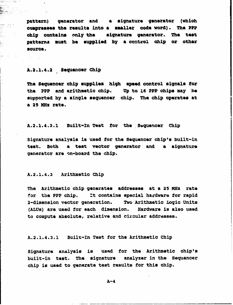
pattern) generator and a signature generator (vhich
compresses the results into a saaller code word). The PPP
chip contains only the signature generator. The teatpatterns must be supplied by a control chip or othersource.
A 2.1.4.2 Sequencer Chip
The Sequencer chip supplies high speed control signals forthe PPP and arithmetic chip. Up to 16 PPP chips may besupported by a single sequencer chip. The chip operates ata 25 MHz rate.
A.2.1.4.2.1 Built-In Test for the Swquencer Chip
Signature analysis is used for the Sequencer chip's built-intest. Both a test vector generator and a signaturegenerator are on-board the chip.
A.2.1.4.3 Arithmetic Chip
The Arithmetic chip generates addresses at a 25 MHz rate
for the PPP chip. "t contains special hardware for rapid2-dimension vector generation. Two Arithmetic Logic Units
(ALUs) are used for each dimension. Hardware is also usedto compute absolute, relative and circular addresses.
A.2.1.4.3.1 Built-In Test for the Arithmetic Chip
Signature analysis is used for the Arithmetic chip's
built-in test. The signature analyzer in the Sequencer
chip is used to generate test results for this chip.
A-4

lmoe of the dodu.Aes indicate how to tat the chipsetwhile it is in a systeat. Uhether the test data is read outover a dedi.ate line or over a bus was not indicated.
A. 2.2 Hughes Aircraft Coupany
A.2.2.1 The Chiplet
Chip Complexity Technology Status(No. Transistors)
Digital 72,000 CMOS/SOS FunctionalCorrelator
Algebraic Hncoder/Decoder 79, 000 Co08/SOS In Fab-
rication
Signal Tracking DesignSubsystea -60,000 CROS/808S omplete
10/84
Electro-Optical DesignSignal Proc. CMOS/SOS complete
8/84
Configurable GateArray -32,000 CMOS/SOS In Fab-
rication
A-5

The Hughes chipset is designed for a wide range of
communioations systems that operate in a high noise or
hiMzly jauumd environment. The Signal Processor and catearray are recent additions to the chip set and data is not
yet available for them.
A.2.2.3 Tachnolngy Insertion
The systems which havw been targated for the Hughes chip-
sat are a hybrid of the Position Location and Reporting
System k^PLRS) and the Joint Tactical Information
Distribution Location and Reporting Sys~ex (.7TIDS) called
the PLRS/JTIDS hybrid and a signal processor for *he F/A-
is.
The PLRS/JTIDS hybrid system will be able to operate in
both the PLRS and JTIDS environment6 though it may not beable to operate in all modes in both. The F/A-18 will use
Hughes designed parts fabricated by Fairchild.
A.2.2.4 The Chips
A.2.2.4.1 Digital Correlator
Th" digital correlator is a 129-stage by 4-bit correlator
cunfigured as fouX 32-stage by 4-bit sections. Each stagecorrelptes two bits of in-phase data and two bits of
quadrature-phala data with a single reference bit. By
proper scaling of the sections, the chip may be
reconfigured as a 64-stage by 8-bit correlator with each
stage correliting with four bits of in-phase and four bitsof quadrature-phase data. The length of each section may
be selected to be from 2 stages to 32 staqes in steps
A-$

of "adtm-phase data. fte length of each section maybe selected to be Mra 2 stages to 32 stages in steps
o2f . A nagnitude circuit is avAilabla at each sectionfor nonoherent correlation. A threshold circuit is
provided on each chip. The chips are configured by passing
data to internal control registers over the system commanddata-bus. CorrelatOr chips say be cascaded to torncorrolators with lengths of up to 10,912 stagas.
A.2.2.4.1.1 Built-In Test for the Correlator Chip
The correlator uses both set/scan and signcturs analysisfor its built-in test. Rech aorrelator section uses
signature analysis. The signal register is configured as a
32 *,-ge pattern generatcor and the reference register as a
32 bit signature analyzer. Initial patterns nay be loadedinto the pattern generator and signature analyzer over the
command databuc. The number of clocks in th^ test are
controlLed externally by a TEST pin input. Communications
between the sections on the chip and idditional circuitry
(such an the threshold detection circuit) are tested byset/scan. The input and output registers are linkedtogether as a long setscan chain. Data nay be input to
this chain over the system command databus. The data is
then processed (controlled by the TEST pin). Results are
read back through the command databus to the control
processor. In both tests, the control processor checks theresults against known good results. Faul- simulation
indicates a coverage of better than 95%.
A. 2.2.4.2 The Algebraic Encoder/Decrder Chip
¶ ho Encoder/Decoder chip possesses processing elements
capable of encoding and decoding all primitive binary
A-7

3Ssehudii-U e a (D) codes, including Reed
Solomn codes, up to length 64, with 32 data bits. Data
may be passed through the chip either by dedicated data
pins or the oumend databus. The eight-bit comnd flatabua
co. neots the chip to the oontrol processor ead is usedfor chip configuration and test commendo.
1.2.2.4.2.1 Built-In Test for the Algebraic Incoder/Deader Chip
All of the rzgisters on the chip, except for some of those
in the test cirouitxr, are included in one of 5 set/scanchains. The set/scan chains are loaded over the cnamand
databus by the controlling processor. The test is then
initiated by a command sent over the bus. On-board
circuits time the test. Status bits report results of
the test, The set/scan registers may also be read to
hel? isolate fam-lts. Fault coverag information was not
available.
A.2.2.4.3 Signal Tracking Subsystem Chip (STS)
This chip contains one tracking loop whicl nay ba
3onfigured for phase frequency or code tracking. Also, one
pseudo-randon noise (RN) sequence generator and a
code/sample clo., are on-board. Tvo or more chips are
required for me.st applications. The chips are programmable
to handle a wide range of signal tracking requirements.
A.2.2.4.3.1 Built-In Test for the Signal TrackingSubsystem Chip
Set/scan ari signature analysis are both used for the STS
chip. Tests are initiated by a control processor with
1-8

mds ever tho Qmautwl dauesm. "ItSu & a• rod by theoontrolling pri@@esor and omvazed to known good Meults.sault coverage information was not available.
A.2.2.4.4 Eleotro-Optical Signal Processor
This part was originall7 an in-house project. It was
recently picked up for support by the VISIC program. As a
result, no information waks available.
A.2. 2.4.5 Configurable Gate Array
This part was originally an in-house project. it was
recvaitly picked up for support by the VHSIC program. As a
result, no information was available in the documents
examined.
A. 2.2.5 System Test Procedure
These chips are designed to operate in a system which is
controlled by a microprocessor or other suart controller.
The same databus used to program the chips 'for a
particular configuration (which configuration may be
changed on-line) is used to control the testing of the
parts. The actual testing must be done ofti-line (that is,
during time periods when data is not beihg trantaitted orreceived). The testing is initiated by transmitting acoumand to put tha parts in the self test mode. At thistime their set/scan registers may be initialized for thetest. An externally supplied tiUinc signal is used tobegin the test process. At the end of the test, results
are read by the controlling processor and coxpared tostored values of the correct results.
A-9

A. 2. 3. 1 The Chipete
chip Compexity ftehnlo"gy Status
Complex Multiply 100Go O W=k ca alato deuivereld
to NoO
A.2.3.2 General
The I= ohireet conssist,• Of jast one part, the comtplexMlatiply a aoumalte (CtL) Chip. fte CM Chip am perfom100 million Mltiplication& per second. FCu 16 by 16multipliers With aomaators, GeLh With a !24-bit output,are available on chip for real or complex multiplicationand addition, 100 million real or 25 million complexoperations per second may be perormed. Bach subsection(containing i ultiplcktion and eWdition 01 -.cuitry)operates at ..2.t5 MIz real or 6.25 MUs complex rates.
A. 2. S. 3 Technology Insertion
The ayst•m which have been targeted for the ZIN chip are
he AN/UY8-1 soobuoy signal processor used on theLockheed P-3C and 8-3A aircraft and the XBM/Sikorsky Lamps1k *.3.
A-l0

ho2. 3.4 Built-nfl Test for the Complex Multiply andAocumulate Chip
Signature analysis using a level sensitive scan design andon-chip monitoring are used for built-in test. Parity bits
are available on all ch i p irierfaces. Adder overflow and
comparators for adjacent multipliers are also available.
The comparator nay be used when spare sections are
available in the application. Errors aze recorded in a 10-
bit register and one of three interrupt requests is
generated: one for parity errors (INTl), one for compare
errers (XnT2) and one for overflow errors (INT3). The chip
is stopped w, the detection of an error. All of the
latches on the chip are connected to torn 16 scan strings. A
20-bit pattern generator foeds all of the scan strings.
Rsults of the test are formed in a 16-bit signature
analys:a. This test has a fault coverage of over 90%.
A.2.3.3 System Test Procedures
Two types of testing are available on the chip, on-line
and off-line. The off-line test requires that the system
not be using the CA for calculations during the test
procedure. This is when the signature test is performed.
It is typically performad during power-up procedures, but
may also Lo performed periodically if the system
schedules periods during which health status is determined.
The on-line tests are performed during normal operation.
The inputs and outputs to the chip include parity bits.
Most 1/O failures eventually lead to parity failure. The
on-line test may be used when the system design results in
spare multiply and accumulate sections being available.
The results of adjacent sections arc compared. If they do
not match, the test has failed. Failure of any of the
above tests results in an interrupt request being
A-11

eNeated. •At that point it Is up to the Control processor
to take appropriate action.
A .24 %4=s ZintoWAents
A.2.4.1 "to Chipset
chip Camlexity Tachnoloqa Status(go. Transistors)
static UAN 440.000 Z110S Soaedeliveredto DOD
Wultipath Svwith 30,000 Bipolar Soedelivered
to DOD
Array Controllerf' 120,000 Bipolar UndeM r
Sequencer test
Vector Arithmetic 8,5000 Bipolar Under
L.Cgio Unit test
Vector Address 130,000 Bipolar Zn
Generator layout
Data Processor Unit 190,000 Bipolar In final
design
General Buffer Unit 130,000 Bipolar In finaldesign
Device Interface 190,000 Bipolar In final
design
A-12

A.2.4.2 General
Four of the seven thtps at* designed for us* in an arrayprocessor for high opeed signal processinq. The otherthree chips may be used in a standard 1750A type
processor.
A.2.4.3 Technology Insertion
The systems which have been targeted for the TexasInstruments chip set are a MIL-STD-1750A data processor,the launch and leave guided bomb, the Hellfire air tosurface missile guidance system, TOW-2 antitank missileguidance subsystem improvement, the Army LHX helicoptercentral processor, the Army M-i tank fire control systemprocessor and the Integrated Communication NavigationIdentification Avionics (ICNIA) program.
A.2.4.4 The Chips
A.2.4.4.1 Static RAM
The Static RAM is a 72 kilobit Random Arcess Memoryconfigured as an SK by 9 bit memory. It has a paritygenerator and checker built in. Ths ninth bit is theparity bit. It features write protection circuitry forblocks of 1K words and pipelined operations to improve
throughput.
A-13

A.2.4.4.1.1 Built-In Test for the Static RAM
The only built-in tort feature on the RAM chip is theparity generator/checker oircuitry.
A.2.4.4.2 Multipath Switch
The Multipath Switch contains a programmable crossbarmultiplexer capable of providing up to six one-way paths
between six 4-bit memory ports and six 4-bit processorports. Up to six independent bus-to-bus connections perclock cycle are possible.
A.2.4.4.2.1 Built-In Test for the Multipath Switch
On-chip self testing is provided using signature analysis.If a result disagrees with the predetermined fault-freesignature, an error bit is set. Fault coverage (excludingI/O circuitry) ts expected to exceed 99 percent.
A. 2.4.4.3 Array Controller/Sequencer (AC/S)
The AC/S chip provides microprogram addresses for 64Kwords of external memory or 2K words of internal mask-programmable RON. It operates at a 25 MH% rate. Capabilityfor sequential addressing, conditional or unconditionalbranching and subroutine call linking and return through a16-deep stack are provided.
A-14

A.2.4.4.3.1 Built-In Test for the Array Controller/
Sequencer Chip
On-Chip self testing in tx,ý~jV'idd using signature analysis.If a rsult isTa: with the predetermined fault-free
sign~~iq~zirefan error bit is set. A microcode test checks
1instructions and all of the AC/S functions. This test
is also compressed using signature analysis. Faultcoverage (excluding I/O circuitry) is expected to exceed
99 percent.
A.2.4.4.4 The Vector Arithuetic Loqic Unit (VALU)
The VALU is a high performance computation unit optimized
for signal processing applications. It forms part of a
configurable arithmetic pipeline which includes a 16 by 16
multiplier, a 44-bit adder/subtracter and a 16-bit fullcapability arithmetic logic unit. It uses an external RONmicrocode, making modifications to the code structure
straight forward. While it does not perform floating pointoperations, it supports them with'9 opcodes.
A.2.4.4.4.1 Built-In Test for the Vector Arithmetic
Logic Unit
On-chip self testing is provided using signature analysis.
If a result disagrees with the predetermined fault-freesignature, an error bit is set. Fault coverage (excluding
I/O circuitry) is expected to exceed 99 percent.
A-15

A.2.4.4.5 Vector Address Generator (VAG) Chip
The VAG chip is a high speed, 16-bit address generator
which is optimized for use with highly regular data
structures such as arrays. A full 16-bit ALU (ArithmeticLogic Unit) is provided for calculations including
addresses and other operands. It can handle sequential
addressing, bit reversed addressing (for Fast FourierTransforms (FFT)), indexed addressing and data directed
addressing.
A.2.4.4.5.1 Built-In Test for the Vector AddressGenerator
On-chip self testing is provided using signature analysis.
If a result disagrees with the predetermined fault-free
signature, an error bit is set. Fault coverage (excludingI/O circuitry) is expected to exceed 99 percent. This test
requires 6250 clocks or one fourth of a millisecond torun.
A.2.4.4.6 Data Processor Unit (DPU)
The Data Processor Unit is a general p'rpose
microprocessor for the 1750A instruction set. It operates
at speeds to 25 MHz with a maximum throughput at 25 MHz
predicted to be two to four MIPS with the DIAS mix. It canperform a register to register add in 40 nanoseconds and a
16-bit multiply in 440 nanoseconds. It has three
programmable timers.
A-16

A.24.4.6.l Built-In Tast for the Data Proc*osor Unit
On-chip self testing is provided using signature analysis.if a result disagrees with the predetermined fault-freesignature, an error bit is set. Fault coverage (excludingI/O circuitry) is expected to exceed 99 percent.
A.2.4.4.7 General Buffer Unit (GBU)
The GBU is a bus coupler used between the memory bus(MBUS) and the system bus (SBUS).
A.2.4.4.7.1 Built-In Test for the General Buffer Unit
On-chip self testing is provided using signature analysis.If a result disagrees vith the predetermined fault-freesignature, an error bit is set. Fault coverage (excludingI/O circuitry) is expected to exceed 99 percent.
A.2.4.4.8 Device Interface Unit (DIU)
The DIU is a general purpose microprocessor for use as acoprocessor with the DPU. It implements I/O, DMA andremote multiprocessing operations. It operates at speeds to25 MHz and has 16 interrupt levels. It is the same circuitas the DPU but uses a different microcode.
A.2.4.4.8.1 Built-In Test for the Device Interface Unit
On-chip self testing is provided using signature analysis.If a result disagrees with the predetermined fault-freesignature, an error bit is set. Fault coverage (excludingI/O circuitry) is expected to exceed 99 percent.
A-17
A. 2.4.3 System Test Procedures
Tests for these chips are controlled by sending commands
ovar ths system maintenance bus. The signature analysis
tests must be performed off-line. The test results may be
read over the system maintenance bus. If the chipset is
configured as the system main processor, testing is
controlled by the Data Processor Unit. Periodic testing
requires the availability of time segments during which
the processor may be freed from normal duties. All chips
report via the system maintenance bus to the DPU which
stores the system health information in a status register.
It is the responsibility of the DPU to act upon that
information.
Testing may also be initiated by a separate processor over
the system maintenance bus.
Fault simulations have not yet been performed to verify
the high fault coverage predictions.
A.2.5 TRW/Motorola
A.2.5.1 The Chipset
Chip Complexity Technology Status(No. Trcnsistors)
WindowlAddressable 58,000 Bipolar Functional
memory
Content Addressable 66,000 Bipolar Functional
memory
A-18

atriax switch 13,SO0 Bipolar ?nmotional
Pmtr voret Naery 600 000 eweU Funftienal
xualtiplior/ 42,000 Bipolar Under TestAoouaulator
Microcontroller 25,000 Bipolar In Fab-rication
Register Arithmetic 36,000 Bipolar In Fab-Logic Unit rication
Address 6enerator 34#000 Bipolar In Fab-rication
Convolutional 73,000 Bipolar In DesignDecoder
Convolver 74,000 CMOS In Fab-rication
Fast Fouriar 50,000 CMOS LayoutTransform Arithmetic CompleteUnit
FFlT Control Unit 60,000 CMOS In Design
Configurable Gate 26,000 CMOS In DesignArray
A 2.Z.2 General
The TRW/Motorola chip set is designed for use inelectronic warfare And extrerily high frequency satellitecomMunications.
A-19

A.2*.53 TechnolOff Insertion
Thb systems which have been taTgeted for the TRW/Motorola
chipset are a pr grammable signal processor for ICNIA, agen6ral purpose programmable signal processor, the A•I/AO-
131 airborne jauser pod improvement progrru, INWS
(integrated Electronic Warfare System) and a next
generation military satellite.
A.2.5.4 The Chips
A.2.5.4.1 Window Addressable Memory (WAX)
The WAX chip allows incomin, da-ta to be examined through
eight different adjustable "windows" simultaneously to
determine if certain variables fall in the range of valuesviewed through the windows. It provides an eight-way
sorting action.
A.2.5.4.1.1 Built-In Test for the WAX
Information on the WAX was not included in the chip'sspecification document.
A.2.5.4.2 Content Addressable Memory (CAM)
CAM allows a string ^f input data bits, called a vecto!-,..o be oompa',ed with previously stored data. A vector maebe divided into fields, permitting searches for Patchis in anumber of ways.
A-20

A.2.3.4.2.1 Built-Zn Test for the Content Addresbable
Memoy
Set/scan is provided through a aiintenance natwork nods.
Data is loaded into the chip, which may then be single
stopped. The resulting data is then read out to see if it
was correctly processed. Information on the mairtanance
network node is included in section A.2.5.5.
A.2.5.4.3 Matrix Sw4 .tch
The Matrix Switch is an eight-input eight-output 4-deepcrossbar switch capable of operating at 25 MHz. Iv
switches rescurcos and data between memories, arithmeticunits, the address generator, etc.
A.2.5.4.3.1 Built-In test for the Matrix Switch
Set/scan is provided through a maintenance network node.Data is loaded into the chip, which may then be oinglestepped. The resulting data is then read oui to seR if itwas correctly processed. Information on the maintenancenetwork node is included in section A.2.5.5.
A.2.5.4.4 Fcur Port Remory
The Four Port Memory is designed to read two independentaddresses and write two indepondent addr3sseS each clock
cycle. t is configured as 1024 4-bit words withpipelining and both synchronous and asynchronous modes of
oparation.
A-21
A. 2.5.4.4.1 Built-In Test for the Four Port Namory
Set/*csn is provided through a Maintenanoe network node.Data is loaded iuto the thip, which aiy then be singlestepped. The reaau7ti• data is then read out t see if itwas oorrectly prodsased. Znformation on tUs ainteranotnetwork node is in~ln.u4d in section .*.2s.t;.
A.2.5.4.1 Multiplier/Acaunlator (M&C)
The XkC chip computea sems of prodvats and accusulatea
interaediate data.
A. 2..S.4.S.l l.ilt-In Teat- fo the :-tltiplier Accumulator
Set/scan is provid-1"d through a maintenance network node.
Data ts loaded into t•he Cihip which nay then be single
stepped. The resulting data is then read out to see if it
was correctly processed. Information on the maintanance
neuvork node in includeti in section A.2.5.5.
A.2.5•4.6 ticroconztroller
The microcontroler pro-iidas microinstruction sequencing
control. St generates a Itt-bit addroess.
A, 2.3.4.C.1 3uilt-In Test for the Micvocoratroller
Set/scan is provided through a maintenance network node.
Data is loaded into the chip, Vwiti may then be single
stepped. The resulting data is then read out to see if it
was correctly processed. Information on the maintenance
network zi•de is included in section A.2.S.5
A-22

A1250.4.01 Penieter Ataetio Zagio Unit (•&U)
Te P" implleamints 16-bit .trithuetia am boolsan
mfltilons. Im~la chip double precision is supported.tittichip nultiple precision is tupported (with loss of
speed trou the 25 Mm iingle chip operation). The chip
contains faIL-ares which fazilitatc fi 3,ting point
operatiWAS.
A,2,5,4,?,l ftilt"Zn Test for the Register Arith-emti
Logic Unit
setiscan is provided through a aaintenance network node.
Data is loaded into =aa chips which may then be s.tngle
st*Vped. The resulting data is then read out to see if it
was cormectly processed. ITforatoaion on the na.antenance
netvork nude is inal,.ded in section A.2,S.5.
A.j.35.4.8 Addrmss Ge•erator (AG)
The AG chip is a slave procersor vLch generates seqvences
of 1c-bit addresses (erne address in each clock cycle) for
quick aocess to data strdctures.
A.2.5.4.8.1 D.Alt-In Test for the Address Wmeeator
Set/scan is provided through a naintenance netvork node.
Data !.s loaded into the chip, which may then be sirtjle
stepped. The resultinC data is then read out to see if it
was ccr• ctlY processed. Information on the mainte.ince
network node is inuluded in section A.2,5.5.
A-23

L2.5. .4 • Cioivolutional Deooder
Snotion on the Uonvolutiomal DOGOe was not includedin the imipo qpGetfioation.
A.i.5.4.0 •Convolver
Intozation on the Coaolver vas not iwluded in the Chipsspoiltoatiea.
&.2.S Ll.•I Fast Fyouier Transform Arithsetic Unit
ZntrMation on the Fast Pouarier Trausfo= Arithmetic Unitwas not incluiad in the chips specitication.
A.2..4..12 FIT Control Unit
Inforuatior, on the FFT Control Unit was not included in
the chips specification.
A.2.5.4.13 Configurable Gate Array
Informution on the Configurable Gate Array was not
inoluded in the chips specification.
A 2.5 * 5 System Tet Procedure
Bact chip has a aaintenance network node (100N). The
purpose of the node is to extract command information and
data from a serial inpuc atream and initiate a response to
that command. All of the registers and flip-flops on each
chip, except those in ths MRI itself. are confiqurable for
A-24

-1aulten na a setema leog ush may be laded trM them f t* e s" is Pwi: dw nwo vlthot altering the
ofthe dw#. fiten= testA Met ooutte the a7 ~nOdle Ot the @UP ip th the 'q Me Mawma etreom ed be
able to intexs ths xemal ebt e fm any test,
S•00 ips4
Chit Ownlexity Tethholoqy Status
static my- 't0.D04) OMS 4Q64
Pipeline Arithmetic 133,0O0 CMOs 1Q85unit
lxtended Arithmetli 92,000 CM6 1Q65unit mualtiplier
General Purpose 7?,090 CMOS 1Q85Controller
10,000 gate Gate 40,000 CMOs QArray
Mnhanced Extended Not Avail. CMO Deferred
Arithmetic Unit
A.2.6.2 General
The chipset performs 5 functions: 1) Complex number
arithmetic vector processing, 2) Vector-scalar
A-25

pteesing, 3) 7E1oatin'7 Point data pwoeesing, 4)eRLrehsal uAlti•reOessor systea control am 5)
kwide bulk mmory.
A. I2 - .3 TechnTolgy Iaeti•on
nhe systems which have been targeted for theW1est•i•hmou/letional C"Nipsat are an airborne AlAM1 signalPflOSSOZ, an elitW.umOtio tsignal - Lat the X-i
taAk, air defenue RDAIM fire Contr.o, ystant the avionicssuite for the uRX helicopter the UrAF/toeing 1-3A PADR,an a0danced power aawag1eat systea for electronicWarfare, a MZL-STOD-1750A general purpose coMputer, atactical air control center and an advanc*d programmablesignal processor for retrofit into AMG-68 PADAR used inthe General Dynamics 1-16.
A.3.6.4 The Chips
A.Z.6.4.1 The static RAM
The 64K-bit static RAN is configured as OR words of 8bits. It feafurea a 25 nanosecond access/cycle time.
A.2.6.4.1.1 Built-In Test for the SR by 8-bi.t Static RAN
No built-in test provisions are provided.
A.2.6.4. Pipeline Arit-metic Unit (PAU)
The PAU perforas high speed veotor-efficiezt operations.
Sase of the possible functions performed are FiT,
A- .26

recursive filtering, tranoversal filtiring, matchedfiltering, convolutional filtering, spectrum shifting,
weighting &nd band limited interpolation.
A.2.6.4.2.1 Built-In Test tor the Pipelined ArithmeticUnit
The chip is divided into test cells of up to 5000
equivalent gates. Lach test cell has test registers at all
of its inputs and outputs. A special test bu& (TBUS) is
used to control testing. Simulation information was not
available.
A.2.6.4.3 The Extended Arithmetic Unit Multiplier
The Extended Arithmetic Unit Wiltiplier provides highspeed fixed end floating point multiply and divide
operations. It uses MIL-STD-1750A formats and can also
handle the Westinghouse 64-bit floating point format.
Pipelining provides the capability of providing a resultevery 40 nanoseconds.
A.2.6.4.3.1 Built-In Test for thu Pipelined Arithmetic
Unit
The chip is divided into test cells of up to 5000
equivalent gates. Each test cell has test register3 at all
of its inputs and outputs. A special test bus (TBUS) is
used to control testing. Simulation information was not
available.
A-27

A.2.6.4.4 The General Purpose Controller
The General Purpose Controller is intended to be used as'
the microprogrammed control element within a signalprocessor, embedded processor or general purpose
processor. It addresses up to 262K words (16 bits perword) of memory. It features a 40 nanosecond cycle (25
MHz) and has a design goal of 3 million instructions persecond (NIPS), Digital Avionics Instruction Set (DAIS)
mix, for a MIL-STD-1750A computer configuration.
A.2.6.4.4.1 Built-In Test for the General PurposeController
The chip is divided into test cells of up to 5000equivalent gates. Each test cell has test registers at allof its inputs and outputs. A specii) test bus (TBUS) is
used to control testing. Simulation information was notavailable.
A.2.6.4.5 The Gate Array
The gate array contains the functional equivalent of 7,904
',\•2-input NAND gates. It has 160 bonding pads and 46 input,
output and 76 bidirectional buffers.
A.2.6.4.3.1 Built-In Test for the Gate Array
The entire gate array i treated as a single test cell.
All of the inputs and outputs pass through test registers
which may be controlled by the test circuitry. A special
test bus (TBUS)" is used to control testing.
A-28

A.2.6.4.6 Tha Enhanced Extended Arithmetic Unit
The Enhanced Extended Arithmetic Unit provides a 16-bit
multiply with a 32-bit product, 32-bit floating point
addition and subtraction in 3 clock cycles (including
denormalization and normalization), and provides support
for arithmetic operations on 32-bit integers and 48-bit
floating point values. A 16-bit add/subtract is performed
in 1 clock cycle. A 32 deep 16-bit stack is available.
Features are available to facilitate double precision (64-bit) floating point, single and double precision complex
operations and floating complex operations.
A.2.6.4.6.1 Built-In Test fdii the Enhanced Extended
Arithmetic Unit
The chip is divided into test cells of up to 5000
equivalent gates. Each test cell has test registers at all
of its inputs and outputs. A special test bus (TBUS) is
used to control testing. Simulation information was not
available.
A.2.6.5 System Test Procedures
Each chip in the chipset (except for the RAM) has an on-board BIT controller microcell which controls all testing
within the chip. It operates on commands and data it
receives over the test bus (TBUS). BIT controllers on
separate chips within a system will test the connections
and I/O buffers in paths between the chilis.
The processor controlling the test bus depends upon the
system design. It would appear that this system would have
difficulty fully testing itself. A separate test
processor may theregore be necessary.
A-29

/ A.3 CONCLUSIONS
The schedules for the VHSIC Phase I contractors indicate a
deadline for the operational brassboards at the end of
1985. Delivery of 100 parts of each chip in the chipset
are also due at that time. However, there are concernsthat the yields will be so low that some parts may cost as
mueh as $5,000. To combat this, the program office
recently funded yield enhancement programs to each
contractor. These programs cost a total of $15 million for a
32 month effort. This would seem to indicate that parts in
reasonable quantities will not be available until mid 1987.
However, all of the chip specifications should be stable
enough for design purposes by mid 1985, and parts may be
available in small quantities by the end of 1985. What does
the VHSIC program buy us? The Rughes VHSIC digital
correlator replaces a 32-stage, 5 MHz part which uses
analog summing that has limited cascadability. This
correlator also performs the magnitude calculations and
threshold detection that previously were done off-chip. It
offers five times the processing power and four times the
speed of the part it replaces. It also may be configured
for a wider variety of applications, including very long
correlations. Four times faster at one fifth of the area
means the part has 20 times the capability of current
parts.
The VHSIC program has stressed making the parts general
purpose. Various applications will not use all of the
features on a chip. The end result of this is that some of
the possible processing gain is lost. However, another
goal of the program was to make general purpose VHSIC
A-30

mo lls available which may be used in new chip
designs. these ohipm may be made more special purpose and
use only these cells which are needed. Chip design tools
developed on the VNS!C prog"ra will simplify the design
of those semicustom parts.
A-31

APPENDIX B
IIAMMNG CODES DESCRIPTION
Hamming codes are a class of generalized parity check codes
usually used for single error correction. They can also
provide a greater level of error detection than a standard
parity check code and additional levels of error correction,
at added hardware cost, Assume that there are q information
bits which we want to protect with a Hamming code. In this
case, c check bits must be added where c is determined by thecondition that:
c2 > q + c +
The result is a (q + c] - bit word. The check bits are placedin the word so that error correction is easy to do. That is,if the [q + c] - bit word is given by:,
b b bb bq+c q+c-l... 3 2 1
the3 the c check bits are placed in the positions Bi, where i- 2 for J-O, 1, 2, , . ., c-l. The values of the bits are
determined such that they insure that the parity sum equals 0for error free words. There are two steps to defining the
parity equations.
Step One: Integer Sets
Define P to be the collection of integers whose binaryrepresentation has:
a. c or fewer bitsb. The J-th bit equal to 1
B-1

Construct these sets for J-i to c.
Stop Twot Parity Equations
The parity sums are then defined by:
r- Zb for kEPC , k < q + c
where the c equations ure given for, Jul., . .. , c. The value
of thl bcheak bit in selected so that the parity equation r -0is satisfied for Jul, ... , c. This gives a unique result
since each of the parity suns contains exactly one of the
check bits and no check bit eppears in more than on3 parity
sun.m3rea
If wa are given 4 information bits, then q - 4 and c must be
3 so the code word contains 7 bits with the check bits at
locations b , b , and b 4 The three integer sets are givenby:
P, M (1, 3, 5, 7)
P 2- (2, 3, 6, 7)2
P - (4, 5, 6, 7)3
The three parity equations become:
1. b + b + b + b -01 3 5 7
2 3 6 7
3. b + b + b + b - 04 5 6 7
B-2

Vhere + is mod 2 Lddition.
Nov, to sed the information bits 1 0 0 1, the three paritybits are selected to that equations 1-3 are true. Thus b1 - 0b2 - 0 and b4 al. The transmitted word is 1 0 0 1 1 0 0.Suppose an error owoirs and the word becomes 1 0 0 1 1 0 1
(that Is, b becomes a 1). Evaluating the three parity sumsS 1in reverse ordar on the faulty word gives the result:
r -1+0+0+1-03
r -0+1+0+1-0
r -1+1+0+1-11
The binary output of the parity sum is 001 or decimal 1-'which
correctly identifies b as the f&ulty bit.1
B-3