istanbul technical university graduate school of...
TRANSCRIPT

Department of Mechanical Engineering
System Dynamics and Control Programme
Anabilim Dalı : Herhangi Mühendislik, Bilim
Programı : Herhangi Program
ISTANBUL TECHNICAL UNIVERSITY GRADUATE SCHOOL OF SCIENCE
ENGINEERING AND TECHNOLOGY
M.Sc. THESIS
JANUARY 2013
POSITION AND SPEED CONTROL OF SHAPE MEMORY ALLOYS
FOR USAGE AS ACTUATORS
Gökçe Burak TAĞLIOĞLU


JANUARY 2013
ISTANBUL TECHNICAL UNIVERSITY GRADUATE SCHOOL OF SCIENCE
ENGINEERING AND TECHNOLOGY
POSITION AND SPEED CONTROL OF SHAPE MEMORY ALLOYS
FOR USAGE AS ACTUATORS
M.Sc. THESIS
Gökçe Burak TAĞLIOĞLU
(503091631)
Department of Mechanical Engineering
System Dynamics and Control Programme
Anabilim Dalı : Herhangi Mühendislik, Bilim
Programı : Herhangi Program
Thesis Advisor: Prof. Dr. Şeniz ERTUĞRUL


OCAK 2013
İSTANBUL TEKNİK ÜNİVERSİTESİ FEN BİLİMLERİ ENSTİTÜSÜ
ŞEKİL HAFIZALI ALAŞIMLARIN EYLEYİCİ OLARAK
KULLANILABİLMELERİ İÇİN KONUM VE HIZ KONTROLÜ
YÜKSEK LİSANS TEZİ
Gökçe Burak TAĞLIOĞLU
(503091631)
Makine Mühendisliği Anabilim Dalı
Sistem Dinamiği ve Kontrol Programı
Anabilim Dalı : Herhangi Mühendislik, Bilim
Programı : Herhangi Program
Tez Danışmanı: Prof. Dr. Şeniz ERTUĞRUL


v
Thesis Advisor : Prof. Dr. Şeniz ERTUĞRUL ..............................
İstanbul Technical University
Gökçe Burak Tağlıoğlu, a M.Sc. student of ITU Graduate School of Science
Engineering and Technology student ID 503091631, successfully defended the
thesis entitled “POSITION AND SPEED CONTROL OF SHAPE MEMORY
ALLOYS FOR USAGE AS ACTUATORS”, which he prepared after fulfilling the
requirements specified in the associated legislations, before the jury whose signatures
are below.
Date of Submission : 17 December 2012
Date of Defense : 18 January 2013
Jury Members : Doç. Dr. Müştak YALÇIN .............................
İstanbul Technical University
Y. Doç. Dr. Murat TABANLI ..............................
İstanbul Technical University

vi

vii
To the penguins trying to survive on distant lands,

viii

ix
FOREWORD
In this project, which is funded by the BAP unit of ITU, the characteristics of shape
memory wires are examined and a proper method for controlling the position and
speed of the shape memory wires is searched.
I would like to thank my instructor Prof. Dr. Şeniz Ertuğrul who enlightens me with
her deep knowledge and guidance; and the BAP unit of ITU for funding this project.
I also want to thank to my friend and co-worker Research Assistant Cihat Bora Yiğit
for his continuous support and Technician İbrahim Akın for his help in the
production of the mechanical parts.
December 2012
Gökçe Burak TAĞLIOĞLU
(Mechanical Engineer)

x
xi
TABLE OF CONTENTS
Page
FOREWORD ............................................................................................................. ix TABLE OF CONTENTS .......................................................................................... xi
ABBREVIATIONS ................................................................................................. xiii LIST OF TABLES ................................................................................................... xv LIST OF FIGURES ............................................................................................... xvii
SUMMARY ............................................................................................................. xix ÖZET ...................................................................................................................... xxiii 1. INTRODUCTION .................................................................................................. 1
1.1 Shape Memory Alloys ........................................................................................ 1 1.2 Purpose of Thesis ............................................................................................... 4
1.3 Organization of Thesis ....................................................................................... 5
2. EXPERIMENTAL SETUP ................................................................................... 7 2.1 Overview of the Experimental Setup ................................................................. 7 2.2 Design of the Electronic Hardware .................................................................... 9
2.2.1 Overview of the electronic hardware .......................................................... 9 2.2.2 SMA wire driver ....................................................................................... 10
2.2.2.1 Design approach ................................................................................. 10
2.2.2.2 High KP controller .............................................................................. 13 2.2.2.3 Pure integrator controller ................................................................... 16
2.2.3 Voltage limiter .......................................................................................... 20 2.2.4 Main Board ............................................................................................... 22
2.2.4.1 Design approach ................................................................................. 22 2.2.4.2 Development environment ................................................................. 24
2.2.4.3 Implementation of analog outputs ...................................................... 25 2.2.4.4 MAX232 sub-board ........................................................................... 26 2.2.4.5 Software in PIC18F2520 .................................................................... 26
Initialization routines ................................................................................. 27 Main interrupt service routine .................................................................... 28 Low level serial communication routines .................................................. 29 High level serial communication protocol routines ................................... 30
Endless main loop ...................................................................................... 34 2.3 Design of the Desktop Computer Software ...................................................... 37
2.3.1 Design approach ........................................................................................ 37 2.3.2 Development environment ........................................................................ 37 2.3.3 Thread based structure .............................................................................. 40
2.3.4 Object based structure ............................................................................... 41
3. EXPERIMENTS .................................................................................................. 47 3.1 Open Loop Tests .............................................................................................. 47
3.1.1 Effects of averaging filter ......................................................................... 48 3.1.2 Current - position relation ......................................................................... 49
xii
3.1.3 Position - resistance relation ..................................................................... 50 3.2 Closed Loop Tests and PID Controller Tuning ................................................ 51
3.2.1 Tuning by Ziegler - Nichols method ......................................................... 52 3.2.2 Manual tuning ........................................................................................... 58
3.2.3 Modification on integral term ................................................................... 60 3.3 Frequency Response Tests ............................................................................... 64 3.4 Obstacle Detection Tests .................................................................................. 69
4. CONCLUSIONS AND RECOMMENDATIONS ............................................. 73 4.1 Results and Comments ..................................................................................... 73
4.2 Recommendations for Further Study................................................................ 75
REFERENCES ......................................................................................................... 77 APPENDICES .......................................................................................................... 79
APPENDIX A ........................................................................................................ 80 APPENDIX B ......................................................................................................... 81 APPENDIX C ......................................................................................................... 84 APPENDIX D ........................................................................................................ 86
CURRICULUM VITAE .......................................................................................... 87

xiii
ABBREVIATIONS
ADC : Analog to Digital Converter
Bps : Bits Per Second
DAC : Digital to Analog Converter
DAQ : Data Acquisition
DIP : Dual Inline Package
DOF : Degree Of Freedom
EDA : Electronic Design Automation
EEPROM : Electrically Erasable Programmable Read Only Memory
GCC : GNU Compiler Collection
GNU : GNU’s Not Unix
GUI : Graphical User Interface
I/O : Input / Output
I2C : Inter-Integrated Circuit
IC : Integrated Circuit
IDE : Integrated Development Environment
LED : Light-Emitting Diode
LVDT : Linear Variable Differential Transformer
MIPS : Million Instructions Per Second
MOSFET : Metal Oxide Semiconductor Field Effect Transistor
Op-amp : Operational Amplifier
PCB : Printed Circuit Board
PCI : Peripheral Component Interconnect
PIC : Peripheral Interface Controller
PID : Proportional Integral Derivative
PWM : Pulse Width Modulation
ROS : Robot Operating System
SMA : Shape Memory Alloy
SME : Shape Memory Effect
SPI : Serial Peripheral Interface
SRAM : Static Random Access Memory
Trimpot : Trimmer Potentiometer
TTL : Transistor-Transistor Logic
TUI : Text-based User Interface
USART : Universal Synchronous Asynchronous Receiver Transmitter
USB : Universal Serial Bus

xiv

xv
LIST OF TABLES
Page
Table 3.1 : PID coefficients calculated for 400 - 800 interval. ................................. 53 Table 3.2 : PID coefficients calculated for 550 - 650 interval. ................................. 56
Table 3.3 : Bandwidths of SMA wires in different operating zones. ........................ 68
Table D.1 : Properties of Nitinol wires [29]. ............................................................ 86

xvi
xvii
LIST OF FIGURES
Page
Figure 1.1 : Types of actuators: One-way (a), biased (b), two-way (c) [4]. ............... 2 Figure 1.2 : Shape memory effect [5]. ........................................................................ 2
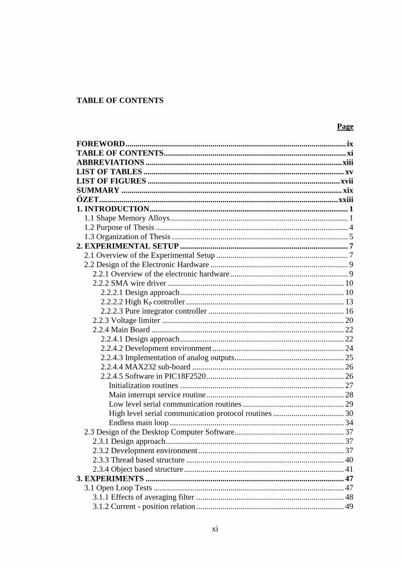
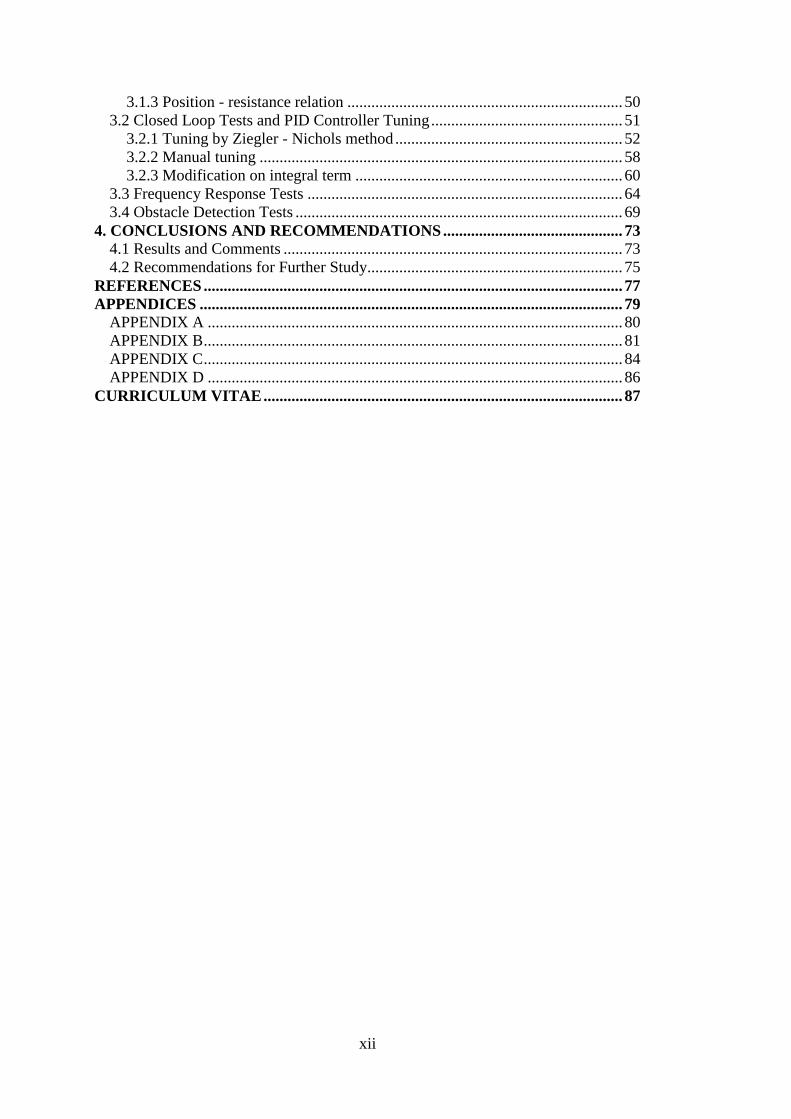
Figure 2.1 : Overview of the experimental setup. ....................................................... 7 Figure 2.2 : Relations between the components of the experimental setup. ............... 8 Figure 2.3 : Overview of the electronic hardware. ..................................................... 9 Figure 2.4 : Basic current controller circuit [21]. ..................................................... 13
Figure 2.5 : Schematic of the SMA driver circuit. .................................................... 14 Figure 2.6 : Step response of current of SMA driver. ............................................... 15 Figure 2.7 : Resistance value during the step response of SMA driver. ................... 15 Figure 2.8 : Schematic of the integral controlled SMA driver.................................. 17
Figure 2.9 : Step response of current of the new SMA driver. ................................. 18 Figure 2.10 : Resistance value during the step response of SMA driver. ................. 18
Figure 2.11 : High KI causing oscillations. ............................................................... 18 Figure 2.12 : Frequency response of SMA driver at 1 kHz. ..................................... 19
Figure 2.13 : Frequency response of SMA driver at 10 kHz. ................................... 19 Figure 2.14 : Schematic of the voltage limiter. ......................................................... 21 Figure 2.15 : Response of the voltage limiter. .......................................................... 21
Figure 2.16 : MCP4922 timing diagram [25]. .......................................................... 25 Figure 2.17 : Schematic of the MAX232 board. ....................................................... 26
Figure 2.18 : Flowchart of main interrupt service routine. ....................................... 29 Figure 2.19 : Data package formats. ......................................................................... 32 Figure 2.20 : Flowchart of the receive protocol. ....................................................... 33 Figure 2.21 : Flowchart of the main loop.................................................................. 36
Figure 2.22 : Class diagram. ..................................................................................... 41
Figure 3.1 : GUI of the open loop controller. ........................................................... 48 Figure 3.2 : Position - time - resistance graph (Unfiltered). ..................................... 48
Figure 3.3 : Position - time - resistance graph (Filtered). ......................................... 49 Figure 3.4 : Current and position graph of open loop controller. ............................. 50 Figure 3.5 : Current - position relation of the open loop controller. ......................... 50 Figure 3.6 : Position - resistance relation of the open loop controller. ..................... 51
Figure 3.7 : GUI of the closed loop controller. ......................................................... 52 Figure 3.8 : Determination of KCR in 400 - 800 interval........................................... 52 Figure 3.9 : Determination of PCR in 400 - 800 interval. .......................................... 53 Figure 3.10 : Response of PI controller (tuned in 400 - 800 interval). ..................... 54 Figure 3.11 : Response of PID controller (tuned in 400 - 800 interval). .................. 54
Figure 3.12 : Determination of KCR in 550 - 650 interval......................................... 55 Figure 3.13 : Determination of PCR in 550 - 650 interval. ........................................ 55 Figure 3.14 : Response of PI controller (tuned in 550 - 650 interval). ..................... 56
Figure 3.15 : Response of PID controller (tuned in 550 - 650 interval). .................. 57
xviii
Figure 3.16 : Sine and triangle response of PID controller (tuned in 550 - 650
interval). ............................................................................................... 57 Figure 3.17 : Sine wave response (KP = 10, KI = 10, KD = 0.2). .............................. 58 Figure 3.18 : Sine wave response (KP = 5, KI = 10, KD = 0.2). ................................ 58
Figure 3.19 : Step response (KP = 5, KI = 10, KD = 0.2). .......................................... 59 Figure 3.20 : Step response (KP = 5, KI = 20, KD = 0.2). .......................................... 59 Figure 3.21 : Sine wave response (KP = 5, KI = 20, KD = 0.2). ................................ 60 Figure 3.22 : Step response (KP = 5, KI = 10, KD = 0.2, modified I). ....................... 61 Figure 3.23 : Step response (KP = 12, KI = 64.9, KD = 0.6, modified I). .................. 62
Figure 3.24 : Step response (KP = 5, KI = 45, KD = 0.2, modified I). ....................... 63 Figure 3.25 : Sine and triangle response (KP = 5, KI = 45, KD = 0.2, modified I). ... 63 Figure 3.26 : Step response of the thick (0.15 mm) wire. ......................................... 63
Figure 3.27 : GUI of the frequency test. ................................................................... 64 Figure 3.28 : Bode plot of 0.076 mm wire in 400 - 800 interval. ............................. 65 Figure 3.29 : Bode plot of 0.076 mm wire in 500 - 700 interval. ............................. 66 Figure 3.30 : Bode plot of 0.076 mm wire in 550 - 650 interval. ............................. 66
Figure 3.31 : Bode plot of 0.15 mm wire in 400 - 800 interval. ............................... 67 Figure 3.32 : Bode plot of 0.15 mm wire in 500 - 700 interval. ............................... 67 Figure 3.33 : Bode plot of 0.15 mm wire in 550 - 650 interval. ............................... 68 Figure 3.34 : Photo of the obstacle. ........................................................................... 69
Figure 3.35 : Close-up photo of the (a) tight and (b) loosen SMA wire. .................. 70 Figure 3.36 : Position - resistance - time graph with introduced obstacle. ............... 70
Figure 3.37 : Position - time graph with introduced obstacle. .................................. 71 Figure 3.38 : Effect of obstacle on resistance with triangle reference. ..................... 71
Figure 3.39 : Effect of obstacle on resistance with step reference. ........................... 71 Figure 3.40 : Slope of position - reference curve with triangle reference. ................ 72
Figure 3.41 : Slope of position - reference curve with step reference. ..................... 72
Figure B.1 : PCB design of the failed SMA driver. .................................................. 81 Figure B.2 : PCB design of the integral controlled SMA driver. .............................. 81
Figure B.3 : PCB design of the voltage limiter. ........................................................ 82 Figure B.4 : PCB design of the MAX232 board. ...................................................... 82
Figure B.5 : PCB design of the DAQ card. ............................................................... 83
Figure C.1 : Screeshot of the MPLAB X IDE. ......................................................... 84 Figure C.2 : Screenshot of the Code::Blocks IDE. ................................................... 84
Figure C.3 : Screenshot of the wxFormBuilder. ....................................................... 85

xix
POSITION AND SPEED CONTROL OF SHAPE MEMORY ALLOYS FOR
USAGE AS ACTUATORS
SUMMARY
Shape memory alloys (SMA) are the materials that can return their previous shape
when a heat process is applied. They can be one of two phases: Austenite or
martensite. The temperature of the material determines the phase ratio. When the
material is cold, it is in martensite phase. Forces applied on the material at this stage
cause plastic deformation and shape change. When the material is heated, it
experiences a phase change towards the austenite phase and it returns to its previous
undeformed shape. This behavior can be utilized to build actuators.
Shape memory alloys draw attention mainly because of their high power to mass
ratio. Today, one of the biggest problems in robotics is the high mass and volume of
the classical actuators, compared to their power. For example, a noticeable part of the
total mass of a robotic arm is the mass of the electrical motors themselves. Shape
memory alloys on the other hand, can generate high forces even though they have
low mass. However, their temperature dependent and hysteretic behavior makes
them harder to control.
In this study, an experimental setup allowing experiments on the shape memory
alloys is built. The main goal of this study is to develop an SMA actuator system that
can replace the conventional electric motors used in robotic applications. In this
concern, various experiments are performed and results are obtained on the
experimental setup.
The experimental setup consists of mainly 3 parts: Mechanical, electronical and
software. The mechanical part consists of a test load that is fixed on a linear guide
positioned vertically. An LVDT is attached to the test load to measure its position.
The SMA wire is connected to the load to provide actuation.
Electronic part is the bridge between the mechanical part and the software running on
the computer. It consists of SMA wire drivers, the data acquisition card (main
board), voltage limiter board and MAX232 board. The SMA wires and the LVDT are
connected to the electronic part.
The main function of the SMA wire driver board is to control the current passing
through the SMA wire. Measuring the resistance of the SMA wire during the
operation is the secondary function of the SMA driver. The board is powered by a
±15 volt power supply. It can drive the SMA wires with up to 0.5 amperes of current
if the wire has a resistance of maximum 30 ohms. The driver controls the current
with an analog controller having a pure integral action. It accepts a reference signal
between 0 - 5 volts to provide a current between 0 - 0.5 amperes. The controller has
approximately 20 microseconds settling time. The voltage drop on the SMA wire is
measured with a difference amplifier and multiplied by 0.3 to be sure that it is in 0 -
5 volt interval, which can be measured by the main board.
xx
The voltage limiter board is used as a saturation element connected to the LVDT.
Normally, the output signal of the LVDT is rated to be in 0 - 5 volt interval.
However, it can excess these values when its shaft physically moved outside of its
limits. To prevent possible damage to the main board in these cases, this board is
placed between the LVDT and the main board.
The data acquisition card (main board) connects the desktop computer with the
LVDT and the SMA wire drivers. It has 10 analog input channels and 8 analog
output channels. Analog inputs have 10-bit resolution where the analog outputs have
12-bit resolution. The heart of the main board is PIC18F2520, which is an 8-bit
microcontroller from Microchip Technology Inc. The analog inputs are processed by
the microcontroller as it contains 10-channel analog-digital converter. However, it
lacks the analog output capabilities. Digital-analog converters are added to the board
by using an external hardware: MCP4922, which is a 2-channel 12-bit digital-analog
converter IC. Its communication with the microcontroller is done with SPI.
Microcontroller communicates the computer via RS232 interface with a speed of
115200 bps.
The computer can give 3 types of commands to the data acquisition card: get, dac
and latch. The get command requests the data collected by the microcontroller. This
data consists of the position data from the LVDT and the calculated resistance values
of the SMA wires. The dac commands shifts the new current reference values into
the MPC4922 array. The outputs of the MCP4922 array are not updated until the
reception of the latch command. This gives the ability of synchronous update of all
analog output channels. The microcontroller scans all of its analog input channels
and calculates the resistance values by using the last given current reference values
and stores them in its memory even though it does not receive any command from
the computer.
The software running on the computer is responsible of running the control algorithm
to control the current passing through the SMA wire to position the test load in the
desired location. The software is written in C++ language and wxWidgets library is
used for GUI functions. The software allows user to access the parameters of the
controller. The software also shows the desired variables on the screen and it logs the
data on the log files for later inspection. A software called gnuplot can process these
log files to obtain offline plots. The software can be run on 3 different modes: Open-
loop, closed-loop with PID controller and frequency response test mode.
In the experimental procedure, 2 SMA wires with different diameter are used.
Experiments performed on the wire with 0.076 millimeter diameter first, then they
are repeated on the wire with 0.15 millimeter diameter. The wires are approximately
30 centimeters long. The relations between strain, resistance and current are observed
in the open loop tests. Then PID controller is tested in closed loop tests, and the PID
controllers with suitable coefficients are tested in frequency response tests to
determine the bandwidth of the SMA wires. The last test performed is the obstacle
detection test.
For the PID tuning, Ziegler - Nichols tuning method is tested. This method does not
give satisfactory results, due to the hysteretic behavior of the SMA wires. Although
manual tuning results in some improvement on the performance, it is not able to give
satisfactory results either. The main problem of the controller is overshoot.
Examining the experimental results, it is concluded that the overshoot problem may
be caused by the premature accumulation and saturation of the integral term. The

xxi
integrator coefficient is modified to be inversely proportional to the error to prevent
it accumulating prematurely. The results are satisfactory both the thin and thick SMA
wires.
To be able to plot the Bode diagrams of the both SMA wires, frequency tests are
performed between 0.05 Hz and 4 Hz. The tests are performed in 3 different
operating zones. The computer software keeps track of both the reference and output
signals and calculates the gain, phase and the frequency values. These values are
stored in a log file. gnuplot is used to obtain Bode diagrams from these log files. It is
observed that, the bandwidth of the thin wire is approximately 4 times of the
bandwidth of the thick wire.
The last experiment is performed by introducing an obstacle during the cooling cycle
of the SMA wire to prevent it reaching its desired position and the SMA wire is
observed to be loosened. This situation is not desired, as it can cause short circuit
problems if the wires are used in parallel. The loosening in the wire also affects the
position - resistance graph of the SMA wire. This relation is normally quite linear.
However, when the obstacle is encountered and the wire loosens, the slope of this
line shows sudden changes. It is believed that this behavior can be used to determine
a loosening situation and prevent it from happening.

xxii
xxiii
ŞEKİL HAFIZALI ALAŞIMLARIN EYLEYİCİ OLARAK
KULLANILABİLMELERİ İÇİN KONUM VE HIZ KONTROLÜ
ÖZET
Şekil hafızalı alaşımlar (ŞHA), ısıl işleme tabi tutulduklarında, daha önceden
“ezberlemiş” oldukları forma geri dönebilen alaşımlardır. Şekil hafızalı alaşımlar,
östenit ve martenzit olmak üzere iki fazda bulunabilirler. Alaşımın sıcaklığı fazı
belirler. Alaşım soğukken martenzit fazındadır. Bu fazda iken malzeme üzerinde
uygulanan kuvvetler şekil değişimine sebep olur. Ancak malzeme sıcaklığı arttıkça,
alaşım östenit fazına geçmeye başlar ve şekil değiştirmeden önceki formuna geri
döner. Bu davranıştan yola çıkılarak şekil hafızalı alaşımları eyleyici olarak
kullanmak mümkündür.
Şekil hafızalı alaşımlar özellikle yüksek güç / kütle oranları sebebiyle dikkat
çekmektedir. Günümüzde robotik alanında kullanılan eyleyicilerin en büyük sorunu
kütle ve hacimlerinin, yaptıkları işe oranla yüksek olmasıdır. Örneğin bir robotik
kolda, motorların kaldırması gereken ağırlığın önemli bir bölümü motorların kendi
ağırlıklarıdır. Şekil hafızalı alaşımlar, düşük kütlelerine rağmen yüksek kuvvetler
üretebilirler. Ancak faz değişimlerinin sıcaklığa bağlı olması ve davranışlarında
belirgin histerizis olması kontrol edilebilmelerini zorlaştırmaktadır.
Bu çalışmada, şekil hafızalı alaşımların konum ve hız kontrollerini gerçekleştirmek
için deneyler yapılmasına imkan veren bir deney düzeneği oluşturulmuştur. Varılmak
istenen nihai hedef, robotik uygulamalarında klasik elektrik motorlarının yerine
kullanılabilecek, yüksek performans ile kontrol edilebilen, dış bozuculara dayanıklı
bir eyleyici tasarlayabilmektir. Bu bağlamda, oluşturulan deney üzerinde çeşitli
deneyler yapılmış ve sonuçlar elde edilmiştir.
Deney düzeneği temel olarak mekanik, elektronik ve yazılım olmak üzere üç
bölümden oluşmaktadır. Mekanik düzenek, dikey konumda tutulan bir raylı kızak
üzerine iliştirilmiş, yukarı ve aşağı yönde tek eksen üzerinde hareket edebilen bir yük
ve bu yüke bağlı bir LVDT’den oluşmaktadır. Yük, bir ŞHA teli tarafından asılarak
sabitlenmiştir.
Elektronik düzenek, ŞHA telinin üzerindeki akımı kontrol etmek ve telin direncini
ölçebilmek amacıyla tasarlanmıştır. Telin üzerindeki akımı kontrol ederek, telin
ısınması ve buna bağlı olarak da telin boyu kontrol edilebilmektedir. Bu bölüm
LVDT’den ve düzeneğe ileriki çalışmalarda eklenmesi planlanan yük hücresinden
gelecek verilerin okunmasında da görev almaktadır. Elektronik düzenek, kontrol
algoritmasını barındıran yazılım ile fiziksel dünya arasında adeta bir çevirmen
görevini üstlenir. Elektronik düzenek, ŞHA tel sürücüsü, gerilim sınırlandırıcısı, veri
toplama kartı (ana kart) ve MAX232 kartlardan oluşmaktadır.
ŞHA tel sürücü kartının ana görevi ŞHA teli üzerindeki akımı kontrol etmektir. Bu
kartın ikinci görevi ise, ŞHA telinin direncini çalışma sırasında ölçmektir. Kart, ±15
volt besleme ile çalışacak şekilde tasarlanmıştır. Bu tasarım sayesinde, azami 30 ohm
xxiv
dirence sahip ŞHA tellerine 0,5 ampere varan akımlar ile sürebilmektedir. Daha
yüksek dirence sahip telleri de sürmek mümkündür ancak bu durumda verilebilecek
azami akım miktarı da düşecektir. Kart tasarımında saf integral etkiden ibaret bir
analog kontrolör kullanılmıştır. Kartın kabul ettiği referans sinyali 0 - 5 volt
aralığındadır ve bu 0 - 0,5 amper aralığında bir akıma karşılık gelir. Bunu
sağlayabilmek için kapalı çevrimin geri besleme hattına 10 değerinde bir kazanç
konulmuştur. ŞHA teli sürücü devresi, istenilen akım referansına yaklaşık 20
mikrosaniye sürede ulaşabilir. ŞHA teli üzerindeki gerilim düşümü bir fark
kuvvetlendiricisi ile ölçülür ve bu değerin 0 - 5 volt aralığında olmasını garanti altına
almak için bu sinyal 3’e bölünerek zayıflatılır. ŞHA tel sürücü devresi ana veri
toplama kartına bağlıdır.
Gerilim sınırlayıcı devre, LVDT çıkışı üzerindeki bir doyum elemanı gibi çalışır.
Normalde, düzenekte kullanılan LVDT 0 - 5 volt aralığında bir analog çıkış
vermektedir. Bu sinyali okuyacak mikrodenetleyicinin analog girişleri de bu aralık
ile uyumludur. Ancak, LVDT herhangi bir sebeple fiziksel ölçüm aralığını aştığında,
çıkış sinyalinin gerilimi de öngörülen aralığın dışına çıkmaktadır. Böyle bir durumun
mikrodenetleyici girişlerine zarar vermesini engellemek için gerilim sınırlayıcı
devreye ihtiyaç duyulmuştur. Gerilim sınırlayıcı devre ±15 volt gerilim ile beslenir.
Bu devre op-amp ve diyotlar yardımıyla giriş geriliminin, verilen iki adet referans
gerilimi arasında kalmasını sağlar. Referans gerilimleri, devre üzerinde bulunan iki
adet trimpot ile ayarlanabilir veya dışarıdan devreye verilebilir.
Veri toplama kartı (ana kart), ŞHA teli sürücü kartları ve LVDT ile bilgisayar
arasındaki bağlantıyı sağlar. Normal bir bilgisayarın sahip olduğu çevre birimleri,
yani dış dünyaya açılan kapıları sınırlıdır. Bilgisayarlar genelde analog giriş ve çıkış
birimlerine sahip değildirler. Veri toplama kartının görevi, bilgisayar yazılımının
analog giriş ve çıkış sinyallerine ulaşmasına olanak sağlamaktır. Veri toplama kartı
üzerinde 10 adet analog giriş ve 8 adet analog çıkış kanalı bulunmaktadır. Analog
girişler 10 bit, analog çıkışlar ise 12 bit çözünürlüğe sahiptir. Veri toplama kartında 8
bitlik bir mikrodenetleyici olan, Microchip firması tarafından üretilmiş PIC18F2520
mikrodenetleyicisi kullanılmıştır. Analog girişler, mikrodenetleyici üzerindeki
donanımsal analog-dijital çevirici birimleri tarafından doğrudan yapılmaktadır.
Ancak bu mikrodenetleyici analog çıkış için herhangi bir donanıma sahip
olmadığından, bu iş için yine Microchip firmasının üretmiş olduğu MCP4922 kodlu
harici dijital-analog çevirici tümleşik devresinden faydalanılmıştır. Bu tümleşik
devre, iki adet dijital-analog çevirici içerir ve basit bir seri iletişim yöntemi olan SPI
sayesinde mikrodenetleyici ile iletişim kurar. Mikrodenetleyicinin bilgisayarla olan
iletişimi de oldukça yaygın bir seri iletişim yapısı olan RS232 ile sağlanır.
Mikrodenetleyici ve bilgisayar için seri iletişimde kullanılan gerilim seviyeleri farklı
olduğundan, bu dönüşümü yapmak için arada MAX232 tümleşik devresinin
kullanımına ihtiyaç vardır. Bu devre, modülerliği arttırmak amacıyla ayrı bir kart
üzerine yerleştirilerek elektronik düzeneğe eklenmiştir. Mikrodenetleyici ile
bilgisayar 115200 bps hızında haberleşir. Bu hız, yaklaşık olarak 1 milisaniyede 10
byte veriye karşılık gelmektedir.
Bilgisayar veri toplama kartına 3 tür komut gönderebilir. Bunlardan ilki olan get (al)
komutu, mikrodenetleyiciden, toplamış olduğu verileri talep eder. Mikrodeneyleyici
bu komutu aldığında, hafızasındaki tüm verileri bilgisayara gönderir. Bu veriler
LVDT’den gelen konum verisi ve ŞHA tellerinin hesaplanmış direnç değerleridir.
Diğer bir komut olan dac komutu, 8 analog çıkış kanalına istenilen çıkış değerlerinin
yüklenmesini sağlar. Ancak yüklenen bu değerler hemen etkin hale gelmez. Bu
xxv
değerler, bilgisayarın gönderebileceği üçüncü ve son komut olan latch komutu
alındığında eş zamanlı olarak çıkışlara yansıtılır. Böylece, devrede bulunan 4 adet
MCP4922 tümleşik devresinin çıkışlarını aynı anda güncellemesi sağlanır.
Bilgisayardan herhangi bir komut gelmese dahi, mikrodenetleyici sürekli olarak
analog girişlerindeki verileri okuyarak hafızasına kaydeder ve ŞHA telleri üzerindeki
gerilim düşümlerinden ve kendisine son verilen akım referanslarından yola çıkarak
ŞHA tellerinin dirençlerini hesaplar.
Bilgisayar üzerindeki yazılımın ana görevi, ŞHA telinin üzerindeki akımı kontrol
edecek algoritmanın çalıştırılmasıdır. Yazılım, farklı mimarideki bilgisayarlara kolay
taşınabilir oluşu ve nesne yönelimli programlamayı desteklemesi sebebiyle C++ dili
kullanılarak geliştirilmiştir. Yazılım, GNU/Linux tabanlı bir işletim sisteminde
çalışacak şekilde tasarlanmıştır. Kullanıcı arayüzü kütüphanesi olarak ise wxWidgets
kütüphanesi tercih edilmiştir. Yazılım, istenilen kontrol algoritmasının kolaylıkla
eklenebilmesine olanak sağlayacak şekilde nesne yönelimli ve modüler bir şekilde
tasarlanmıştır. Grafiksel kullanıcı arayüzü sayesinde, çalışma sırasında kontrol
parametrelerinin ve referansların değiştirilebilmesine olanak verir. Çalışma sırasında,
istenilen verileri hem kullanıcı arayüzünde gösterir, hem de bu verileri daha sonra
kullanılmak üzere kütük dosyalarına kaydeder. Takip edilmesi istenilen değişkenler,
kodda yapılacak tek bir satırlık ekleme ile bu düzene dâhil edilebilmektedir.
Programın çalışması sona erdikten sonra, kütük dosyalarındaki veriler gnuplot isimli
yazılım ile grafiklere dönüştürülmektedir. Yazılım, açık çevrim, PID kontrolörü ile
kapalı çevrim ve kapalı çevrimde frekans cevabı tespiti olmak üzere 3 farklı
görevden istenilen seçilerek çalıştırılabilmektedir.
Deneysel süreçte, iki farklı çapta ŞHA teli kullanılmıştır. Deneyler öncelikle 0,076
milimetre çapındaki ince tel ile yapılmış, 0,15 milimetre çapındaki kalın tel ise daha
sonra deneylere dâhil edilmiştir. Yaklaşık olarak 30 santimetre uzunluğundaki
tellerle yapılan deneylerde öncelikle telin açık çevirimdeki davranışı incelenmiş;
uzama, direnç ve akım değerleri arasındaki ilişkiler ortaya konulmaya çalışılmıştır.
Daha sonra ise kapalı çevrimde PID kontrolör uygulanmış ve tercih edilen PID
kontrolör için ince ve kalın tellerin frekans cevapları incelenmiştir. Son olarak ise,
ŞHA tellerinin soğuması sırasında istenilen referansa gitmeleri engellenerek sonuçlar
gözlenmiştir.
PID kontrolörün katsayılarının belirlenmesinde öncelikle Ziegler - Nichols yöntemi
denenmiştir. Ancak, ŞHA tellerinin göstermiş olduğu histerizis sebebiyle, bir çalışma
bölgesine göre ayarlanan kontrolör katsayılarının başka bir çalışma bölgesinde tatmin
edici sonuç vermedikleri gözlenmiştir. Ayrıca, bu yöntemle elde edilen katsayıların
sinüs ve üçgen referansları izlemede de başarısız oldukları tespit edilmiştir. Daha
sonra el ile yapılan ince ayarlar sonucunda ise bir miktar iyileşme sağlansa da,
istenilen sonuca ulaşılamamıştır. Genel olarak, basamak cevap karşısında bir aşım
durumu gözlenmektedir.
Deney verileri incelendiğinde, aşım sorununun erkenden biriken integral terimden
kaynaklanabileceği düşünülerek, integratör katsayısı üzerinde bir değişiklik
yapılmıştır. Yapılan değişiklik ile integral katsayısı, hataya ters orantılı olacak
şekilde değişken bir forma sokulmuş, böylelikle erkenden birikerek doyuma gitmesi
engellenmiştir. Yeni tasarım ile hem basamak, hem de sinüs ve üçgen dalga
referanslar karşısında tatmin edici sonuçlar alınmıştır. İnce tel ile yapılan
denemelerin ardından, aynı yöntem kalın tele de uygulanmıştır. Katsayılar bir miktar
değiştirilerek, kalın tel ile de istenilen sonuçlar elde edilmiştir.

xxvi
İki farklı kalınlıktaki telin frekans cevaplarının tespit edilebilmesi ve buna bağlı
olarak Bode diyagramlarının çizilebilmesi amacıyla, bilgisayar yazılımı 0,05 - 4 Hz
aralığında sinüs referans sinyali verecek şekilde düzenlenmiştir. Sistem 0,05 Hz‘ten
başlayarak 4 tur sinüs sinyali yollamakta, daha sonra ise frekansı 1,2 katına
çıkarmaktadır. Bu işlem azami frekans olan 4 Hz’e varılana kadar devam etmektedir.
İşlem sırasında yazılım, hem referans hem de ölçülen konum sinyallerinin tepe ve dip
noktaları ile bunların zamanlarını tespit ederek, kazanç, faz farkı ve frekans
bilgilerini hesaplamakta ve bunları bir kütük dosyasına kaydetmektedir. Bu dosya
daha sonra Bode diyagramlarının çizilmesine olanak vermektedir. Testler iki tel için
de 3 farklı çalışma bölgesinde yapılmıştır. Sonuçlar arasında en dikkat çekici nokta,
kalın telin bant genişliğinin ince tele göre çok daha düşük oluşudur. Aradaki oran
çalışma bölgesine göre değişmekle birlikte, yaklaşık olarak 4 kat civarındadır.
Son olarak, ŞHA telinin soğuması sırasında, istenilen referansa gitmesi bir cisim ile
engellenerek teldeki bollaşma durumu gözlenmiştir. Teldeki bollaşma istenmeyen bir
durumdur. Bu durum özellikle tellerin paralel çalıştırılmaları durumunda birbirlerine
değmelerine, dolayısıyla kısa devre durumlarına yol açabilir. Bunun
engellenebilmesi için bu bollaşmanın tespit edilebilmesi gerekmektedir. Teldeki
bollaşmanın direnç - konum eğrisi üzerinde olağan dışı bir etkisinin olduğu
gözlenmiştir. Bollaşma olduğu durumlarda, normal şartlarda doğrusal karakter
gösteren bu eğrinin eğiminde ciddi bir değişim olmaktadır. Bu konudaki çalışmalar
tamamlanmamakla birlikte, direnç - konum eğrisinden yola çıkılarak bollaşmanın
tespit edilebileceği ve engellenebileceği öngörülmektedir.
1
1. INTRODUCTION
1.1 Shape Memory Alloys
A shape memory alloy (SMA) is an alloy that "remembers" its original, cold-forged
shape, returning to the pre-deformed shape when heated. This property is called
shape memory effect (SME) [1]. There are lots of alloys having shape memory
effect, including Ag-Cd, Au-Cd, Cu-Al-Ni, Cu-Sn, In-Ti, Ni-Al, Ni-Ti, Fe-Pt, Mn-
Cu and Fe-Mn-Si alloys [2]. Among these alloys, Ni-Ti, also known as nitinol is the
most popular one due to its good electrical and mechanical properties, long fatigue
life and high corrosion resistance [3].
There are two types of shape memory effect: One-way and two-way. Shape memory
alloys having one-way SME can be deformed when they are cold, and hold their
deformed shapes until they are heated. Heating causes them to return their original
shape. But when they are cooled again, they experience no shape change until an
external force is applied to deform them. Shape memory alloys with two-way SME
on the other hand, have two memorized shapes, for low and high temperatures. When
they are cooled, they return to their low temperature shape without the need of an
external force to deform them [1]. The materials with two-way SME are not popular
because of smaller strains, extremely low cooling transformation forces and
unknown long-term fatigue and stability. Even slight overheating removes the SME
in two-way devices [2].
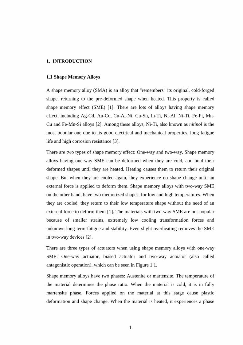
There are three types of actuators when using shape memory alloys with one-way
SME: One-way actuator, biased actuator and two-way actuator (also called
antagonistic operation), which can be seen in Figure 1.1.
Shape memory alloys have two phases: Austenite or martensite. The temperature of
the material determines the phase ratio. When the material is cold, it is in fully
martensite phase. Forces applied on the material at this stage cause plastic
deformation and shape change. When the material is heated, it experiences a phase
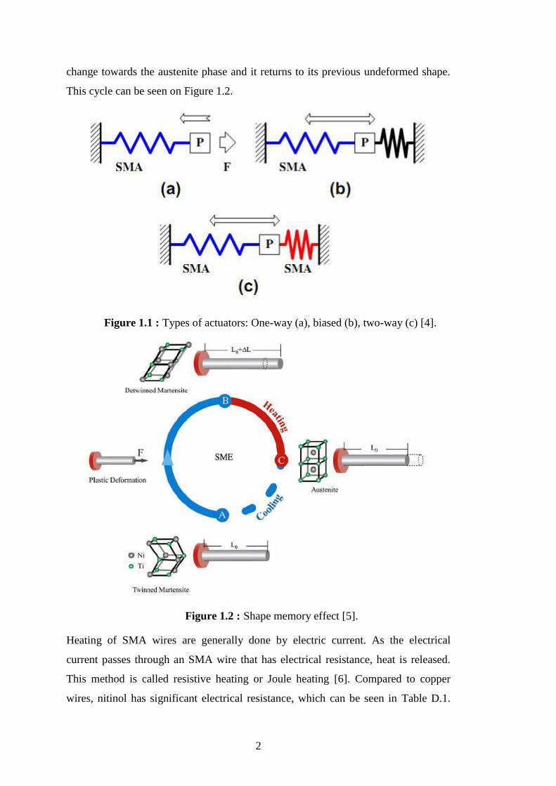
2
change towards the austenite phase and it returns to its previous undeformed shape.
This cycle can be seen on Figure 1.2.
Figure 1.1 : Types of actuators: One-way (a), biased (b), two-way (c) [4].
Figure 1.2 : Shape memory effect [5].
Heating of SMA wires are generally done by electric current. As the electrical
current passes through an SMA wire that has electrical resistance, heat is released.
This method is called resistive heating or Joule heating [6]. Compared to copper
wires, nitinol has significant electrical resistance, which can be seen in Table D.1.

3
Resistive heating is easy to apply but it depends on the resistance of the wires.
Because of that, higher currents are needed to heat thick or short SMA wires, as they
have less electrical resistance. One disadvantage of this method is that there is no
way to cool the SMA wire. When no current is applied to the SMA wire, cooling is
achieved by heat loss caused by lower ambient temperature. In some studies,
thermoelectrical devices are used for active cooling [7]. This method improves the
cooling speed but also increases the complexity of the system, as thermoelectrical
devices require additional space and create additional weight to the actuator entity
[2]. Another method is using SMA wires in water or other fluids to improve cooling
speed, used in [8].
SMA actuators receive increasing interest, due to their high power to mass ratio. This
property makes them a possible alternative to the conventional actuators such as
electric motors. Utilization of SMA actuators greatly reduces the mass of the actuator
itself, which in return reduces the mass of the overall design. The electronic
hardware required to drive them is much simpler than the one needed to drive
conventional electric motors, as the current needs to flow one-way only. Their
mechanical integration to the overall system is also easier, as they do not need any
external components such as gearboxes, which are required by electric motors. Silent
operation can also be considered as an advantage.
Despite their obvious advantages, SMA materials suffer hysteretic behavior, which
makes their control a hard challenge. In addition, their cooling cycle is relatively
long, limiting their operation frequency significantly. Active cooling can be a
solution for long cooling cycles, but this approach cancels the high power to mass
advantage by introducing additional mass and volume to the system. SMA materials
have low power efficiency, because of their low electrical resistance. Although
resistance of SMA wires are high enough to allow resistive heating, the current
required for heating increases with the increasing wire diameter, as thicker wires
have less electrical resistance [2]. In addition, current must be supplied to hold them
in contracted state, which is not the case with electric motors that can hold their state
with no power applied, with the help of mechanical locking systems. Systems
actuated with SMA are also weak against disturbances causing temperature change,
such as external airflows. The behavior of SMA materials directly related with their
temperature, but measuring their temperature is not easy because of physical
4
limitations. The absence of the temperature data makes them even harder to control.
SMA materials also suffer fatigue effects; their maximum strain is reduced after
repeating cycles [9].
As mentioned before, hysteretic behavior of SMA materials makes them hard to
control. To overcome this difficulty, various control methods are tested. Some
researches are focused on determining the hysteretic behavior by utilizing general
hysteresis models, including Preisach and Parandtl - Ishlinskii models [10], [11],
[12]. In some studies, artificial neural networks are trained for obtaining models for
SMA actuators [13], [14]. Reinforcement learning method is used to compensate the
hysteretic behavior with the help of temperature and position data in [15]. PID
control methods with some modifications are also used to avoid obtaining the model
of the SMA materials in [16], [17].
Shape memory alloys find usage in many areas including non-explosive release
mechanisms, proportional pneumatic microvalves, coupling mechanisms, medical
devices, micro-robotics and even in art works [2], [18]. Their implementations in
robotic applications are quite interesting. For example, a 16 DOF mobile robot
utilizing 24 SMA wire actuators and weighs only 26 grams is developed in [19].
1.2 Purpose of Thesis
In this study, the first goal is to create an experimental setup that gives the
researchers to ability to implement various control algorithms and test them with the
SMA wires. Effort is focused on creating a software platform that provides object
oriented programming capabilities. Creating a platform that uses a common object
oriented language such as C++, frees the researchers from the need of vendor
dependent solutions that are generally expensive and not portable to different
platforms.
The second goal is to test various control algorithms on the designed platform to
achieve acceptable performance in position and speed control of SMA wire
actuators. Once an acceptable control algorithm is developed, the next step is
embedding the new controller in a compact embedded computer that can be used in
robotic applications to replace conventional actuator systems, such as electrical
motors.

5
1.3 Organization of Thesis
This thesis is organized as follows:
Chapter one (this chapter) gives a general idea about shape memory alloys. Their
properties, types and behaviors are mentioned. Advantages and disadvantages of
using shape memory alloys as actuators are discussed. Studies testing different
control methods in the literature to overcome some of the disadvantages of shape
memory alloys are mentioned. In addition, application examples of shape memory
alloys are given. Finally, the purpose of the thesis is explained.
Chapter two gives detailed explanations about the experimental setup used for the
SMA test. Both the electronic and software designs are explored, including the failed
design attempts. Circuit schematics of the electronic parts and flow diagrams of the
software are given. Also, object oriented structure of the software is explained in
detail.
Chapter three explains the experimental procedure taken for the position control of
the test load connected to an SMA wire. Tuning of the PID controller with Ziegler -
Nichols methods and its results are mentioned. Actions taken to improve the results
are explained and the results are given. Frequency response of two SMA wires
having different diameters are obtained and compared. Finally, effects of introduced
obstacle in the cooling cycle are observed.
Chapter four summarizes the results of the study. It mentions the outcomes of the
study and the problems encountered in the process. Finally, it gives
recommendations for further study.

6
7
2. EXPERIMENTAL SETUP
2.1 Overview of the Experimental Setup
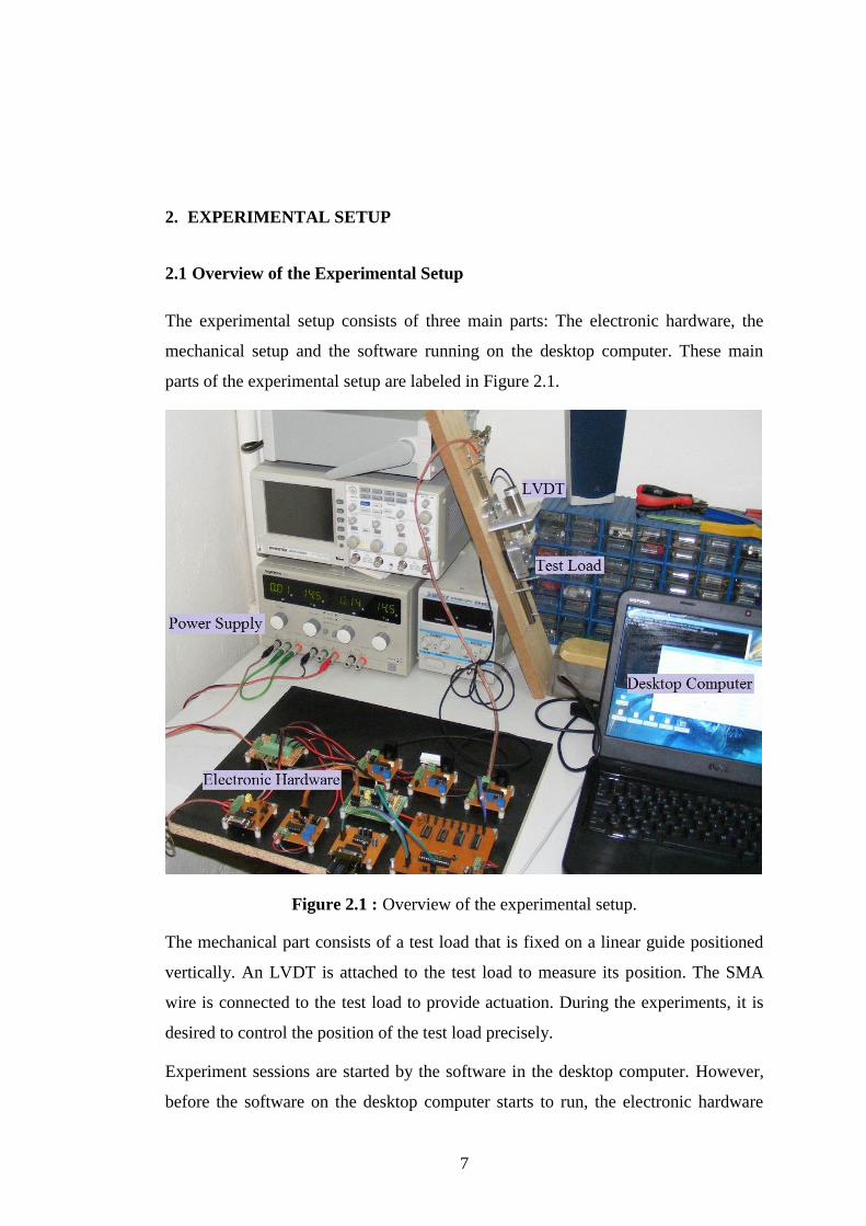
The experimental setup consists of three main parts: The electronic hardware, the
mechanical setup and the software running on the desktop computer. These main
parts of the experimental setup are labeled in Figure 2.1.
Figure 2.1 : Overview of the experimental setup.
The mechanical part consists of a test load that is fixed on a linear guide positioned
vertically. An LVDT is attached to the test load to measure its position. The SMA
wire is connected to the test load to provide actuation. During the experiments, it is
desired to control the position of the test load precisely.
Experiment sessions are started by the software in the desktop computer. However,
before the software on the desktop computer starts to run, the electronic hardware
8
must be powered on. The microcontroller in the electronic hardware executes its
initialization routines in less than a second and waits for the commands from the
software in the computer. The software in the computer is connected to the DAQ
card via serial port. The software provides the current reference for SMA wires. This
reference values are translated into analog signals by the DAQ card to drive SMA
wire drivers. The SMA wire driver maintains the desired current on the SMA wire
with closed loop control. It also measures the voltage drop on the SMA wire. This
information is transferred to the DAQ card to allow it to calculate the resistance of
the SMA wire. As the current supplied by the SMA wire driver heats the SMA wire,
it contracts and moves the test load upwards. When the SMA wire driver decreases
the current value, ambient temperature causes the SMA wire loose heat and expand
with the effect of the test load. The LVDT connected to the test load measures the
position of the test load and generates an analog output that is read by the DAQ card.
The DAQ card sends the information it collects, which are the position of the test
load and the resistance of the SMA wires, to the computer. Then the software in the
computer calculates its next action. This flow can be seen of Figure 2.2.
Figure 2.2 : Relations between the components of the experimental setup.
9
2.2 Design of the Electronic Hardware
2.2.1 Overview of the electronic hardware
Electronic hardware is the bridge between the mechanical part and the software
running on the computer. It consists of SMA wire drivers, the data acquisition card
(main board), voltage limiter board and MAX232 board. The SMA wires and the
LVDT are connected to the electronic part. The whole system is powered by a ±15
volt power supply, but some of the boards have their own voltage regulators. The
electronic system is connected to the desktop computer with serial port, which is
actually a USB to RS232 converter. The parts of the electronic hardware are labeled
on Figure 2.3.
Figure 2.3 : Overview of the electronic hardware.
10
2.2.2 SMA wire driver
2.2.2.1 Design approach
It is necessary to apply current to the SMA wire in order to heat it. Generally, control
circuits are not designed to source high currents, so a driver circuit layer is required
between the main controller and the system itself. In this experimental setup, the
SMA driver must satisfy two requirements:
Controlling the electrical current on the SMA wire
Measuring the electrical resistance of the SMA wire
Controlling the electrical current on the SMA wire is the primary requirement where
the measuring the electrical resistance is the secondary one. However, resistance
measurement process determines which method to use for current control. The
easiest way to measure the current is letting it to pass through a known-value resistor.
The voltage drop on the resistor then can be used to calculate the current. Resistance
of the SMA wire on the other hand, can be calculated by using a similar method:
Measuring the voltage drop on the SMA wire. As the current passing through the
sensing resistor is same as the current on the SMA wire, the resistance of the SMA
wire can be calculated easily. There can be two approaches for current control of the
SMA: Digital and analog control.
Digital control is based on PWM method, where pulses having variable width are
generated by a digital signal generator, which generally is a microcontroller. In this
method, the amplifier switches between zero and maximum current output depending
on the PWM signal generated by the controller. Duty cycle of the PWM signal
determines the mean current value supplied to the SMA wire. In this method, duty
cycle of the PWM signal must be modified according to a current measurement
feedback. Although it is possible to design a voltage controlled PWM generator by
using basic electronic components and integrated circuits, a more convenient way to
do this is using a microcontroller. Most microcontrollers on the market have analog
input capabilities (A/D Converters). PWM generation can be done by using hardware
modules if the microcontroller has one. If the microcontroller lacks the PWM
generator hardware, this feature can still be implemented via software. Using a
microcontroller also allows choosing how to receive the reference signal. The
reference signal can be analog or digital. Analog signal can be retrieved by the

11
microcontroller via the A/D converter. On the other hand, digital signals are
generally data packages obeying a communication protocol. An existing protocol can
be used for the data packages, or a new one can be designed to fit the needs of the
system, although later one is a time consuming task. Unlike retrieving the analog
reference signal, sending the calculated SMA resistance value (or the voltage drop on
the SMA wire) is slightly more complicated as integrated D/A converters in
microcontrollers are not as common as the integrated A/D converters are. Thus,
generating an analog output signal generally requires additional D/A ICs. One
example design using PWM method can be seen in [20].
Analog control on the other hand is based on amplifying a control signal that is
generated by analog electronic components. Analog operations on signals are done
by using operational amplifiers (op-amp). Reference signal is in analog form.
Depending on the circuit design, voltage drop on the sensing resistor and SMA wire
can be measured and amplified directly, or a difference amplifier design may be
needed. Closed loop control design is based on op-amp circuits where the most
common elements are summers, inverters, gains, differentiators and integrators. The
resultant control signal is generally amplified by using transistors or MOSFETs, as
common op-amp ICs are not able to source much current. Of course, some op-amps
are designed to be able to supply high currents, and can be used to drive SMA wires
directly. Audio amplifiers in the market generally satisfy this requirement.
In this experimental setup, an analog SMA driver design is preferred. The main
reason for this choice is the ease of resistance measurement. When PWM signals are
used to drive the SMA wire, the voltage drop on the SMA wire also changes
depending on the PWM signal cycle. This forces accurate timing requirements while
measuring the voltage drop on the SMA wire such that the voltage measurement
must take place while the PWM signal is on high level. Considering that the duty
cycle and thus uptime of the PWM signal is subject to change at any time, achieving
a correct timing of the A/D conversion cycle is a complex task, if not impossible.
The secondary reason of using an analog driver design is that, a circuit having analog
input and output capabilities can interface with a wide range of devices without the
need of a communication protocol. This allows early testing of the SMA driver
circuit with common equipment such as oscilloscope and function generator without
the need of designing other hardware and software that would be required if a digital

12
interface was used. Although receiving an analog signal is easy for a microcontroller,
as mentioned before, generating an analog output signal is slightly more complicated
and costly as it requires additional hardware. Because of this, an analog interface on
a digital SMA driver circuit is not considered. In addition, an analog driver also
eliminates the need of software design in the SMA driver circuit.
The driver is required to be able to supply about 0.5 amperes of current to the SMA
wire. Keeping in mind that most op-amps that can be easily found on the local
market operate in ±15 volt supply interval, one can expect to drive an SMA wire
having a resistance of maximum 30 ohms. In practice, this value is lower when the
losses in the amplifier and sensing resistor are considered. Of course, the driver can
drive SMA wires with higher resistance values, but the maximum current it can
supply will be decreased accordingly.
Intervals of the analog input and output signals are also subject to some limits.
Although modern data acquisition systems are generally capable of accepting analog
inputs in ±10 volts interval, most of microcontroller based circuits can not accept
negative voltage levels. 5 or 3.3 volt supplies are generally used for microcontroller
based designs, and this value also limits both internal and external A/D and D/A
components. Because of this, it is desired that both input and output voltages of the
SMA driver circuit are kept in 0 - 5 volts interval.
Once the input and output levels are determined, next follows the scaling of the
signals. As the 0 - 5 volt input signal is desired to drive 0 - 0.5 amperes current, a
gain of 10 is to be added on the feedback line. Another option could be adding a gain
of 0.1 on the input signal line, but it is avoided, as a weakened signal is more prone
to external noise. As mentioned before, the SMA driver circuit design is based on the
assumption that a ±15 volts symmetrical power supply will be used. This value is
also the maximum voltage drop that can be observed on the SMA wire, which
actually is expected to be lower due to losses. It is clear that this voltage drop of
maximum 15 volts must be scaled down to 0 - 5 volts interval. This requirement can
be easily satisfied by adding a gain of 0.3 on the output line, which in practice is the
gain of the differential amplifier block.
13
2.2.2.2 High KP controller
A literature search on internet for voltage controlled current sources often reveals
single op-amp solutions where the voltage drop of a shunt resistor is used as
feedback by connecting it to the inverting input of the op-amp where the reference
voltage is applied on the non-inverting input. Op-amp output is often used to drive a
transistor or a MOSFET. One example of such a circuit can be seen in Figure 2.4.
Figure 2.4 : Basic current controller circuit [21].
Of course, this design is a simple current sink and the load resistor is not included in
the schematic. Based on this design, the load resistor, which is the SMA wire in this
case, is added to the circuit. To measure the voltage drop on the SMA wire, a
differential amplifier is also required as the lower end of the SMA wire is connected
to the sensing resistor instead of the ground. The schematic of the designed SMA
driver can be seen in Figure 2.5. Schematic is created with a free and open source
EDA software called KiCad. A non-inverting amplifier block can be seen on the
feedback line, which allows adjusting the feedback gain via a trimpot. Current
sensing resistor is chosen to be 1 ohm and 1 W rated, although no more than 0.25 W
of power dissipation is expected on this resistor.
Using KiCad, the PCB of the circuit is designed and produced. Figure B.1 shows a
screenshot of the routed PCB design. The PCB has a size of 5 × 5 cm. Four mounting
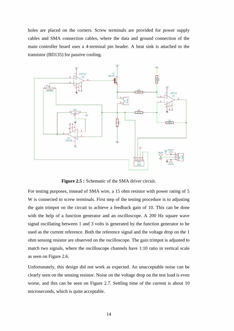
14
holes are placed on the corners. Screw terminals are provided for power supply
cables and SMA connection cables, where the data and ground connection of the
main controller board uses a 4-terminal pin header. A heat sink is attached to the
transistor (BD135) for passive cooling.
Figure 2.5 : Schematic of the SMA driver circuit.
For testing purposes, instead of SMA wire, a 15 ohm resistor with power rating of 5
W is connected to screw terminals. First step of the testing procedure is to adjusting
the gain trimpot on the circuit to achieve a feedback gain of 10. This can be done
with the help of a function generator and an oscilloscope. A 200 Hz square wave
signal oscillating between 1 and 3 volts is generated by the function generator to be
used as the current reference. Both the reference signal and the voltage drop on the 1
ohm sensing resistor are observed on the oscilloscope. The gain trimpot is adjusted to
match two signals, where the oscilloscope channels have 1:10 ratio in vertical scale
as seen on Figure 2.6.
Unfortunately, this design did not work as expected. An unacceptable noise can be
clearly seen on the sensing resistor. Noise on the voltage drop on the test load is even
worse, and this can be seen on Figure 2.7. Settling time of the current is about 10
microseconds, which is quite acceptable.
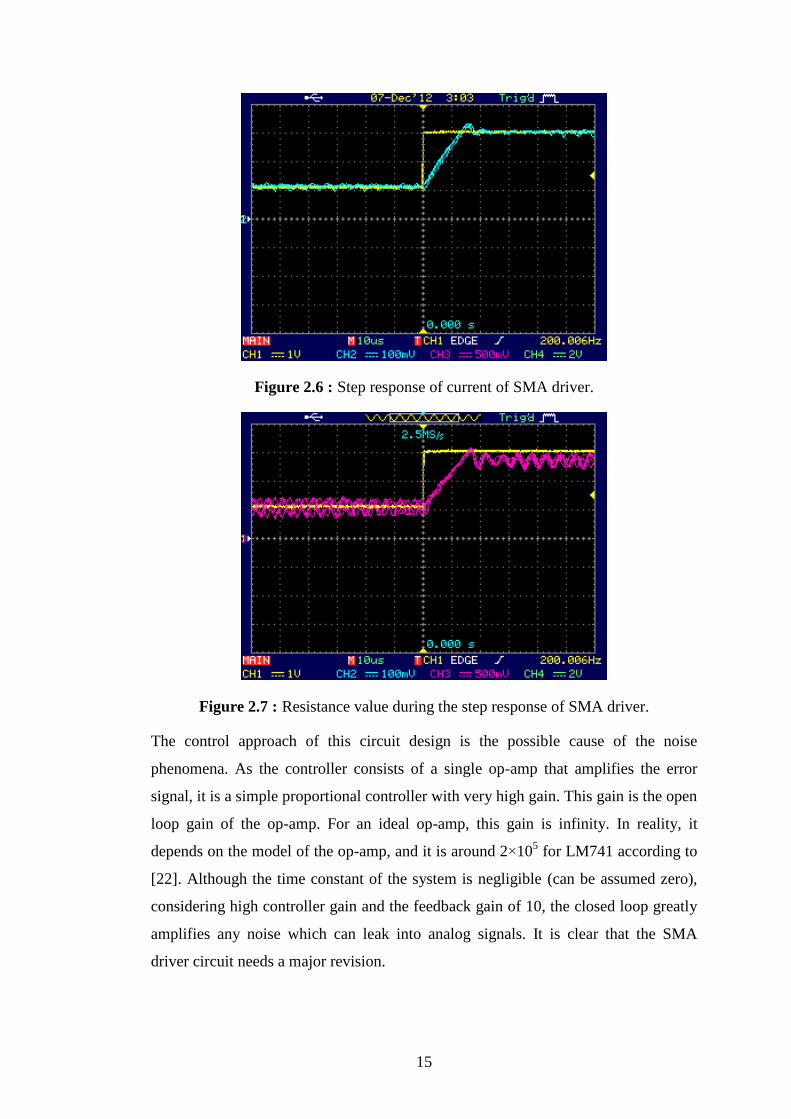
15
Figure 2.6 : Step response of current of SMA driver.
Figure 2.7 : Resistance value during the step response of SMA driver.
The control approach of this circuit design is the possible cause of the noise
phenomena. As the controller consists of a single op-amp that amplifies the error
signal, it is a simple proportional controller with very high gain. This gain is the open
loop gain of the op-amp. For an ideal op-amp, this gain is infinity. In reality, it
depends on the model of the op-amp, and it is around 2×10⁵ for LM741 according to
[22]. Although the time constant of the system is negligible (can be assumed zero),
considering high controller gain and the feedback gain of 10, the closed loop greatly
amplifies any noise which can leak into analog signals. It is clear that the SMA
driver circuit needs a major revision.
16
2.2.2.3 Pure integrator controller
As mentioned before, a simple proportional controller with high gain is not suitable
for the system. Reducing the KP to a lower value would not work either; although
low KP values could overcome the noise problem, an unacceptable steady state error
would remain in the response, as the system has no integrator.
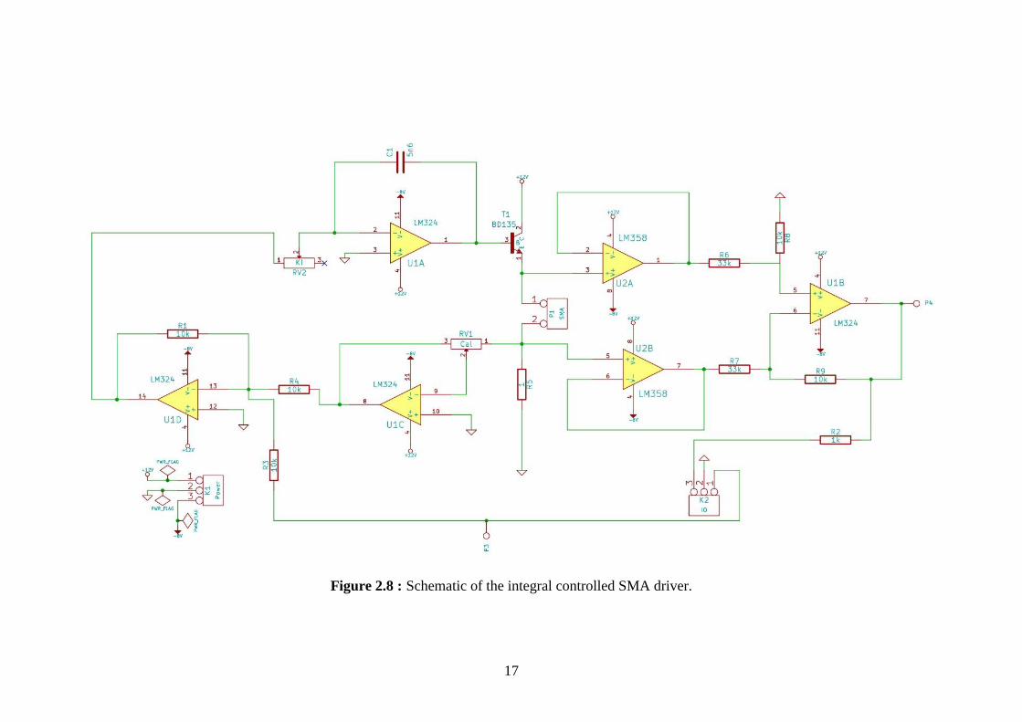
Keeping these facts in mind, a controller based on pure integrator is designed. The
schematic of the new design can be seen on Figure 2.8. Buffer op-amps are added to
input lines of the differential amplifier. Also, a summing amplifier for calculating the
error signal is added just before the integrator. Integrator gain KI is adjustable via a
trimpot, as well as the feedback gain.
The new PCB design looks similar but the analog interface is reduced to 3 lines as it
is concluded that current feedback is not required by the main controller. It now has
two trimpots that are used to adjust the feedback gain and the integrator gain KI. The
routed PCB design can be seen on Figure B.2. The PCB design also benefits of
surface mount resistors to make it possible to fit on a 5 x 5 cm board even with the
presence of additional components. Two testing points are also added to allow easy
access to input and output signals. In a previous version of the PCB design for the
same schematic, surface mount package of LM358 is used at the back side of the
PCB. This approach was abandoned after some circuit failures were observed in form
of arcs between closely routed power traces.
The testing procedure of the new PCB design is similar to the previous one.
Additional to the feedback gain, the integrator gain also needs to be tuned. The first
step is tuning the feedback gain to achieve a gain of 10 on the feedback line. After
that, the integrator gain is increased until any sign of oscillation is observed. This
decreases the settling time of the system.
The test results of the new SMA driver design are quite satisfactory. There is no
noticeable noise on the voltage drops on both sensing resistor and the test load
resistor. System settling time is around 10 microseconds. This can be seen on Figure
2.9. Figure 2.10 shows the measured current drop on the SMA, which is used to
calculate the resistance of the SMA wire. When compared to Figure 2.7, the
improvement is obvious. If the integrator gain KI is increased too much, serious
oscillations are observed as seen on Figure 2.11.
17
Figure 2.8 : Schematic of the integral controlled SMA driver.

18
Figure 2.9 : Step response of current of the new SMA driver.
Figure 2.10 : Resistance value during the step response of SMA driver.
Figure 2.11 : High KI causing oscillations.

19
Low pass filter characteristic of integrators are well known, thus a frequency
response test is required to determine the maximum frequency that the driver circuit
is able to follow. A sine wave oscillating between 1 - 3 volts interval is used for the
test. As it can be seen in Figure 2.12, the driver circuit is able follow 1 kHz input
almost perfectly. Some lag can be observed in Figure 2.13 when the frequency is
increased to 10 kHz, but the response is still quite acceptable. Considering that the
driver circuit will be driven at frequencies no higher than 100 Hz, it can be
concluded that the frequency response of the driver circuit is satisfactory.
Figure 2.12 : Frequency response of SMA driver at 1 kHz.
Figure 2.13 : Frequency response of SMA driver at 10 kHz.
20
2.2.3 Voltage limiter
Although the output signal of the LDVT used in the experimental setup is rated
between 0 - 5 volts interval, tests show that the output signal can exceed these values
when the shaft of the LVDT is placed outside of the rated measuring range. Signals
exceeding the rated interval may cause damage to the A/D converter module of the
main control board, as the interval is same as the working range of the module.
Mechanically constraining the movement of the LDVT shaft is not a practical
solution. Thus, a voltage limiter circuit needs to be designed in order to protect the
A/D module of the main control board.
The limiter circuit design is based on the design shared on Hata! Başvuru kaynağı
bulunamadı.. It has a two-stage design. The first stage operates as the upper limit,
while the second stage operates as the lower limit. At upper limit stage, an op-amp in
comparator configuration compares the input signal with a reference voltage, and if
the input signal exceeds the reference voltage, the op-amp sinks the excess voltage
through the diode. This diode prevents the saturated output of the op-amp to corrupt
the input signal, as the op-amp output is at the saturated state if the input signal is
lower than the reference voltage, which is the desired situation. The lower limit stage
works in the same way, except the direction of the diode is reversed. If the input
signal is lower than the reference voltage, output of the op-amp is increased until the
signal reaches the desired value. The schematic of the limiter circuit can be seen on
Figure 2.14, and the PCB design is shown on Figure B.3.
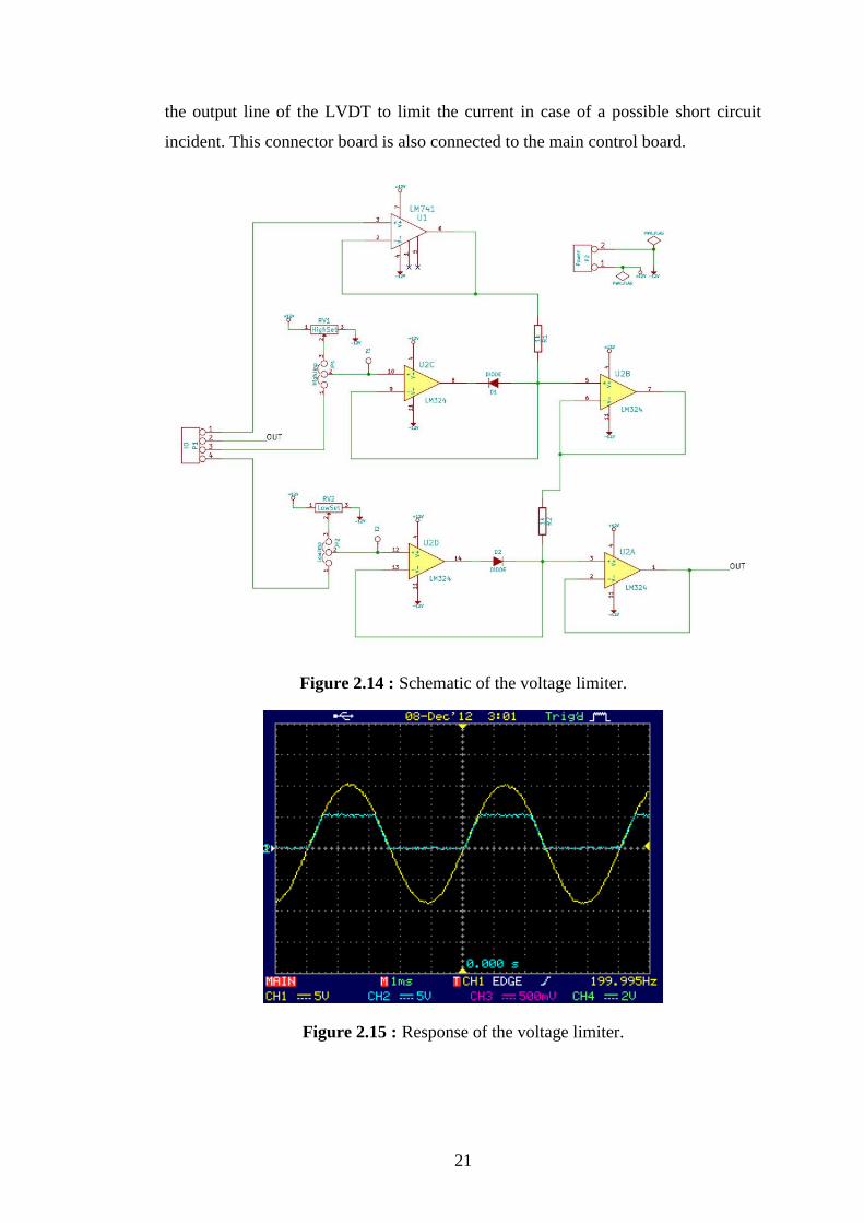
Figure 2.15 shows the testing of the limiter circuit with a 200 Hz sine wave
oscillating between -10 and +10 volts. The trimpots on the circuit are adjusted to
limit the output voltage in 0 - 5 volts interval. The circuit works as expected.
However, if the frequency is increased, circuit fails to response fast enough in case of
voltage inputs that are outside of the reference interval. Although the response can be
improved by using faster diodes, it is not necessary as the operating frequency is
expected to be lower than 10 Hz.
The voltage limiter circuit is not directly connected to the LVDT physically. A
connector board which houses a fuse for protection and a 5 volt voltage regulator
(78L05) to produce upper limit voltage. In addition, a 1 kiloohm resistor is added on
21
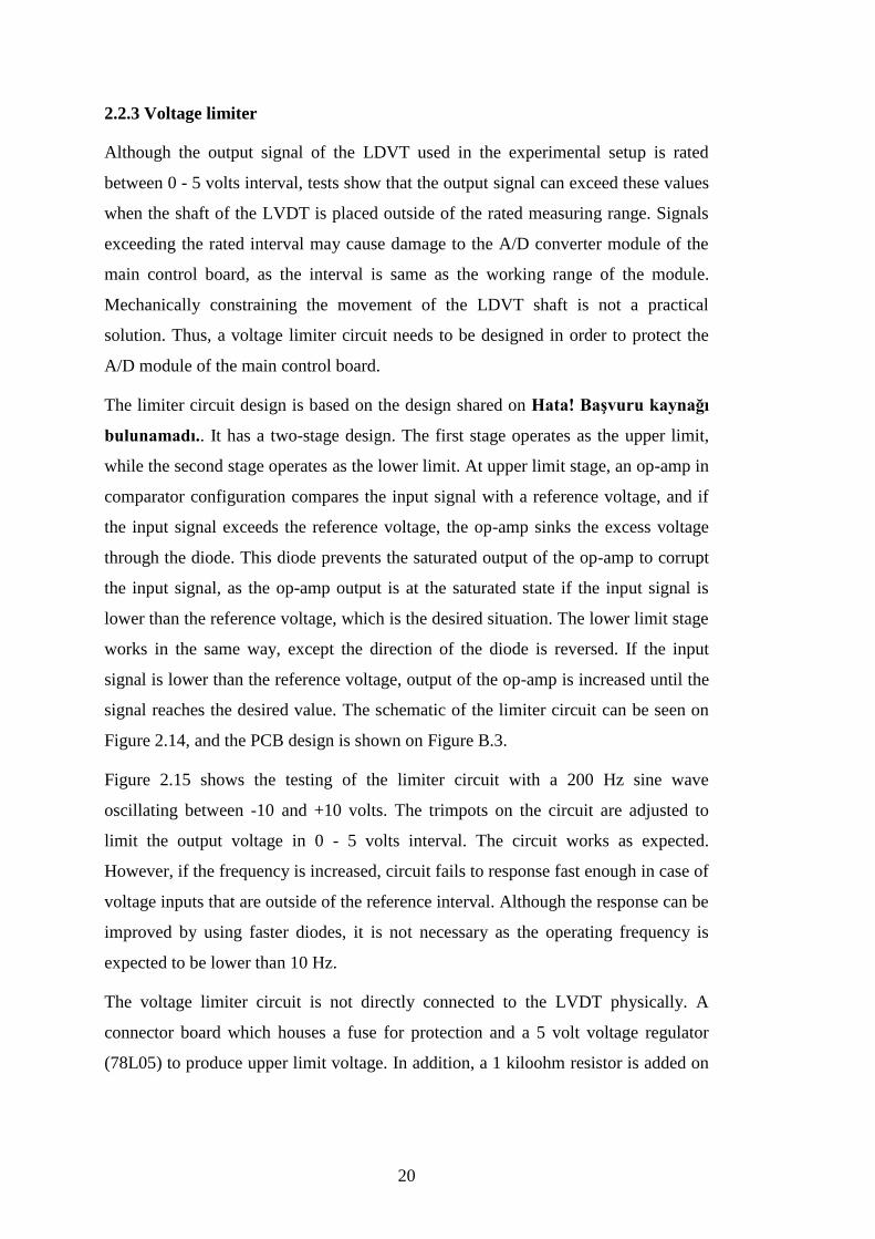
the output line of the LVDT to limit the current in case of a possible short circuit
incident. This connector board is also connected to the main control board.
Figure 2.14 : Schematic of the voltage limiter.
Figure 2.15 : Response of the voltage limiter.
22
2.2.4 Main Board
2.2.4.1 Design approach
The role of the main board in this experimental setup is collecting analog data from
available resources, processing the data by itself or with external processing units,
and then generating the analog control signals for the actuators. The input resources
are the LDVT, SMA wire driver circuits as they measure the voltage drop on the
SMA wire, and a load cell that is planned to be included in the experimental setup in
future. Actuators are the SMA wire driver circuits, which control the current on the
SMA wires according to the control signals received from the main board.
The design of such a board depends on where the control algorithm is planned to be
run on. Generally, off-the-shelf DAQ cards that can be found on the market are
connected to computers via different communication interfaces where the PCI bus
and USB are the most common methods. Vendors of these cards generally provide a
software suite to satisfy the data acquisition and control needs of the customer. In
cases where no large-scale software suite is provided, the vendor provides software
libraries to communicate with the hardware they sell, which enables programmers to
develop their own software using these libraries. An embedded control card on the
other hand, does not require a host computer to operate as it contains the required
software within.
As mentioned earlier, off-the-shelf products often come with complicated software
suites, which provide rapid development capability. However eventually, the design
must be moved to an embedded computer, where the complicated software suites are
generally not supported. In the early stages of the SMA wire driver design, initial
tests are done with PCIe-6259 DAQ card from National Instruments Corporation and
LabView software suite from the same vendor. This setup is later abandoned, to be
able to develop portable and vendor independent software.
In the design of the control board, a hybrid approach is preferred. It is clear that
starting the development cycle on an embedded system is not a good approach,
because of the limited performance and debugging capabilities of these platforms.
Keeping this in mind, the control board is designed to be connected with a desktop
computer. In this design, the control board is simply an A/D and D/A module
extension to the computer. Control algorithms are run on the desktop computer

23
where the data logging, data visualization and user interaction also takes place. The
control card is a microcontroller based design, which can be programmed to operate
without a host computer. This allows that an algorithm can be embedded into the
control card after it is proven to be successful. Of course, algorithms that are beyond
the hardware capabilities of the microcontroller may require some optimizations or
migrating to a high performance microcontroller.
The control card is designed to be able to drive 8 SMA wire drivers. As each SMA
wire driver requires 1 analog input and 1 analog output, it is clear that at least 8 input
and 8 output channels are required. Additional 2 analog input channels are needed
for LVDT and load cell connections. A serial communication interface is also needed
to be able to communicate with a desktop computer.
The control card is based on PIC18F2520 microcontroller from Microchip
Technology Corporation. Some of the important features of this microcontroller are
as follows, taken from [24]:
8-bit Harvard architecture with 16-bit wide instructions
Up to 10 MIPS operating speed
32 kb of program memory, 1536 bytes of SRAM and 256 bytes of EEPROM
25 general purpose I/O channels
10 channel, 10-bit A/D converter
SPI, I2C and USART hardware modules for serial communication
8 x 8 single cycle hardware multiplier
2 PWM channels
PIC18F2520 is easy to obtain from local market and reasonably priced. It is available
in DIP28 package (along with other package options) which is suitable for
prototyping. It is chosen primarily due to author’s prior experience with the PIC18
family microcontrollers, and the availability of software development environment
with no cost. Hardware serial communication module and 10-channel A/D converter
is also effective in the choice. The microcontroller lacks D/A converters, but this
situation is same with the most of 8-bit microcontrollers in the market. D/A
capabilities are planned to be included with additional hardware.

24
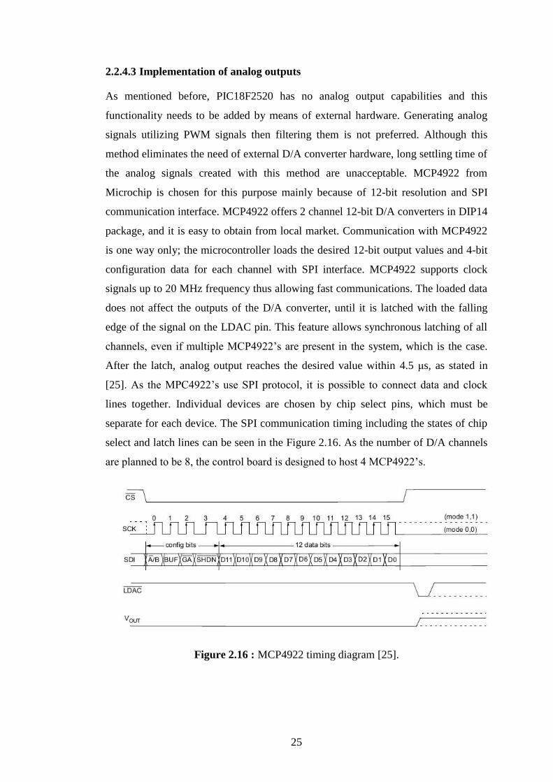
2.2.4.2 Development environment
Microchip provides C compilers for their PIC microcontrollers. Lite editions of these
compilers are free of charge. Compared with the commercial versions, the lite
versions of these compilers lack optimization capabilities, meaning that the code they
produce requires more program memory space and runs slower. Both handicaps are
insignificant, considering that the program memory of the PIC18F2520 is far more
than enough, and the main bottleneck in the execution of the control loop is the serial
communication with the desktop computer, not the speed of the microcontroller
itself. In this design, XC8 compiler is used, which is aimed for 8-bit PIC
microcontrollers. Microchip used to provide some other compilers such as C18 and
Hi-Tech C compilers, but these are now obsolete and not considered as an option.
As the software of the PIC is developed and compiled on a desktop computer, it
needs to be uploaded to the device itself. This process is sometimes called
programming or burning, and requires an additional hardware called programmer or
emulator. Many options are available in the market, but a genuine PicKit 3 from
Microchip is preferred. This device is capable of not only programming PIC family
microcontrollers, but also debugging them. Debugging allows software developer to
connect the device while it is running, and place breakpoints to stop execution of the
program to examine the data inside the device. PicKit 3 is connected to the desktop
computer with USB. Connection to the PIC microcontroller is done by a 5-wire
connection, where these lines are called VPP, VDD, VSS, PGD, PGC. PGD and PGC
are programing interface data and clock pins where VDD and VSS are positive and
negative power supply pins respectively. VPP is carries the programming voltage
which forces the PIC to switch to the programming mode.
Microchip also provides an integrated development environment (IDE), called
MPLAB X, which is based on Netbeans IDE. MPLAB X is capable of being
integrated with various compilers from different vendors. It is also compatible with
the programmers and emulators (including the clones) from Microchip. Usage of
MPLAB X is also required for easy access to debugging capabilities of PicKit 3. A
screenshot of MPLAB X running on Xubuntu Linux can be seen on Figure C.1. It
should be noted that, both XC8 compiler and MPLAB X are operating system
independent, meaning that they can be run on Linux, Windows or MacOS. During
the development of the control board, Linux is used in the desktop computer.
25
2.2.4.3 Implementation of analog outputs
As mentioned before, PIC18F2520 has no analog output capabilities and this
functionality needs to be added by means of external hardware. Generating analog
signals utilizing PWM signals then filtering them is not preferred. Although this
method eliminates the need of external D/A converter hardware, long settling time of
the analog signals created with this method are unacceptable. MCP4922 from
Microchip is chosen for this purpose mainly because of 12-bit resolution and SPI
communication interface. MCP4922 offers 2 channel 12-bit D/A converters in DIP14
package, and it is easy to obtain from local market. Communication with MCP4922
is one way only; the microcontroller loads the desired 12-bit output values and 4-bit
configuration data for each channel with SPI interface. MCP4922 supports clock
signals up to 20 MHz frequency thus allowing fast communications. The loaded data
does not affect the outputs of the D/A converter, until it is latched with the falling
edge of the signal on the LDAC pin. This feature allows synchronous latching of all
channels, even if multiple MCP4922’s are present in the system, which is the case.
After the latch, analog output reaches the desired value within 4.5 μs, as stated in
[25]. As the MPC4922’s use SPI protocol, it is possible to connect data and clock
lines together. Individual devices are chosen by chip select pins, which must be
separate for each device. The SPI communication timing including the states of chip
select and latch lines can be seen in the Figure 2.16. As the number of D/A channels
are planned to be 8, the control board is designed to host 4 MCP4922’s.
Figure 2.16 : MCP4922 timing diagram [25].

26
2.2.4.4 MAX232 sub-board
Direct serial communication is not possible between the PIC18F2520 and the
desktop computer because of different logic levels. PIC18F2520 uses TTL logic
levels, where a voltage levels between 0 - 0.8 volts are considered logic 0 and a
voltage levels between 2 - 5 volts are considered logic 1. Desktop computer on the
other hand, uses RS232 logic levels, where voltage levels from -3 to -25 volts are
considered logic 1 and logic levels from +3 to +25 volts are considered logic 0. For
this reason, a translator circuit is needed between the PIC18F2520 and the desktop
computer. Fortunately, off-the-shelf products are available for this purpose, and a
well-known example of them is MAX232 from Maxim Integrated. This cheap IC is
also easy to obtain from local market, but requires 5 external capacitors of 1 µF
capacity for its voltage doubler and voltage inverter layers. Rather than including this
module in the control board, a separate board is designed for modularity. Circuit
schematic and the PCB design of this circuit can be seen in Figure 2.17 and Figure
B.4, respectively. In addition, as the desktop computer lacks a serial port (new
mainboards often do not have serial ports, as they were generally used for external
dial-up modem connections in the past), a commercial USB to RS232 converter is
used.
Figure 2.17 : Schematic of the MAX232 board.
2.2.4.5 Software in PIC18F2520
The software running in PIC18F2520 is responsible of acquisition of analog data,
time measurement, updating analog outputs and exchanging data with the desktop
computer. The program consists of mainly 4 parts.
27
Initialization Routines
Main Interrupt Service Routine
Low Level Serial Communication Routines
Endless Main Loop
Initialization routines
At the beginning of the program, initializations are required for proper operations of
I/O ports, A/D converter module, serial port module, timer module and interrupts.
I/O port initializations determine the direction of the port pins, as well as their initial
states. 8 pins of the PIC18F2520 are configured to be digital outputs, where one of
them is used to drive the debug LED and the rest are used to drive chip select, data,
clock and latch pins of the MCP4922 array. As MCP4922 reacts to falling edge of
input signals, initial state of their connections must be logic 1. Pins used as analog
channels also need to be configured to be inputs by writing appropriate values to
their direction control registers.
Serial port module is initialized for asynchronous operation with the speed of 115200
bps. Configuration of speed is done by adjusting the overflow limit of a dedicated
timer, which is called SPBRG. This limit depends on the operating frequency of the
PIC18F2520. Both serial transmit and receive functionalities are enabled, as well as
the corresponding interrupts.
A/D converter module is initialized by selecting which pins are used for analog input
purposes. This step is required because any pin that can be configured for analog
input can also operate as a general purpose digital I/O pin. A/D conversion clock is
derived from the main clock of the PIC18F2520, and the division rate must be set for
proper operation. A/D conversion clock frequency determines the speed of the A/D
conversion cycle. The clock frequency must be as high as possible, but must remain
in limits that are specified in the datasheet. Considering this limit (min. 0.7 µs period
[24]), the division rate is adjusted as 32. This gives 1.25 MHz A/D conversion clock
when PIC operates at 40 MHz. Also, automatic acquisition time needs to be adjusted.
Acquisition time is the time needed to charge the input capacitor of the A/D module
to the level of the input signal. A/D conversion cycle can start only after the input
capacitor is charged. Premature start of the conversion cycle may cause error in the
acquired data. Automatic acquisition time is configured as 3.2 µs.

28
Timer0 module is initialized to overflow with constant periods to update the system
tick variable. Timer0 can be run in 8-bit or 16-bit mode. 8-bit mode is selected, as
long overflow periods are not needed. Timer0 clock source can be internal or
external. As it is planned to use for time keeping purposes, internal clock with a
prescaler of 64 is selected. This sets the overflow period to approximately 1.64 ms.
Also, corresponding timer interrupt is enabled.
Last step of the initialization routine is interrupt settings. Individual interrupts
concerning the modules are enabled during their initialization. This step gives the
global permission to interrupts by setting the global interrupt enable bit GIE to 1. In
addition, PIC18 family microcontrollers support 2 level interrupt priority
mechanism; high priority and low priority interrupts. Any interrupt source can be
assigned to a desired priority level. In this program, timer interrupt is assigned as a
high priority interrupt, as it takes almost no time to process it. Serial interface
interrupts are assigned as low priority interrupts.
At the end of the initialization procedures, the debug LED is blinked once to indicate
that initialization step is finished successfully.
Main interrupt service routine
For the sake of simplicity and modularity, the main interrupt service routine is kept
short. There are actually two interrupt vectors, one for each interrupt priority. As
mentioned before, the only high priority interrupt is the timer interrupt. The low
priority interrupt routine on the other hand, handles the serial communications
module transmit and receive interrupts. Figure 2.18 shows a simplified flowchart of
the main interrupt service routine. For simplicity, low and high priority interrupt
routines are not shown separately.
High priority interrupt service routine checks both the interrupt flag and interrupt
enable bits of the timer0 to be sure not responding another interrupt. Then it simply
increments the tick variable by 1, resets the interrupt flag to 0 and exits the routine.
Low priority interrupt service routine first determines the source of the interrupt by
checking both interrupt flag and interrupt enable bits of both receive and transmit
interrupts. According to the situation, it then calls the corresponding interrupt service
routine. These routines are explained in the next section. Serial communications

29
module interrupt service routines are not responsible to clear corresponding interrupt
flags, as they can be cleared only by the hardware.
Figure 2.18 : Flowchart of main interrupt service routine.
Low level serial communication routines
Serial communications is the bottleneck of the execution of the program. Because of
this, it is a good idea to handle serial communications in an interrupt based manner.
Using this method, the microcontroller can continue to operation while serial
communications take place.
Low level communication routines consist of two main parts: Transmit and receive
routines. Both have circular buffers. Low level access functions are interfaces

30
between these buffers and the callers of these functions, or in other words, consumers
and producers.
The serial receive interrupt is always enabled. After receiving a new byte via the
hardware serial port module, a receive interrupt is fired to indicate a new byte is
ready to be read from the hardware register, RCREG. The interrupt service routine
reads the new byte from RCREG and places it on the low level receive buffer. This
routine also keeps record of the bytes that are waiting on the buffer. Consumers
access this buffer via another function, which moves desired number of bytes from
low level buffer to another place in the memory. Function returns the number of
bytes transferred, as the number of desired bytes may be higher than the number of
available bytes. This access routine also updates the variable which indicates the
number of bytes waiting to be read in the low level receive buffer.
The serial transmit interrupt is fired when the hardware transmit shift register is
empty, which indicates that it is not transmitting anything. Because of this, the serial
transmit interrupt is disabled by default as there is no byte to transmit in the
beginning. When enabled, transmit interrupt causes transmit interrupt routine to be
called. This routine moves a byte from low level transmit buffer to hardware register
TXREG. The hardware moves this byte into the transmit shift register, preventing the
transmit interrupt from firing again until transmit of the byte is complete. Transmit
interrupt service routine updates a variable which indicates the number of bytes
waiting in the low level transmit buffer, decreasing it by 1 when a byte is sent. When
this counter reaches to 0, meaning that there are no more bytes waiting to be
transmitted, the interrupt service routine disables the serial transmit interrupt thus
preventing it to be fired again until new bytes are loaded into the low level transmit
buffer. Producers can queue bytes into the low level transmit buffer via another
function, which moves desired number of bytes from another place in the memory
into the low level transmit buffer. This function updates the variable which indicates
the number of bytes waiting in the low level transmit buffer; the variable is increased
by 1. It is also responsible of enabling the serial transmit interrupt.
High level serial communication protocol routines
These routines are the producers and consumers of the low level buffer access
functions. There are two functions, one for receiving data while the other is for
transmitting.

31
The information collected by the control board is stored in a data structure. This data
structure also includes the timestamp of the collected data. When requested by the
desktop computer, the whole data structure is sent. A communication protocol needs
to be immune to possible errors in the physical transport layer, which may cause
corruption of data. In addition, it needs to be generic, which allows it to be
extendable in the future. Although there is currently only one data package format to
transmit, there may be others in the future. A generic protocol must work with all
types of data packages equivalently well. Considering this, a layer between the data
packages and the raw transmit buffer is needed.
The protocol is implemented in a function, which takes a byte pointer showing the
data package to be transmitted, and a size variable indicating the number of bytes to
be transmitted. The function simply inserts a 2-byte preamble data and the size
information that indicates the size of the data package at the beginning. This part is
sent directly by using the low level transmit function mentioned before. At the same
time, a checksum value is calculated for the data package by simply adding all bytes
together to generate a 1-byte value. Overflows are ignored. The low level transmit
function is called again to transmit rest of the data package, which contains the actual
data often called payload. One last call is made to the low level transmit function to
send the checksum byte.
The high level receive function is slightly more complicated. The desktop computer
sends data in a similar way that the microcontroller does, which is explained before.
However, the desktop computer can send any of 3 possible commands whose sizes
are different. Also, the receiving side must keep track of the current state according
to the bytes received before. This logic is often called as “state machines”. A global
or static variable needs to be used to preserve the state information; otherwise, the
state information is lost when the function returns. The high level receive function is
called in the main loop on each iteration. As the low level serial receive buffer is
filled by the interrupt service routine in an asynchronous manner, it is possible for
high level receive function to be called in the middle of receiving a command from
the desktop computer. Thus, it is not unusual for high level receive function to return
in an uncompleted state. The next time it is called, it must be able to continue to
process the low level receive buffer where it left processing on the previous call.

32
The high level receive function acts according to its current state. The state is
updated each time a step is done. First stage is the checking of the preamble data. To
be able to continue, this 2-byte preamble data must be correct. Next stage is the
determination of the package size. Without this information, the receive function can
not know the end of the package, as different types of packages may have different
lengths. This stage is also the stage where the calculation of the checksum is started.
The payload reception state follows next. During this stage, the high level receive
buffer is filled with the incoming data until the package size determined in the
previous stage is reached. The checksum is also calculated, and it is checked after the
payload reception stage ends. If the calculated checksum matches with the last
received checksum byte, the high level receive function returns 1 to indicate that
high level receive buffer contains a valid command. The main loop of the program
acts depending of this return value. If a valid command is received, the main loop
looks for the package ID to determine the action it must take.
Figure 2.19 shows the package frame and four types of payloads used in
communications. Numbers represent the size of that section in bytes. Figure 2.20 on
the other hand, shows a simplified flowchart of the high level receive function.
Figure 2.19 : Data package formats.
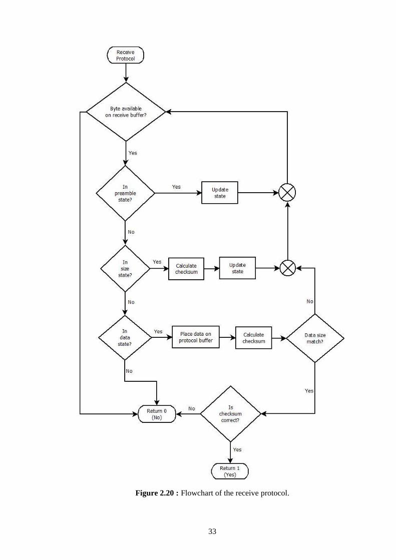
33
Figure 2.20 : Flowchart of the receive protocol.
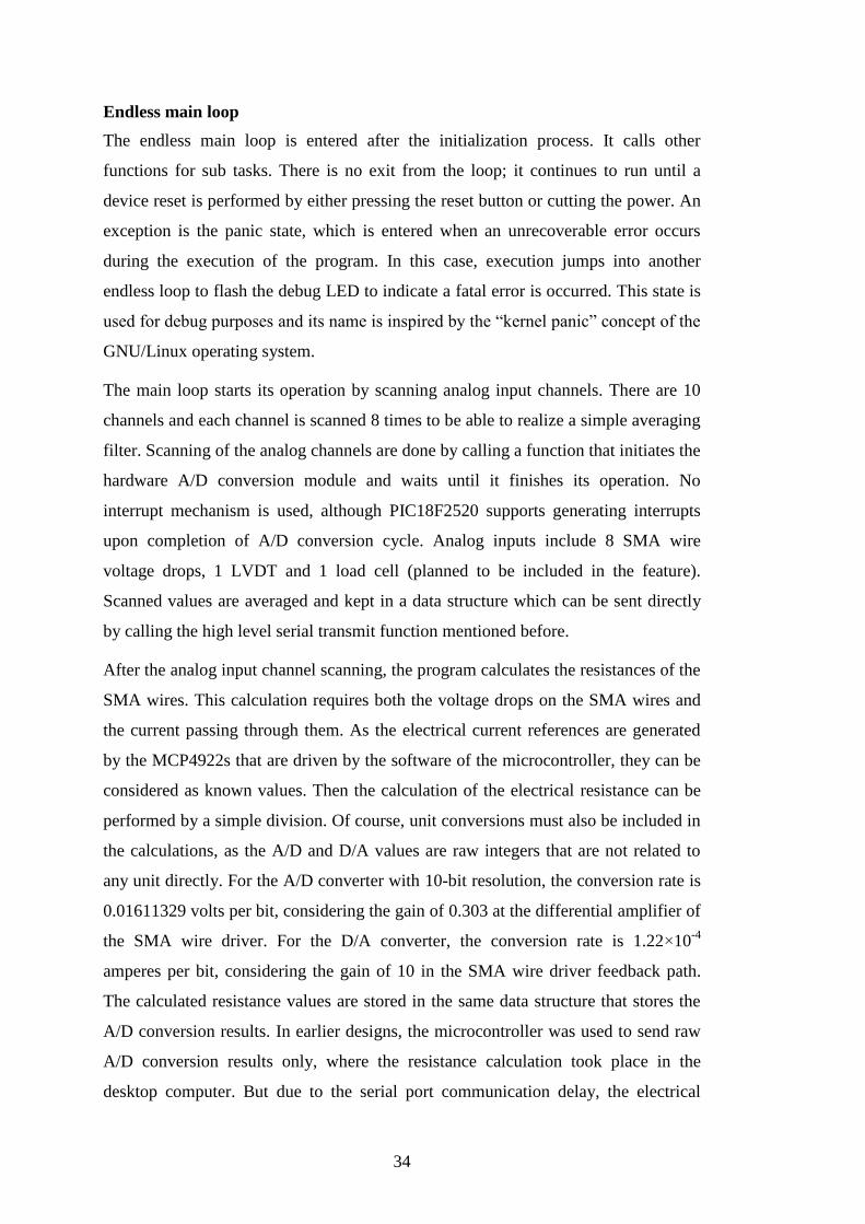
34
Endless main loop
The endless main loop is entered after the initialization process. It calls other
functions for sub tasks. There is no exit from the loop; it continues to run until a
device reset is performed by either pressing the reset button or cutting the power. An
exception is the panic state, which is entered when an unrecoverable error occurs
during the execution of the program. In this case, execution jumps into another
endless loop to flash the debug LED to indicate a fatal error is occurred. This state is
used for debug purposes and its name is inspired by the “kernel panic” concept of the
GNU/Linux operating system.
The main loop starts its operation by scanning analog input channels. There are 10
channels and each channel is scanned 8 times to be able to realize a simple averaging
filter. Scanning of the analog channels are done by calling a function that initiates the
hardware A/D conversion module and waits until it finishes its operation. No
interrupt mechanism is used, although PIC18F2520 supports generating interrupts
upon completion of A/D conversion cycle. Analog inputs include 8 SMA wire
voltage drops, 1 LVDT and 1 load cell (planned to be included in the feature).
Scanned values are averaged and kept in a data structure which can be sent directly
by calling the high level serial transmit function mentioned before.
After the analog input channel scanning, the program calculates the resistances of the
SMA wires. This calculation requires both the voltage drops on the SMA wires and
the current passing through them. As the electrical current references are generated
by the MCP4922s that are driven by the software of the microcontroller, they can be
considered as known values. Then the calculation of the electrical resistance can be
performed by a simple division. Of course, unit conversions must also be included in
the calculations, as the A/D and D/A values are raw integers that are not related to
any unit directly. For the A/D converter with 10-bit resolution, the conversion rate is
0.01611329 volts per bit, considering the gain of 0.303 at the differential amplifier of
the SMA wire driver. For the D/A converter, the conversion rate is 1.22×10⁻⁴
amperes per bit, considering the gain of 10 in the SMA wire driver feedback path.
The calculated resistance values are stored in the same data structure that stores the
A/D conversion results. In earlier designs, the microcontroller was used to send raw
A/D conversion results only, where the resistance calculation took place in the
desktop computer. But due to the serial port communication delay, the electrical

35
current and voltage drop values belonging different time instants were used to
calculate the resistance, causing significant errors as there were approximately 5 to
10 milliseconds between the two sets of data. Because of these errors, this approach
is abandoned and the resistance calculation is moved to PIC18F2520 software.
Although PIC18F2520 has no hardware support for both integer and floating-point
number divisions, the time needed for calculating the resistance is negligible.
After the calculation of the resistance values of SMA wires, the program checks if
there is any commands in the high level serial receive buffer by calling the high level
serial receive function mentioned before. There are 3 possible commands that the
microcontroller can receive: get, dac and latch commands. If there is no command
waiting in the buffer, the high level serial receive function returns 0, but in the
background, it may process the available data and update its state. If there is any
command in the high level receive buffer, the microcontroller responds to that
command before continuing the main loop from the beginning.
The get command is responded by simply pushing the data package collected by the
A/D conversion and resistance calculation processes into the low level serial transmit
buffer by calling the high level serial transmit function. The system tick at the instant
of processing the command is also included in the data package.
The dac command is responded by copying the raw D/A conversion values into
another local storage. This is needed, as the current values sent by the desktop
computer are used in the resistance calculations. Then, the MCP4922 shift routines
are called to push the received values into the MCP4922 array.
Outputs of the MCP4922 array are not updated immediately. This is done after
receiving a latch command, which is responded by microcontroller by flashing the
LDAC output lines connected to the MCP4922 array, causing a synchronous output
update (latch) operation in all MCP4922s. If a command of unknown type is received
due to some error, the execution jumps to panic state.
A simplified flowchart of the execution of the code and the main loop can be seen in
Figure 2.21. The interrupt mechanism is independent from this flow; interrupts are
processed by their own service routines mentioned earlier.

36
Figure 2.21 : Flowchart of the main loop.

37
2.3 Design of the Desktop Computer Software
2.3.1 Design approach
The software running on the desktop computer is the main controller of the system.
The computer software controls the system with the help of the main board that is
responsible of both collection of input data and the generation of the control signals.
As mentioned before, the main control software could be implemented into the
microcontroller of the main board. This approach is not preferred as data
visualization thus debugging of the software is much harder when working with a
microcontroller. Also, the microcontrollers lack the memory and execution speed
advantages of desktop computers. In addition, compilers targeted for low end 8-bit
microcontrollers often do not support object oriented languages such as C++, which
is the case for XC8. Microchip offers C++ compilers only for its PIC32 family
microcontrollers. While using a desktop computer to run the main control algorithm
requires designing a serial communication protocol, it is worth the effort considering
the object oriented language availabilities and debugging capabilities.
There are some requirements to be considered while designing the computer
software. First, the software must have a user interface, which allows the user to start
and stop the control process, change its parameters, and observe the state of the
system. Although a user interface can be text only, considering the capabilities of
modern operating systems, a graphical user interface (GUI) is much more suitable for
the task. It is critical for the system to communicate with the main board with a
minimum delay. This requires a careful design of the serial communication protocol.
In addition, the collected data needs to be logged for later use and it also needs to be
visualized. Online graphing of the live data is the preferred way, but offline plotting
is also acceptable. Finally, although not strictly required, portability of the software
is generally desired.
2.3.2 Development environment
For the software development, Xubuntu is chosen as the host operating system.
Xubuntu is a GNU/Linux distribution that is based on Ubuntu, another popular
GNU/Linux distribution. It is open source and free of charge. GNU/Linux is also
very common in embedded systems, supporting many different processor
architectures, where x86 and ARM architectures are the most popular ones.

38
Multiplatform nature of GNU/Linux increases the portability of the software. The
software developed on a desktop computer running GNU/Linux can later be ported
to an embedded single board computer with minor effort.
C++ is chosen as the programming language used in the software development. C++
is an object oriented language, which provides high portability and performance.
C++ compilers are available for almost any platform, meaning that it is possible to
port a C++ program to another platform with minor effort. Because of this, C++ and
C are the most popular languages for embedded system programming. Java and
Python are also popular, as these high level languages have some advantages over
C++. Although it is easier and faster to develop software in these languages, this
comfort comes with a cost: Reduced performance and higher resource use, which are
generally not acceptable in embedded system design. GCC is chosen as the C++
compiler. GCC actually supports many languages. GCC also supports cross
compiling, which means developing and compiling code for an architecture different
than the host architecture where the compiler runs. The machine that runs the actual
code is referred as the target, and the machine where the code is cross-compiled is
referred as the host. An example is compiling a program on Intel x86 architecture,
where the program is designed to run on an ARM architecture microcontroller. GCC
is open source and free of charge.
C++ language itself does not have an integrated GUI library. The software developer
may choose one according to the needs. For this project, wxWidgets is chosen as the
GUI library. wxWidgets is cross platform library, meaning that it can be used to
design software for GNU/Linux, MacOS of Windows operating systems. wxWidgets
is a C++ based library, but it supports other programming languages as well, with the
help of language bindings. Along with the GUI functionality, wxWidgets also
contains some other functions such as thread management utilities. Qt and GTK+ are
other popular GUI libraries. Unfortunately, later it is discovered that the
documentation and learning resources of wxWidgets are highly scattered across the
web and some major changes between the versions makes it even harder to learn.
The development project continued with wxWidgets, as the time cost of changing the
GUI library could not be afforded in the middle of the development.
The first prototype of the software was actually designed to have a text based user
interface. nCurses was used as the TUI library. nCurses is a very popular TUI library
39
in text based console applications as it does not need X server. Some popular text
based applications using nCurses are vim, emacs, minicom and menuconfig. nCurses
was later abandoned as it was incapable of updating the user interface at the same
time it waits for user input. Attempt to bypass this incapability by implementing a
multithreaded software design caused anomalous behavior, as the nCurses functions
are not thread safe.
Code::Blocks is chosen as the integrated development environment. This choice is
actually due to the failed nCurses based user interface design mentioned before.
Normally, Eclipse would be the IDE of choice as it is very popular and extensible.
Eclipse is a Java based open source software and it is free of charge. Eclipse can also
be well integrated with embedded system design thanks to its extensions, often
referred as plugins. The problem of Eclipse is its built in terminal emulator. Xubuntu
runs in a GUI based manner, which means it runs X server in the background. As the
nCurses is used in text-based applications that run on terminals, a terminal emulator
running in X environment is required. Unfortunately, the built-in terminal emulator
of Eclipse is incapable of running nCurses applications. After the attempts to make
Eclipse use another external terminal emulator was failed, the software development
was migrated to Code::Blocks IDE, which can be configured to call any external
terminal emulator easily. Code::Blocks is nearly as capable as Eclipse, it is
lightweight and it provides smoother user experience as it is not Java based. A
screenshot of the Code::Blocks IDE can be seen on Figure C.2.
GUI design process can be accelerated by using a helper software: wxFormBuilder.
This software makes it possible to design GUI without coding. The user can create
the GUI with simply selecting components with mouse and moving them to their
places in a drag and drop manner. The properties of the GUI components can also be
modified via simple dialog boxes. When requested, wxFormBuilder automatically
generates the code for base classes of the wxWidgets containers. Both the main
source code (.cpp) and the header file (.hpp) are generated for the base class.
wxFormBuilder also helps creating the declarations of the event handlers. This base
class is needed to be expended by a real container class to implement required event
handlers. A screenshot of the wxFormBuilder can be seen on Figure C.3.

40
2.3.3 Thread based structure
In computer science, a thread of execution is the smallest sequence of programmed
instructions that can be managed independently by an operating system scheduler
[26]. In this project, threads are needed to manage operations that must run
concurrently. There are three types of threads in the program:
GUI Thread
Controller Thread
Logger Thread
When the program is started, the GUI thread is in charge. It is responsible of
responding the GUI events such as mouse clicks, keyboard strokes and redrawing of
GUI components. GUI events are bound to event handler functions, such that when a
GUI event occurs, the corresponding event handler is called automatically. Normally,
all functionality of the program may be implemented in event handlers. The problem
is that, the GUI can not do anything while executing an event handler. Therefore, if
an event handler contains a task that takes considerably time to execute, during this
time the GUI is completely frozen and it does not respond to any user action. To
prevent such a behavior, time-consuming tasks need to be executed in separate
threads. Although the term “time consuming” is subjective, generally tasks lasting
more than 1 second are considered time consuming.
The control loop is designed to run until it is stopped by the user. If the control loop
was placed in an event handler, GUI would remain frozen forever and there would be
no way to neither change the control parameters nor stop the control loop. It is clear
that the control loop must be run on a separate thread.
Logger thread on the other hand, is implemented to prevent a bottleneck in the
execution of the control loop. The duty of the logger is to flush the data buffers into
log files in the hard drive when the buffers reach a certain occupancy rate. Hard drive
access generally takes time and may cause a bottleneck in the execution of the
control loop as the thread demanding the hard drive resource is suspended until the
resource is ready. Fortunately, data buffers can be flushed when they are half full.
This allows that the controller thread can fill one half of the buffer, while the logger
thread can flush the other half. Each data buffer is designed to have its own logger
thread.

41
To be able to code multithreaded programs, it is required to use a thread library. On
GNU/Linux systems, threading is based on POSIX threads library, which is often
referred as pthreads, and it is readily available in almost all GNU/Linux distributions.
pthreads is C based and provides functions for creating and managing threads, as
well as data synchronization. But, GUI libraries often provide their own thread
utilities. To prevent possible thread related problems, the wxThread class provided
by wxWidgets library is used in this project. wxThread class is generally used by
extending it by a user defined class.
2.3.4 Object based structure
To achieve a well organized and maintainable software, an object oriented
programming approach is preferred. The program consists of many classes, some of
them having more than one instance. This section summarizes the classes used in the
software. Initialization procedure and the object creation sequence are given in
Appendix A.
A simplified UML diagram showing the class inheritance and aggregation relations
can be seen in Figure 2.22. For the sake of simplicity, class fields and method are not
shown.
Figure 2.22 : Class diagram.

42
Controller: This class is a derived class of wxThread, thus it can be run as a separate
thread. It is also the base class of different type of controller classes. It provides
functions to collect input and release outputs, which are generally called by the child
classes of the Controller. Almost all non-GUI objects are connected to the Controller.
It stores the basic input and output variables of the system such as resistance, tick,
position data received from PIC18F2520, and output data which is to be sent to the
PIC18F2520. Data buffers are also connected to this class. Updating of the data
buffers is also done by this class. This class is generated when a controller type is
selected at the start of the program, and the creation of a Controller object triggers
lots of initialization event.
SerialPort: This class represents a raw serial port access. It is actually ported from a
C code used in the first versions of the software that was written in C. It uses
termios.h header, which provides termios functions describing a general terminal
interface that is provided to control asynchronous communication ports [27]. termios
interface is readily available in almost all GNU/Linux distributions. Later, this C
code is wrapped to form a class, and low level access functions are provided which
read/write desirable number of bytes from/to the serial port. This class initializes the
serial port in raw mode operation, disabling the character based flow control. In
GNU/Linux systems, hardware devices are represented by device nodes, which can
be processed as standard files. Once the settings are done and applied via the termios
interface, this class accesses the serial port via simple file I/O functions.
PicComms: This class is the place where the communication protocol is
implemented. It is responsible to pack raw data into suitable packages. Outgoing
packages are assembled by adding preamble bytes and size information at the
beginning of them. Also, the checksum is calculated and appended to the end of the
package. Data reception is done by first sending a get command to the PIC18F2520
and then waiting for the response. Preamble and size information in the incoming
bytes are filtered out. Checksum is also calculated. If the package passes the
checksum test, it is returned to the calling object, which is a Controller instance.
PicComms class contains a reference to a SerialPort object and calls low level
functions provided by it. The latch command is also implemented in the PicComms
class. It can be callable as a member function and requires no input arguments.

43
SigGen: The signal generator class is responsible of generation the reference signals
for any controller instance. DummyCtrl directly uses these signals as outputs. It can
be configured to generate sine, triangle or square wave signals of different amplitude
and frequency. It also supports varying frequency sine wave generation for frequency
response tests. SigGen functions do not run on a separate thread. Each time a signal
point is required, a time stamp is supplied to the SigGen object to retrieve the signal
for that instant. SigGen is referenced in Controller, SigGenPanel and FreqTestPanel
classes.
SigGenPanel: This class is a GUI component and derived from wxPanel class. It has
a reference to a SigGen object and it is responsible of providing user access to that
SigGen object. SigGenPanel contains various GUI components such as spin controls,
radio buttons and sliders. This components control the signal type, amplitude and
frequency of the SigGen instance it references, via the access functions provided by
the SigGen class. Bearing the properties of wxPanel, the SigGenPanel can be added
into any GUI container. It is referenced by PidCtrlPanel for the reference signal
generation. MainFrame references this class directly when a DummyCtrl instance is
created instead of a PidCtrl instance.
DataPack: DataPack class is resulted from the effort of creating a flexible buffering,
logging and visualization system. Once the software designer wants to observe an
internal variable in the controller, this variable needs to be displayed on screen and at
the same time, the logger thread must be aware of the existence of it to be able to log
it. Prior to its design and implementation, it was not possible to include new
variables to the buffering, logging and visualization system easily without making
major changes in the code. DataPack and its related companion DPBuf makes this
possible. A new variable that is desired to be observed needs to be defined as a class
member. Then, only one line of code is enough to add this variable to a DataPack.
The rest is completed by the initialization mechanism automatically. DataPack does
not actually contain any data; it simply contains only the pointers to the observed
data. Thus, the controller can manipulate the data without being aware of DataPack
itself. DataPack also contains the names of the fields. These names are used in the
GUI representation. Different DataPack instances are referenced by various other
classes. Examples are DPBuf, Logger, Controller and VarDisplay classes. DataPack
class can contain references to double, integer and Boolean type variables.
44
DPBuf: This class makes it possible to generate data buffers from DataPack
templates. Buffer is circular and it can be considered to consist of two halves. Each
DPBuf instance references a Logger instance. When one half of the buffer is full, the
Logger is run to flush that part into the hard drive while the other half can be filled.
DPBuf is not dynamically resizable or reconfigurable. Its structure is determined
during the initialization stage depending on the DataPack argument it is given. Three
DPBuf instances are created during the execution of the program, to store input,
output and internal variables. These buffers are titled as command, measured and
watch. A fourth buffer titled as bodeBuf is created only during the frequency
response test to store the results of the frequency response test. DPBuf instances are
referenced by the Controller, FreqTestCtrl and VarDisplay objects.
Logger: This class is derived class of wxThread. Logger instances are referenced by
DPBuf objects and they are constructed by the initialization process of the DPBuf
objects. Upon initialization, each Logger object creates a log file named as
“timeStamp_bufferName.log” where the timestamp is the number of seconds passes
since 01.01.1970 00:00, and the buffer name is the title assigned to the DPBuf during
its creation. As mentioned before, Logger instances flush the half of the DPBuf they
are connected upon request. The request is made by the owning DBBuf object.
Loggers are initialized by the same DataPack sample which is used to initialize the
related DPBuf. Also, pointers to buffer addresses are supplied to the Logger objects.
VarDisplay: This class is a GUI component and derived from wxPanel class. During
the construction, a DPBuf instance is supplied. The duty of VarDisplay is to display
the last set of variables that are stored in the referenced DPBuf. Bearing the
properties of wxPanel, the VarDisplay can be added into any GUI container.
VarDisplay instances retrieve the last DataPack present in the DPBuf objects to
update the GUI upon a trigger from a wxTimer event. The wxTimer does not run on
a separate thread; instead, it is a part of the main GUI thread. VarDisplay instances
are referenced by the MainFrame class, as they are directly added onto it. As there
are three DPBuf instances in the program, the number of VarDisplay instances is also
three.
MainFrame: This class is the first user defined class that is constructed, and it can be
considered as the entry point of the whole program. Upon its construction, it creates
a wxTimer instance. Then, according to the user input, it creates a controller of
45
appropriate type, which triggers a series of initialization events. Control panels of
controllers and VarDisplay instances are created and contained by the MainFrame.
The event handler of the wxTimer event is also implemented in this class.
PidCtrl: This is the class where the PID control algorithm resides. Derived from the
Controller class, PidCtrl is also a WxThread thus it runs on a separate thread. Upon
starting, this thread enters the control loop that can be ended only by a user
command. On each iteration, the loop collects inputs from the PicComms class that it
references, calculated the control action and releases the output command with the
same PicComms interface. Then it pushes all input, output and watch data on
corresponding buffers. PidCtrl class provides access functions to modify its settings,
such as KP, KI and KD values.
PidCtrlPanel: This class is a GUI component and derived from wxPanel class. It has
a reference to the PidCtrl object. PidCtrlPanel provides user interface controls to
change the behavior of the PidCtrl object is references. It contains the relevant event
handlers.
Averager: Averager is a helper class for calculating the average of streaming values.
Averager contains a self-maintained circular buffer that can be defined in various
sizes, though it is not possible to change the size of the averaging window after the
initialization. Two functions are provided to access Averager instance. One of them
used to introduce new data to the Averager where the other is used to retrieve the
average of the numbers in the buffer. Averager class has references in Controller and
PidCtrl objects.
LineFitter: LineFitter is a helper class for calculating the slope of streaming two-
dimensional data. LineFitter contains a self-maintained circular buffer that can be
defined in various sizes, though it is not possible to change the size of the buffer after
the initialization. Two functions are provided to access LineFitter instance. One of
them used to introduce new data to the LineFitter where the other is used to retrieve
the slope of the data points in the buffer. LineFitter class has a reference in
Controller.
DummyCtrl: This class is a testing controller, which simply collects inputs but
performs no calculations on them. Derived from the Controller class, DummyCtrl is
also a WxThread and it runs on a separate thread. The output is directly derived from

46
the SigGen object DummyCtrl references. DummyCtrl pushes all the input output
and watch data into the corresponding buffers.
FreqTestCtrl: This class is derived from the PidCtrl class to implement testing code
for the frequency response tests. During the frequency response tests, FreqTestCtrl
uses the same control algorithm that PidCtrl uses, by calling a common function
from it. FreqTestCtrl hosts additional algorithms to extract gain, phase and frequency
information from the real time data, by detecting the peak points of both the
reference and the output signals. This data is stored in a separate DPBuf object. A
separate log file allows Bode diagrams to be plotted.
FreqTestPanel: Similar to the SigGenPanel class, FreqTestPanel is a GUI component
and derived from wxPanel class. It has a reference to a SigGen object and it is
responsible of providing user access to that SigGen object. It is designed specifically
for the frequency response tests, and it provides access to the special frequency
response test functions of the SigGen class. This class allows user to specify the
frequency and position intervals of the frequency response test. A button is also
provided to start the test.
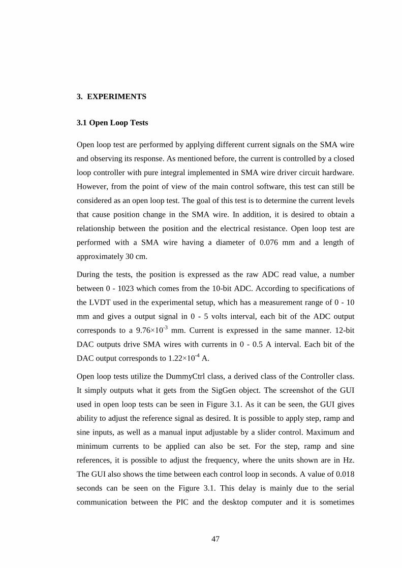
47
3. EXPERIMENTS
3.1 Open Loop Tests
Open loop test are performed by applying different current signals on the SMA wire
and observing its response. As mentioned before, the current is controlled by a closed
loop controller with pure integral implemented in SMA wire driver circuit hardware.
However, from the point of view of the main control software, this test can still be
considered as an open loop test. The goal of this test is to determine the current levels
that cause position change in the SMA wire. In addition, it is desired to obtain a
relationship between the position and the electrical resistance. Open loop test are
performed with a SMA wire having a diameter of 0.076 mm and a length of
approximately 30 cm.
During the tests, the position is expressed as the raw ADC read value, a number
between 0 - 1023 which comes from the 10-bit ADC. According to specifications of
the LVDT used in the experimental setup, which has a measurement range of 0 - 10
mm and gives a output signal in 0 - 5 volts interval, each bit of the ADC output
corresponds to a 9.76×10⁻³
mm. Current is expressed in the same manner. 12-bit
DAC outputs drive SMA wires with currents in 0 - 0.5 A interval. Each bit of the
DAC output corresponds to 1.22×10⁻⁴
A.
Open loop tests utilize the DummyCtrl class, a derived class of the Controller class.
It simply outputs what it gets from the SigGen object. The screenshot of the GUI
used in open loop tests can be seen in Figure 3.1. As it can be seen, the GUI gives
ability to adjust the reference signal as desired. It is possible to apply step, ramp and
sine inputs, as well as a manual input adjustable by a slider control. Maximum and
minimum currents to be applied can also be set. For the step, ramp and sine
references, it is possible to adjust the frequency, where the units shown are in Hz.
The GUI also shows the time between each control loop in seconds. A value of 0.018
seconds can be seen on the Figure 3.1. This delay is mainly due to the serial
communication between the PIC and the desktop computer and it is sometimes
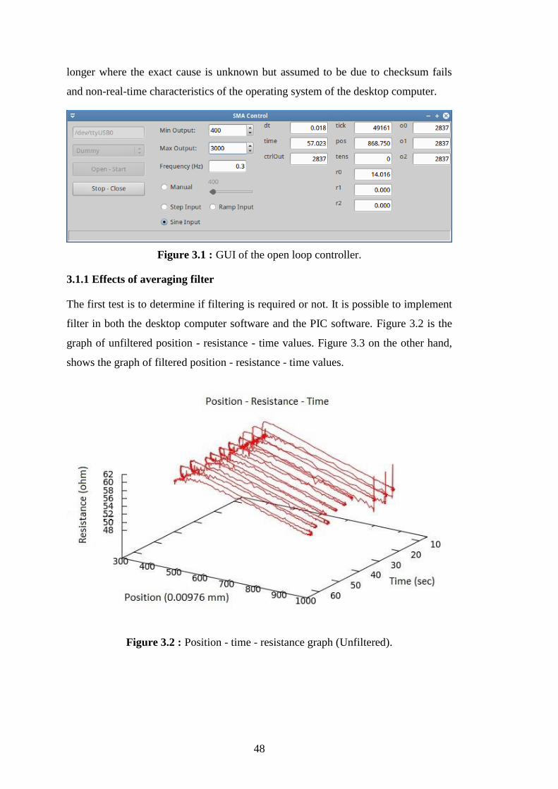
48
longer where the exact cause is unknown but assumed to be due to checksum fails
and non-real-time characteristics of the operating system of the desktop computer.
Figure 3.1 : GUI of the open loop controller.
3.1.1 Effects of averaging filter
The first test is to determine if filtering is required or not. It is possible to implement
filter in both the desktop computer software and the PIC software. Figure 3.2 is the
graph of unfiltered position - resistance - time values. Figure 3.3 on the other hand,
shows the graph of filtered position - resistance - time values.
Figure 3.2 : Position - time - resistance graph (Unfiltered).

49
Figure 3.3 : Position - time - resistance graph (Filtered).
The averaging filters are implemented on both desktop computer and PIC software.
The software in PIC averages the last 8 ADC values, where the software in desktop
computer averages the last 4 values. Experiments show that, the averaging operation
performed in the software of desktop computer is more effective than the averaging
operation performed in the software of PIC. Widening the averaging windows does
not seem to improve the results. Actually, it causes problems in closed loop tests.
3.1.2 Current - position relation
Actually, it is not possible to obtain a direct relationship between the current and the
position, as the position is directly related to the temperature of the SMA wire in a
hysteretic manner. The current indirectly related with the temperature, where a
current that causes heating more than the heat loss of the wire causes it to contract.
Still, this experiment is helpful to determine the rough current levels causing the
SMA wire to contract or extend. Figure 3.4 shows the current - time and position -
time relationship on the same graph. Units are in raw ADC and DAC values as
mentioned before. The Figure 3.5 on the other hand, shows the relationship between
the applied current and the position. Applied current is a sine wave signal. In this
graph, the hysteretic behavior of the SMA wire is clearly visible.
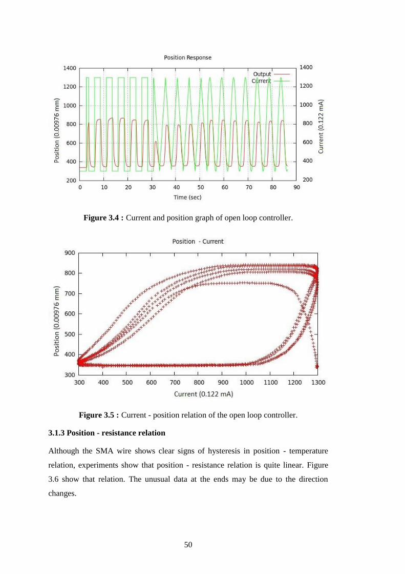
50
Figure 3.4 : Current and position graph of open loop controller.
Figure 3.5 : Current - position relation of the open loop controller.
3.1.3 Position - resistance relation
Although the SMA wire shows clear signs of hysteresis in position - temperature
relation, experiments show that position - resistance relation is quite linear. Figure
3.6 show that relation. The unusual data at the ends may be due to the direction
changes.

51
Figure 3.6 : Position - resistance relation of the open loop controller.
3.2 Closed Loop Tests and PID Controller Tuning
During the closed loop test, a PID controller is implemented and coefficients of the
PID controller are determined. The PidCtrl class, which is a derived class of the
Controller class, hosts the controller algorithm. The GUI is modified to give easy
access to the required controls and data feedback. The interface of SigGen class is
now used to derive the position reference, not the electrical current value directly as
it was in open loop tests. Figure 3.7 shows the modified GUI used for closed loop
tests. As it can be seen, the GUI allows adjusting KP, KD and KI values, as well as the
minimum and maximum current values. Ability to adjust minimum and maximum
current values is a kind of saturation element at the end of the controller output.
Upper limit prevents the SMA wire from overheating thus permanent damage, while
the lower limit prevents the corrupted resistance measurements due to non-ideal
nature of the analog SMA wire driver circuit.
Closed loop tests are performed with SMA wires having diameters 0.076 mm and
0.15 mm. First, the SMA wire with 0.076 mm diameter is used. After a suitable
controller is found, tests are repeated with the SMA wire having 0.15 mm diameter,
by modifying the PID coefficients accordingly.

52
Figure 3.7 : GUI of the closed loop controller.
3.2.1 Tuning by Ziegler - Nichols method
Ziegler - Nichols method is used for the initial tuning of the PID controller. As the
hysteretic behavior of the SMA wire is known, the tuning is based on the actual data
of two different operation intervals, and the obtained coefficients are tested on both
intervals.
The first determination test is performed in between the positions 400 and 800.
During the test, KD and KI are set to zero, and the value of KP is increased by 5 from
0 to the value where it cases undamped oscillations. Figure 3.8 shows this process.
Undamped oscillation state is reached when the KP is 30.
Figure 3.8 : Determination of KCR in 400 - 800 interval.

53
Figure 3.9 shows a close-up of the Figure 3.8, where the two peaks of the oscillating
output are marked to obtain the critical oscillation period PCR. PCR is found to be 0.38
seconds.
Figure 3.9 : Determination of PCR in 400 - 800 interval.
Calculations are made to determine the coefficients for both PI and PID controllers.
A PD controller is not considered as it can be clearly seen that the heating cycle
shows undershoot and steady state error, suggesting that integral action is required.
Table 3.1 shows the calculated coefficients.
Table 3.1 : PID coefficients calculated for 400 - 800 interval.
Kp Ki Kd
PI 13.5 42.6 0
PID 18 94.7 0.8
The performance of PI and PID controllers can be seen on Figure 3.10 and Figure
3.11 respectively. The tests are performed with decaying square reference signals to
test the performance in different operating zones. As it can be seen, both controllers
perform quite acceptable in the zone of 400 - 800 interval where they are tuned. But,
the performance in zone of 550 - 650 interval is not acceptable because of both
overshoot and high oscillations. Derivative term seems to improve the performance
in the zone of 400 – 800 interval, but has no effect in the zone of 550 - 650 interval.

54
Figure 3.10 : Response of PI controller (tuned in 400 - 800 interval).
Figure 3.11 : Response of PID controller (tuned in 400 - 800 interval).
The second determination test is performed in between the positions 550 and 650.
During the test, KD and KI are set to zero, and the value of KP is increased by 5 from
0 to the value where it cases undamped oscillations. Figure 3.12 shows this process.
Undamped oscillation state is reached when the KP is 20.
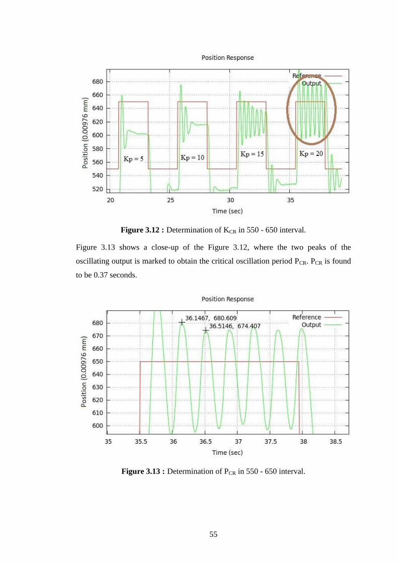
55
Figure 3.12 : Determination of KCR in 550 - 650 interval.
Figure 3.13 shows a close-up of the Figure 3.12, where the two peaks of the
oscillating output is marked to obtain the critical oscillation period PCR. PCR is found
to be 0.37 seconds.
Figure 3.13 : Determination of PCR in 550 - 650 interval.
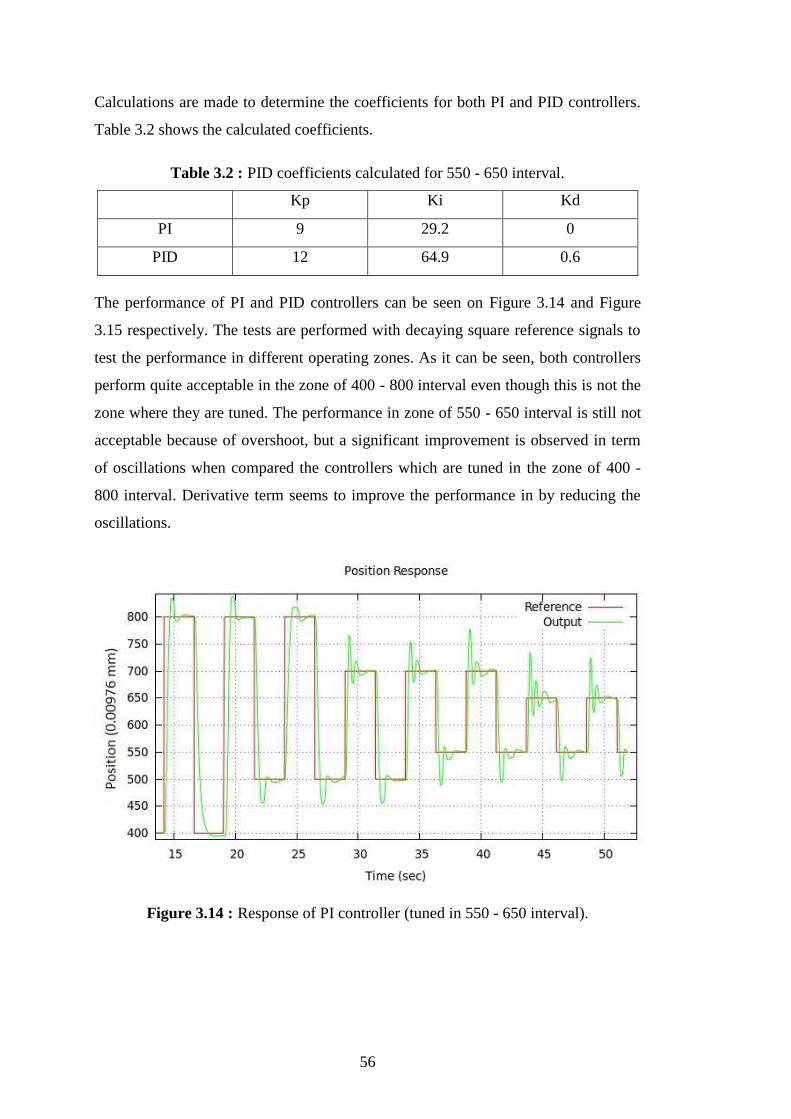
56
Calculations are made to determine the coefficients for both PI and PID controllers.
Table 3.2 shows the calculated coefficients.
Table 3.2 : PID coefficients calculated for 550 - 650 interval.
Kp Ki Kd
PI 9 29.2 0
PID 12 64.9 0.6
The performance of PI and PID controllers can be seen on Figure 3.14 and Figure
3.15 respectively. The tests are performed with decaying square reference signals to
test the performance in different operating zones. As it can be seen, both controllers
perform quite acceptable in the zone of 400 - 800 interval even though this is not the
zone where they are tuned. The performance in zone of 550 - 650 interval is still not
acceptable because of overshoot, but a significant improvement is observed in term
of oscillations when compared the controllers which are tuned in the zone of 400 -
800 interval. Derivative term seems to improve the performance in by reducing the
oscillations.
Figure 3.14 : Response of PI controller (tuned in 550 - 650 interval).
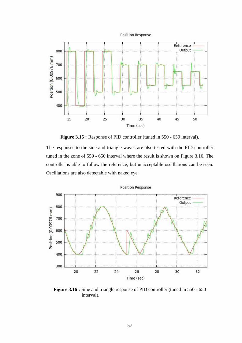
57
Figure 3.15 : Response of PID controller (tuned in 550 - 650 interval).
The responses to the sine and triangle waves are also tested with the PID controller
tuned in the zone of 550 - 650 interval where the result is shown on Figure 3.16. The
controller is able to follow the reference, but unacceptable oscillations can be seen.
Oscillations are also detectable with naked eye.
Figure 3.16 : Sine and triangle response of PID controller (tuned in 550 - 650
interval).
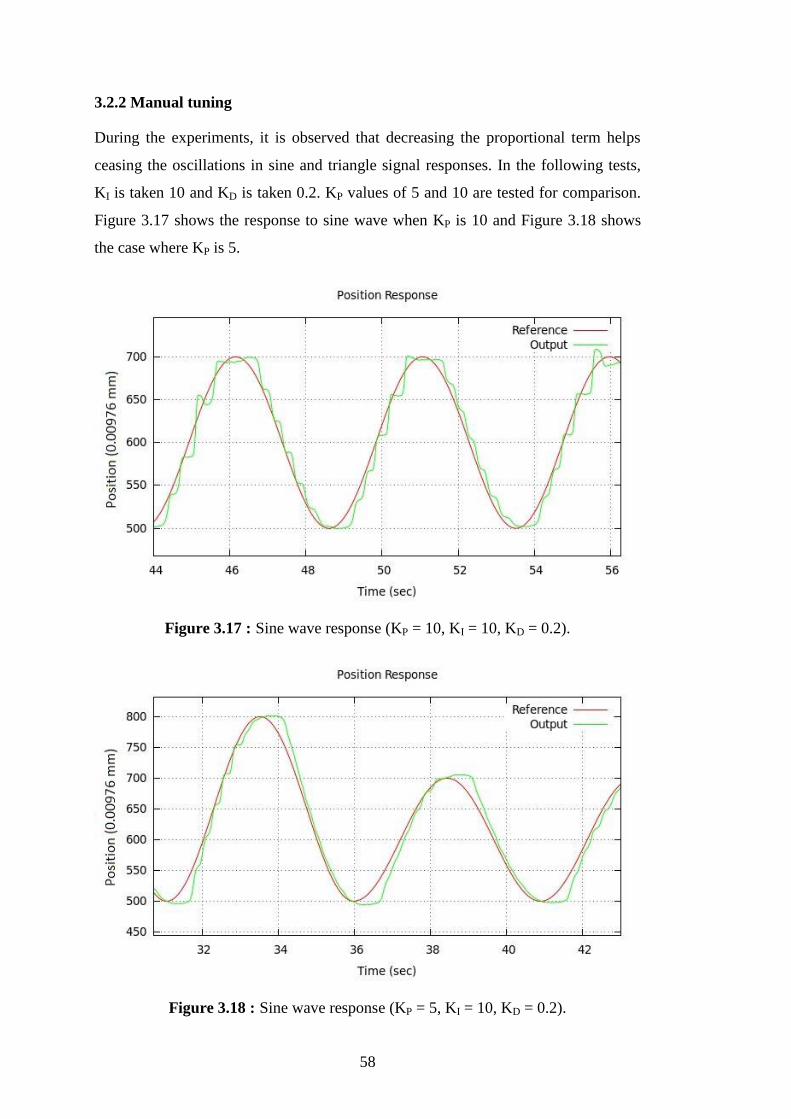
58
3.2.2 Manual tuning
During the experiments, it is observed that decreasing the proportional term helps
ceasing the oscillations in sine and triangle signal responses. In the following tests,
KI is taken 10 and KD is taken 0.2. KP values of 5 and 10 are tested for comparison.
Figure 3.17 shows the response to sine wave when KP is 10 and Figure 3.18 shows
the case where KP is 5.
Figure 3.17 : Sine wave response (KP = 10, KI = 10, KD = 0.2).
Figure 3.18 : Sine wave response (KP = 5, KI = 10, KD = 0.2).

59
It can be clearly seen that decreasing KP from 10 to 5 greatly ceases the oscillations.
The step response of the controller with KP = 5, KI = 10, KD = 0.2 can be seen on the
Figure 3.19, and the step response of the same controller with KI = 20 can be seen on
Figure 3.20.
Figure 3.19 : Step response (KP = 5, KI = 10, KD = 0.2).
Figure 3.20 : Step response (KP = 5, KI = 20, KD = 0.2).
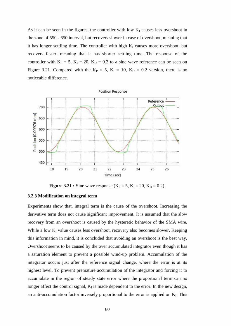
60
As it can be seen in the figures, the controller with low KI causes less overshoot in
the zone of 550 - 650 interval, but recovers slower in case of overshoot, meaning that
it has longer settling time. The controller with high KI causes more overshoot, but
recovers faster, meaning that it has shorter settling time. The response of the
controller with KP = 5, KI = 20, KD = 0.2 to a sine wave reference can be seen on
Figure 3.21. Compared with the KP = 5, KI = 10, KD = 0.2 version, there is no
noticeable difference.
Figure 3.21 : Sine wave response (KP = 5, KI = 20, KD = 0.2).
3.2.3 Modification on integral term
Experiments show that, integral term is the cause of the overshoot. Increasing the
derivative term does not cause significant improvement. It is assumed that the slow
recovery from an overshoot is caused by the hysteretic behavior of the SMA wire.
While a low KI value causes less overshoot, recovery also becomes slower. Keeping
this information in mind, it is concluded that avoiding an overshoot is the best way.
Overshoot seems to be caused by the over accumulated integrator even though it has
a saturation element to prevent a possible wind-up problem. Accumulation of the
integrator occurs just after the reference signal change, where the error is at its
highest level. To prevent premature accumulation of the integrator and forcing it to
accumulate in the region of steady state error where the proportional term can no
longer affect the control signal, KI is made dependent to the error. In the new design,
an anti-accumulation factor inversely proportional to the error is applied on KI. This
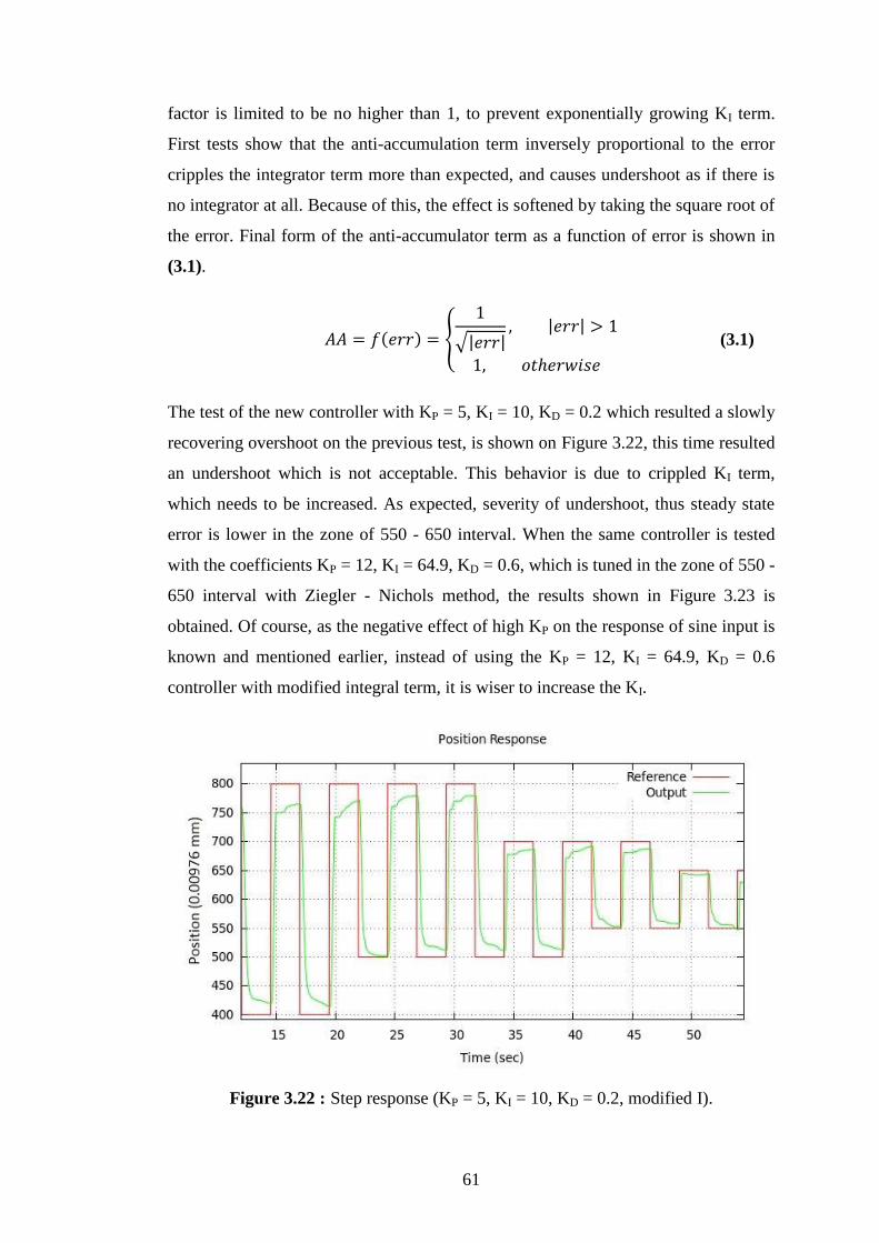
61
factor is limited to be no higher than 1, to prevent exponentially growing KI term.
First tests show that the anti-accumulation term inversely proportional to the error
cripples the integrator term more than expected, and causes undershoot as if there is
no integrator at all. Because of this, the effect is softened by taking the square root of
the error. Final form of the anti-accumulator term as a function of error is shown in
(3.1).
( ) {
√| | | |
(3.1)
The test of the new controller with KP = 5, KI = 10, KD = 0.2 which resulted a slowly
recovering overshoot on the previous test, is shown on Figure 3.22, this time resulted
an undershoot which is not acceptable. This behavior is due to crippled KI term,
which needs to be increased. As expected, severity of undershoot, thus steady state
error is lower in the zone of 550 - 650 interval. When the same controller is tested
with the coefficients KP = 12, KI = 64.9, KD = 0.6, which is tuned in the zone of 550 -
650 interval with Ziegler - Nichols method, the results shown in Figure 3.23 is
obtained. Of course, as the negative effect of high KP on the response of sine input is
known and mentioned earlier, instead of using the KP = 12, KI = 64.9, KD = 0.6
controller with modified integral term, it is wiser to increase the KI.
Figure 3.22 : Step response (KP = 5, KI = 10, KD = 0.2, modified I).
62
Figure 3.23 : Step response (KP = 12, KI = 64.9, KD = 0.6, modified I).
After some test of manual tuning, a controller with KP = 5, KI = 45, KD = 0.2 is found
to be acceptable. Figure 3.24 shows the step response of this controller where Figure
3.25 shows its sine and triangle input response. In the Figure 3.24, the effect of the
crippled integrator can clearly be seen in the zone of 400 - 800 interval, as it
accumulates with an increasing speed after the point where the proportional term can
no longer affect the output. In the zone of 400 - 800 interval, the settling time is
longer but still acceptable.
Figure 3.24 : Step response (KP = 5, KI = 45, KD = 0.2, modified I).

63
Figure 3.25 : Sine and triangle response (KP = 5, KI = 45, KD = 0.2, modified I).
The same control method is also applied for the SMA wire having 0.15 mm
diameter. Coefficients of the PID controller are hand tuned and determined as KP =
20, KI = 70, KD = 0.4. Step response of the thick wire can be seen on Figure 3.26.
Figure 3.26 : Step response of the thick (0.15 mm) wire.
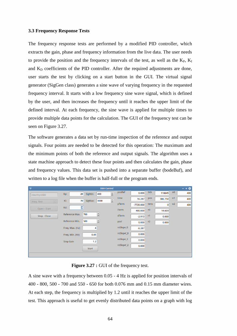
64
3.3 Frequency Response Tests
The frequency response tests are performed by a modified PID controller, which
extracts the gain, phase and frequency information from the live data. The user needs
to provide the position and the frequency intervals of the test, as well as the KP, KI
and KD coefficients of the PID controller. After the required adjustments are done,
user starts the test by clicking on a start button in the GUI. The virtual signal
generator (SigGen class) generates a sine wave of varying frequency in the requested
frequency interval. It starts with a low frequency sine wave signal, which is defined
by the user, and then increases the frequency until it reaches the upper limit of the
defined interval. At each frequency, the sine wave is applied for multiple times to
provide multiple data points for the calculation. The GUI of the frequency test can be
seen on Figure 3.27.
The software generates a data set by run-time inspection of the reference and output
signals. Four points are needed to be detected for this operation: The maximum and
the minimum points of both the reference and output signals. The algorithm uses a
state machine approach to detect these four points and then calculates the gain, phase
and frequency values. This data set is pushed into a separate buffer (bodeBuf), and
written to a log file when the buffer is half-full or the program ends.
Figure 3.27 : GUI of the frequency test.
A sine wave with a frequency between 0.05 - 4 Hz is applied for position intervals of
400 - 800, 500 - 700 and 550 - 650 for both 0.076 mm and 0.15 mm diameter wires.
At each step, the frequency is multiplied by 1.2 until it reaches the upper limit of the
test. This approach is useful to get evenly distributed data points on a graph with log
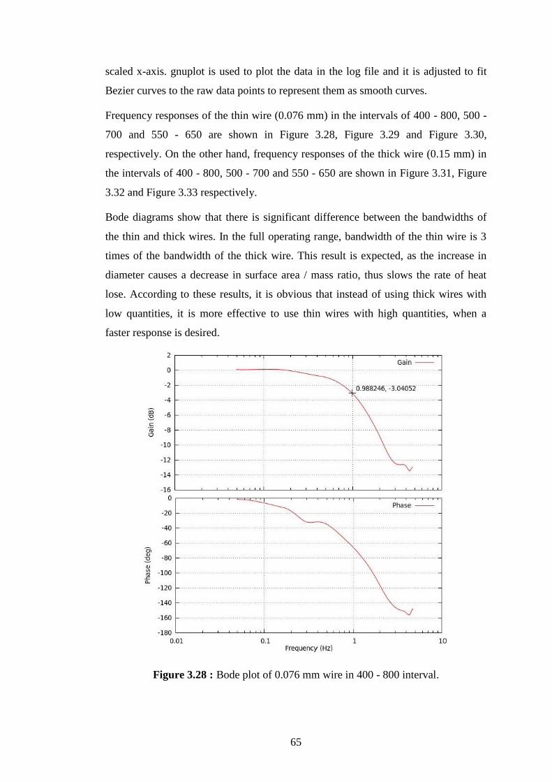
65
scaled x-axis. gnuplot is used to plot the data in the log file and it is adjusted to fit
Bezier curves to the raw data points to represent them as smooth curves.
Frequency responses of the thin wire (0.076 mm) in the intervals of 400 - 800, 500 -
700 and 550 - 650 are shown in Figure 3.28, Figure 3.29 and Figure 3.30,
respectively. On the other hand, frequency responses of the thick wire (0.15 mm) in
the intervals of 400 - 800, 500 - 700 and 550 - 650 are shown in Figure 3.31, Figure
3.32 and Figure 3.33 respectively.
Bode diagrams show that there is significant difference between the bandwidths of
the thin and thick wires. In the full operating range, bandwidth of the thin wire is 3
times of the bandwidth of the thick wire. This result is expected, as the increase in
diameter causes a decrease in surface area / mass ratio, thus slows the rate of heat
lose. According to these results, it is obvious that instead of using thick wires with
low quantities, it is more effective to use thin wires with high quantities, when a
faster response is desired.
Figure 3.28 : Bode plot of 0.076 mm wire in 400 - 800 interval.

66
Figure 3.29 : Bode plot of 0.076 mm wire in 500 - 700 interval.
Figure 3.30 : Bode plot of 0.076 mm wire in 550 - 650 interval.
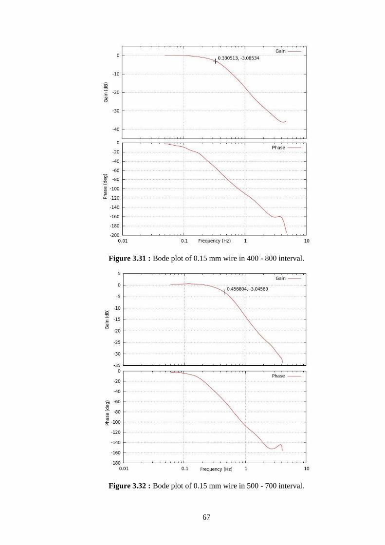
67
Figure 3.31 : Bode plot of 0.15 mm wire in 400 - 800 interval.
Figure 3.32 : Bode plot of 0.15 mm wire in 500 - 700 interval.
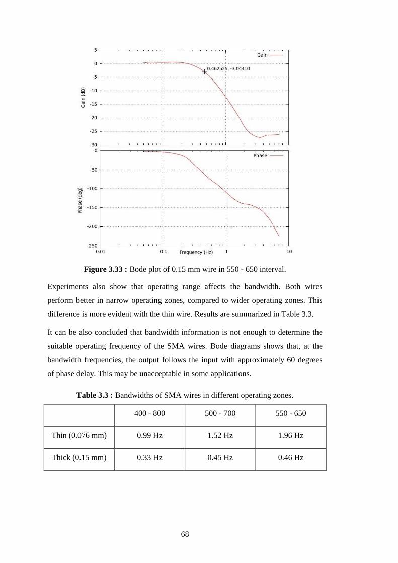
68
Figure 3.33 : Bode plot of 0.15 mm wire in 550 - 650 interval.
Experiments also show that operating range affects the bandwidth. Both wires
perform better in narrow operating zones, compared to wider operating zones. This
difference is more evident with the thin wire. Results are summarized in Table 3.3.
It can be also concluded that bandwidth information is not enough to determine the
suitable operating frequency of the SMA wires. Bode diagrams shows that, at the
bandwidth frequencies, the output follows the input with approximately 60 degrees
of phase delay. This may be unacceptable in some applications.
Table 3.3 : Bandwidths of SMA wires in different operating zones.
400 - 800 500 - 700 550 - 650
Thin (0.076 mm) 0.99 Hz 1.52 Hz 1.96 Hz
Thick (0.15 mm) 0.33 Hz 0.45 Hz 0.46 Hz
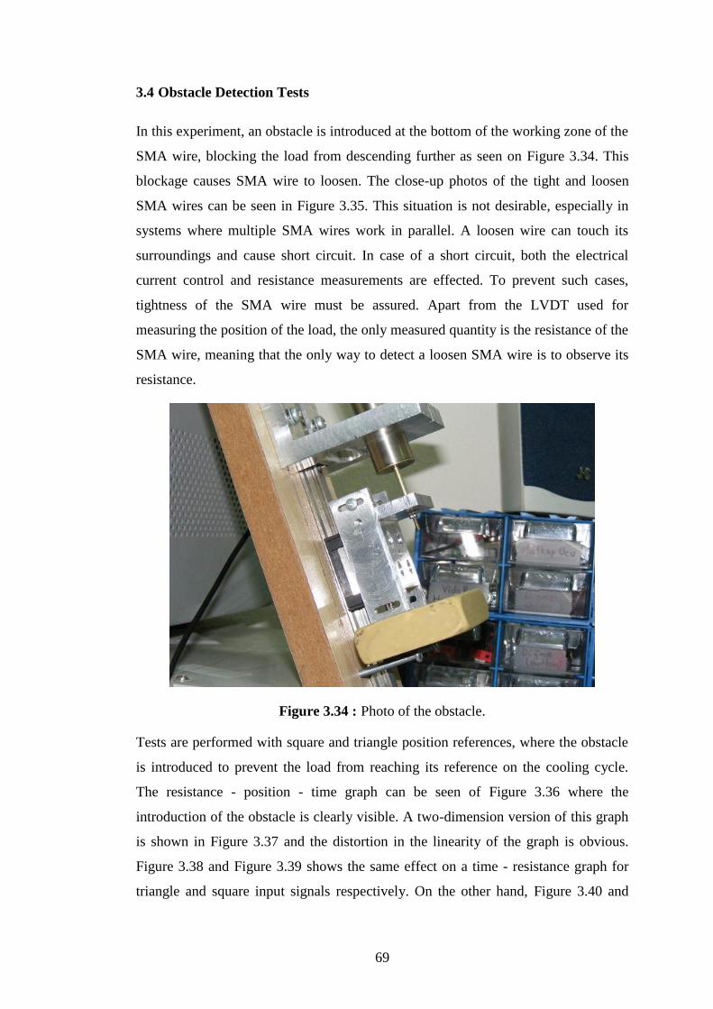
69
3.4 Obstacle Detection Tests
In this experiment, an obstacle is introduced at the bottom of the working zone of the
SMA wire, blocking the load from descending further as seen on Figure 3.34. This
blockage causes SMA wire to loosen. The close-up photos of the tight and loosen
SMA wires can be seen in Figure 3.35. This situation is not desirable, especially in
systems where multiple SMA wires work in parallel. A loosen wire can touch its
surroundings and cause short circuit. In case of a short circuit, both the electrical
current control and resistance measurements are effected. To prevent such cases,
tightness of the SMA wire must be assured. Apart from the LVDT used for
measuring the position of the load, the only measured quantity is the resistance of the
SMA wire, meaning that the only way to detect a loosen SMA wire is to observe its
resistance.
Figure 3.34 : Photo of the obstacle.
Tests are performed with square and triangle position references, where the obstacle
is introduced to prevent the load from reaching its reference on the cooling cycle.
The resistance - position - time graph can be seen of Figure 3.36 where the
introduction of the obstacle is clearly visible. A two-dimension version of this graph
is shown in Figure 3.37 and the distortion in the linearity of the graph is obvious.
Figure 3.38 and Figure 3.39 shows the same effect on a time - resistance graph for
triangle and square input signals respectively. On the other hand, Figure 3.40 and

70
Figure 3.41 shows the slopes of the time - resistance line and it is calculated in real
time by the LineFitter class. Again, the graph is smooth when no obstacle is
introduced in the cooling cycle, but high spikes can be seen when the obstacle is
present.
Figure 3.35 : Close-up photo of the (a) tight and (b) loosen SMA wire.
Figure 3.36 : Position - resistance - time graph with introduced obstacle.
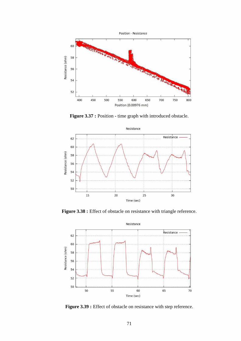
71
Figure 3.37 : Position - time graph with introduced obstacle.
Figure 3.38 : Effect of obstacle on resistance with triangle reference.
Figure 3.39 : Effect of obstacle on resistance with step reference.
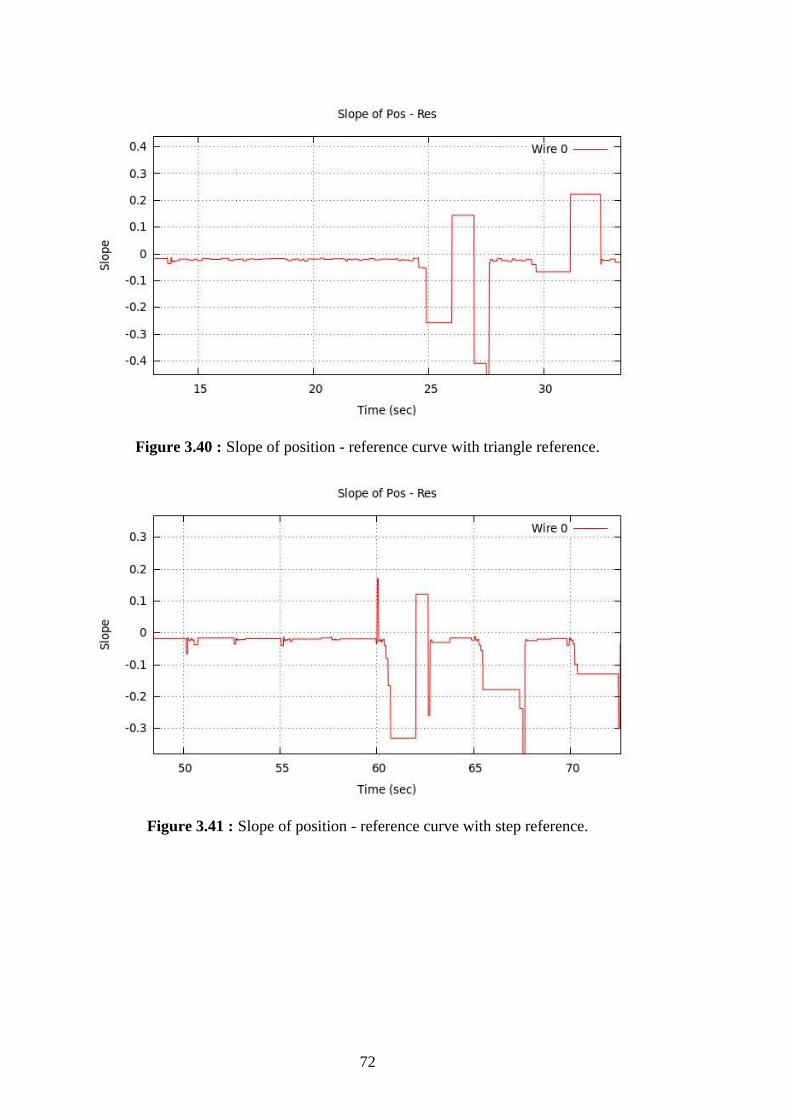
72
Figure 3.40 : Slope of position - reference curve with triangle reference.
Figure 3.41 : Slope of position - reference curve with step reference.
73
4. CONCLUSIONS AND RECOMMENDATIONS
4.1 Results and Comments
This study consists of two parts. The first part is the design and build process of the
experimental setup. The second part is the experiments performed with this
experimental setup.
During the design of the experimental setup, the data acquisition system, both the
hardware and software, is designed from scratch instead of using a readily available
data acquisition system. It is believed that, such an approach is more suitable as the
main goal of the study is to replace conventional actuators in robotic applications.
Although off-the-shelf DAQ systems are very time and cost effective for
experimental setups, it is hard to implement them in final actuator designs because of
their software and hardware dependencies. Unfortunately, designing a DAQ system
from the scratch is a time consuming task.
Despite the time cost of designing a DAQ system from scratch, this approach has
some advantages. A low cost DAQ card is designed and built. As its internal
software (firmware) is known, there are no unknown points in the execution of the
software. In addition, it is possible to tune the system according to the needs. Such a
system can be modified to be integrated into a larger system.
A computer software is designed to communicate with the DAQ card. This software
provides a graphical user interface for easy access to its controls. The software is
designed in an object oriented manner to improve modularity and extensibility. It is
possible to implement different control algorithms with no significant integration
effort. The software is also capable of showing the required internal variables on the
screen. These variables are also stored in log files for later inspection. The software
is designed in such a way that new variables can be easily added with a few lines of
code and they are automatically integrated into the GUI and logging system. Still,
there is a lot of work to do for reaching the desired level of modularity and
extensibility.

74
A SMA wire driver circuit is also designed and built as a part of the experimental
setup. This driver can control the current passing through the SMA wire. It is also
capable of measuring the voltage drop on the SMA wire allowing the calculation of
the resistance of the SMA wire. The SMA wire driver has an analog interface, which
provides early testing capabilities without the need of software. This card can also be
used with off-the-shelf DAQ systems, as most of them have analog input and output
channels.
During the experiments, it is observed that SMA wires show hysteretic behavior
during the heating and cooling cycles. This behavior can be easily seen on the graph
of open loop response to a sine wave current reference. Interestingly, the relation
between the strain and resistance of the SMA wires is almost linear.
For precise position control of SMA wires, the PID controller is tested. Coefficients
calculated with Ziegler - Nichols tuning methods does not give satisfactory results.
The operating zone where the tuning is applied affects the response of the SMA
wires and they do not perform well on operating zones other than the one they are
tuned in. A modification is applied to the integral term of the PID controller to make
KI inversely proportional to the error. This modification causes significant
improvements on the results.
Frequency responses of SMA wires with different diameters are also inspected. It is
observed that thin wires have larger bandwidth. It is concluded that thin wires are
more suitable for robotic applications because of their better frequency response
characteristics. It is also observed that the width of the operating zone affects the
frequency response. Wires perform better in narrow operating zones.
The effect of introducing an obstacle to prevent SMA to reach its desired position
during the cooling cycle is also tested. The obstacle causes SMA wire to be loosened,
which is not a desired situation. It is observed that, when the SMA wire is loosened,
the slope of the resistance - position graph changes. This can be used to prevent
wires to be loosened, which is believed to be essential if more than one parallel SMA
wires are to be used together in a tight arrangement, as a loosened wire can touch
other wires next to it and cause a short circuit.
75
4.2 Recommendations for Further Study
One of the major problems of the software running in the desktop computer is the
strict integration of the core and the GUI. The thread library used in the project also
depends on the GUI library. To improve the modularity and portability, the user
interface, graphical or command line, must be separated from the other parts of the
software. It is recommended that the interface and the core are run on different
threads. This gives the ability to run the core independently from the user interface.
Also, a socket based inter-process communication is recommended to run the user
interface process and the core process on different machines, which may be using
different architectures. This gives the ability to place the core in a low-end embedded
computer while the graphic supporting interface program can run on a desktop
computer. Also, this design makes it possible to change the interface program as
desired, provided that the same communication protocol is honored.
gnuplot, the graphing tool used in the visualization of collected data in the
experiments is very capable and easy to use with its command line interface.
However, it lacks the online data display ability, which severely cripples the
experimentation process. The current system supports only offline data visualization
in terms of graphs, where the online visualization of the data is available only in a
text based manner in the GUI of the software. The need of an interactive online
plotting tool is clear. The user should be able to watch the state of internal variables
during runtime by simply clicking on the graph.
One possible option for the software is the migration to ROS. ROS is an open-
source, meta-operating system for robots. It provides the services one would expect
from an operating system, including hardware abstraction, low-level device control,
implementation of commonly used functionality, message passing between
processes, and package management. It also provides tools and libraries for
obtaining, building, writing, and running code across multiple computers [28]. A
ROS program consists of individual sub-programs, called nodes. ROS handles the
communication and synchronization between the nodes. This provides great
modularity and extensibility. ROS nodes can also communicate over network, which
gives them the ability to run on different machines. ROS has a large community
support and many nodes are readily available for download and use. By the time of

76
this writing, ROS supports C++ and Python, but additional programming languages
are planned to be supported in the future.
As mentioned before, it may be a good idea to drive SMA wires digitally with PWM
signals, instead of analog components. This approach is not preferred during the
development cycle, as it complicates the measuring of the resistance. However, a
digital approach has the advantage of not requiring DAC modules, which are usually
not found on microcontrollers. Compact PCB designs are possible when they do not
include DAC modules. In addition, this approach can reduce the number of op-amps
required, which helps reducing the PCB size further.
During the experiments, it is observed that the SMA wires are highly sensitive to any
change temperature change in its surroundings. This situation makes it harder to
collect experimental data. However, the real problem is that, it makes impossible to
use SMA actuators in real working environments. It is clear that a mechanism against
such disturbances must be developed. The controller needs to be immune to such
disturbances. An artificial learning based adaptive controller is suggested as future
work.
Another future goal is determining the stress on each wire. Achieving this makes it
possible to design compliant systems actuated by SMA actuators without the need of
additional force sensors. This approach is similar to determining the torque applied
by electric motors by measuring their current consumption.
77
REFERENCES
[1] Shape-memory alloy (n.d.). In Wikipedia. Data retrieved: 17.12.2012, address:
http://en.wikipedia.org/wiki/Shape-memory_alloy
[2] Novotny, M., Kilpi, J. (n.d.). Shape Memory Alloys. Data retrieved: 17.12.2012,
address: http://www.ac.tut.fi/aci/courses/ACI-51106/pdf/SMA/SMA-
introduction.pdf
[3] Introduction to Shape Memory Alloys (n.d.). Data retrieved: 17.12.2012,
address: http://www.tinialloy.com/pdf/introductiontosma.pdf
[4] Sun, L., Huang, W., Ding, Z., Zhao, Y., Wang, C., Purnawali, H., Tang, C. (2012). Stimulus-responsive shape memory materials: A review,
Materials and Design, 33, 577-640.
[5] Falvo, A. (n.d). Thermomechanical characterization of Nickel-Titanium Shape
Memory Alloys.
[6] Joule Heating (n.d.). In Wikipedia. Data retrieved: 17.12.2012, address:
http://en.wikipedia.org/wiki/Joule_heating
[7] Odhner, L., Asada, H. (2006). Sensorless Temperature Estimation and Control
of Shape Memory Alloy Actuators Using Thermoelectric Devices,
IEEE/ASME Transactions on Mechatronics, vol. 11, no. 2.
[8] Kirkpatrick, K. (2009). Reinforcement Learning for Active Length Control and
Hysteresis Characterization of Shape Memory Alloys.
[9] Meier, H., Czechowicz, A. (2010). Concepts For Standardized Shape Memory
Actuators For Positioning Applications, Proceedings of the ASME
2010 Conference on Smart Materials, Adaptive Structures and
Intelligent Systems.
[10] Janaideh, M., Rkaheja, S., Su, C. (2008). Compensation of Hysteresis
Nonlinearities in Smart Actuators, ASME Conference on Smart
Materials, Adaptive Structures and Intelligent Systems.
[11] Sayyaadi, H., Zakerzadef, M. (2012). Position control of shape memory alloy
actuator based on the generalized Prandtl-Ishlinskii inverse model,
Mechatronics, 22, 945-957.
[12] Ahn, K., Kha, N. (2008). Modeling and control of shape memory alloy
actuators using Preisach model, genetic algorithm and fuzzy logic,
Mechatronics, 18, 141-158.
[13] Song, G., Chaudhry, V., Batur, C. (2003). Precision trancking control of
shape memory alloy actuators using neural networks and a sliding-
mode based robust controller, Smart Materials and Structures, 12,
223-231.
78
[14] Ma, N., Song, G., Lee, H. (2004). Position control of shape memory alloy
actuators with internal electrical resistance feedback using neural
networks, Smart Materials and Structures, 13, 777-783.
[15] Kirkpatrick, K., Valasek, J. (2009). Dimensionality Effects on the Markov
Property in Shape Memory Alloy Hysteretic Environment,
Proceedings of the 2009 IEEE International Conference on Systems,
Man, and Cybernetics.
[16] Gedouin, P., Delaleau, E., Bourgeot, J., Join, C., Chirani, S., Calloch, S.
(2011). Experimenral comparision of classical PID and model-free
control: Position control of a shape memory alloy active spring,
Control Engineering Practice, 19, 433-441.
[17] Ahola, J., Makkonen, T., Nevala, K., Isto, P. (2009). Comparison of Position
Control Algorithms of Embedded Shape Memory Alloy Actuators,
Proceedings of the 2009 IEEE International Conference on
Mechatronics.
[18] Dilibal, S., (2008). General Applications of NiTi Shape Memory Alloys.
[19] Urata, J., Yoshikai, T., Mizuuchi, I., Inaba, M. (2007). Design of High
D.O.F. Mobile Micro Robot Using Electrical Resistence Control of
Shape Memory Alloy, Proceedings of the 2007 IEEE/RSJ
International Conference on Intelligent Robots and Systems.
[20] Hangekar, R., Furst, S., Seelecke, S. (2010). Development of a 6-channel
Power Controller for Simultaneous Actuation and Resistance
Measurement of SMA Wires, Proceedings of ASME 2010 Conference
on Smart Materials, Adaptive Structures and Intelligent Systems.
[21] Heatsink of Swim (2011). Date retrieved: 17.12.2012, address:
http://www.nlvocables.com/blog/?p=697
[22] LM741 Datasheet (2004). Date retrieved: 17.12.2012, address:
http://www.ti.com/lit/ds/symlink/lm741.pdf
[23] Url-1 < http://www.picproje.org/index.php/topic,36102.msg259025.html#msg
259025>, Date retrieved: 17.12.2012.
[24] PIC18F2520 Datasheet (2008). Data retrieved: 17.12.2012, address:
http://ww1.microchip.com/downloads/en/DeviceDoc/39631E.pdf
[25] MCP4922 Datasheet (2004). Data retrieved: 17.12.2012, address:
http://ww1.microchip.com/downloads/en/devicedoc/21897a.pdf
[26] Thread (n.d.). In Wikipedia. Data retrieved: 17.12.2012, address:
http://en.wikipedia.org/wiki/Thread_(computing)
[27] Url-2 < http://linux.die.net/man/3/termios >, Data retrieved: 17.12.2012.
[28] ROS Introduction (2012). Data retrieved: 17.12.2012, address:
http://ros.org/wiki/ROS/Introduction
[29] Flexinol Actuator Wire Technical and Design Data (n.d.). Data retrieved:
17.12.2012, address: http://www.dynalloy.com/TechDataWire.php

79
APPENDICES
APPENDIX A: Initialization and Object Creation Sequence
APPENDIX B: PCB Designs
APPENDIX C: Additional Screenshots
APPENDIX D: Additional Tables

80
APPENDIX A
Creation of the MainFrame object.
Creation of the wxTimer object. Timer is not started yet.
Input from the user, indicating the serial port device and the controller of
choice.
Creation of the PidCtrl object (assumed to be chosen)
o Creation of the Controller object (the base class)
Creation of command and measured DataPack objects
Creation of input and output DPBuf objects which use the new
created command and measured DataPack objects as templates
Creation of Logger objects referencing the new created
DataPack objects
Creation of the SigGen object
Creation of LineFitter and Averager objects
o Creation of watch DataPack
o Creation of watch DPBuf object which uses new created watch
DataPack as template
Creation of PidCtrlPanel with the new created PidCtrl object
Creation of VarDisplays with previously created DPBuf objects
Addition of VarDisplay objects into the MainFrame
Creation of a new PicComm object
o Creation of a new SerialPort object
Start of wxTimer that was created before
Creation and start of PidCtrl thread

81
APPENDIX B
Figure B.1 : PCB design of the failed SMA driver.
Figure B.2 : PCB design of the integral controlled SMA driver.
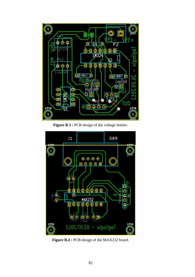
82
Figure B.3 : PCB design of the voltage limiter.
Figure B.4 : PCB design of the MAX232 board.

83
Figure B.5 : PCB design of the DAQ card.
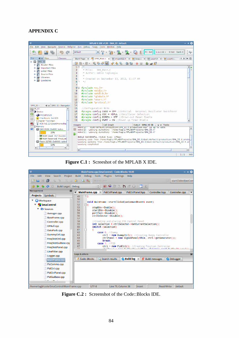
84
APPENDIX C
Figure C.1 : Screeshot of the MPLAB X IDE.
Figure C.2 : Screenshot of the Code::Blocks IDE.

85
Figure C.3 : Screenshot of the wxFormBuilder.
86
APPENDIX D
Table D.1 : Properties of Nitinol wires [29].
Diameter
Size
(mm)
Resistence
(ohms /
meter)
Pull Force
(grams)
Approximate
Current for 1
Second
Contraction
Cooling
Time for
70C Wire
(seconds)
Cooling
Time fır
90C Wire
(seconds)
0.025 1425 8.9 45 0.18 0.15
0.038 890 20 55 0.24 0.20
0.050 500 36 85 0.4 0.3
0.076 232 80 150 0.8 0.7
0.10 126 143 200 1.1 0.9
0.13 75 223 320 1.6 1.4
0.15 55 321 410 2.0 1.7
0.20 29 570 660 3.2 2.7
0.25 18.5 891 1050 5.4 4.5
0.31 12.2 1280 1500 8.1 6.8
0.38 8.3 2250 2250 10.5 8.8
0.51 4.3 3560 4000 16.8 14.0

87
CURRICULUM VITAE
Name Surname: Gökçe Burak Tağlıoğlu
Place and Date of Birth: Adana - 21.06.1987
E-Mail: [email protected]
B.Sc.: Marmara University - Mechanical Engineering