issn 1348-6535 coden:jcsjew jcs japan
TRANSCRIPT

JCS-Japan第126巻 第 9 号 平成30年 9 月 1 日発行(毎月1回1日発行) ISSN 1348-6535 CODEN: JCSJEW
September
2018
vol.126
Journal of the Ceramic Society of Japan

SPECIAL ARTICLE
The 72th CerSJ Awards for Advancements in Ceramic Science and Technology: Review
Ferroelectricity in HfO2 and related ferroelectrics
Takao SHIMIZU1,³
1School of Materials and Chemical Technology, Tokyo Institute of Technology, 4259 Nagatsuta, Midori, Yokohama 226–8502, Japan
Ferroelectric HfO2 film has garnered a lot of attention lately due to unique features that cannot be achieved withconventional ferroelectric materials. The ferroelectricity of HfO2 originates from the metastable orthorhombicphase, which does not appear in the phase transition sequence of HfO2 in ambient pressure. This reviewintroduces our recent research on HfO2-related ferroelectrics. The ferroelectric orthorhombic phase wasachieved with Hf0.5Zr0.5O2 metalorganic chemical vapor deposition, and obtained by intermediate thermaltreatment conditions with low- and high-thermal budget yield in the tetragonal and monoclinic phases,respectively. Furthermore, ferroelectricity was enhanced with the aid of compressive strain, as elucidated by astudy using various substrates with different thermal expansion coefficients. Epitaxial films were successfullygrown by quenching of a YO1.5HfO2 solid solution. This epitaxial film revealed that HfO2-related ferroelectricsare good candidates for future integrated application because their ferroelectric properties are comparable toconventional ferroelectric materials.©2018 The Ceramic Society of Japan. All rights reserved.
Key-words : Ferroelectricity, Thin films, Hafnium oxides
[Received May 21, 2018; Accepted July 3, 2018]
1. Introduction
Ferroelectric materials are one of the most importantelectroceramic materials because of their outstandingdielectric properties and electromechanical responses.1)3)
It is no exaggeration to say that perovskite-type ferro-electrics and related materials are currently the focus ofintense interest in both the industrial and scientific fields.However, it is widely recognized that perovskite materialsshow deterioration with downsizing, decreasing particlesize, or film thickness. This serious issue makes it difficultto process them into integrated devices.4) In particular, theincompatibility of perovskite-type ferroelectrics with semi-conductor technologies has not been surmounted, andas yet there are a few applications that use ferroelectricthin films. Nevertheless, novel ferroelectric devices suchas ferroelectric tunnel junctions,5),6) piezotoronic transis-tors,7),8) and negative capacitance transistors9),10) are ofinterest. Therefore new ferroelectric materials that areproof against scaling (i.e., have high compatibility withsemiconductor technologies) are in high demand.
HfO2 ferroelectric materials have been reported byBöscke et al.11) The most remarkable features of thesematerials are their simple chemical composition andthermodynamic stability, which lead to high compatibilitywith Si-based semiconductor technology.12),13) HfO2-based
materials are, indeed, utilized as dielectric layers instead ofconventional silicon oxides layers in current field-effecttransistors due to their higher dielectric constant.14)16) Thismeans mature fabrication processes are available for highlyintegrated ferroelectric devices using ferroelectric HfO2
materials. Several pioneering demonstrations of ferro-electric devices for both capacitor-type ferroelectric mem-ories and ferroelectric field-effect transistors have beenreported.17)19) In addition, recent intensive studies haverevealed novel ferroelectric applications, such as ferroelec-tric tunnel junctions,20)23) a tunable capacitor,24),25) electro-static energy storage devices,26)30) and so on.31)33)
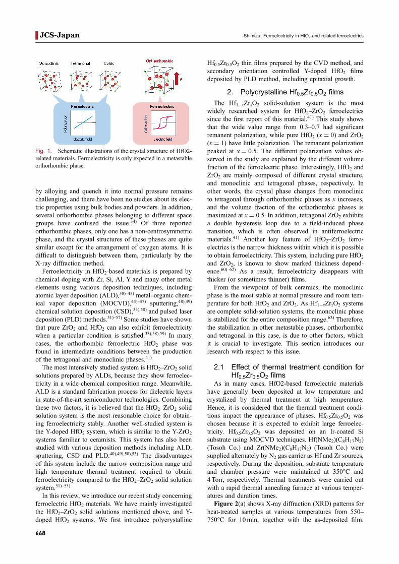
In general, ferroelectricity is in many cases associatedby structural phase transition to a lower symmetric polarphase from a higher symmetric polar phase (it is generallydifficult to switch polarization of materials without a phasetransition by external electric field). The ferroelectricity inHfO2 (and ZrO2) stems from the polar (and of course non-centrosymmetric) orthorhombic phases (see Fig. 1). ZrO2
and HfO2 undergo successive structural phase transitions.The monoclinic baddeleyite, tetragonal, and cubic fluoritephases shown in Fig. 1, which appear by the successivephase transitions, have been well studied. They have aninversion center that does not show ferroelectricity.On the other hand, the orthorhombic phase in ZrO2 and
HfO2 is less studied. This phase in ZrO2 and HfO2 isknown to be produced by chemical substitution with MgO,CaO, and Y2O3, or by exposure in ambient high pres-sure.34)37) However, obtaining a pure orthorhombic phase
³ Corresponding author: T. Shimizu; E-mail: [email protected]
Journal of the Ceramic Society of Japan 126 [9] 667-674 2018
DOI http://doi.org/10.2109/jcersj2.18104 JCS-Japan
©2018 The Ceramic Society of Japan 667
by alloying and quench it into normal pressure remainschallenging, and there have been no studies about its elec-tric properties using bulk bodies and powders. In addition,several orthorhombic phases belonging to different spacegroups have confused the issue.34) Of three reportedorthorhombic phases, only one has a non-centrosymmetricphase, and the crystal structures of these phases are quitesimilar except for the arrangement of oxygen atoms. It isdifficult to distinguish between them, particularly by theX-ray diffraction method.
Ferroelectricity in HfO2-based materials is prepared bychemical doping with Zr, Si, Al, Y and many other metalelements using various deposition techniques, includingatomic layer deposition (ALD),38)43) metalorganic chem-ical vapor deposition (MOCVD),44)47) sputtering,48),49)
chemical solution deposition (CSD),33),50) and pulsed laserdeposition (PLD) methods.51)57) Some studies have shownthat pure ZrO2 and HfO2 can also exhibit ferroelectricitywhen a particular condition is satisfied.33),58),59) In manycases, the orthorhombic ferroelectric HfO2 phase wasfound in intermediate conditions between the productionof the tetragonal and monoclinic phases.41)
The most intensively studied system is HfO2ZrO2 solidsolutions prepared by ALDs, because they show ferroelec-tricity in a wide chemical composition range. Meanwhile,ALD is a standard fabrication process for dielectric layersin state-of-the-art semiconductor technologies. Combiningthese two factors, it is believed that the HfO2ZrO2 solidsolution system is the most reasonable choice for obtain-ing ferroelectricity stably. Another well-studied system isthe Y-doped HfO2 system, which is similar to the Y-ZrO2
systems familiar to ceramists. This system has also beenstudied with various deposition methods including ALD,sputtering, CSD and PLD.40),49),50),53) The disadvantagesof this system include the narrow composition range andhigh temperature thermal treatment required to obtainferroelectricity compared to the HfO2ZrO2 solid solutionsystem.51)53)
In this review, we introduce our recent study concerningferroelectric HfO2 materials. We have mainly investigatedthe HfO2ZrO2 solid solutions mentioned above, and Y-doped HfO2 systems. We first introduce polycrystalline
Hf0.5Zr0.5O2 thin films prepared by the CVD method, andsecondary orientation controlled Y-doped HfO2 filmsdeposited by PLD method, including epitaxial growth.
2. Polycrystalline Hf0.5Zr0.5O2 films
The Hf1¹xZrxO2 solid-solution system is the mostwidely researched system for HfO2ZrO2 ferroelectricssince the first report of this material.41) This study showsthat the wide value range from 0.30.7 had significantremanent polarization, while pure HfO2 (x = 0) and ZrO2
(x = 1) have little polarization. The remanent polarizationpeaked at x = 0.5. The different polarization values ob-served in the study are explained by the different volumefraction of the ferroelectric phase. Interestingly, HfO2 andZrO2 are mainly composed of different crystal structure,and monoclinic and tetragonal phases, respectively. Inother words, the crystal phase changes from monoclinicto tetragonal through orthorhombic phases as x increases,and the volume fraction of the orthorhombic phases ismaximized at x = 0.5. In addition, tetragonal ZrO2 exhibitsa double hysteresis loop due to a field-induced phasetransition, which is often observed in antiferroelectricmaterials.41) Another key feature of HfO2ZrO2 ferro-electrics is the narrow thickness within which it is possibleto obtain ferroelectricity. This system, including pure HfO2
and ZrO2, is known to show marked thickness depend-ence.60)62) As a result, ferroelectricity disappears withthicker (or sometimes thinner) films.From the viewpoint of bulk ceramics, the monoclinic
phase is the most stable at normal pressure and room tem-perature for both HfO2 and ZrO2. As Hf1¹xZrxO2 systemsare complete solid-solution systems, the monoclinic phaseis stabilized for the entire composition range.63) Therefore,the stabilization in other metastable phases, orthorhombicand tetragonal in this case, is due to other factors, whichit is crucial to investigate. This section introduces ourresearch with respect to this issue.
2.1 Effect of thermal treatment condition forHf0.5Zr0.5O2 films
As in many cases, HfO2-based ferroelectric materialshave generally been deposited at low temperature andcrystalized by thermal treatment at high temperature.Hence, it is considered that the thermal treatment condi-tions impact the appearance of phases. Hf0.5Zr0.5O2 waschosen because it is expected to exhibit large ferroelec-tricity. Hf0.5Zr0.5O2 was deposited on an Ir-coated Sisubstrate using MOCVD techniques. Hf(NMe2)(C8H17N2)(Tosoh Co.) and Zr(NMe2)(C8H17N2) (Tosoh Co.) weresupplied alternately by N2 gas carrier as Hf and Zr sources,respectively. During the deposition, substrate temperatureand chamber pressure were maintained at 350°C and4Torr, respectively. Thermal treatments were carried outwith a rapid thermal annealing furnace at various temper-atures and duration times.Figure 2(a) shows X-ray diffraction (XRD) patterns for
heat-treated samples at various temperatures from 550750°C for 10min, together with the as-deposited film.
Fig. 1. Schematic illustrations of the crystal structure of HfO2-related materials. Ferroelectricity is only expected in a metastableorthorhombic phase.
Shimizu: Ferroelectricity in HfO2 and related ferroelectricsJCS-Japan
668

Grazing incidence X-ray diffraction (GIXRD) was em-ployed to acquire diffractograms. The XRD pattern for theas-deposited film shows no clear peaks, suggesting thatthe film was amorphous. The XRD pattern for the filmtreated at the lowest temperature of 550°C shows thatfilm was sufficiently crystalized even at this temperature.The strongest peak at around 30.9° is attributed to theorthorhombic or tetragonal 111 peak (note that doubledcells are employed here for ease of understanding), whilethat at around 31.6° is ascribed to the monoclinic phase.The peak from the monoclinic phase becomes muchstronger with an increase in treatment temperature. Inaddition, the peak from the orthorhombic and tetragonalphases shifted toward lower angles as treatment temper-ature increased.
The 111 lattice spacing of the orthorhombic phase islarger than that of the tetragonal phase according to aprevious study,41),64) and this peak shift indicates the phasechange from tetragonal to orthorhombic phase. Figure 2(b)shows the treatment temperature dependence of the PEhysteresis loop. Films treated at 650°C showed the largestremanent polarization of around 12¯C/cm2. This treatedtemperature dependence may be understood by consid-ering the following. Deposited film crystalizes in thetetragonal phase, and finally transforms to the most stablemonoclinic phase. The orthorhombic phase appears as theintermediate state between the initial tetragonal nuclei andthe stable monoclinic grain. Similar results were obtainedby changing treatment duration at the fixed temperature of650°C. In that case, shorter duration yielded the tetragonalphase and longer duration the monoclinic phase, whileintermediate duration produced the orthorhombic phasewith the largest remanent polarization. Note that the tetrag-onal and monoclinic phases are known to have the highestand lowest dielectric constant, respectively. Thus, thedielectric constant tends to decrease with the increase inthermal budget. Figure 3 schematizes the process of thethermal treatment.
It should be pointed out that the constituent phases ofthe Hf1¹xZrxO2 films strongly depend on particle size from
both an experimental and theoretical viewpoint.65)67) Thiseffect is explained by the difference in surface energy,which is an additional term of free energy. In a previousstudy for small particle ZrO2,68),69) the crystal phase wasfound to change to a higher symmetry phase such as thetetragonal phase. Our study follows this scenario; i.e., theprogress of the crystallization produces the growing parti-cle size, changing the stability of the crystal phases. Theferroelectric phase appears as an intermediate state.
2.2 Strain effect for Hf0.5Zr0.5O2 filmsCapping and annealing, which is the thermal treatment
for the sandwiched film by top and bottom electrodes, areoften utilized to obtain ferroelectricity in HfO2-basedmaterials, since mechanical encapsulation is reported tosuppress the generation of the monoclinic phase.11),41),42)
This means that one can take advantage of mechanical
Fig. 2. (a) A thermal treatment temperature evolution of XRD patterns for MOCVD deposited Hf1¹xZrxO2 filmstogether with an as-deposited film. (b) PE hysteresis loop measured on the film treated at various temper-atures.45) Copyright 2014, The Japan Society of Applied Physics.
Fig. 3. Summary of the relation between crystal structure,dielectric properties, and annealing condition.
Journal of the Ceramic Society of Japan 126 [9] 667-674 2018 JCS-Japan
669
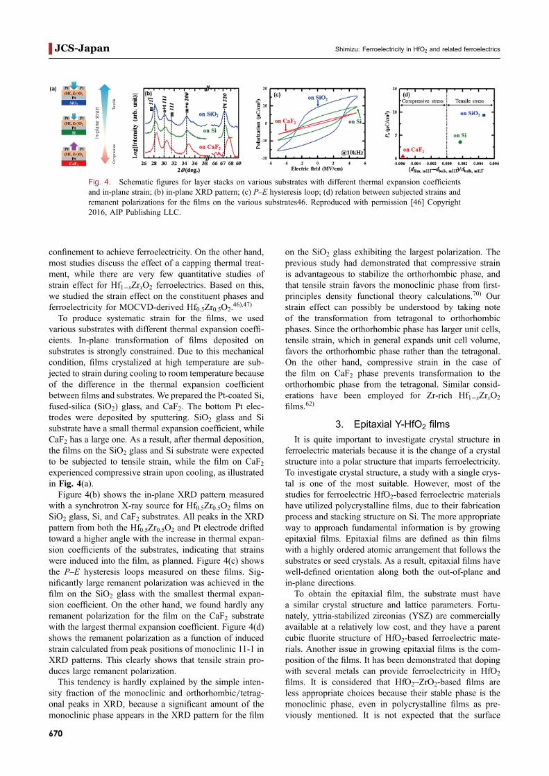
confinement to achieve ferroelectricity. On the other hand,most studies discuss the effect of a capping thermal treat-ment, while there are very few quantitative studies ofstrain effect for Hf1¹xZrxO2 ferroelectrics. Based on this,we studied the strain effect on the constituent phases andferroelectricity for MOCVD-derived Hf0.5Zr0.5O2.46),47)
To produce systematic strain for the films, we usedvarious substrates with different thermal expansion coeffi-cients. In-plane transformation of films deposited onsubstrates is strongly constrained. Due to this mechanicalcondition, films crystalized at high temperature are sub-jected to strain during cooling to room temperature becauseof the difference in the thermal expansion coefficientbetween films and substrates. We prepared the Pt-coated Si,fused-silica (SiO2) glass, and CaF2. The bottom Pt elec-trodes were deposited by sputtering. SiO2 glass and Sisubstrate have a small thermal expansion coefficient, whileCaF2 has a large one. As a result, after thermal deposition,the films on the SiO2 glass and Si substrate were expectedto be subjected to tensile strain, while the film on CaF2experienced compressive strain upon cooling, as illustratedin Fig. 4(a).
Figure 4(b) shows the in-plane XRD pattern measuredwith a synchrotron X-ray source for Hf0.5Zr0.5O2 films onSiO2 glass, Si, and CaF2 substrates. All peaks in the XRDpattern from both the Hf0.5Zr0.5O2 and Pt electrode driftedtoward a higher angle with the increase in thermal expan-sion coefficients of the substrates, indicating that strainswere induced into the film, as planned. Figure 4(c) showsthe PE hysteresis loops measured on these films. Sig-nificantly large remanent polarization was achieved in thefilm on the SiO2 glass with the smallest thermal expan-sion coefficient. On the other hand, we found hardly anyremanent polarization for the film on the CaF2 substratewith the largest thermal expansion coefficient. Figure 4(d)shows the remanent polarization as a function of inducedstrain calculated from peak positions of monoclinic 11-1 inXRD patterns. This clearly shows that tensile strain pro-duces large remanent polarization.
This tendency is hardly explained by the simple inten-sity fraction of the monoclinic and orthorhombic/tetrag-onal peaks in XRD, because a significant amount of themonoclinic phase appears in the XRD pattern for the film
on the SiO2 glass exhibiting the largest polarization. Theprevious study had demonstrated that compressive strainis advantageous to stabilize the orthorhombic phase, andthat tensile strain favors the monoclinic phase from first-principles density functional theory calculations.70) Ourstrain effect can possibly be understood by taking noteof the transformation from tetragonal to orthorhombicphases. Since the orthorhombic phase has larger unit cells,tensile strain, which in general expands unit cell volume,favors the orthorhombic phase rather than the tetragonal.On the other hand, compressive strain in the case ofthe film on CaF2 phase prevents transformation to theorthorhombic phase from the tetragonal. Similar consid-erations have been employed for Zr-rich Hf1¹xZrxO2
films.62)
3. Epitaxial Y-HfO2 films
It is quite important to investigate crystal structure inferroelectric materials because it is the change of a crystalstructure into a polar structure that imparts ferroelectricity.To investigate crystal structure, a study with a single crys-tal is one of the most suitable. However, most of thestudies for ferroelectric HfO2-based ferroelectric materialshave utilized polycrystalline films, due to their fabricationprocess and stacking structure on Si. The more appropriateway to approach fundamental information is by growingepitaxial films. Epitaxial films are defined as thin filmswith a highly ordered atomic arrangement that follows thesubstrates or seed crystals. As a result, epitaxial films havewell-defined orientation along both the out-of-plane andin-plane directions.To obtain the epitaxial film, the substrate must have
a similar crystal structure and lattice parameters. Fortu-nately, yttria-stabilized zirconias (YSZ) are commerciallyavailable at a relatively low cost, and they have a parentcubic fluorite structure of HfO2-based ferroelectric mate-rials. Another issue in growing epitaxial films is the com-position of the films. It has been demonstrated that dopingwith several metals can provide ferroelectricity in HfO2
films. It is considered that HfO2ZrO2-based films areless appropriate choices because their stable phase is themonoclinic phase, even in polycrystalline films as pre-viously mentioned. It is not expected that the surface
Fig. 4. Schematic figures for layer stacks on various substrates with different thermal expansion coefficientsand in-plane strain; (b) in-plane XRD pattern; (c) PE hysteresis loop; (d) relation between subjected strains andremanent polarizations for the films on the various substrates46. Reproduced with permission [46] Copyright2016, AIP Publishing LLC.
Shimizu: Ferroelectricity in HfO2 and related ferroelectricsJCS-Japan
670
energy will be helpful, because epitaxial film has smallerinterfaces than polycrystalline film, which has more grainat the boundary.
We therefore selected YO1.5 substituted HfO2 systems,because the ferroelectricity in these has been achieved byvarious deposition techniques.40),49),50),53) In addition, it hasbeen reported that the orthorhombic phase was achievedusing quenched powder from arc-melt solvent, althoughthere was no discussion of ferroelectricity.71) It is knownthat the YO1.5HfO2 pseudo binary system is not a com-plete solid-solution system, but shows the wide phasecoexistence region as an analogue to well-known YO1.5ZrO2 systems. Our assumption was that the quenchingsolid solution might produce an orthorhombic ferroelectricphase by the growth of thin film, epitaxial film in this case,which is known to make solid solution over the solubilitylimit.72),73)
Epitaxial YO1.5 substituted HfO2 films were grownusing the PLD method on (110) YSZ substrate. Handmade7% YO1.5 substituted HfO2 (YHO-7) ceramics were usedas the target materials. Before deposition of YHO-7, wegrew Sn-doped In2O3 (ITO) as a bottom electrode, whichwas reported to be grown epitaxially on an YSZ substrate.An (110) YSZ substrate was chosen because YHO-7 filmstend to grow along the non-polar direction on the (100)YSZ substrate with an ITO layer.
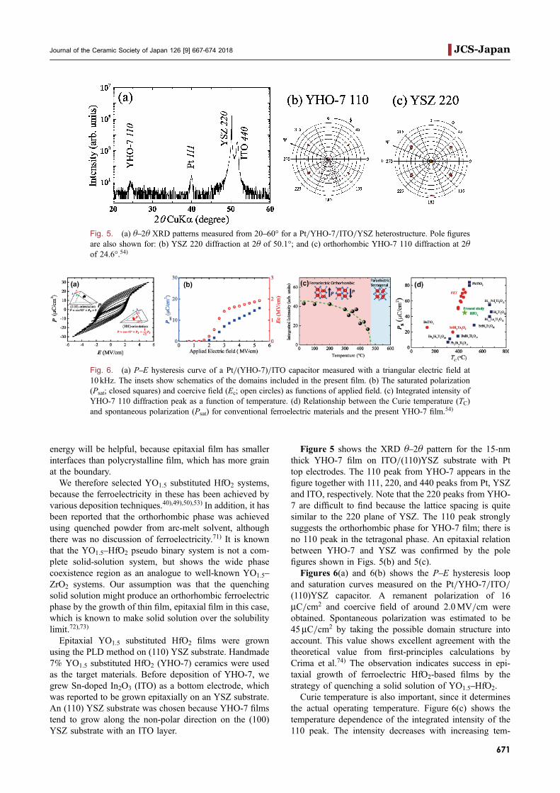
Figure 5 shows the XRD ª2ª pattern for the 15-nmthick YHO-7 film on ITO/(110)YSZ substrate with Pttop electrodes. The 110 peak from YHO-7 appears in thefigure together with 111, 220, and 440 peaks from Pt, YSZand ITO, respectively. Note that the 220 peaks from YHO-7 are difficult to find because the lattice spacing is quitesimilar to the 220 plane of YSZ. The 110 peak stronglysuggests the orthorhombic phase for YHO-7 film; there isno 110 peak in the tetragonal phase. An epitaxial relationbetween YHO-7 and YSZ was confirmed by the polefigures shown in Figs. 5(b) and 5(c).Figures 6(a) and 6(b) shows the PE hysteresis loop
and saturation curves measured on the Pt/YHO-7/ITO/(110)YSZ capacitor. A remanent polarization of 16¯C/cm2 and coercive field of around 2.0MV/cm wereobtained. Spontaneous polarization was estimated to be45¯C/cm2 by taking the possible domain structure intoaccount. This value shows excellent agreement with thetheoretical value from first-principles calculations byCrima et al.74) The observation indicates success in epi-taxial growth of ferroelectric HfO2-based films by thestrategy of quenching a solid solution of YO1.5HfO2.Curie temperature is also important, since it determines
the actual operating temperature. Figure 6(c) shows thetemperature dependence of the integrated intensity of the110 peak. The intensity decreases with increasing tem-
Fig. 5. (a) ª2ª XRD patterns measured from 2060° for a Pt/YHO-7/ITO/YSZ heterostructure. Pole figuresare also shown for: (b) YSZ 220 diffraction at 2ª of 50.1°; and (c) orthorhombic YHO-7 110 diffraction at 2ªof 24.6°.54)
Fig. 6. (a) PE hysteresis curve of a Pt/(YHO-7)/ITO capacitor measured with a triangular electric field at10 kHz. The insets show schematics of the domains included in the present film. (b) The saturated polarization(Psat; closed squares) and coercive field (Ec; open circles) as functions of applied field. (c) Integrated intensity ofYHO-7 110 diffraction peak as a function of temperature. (d) Relationship between the Curie temperature (TC)and spontaneous polarization (Psat) for conventional ferroelectric materials and the present YHO-7 film.54)
Journal of the Ceramic Society of Japan 126 [9] 667-674 2018 JCS-Japan
671
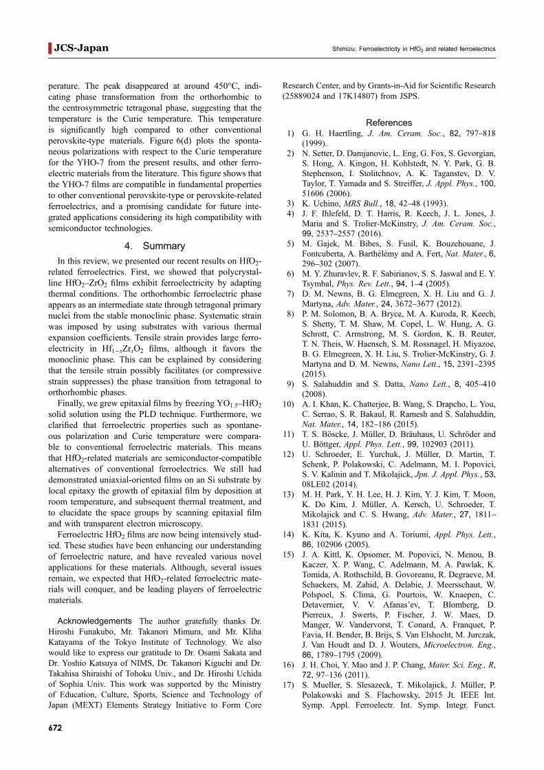
perature. The peak disappeared at around 450°C, indi-cating phase transformation from the orthorhombic tothe centrosymmetric tetragonal phase, suggesting that thetemperature is the Curie temperature. This temperatureis significantly high compared to other conventionalperovskite-type materials. Figure 6(d) plots the sponta-neous polarizations with respect to the Curie temperaturefor the YHO-7 from the present results, and other ferro-electric materials from the literature. This figure shows thatthe YHO-7 films are compatible in fundamental propertiesto other conventional perovskite-type or perovskite-relatedferroelectrics, and a promising candidate for future inte-grated applications considering its high compatibility withsemiconductor technologies.
4. Summary
In this review, we presented our recent results on HfO2-related ferroelectrics. First, we showed that polycrystal-line HfO2ZrO2 films exhibit ferroelectricity by adaptingthermal conditions. The orthorhombic ferroelectric phaseappears as an intermediate state through tetragonal primarynuclei from the stable monoclinic phase. Systematic strainwas imposed by using substrates with various thermalexpansion coefficients. Tensile strain provides large ferro-electricity in Hf1¹xZrxO2 films, although it favors themonoclinic phase. This can be explained by consideringthat the tensile strain possibly facilitates (or compressivestrain suppresses) the phase transition from tetragonal toorthorhombic phases.
Finally, we grew epitaxial films by freezing YO1.5HfO2
solid solution using the PLD technique. Furthermore, weclarified that ferroelectric properties such as spontane-ous polarization and Curie temperature were compara-ble to conventional ferroelectric materials. This meansthat HfO2-related materials are semiconductor-compatiblealternatives of conventional ferroelectrics. We still haddemonstrated uniaxial-oriented films on an Si substrate bylocal epitaxy the growth of epitaxial film by deposition atroom temperature, and subsequent thermal treatment, andto elucidate the space groups by scanning epitaxial filmand with transparent electron microscopy.
Ferroelectric HfO2 films are now being intensively stud-ied. These studies have been enhancing our understandingof ferroelectric nature, and have revealed various novelapplications for these materials. Although, several issuesremain, we expected that HfO2-related ferroelectric mate-rials will conquer, and be leading players of ferroelectricmaterials.
Acknowledgements The author gratefully thanks Dr.Hiroshi Funakubo, Mr. Takanori Mimura, and Mr. KlihaKatayama of the Tokyo Institute of Technology. We alsowould like to express our gratitude to Dr. Osami Sakata andDr. Yoshio Katsuya of NIMS, Dr. Takanori Kiguchi and Dr.Takahisa Shiraishi of Tohoku Univ., and Dr. Hiroshi Uchidaof Sophia Univ. This work was supported by the Ministryof Education, Culture, Sports, Science and Technology ofJapan (MEXT) Elements Strategy Initiative to Form Core
Research Center, and by Grants-in-Aid for Scientific Research(25889024 and 17K14807) from JSPS.
References1) G. H. Haertling, J. Am. Ceram. Soc., 82, 797818
(1999).2) N. Setter, D. Damjanovic, L. Eng, G. Fox, S. Gevorgian,
S. Hong, A. Kingon, H. Kohlstedt, N. Y. Park, G. B.Stephenson, I. Stolitchnov, A. K. Taganstev, D. V.Taylor, T. Yamada and S. Streiffer, J. Appl. Phys., 100,51606 (2006).
3) K. Uchino, MRS Bull., 18, 4248 (1993).4) J. F. Ihlefeld, D. T. Harris, R. Keech, J. L. Jones, J.
Maria and S. Trolier-McKinstry, J. Am. Ceram. Soc.,99, 25372557 (2016).
5) M. Gajek, M. Bibes, S. Fusil, K. Bouzehouane, J.Fontcuberta, A. Barthélémy and A. Fert, Nat. Mater., 6,296302 (2007).
6) M. Y. Zhuravlev, R. F. Sabirianov, S. S. Jaswal and E. Y.Tsymbal, Phys. Rev. Lett., 94, 14 (2005).
7) D. M. Newns, B. G. Elmegreen, X. H. Liu and G. J.Martyna, Adv. Mater., 24, 36723677 (2012).
8) P. M. Solomon, B. A. Bryce, M. A. Kuroda, R. Keech,S. Shetty, T. M. Shaw, M. Copel, L. W. Hung, A. G.Schrott, C. Armstrong, M. S. Gordon, K. B. Reuter,T. N. Theis, W. Haensch, S. M. Rossnagel, H. Miyazoe,B. G. Elmegreen, X. H. Liu, S. Trolier-McKinstry, G. J.Martyna and D. M. Newns, Nano Lett., 15, 23912395(2015).
9) S. Salahuddin and S. Datta, Nano Lett., 8, 405410(2008).
10) A. I. Khan, K. Chatterjee, B. Wang, S. Drapcho, L. You,C. Serrao, S. R. Bakaul, R. Ramesh and S. Salahuddin,Nat. Mater., 14, 182186 (2015).
11) T. S. Böscke, J. Müller, D. Bräuhaus, U. Schröder andU. Böttger, Appl. Phys. Lett., 99, 102903 (2011).
12) U. Schroeder, E. Yurchuk, J. Müller, D. Martin, T.Schenk, P. Polakowski, C. Adelmann, M. I. Popovici,S. V. Kalinin and T. Mikolajick, Jpn. J. Appl. Phys., 53,08LE02 (2014).
13) M. H. Park, Y. H. Lee, H. J. Kim, Y. J. Kim, T. Moon,K. Do Kim, J. Müller, A. Kersch, U. Schroeder, T.Mikolajick and C. S. Hwang, Adv. Mater., 27, 18111831 (2015).
14) K. Kita, K. Kyuno and A. Toriumi, Appl. Phys. Lett.,86, 102906 (2005).
15) J. A. Kittl, K. Opsomer, M. Popovici, N. Menou, B.Kaczer, X. P. Wang, C. Adelmann, M. A. Pawlak, K.Tomida, A. Rothschild, B. Govoreanu, R. Degraeve, M.Schaekers, M. Zahid, A. Delabie, J. Meersschaut, W.Polspoel, S. Clima, G. Pourtois, W. Knaepen, C.Detavernier, V. V. Afanas’ev, T. Blomberg, D.Pierreux, J. Swerts, P. Fischer, J. W. Maes, D.Manger, W. Vandervorst, T. Conard, A. Franquet, P.Favia, H. Bender, B. Brijs, S. Van Elshocht, M. Jurczak,J. Van Houdt and D. J. Wouters, Microelectron. Eng.,86, 17891795 (2009).
16) J. H. Choi, Y. Mao and J. P. Chang, Mater. Sci. Eng., R,72, 97136 (2011).
17) S. Mueller, S. Slesazeck, T. Mikolajick, J. Müller, P.Polakowski and S. Flachowsky, 2015 Jt. IEEE Int.Symp. Appl. Ferroelectr. Int. Symp. Integr. Funct.
Shimizu: Ferroelectricity in HfO2 and related ferroelectricsJCS-Japan
672

Piezoelectric Force Microsc. Work. ISAF/ISIF/PFM2015 233236 (2015).
18) J. Muller, P. Polakowski, S. Mueller and T. Mikolajick,ECS J. Solid State Sci. Technol., 4, N30N35 (2015).
19) H. Mulaos, J. O. Ker, S. Mulle, U. Schroeder, J. Müller,P. Polakowski, S. Flachowsky, R. Van Bentum, T.Mikolajick and S. Slesazeck, ACS Appl. Mater. Inter-faces, 9, 37923798 (2017).
20) M. Yamaguchi, S. Fujii, Y. Kamimuta, S. Kabuyanagi,T. Ino, Y. Nakasaki, R. Takaishi, R. Ichihara and M.Saitoh, IEEE Int. Reliab. Phys. Symp., 2, 16 (2018).
21) X. Tian and A. Toriumi, 2017 IEEE Electron DevicesTechnol. Manuf. Conf. Proc. Tech. 45 (2017).
22) F. Ambriz-Vargas, G. Kolhatkar, M. Broyer, A. Hadj-Youssef, R. Nouar, A. Sarkissian, R. Thomas, C.Gomez-Yáñez, M. A. Gauthier and A. Ruediger, ACSAppl. Mater. Interfaces, 9, 1326213268 (2017).
23) Z. Xi, C. Zheng and Z. Wen, ACS Appl. Mater.Interfaces, 10, 60246030 (2018).
24) M. Dragoman, M. Modreanu, I. M. Povey, S.Iordanescu, M. Aldrigo, C. Romanitan, D. Vasilache,A. Dinescu and D. Dragoman, Nanotechnology, 28,38LT04 (2017).
25) M. Dragoman, M. Aldrigo, M. Modreanu and D.Dragoman, Appl. Phys. Lett., 110, 15 (2017).
26) M. H. Park, H. J. Kim, Y. J. Kim, T. Moon, K. Do Kimand C. S. Hwang, Adv. Energy Mater., 4, 1400610(2014).
27) M. H. Park, H. J. Kim, Y. J. Kim, T. Moon, K. Do Kimand C. S. Hwang, Phys. Status Solidi RRL, 8, 857861(2014).
28) F. Ali, X. Liu, D. Zhou, X. Yang, J. Xu, T. Schenk, J.Müller, U. Schroeder, F. Cao and X. Dong, J. Appl.Phys., 122, 144105 (2017).
29) M. H. Park, T. Schenk, M. Hoffmann, S. Knebel, J.Gärtner, T. Mikolajick and U. Schroeder, Nano Energy,36, 381389 (2017).
30) K. Do Kim, Y. H. Lee, T. Gwon, Y. J. Kim, H. J. Kim, T.Moon, S. D. Hyun, H. W. Park, M. H. Park and C. S.Hwang, Nano Energy, 39, 390399 (2017).
31) M. Pešić, M. Hoffmann, C. Richter, T. Mikolajick andU. Schroeder, Adv. Funct. Mater., 26, 74867494(2016).
32) M. Hoffmann, M. Pešić, K. Chatterjee, A. I. Khan, S.Salahuddin, S. Slesazeck, U. Schroeder and T.Mikolajick, Adv. Funct. Mater., 26, 86438649 (2016).
33) S. Starschich, T. Schenk, U. Schroeder and U. Boettger,Appl. Phys. Lett., 110, 182905 (2017).
34) C. J. Howard, E. H. Kisi and O. Ohtaka, J. Am. Ceram.Soc., 74, 23212323 (1991).
35) Y. Kudoh, H. Takeda and H. Arashi, Phys. Chem.Miner., 13, 233237 (1986).
36) O. Ohtaka, T. Yamanaka, S. Kume, N. Hara, H. Asanoand F. Izumi, Proc. Jpn. Acad., Ser. B, 66, 193196(1990).
37) E. H. Kisi and C. J. Howard, Key Eng. Mat., 153–154,136 (1998).
38) U. Schroeder, C. Richter, M. H. Park, T. Schenk, M.Pešić, M. Hoffmann, F. P. G. Fengler, D. Pohl, B.Rellinghaus, C. Zhou, C. C. Chung, J. L. Jones and T.Mikolajick, Inorg. Chem., 57, 27522765 (2018).
39) T. Schenk, S. Mueller, U. Schroeder, R. Materlik, A.Kersch, M. Popovici, C. Adelmann, S. Van Elshocht
and T. Mikolajick, Solid-State Device Res. Conf.(ESSDERC), 2013 Proc. Eur. 260263 (2013).
40) J. Müller, U. Schröder, T. S. Böscke, I. Müller, U.Böttger, L. Wilde, J. Sundqvist, M. Lemberger, P.Kücher, T. Mikolajick and L. Frey, J. Appl. Phys., 110,114113 (2011).
41) J. Müller, T. S. Böscke, U. Schröder, S. Mueller, D.Bräuhaus, U. Böttger, L. Frey and T. Mikolajick, NanoLett., 12, 43184323 (2012).
42) S. Mueller, J. Mueller, A. Singh, S. Riedel, J. Sundqvist,U. Schroeder and T. Mikolajick, Adv. Funct. Mater., 22,24122417 (2012).
43) T. S. Böscke, J. Müller, D. Bräuhaus, U. Schröder andU. Böttger, Appl. Phys. Lett., 99, 20122015 (2011).
44) T. Shimizu, T. Yokouchi, T. Oikawa, T. Shiraishi, T.Kiguchi, A. Akama, T. J. Konno, A. Gruverman and H.Funakubo, Appl. Phys. Lett., 106, 112904 (2015).
45) T. Shimizu, T. Yokouchi, T. Shiraishi, T. Oikawa,P. S. S. R. Krishnan and H. Funakubo, Jpn. J. Appl.Phys., 53, 09PA04 (2014).
46) T. Shiraishi, K. Katayama, T. Yokouchi, T. Shimizu, T.Oikawa, O. Sakata, H. Uchida, Y. Imai, T. Kiguchi, T. J.Konno and H. Funakubo, Appl. Phys. Lett., 108,262904 (2016).
47) T. Shiraishi, K. Katayama, T. Yokouchi, T. Shimizu, T.Oikawa, O. Sakata, H. Uchida, Y. Imai, T. Kiguchi, T. J.Konno and H. Funakubo, Mat. Sci. Semicon. Proc., 70,239245 (2017).
48) Y. H. Lee, H. J. Kim, T. Moon, K. Do Kim, S. D. Hyun,H. W. Park, Y. Bin Lee, M. H. Park and C. S. Hwang,Nanotechnology, 28, 305703 (2017).
49) T. Olsen, U. Schröder, S. Müller, A. Krause, D. Martin,A. Singh, J. Müller, M. Geidel and T. Mikolajick, Appl.Phys. Lett., 101, 82905 (2012).
50) S. Starschich, D. Griesche, T. Schneller, R. Waser andU. Böttger, Appl. Phys. Lett., 104, 202903 (2014).
51) T. Shimizu, K. Katayama and H. Funakubo, Ferro-electrics, 512, 105110 (2017).
52) T. Shimizu, K. Katayama and H. Funakubo, J. Ceram.Soc. Jpn., 126, 269275 (2018).
53) T. Shimizu, K. Katayama, T. Kiguchi, A. Akama, T. J.Konno and H. Funakubo, Appl. Phys. Lett., 107, 32910(2015).
54) T. Shimizu, K. Katayama, T. Kiguchi, A. Akama, T. J.Konno, O. Sakata and H. Funakubo, Sci. Rep., 6, 32931(2016).
55) T. Mimura, K. Katayama, T. Shimizu, H. Uchida, T.Kiguchi, A. Akama, T. J. Konno, O. Sakata and H.Funakubo, Appl. Phys. Lett., 109, 52903 (2016).
56) K. Katayama, T. Shimizu, O. Sakata, T. Shiraishi, S.Nakamura, T. Kiguchi, A. Akama, T. J. Konno, H.Uchida and H. Funakubo, Appl. Phys. Lett., 109,112901 (2016).
57) K. Katayama, T. Shimizu, O. Sakata, T. Shiraishi, S.Nakamura, T. Kiguchi, A. Akama, T. J. Konno, H.Uchida and H. Funakubo, J. Appl. Phys., 119, 134101(2016).
58) P. Polakowski and J. Müller, Appl. Phys. Lett., 106,232905 (2015).
59) K. D. Kim, M. H. Park, H. J. Kim, Y. J. Kim, T. Moon,Y. H. Lee, S. D. Hyun, T. Gwon and C. S. Hwang,J. Mater. Chem. C, 4, 68646872 (2016).
60) M. Hyuk Park, H. Joon Kim, Y. Jin Kim, W. Lee, T.
Journal of the Ceramic Society of Japan 126 [9] 667-674 2018 JCS-Japan
673
Moon and C. Seong Hwang, Appl. Phys. Lett., 102,242905 (2013).
61) M. H. Park, H. J. Kim, Y. J. Kim, Y. H. Lee, T. Moon,K. Do Kim, S. D. Hyun and C. S. Hwang, Appl. Phys.Lett., 107, 192907 (2015).
62) M. H. Park, Y. H. Lee, H. J. Kim, Y. J. Kim, T. Moon,K. Do Kim, S. D. Hyun, T. Mikolajick, U. Schroederand C. S. Hwang, Nanoscale, 10, 716725 (2018).
63) R. Ruj, H. J. Garrett, R. F. Domagala and N. M. Tallan,J. Am. Ceram. Soc., 51, 2328 (1968).
64) T. S. Böscke, S. Teichert, D. Bräuhaus, J. Müller, U.Schröder, U. Böttger and T. Mikolajick, Appl. Phys.Lett., 99, 112904 (2011).
65) M. H. Park, Y. H. Lee, H. J. Kim, T. Schenk, W. Lee, K.Do Kim, F. P. G. Fengler, T. Mikolajick, U. Schroederand C. S. Hwang, Nanoscale, 9, 99739986 (2017).
66) R. Materlik, C. Künneth and A. Kersch, J. Appl. Phys.,117, 134109 (2015).
67) H. J. Kim, M. H. Park, Y. J. Kim, Y. H. Lee, W. Jeon, T.
Gwon, T. Moon, K. Do Kim and C. S. Hwang, Appl.Phys. Lett., 105, 192903 (2014).
68) P. Shen and W. H. Lee, Nano Lett., 1, 707711 (2001).69) S. Shukla, S. Seal, R. Vij, S. Bandyopadhyay and Z.
Rahman, Nano Lett., 2, 989993 (2002).70) R. Batra, T. D. Huan, J. L. Jones, G. Rossetti and R.
Ramprasad, J. Phys. Chem. C, 121, 41394145 (2017).71) M. Yashima, H. Takahashi, K. Ohtake, T. Hirose, M.
Kakihana, H. Arashi, Y. Ikuma, Y. Suzuki and M.Yoshimura, J. Phys. Chem. Solids, 57, 289295 (1996).
72) H. Ryoken, N. Ohashi, I. Sakaguchi, Y. Adachi, S.Hishita and H. Haneda, J. Cryst. Growth, 287, 134138(2006).
73) A. Ohtomo, M. Kawasaki, T. Koida, K. Masubuchi, H.Koinuma, Y. Sakurai, Y. Yoshida, T. Yasuda and Y.Segawa, Appl. Phys. Lett., 72, 24662468 (1998).
74) S. Clima, D. J. Wouters, C. Adelmann, T. Schenk, U.Schroeder, M. Jurczak and G. Pourtois, Appl. Phys.Lett., 104, 92906 (2014).
Takao Shimizu is currently an Assistant Professor in the Department of Materials Science,School of Materials and Chemical Technology, Tokyo Institute of Technology. He receivedhis B.E. from the Department of Inorganic Materials, School of Engineering, TokyoInstitute of Technology in 2007, his M.E. from the Department of Materials Science andEngineering, Interdisciplinary Graduate School of Science and Engineering, TokyoInstitute of Technology in 2009, and his Ph.D. from the Department of Materials Scienceand Engineering, Interdisciplinary Graduate School of Science and Engineering, TokyoInstitute of Technology in 2013 (Dissertation title: Control of Structure and PhysicalProperties in BaTiO3-based Single Crystal and Thin Films; Supervisor: Prof. Mitsuru Itoh).From in 20132016, he worked as a specially appointed assistant professor at the MaterialsResearch Center for Element Strategy, Tokyo Institute of Technology. His research interestsincludes the development of new materials and functionality of dielectric and ferroelectricmaterials and thin film processing of metastable materials.
Shimizu: Ferroelectricity in HfO2 and related ferroelectricsJCS-Japan
674