iso-cmos st-bustm family mt8952b hdlc protocol controller
TRANSCRIPT

August 2011
Ordering Information
MT8952BE1 28 Pin PDIP* TubesMT8952BP1 28 Pin PLCC* TubesMT8952BPR1 28 Pin PLCC* Tape & ReelMT8952BS1 28 Pin SOIC* Tubes
*Pb Free Matte Tin
-40C to +85C
ISO-CMOS ST-BUSTM Family MT8952B HDLC Protocol Controller
Data Sheet
Features
• Formats data as per X.25 (CCITT) level-2 standards
• Go-Ahead sequence generation and detection
• Single byte address recognition
• Microprocessor port and directly accessible registers for flexible operation and control
• 19 byte FIFO in both send and receive paths
• Handshake signals for multiplexing data links
• High speed serially clocked output (2.5 Mbps)
• ST-BUS compatibility with programmable channel selection for data and separate timeslot for control information
• Independent watchdog timer
• Facility to disable protocol functions
• Low power ISO-CMOS technology
Applications
• Data link controllers and protocol generators
1
Zarlink SemicoZarlink, ZL and the Zarlink Semiconductor logo
Copyright 1997-2011, Zarlink Semic
Figure 1 - Funct
D0-D7
A0-A3
R/W
CSE
IRQ
WD
VDD
VSS
RST
C-ChannelInterface
Micro
Processor
Interface
ReceiveFIFO
TransmitFIFO
TranLo
AddressDecoder
Receive Logic AD
• Digital sets, PBXs and private packet networks
• D-channel controller for ISDN basic access
• C-channel controller to Digital Network Interface Circuits (typically MT8972)
• Interprocessor communication
Description
The MT8952B HDLC Protocol Controller frames andformats data packets according to X.25 (Level 2)Recommendations from the CCITT.
nductor Inc.are trademarks of Zarlink Semiconductor Inc.onductor Inc. All Rights Reserved.
ional Block Diagram
TEOP
CDSTo
F0i
CKi
RxCEN
TxCEN
CDSTi
REOP
smitgic
ZeroInsertion
Flag/AbortGenerator
InterruptRegisters
Control
and Status
Register
Timing
Logic
ddressetection
ZeroDeletion
Flag/Abort/Idle
Detection
MT8952B Data Sheet
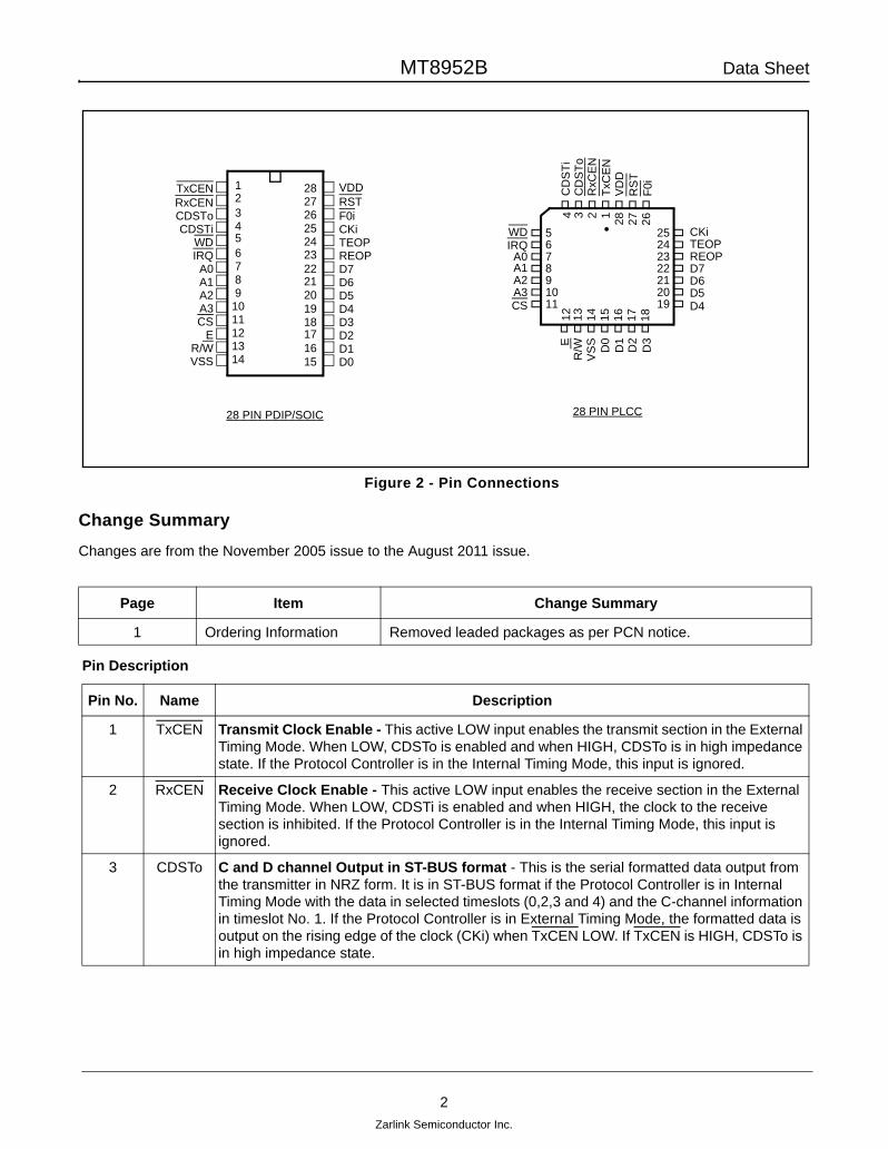
Figure 2 - Pin Connections
Change Summary
Changes are from the November 2005 issue to the August 2011 issue.
Page Item Change Summary
1 Ordering Information Removed leaded packages as per PCN notice.
Pin Description
Pin No. Name Description
1 TxCEN Transmit Clock Enable - This active LOW input enables the transmit section in the External Timing Mode. When LOW, CDSTo is enabled and when HIGH, CDSTo is in high impedance state. If the Protocol Controller is in the Internal Timing Mode, this input is ignored.
2 RxCEN Receive Clock Enable - This active LOW input enables the receive section in the External Timing Mode. When LOW, CDSTi is enabled and when HIGH, the clock to the receive section is inhibited. If the Protocol Controller is in the Internal Timing Mode, this input is ignored.
3 CDSTo C and D channel Output in ST-BUS format - This is the serial formatted data output from the transmitter in NRZ form. It is in ST-BUS format if the Protocol Controller is in Internal Timing Mode with the data in selected timeslots (0,2,3 and 4) and the C-channel information in timeslot No. 1. If the Protocol Controller is in External Timing Mode, the formatted data is output on the rising edge of the clock (CKi) when TxCEN LOW. If TxCEN is HIGH, CDSTo is in high impedance state.
28 PIN PLCC
TxCENRxCENCDSToCDSTi
WDIRQA0A1A2A3CS
ER/WVSS
VDDRSTF0iCKiTEOPREOPD7D6D5D4D3D2D1D0
28 PIN PDIP/SOIC
1234567891011121314 15
1617181920
2827262524232221
4
567891011
25242322212019
CD
ST
i
CKiTEOPREOPD7D6D5D4
WDIRQA0A1A2A3CS
D2
3 2 128 27
26
12
13
1 4 15
16
1 7 18
CD
ST
oR
xCE
NT
x CE
NV
DD
RS
TF
0i
ER
/WV
SS
D0
D1
D3
2
Zarlink Semiconductor Inc.

MT8952B Data Sheet
4 CDSTi C and D channel Input in ST-BUS format - This is the serial formatted data input to the receiver in NRZ form. It must be in ST-BUS format if the Protocol Controller is in Internal Timing Mode with the input data in selected timeslots (0,2,3 and 4) and the C-channel information in timeslot No.1. If the Controller is in External Timing Mode, the serial input data is sampled on the falling edge of the clock CKi when RxCEN is LOW. If RxCEN is HIGH, the clock to receive section is inhibited.
5 WD Watch-Dog Timer output - Normally a HIGH level output, going LOW if the Watchdog timer times out or if the external reset (RST) is held LOW. The WD output remains LOW as long as RST is held LOW.
6 IRQ Interrupt Request Output (Open Drain) - This active LOW output notifies the controlling microprocessor of an interrupt request. It goes LOW only when the bits in the Interrupt Enable Register are programmed to acknowledge the source of the interrupt as defined in the Interrupt Flag Register.
7-10 A0-A3 Address Bus Inputs - These bits address the various registers in the Protocol Controller. They select the internal registers in conjunction with CS, R/W inputs and E Clock. (Refer to Table 1.)
11 CS Chip Select Input - This is an active LOW input enabling the Read or Write operation to various registers in the Protocol Controller.
12 E Enable Clock Input - This input activates the Address Bus and R/W input and enables data transfers on the Data Bus.
13 R/W Read/Write Control - This input controls the direction of data flow on the data bus. When HIGH, the I/O buffer acts as an output driver and as an input buffer when LOW.
14 VSS Ground (0 Volt).
15-22 D0-D7 Bidirectional Data Bus - These Data Bus I/O ports allow the data transfer between the HDLC Protocol Controller and the microprocessor.
23 REOP Receive End Of Packet (Output) - This is a HIGH going pulse that occurs for one bit duration when a closing flag is detected on the incoming packets, or the incoming packet is aborted, or when an invalid packet of 24 or more bits is received.
24 TEOP Transmit End Of Packet (Output) - This is a HIGH going pulse that occurs for one bit duration when a packet is transmitted correctly or aborted.
25 CKi Clock Input (Bit rate clock or 2 x bit rate clock in ST-BUS format while in the Internal Timing Mode and bit rate Clock in the External Timing Mode) - This is the clock input used for shifting in/out the formatted packets. It can be at bit rate (C2i) or twice the bit rate (C4i) in ST-BUS format while the Protocol Controller is in the Internal Timing Mode. Whether the clock should be C2i (typically 2.048 MHz) or C4i (typically 4.096 MHz) is decided by the BRCK bit in the Timing Control Register. If the Protocol Controller is in the External Timing Mode, it is at the bit rate.
26 F0i Frame Pulse Input - This is the frame pulse input in ST-BUS format to establish the beginning of the frame in the Internal Timing Mode. This is also the signal clocking the watchdog timer.
27 RST RESET Input - This is an active LOW Schmitt Trigger input, resetting all the registers including the transmit and receive FIFOs and the watchdog timer.
28 VDD Supply (5 Volts).
Pin Description (continued)
Pin No. Name Description
3
Zarlink Semiconductor Inc.

MT8952B Data Sheet
Table 1 - Register Addresses
Introduction
The MT8952B HDLC Protocol Controller handles bit oriented protocol structure and formats the data as per thepacket switching protocol defined in the X.25 (Level 2) recommendations of the CCITT. It transmits and receives thepacketed data (information or control) serially in a format shown in Figure 3, while providing the data transparencyby zero insertion and deletion. It generates and detects the flags, various link channel states and the abortsequence. Further, it provides a cyclic redundancy check on the data packets using the CCITT defined polynomial.In addition, it can generate and detect a Go Ahead sequence and recognize a single byte address in the receivedframe. There is also a provision to disable the protocol functions and provide transparent access to the serial busthrough the parallel port.
Frame Format
All frames start with an opening flag and end with a closing flag as shown in Figure 3. Between these two flags, aframe contains the data and the frame check sequence (FCS).
Figure 3 - Frame Format
Flag
The flag is a unique pattern of 8 bits (01111110) defining the frame boundary. The transmit section generates theflags and appends them automatically to the frame to be transmitted. The receive section searches the incomingpackets for flags on a bit-by-bit basis and establishes frame synchronization. The flags are used only to identify andsynchronize the received frame and are not transferred to the FIFO.
Address Bits Registers
A3 A2 A1 A0 Read Write
0 0 0 0 FIFO Status -
0 0 0 1 Receive Data Transmit Data
0 0 1 0 Control Control
0 0 1 1 Receive Address Receive Address
0 1 0 0 C-Channel Control (Transmit) C-Channel Control (Transmit)
0 1 0 1 Timing Control Timing Control
0 1 1 0 Interrupt Flag Watchdog Timer
0 1 1 1 Interrupt Enable Interrupt Enable
1 0 0 0 General Status -
1 0 0 1 C-Channel Status (Receive) -
FLAG DATA FIELD FCS FLAG
One Byte
n Bytes (n 2)
Two Bytes
One Byte
4
Zarlink Semiconductor Inc.
MT8952B Data Sheet
Data
The data field refers to the Address, Control and Information fields defined in the CCITT recommendations. A validframe should have a data field of at least 16 bits. The first byte in the data field is the address of the frame. If RxADbit in the Control Register is HIGH, the incoming packet is recognized only if the address byte matches the bytestored in the Receive Address Register or the address byte is the All-Call Address (all ONEs). The LSB of theReceive Address Register is set LOW permanently and the comparison is done only on upper seven bits of thereceived address byte. The address detection can be limited only to the upper six bits by setting HIGH both RA6/7and RxAD bits in the Control Register.
Frame Check Sequence (FCS)
The 16 bits following the data field are the frame check sequence bits. The generator polynomial is:
G(x)=x16+x12+x5+1
The transmitter calculates the FCS on all bits of the data field and transmits after the data field and before the endflag. The receiver performs a similar computation on all bits of the received data and FCS fields and the result iscompared with FOB8Hex. If it matches, the received data is assumed error free. The error status of the receivedpacket is indicated by D7 and D6 bits in the FIFO Status Register.
Zero Insertion and Deletion
The Protocol Controller, while sending either data from the FIFO or the 16 bits FCS, checks the transmission on abit-by-bit basis and inserts a ZERO after every sequence of five contiguous ONEs (including the last five bits ofFCS) to ensure that the flag sequence is not simulated. Similarly the receiver examines the incoming frame contentand discards any ZERO directly following the five contiguous ONEs.
Abort
The transmitter aborts a frame by sending eight consecutive ONEs. The FA bit in the Control Register along with awrite operation to the Transmit Data Register enables the transmission of abort sequence instead of the bytewritten to the register. On the receive side, the ABRT bit in the General Status Register is set whenever an abortsequence (7 or more continuous 1’s) is received. The abort sequence causes the receiver to abandon whatever itwas doing and start searching for a start flag. The FA bit in the Interrupt Status Register is set when an abortsequence is received following a start flag and at least four data bytes (minimum for a valid frame).
Interframe Time Fill and Link Channel States
When the HDLC Protocol Controller is not sending packets, the transmitter can be in any of three states mentionedbelow depending on the status of the IFTF0 and IFTF1 bits in the Control Register. These bits are also used todisable the protocol function to provide the transparent parallel access to the serial bus through the microprocessorport.
Idle State
The Idle state is defined as 15 or more contiguous ONEs. When the HDLC Protocol Controller is observing thiscondition on the receiving channel, the Idle bit in the General Status Register is set HIGH. On the transmit side, theProtocol Controller ends the Idle state when data is loaded into the transmit FIFO.
Interframe Time Fill State
The Protocol Controller transmits continuous flags (7EHex) in Interframe time fill state and ends this state when datais loaded into the transmit FIFO.
5
Zarlink Semiconductor Inc.
MT8952B Data Sheet
Go Ahead State
Go Ahead is defined by the 9 bit sequence 011111110 (7FHex followed by a ZERO), and hence contiguous 7F’sappear as Go Aheads. Once the transmitter is in ‘Go Ahead’ state, it will continue to remain so even after the datais loaded into the FIFO. This state can only be changed by setting the IFTF bits in the Control Register to somethingother than ‘GO Ahead’. The reception of this sequence is indicated by GA bit in the General Status Register and theProtocol Controller can generate an interrupt if enabled to do so by the GA bit in the Interrupt Enable Register.
Transparent Data Transfer State
The Protocol Controller, in this state, disables the protocol functions defined earlier and provides bi-directionalaccess to the serial bit streams through the parallel port. Like other states, the transparent data transfer can beselected in both timing modes.
Invalid Frames
Any frame shorter than 32 bits between the opening and closing flags (corresponding to 16 bits of data and 16 bitsFCS) is considered invalid. The Protocol Controller ignores the frame only if the frame length is less than 24 bitsbetween the flags. For frames of length 24 to 32 bits, it transfers the data field to FIFO and tags it as having badFCS in the FIFO Status Register.
Functional Description
The functional block diagram of the HDLC Protocol Controller is shown in Figure 1. It has two ports. The serial porttransmits and receives formatted data packets and the parallel port provides a microprocessor interface for accessto various registers in the Protocol Controller.
The serial port can be configured to operate in two modes depending on the IC bit in the Timing Control Register. Itcan transmit/receive the packets on selected timeslots in ST- BUS format or it can, using the enable signals(TxCEN and RxCEN), transmit/receive the packets at a bit rate equal to CKi clock input.
The microprocessor port allows parallel data transfers between the Protocol Controller and a 6800/6809 systembus. This interface consists of Data Bus (D0-D7), Address Bus (A0-A3), E Clock, Chip Select (CS) and R/W control.The micro-processor can read and write to the various registers in the Protocol Controller. The addresses of theseregisters are given in Table 2. The IRQ is an open drain, active LOW output indicating an interrupt request to CPU.Control and monitoring of many different interrupts that may originate from the protocol controller is implemented bythe Interrupt Flag Register (IFR) and the Interrupt Enable Register (IER). Specific events have been described thatset a bit HIGH in the Interrupt Flag Register. Such an event does not necessarily interrupt the CPU. To assert aninterrupt (pull IRQ output LOW) the bit in IER that coincides with the Interrupt Flag Register must be set HIGH. TheIRQ bit in the General Status Register is the complement of IRQ pin status. If an interrupt is asserted, this bit will beset HIGH otherwise it will be LOW.
TEOP and REOP Outputs
The HDLC Protocol Controller provides two separate signals TEOP & REOP indicating the end of packettransmitted and received respectively. TEOP is a HIGH going pulse for one bit duration asserted during the last bitof the closing flag or Abort sequence of the transmit packet. REOP is also a HIGH going pulse occurring for one bitperiod when a closing flag is received or an incoming packet is aborted or an invalid packet of 24 or more bits isdetected. However, REOP is not generated for invalid packets of length less than 24 bits. These ‘end of packet’signals are useful in multiplexing several data links on to a single HDLC Protocol Controller.
Timing Modes
There are two timing modes the Protocol Controller can be run in. These timing modes refer only to theconfiguration of the serial port and are not related to the microprocessor port.
6
Zarlink Semiconductor Inc.
MT8952B Data Sheet
Internal Timing Mode
The Internal Timing Mode is intended for an easy interface to various products using ST-BUS architecture,particularly Zarlink’s Digital Network Interface Circuit (DNIC - MT8972). The data/packets are shifted in/out seriallyin ST-BUS format using the timing signals F0i and C2i/C4i. In addition to framing the data, the Protocol Controllerreserves one channel (channel-1) on the ST-BUS for carrying control information (C-channel) and this timeslot cannot be used for the packetized data. While the Protocol Controller is in the Internal Timing Mode, the clock input CKican be either at the bit rate or at 2×bit rate depending on the BRCK bit in the Timing Control Register as shown inTable 2.
Table 2 - Output Bit Rate In Internal Timing Mode
The Protocol Controller uses the ST-BUS timing signals F0i and C2i/C4i, and enables the transmitter and receiversections in the appropriate timeslots as determined by TC0-TC3 bits in the Timing Control Register.
The TxCEN and RxCEN inputs are ignored in this mode.
C-Channel Interface
This is a separate control channel (C-channel) interface relevant only in the Internal Timing Mode. The data storedin the C-Channel Control Register is shifted out during the channel-1 timeslot of the outgoing ST-BUS (CDSTo) andthe C1EN bit in the Timing Control Register enables the transmission. The transmission of C-Channel isindependent of packet/data transmission. The data received on channel-1 of the incoming ST-BUS (CDSTi) isshifted into the C-Channel Status Register independently and it is updated continuously.
Both the C-channel registers are accessible by the accompanying CPU through the parallel port.
External Timing Mode
In the External Timing Mode, the transmit and receive sections are enabled independently by TxCEN and RxCENcontrol inputs and the formatted data packets are shifted in/out serially at a rate equal to the clock frequency onCKi. The output is transmitted on the rising edge and the receiver samples the input on the falling edge of the clock.The TxCEN and RxCEN controls are independent and asynchronous and have effect only after the current bit in thepacket is transmitted/received.
Although the protocol controller provides the packetized data on a limited number of channels on the ST-BUS whileoperating in the Internal Timing Mode, it can packetize the data on any or all the channels of the ST-BUS if it isoperated in the External Timing Mode with appropriate enable signals on TxCEN and RxCEN.
Transparent Data Transfer
By setting the IFTF bits in the Control Register appropriately, the protocol functions can be disabled. This providesa bidirectional access to the serial port through the microprocessor interface, with 19 byte deep FIFO in eachdirection. The transparent data transfer facility functions in bytewide format and is available in both timing modesexcept when the timing control bits are set for one bit/frame during the Internal Timing Mode.
The transmit data is shifted out serially on CDSTo and the operation being bytewide, only the least significant bits ofeach byte loaded are transmitted, if the timing control bits are set to select 2, 6 or 7 bits/frame. When the transmitFIFO is empty, the last byte or the portion the last byte, written to the FIFO is transmitted repeatedly. Similarly theserial data on CDSTi is shifted in and converted to bytewide format. In case the timeslot selected is 2, 6 or 7bits/frame, the reception involves only the most significant bits of each byte.
BRCK Bit CKi Input Output Data Rate
0 4.096 MHz/C4i 2.048 Mbps
1 2.048 MHz/C2i 2.048 Mbps
7
Zarlink Semiconductor Inc.

MT8952B Data Sheet
It should be noted that none of the protocol related status or interrupt bits are applicable in transparent data transferstate. However, the FIFO related status and interrupt bits are pertinent and carry the same meaning as they dowhile performing the protocol functions.
Watchdog Timer
This is a fixed eleven stage binary counter with F0i as the input and WD as the output from the last stage. Thiscounter can be reset either by the external input (RST) or by writing XXX0 1010 to the Watchdog Timer Register.The WD output is normally HIGH and if the Watchdog Timer Register is not written within 210 cycles of F0i inputafter it is reset, the WD output will go LOW for a period of 210 cycles of F0i. Even though the F0i input is notrequired for formatting data in the External Timing Mode, it is necessary for the operation of the watchdog timer.
Order of Bit Transmission/Reception
The Least Significant Bit (LSB) corresponding to D0 on the data bus is transmitted first on the serial output(CDSTo). On the receiving side, the first bit received on the serial input (CDSTi) is considered as the LSB andplaced on D0 of the data bus.
Registers
There are several registers in the HDLC Protocol Controller accessible to the associated micro-processor via thedata bus. The addresses of these registers are given in Table 1 and their functional details are given below.
FIFO Status Register (Read)
This register (Figure 4) indicates the status of transmit and receive FIFOs and the received byte as describedbelow.
Figure 4 - FIFO Status Register
Rx Byte Status: These two bits (D7 and D6) indicate the status of the received byte ready to be read from thereceive FIFO. The status is encoded as shown in Table 3.
Table 3 - Received Byte Status
Rx FIFO Status: These bits (D5 and D4) indicate the status of receive FIFO as given by Table 4. The Rx FIFOstatus bits are not updated immediately after an access of the Rx FIFO (a read from the microprocessor port, or awrite from the serial port), to avoid the existence of unrecoverable error conditions.
When in external timing mode, the MT8952B must receive two falling edges of the clock signal at the CKi inputbefore the Rx FIFO status bits will be updated. When in internal 2.048 MHz timing mode, the MT8952B mustreceive two falling edges of the C2i clock before the Rx FIFO status bits will be updated. When in internal
D7 D6 D5 D4 D3 D2 D1 D0
Rx ByteStatus
Rx FIFOStatus
Tx FIFOStatus
LOW LOW
Rx ByteStatus Bits StatusD7 D6
0 0 Packet Byte
0 1 First Byte
1 0 Last Byte (Good FCS)
1 1 Last Byte (Bad FCS)
8
Zarlink Semiconductor Inc.

MT8952B Data Sheet
4.096 MHz timing mode, the MT8952B must receive four falling edges of the C4i clock before the Rx FIFOstatus bit will be updated (see the section on Receive Operation - Normal Packets).
Table 4 - Receive FIFO Status
Tx FIFO Status: These two bits (D3 and D2) indicate the status of transmit FIFO as shown in Table 5.
Table 5 - Transmit FIFO Status
The Tx FIFO status bits are updated in the same manner as the Rx FIFO bits, except that in external timing mode,and in internal 2.048 Mbps timing mode, the Tx FIFO status bits are updated after two falling edges of the CKi or theC2i signal (see the section on Transmit Operation - Normal Packets).
Receive Data Register (Read)
Reading the Receive Data Register (Figure 5) puts the first byte from the receive FIFO on the data bus. The first bitof the data received on the serial input (CDSTi) is considered to be the LSB and is available on D0 of the data bus.
Figure 5 - Receive Data Register
Transmit Data Register (Write)
Writing to Transmit Data Register (Figure 6) puts the data present on the data bus into the transmit FIFO. The LSB(D0) is transmitted first.
Figure 6 - Transmit Data Register
Rx FIFOStatus Bits StatusD5 D4
0 0 Rx FIFO Empty
0 1 Less than or equal to 14 bytes
1 0 Rx FIFO Full
1 1 Greater than or equal to 15 bytes
Tx FIFOStatus Bits StatusD3 D2
0 0 Tx FIFO Full
0 1 Greater than or equal to 5 bytes
1 0 Tx FIFO Empty
1 1 Less than or equal to 4 bytes
D7 D6 D5 D4 D3 D2 D1 D0
RD7 RD6 RD5 RD4 RD3 RD2 RD1 RD0
D7 D6 D5 D4 D3 D2 D1 D0
TD7 TD6 TD5 TD4 TD3 TD2 TD1 TD0
9
Zarlink Semiconductor Inc.

MT8952B Data Sheet
Control Register (Read/Write)
The Control Register (Figure 7) is used for general purpose control of the HDLC Protocol Controller. The bitscontained in this register and their functions are described below.
Figure 7 - Control Register
TxEN -Transmit Enable: When set HIGH, this bit enables the transmitter and when LOW, disables it setting theserial output (CDSTo) to high impedance state. If the transmitter is disabled during the transmission of a packetusing this bit, the Protocol Controller will wait until the completion of the packet and closing flag is transmitted or thepacket is aborted before setting the output (CDSTo) to high impedance state. Thus TxEN bit controls thetransmission packet by packet unlike TxCEN input (pin 1) which controls it bit-by-bit. However, if the ProtocolController is in transparent data transfer state, the transmission will be stopped within two bit periods (maximum)and set the output to high impedance state.
RxEN - Receive Enable: This bit enables the receiver when set HIGH and disables it when LOW. If this bit goesLOW during the reception of the packet, the receiver can only be disabled after the current packet and its closingflag are received or an abort is detected. Thus RxEN bit controls the receiver section packet by packet unlikeRxCEN input (pin 2) which controls it bit-by-bit. However, if the Protocol Controller is in transparent data transferstate, the receiver will be disabled immediately.
RxAD - Receive Address Detect: This bit when set HIGH, enables the address detection for the received packets.This causes the receiver to recognize only those packets having a unique address as programmed in the ReceiveAddress Register or if the address byte is the All-Call address (all ONEs). The address comparison is done only onseven bits (compatible to the first byte of the address field defined in LAPD-CCITT) and an All-Call is defined as allONEs in upper seven bits of the received address field. If RxAD is LOW, the address detection is disabled andevery valid packet is recognized.
RA6/7 - Receive Address Six/Seven bits: This bit, when set HIGH, limits the address detection only to the uppersix bits of the received address byte (last 6 bits of received address field) and when LOW, allows the addresscomparison on seven bits. An "all call", in this case is defined as all ONEs in the upper six bits only. RA6/7 isignored if the address detection is disabled (RxAD=0).
IFTF0 and IFTF1 - Interframe Time Fill: Setting these bits according to the table below (Table 6) causes thetransmitter to be in one of the active or idle states or allows the Protocol Controller to be in the transparent datatransfer state.
Table 6 - Interframe Time Fill Bits
D7 D6 D5 D4 D3 D2 D1 D0
TxEN RxEN RxAD RA6/7 IFTF1 IFTF0 FA EOP
IFTF BitsResult
IFTF1 IFTF0
0 0 Idle State (All ONEs)
0 1 Interframe Time Fill state(Continuous Flags)
1 0 Transparent Data Transfer
1 1 Go Ahead state (Continuous7FHEX)
10
Zarlink Semiconductor Inc.

MT8952B Data Sheet
FA - Frame Abort: When set HIGH, this bit’tags’ the next byte written to the transmit FIFO and causes an abortsequence (eight ONEs) to be transmitted when it reaches the bottom of the FIFO. The abort sequence will betransmitted instead of the byte that was tagged. The FA bit is cleared to ZERO upon writing the data to the transmitFIFO. As a result, a ‘read’ of this register bit will not reflect the last data written to it.
EOP - End Of Packet: Writing a ONE to this bit ‘tags’ the next byte written to the transmit FIFO to indicate that it isthe last data byte of the packet. This bit is cleared to ZERO upon writing the data to the transmit FIFO. As a result,a read of this register bit will not indicate the last data written to it.
Receive Address Register (Read/Write)
Figure 8 - Receive Address Register
The data in this register (Figure 8) defines the unique address for the HDLC Protocol Controller. If addressrecognition is enabled using the RxAD and RA6/7 bits in the Control Register, an incoming packet is recognizedonly if its address byte (seven or six most significant bits) matches the corresponding bits in this register or if theaddress is an "all-call". The LSB of the Receiver Address Register is set LOW permanently and the addresscomparison is done only on remaining bits of the register.
C-Channel Control Register (Read/Write)
Figure 9 - C-Channel Control Register
The data written to this register (Figure 9) is transmitted on channel-1 slot of the outgoing ST-BUS (CDSTo), whenenabled by C1EN bit in the Timing Control Register. This feature can only be used when the HDLC ProtocolController is in the Internal Timing Mode.
Timing Control Register (Read/Write)
The Timing Control Register (Figure 10) controls the timing mode and other related operations and provides asoftware reset to the Protocol Controller. The various bits in this register are described below:
Figure 10 - Timing Control Register
RST - Reset: When this bit is set HIGH, all the registers in the HDLC Protocol Controller are reset and the data inthe FIFOs is lost. This is equivalent to the external reset with the exception that the RST bit does not affect itself orthe Watchdog Timer Register and WD output. The RST bit must be “cleared” (written as a logic “0”) twice before theMT8952B will be removed from its reset state (see section on RESET operation).
IC - Internal Control: When this bit is cleared to ZERO, the Protocol Controller is in the External Timing Mode.The transmit and receive sections are enabled by the inputs TxCEN and RxCEN respectively, and F0i is used onlyfor the watchdog timer operation. When this bit is a ONE, the Protocol Controller is in the Internal Timing Mode. Thetransmit and receive sections are enabled by the internally generated timings derived from the inputs CKi and F0i.The F0i input defines the beginning of a frame (Figure 24) and the transmitter and receiver sections are enabled inthe timeslots as determined by the bits TCO-TC3. The inputs TxCEN and RxCEN are ignored in this mode.
D7 D6 D5 D4 D3 D2 D1 D0
RA7 RA6 RA5 RA4 RA3 RA2 RA1 RA0
D7 D6 D5 D4 D3 D2 D1 D0
CT7 CT6 CT5 CT4 CT3 CT2 CT1 CT0
D7 D6 D5 D4 D3 D2 D1 D0
RST IC C1EN BRCK TC3 TC2 TC1 TC0
11
Zarlink Semiconductor Inc.

MT8952B Data Sheet
C1EN - Channel-1 Enable: When HIGH, it enables the transmission of C-channel information on channel-1 time-slot of the outgoing ST-BUS (CDSTo) and when LOW, puts CDSTo into high impedance state during that period.However, the C-channel information is received independently and the C-channel Status Register is updatedcontinuously. Note that C1EN has relevance only during the Internal Timing Mode.
BRCK- Bit Rate Clock: This bit is used during the Internal Timing Mode to select the clock rate and ignored if theProtocol Controller is in the External Timing Mode. It should be set HIGH if the input clock (CKi) is at the bit rate(C2i) and should be LOW for the clock input at 2 x bit rate (C4i). In both cases, the clock should be properlyphase related to F0i as shown in Figure 25.
TC0-TC3 - Timing Control Bits: In the Internal Timing Mode the transmitter and the receiver sections are enabledduring the times defined by the Timing Control Bits TC0-TC3 (Table 7). This applies only to the ST-BUS channels 0,2, 3 and 4 carrying the packets or transparent data (channel-1 pertains to C-channel information). The outputCDSTo is put during the remaining time intervals not enabled by these bits.
X : Don’t Care Table 7 - Timing Control Bits
Interrupt Flag Register (Read)
Reading the Interrupt Flag Register puts the interrupt status bits on the data bus. This register is reset when it isread and a particular bit will not be set until its particular condition occurs again. The functional details of each bitare provided in Figure 11.
Figure 11 - Interrupt Flag Register
GA - Go Ahead: This bit when set HIGH, indicates the detection of ‘go ahead’ sequence on the incoming datastream (CDSTi).
EOPD - End of Packet Detect: A HIGH on this bit confirms the reception of an ‘end of packet’ flag, an abortsequence or an invalid packet of 24 or more bits on the incoming data stream (CDSTi).
Tx DONE - Transmitter Done: This bit, when HIGH, indicates that the packet transmission is complete and theTransmit FIFO is empty. The falling edge of TEOP output causes this interrupt status bit to be set HIGH if the FIFOis empty.
FA - Frame Abort: This bit is set HIGH to indicate that a frame abort has been detected on the incoming datastream.
Timing Control Bits ST-BUS Channel Number
Bits/FrameTC3 TC2 TC1 TC0
X 0 0 0 0 1
X 0 0 1 0 2
0 0 1 0 0 6
1 0 1 0 0 7
X 0 1 1 2 8
X 1 0 0 3 8
X 1 0 1 4 8
X 1 1 0 2 and 3 16
X 1 1 1 2, 3 and 4 24
D7 D6 D5 D4 D3 D2 D1 D0GA EOPD Tx
DONEFA Tx
4/19FULL
TxURUN
Rx15/19FULL
RxOFLW
12
Zarlink Semiconductor Inc.
MT8952B Data Sheet
Tx 4/19 FULL - Transmit FIFO 4/19 full: This bit if set HIGH, indicates that the transmit FIFO has only 4 bytesremaining in it and another 15 bytes could be loaded. This bit has significance only when the transmit FIFO is beingdepleted and not when it is getting loaded.
Tx URUN - Transmit FIFO underrun: This bit when HIGH, identifies that the transmit FIFO is empty without theProtocol Controller being given the ‘end of packet’ indication. This indicates that the transmit FIFO has underrunand the Protocol Controller will transmit an abort sequence automatically. Tx DONE will be set 8 bit times after TxURUN is set.
Rx15/19 FULL - Receive FIFO 15/19 full: This bit when HIGH, confirms that the receive FIFO has 15 bytes in itand it can receive four more bytes.
Rx OFLW - Receive FIFO overflow: This bit when set HIGH, indicates that the receive FIFO is full and a ‘write’occurred indicating an overflow. The byte causing this and all the subsequent bytes written while the FIFO is in thisstate are lost. The receiver begins to search for a new start flag.
Watchdog Timer Register (Write)
The Watchdog Timer Register operates in conjunction with the Watchdog Timer and the WD output. Writing thecode of XXX0 1010 in the register resets the WD timer. If the register is not re-written within 210 cycles of F0i afterresetting the timer, the WD output goes LOW. This register serves the sole purpose of resetting the timer and hencerelevant only if it is written with the above data.
Interrupt Enable Register (Read/Write)
This register enables/disables the interrupts as specified in the Interrupt Flag Register (IFR). Setting HIGH theappropriate bits in this register (IER) enables the associated interrupt source. However, the masked bits in the IFRare still valid but they do not cause the IRQ output to go LOW. The description of the bits enabling the variousinterrupts is identical to those of the Interrupt Flag Register.
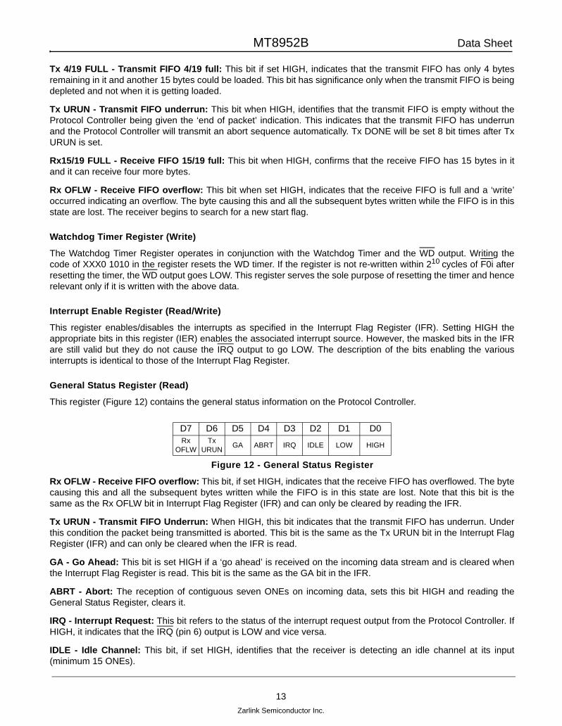
General Status Register (Read)
This register (Figure 12) contains the general status information on the Protocol Controller.
Figure 12 - General Status Register
Rx OFLW - Receive FIFO overflow: This bit, if set HIGH, indicates that the receive FIFO has overflowed. The bytecausing this and all the subsequent bytes written while the FIFO is in this state are lost. Note that this bit is thesame as the Rx OFLW bit in Interrupt Flag Register (IFR) and can only be cleared by reading the IFR.
Tx URUN - Transmit FIFO Underrun: When HIGH, this bit indicates that the transmit FIFO has underrun. Underthis condition the packet being transmitted is aborted. This bit is the same as the Tx URUN bit in the Interrupt FlagRegister (IFR) and can only be cleared when the IFR is read.
GA - Go Ahead: This bit is set HIGH if a ‘go ahead’ is received on the incoming data stream and is cleared whenthe Interrupt Flag Register is read. This bit is the same as the GA bit in the IFR.
ABRT - Abort: The reception of contiguous seven ONEs on incoming data, sets this bit HIGH and reading theGeneral Status Register, clears it.
IRQ - Interrupt Request: This bit refers to the status of the interrupt request output from the Protocol Controller. IfHIGH, it indicates that the IRQ (pin 6) output is LOW and vice versa.
IDLE - Idle Channel: This bit, if set HIGH, identifies that the receiver is detecting an idle channel at its input(minimum 15 ONEs).
D7 D6 D5 D4 D3 D2 D1 D0Rx
OFLWTx
URUNGA ABRT IRQ IDLE LOW HIGH
13
Zarlink Semiconductor Inc.

MT8952B Data Sheet
C-Channel Status Register (Read)
Figure 13 - C-Channel Status Register
The C-Channel Register (Figure 13) continuously stores the data received during the channel-1 timeslot of theincoming ST-BUS (CDSTi) during the Internal Timing Mode of the Protocol Controller.
Reset
When the MT8952B is reset by a low going pulse on the RST pin or by setting (logic high) the RST bit in the TimingControl Register, the device is put into the following state:
a. All bits in the Timing Control Register are cleared (logic 0) by an external reset. An internal reset clears all bits except the RST bit.
b. All bits in the Interrupt Enable Register are cleared (logic 0).
c. All bits in the Control Register are cleared (logic 0).
d. All bits in the Interrupt Register are cleared (logic 0).
e. All bits in the General Status Register are cleared (logic 0) except for the two least significant bits.
f. Receive and Transmit Registers are cleared and the FIFO Status Register reflects their state accordingly.
g. The WD output is reset low by an external reset but is not affected by an internal reset.
h. The Transmitter and the Receiver are disabled.
Transmit Operation
After a reset, which the external circuitry should provide upon power up, the transmit section is disabled. Beforeenabling this section, the timing should be set up. On reset, the serial port is set to External Timing Mode. In casethis is not desired, the Timing Control Register should be written to with the appropriate data. Once in the correcttiming mode, the Transmit Enable (TxEN) bit in the Control Register can be set. Now that the transmitter is enabledit will be in the Idle channel state. If any other channel state or the transparent data transfer facility is required, theIFTF bits in the Control Register should be set accordingly.
Normal Packets
To start a packet, the data is written into the transmit FIFO starting with the address field. All the data must bewritten to the FIFO in a bytewide manner. When the data is detected in the transmit FIFO, the protocol controller willproceed in one of the following ways:
If the transmitter is in idle state, the present byte of eight ONEs being transmitted is completed and then followedby a start flag and subsequently the data in the transmit FIFO is transmitted.
If the transmitter is in the interframe time fill state, the flag presently being transmitted is finished and then anotherstart flag is transmitted before transmitting the data from the transmit FIFO.
If the transmitter is in go ahead state, it continues to be in that state even after the data is loaded into the FIFO. Onlywhen the IFTF bits are set to choose something other than go ahead will the data be transmitted.
If the transmitter is in transparent data transfer state, the protocol functions are disabled and the data in the transmitFIFO is transmitted on CDSTo.
D7 D6 D5 D4 D3 D2 D1 D0
CR7 CR6 CR5 CR4 CR3 CR2 CR1 CR0
14
Zarlink Semiconductor Inc.

MT8952B Data Sheet
To indicate that the particular byte is the last byte of the packet, the EOP bit in the Control Register must be setbefore the last byte is written into the transmit FIFO. The EOP bit is cleared automatically when the data byte iswritten to the FIFO. After the transmission of the last byte in the packet, the frame check sequence (16 bits) is sentfollowed by a closing flag. If there is any more data in the transmit FIFO, another flag is transmitted followed by thenew data. In case of no data in the FIFO, the transmitter assumes the selected link channel state. During thetransmission of either the data or the frame check sequence, the Protocol Controller checks the transmittedinformation on a bit by bit basis and inserts a ZERO after every sequence of five consecutive ONEs.
Transmit FIFO Full
When the Transmit FIFO is full, this state is indicated by the Transmit FIFO status bits in the FIFO Status Register.These bits do not change state for two bit periods after an access of the FIFO from either the serial port or themicroprocessor port. The bit period is determined by the CKi signal frequency. If the bus cycle of the controllingmicroprocessor is much shorter than the bit period, the Transmit FIFO status bits may not be updated in time for thenext microprocessor read of the FIFO Status Register.
To make sure that the microprocessor does not overwrite the Tx FIFO, if over four bytes of information have beenwritten to the Tx FIFO, the microprocessor should wait for a 4/19 FULL interrupt before writing to the Tx FIFO again.When a 4/19 FULL interrupt has been received, a maximum of 15 bytes should be written to the Tx FIFO, thentransfer of information to the Tx FIFO should stop and the 4/19 FULL interrupt should be waited for once more. TheFIFO may be allowed to empty if no more information is to be sent at the moment. This procedure should keepsoftware independent of the frequency of the CKi signal.
Transmit Underrun
A transmit underrun occurs when the last byte loaded into the transmit FIFO was not ‘flagged’ with the ‘end ofpacket’ (EOP) bit and there are no more bytes in the FIFO. In such a situation, the Protocol Controller transmits theabort sequence (eight ONEs) and moves to the selected link channel state.
Abort Transmission
If it is desired to abort the packet currently being loaded into the transmit FIFO, the next byte written to the FIFOshould be ‘flagged’ to cause this to happen. The FA bit of the Control Register must be set HIGH, before writing thenext byte into the FIFO. This bit is cleared automatically once the byte is written to the FIFO. When the ‘flagged’byte reaches the bottom of the FIFO, a frame abort sequence is sent instead of the byte and the transmitteroperation returns to normal.
Go Ahead Transmission
By setting the IFTF bits in the Control Register appropriately the transmitter can be made to send the Go Aheadsequences when the Protocol Controller is not sending the packets. Since the go ahead is defined as 011111110,contiguous 7FHex’ s appear as go aheads. As long as the IFTF bits are set to choose go aheads, the transmitter willsend them even if data is subsequently loaded into the FIFO. Only when the IFTF bits are set to select somethingother than go aheads, will the data be transmitted.
C-Channel Transmission
By setting the C1EN bit in the Timing Control Register HIGH, the information loaded in the C-Channel ControlRegister can be transmitted over channel-1 timeslot of the outgoing ST-BUS (CDSTo). This is available only duringthe Internal Timing Mode of the Protocol Controller.
Transparent Data Transfer
The IFTF bits in the Control Register can be set to provide transparent data transfer disabling the protocolfunctions. The transmitter no longer generates the Flag, GA, Abort and Idle sequences nor does it insert the zerosand calculate the FCS. It operates in both timing modes in bytewide manner and transmits data serially on CDSTo.If the Protocol Controller is in the Internal Timing Mode and the Timing Control bits are set to select 2, 6 or 7
15
Zarlink Semiconductor Inc.

MT8952B Data Sheet
bits/frame, the corresponding least significant bits of every byte loaded into the transmit FIFO are only transmitted.The transparent data transfer facility is not available when the Timing Control bits are set for 1 bit/frame. In case theFIFO is empty, the last byte or the portion of the last byte, written to the FIFO is transmitted repeatedly. Note thatthe transparent data transfer can be disabled immediately in software (unlike during the transmission of packets)using TxEN bit in the Control Register.
The operation of the transmitter is similar in the External Timing Mode.
Receive Operation
After a reset on power up, the receive section is disabled. Timing set up considerations are similar to that of thetransmit section. Address detection is also disabled when a reset occurs. If address detection is required, theReceiver Address Register is loaded with the desired address and the RxAD bit in the Control Register is set HIGH.The receive section can then be enabled by RxEN bit in the Control Register.
Normal Packets
After initialization as explained above, the serial data starts to be clocked in and the receiver checks for the idlechannel and flags. If an idle channel is detected, the ‘Idle’ bit in the General Status Register is set HIGH. Once aflag is detected, the receiver synchronizes itself in a bytewide manner to the incoming data stream. The receiverkeeps resynchronizing to the flags until an incoming packet appears. The incoming packet is examined on a bit-by-bit basis, inserted zeros are deleted, the FCS is calculated and the data bytes are written into the receive FIFO.However, the FCS and other control characters like the flag, abort etc., never appear in the FIFO. If the addressdetection is enabled, the first byte following the flag is compared to the byte in the Receive Address Register and toAll-Call address. If a match is not found, the entire packet is ignored and nothing is written to the FIFO. If theincoming address byte is valid, the packet is received in normal fashion. All the bytes written to the receive FIFOare flagged with two status bits. The status bits are found in the FIFO status register and indicate whether the byteto be read from the FIFO is the first byte of the packet, the middle of the packet, the last byte of the packet withgood FCS or the last byte of the packet with bad FCS. This status indication is valid for the byte to be read from thereceive FIFO.
The incoming data is always written to the FIFO in a bytewide manner. However, in the event of data sent not beinga multiple of eight bits, the software associated with the receiver should be able to pick the data bits from the MSBpositions of the last byte in the received data written to the FIFO. The Protocol Controller does not provide anyindication as to how many bits this might be.
Receive FIFO Empty
When the Receive FIFO is empty, this state is indicated by the Receive FIFO status bits in the FIFO StatusRegister. As with the Tx FIFO status bits (see Transmit FIFO Full Section), these bits are not updated for two bitperiods after any access of the Receive FIFO. If the controlling microprocessor’s bus cycle is much shorter than abit period on the serial port, then the status bits may not be updated to indicate there is no information left in the RxFIFO before the microprocessor has returned to read the Rx FIFO again. The result is an underflow condition that isonly evident by redundant bytes in the received message.
To avoid a Rx FIFO underflow, reading information from the Rx FIFO should be approached in two ways. The firstapproach is to be used when the MT8952B indicates (via interrupt) that the Rx FIFO is 15/19 FULL. The controllingmicroprocessor should then immediately read 14 bytes from the Rx FIFO. This will avoid emptying the FIFO. Thesecond approach is to be used when an End of Packet interrupt is signalled by the MT8952B. The controllingmicroprocessor should then empty the Rx FIFO until the Rx Byte Status bits in the FIFO Status Register indicatethat the byte about to be read is the last byte. These bits are “tag“ bits whose state was determined before the Endof Packet condition was indicated, therefore their state is valid.
16
Zarlink Semiconductor Inc.

MT8952B Data Sheet
Invalid Packets
If there are less than 24 data bits between the opening and closing flags, the packet is considered invalid and thedata never enters the receive FIFO. This is true even with data and the abort sequence, the total of which is lessthan 24 bits. The data packets that are at least 24 bits but less than 32 bits long are also invalid, but not ignored.They are clocked into the receive FIFO and tagged as having bad FCS.
Frame Abort
When a frame abort is received the appropriate bits in the Interrupt Flag and Status Registers are set. The last byteof the packet that was aborted is written to the FIFO with a status of ‘packet byte’ tagged to it. The CPU determineswhich packet in the FIFO was aborted, if there is more than one packet in the FIFO, by the absence of ‘last byte’status on any of the bytes.
Idle Channel
While receiving the idle channel, the idle bit in the general status register remains set.
Go Ahead
The occurrence of this sequence can be used to generate an interrupt as described earlier. The receive circuitry willnot recognize a frame abort followed by a flag as go ahead.
C-Channel Reception
The information contained in channel-1 of the incoming ST-BUS (CDSTi) is shifted into the C-Channel StatusRegister during the Internal Timing Mode.
Transparent Data Transfer
By setting the IFTF bits in the Control Register to select the transparent data transfer, the receive section can bemade to disable the protocol functions like Flag/Abort/GA/Idle detection, zero deletion, CRC calculation andaddress comparison. The received data is shifted in from CDSTi and written to receive FIFO in bytewide format. Ifthe Protocol Controller is in the Internal Timing Mode and the Timing Control bits are set to 2, 6 or 7 bits/frame, therespective MSBs of each byte are only to be read from the data bus. The transparent data transfer facility is notavailable when the Timing Control bits are set to one bit/frame. The receive section can be disabled in softwareimmediately using the RxEN bit in the Control Register.
The operation of the receiver is similar in the External Timing Mode.
Receive Overflow
Receive overflow occurs when the receive section attempts to load a byte to an already full receive FIFO. Thisstatus can be used to generate the interrupt as described earlier.
Typical Connection
A typical connection to the HDLC Protocol Controller is shown in Figure 14. The parallel port interfaces with6800/6809 type processors. The bits A0-A3 are the addresses of various registers in the Protocol Controller. Themicroprocessor can read and write to these registers treating them as memory locations.
The serial port transmits/receives the packetized data. It can be connected to a digital transmission medium or to adigital network interface circuit. The TEOP and REOP are the ‘end of packet’ signals on transmit and receivedirection respectively. F0i and CKi are the timing signals with CKi accepting either the bit rate clock or 2 x bit rateclock in the internal timing mode. TxCEN and RxCEN are the enable inputs in the External Timing Mode.
17
Zarlink Semiconductor Inc.
MT8952B Data Sheet
WD is the output of the watchdog timer. It goes LOW when the timer times out or if the RST input is held LOW. Thisoutput can be used to reset the associated microprocessor. The RST is an active LOW input which resets theentire circuitry.
Figure 14 - Typical Connection Diagram
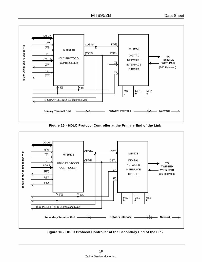
Applications
The MT8952B has a number of applications for transferring data or control information over a digital channel whileproviding built-in error detection capability. In combination with the MT8972 (the Digital Network Interface Circuit), itcan be used to transmit digital data over a twisted wire pair.
The block schematic of one such application is shown in Figures 15 and 16. They refer to the primary andsecondary ends of a voice/data communication link using the Digital Network Interface Circuits (DNIC). Each end isassociated with one DNIC which interfaces twisted wire pair to the digital data rate up to 160kbps (2B+D, framingsignal and housekeeping information).
PARALLEL
INTERFACING
WITH 6809
TYPE
PROCESSORS
SERIAL PORT
WITH
FORMATTED
DATA
D0-D7
R/W
CS
E
A0-A3
WD
IRQ
CDSTo
TEOP
TxCEN
CDSTi
REOP
RxCEN
MT8952B
HDLC Protocol
Controller
F0i CKi RST
VDD VSS
TIMING AND CONTROL
18
Zarlink Semiconductor Inc.
MT8952B Data Sheet
Figure 15 - HDLC Protocol Controller at the Primary End of the Link
Figure 16 - HDLC Protocol Controller at the Secondary End of the Link
MICROPROCESSOR
D0-D7
R/W
CS
E
A0-A3
WD
RST
IRQ
CDSTo
CDSTi
DSTi
DSTo
C4
F0
MS00
MS10
MS20
B-CHANNELS (2 X 64 kbits/sec Max)
MT8952B
HDLC PROTOCOL
CONTROLLER
MT8972
DIGITAL
NETWORK
INTERFACE
CIRCUIT
F0i CKi
TOTWISTED
WIRE PAIR
(160 kbits/sec)
Primary Terminal End Network Interface Network
MICROPROCESSOR
D0-D7
R/W
CS
E
A0-A3
WD
RST
IRQ
CDSTo
CDSTi
DSTi
DSTo
C4
F0
MS00
MS10
MS21
F0i CKi
B-CHANNELS (2 X 64 kbits/sec Max)
MT8952B
HDLC PROTOCOL
CONTROLLER
MT8972
DIGITAL
NETWORK
INTERFACE
CIRCUIT
TOTWISTED
WIRE PAIR
(160 kbits/sec)
Secondary Terminal End Network Interface Network
19
Zarlink Semiconductor Inc.

MT8952B Data Sheet
Primary End of the Link
The MT8952B is operating in the internal timing mode with the C-channel transceiver action enabled. Theprocessor loads the data or control information (D Channel) in the transmit FIFO which is packetized in HDLCformat and shifted out serially during the selected channels of the outgoing ST-BUS (CDSTo). The channels andthe number of bits per frame (frame period=125sec) can be selected by TC0-TC3 bits in the Timing ControlRegister. Since channel 1 is reserved for the C-channel information and channels 2 and 3 carry B-channels (64kbps each), the D-channel information can only be sent on channel-0. Similarly the incoming packets on CDSTi areloaded into receive FIFO after the removal of all overhead bits and checked for any errors. The microprocessor willthen read the data from the receive FIFO.
The DNIC (MT8972) is selected to operate in single port, master mode with the digital network (DN) option enabled.The B-channels, B1 and B2, are shown connected directly to the DNIC. Hence, these should be in ST-BUS formatenabled at the appropriate timeslot (channels 2 and 3). It can be the outputs of voice codecs (MT896X) providingvoice communication or data codecs (MT8950) for communication between RS232-C type terminals. It is possibleto use the HDLC protocol on B1 and B2 channels to provide the error detection.
This can be done by using a separate MT8952B enabled appropriately to shift out the formatted data duringchannels 2 and 3 or by multiplexing the same MT8952B between B- and D- channels.
Secondary End of the Link
At the secondary end of the communication link, a similar procedure is adopted to transmit/receive the data andcontrol information.
The MT8952B operates in the Internal Timing Mode as at the primary end, but the DNIC (MT8972) is selected tooperate in single port, slave mode with the digital network capability enabled.
The other functions and procedures are similar to those at the primary end.
The timing signals like CKi (C2i or C4i) and F0i are provided externally at the primary end and at the secondaryend, they are derived from the received data.
Although this application describes the communication between two stations over a dedicated link, it canbe modified to serve a switched communication path by additional control functions and a call set-up proceduremany of which can be achieved in software.
20
Zarlink Semiconductor Inc.

MT8952B Data Sheet
* Exceeding these values may cause permanent damage. Functional operation under these conditions is not implied.
‡ Typical figures are at 25C and are for design aid only: not guaranteed and not subject to production testing.
Absolute Maximum Ratings*
Parameter Symbol Min. Max. Units
1 Supply voltage VDD -0.3 7.0 V
2 Voltage on any pin (other than supply pins) VI VSS-0.3 VDD+0.3 V
3 Current on any pin (other than supply pins) II / IO 25 mA
4 DC Supply or ground current IDD / ISS 50 mA
5 Storage temperature TST -65 150 C
6 Package power dissipation Plastic PD 0.6 W
Recommended Operating Conditions - Voltages are with respect to ground (VSS) unless otherwise stated.
Characteristics Sym. Min. Typ.‡ Max. Units Test Conditions
1 Supply Voltage VDD 4.75 5.0 5.25 V
2 Input HIGH voltage VIH 2.4 VDD V For a Noise Margin of 400 mV
3 Input LOW voltage VIL VSS 0.4 V For a Noise Margin of 400 mV
4 Frequency of operation fCL 5.0 MHz When clock input is at twice the bit rate.
5 Operating temperature TA -40 25 85 C
DC Electrical Characteristics - Voltages are with respect to ground (VSS) unless otherwise stated.VDD=5V5%, VSS=0V, TA=-40 to 85C.
Characteristics Sym. Min. Typ.‡ Max. Units Test Conditions
1 Supply Current (Quiescent) IDD 1 10 A Outputs unloaded and clock input (CKi) grounded
2 Supply current (Operational) IDD 0.4 1.0 mA *See below
3
INPUT
Input HIGH voltage VIH 2.0 V
4 Input LOW voltage VIL 0.8 V
5 Input leakage current IIZ 10 A
6 Input capacitance Cin 10 pF
7 HIGH switching point for Schmitt Trigger (RST) input
VT+ 4.0 V
8 LOW switching point for Schmitt Trigger (RST) input
VT- 1.0 V
9 Hysteresis on Schmitt Trigger (RST) input
VH 0.5 V
21
Zarlink Semiconductor Inc.

MT8952B Data Sheet
‡ Typical figures are at 25C and are for design aid only: not guaranteed and not subject to production testing.* Outputs unloaded. Input pins 12 and 25 clocked at 2048 kHz. All other inputs at VSS.
† Timing is over recommended temperature & power supply voltages (VDD=5V5%, VSS=0V, TA=–40 to 85C).‡ Typical figures are at 25C and are for design aid only: not guaranteed and not subject to production testing.
10 OUTPUT
Output HIGH current (on all the outputs except IRQ)
IOH -5 -16 mA VOH=2.4 V
11 Output LOW current (on all the outputs including IRQ)
IOL 5 10 mA VOL=0.4 V
12 Output capacitance Co 15 pF
AC Electrical Characteristics† - Microprocessor Interface - (Figures 17 and 18)Voltages are with respect to ground (VSS) unless otherwise stated.
Characteristics Sym. Min. Typ.‡ Max. Units Test Conditions
1 Delay between CS and E clock tCSE 0 ns
2 Cycle time tCYC 205 ns
3 E Clock pulse width HIGH tEWH 145 ns
4 E Clock pulse width LOW tEWL 60 ns
5 Read/Write setup time tRWS 20 ns
6 Read/Write hold time tRWH 10 ns
7 Address setup time tAS 20 ns
8 Address hold time tAH 60 ns
9 Data setup time (write) tDSW 35 ns
10 Data hold time (write) tDHW 10 ns
11 E clock to valid data delay tDZLtDZH
145ns
Test load circuit 1 (Fig. 26) CL=200pF
12 Data hold time (read) tDLZtDHZ
10 60ns Test load circuit 3 (Fig. 26)
DC Electrical Characteristics - Voltages are with respect to ground (VSS) unless otherwise stated.VDD=5V5%, VSS=0V, TA=-40 to 85C.
Characteristics Sym. Min. Typ.‡ Max. Units Test Conditions
22
Zarlink Semiconductor Inc.
MT8952B Data Sheet
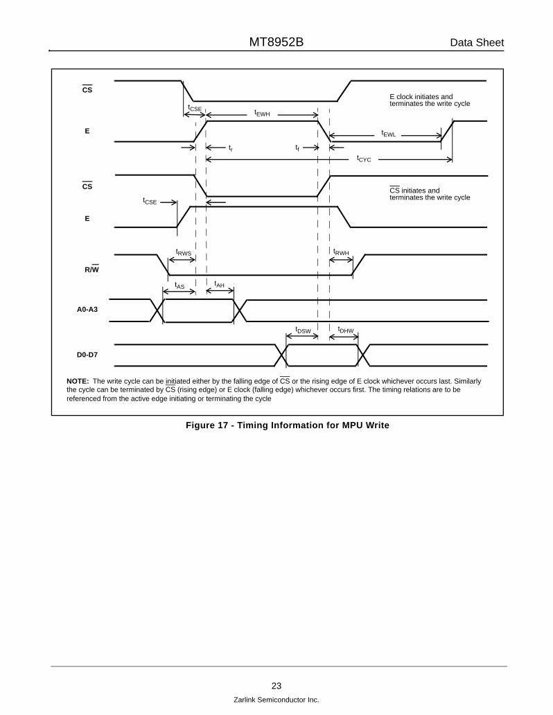
Figure 17 - Timing Information for MPU Write
CS
E
CS
E
R/W
A0-A3
D0-D7
NOTE: The write cycle can be initiated either by the falling edge of CS or the rising edge of E clock whichever occurs last. Similarlythe cycle can be terminated by CS (rising edge) or E clock (falling edge) whichever occurs first. The timing relations are to bereferenced from the active edge initiating or terminating the cycle
tCSE tEWH
tEWL
tr tftCYC
tCSE
tRWS tRWH
tAS tAH
tDSW tDHW
E clock initiates andterminates the write cycle
CS initiates andterminates the write cycle
23
Zarlink Semiconductor Inc.

MT8952B Data Sheet
Figure 18 - Timing Information for MPU Read
Figure 19 - Interrupt Request Release Time
CS
E
CS
E
R/W
A0-A3
D0-D7
E clock initiates andterminates the read cycle
CS initiates andterminates the read cycle
VALID DATAHigh Impedance High Impedance
tCSE tEWH
tr tftCYC
tCSE
tRWS tRWH
tAS tAH
tDZLtDZH
tDLZtDHZ
tEWL
NOTE: The read cycle can be initiated either by the falling edge of CS or the rising edge of E clock whichever occurs last. Similarlythe cycle can be terminated by CS (rising edge) or E clock (falling edge) whichever occurs first. The timing relations are to bereferenced from the active edge initiating or terminating the cycle.
E
IRQ
tIRQR
24
Zarlink Semiconductor Inc.
MT8952B Data Sheet
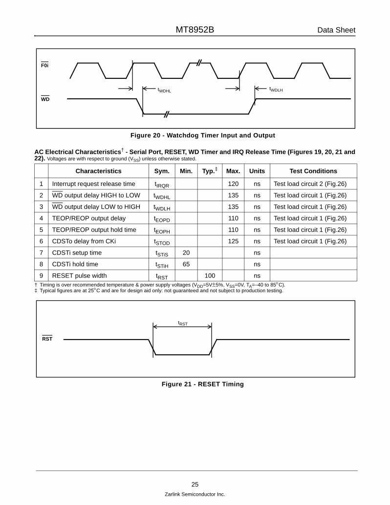
Figure 20 - Watchdog Timer Input and Output
† Timing is over recommended temperature & power supply voltages (VDD=5V5%, VSS=0V, TA=–40 to 85C).‡ Typical figures are at 25C and are for design aid only: not guaranteed and not subject to production testing.
Figure 21 - RESET Timing
AC Electrical Characteristics† - Serial Port, RESET, WD Timer and IRQ Release Time (Figures 19, 20, 21 and 22). Voltages are with respect to ground (VSS) unless otherwise stated.
Characteristics Sym. Min. Typ.‡ Max. Units Test Conditions
1 Interrupt request release time tIRQR 120 ns Test load circuit 2 (Fig.26)
2 WD output delay HIGH to LOW tWDHL 135 ns Test load circuit 1 (Fig.26)
3 WD output delay LOW to HIGH tWDLH 135 ns Test load circuit 1 (Fig.26)
4 TEOP/REOP output delay tEOPD 110 ns Test load circuit 1 (Fig.26)
5 TEOP/REOP output hold time tEOPH 110 ns Test load circuit 1 (Fig.26)
6 CDSTo delay from CKi tSTOD 125 ns Test load circuit 1 (Fig.26)
7 CDSTi setup time tSTiS 20 ns
8 CDSTi hold time tSTiH 65 ns
9 RESET pulse width tRST 100 ns
F0i
WD
tWDHL tWDLH
RST
tRST
25
Zarlink Semiconductor Inc.
MT8952B Data Sheet
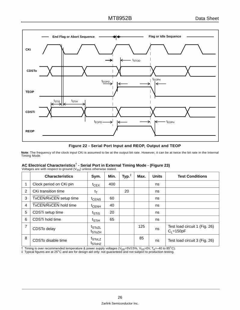
Figure 22 - Serial Port Input and REOP, Output and TEOP
Note: The frequency of the clock input CKi is assumed to be at the output bit rate. However, it can be at twice the bit rate in the Internal Timing Mode.
† Timing is over recommended temperature & power supply voltages (VDD=5V5%, VSS=0V, TA=–40 to 85C).‡ Typical figures are at 25C and are for design aid only: not guaranteed and not subject to production testing.
AC Electrical Characteristics† - Serial Port in External Timing Mode - (Figure 23)Voltages are with respect to ground (VSS) unless otherwise stated.
Characteristics Sym. Min. Typ.‡ Max. Units Test Conditions
1 Clock period on CKi pin tCEX 400 ns
2 CKi transition time tT 20 ns
3 TxCEN/RxCEN setup time tCENS 60 ns
4 TxCEN/RxCEN hold time tCENH 40 ns
5 CDSTi setup time tSTiS 20 ns
6 CDSTi hold time tSTiH 65 ns
7CDSTo delay
tSToZLtSToZH
125ns
Test load circuit 1 (Fig. 26) CL=150pF
8CDSTo disable time
tSToLZtSToHZ
85ns Test load circuit 3 (Fig. 26)
CKi
CDSTo
TEOP
CDSTi
REOP
End Flag or Abort Sequence Flag or Idle Sequence
tSTOD
tEOPDtEOPH
tSTiS tSTiH
tEOPD tEOPH
26
Zarlink Semiconductor Inc.
MT8952B Data Sheet
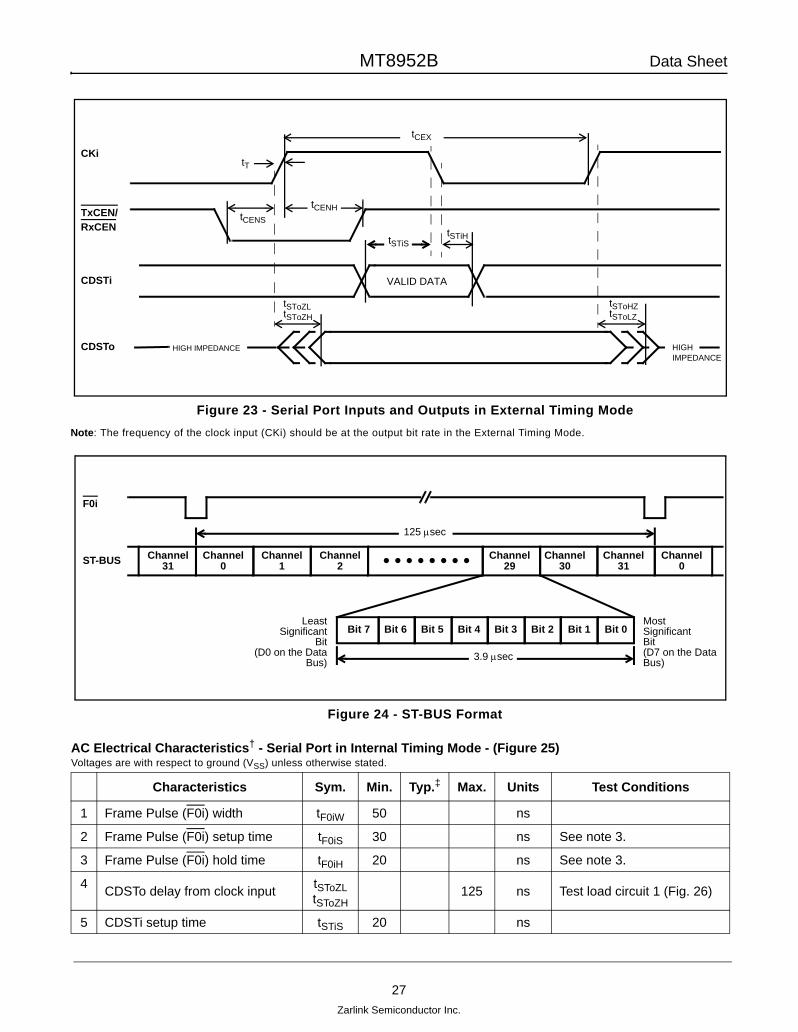
Figure 23 - Serial Port Inputs and Outputs in External Timing Mode
Note: The frequency of the clock input (CKi) should be at the output bit rate in the External Timing Mode.
Figure 24 - ST-BUS Format
AC Electrical Characteristics† - Serial Port in Internal Timing Mode - (Figure 25)Voltages are with respect to ground (VSS) unless otherwise stated.
Characteristics Sym. Min. Typ.‡ Max. Units Test Conditions
1 Frame Pulse (F0i) width tF0iW 50 ns
2 Frame Pulse (F0i) setup time tF0iS 30 ns See note 3.
3 Frame Pulse (F0i) hold time tF0iH 20 ns See note 3.
4CDSTo delay from clock input
tSToZLtSToZH
125 ns Test load circuit 1 (Fig. 26)
5 CDSTi setup time tSTiS 20 ns
CKi
TxCEN/RxCEN
CDSTi
CDSTo
VALID DATA
tCEX
tT
tCENS
tCENH
tSTiStSTiH
tSToZLtSToZH
tSToHZtSToLZ
HIGHIMPEDANCE
HIGH IMPEDANCE
Channel0
Channel1
Channel2 • • • • • • • •
Bit 7 Bit 6 Bit 5 Bit 4 Bit 3 Bit 2 Bit 1 Bit 0
125 sec
Channel31
Channel30
Channel31
Channel0
Channel29
F0i
ST-BUS
LeastSignificant
Bit
MostSignificantBit
3.9 sec(D0 on the DataBus)
(D7 on the DataBus)
27
Zarlink Semiconductor Inc.
MT8952B Data Sheet
† Timing is over recommended temperature & power supply voltages (VDD=5V5%, VSS=0V, TA=–40 to 85C).‡ Typical figures are at 25C and are for design aid only: not guaranteed and not subject to production testing.
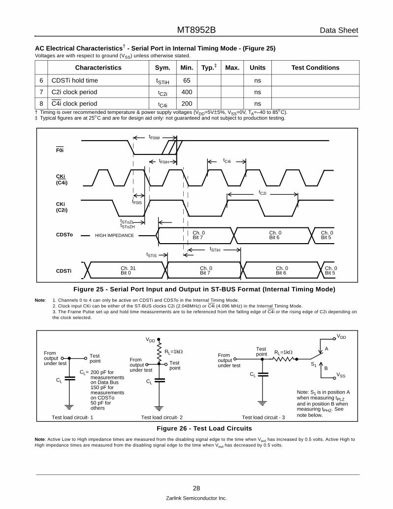
Figure 25 - Serial Port Input and Output in ST-BUS Format (Internal Timing Mode)
Note: 1. Channels 0 to 4 can only be active on CDSTi and CDSTo in the Internal Timing Mode.2. Clock input CKi can be either of the ST-BUS clocks C2i (2.048MHz) or C4i (4.096 MHz) in the Internal Timing Mode.3. The Frame Pulse set up and hold time measurements are to be referenced from the falling edge of C4i or the rising edge of C2i depending on the clock selected.
Figure 26 - Test Load Circuits
Note: Active Low to High impedance times are measured from the disabling signal edge to the time when Vout has increased by 0.5 volts. Active High to High impedance times are measured from the disabling signal edge to the time when Vout has decreased by 0.5 volts.
6 CDSTi hold time tSTiH 65 ns
7 C2i clock period tC2i 400 ns
8 C4i clock period tC4i 200 ns
AC Electrical Characteristics† - Serial Port in Internal Timing Mode - (Figure 25)Voltages are with respect to ground (VSS) unless otherwise stated.
Characteristics Sym. Min. Typ.‡ Max. Units Test Conditions
F0i
CKi(C4i)
CKi(C2i)
CDSTo
CDSTi
tF0iW
tF0iH tC4i
tF0iS
tC2i
tSToZLtSToZH
HIGH IMPEDANCE Ch. 0Bit 7
Ch. 0Bit 6
Ch. 0Bit 5
tSTiHtSTiS
Ch. 31Bit 0
Ch. 0Bit 7
Ch. 0Bit 6
Ch. 0Bit 5
Fromoutputunder test
Testpoint
CL
Test load circuit- 1
VDD
RL=1k
Testpoint
Fromoutputunder test
Test load circuit- 2 Test load circuit - 3
Fromoutputunder test
CL
CL
Testpoint
S1
VDD
VSS
RL=1k
Note: S1 is in position Awhen measuring tPLZand in position B whenmeasuring tPHZ. Seenote below.
CL= 200 pF for
on Data Bus150 pF formeasurementson CDSTo50 pF forothers
measurements
A
B
28
Zarlink Semiconductor Inc.

c Zarlink Semiconductor 2005. All rights reserved.
APPRD.
ISSUE
DATE
ACN
Package Code
Previous package codes

www.zarlink.com
Information relating to products and services furnished herein by Zarlink Semiconductor Inc. or its subsidiaries (collectively “Zarlink”) is believed to be reliable.However, Zarlink assumes no liability for errors that may appear in this publication, or for liability otherwise arising from the application or use of any suchinformation, product or service or for any infringement of patents or other intellectual property rights owned by third parties which may result from such application oruse. Neither the supply of such information or purchase of product or service conveys any license, either express or implied, under patents or other intellectualproperty rights owned by Zarlink or licensed from third parties by Zarlink, whatsoever. Purchasers of products are also hereby notified that the use of product incertain ways or in combination with Zarlink, or non-Zarlink furnished goods or services may infringe patents or other intellectual property rights owned by Zarlink.
This publication is issued to provide information only and (unless agreed by Zarlink in writing) may not be used, applied or reproduced for any purpose nor form partof any order or contract nor to be regarded as a representation relating to the products or services concerned. The products, their specifications, services and otherinformation appearing in this publication are subject to change by Zarlink without notice. No warranty or guarantee express or implied is made regarding thecapability, performance or suitability of any product or service. Information concerning possible methods of use is provided as a guide only and does not constituteany guarantee that such methods of use will be satisfactory in a specific piece of equipment. It is the user’s responsibility to fully determine the performance andsuitability of any equipment using such information and to ensure that any publication or data used is up to date and has not been superseded. Manufacturing doesnot necessarily include testing of all functions or parameters. These products are not suitable for use in any medical products whose failure to perform may result insignificant injury or death to the user. All products and materials are sold and services provided subject to Zarlink’s conditions of sale which are available on request.
Purchase of Zarlink’s I2C components conveys a license under the Philips I2C Patent rights to use these components in an I2C System, provided that the systemconforms to the I2C Standard Specification as defined by Philips.
Zarlink, ZL, the Zarlink Semiconductor logo and the Legerity logo and combinations thereof, VoiceEdge, VoicePort, SLAC, ISLIC, ISLAC and VoicePath aretrademarks of Zarlink Semiconductor Inc.
TECHNICAL DOCUMENTATION - NOT FOR RESALE
For more information about all Zarlink productsvisit our Web Site at