isl6531 datasheet - intersil · dual 5v synchronous buck pulse-width modulator (pwm) controller for...
TRANSCRIPT

FN9053Rev 2.00
Aug 11, 2005
ISL6531Dual 5V Synchronous Buck Pulse-Width Modulator (PWM) Controller for DDRAM Memory VDDQ and VTT Termination
DATASHEET
The ISL6531 provides complete control and protection for dual DC-DC converters optimized for high-performance DDRAM memory applications. It is designed to drive low cost N-channel MOSFETs in synchronous-rectified buck topology to efficiently generate 2.5V VDDQ for powering DDRAM memory, VREF for DDRAM differential signalling, and VTT for signal termination. The ISL6531 integrates all of the control, output adjustment, monitoring and protection functions into a single package.
The VDDQ output of the converter is maintained at 2.5V through an integrated precision voltage reference. The VREF output is precisely regulated to 1/2 the memory power supply, with a maximum tolerance of 1% over temperature and line voltage variations. VTT accurately tracks VREF. During V2_SD sleep mode, the VTT output is maintained by a low power window regulator.
The ISL6531 provides simple, single feedback loop, voltage-mode control with fast transient response for the VDDQ regulator. The VTT regulator features internal compensation that eases the design. It includes two phase-locked 300kHz triangle-wave oscillators which are displaced 90o to minimize interference between the two PWM regulators. The regulators feature error amplifiers with a 15MHz gain-bandwidth product and 6V/s slew rate which enables high converter bandwidth for fast transient performance. The resulting PWM duty ratio ranges from 0% to 100%.
The ISL6531 protects against overcurrent conditions by inhibiting PWM operation. The ISL6531 monitors the current in the VDDQ regulator by using the rDS(ON) of the upper MOSFET which eliminates the need for a current sensing resistor.
Ordering Information
Features
• Provides VDDQ, VREF, and VTT voltages for one- and two- channel DDRAM memory systems
• Excellent voltage regulation- VDDQ = 2.5V 2% over full operating range
- VREF = 1% over full operating range
- VTT = VREF 30mV
• Supports ‘S3’ sleep mode
- VTT is held at via a low power window regulator to minimize wake-up time
• Fast transient response
- Full 0% to 100% duty ratio
• Operates from +5V Input
• VTT regulator internally compensated
• Overcurrent fault monitor on VDD
- Does not require extra current sensing element- Uses MOSFET’s rDS(ON)
• Drives inexpensive N-Channel MOSFETs
• Small converter size
- 300kHz fixed frequency oscillator
• 24 Lead, SOIC or 32 Lead, 5mm5mm QFN
• Pb-Free Plus Anneal Available (RoHS Compliant)
Applications
• VDDQ, VTT, and VREF regulation for DDRAM memory systems- Main memory in AMD® Athlon™ and K8™, Pentium®
III, Pentium IV, Transmeta, PowerPC™, AlphaPC™, and UltraSparc® based computer systems
• High-power tracking DC-DC regulatorsPART NUMBER
TEMP RANGE(oC) PACKAGE PKG. DWG. #
ISL6531CB 0 to 70 24 Lead SOIC M24.3
ISL6531CBZ(See Note)
0 to 70 24 Lead SOIC(Pb-free)
M24.3
ISL6531CR 0 to 70 32 Lead 5x5 QFN L32.5x5
ISL6530/31EVAL1 Evaluation Board
Add “-T” suffix for tape and reel.NOTE: Intersil Pb-free plus anneal products employ special Pb-free material sets; molding compounds/die attach materials and 100% matte tin plate termination finish, which are RoHS compliant and compatible with both SnPb and Pb-free soldering operations. Intersil Pb-free products are MSL classified at Pb-free peak reflow temperatures that meet or exceed the Pb-free requirements of IPC/JEDEC J STD-020.
12--- VDDQ
12--- VDDQ
FN9053 Rev 2.00 Page 1 of 18Aug 11, 2005
ISL6531
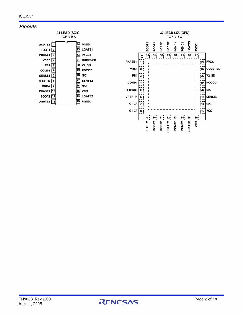
Pinouts24 LEAD (SOIC)
TOP VIEW32 LEAD 5X5 (QFN)
TOP VIEW
15
16
17
10
9
8VREF_IN
PHASE2
SENSE2
N/C
VCC
GNDA
18
19
20
21
22
23
24
7
6
5
4
3
2
1
BOOT1
PHASE1
FB1
SENSE1
VREF
PGND1
PVCC1
OCSET/SD
V2_SD
PGOOD
N/C
LGATE1
COMP1
UGATE1
13
14
12
11
UGATE2
LGATE2
PGND2
BOOT2
BO
OT
1
BO
OT
1
UG
AT
E1
UG
AT
E1
PG
ND
1
PG
ND
1
LG
AT
E1
PV
CC
1
PH
AS
E2
BO
OT
2
BO
OT
2
UG
AT
E2
PG
ND
2
PG
ND
2
LG
AT
E2
VC
C
PHASE 1
VREF
FB1
COMP1
SENSE1
VREF_IN
GNDA
GNDA
PVCC1
OCSET/SD
V2_SD
PGOOD
N/C
SENSE2
N/C
VCC
1
2
3
4
5
6
7
8
24
23
22
21
20
19
18
17
32 31 30 29 28 27 26 25
9 10 11 12 13 14 15 16
FN9053 Rev 2.00 Page 2 of 18Aug 11, 2005

ISL6531
Block Diagram
OSCILLATOR
SOFT-START
INHIBIT
PWMCOMPARATOR
ERRORAMP
VCC
PWM
PGND1
VREF
FB1
COMP1
OVER-CURRENT
GATECONTROL
LOGIC
BOOT1
UGATE1
PHASE1
40A+-
+- +
-
LGATE1
OCSET/SDPGOOD
+-
POWER-ONRESET (POR)
90o Phase
INHIBITPWM
COMPARATOR
ERRORAMP
PWM
GND
GATECONTROL
LOGIC
BOOT2
UGATE2
PHASE2
+-
+-
LGATE2
0.8VREFERENCE
V2_SD
WINDOWREGULATOR
PVCC1
VREF_IN
SENSE1
Shift
PGND2
VCC
SENSE2
+ -+ -+ -+ -0.
85X 1.
15X 0.
85X 1.
15X
Zf
Zc
FN9053 Rev 2.00 Page 3 of 18Aug 11, 2005

ISL6531
Typical Application
BOOT1
+5V
+5V
RESET
VREF(.5xVDDQ)
UGATE1
PHASE1
PVCC1
LGATE1
BOOT2
UGATE2
PHASE2
LGATE2
PGND2
PGND1
SENSE2SENSE1
FB1
COMP1
OCSET/SD
PGOODVCC
GNDA
V2_SD
VREF_IN
VREF
SLEEP
RFB1
COUT2
LOUT2
COUT1
LOUT1
Q1
Q2
Q3
Q4
DBOOT1
DBOOT2
CBOOT2
CBOOT1
ROCSET
PGOOD
ISL6531
VDDQ
VTT
FIGURE 1. TYPICAL APPLICATION FOR ISL6531
FN9053 Rev 2.00 Page 4 of 18Aug 11, 2005

ISL6531
Absolute Maximum Ratings Thermal InformationSupply Voltage, VCC . . . . . . . . . . . . . . . . . . . . . . . . . . . . . . . . +7.0VBoot Voltage, VBOOTn - VPHASEn. . . . . . . . . . . . . . . . . . . . . . +7.0VInput, Output or I/O Voltage. . . . . . . . . . . .GND -0.3V to VCC +0.3VESD Classification . . . . . . . . . . . . . . . . . . . . . . . . . . . . . . . . . Class 2
Operating ConditionsSupply Voltage, VCC . . . . . . . . . . . . . . . . . . . . . . . . . . . . +5V 10%Ambient Temperature Range. . . . . . . . . . . . . . . . . . . . . 0oC to 70oCJunction Temperature Range . . . . . . . . . . . . . . . . . . . 0oC to 125oC
Thermal Resistance JA (oC/W) JC (oC/W)
SOIC Package (Note 1) . . . . . . . . . . . . 65 N/AQFN Package (Note 2). . . . . . . . . . . . . 33 4
Maximum Junction Temperature . . . . . . . . . . . . . . . . . . . . . . 150oCMaximum Storage Temperature Range . . . . . . . . . -65oC to 150oCMaximum Lead Temperature (Soldering 10s) . . . . . . . . . . . . 300oC
(SOIC - Lead tips only)For Recommended soldering conditions see Tech Brief TB389.
CAUTION: Stresses above those listed in “Absolute Maximum Ratings” may cause permanent damage to the device. This is a stress only rating and operation of thedevice at these or any other conditions above those indicated in the operational sections of this specification is not implied.
NOTE:
1. JA is measured with the component mounted on a high effective thermal conductivity test board in free air. See Tech Brief TB379 for details.
2. JA is measured in free air with the component mounted on a high effective thermal conductivity test board with “direct attach” features. JC, the “case temp” is measured at the center of the exposed metal pad on the package underside. See Tech Brief TB379.
Electrical Specifications Recommended Operating Conditions with Vcc = 5V, unless otherwise noted.
PARAMETER SYMBOL TEST CONDITIONS MIN TYP MAX UNITS
VCC SUPPLY CURRENT
Nominal Supply ICC OCSET/SD=VCC; UGATE1, UGATE2, LGATE1, and LGATE2 Open
- 5 - mA
Shutdown Supply OCSET/SD=0V - 3 - mA
POWER-ON RESET
Rising VCC Threshold VOCSET/SD=4.5V 4.25 - 4.5 V
Falling VCC Threshold VOCSET/SD=4.5V 3.75 - 4.0 V
OSCILLATOR
Free Running Frequency VCC=5 275 300 325 kHz
REFERENCES
Reference Voltage(V2 Error Amp Reference)
VVREF SENSE1=2.5V 49.5 50.0 50.5 %SENSE1
V1 Error Amp Reference VoltageTolerance
- - 2 %
V1 Error Amp Reference VREF VCC=5 - 0.8 - V
ERROR AMPLIFIERS
DC Gain - 82 - dB
Gain-Bandwidth Product GBW - 15 - MHz
Slew Rate SR COMP=10pF - 6 - V/s
WINDOW REGULATOR
Load Current - ±10 - mA
Output Voltage Error V2_SD=VCC; ±10mA load on V2 - ±7 - %
GATE DRIVERS
Upper Gate Source (UGATE1 and 2) IUGATE VCC=5V, VUGATE=2.5V - -1 - A
Upper Gate Sink (UGATE1 and 2) IUGATE VUGATE-PHASE=2.5V - 1 - A
Lower Gate Source (LGATE1 and 2) ILGATE VCC=5V, VLGATE=2.5V - -1 - A
Lower Gate Sink (LGATE1 and 2) ILGATE VLGATE=2.5V - 2 - A
PROTECTION
OCSET/SD Current Source IOCSET VOCSET=4.5VDC 34 40 46 A
OCSET/SD Disable Voltage VRESET - 0.8 - V
FN9053 Rev 2.00 Page 5 of 18Aug 11, 2005

ISL6531
Functional Pin Description24 LEAD (SOIC)
TOP VIEW32 LEAD 5X5 (QFN)
TOP VIEW
BOOT1 and BOOT2These pins provide bias voltage to the upper MOSFET drivers. A single capacitor bootstrap circuit may be used to create a BOOT voltage suitable to drive a standard N-Channel MOSFET.
UGATE1 and UGATE2Connect UGATE1 and UGATE2 to the corresponding upper MOSFET gate. These pins provide the gate drive for the upper MOSFETs. UGATE2 is also monitored by the adaptive shoot through protection to determine when the upper FET of the VTT regulator has turned off.
LGATE1 and LGATE2Connect LGATE1 and LGATE2 to the corresponding lower MOSFET gate. These pins provide the gate drive for the lower MOSFETs. These pins are monitored by the adaptive shoot through protection circuitry to determine when the lower FET has turned off.
PGND1 and PGND2These are the power ground connections for the gate drivers of the PWM controllers. Tie these pins to the ground plane through the lowest impedence connection available.
OCSET/SDA resistor (ROCSET) connected from this pin to the drain of the upper MOSFET of the VDDQ regulator sets the overcurrent trip point. ROCSET, an internal 40A current source (IOCS), and the upper MOSFET on-resistance (rDS(ON)) set the VDDQ
converter overcurrent (OC) trip point according to the following equation:
An overcurrent trip cycles the soft-start function.
Pulling the OCSET/SD pin to ground resets the ISL6531 and all external MOSFETS are turned off allowing the two output voltage power rails to float.
PGOODA high level on this open-drain output indicates that both the VDDQ and VTT regulators are within normal operating voltage ranges.
GNDASignal ground for the IC. Tie this pin to the ground plane through the lowest impedence connection available.
VCCThe 5V bias supply for the chip is connected to this pin. This pin is also the positive supply for the lower gate driver, LGATE2. Connect a well decoupled 5V supply to this pin.
V2_SDA high level on the V2_SD input places the VTT controller into “sleep” mode. In sleep mode, both UGATE2 and LGATE2 are driven low, effectively floating the VTT supply.
15
16
17
10
9
8VREF_IN
PHASE2
SENSE2
N/C
VCC
GNDA
18
19
20
21
22
23
24
7
6
5
4
3
2
1
BOOT1
PHASE1
FB1
SENSE1
VREF
PGND1
PVCC1
OCSET/SD
V2_SD
PGOOD
N/C
LGATE1
COMP1
UGATE1
13
14
12
11
UGATE2
LGATE2
PGND2
BOOT2
BO
OT
1
BO
OT
1
UG
AT
E1
UG
AT
E1
PG
ND
1
PG
ND
1
LG
AT
E1
PV
CC
1
PH
AS
E2
BO
OT
2
BO
OT
2
UG
AT
E2
PG
ND
2
PG
ND
2
LG
AT
E2
VC
C
PHASE 1
VREF
FB1
COMP1
SENSE1
VREF_IN
GNDA
GNDA
PVCC1
OCSET/SD
V2_SD
PGOOD
N/C
SENSE2
N/C
VCC
1
2
3
4
5
6
7
8
24
23
22
21
20
19
18
17
32 31 30 29 28 27 26 25
9 10 11 12 13 14 15 16
IPEAK
IOCS ROCSET
rDS ON --------------------------------------------=
FN9053 Rev 2.00 Page 6 of 18Aug 11, 2005

ISL6531
While the VTT supply “floats”, it is held to about 50% of VDDQ via a low current window regulator which drives VTT via the SENSE2 pin. The window regulator can overcome up to at least 10mA of leakage on VTT.
While V2_SD is high, PGOOD is low.
PHASE1 and PHASE2Connect PHASE1 and PHASE2 to the corresponding upper MOSFET source. This pin is used as part of the upper MOSFET bootstrapped drives. PHASE1 is used to monitor the voltage drop across the upper MOSFET of the VDDQ regulator for overcurrent protection. The PHASE1 pin is monitored by the adaptive shoot through protection circuitry to determine when the upper FET of the VDDQ supply has turned off.
FB1, COMP1COMP1 and FB1 are the available external pins of the error amplifier for the VDDQ regulator. The FB1 pin is the inverting inputs of the error amplifier and the COMP1 pin is the associated output. An appropriate AC network across these pins is used to compensate the voltage-controlled feedback loop of the VDDQ converter.
VREF and VREF_INVREF produces a voltage equal to one half of the voltage on SENSE1. This low current output is connected to the VREF input of the DDRAM devices being powered. This same voltage is used as the reference input of the VTT error amplifier. Thus VTT is controlled to 50% of VDDQ.
VREF_IN is used as an option to overdrive the internal resistor divider network that sets the voltage for both VREF_OUT and the reference voltage for the VTT supply. A 100pF capacitor between VREF_IN and ground is recommended for proper operation.
PVCC1This is the positive supply for the lower gate driver, LGATE1. PVCC1 is connected to a well decoupled 5V.
SENSE1 and SENSE2Both SENSE1 and SENSE2 are connected directly to the regulated outputs of the VDDQ and VTT supplies, respectively. SENSE1 is used as an input to create the voltage at VREF_OUT and the reference voltage for the VTT supply. SENSE2 is used as the feedback pin of the VTT regulator and as the regulation point for the window regulator that is enabled in V2_SD mode.
Functional Description
OverviewThe ISL6531 contains control and drive circuitry for two synchronous buck PWM voltage regulators. Both regulators utilize 5V bootstrapped output topology to allow use of low cost N-Channel MOSFETs. The regulators are driven by 300kHz
clocks. The clocks are phase locked and displaced 90o to minimize noise coupling between the controllers.
The first regulator includes a precision 0.8V reference and is intended to provide the proper VDDQ to a DDRAM memory system. The VDDQ controller implements overcurrent protection utilizing the rDS(ON) of the upper MOSFET. Following a fault condition, the VDDQ regulator is softstarted via a digital soft-start circuit.
Included in the ISL6531 is a precision VREF reference output. VREF is a buffered representation of . VREF is derived via a precision internal resistor divider connected to the SENSE1 terminal.
The second PWM regulator is designed to provide VTT termination for the DDRAM signal lines. The reference to the VTT regulator is VREF. Thus the VTT regulator provides a termination voltage equal to . The drain of the upper MOSFET of the VTT supply is connected to the regulated VDDQ voltage. The VTT controller is designed to enable both sinking and sourcing current on the VTT rail.
Two benefits result from the ISL6531 dual controller topology. First, as VREF is always , the VTT supply will track the VDDQ supply during soft-start cycles. Second, the overcurrent protection incorporated into the VDDQ supply will simultaneously protect the VTT supply.
InitializationThe ISL6531 automatically initializes upon application of input power. Special sequencing of the input supplies is not necessary. The Power-On Reset (POR) function continually monitors the input bias supply voltage at the VCC pin. The POR function initiates soft-start operation after the 5V bias supply voltage exceeds its POR threshold.
Soft-StartThe POR function initiates the digital soft start sequence. The PWM error amplifier reference input for the VDDQ regulator is clamped to a level proportional to the soft-start voltage. As the soft-start voltage slews up, the PWM comparator generates PHASE pulses of increasing width that charge the output capacitor(s). This method provides a rapid and controlled output voltage rise. The soft-start sequence typically takes about 7ms.
With the VTT regulator reference held at it will automatically track the ramp of the VDDQ softstart, thus enabling a soft-start for VTT.
Figure 2 shows the soft-start sequence for a typical application. At T0, the +5V VCC bias voltage starts to ramp. Once the voltage on VCC crosses the POR threshold at time T1, both outputs begin their soft-start sequence. The triangle waveforms from the PWM oscillators are compared to the rising error amplifier output voltage. As the error amplifier voltage increases, the pulse-widths on the UGATE pins increase to reach their steady-state duty cycle at time t2.
12--- VDDQ
12--- VDDQ
12--- VDDQ
12--- VDDQ
FN9053 Rev 2.00 Page 7 of 18Aug 11, 2005

ISL6531
Shoot-Through ProtectionA shoot-through condition occurs when both the upper MOSFET and lower MOSFET are turned on simultaneously, effectively shorting the input voltage to ground. To protect the regulators from a shoot-through condition, the ISL6531 incorporates specialized circuitry which insures that complementary MOSFETs are not ON simultaneously.
The adaptive shoot-through protection utilized by the VDDQ regulator looks at the lower gate drive pin, LGATE1, and the phase node, PHASE1, to determine whether a MOSFET is ON or OFF. If PHASE1 is below 0.8V, the upper gate is defined as being OFF. Similarly, if LGATE1 is below 0.8V, the lower MOSFET is defined as being OFF. This method of shoot-through protection allows the VDDQ regulator to source current only.
Due to the necessity of sinking current, the VTT regulator employs a modified protection scheme from that of the VDDQ regulator. If the voltage from UGATE2 or from LGATE2 to GND is less than 0.8V, then the respective MOSFET is defined as being OFF and the other MOSFET is turned ON.
Since the voltage of the lower MOSFET gates and the upper MOSFET gate of the VTT supply are being measured to determine the state of the MOSFET, the designer is encouraged to consider the repercussions of introducing external components between the gate drivers and their respective MOSFET gates before actually implementing such measures. Doing so may interfere with the shoot-through protection.
Power Down ModeDDRAM systems include a sleep state in which the VDDQ voltage to the memories is maintained, but signaling is suspended. During this mode the VTT termination voltage is no longer needed. The only load placed on the VTT bus is the leakage of the associated signal pins of the DDRAM and memory controller ICs.
When the V2_SD input of the ISL6531 is driven high, the VTT regulator is placed into a “sleep” state. In the sleep state the main VTT regulator is disabled, with both the upper and lower MOSFETs being turned off. The VTT bus is maintained at close to via a low current window regulator which drives VTT via the SENSE2 pin. Maintaining VTT at consumes negligible power and enables rapid wake-up from sleep mode without the need of softstarting the VTT regulator. During this power down mode, PGOOD is held LOW.
Output Voltage SelectionThe output voltage of the VDDQ regulator can be programmed to any level between VIN (i.e. +5V) and the internal reference, 0.8V. An external resistor divider is used to scale the output voltage relative to the reference voltage and feed it back to the inverting input of the error amplifier, see Figure 3.F However, since the value of R1 affects the values of the rest of the compensation components, it is advisable to keep its value less than 5k. R4 can be calculated based on the following equation:
If the output voltage desired is 0.8V, simply route VDDQ back to the FB pin through R1, but do not populate R4.
VTT Reference OverdriveThe ISL6531 allows the designer to bypass the internal 50% tracking of VDDQ that is used as the reference for VTT. The ISL6531 was designed to divide down the VDDQ voltage by 50% through two internal matched resistances. These resistances are typically 200k.
FIGURE 2. SOFT-START INTERVAL
0V
TIME
VCC (5V)(1V/DIV)
T1 T2T0
VDDQ (2.5V)
VTT (1.25V)
12--- VDDQ
12--- VDDQ
R4 R1 0.8VVOUT1 0.8V–--------------------------------------=
FIGURE 3. OUTPUT VOLTAGE SELECTION OF VDDQ
+
R1
COUT1
+5V
VDDQ
R4
LOUT1
ISL6531
C4Q1
FB1
UGATE1
VCC
BOOT1
COMP1
D1
R2C2
C1R3
C3
PHASE1
LGATE1Q2
FN9053 Rev 2.00 Page 8 of 18Aug 11, 2005

ISL6531
One method that may be employed to bypass the internal VTT reference generation is to supply an external reference directly to the VREF_IN pin. When doing this the SENSE1 pin must remain unconnected. Caution must be exercised when using this method as the VTT regulator does not employ a soft start of its own.
A second method would be to overdrive the internal resistors. Figure 3 shows how to implement this method. The external resistors used to overdrive the internal resistors should be less than 2k and have a tolerance of 1% or better. This method still supplies a buffer between the resistor network and any loading on the VREF pin. If there is no loading on the VREF pin, then no buffering is necessary and the reference voltage created by the resistor network can be tied directly to VREF.
Converter ShutdownPulling and holding the OCSET/SD pin below 0.8V will shutdown both regulators. During this state, PGOOD will be held LOW. Upon release of the OCSET/SD pin, the IC enters into a soft start cycle which brings both outputs back into regulation.
Voltage MonitoringThe ISL6531 offers a PGOOD signal that will communicate whether the regulation of both VDDQ and VTT are within ±15% of regulation, the V2_SD pin is held low and the bias voltage of the IC is above the POR level. If all the criteria above are true, the PGOOD pin will be at a high impedence level. When one or more of the criteria listed above are false, the PGOOD pin will be held low.
Overcurrent ProtectionThe overcurrent function protects the converter from a shorted output by using the upper MOSFET on-resistance, rDS(ON), of VDDQ to monitor the current. This method enhances the converter’s efficiency and reduces cost by eliminating a current sensing resistor.
The overcurrent function cycles the soft-start function in a hiccup mode to provide fault protection. A resistor (ROCSET) programs the overcurrent trip level (see Figure 1). An internal 40A
(typical) current sink develops a voltage across ROCSET that is referenced to VIN. When the voltage across the upper MOSFET of VDDQ (also referenced to VIN) exceeds the voltage across ROCSET , the overcurrent function initiates a soft-start sequence.
Figure 5 illustrates the protection feature responding to an overcurrent event on VDDQ. At time t0, an overcurrent condition is sensed across the upper MOSFET of the VDDQ regulator. As a result, both regulators are quickly shutdown and the internal soft-start function begins producing soft-start ramps. The delay interval seen by the output is equivalent to three soft-start cycles. The fourth internal soft-start cycle initiates a normal soft-start ramp of the output, at time t1. Both outputs are brought back into regulation by time t2, as long as the overcurrent event has cleared.
Had the cause of the overcurrent still been present after the delay interval, the overcurrent condition would be sensed and both regulators would be shut down again for another delay interval of three soft start cycles. The resulting hiccup mode style of protection would continue to repeat indefinitely.
The overcurrent function will trip at a peak inductor current (IPEAK) determined by:
where IOCSET is the internal OCSET current source (40A typical). The OC trip point varies mainly due to the MOSFET rDS(ON) variations. To avoid overcurrent tripping in the normal operating load range, find the ROCSET resistor from the equation above with:
FIGURE 4. VTT REFERENCE OVERDRIVE
VREF +-
VREF_IN
SENSE1
TO ERRORAMPLIFIER
ISL6531VDDQ
RA
RB
FIGURE 5. OVERCURRENT PROTECTION RESPONSE
0V
TIME
VDDQ (2.5V)
T1T0 T2
VTT (1.25V)
INTERNAL SOFT-START FUNCTION
DELAY INTERVAL
IPEAK
IOCSET x ROCSETrDS ON
-----------------------------------------------------=
FN9053 Rev 2.00 Page 9 of 18Aug 11, 2005

ISL6531
1. The maximum rDS(ON) at the highest junction temperature.
2. The minimum IOCSET from the specification table.
3. Determine IPEAK for ,
whereI is the output inductor ripple current.
For an equation for the ripple current see the section under component guidelines titled Output Inductor Selection.
A small ceramic capacitor should be placed in parallel with ROCSET to smooth the voltage across ROCSET in the presence of switching noise on the input voltage.
Current SinkingThe ISL6531 VTT regulator incorporates a MOSFET shoot-through protection method which allows the converter to sink current as well as source current. Care should be exercised when designing a converter with the ISL6531 when it is known that the converter may sink current.
When the converter is sinking current, it is behaving as a boost converter that is regulating its input voltage. This means that the converter is boosting current into the input rail of the regulator. If there is nowhere for this current to go, such as to other distributed loads on the rail or through a voltage limiting protection device, the capacitance on this rail will absorb the current. This situation will the allow voltage level of the input rail to increase. If the voltage level of the rail is boosted to a level that exceeds the maximum voltage rating of any components attached to the input rail, then those components may experience an irreversible failure or experience stress that may shorten their lifespan. Ensuring that there is a path for the current to flow other than the capacitance on the rail will prevent this failure mode.
To insure that the current does not boost up the input rail voltage of the VTT regulator, it is recommended that the input rail of the VTT regulator be the output of the VDDQ regulator. The current being sunk by the VTT regulator will be fed into the VDDQ rail and then drawn into the DDR SDRAM memory module and back into the VTT regulator. Figure 6 shows the recommended configuration and the resulting current loop.
Application Guidelines
Layout ConsiderationsLayout is very important in high frequency switching converter design. With power devices switching efficiently at 300kHz, the resulting current transitions from one device to another cause voltage spikes across the interconnecting impedances and parasitic circuit elements. These voltage spikes can degrade efficiency, radiate noise into the circuit, and lead to device over-voltage stress. Careful component layout and printed circuit board design minimizes the voltage spikes in the converters.
As an example, consider the turn-off transition of the PWM MOSFET. Prior to turn-off, the MOSFET is carrying the full load current. During turn-off, current stops flowing in the MOSFET and is picked up by the lower MOSFET. Any parasitic inductance in the switched current path generates a large voltage spike during the switching interval. Careful component selection, tight layout of the critical components, and short, wide traces minimizes the magnitude of voltage spikes.
There are two sets of critical components in a DC-DC converter using the ISL6531. The switching components are the most critical because they switch large amounts o energy, and therefore tend to generate large amounts of noise. Next are the small signal components which connect to sensitive nodes or supply critical bypass current and signal coupling.
A multi-layer printed circuit board is recommended. Figure 7 shows the connections of the critical components in the converter. Note that capacitors CIN and COUT could each represent numerous physical capacitors. Dedicate one solid layer, usually a middle layer of the PC board, for a ground plane and make all critical component ground connections with vias to this layer. Dedicate another solid layer as a power plane and break this plane into smaller islands of common voltage levels. Keep the metal runs from the PHASE terminals to the output inductor short. The power plane should support the input power and output power nodes. Use copper filled polygons on the top and bottom circuit layers for the phase nodes. Use the remaining printed circuit layers for small signal wiring. The wiring traces from the GATE pins to the MOSFET gates should be kept short and wide enough to easily handle the 1A of drive current.f
The switching components should be placed close to the ISL6531 first. Minimize the length of the connections between the input capacitors, CIN, and the power switches by placing them nearby. Position both the ceramic and bulk input capacitors as close to the upper MOSFET drain as possible. Position the output inductor and output capacitors between the upper MOSFET and lower diode and the load.
The critical small signal components include any bypass capacitors, feedback components, and compensation components. Position the bypass capacitor, CBP, close to the
IPEAK IOUT MAX I 2
----------+
FIGURE 6. VTT CURRENT SINKING LOOP
DDRSDRAM
+5V
RT
+-
VREF
UGATE1
LGATE1
PHASE1
UGATE2
LGATE2
PHASE2
ISL6531
VDDQ
VTT
FN9053 Rev 2.00 Page 10 of 18Aug 11, 2005

ISL6531
VCC pin with a via directly to the ground plane. Place the PWM converter compensation components close to the FB and COMP pins. The feedback resistors for both regulators should also be located as close as possible to the relevant FB pin with vias tied straight to the ground plane as required.
VDDQ Feedback CompensationThis section discusses the feedback compensation of the VDDQ regulator. Figure 8 highlights the voltage-mode control loop for a synchronous-rectified buck converter. The output voltage (VOUT) is regulated to the Reference voltage level. The error amplifier (error amp) output (VE/A) is compared with the oscillator (OSC) triangular wave to provide a pulse-width
modulated (PWM) wave with an amplitude of VIN at the PHASE node. The PWM wave is smoothed by the output filter (LO and CO).
The modulator transfer function is the small-signal transfer function of VOUT/VE/A. This function is dominated by a DC gain and the output filter (LO and CO), with a double pole break frequency at FLC and a zero at FESR. The DC gain of the modulator is simply the input voltage (VIN) divided by the peak-to-peak oscillator voltage VOSC.
Modulator Break Frequency Equations
The compensation network consists of the error amplifier (internal to the ISL6531) and the impedance networks ZIN and ZFB. The goal of the compensation network is to provide a closed loop transfer function with the highest 0dB crossing frequency (f0dB) and adequate phase margin. Phase margin is the difference between the closed loop phase at f0dB and 180 degrees. The equations below relate the compensation network’s poles, zeros and gain to the components (R1, R2, R3, C1, C2, and C3) in Figure 7. Use these guidelines for locating the poles and zeros of the compensation network:
1. Pick gain (R2/R1) for desired converter bandwidth.
2. Place first zero below filter’s double pole (~75% FLC).
3. Place second zero at filter’s double pole.
4. Place first pole at the ESR zero.
VDDQ
ISLAND ON POWER PLANE LAYER
ISLAND ON CIRCUIT PLANE LAYER
LOUT1
COUT1
CIN
+5V VIN
KEY
COMP1
ISL6531
UGATE1
R4
R2A
CBP
FB1
GND
VCC
FIGURE 7. PRINTED CIRCUIT BOARD POWER PLANESAND ISLANDS
R1A
BOOT1
C2A
VIA CONNECTION TO GROUND PLANE
LO
AD
Q1
CBOOT1
PHASE1
D1
R3AC3A
C1A
Q2LGATE1
PHASE1
VTTLOUT2
COUT2
UGATE2
LO
AD
Q3
CBOOT2
PHASE2
Q4LGATE2
PHASE2
+5V VIN
BOOT2
D2 VDDQ
SENSE1
PGND1
PGND2
SENSE2 FIGURE 8. VOLTAGE-MODE BUCK CONVERTERCOMPENSATION DESIGN
VOUT
REFERENCE
LO
CO
ESR
VIN
DVOSC
ERRORAMP
PWMDRIVER
(PARASITIC)ZFB
+-
REFERENCE
R1
R3R2 C3
C1
C2
COMP
VOUT
FB
ZFB
ISL6531
ZIN
COMPARATOR
DRIVER
DETAILED COMPENSATION COMPONENTS
PHASE
VE/A
+-
+- ZIN
OSC
FLC1
2 x LO x CO
------------------------------------------= FESR1
2 x ESR x CO-------------------------------------------=
FN9053 Rev 2.00 Page 11 of 18Aug 11, 2005

ISL6531
5. Place second pole at half the switching frequency.
6. Check gain against error amplifier’s open-loop gain.
7. Estimate phase margin - repeat if necessary.
Compensation Break Frequency Equations
Figure 9 shows an asymptotic plot of the DC-DC converter’s gain vs frequency. The actual Modulator Gain has a high gain peak due to the high Q factor of the output filter and is not shown in Figure 9. Using the above guidelines should give a Compensation Gain similar to the curve plotted. The open loop error amplifier gain bounds the compensation gain. Check the compensation gain at FP2 with the capabilities of the error amplifier. The Closed Loop Gain is constructed on the graph of Figure 9 by adding the Modulator Gain (in dB) to the Compensation Gain (in dB). This is equivalent to multiplying the modulator transfer function to the compensation transfer function and plotting the gain..
The compensation gain uses external impedance networks ZFB and ZIN to provide a stable, high bandwidth (BW) overall loop. A stable control loop has a gain crossing with -20dB/decade slope and a phase margin greater than 45 degrees. Include worst case component variations when determining phase margin
VTT Feedback CompensationTo ease design and reduce the number of small-signal components required, the VTT regulator is internally compensated. The only stability criteria that needs to be met relates the minimum value of the inductor to the equivalent
ESR of the output capacitor bank as shown in the following equation:
whereLOUT(MIN) = minimum output inductor value at full output current
ESROUT = equivalent ESR of the output capacitor bank
VIN = Input voltage of the converter
The design procedure for this output should follow the following steps:
1. Choose the number and type of output capacitors to meet the output transient requirements based on the dynamic loading characteristics of the output.
2. Determine the equivalent ESR of the output capacitor bank and calculate the minimum output inductor value.
3. Verify that the chosen inductor meets this minimum value criteria at full output load. It is recommended that the chosen inductor be no more than 30% saturated at full output load.
Component Selection Guidelines
Output Capacitor SelectionAn output capacitor is required to filter the output and supply the load transient current. The filtering requirements are a function of the switching frequency and the ripple current. The load transient requirements are a function of the slew rate (di/dt) and the magnitude of the transient load current. These requirements are generally met with a mix of capacitors and careful layout.
Modern digital ICs can produce high transient load slew rates. High frequency capacitors initially supply the transient and slow the current load rate seen by the bulk capacitors. The bulk filter capacitor values are generally determined by the ESR (effective series resistance) and voltage rating requirements rather than actual capacitance requirements.
High frequency decoupling capacitors should be placed as close to the power pins of the load as physically possible. Be careful not to add inductance in the circuit board wiring that could cancel the usefulness of these low inductance components. Consult with the manufacturer of the load on specific decoupling requirements.
Use only specialized low-ESR capacitors intended for switching-regulator applications for the bulk capacitors. The bulk capacitor’s ESR will determine the output ripple voltage and the initial voltage drop after a high slew-rate transient. An aluminum electrolytic capacitor’s ESR value is related to the case size with lower ESR available in larger case sizes. However, the equivalent series inductance (ESL) of these capacitors increases with case size and can reduce the usefulness of the
FZ21
2 x R1 R3+ x C3-------------------------------------------------------=
FP11
2 x R2 x C1 x C2C1 C2+----------------------
---------------------------------------------------------=
FP21
2 x R3 x C3------------------------------------=
FZ11
2 R2 C2----------------------------------=
FIGURE 9. ASYMPTOTIC BODE PLOT OF CONVERTER GAIN
100
80
60
40
20
0
-20
-40
-60
FP1FZ2
10M1M100K10K1K10010
OPEN LOOPERROR AMP GAIN
FZ1 FP2
FLC FESR
COMPENSATION
GA
IN (
dB
)
FREQUENCY (Hz)
GAIN
MODULATORGAIN LOOP GAIN
20VIN
VOSC----------------
log
20 R2R1-------- log
LOUT MIN 20 106– ESROUT VIN
FN9053 Rev 2.00 Page 12 of 18Aug 11, 2005

ISL6531
capacitor to high slew-rate transient loading. Unfortunately, ESL is not a specified parameter. Work with your capacitor supplier and measure the capacitor’s impedance with frequency to select a suitable component. In most cases, multiple electrolytic capacitors of small case size perform better than a single large case capacitor.
Output Inductor SelectionThe output inductor is selected to meet the output voltage ripple requirements and minimize the converter’s response time to the load transient. Additionally, the output inductor for the VTT regulator has to meet the minimum value criteria for loop stability as described in the VTT Feedback Compensation section. The inductor value determines the converter’s ripple current and the ripple voltage is a function of the ripple current. The ripple voltage and current are approximated by the following equations:
Increasing the value of inductance reduces the ripple current and voltage. However, the large inductance values reduce the converter’s response time to a load transient.
One of the parameters limiting the converter’s response to a load transient is the time required to change the inductor current. Given a sufficiently fast control loop design, the ISL6531 will provide either 0% or 100% duty cycle in response to a load transient. The response time is the time required to slew the inductor current from an initial current value to the transient current level. During this interval the difference between the inductor current and the transient current level must be supplied by the output capacitor. Minimizing the response time can minimize the output capacitance required.
The response time to a transient is different for the application of load and the removal of load. The following equations give the approximate response time interval for application and removal of a transient load:
where: ITRAN is the transient load current step, tRISE is the response time to the application of load, and tFALL is the response time to the removal of load. The worst case response time can be either at the application or removal of load. Be sure to check both of these equations at the minimum and maximum output levels for the worst case response time.
Input Capacitor SelectionUse a mix of input bypass capacitors to control the voltage overshoot across the MOSFETs. Use small ceramic capacitors for high frequency decoupling and bulk capacitors to supply the current needed each time Q1 turns on. Place the small ceramic
capacitors physically close to the MOSFETs and between the drain of Q1 and the source of Q2.
The important parameters for the bulk input capacitor are the voltage rating and the RMS current rating. For reliable operation, select the bulk capacitor with voltage and current ratings above the maximum input voltage and largest RMS current required by the circuit. The capacitor voltage rating should be at least 1.25 times greater than the maximum input voltage and a voltage rating of 1.5 times is a conservative guideline. The RMS current rating requirement for the input capacitor of a buck regulator is approximately 1/2 the DC load current.
The maximum RMS current required by the regulator may be closely approximated through the following equation:
For a through hole design, several electrolytic capacitors may be needed. For surface mount designs, solid tantalum capacitors can be used, but caution must be exercised with regard to the capacitor surge currentrating. These capacitors must be capable of handling the surge-current at power-up. Some capacitor series available from reputable manufacturers are surge current tested.
MOSFET Selection/ConsiderationsThe ISL6531 requires two N-Channel power MOSFETs for each PWM regulator. These should be selected based upon rDS(ON), gate supply requirements, and thermal management requirements.
In high-current applications, the MOSFET power dissipation, package selection and heatsink are the dominant design factors. The power dissipation includes two loss components; conduction loss and switching loss. The conduction losses are the largest component of power dissipation for both the upper and the lower MOSFETs. These losses are distributed between the two MOSFETs according to duty factor. The switching losses seen when sourcing current will be different from the switching losses seen when sinking current. The VDDQ regulator will only source current while the VTT regulator can sink and source. When sourcing current, the upper MOSFET realizes most of the switching losses. The lower switch realizes most of the switching losses when the converter is sinking current (see the equations below). These equations assume linear voltage-current transitions and do not adequately model power loss due the reverse-recovery of the upper and lower MOSFET’s body diode. The gate-charge losses are dissipated by the ISL6531 and don't heat the MOSFETs. However, large gate-charge increases the switching interval, tSW which increases the MOSFET switching losses.
Ensure that both MOSFETs are within their maximum junction temperature at high ambient temperature by calculating the temperature rise according to package thermal-resistance specifications. A separate heat sink may be necessary depending
I =VIN - VOUT
fs x L
VOUT
VINVOUT = I x ESRx
tRISE =L x ITRAN
VIN - VOUTtFALL =
L x ITRAN
VOUT
IRMSMAX
VOUTVIN
---------------- IOUTMAX
2 112------
VIN VOUT–
L fs--------------------------------
VOUTVIN
---------------- 2
+
=
FN9053 Rev 2.00 Page 13 of 18Aug 11, 2005

ISL6531
upon MOSFET power, package type, ambient temperature and air flow.
Given the reduced available gate bias voltage (5V), logic-level or sub-logic-level transistors should be used for both N-MOSFETs. Caution should be exercised when using devices with very low gate thresholds (VTH). The shoot-through protection circuitry may be circumvented by these MOSFETs. Very high dv/dt transitions on the phase node may cause the Miller capacitance to couple the lower gate with the phase node and cause an undesireable turn on of the lower MOSFET while the upper MOSFET is on.
Bootstrap Component SelectionExternal bootstrap components, a diode and capacitor, are required to provide sufficient gate enhancement to the upper MOSFET. The internal MOSFET gate driver is supplied by the external bootstrap circuitry as shown in Figure 10. The boot capacitor, CBOOT, develops a floating supply voltage referenced to the PHASE pin. This supply is refreshed each cycle, when DBOOT conducts, to a voltage of VCC less the boot diode drop, VD, plus the voltage rise across QLOWER.
Just after the PWM switching cycle begins and the charge transfer from the bootstrap capacitor to the gate capacitance is complete, the voltage on the bootstrap capacitor is at its lowest point during the switching cycle. The charge lost on the bootstrap capacitor will be equal to the charge transferred to the equivalent gate-source capacitance of the upper MOSFET as shown:
where QGATE is the maximum total gate charge of the upper MOSFET, CBOOT is the bootstrap capacitance, VBOOT1 is the bootstrap voltage immediately before turn-on, and VBOOT2 is the bootstrap voltage immediately after turn-on.
The bootstrap capacitor begins its refresh cycle when the gate drive begins to turn-off the upper MOSFET. A refresh cycle ends when the upper MOSFET is turned on again, which varies depending on the switching frequency and duty cycle.
The minimum bootstrap capacitance can be calculated by rearranging the previous equation and solving for CBOOT.
Typical gate charge values for MOSFETs considered in these types of applications range from 20 to 100nC. Since the voltage drop across QLOWER is negligible, VBOOT1 is simply VCC - VD. A schottky diode is recommended to minimize the voltage drop across the bootstrap capacitor during the on-time of the upper MOSFET. Initial calculations with VBOOT2 no less than 4V will quickly help narrow the bootstrap capacitor range.
For example, consider an upper MOSFET is chosen with a maximum gate charge, Qg, of 100nC. Limiting the voltage drop across the bootstrap capacitor to 1V results in a value of no less than 0.1F. The tolerance of the ceramic capacitor should also be considered when selecting the final bootstrap capacitance value.
A fast recovery diode is recommended when selecting a bootstrap diode to reduce the impact of reverse recovery charge loss. Otherwise, the recovery charge, QRR, would have to be added to the gate charge of the MOSFET and taken into consideration when calculating the minimum bootstrap capacitance.
PLOWER = Io2 x rDS(ON) x (1 - D)
Where: D is the duty cycle = VOUT / VIN,tSW is the combined switch ON and OFF time, and
fs is the switching frequency.
LOSSES WHILE SOURCING CURRENT
LOSSES WHILE SINKING CURRENT
PLOWER Io2
rDS ON 1 D– 12--- Io VIN tSW fs+=
PUPPER Io2
rDS ON D 12--- Io VIN tSW fs+=
PUPPER = Io2 x rDS(ON) x D
QGATE CBOOT VBOOT1 VBOOT2– =
ISL6531
GND
LGATEn
UGATEn
PHASEn
BOOTn
VIN
NOTE:
NOTE:VG-S VCC
CBOOT
DBOOT
QUPPER
QLOWER+-
FIGURE 10. UPPER GATE DRIVE BOOTSTRAP
VG-S VCC -VD
+VD-
VCC
CBOOT
QGATEVBOOT1 V–
BOOT2
-----------------------------------------------------
FN9053 Rev 2.00 Page 14 of 18Aug 11, 2005

ISL6531
ISL6531 DC-DC Converter Application CircuitFigure 11 shows an application circuit for a DDR SDRAM power supply, including VDDQ (+2.5V) and VTT (+1.25V). Detailed information on the circuit, including a complete Billof-Materials and circuit board description, can be found
inApplication Note AN9993-of-Materials and circuit board description, can be found in Application Note AN9993 Application Note AN9993-of-Materials and circuit board description, can be found in Application Note AN9993.
Component Selection Notes:
C4,5,7,8,9,10,18,19 - Each 150mF, Panasonic EEF-UE0J151RD1,2 - Each 30mA Schottky Diode, MA732
L1,2 - Each 1mH Inductor, Panasonic P/N ETQ-P6F1ROSFAQ1,2 - Each Fairchild MOSFET; ITF86130DK8Q3 - Fairchild MOSFET; ITF86110DK8
FIGURE 11. DDR SDRAM VOLTAGE REGULATOR
BOOT1
+5V
UGATE1
PHASE1
PVCC1
LGATE1
BOOT2
UGATE2
PHASE2
LGATE2
PGND2
PGND1
SENSE2SENSE1
FB1
COMP1
OCSET/SD
PGOOD
VCC
GNDA
V2_SD
VREF_IN
VREF
R19
C18,19
L2
C7,8,9,10
L1
Q1
Q2
Q3
D1
D2
C16
C6
R1
ISL6531
VDDQ
VTT
C1 C2
C4,5
C15
C17
C26
R26
C25
R25
C27
@5A
@10A
R20
C30
1000pF3.48k 0.1F
C31.0F 150F(x2)
0.1F
1H
150F(x4)
0.1F
1.0F
0.1F
1H
150F(x2)1.43k
15000pF
100pF
5600pF
6.34k
3.01k
100
100pF
FN9053 Rev 2.00 Page 15 of 18Aug 11, 2005

ISL6531
Intersil products are manufactured, assembled and tested utilizing ISO9001 quality systems as notedin the quality certifications found at www.intersil.com/en/support/qualandreliability.html
Intersil products are sold by description only. Intersil may modify the circuit design and/or specifications of products at any time without notice, provided that such modification does not, in Intersil's sole judgment, affect the form, fit or function of the product. Accordingly, the reader is cautioned to verify that datasheets are current before placing orders. Information furnished by Intersil is believed to be accurate and reliable. However, no responsibility is assumed by Intersil or its subsidiaries for its use; nor for any infringements of patents or other rights of third parties which may result from its use. No license is granted by implication or otherwise under any patent or patent rights of Intersil or its subsidiaries.
For information regarding Intersil Corporation and its products, see www.intersil.com
For additional products, see www.intersil.com/en/products.html
© Copyright Intersil Americas LLC 2002-2005. All Rights Reserved.All trademarks and registered trademarks are the property of their respective owners.
FN9053 Rev 2.00 Page 16 of 18Aug 11, 2005

ISL6531
FN9053 Rev 2.00 Page 17 of 18Aug 11, 2005
Small Outline Plastic Packages (SOIC)
NOTES:
1. Symbols are defined in the “MO Series Symbol List” in Section 2.2 of Publication Number 95.
2. Dimensioning and tolerancing per ANSI Y14.5M-1982.
3. Dimension “D” does not include mold flash, protrusions or gate burrs. Mold flash, protrusion and gate burrs shall not exceed 0.15mm(0.006 inch) per side.
4. Dimension “E” does not include interlead flash or protrusions. Inter-lead flash and protrusions shall not exceed 0.25mm (0.010 inch) perside.
5. The chamfer on the body is optional. If it is not present, a visual index feature must be located within the crosshatched area.
6. “L” is the length of terminal for soldering to a substrate.
7. “N” is the number of terminal positions.
8. Terminal numbers are shown for reference only.
9. The lead width “B”, as measured 0.36mm (0.014 inch) or greater above the seating plane, shall not exceed a maximum value of0.61mm (0.024 inch)
10. Controlling dimension: MILLIMETER. Converted inch dimensions are not necessarily exact.
INDEXAREA
E
D
N
1 2 3
-B-
0.25(0.010) C AM B S
e
-A-
L
B
M
-C-
A1
A
SEATING PLANE
0.10(0.004)
h x 45o
C
H
µ
0.25(0.010) BM M
M24.3 (JEDEC MS-013-AD ISSUE C)24 LEAD WIDE BODY SMALL OUTLINE PLASTIC PACKAGE
SYMBOL
INCHES MILLIMETERS
NOTESMIN MAX MIN MAX
A 0.0926 0.1043 2.35 2.65 -
A1 0.0040 0.0118 0.10 0.30 -
B 0.013 0.020 0.33 0.51 9
C 0.0091 0.0125 0.23 0.32 -
D 0.5985 0.6141 15.20 15.60 3
E 0.2914 0.2992 7.40 7.60 4
e 0.05 BSC 1.27 BSC -
H 0.394 0.419 10.00 10.65 -
h 0.010 0.029 0.25 0.75 5
L 0.016 0.050 0.40 1.27 6
N 24 24 7
0o 8o 0o 8o -
Rev. 0 12/93

ISL6531
FN9053 Rev 2.00 Page 18 of 18Aug 11, 2005
Quad Flat No-Lead Plastic Package (QFN)Micro Lead Frame Plastic Package (MLFP)
L32.5x532 LEAD QUAD FLAT NO-LEAD PLASTIC PACKAGE(COMPLIANT TO JEDEC MO-220VHHD-2 ISSUE C
SYMBOL
MILLIMETERS
NOTESMIN NOMINAL MAX
A 0.80 0.90 1.00 -
A1 - - 0.05 -
A2 - - 1.00 9
A3 0.20 REF 9
b 0.18 0.23 0.30 5,8
D 5.00 BSC -
D1 4.75 BSC 9
D2 2.95 3.10 3.25 7,8
E 5.00 BSC -
E1 4.75 BSC 9
E2 2.95 3.10 3.25 7,8
e 0.50 BSC -
k 0.25 - - -
L 0.30 0.40 0.50 8
L1 - - 0.15 10
N 32 2
Nd 8 3
Ne 8 8 3
P - - 0.60 9
- - 12 9
Rev. 1 10/02
NOTES:
1. Dimensioning and tolerancing conform to ASME Y14.5-1994.
2. N is the number of terminals.
3. Nd and Ne refer to the number of terminals on each D and E.
4. All dimensions are in millimeters. Angles are in degrees.
5. Dimension b applies to the metallized terminal and is measured between 0.15mm and 0.30mm from the terminal tip.
6. The configuration of the pin #1 identifier is optional, but must be located within the zone indicated. The pin #1 identifier may beeither a mold or mark feature.
7. Dimensions D2 and E2 are for the exposed pads which provide improved electrical and thermal performance.
8. Nominal dimensions are provided to assist with PCB Land Pattern Design efforts, see Intersil Technical Brief TB389.
9. Features and dimensions A2, A3, D1, E1, P & are present when Anvil singulation method is used and not present for sawsingulation.
10. Depending on the method of lead termination at the edge of the package, a maximum 0.15mm pull back (L1) maybe present. Lminus L1 to be equal to or greater than 0.3mm.