iramx16up60b series integrated power hybrid ic for … sheets/infineon pdfs... · integrated power...
TRANSCRIPT

www.irf.com 1
Features
IRAMX16UP60BSeries
16A, 600Vwith Internal Shunt Resistor
Integrated Power Hybrid IC forAppliance Motor Drive Applications.DescriptionInternational Rectifier's IRAMX16UP60B is a 16A, 600V Integrated Power Hybrid IC with Internal ShuntResistor for Appliance Motor Drives applications such as air conditioning systems and compressor drivers aswell as for light industrial application. IR's technology offers an extremely compact, high performance ACmotor-driver in a single isolated package to simplify design.This advanced HIC is a combination of IR's low VCE(on) Punch-Through IGBT technology and the industrybenchmark 3 phase high voltage, high speed driver in a fully isolated thermally enhanced package.A built-in temperature monitor and over-current protection, along with the short-circuit rated IGBTs andintegrated under-voltage lockout function, deliver high level of protection and fail-safe operation. Using aSingle in line package (SiP2) with full transfer mold structure minimizes PCB space and resolve isolationproblems to heatsink.
PD-96-957 RevD
• Internal Shunt Resistor• Integrated Gate Drivers and Bootstrap Diodes• Temperature Monitor• Low VCE(on) Non Punch Through IGBT Technology• Undervoltage lockout for all channels• Matched propagation delay for all channels• Schmitt-triggered input logic• Cross-conduction prevention logic• Lower di/dt gate driver for better noise immunity• Motor Power range 0.75~2.2kW / 85~253 Vac• Isolation 2000VRMS min• UL certification pending (UL number: E78996)
Absolute Maximum RatingsParameter Description Value Units
VCES / VRRM IGBT/Diode Blocking Voltage 600
V+ Positive Bus Input Voltage 450
IO @ TC=25°C RMS Phase Current (Note 1) 16
IO @ TC=100°C RMS Phase Current (Note 1) 8
IO Pulsed RMS Phase Current (Note 2) 30
FPWM PWM Carrier Frequency 20 kHz
PD Power dissipation per IGBT @ TC =25°C 31 W
VISO Isolation Voltage (1min) 2000 VRMS
TJ (IGBT & Diodes) Operating Junction temperature Range -40 to +150
TJ (Driver IC) Operating Junction temperature Range -40 to +150
T Mounting torque Range (M3 screw) 0.5 to 1.0 Nm
Note 1: Sinusoidal Modulation at V+=400V, TJ=150°C, FPWM=16kHz, Modulation Depth=0.8, PF=0.6, See Figure 3.Note 2: tP<100ms; TC=25°C; FPWM=16kHz. Limited by IBUS-ITRIP, see Table "Inverter Section Electrical Characteristics"
V
A
°C

IRAMX16UP60B
2 www.irf.com
Internal Electrical Schematic - IRAMX16UP60B
23 VS1
24 HO1
25 VB1
1 VCC
2 HIN1
3 HIN2
4 HIN3
5 LIN1LIN2
6LIN3
7F8
ITRIP9
EN10
RCIN11
VSS12
COM13
22VB2
21HO2
20VS2
19VB3
18HO3
17VS3
V- (12)
VB1 (7)U, VS1 (8)
VB2 (4)V, VS2 (5)
VB3 (1)W, VS3 (2)
VCC (14)
VSS (23)
Driver IC
LO1 16
LO3 14
LO2 15
ITRIP (22)
HIN1 (15)HIN2 (16)HIN3 (17)
LIN1 (18)
LIN2 (19)
LIN3 (20)
V (10)+
VTH (13)
FLT-EN(21)
THERMISTOR

IRAMX16UP60B
www.irf.com 3
Symbol Parameter Min Max Units
IBDFBootstrap Diode Peak Forward Current
--- 4.5 A
PBR PeakBootstrap Resistor Peak Power (Single Pulse)
--- 25.0 W
VS1,2,3High side floating supply offset voltage
VB1,2,3 - 25 VB1,2,3 +0.3 V
VB1,2,3 High side floating supply voltage -0.3 600 V
VCCLow Side and logic fixed supply voltage
-0.3 20 V
VIN, VEN, VITRIP Input voltage LIN, HIN, EN, ITrip -0.3Lower of
(VSS+15V) or VCC+0.3V
V
Absolute Maximum Ratings (Continued)All voltages are absolute referenced to COM/ITRIP.
Conditions
tP= 10ms,TJ = 150°C, TC=100°C
tP=100µs, TC =100°CESR / ERJ series
Inverter Section Electrical Characteristics @TJ= 25°CSymbol Parameter Min Typ Max Units
V(BR)CESCollector-to-Emitter Breakdown Voltage
600 --- --- V
∆V(BR)CES / ∆T Temperature Coeff. Of Breakdown Voltage
--- 0.3 --- V/°C
--- 1.55 1.85
--- 1.80 2.10
--- 5 80 VIN=5V, V+=600V
--- 165 --- VIN=5V, V+=600V, TJ=150°C
--- 2.0 2.4
--- 1.4 1.9 IC=8A, TJ=150°C
-- -- 1.25
--- --- 1.10
RBR Bootstrap Resistor Value --- 22 --- Ω
∆RBR/RBR Bootstrap Resistor Tolerance --- --- ±5 %
IBUS_TRIPCurrent Protection Threshold (positive going)
21 --- 28 A
Conditions
ICESZero Gate Voltage Collector Current
µA
VCE(ON)Collector-to-Emitter Saturation Voltage
V
VIN=5V, IC=1.0mA(25°C - 150°C)
VIN=5V, IC=250µA
V
VBDFMBootstrap Diode Forward Voltage Drop
V
VFM Diode Forward Voltage Drop
IC=8A, VCC=15V, TJ=150°C
IC=8A, VCC=15V
TJ=25°C
TJ=25°C
IC=8A
IF=1A
IF=1A, TJ=125°C
TJ=-40°C to 125°CSee Fig. 2
IRAMX16UP60B
4 www.irf.com
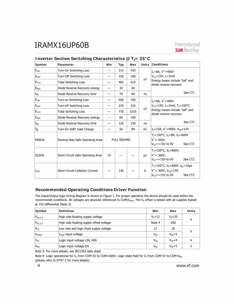
Inverter Section Switching Characteristics @ TJ= 25°CSymbol Parameter Min Typ Max Units
EON Turn-On Switching Loss --- 315 435
EOFF Turn-Off Switching Loss --- 150 180
ETOT Total Switching Loss --- 465 615
EREC Diode Reverse Recovery energy --- 30 60
tRR Diode Reverse Recovery time --- 70 90 ns
EON Turn-on Switching Loss --- 500 700
EOFF Turn-off Switching Loss --- 270 335
ETOT Total Switching Loss --- 770 1035
EREC Diode Reverse Recovery energy --- 60 100
tRR Diode Reverse Recovery time --- 120 150 ns
QG Turn-On IGBT Gate Charge --- 56 84 nC
RBSOA Reverse Bias Safe Operating Area
SCSOA Short Circuit Safe Operating Area 10 --- --- µs
ICSC Short Circuit Collector Current --- 140 --- A
µJ
µJ
IC=15A, V+=400V, VGE=15V
TJ=150°C, IC=8A, VP=600V
V+= 450VVCC=+15V to 0V See CT3
TJ=150°C, VP=600V,
V+= 360V,VCC=+15V to 0V See CT2
TJ=150°C, VP=600V, tSC<10µs
V+= 360V, VGE=15VVCC=+15V to 0V See CT2
FULL SQUARE
Conditions
IC=8A, V+=400VVCC=15V, L=2mHEnergy losses include "tail" and diode reverse recovery
See CT1
IC=8A, V+=400VVCC=15V, L=2mH, TJ=150°CEnergy losses include "tail" and diode reverse recovery
See CT1
Recommended Operating Conditions Driver Function
Symbol Definition Min Max Units
VB1,2,3 High side floating supply voltage VS+12 VS+20
VS1,2,3 High side floating supply offset voltage Note 4 450
VCC Low side and logic fixed supply voltage 12 20
VITRIP ITRIP input voltage VSS VSS+5
VIN Logic input voltage LIN, HIN VSS VSS+4 V
VEN Logic input voltage EN VSS VSS+5 V
Note 3: For more details, see IR21363 data sheet
The Input/Output logic timing diagram is shown in Figure 1. For proper operation the device should be used within therecommende conditions. All voltages are absolute referenced to COM/ITRIP. The VS offset is tested with all supplies biased at 15V differential (Note 3)
V
V
Note 4: Logic operational for Vs from COM-5V to COM+600V. Logic state held for Vs from COM-5V to COM-VBS. (please refer to DT97-3 for more details)

IRAMX16UP60B
www.irf.com 5
Static Electrical Characteristics Driver Function
Symbol Definition Min Typ Max Units
VINH , VENH Logic "0" input voltage 3.0 --- --- V
VINL , VENL Logic "1" input voltage --- --- 0.8 V
VCCUV+, VBSUV+ VCC and VBS supply undervoltage Positive going threshold 10.6 11.1 11.6 V
VCCUV-, VBSUV- VCC and VBS supply undervoltage Negative going threshold 10.4 10.9 11.4 V
VCCUVH, VBSUVH VCC and VBS supply undervoltage lock-out hysteresis --- 0.2 --- V
VIN,Clamp Input Clamp Voltage (HIN, LIN, ITRIP) IIN=10µA 4.9 5.2 5.5 V
IQBS Quiescent VBS supply current VIN=0V --- --- 165 µA
IQCC Quiescent VCC supply current VIN=0V --- --- 3.35 mA
ILK Offset Supply Leakage Current --- --- 60 µA
IIN+, IEN+ Input bias current VIN=5V --- 200 300 µA
IIN-, IEN- Input bias current VIN=0V --- 100 220 µA
ITRIP+ ITRIP bias current VITRIP=5V --- 30 100 µA
ITRIP- ITRIP bias current VITRIP=0V --- 0 1 µA
V(ITRIP) ITRIP threshold Voltage 440 490 540 mV
V(ITRIP, HYS) ITRIP Input Hysteresis --- 70 --- mV
RON,FLT Fault Output ON Resistance --- 50 100 ohm
VBIAS (VCC, VBS1,2,3)=15V, unless otherwise specified. The VIN and IIN parameters are referenced to COM/ITRIP and are applicable to all six channels. (Note 3)
Dynamic Electrical Characteristics
Symbol Parameter Min Typ Max Units Conditions
TONInput to Output propagation turn-on delay time (see fig.11)
--- 590 --- ns
TOFFInput to Output propagation turn-off delay time (see fig. 11)
--- 660 --- ns
TFLIN Input Filter time (HIN, LIN) 100 200 --- ns VIN=0 & VIN=5V
TBLT-Trip ITRIP Blancking Time 100 150 ns VIN=0 & VIN=5V
DT Dead Time (VBS=VDD=15V) 220 290 360 ns VBS=VCC=15V
MTMatching Propagation Delay Time (On & Off)
--- 40 75 nsVCC= VBS= 15V, external dead time> 400ns
TITripITrip to six switch to turn-off propagation delay (see fig. 2)
--- --- 1.75 µsVCC=VBS= 15V, IC=8A,
V+=400V
--- 7.7 --- TC = 25°C
--- 6.7 --- TC = 100°C
Post ITrip to six switch to turn-off clear time (see fig. 2)
TFLT-CLR ms
Driver only timing unless otherwise specified.
VCC=VBS= 15V, IC=8A,
V+=400V

IRAMX16UP60B
6 www.irf.com
Input-Output Logic Level Table
FLT- EN ITRIP HIN1,2,3 LIN1,2,3 U,V,W
1 0 0 1 V+
1 0 1 0 01 0 1 1 Off1 1 X X Off0 X X X Off
Ho
Lo
U,V,WIC
Driver
V+
Hin1,2,3
Lin1,2,3
(15,16,17)
(18,19,20)
(8,5,2)
Thermal and Mechanical CharacteristicsSymbol Parameter Min Typ Max Units Conditions
Rth(J-C) Thermal resistance, per IGBT --- 3.5 4.0
Rth(J-C) Thermal resistance, per Diode --- 5.0 5.5
Rth(C-S) Thermal resistance, C-S --- 0.1 ---
CD Creepage Distance 3.2 --- --- mm See outline Drawings
°C/WFlat, greased surface. Heatsink compound thermal conductivity 1W/mK
Internal NTC - Thermistor CharacteristicsParameter Definition Min Typ Max Units Conditions
R25 Resistance 97 100 103 kΩ TC = 25°C
R125 Resistance 2.25 2.52 2.80 kΩ TC = 125°C
B B-constant (25-50°C) 4165 4250 4335 k R2 = R1e [B(1/T2 - 1/T1)]
Temperature Range -40 125 °C
Typ. Dissipation constant 1 mW/°C TC = 25°C
Internal Current Sensing Resistor - Shunt CharacteristicsSymbol Parameter Min Typ Max Units Conditions
RShunt Resistance 17.9 18.1 18.3 mΩ TC = 25°C
TCoeff Temperature Coefficient 0 --- 200 ppm/°C
PShunt Power Dissipation --- --- 3.0 W -40°C< TC <100°C
TRange Temperature Range -40 --- 125 °C

IRAMX16UP60B
www.irf.com 7
LIN1,2,3
HIN1,2,3
tfltclr
50%
U,V,W
IBUS_trip
6µs 1µs
IBUS
Sequence of events:1-2) Current begins to rise2) Current reaches IBUS_Trip level2-3) Current is higher than IBUS_Trip for at least 6µs. This value is the worst-case condition with very lowover-current. In case of high current (short circuit), the actual delay will be smaller.3-4) Delay between driver identification of over-current condition and disabling of all outputs4) Current starts decreasing, eventually reaching 05) Current goes below IBUS_trip, the driver starts its auto-reset sequence6) Driver is automatically reset and normal operation can resume (over-current condition must be removedby the time the drivers automatically resets itself)
3 421 5 6
Note 5: The shaded area indicates that both high-side and low-side switches are off and therefore the half-bridge outputvoltage would be determined by the direction of current flow in the load.
Figure 2. ITrip Timing Waveform

IRAMX16UP60B
8 www.irf.com
Module Pin-Out Description
1
23
Pin Name Description
1 VB3 High Side Floating Supply Voltage 3
2 W,VS3 Output 3 - High Side Floating Supply Offset Voltage
3 NA none
4 VB2 High Side Floating Supply voltage 2
5 V,VS2 Output 2 - High Side Floating Supply Offset Voltage
6 NA none
7 VB1 High Side Floating Supply voltage 1
8 U, VS1 Output 1 - High Side Floating Supply Offset Voltage
9 NA none
10 V+ Positive Bus Input Voltage
11 NA none
12 V- Negative Bus Input Voltage
13 VTH Temperature Feedback
14 VCC +15V Main Supply
15 HIN1 Logic Input High Side Gate Driver - Phase 1
16 HIN2 Logic Input High Side Gate Driver - Phase 2
17 HIN3 Logic Input High Side Gate Driver - Phase 3
18 LIN1 Logic Input Low Side Gate Driver - Phase 1
19 LIN2 Logic Input Low Side Gate Driver - Phase 2
20 LIN3 Logic Input Low Side Gate Driver - Phase 3
21 FAULT Fault Indicator
22 ITRIP Current Sense and Itrip Pin
23 VSS Negative Main Supply

IRAMX16UP60B
www.irf.com 9
Typical Application Connection IRAMX16UP60B
1. Electrolytic bus capacitors should be mounted as close to the module bus terminals as possible to reduce ringing andEMI problems. Additional high frequency ceramic capacitor mounted close to the module pins will further improve perfor-mance.
2. In order to provide good decoupling between VCC-VSS and VB1,2,3-VS1,2,3 terminals, the capacitors shown connected be-tween these terminals should be located very close to the module pins. Additional high frequency capacitors, typically0.1µF, are strongly recommended.
3. Value of the boot-strap capacitors depends upon the switching frequency. Their selection should be made based onIR design tip DN 98-2a, application note AN-1044 or Figure 9. Bootstrap capacitor value must be selected to limit thepower dissipation of the internal resistor in series with the VCC. (see maximum ratings Table on page 3).
4. Current sense signal can be obtained from pin 20 and pin 23. Care should be taken to avoid having inverter currentflowing through pin 22 to mantain required current measurement accuracy
5. After approx. 8ms the FAULT is reset. (see Dynamic Characteristics Table on page 5).
6. PWM generator must be disabled within Fault duration to garantee shutdown of the system, overcurrent conditionmust be cleared before resuming operation.
7. Fault/Enable pin must be pulled-up to +5V.
035-Z2 L03
IRAM
X16UP60B
123
HIN2
HIN3
LIN1
LIN2
LIN3
HIN1
3-Phase ACMOTOR
BOOT-STRAPCAPACITORS
U
V
W
Vcc (15 V)
ITRIP
VSS
CONTROLLER
V+
DC BUSCAPACITORS
Temp Monitor
Enable
10mF0.1mF
2.2µF
Fault/Enable
1K+5V
12kohm
+5V
+15V
V-
VTH
VB3
VB2
VB1
+5V
VS3
VS2
VS1

IRAMX16UP60B
10 www.irf.com
Figure 3. Maximum Sinusoidal Phase Current vs. PWM Switching Frequency
V+=400V , TJ=150°C, Modulation Depth=0.8, PF=0.6
Figure 4. Maximum Sinusoidal Phase Current vs. Modulation Frequency
V+=400V, TJ=150°C, TC=100°C, Modulation Depth=0.8, PF=0.6
1 10 1000
2
4
6
8
10
TJ = 150°C
Sinusoidal Modulation
Max
imu
m O
utp
ut
Ph
ase
RM
S C
urr
ent
- A
Modulation Frequency - Hz
FPWM
= 20kHz
FPWM
= 16kHz
FPWM
= 12kHz
0 2 4 6 8 10 12 14 16 18 200
2
4
6
8
10
12
14
TJ = 150°C
Sinusoidal Modulation
Max
imu
m O
utp
ut
Ph
ase
RM
S C
urr
ent
- A
PWM Frequency - kHz
TC = 100°C
TC = 110°C
TC = 120°C

IRAMX16UP60B
www.irf.com 11
Figure 5. Total Power Losses vs. PWM Switching Frequency, Sinusoidal modulation
V+=400V , TJ=150°C, Modulation Depth=0.8, PF=0.6
Figure 6. Total Power Losses vs. Output Phase Current, Sinusoidal modulation
VBUS=400V , TJ=150°C, Modulation Depth=0.8, PF=0.6
0 1 2 3 4 5 6 7 8 9 10 11 120
25
50
75
100
125
150
TJ = 150°C
Sinusoidal Modulation
To
tal P
ow
er L
oss
es -
W
Output Phase Current - ARMS
FPWM
= 12 kHz
FPWM
= 16 kHz
FPWM
= 20 kHz
0 1 2 3 4 5 6 7 8 9 10 11 120
25
50
75
100
125
150
TJ = 150°C
Sinusoidal Modulation
To
tal P
ow
er L
oss
es -
W
Output Phase Current - ARMS
FPWM
= 12 kHz
FPWM
= 16 kHz
FPWM
= 20 kHz

IRAMX16UP60B
12 www.irf.com
Figure 7. Maximum Allowable Case temperature vs. Output RMS Current per Phase
Figure 8. Estimated Maximum IGBT Junction Temperature vs. Thermistor Temperature
0 2 4 6 8 10 12 140
20
40
60
80
100
120
140
160
TJ = 150°C
Sinusoidal Modulation
Max
imu
m A
llo
wab
le C
ase
Tem
per
atu
re -
°C
Output Phase Current - ARMS
FPWM
= 12 kHz
FPWM
= 16 kHz
FPWM
= 20 kHz
65 70 75 80 85 90 95 100100
110
120
130
140
150
160
TJ avg. = 1.2447 x TTherm+ 30.77
IGB
T J
un
ctio
n T
emp
erat
ure
- °
C
Internal Thermistor Temperature Equivalent Read Out - °C

IRAMX16UP60B
www.irf.com 13
Figure 10. Recommended Bootstrap Capacitor Value vs. Switching Frequency
0 5 10 15 202.0
3.04.0
5.0
6.07.0
8.09.0
10.0
11.012.0
13.0
14.015.0
16.0
6.8µF
RBS
DBS CBS
RG1
RG2
VS
HO
LOCOM
vB
VCC
HIN
LIN
+15V
VSS
V+
HIN
LIN
U,V,W
GNDVSS
3.3µF
4.7µF
10µF
Rec
om
men
ded
Bo
ots
trap
Cap
acit
or
- µ
F
PWM Frequency - kHz
15µF
Figure 9. Thermistor Readout vs. Temperature (12kohm pull-up resistor, 5V) andNominal Thermistor Resistance values vs. Temperature Table.
-40-40 -30 -20-20 -10 00 10 2020 30 4040 50 6060 70 8080 90 100100 110 120120 1300.5
1.01.0
1.5
2.02.0
2.5
3.03.0
3.5
4.04.0
4.5
5.05.0
+5V
VTherm
RTherm
REXT
Th
erm
isto
r P
in R
ead
-Ou
t V
olt
age
- V
Thermistor Temperature - °C
MinAvg.Max
TTHERM RTHERM TTHERM RTHERM TTHERM RTHERM
°C Ω °C Ω °C Ω-40 4397119 25 100000 90 7481
-35 3088599 30 79222 95 6337
-30 2197225 35 63167 100 5384
-25 1581881 40 50677 105 4594
-20 1151037 45 40904 110 3934
-15 846579 50 33195 115 3380
-10 628988 55 27091 120 2916
-5 471632 60 22224 125 2522
0 357012 65 18322 130 2190
5 272500 70 15184 135 1907
10 209710 75 12635 140 1665
15 162651 80 10566 145 1459
20 127080 85 8873 150 1282

IRAMX16UP60B
14 www.irf.com
Figure 11. Switching Parameter Definitions
Figure 11a. Input to Output Propagationturn-on Delay Time
Figure 11b. Input to Output Propagationturn-off Delay Time
Figure 11c. Diode Reverse Recovery
50%HIN/LIN
VCEIC
HIN/LIN
TOFF
tf
90% IC
10% IC
50%VCE
VCE IC
HIN /LIN
TON
tr
50%HIN/LIN
90% IC
10% IC
50%VCE
VCE
IF
HIN/LIN
trr
Irr

IRAMX16UP60B
www.irf.com 15
Figure CT1. Switching Loss Circuit
Figure CT2. S.C.SOA Circuit
Figure CT3. R.B.SOA Circuit
Ho
Lo
U,V,WIC
Driver
V+
Lin1,2,3
5V
Hin1,2,3
Ho
Lo
U,V,WIC
Driver
V+
Lin1,2,3
Hin1,2,3
IN
10k1k
5VZD
VCC
Io
Ho
Lo
U,V,WIC
Driver
V+
Lin1,2,3
Hin1,2,3
IN
10k1k
5VZD
VCC
Io
IN
IO
IN
IO
IN
IO

IRAMX16UP60B
16 www.irf.com
Package Outline IRAMX16UP60B
56
62
25.8
11.4
Ø3.
4 TY
P.
25.3
2 TYP.
22 PITCHES = 44
0.80
0.55TYP.
1 23
46.2
50
5.5
2 TY
P.
A
C
A BØ0.20
3
035-Z2L03
note 1 9
0.70
0.45TYP.
INT.
11.4
REF
CONVEX ONLY5.0 3.2
2.5
0.10 C
R0.6 TYP.
INT.
4.7
9.0
REF
.
B
MIN.
IRAMX16UP60B
M
note 3
note 2
For mounting instruction see AN-1049
Notes:Dimensions in mm1- Marking for pin 1 identification2- Product Part Number3- Lot and Date code marking4- Convex only 0.15mm typical
5- Tollerances ±0.5mm, unless otherwise stated

IRAMX16UP60B
www.irf.com 17
Data and Specifications are subject to change without notice
IR WORLD HEADQUARTERS: 233 Kansas St., El Segundo, California 90245, USA Tel: (310) 252-7105TAC Fax: (310) 252-7903
Visit us at www.irf.com for sales contact information07/05
Package Outline IRAMX16UP60B-2
Notes:Dimensions in mm1- Marking for pin 1 identification2- Product Part Number3- Lot and Date code marking4- Convex only 0.15mm typical
5- Tollerances ±0.5mm, unless otherwise stated
56
62
25.8
11.4
Ø3.
4 TY
P.
25.3
2 TYP.
22 PITCHES = 44
0.80
0.55TYP.
1 23
46.2
50
5.5
2 TY
P.
A
C
B
A BØ0.20
3
035-Z2L03
513
.9
11.4
REF
.
0.70
0.45
TYP.
0.10CONVEX ONLY
5 RE
F.R0.6 TYP. 10° REF.
3.2
2.5
4.7
C
11.4
REF
MIN.
M
IRAMX16UP60B
note 3
note 2
note 1
For mounting instruction see AN-1049