ir5001 universal oring controller irac5001-hs48v demo ...5 1 r8 2.2k/ 1/10w smd, 1206 thick film...
TRANSCRIPT
Rev1.1 07/25/2005 International Rectifier Page 1 of 16 WORLD HEADQUARTERS: 233 Kansas St., El Segundo, California 90245 Tel: (310) 252-7105
http://www.irf.com/ Data and specifications subject to change without notice.
Computing & Communications SBU - AC-DC Applications Group
1 Kim Seng Promenade, #10-01, Great World City East Tower, Singapore
IR5001 Universal ORing Controller
IRAC5001-HS48V Demo Board User’s Guide
Rev. 1.1
25 July 2005
Rev1.1 07/25/2005 International Rectifier Page 2 of 16 WORLD HEADQUARTERS: 233 Kansas St., El Segundo, California 90245 Tel: (310) 252-7105
http://www.irf.com/ Data and specifications subject to change without notice.
Table of Contents 1.0 INTRODUCTION ……………………………………………………………………… 1.1 Features ………………………….…………………………………………………..... 2.0 GENERAL DESCRIPTION ………………………………………………………….. 2.1 Schematic Diagram ………………………………………………………………….. 2.2 IRAC5001-HS48V Demo Board Picture …………………………………………… 2.3 IRAC5001-HS48V Demo Board PCB Layout ……………………………………... 2.4 IRAC5001-HS48V Demo Board Bill of Material (BOM) ……………….…………. 3.0 Circuit Operation ……………………………………………………………………… 3.1 FETCHK Feature .……………………………………………………….……………. 3.2 Short Circuit Test ………………………………………………………….………….. 3.3 Table 1 IRAC5001-HS48V IRF6644Thermal Profile ……………………………… 3.4 Chart1: ORFET Junction temp vs. Isd current ……………………………………. 3.5 Chart2: ORFET Conduction Loss vs. Drain current (Isd) ……..…………………. 3.6 Heatsink Mounting Pictures …………………………………………………………. 4.0 Input / Output Test Connection ……………………………………………………… 5.0 Short Circuit Test Setup ……………………………………………………………… 6.0 Table 2 Truth Table of IR5001 “FET CHECK Feature” ………..…….………...… 6.1 Test Waveforms ………………………………………………………………………. 7.0 Observation …………………………………………………………………………….. 8.0 Conclusion …………………………………………………………………………….. Table of Figures Figure 1 – IRAC5001-HS48V Demo Board Schematic Diagram ……………………. Figure 2A, 2B – IRAC5001-HS48V Demo Board Pictures …………….……………… Figure 3A – IRAC5001-HS48V Demo Board PCB Layout …………………………… Figure 3B, 3C – Heatsink Mounting Pictures ………………………………………….. Figure 4 – Application Test Setup IRAC5001-HS48V OR-ing Demo Board ............ Figure 5 – Short Circuit Test Setup And Path of Reverse Current ………………….. Figure 6A - 6F – Test Waveforms …………………………………………………..…..
Page 3 3 3 4 5 6 7 7 8 8 9 9 10 10 11 12 12 13-15 16 16 4 5 6 10 11 12 13-15
Rev1.1 07/25/2005 International Rectifier Page 3 of 16 WORLD HEADQUARTERS: 233 Kansas St., El Segundo, California 90245 Tel: (310) 252-7105
http://www.irf.com/ Data and specifications subject to change without notice.
1.0 INTRODUCTION High-reliability DC power distribution system normally consists of several DC power supplies with each output connected in parallel to the system load bus. These power converters may come with current sharing and/or hot-swapping circuit but each of them will have a common basic feature that is output fault isolation. Passive solution using Schottky diodes becomes a popular choice before, but due to ever increasing load current demand, the power loss due to its forward voltage drop becomes significantly high which requires separate thermal management and additional cost. With the introduction of the active OR-ing as a more efficient scheme for fault isolation, the use of low Rds-on mosfet(s) and discrete solution for gate drives has become a more attractive solution. 1.1 FEATURES
• Fast Reverse polarity sensing of IR5001 OR-ing Controller IC • IC’s gate drive capability of 3Apk • Low dissipation of IRF6644 (100V 10.7 mOhm) N-ch DirectFET (OR-FETs) • Highside implementation (positive rail) of OR-ing function capable of handling
continuous 40-50 Amp max in a +48Volt system • Less than 4.5Apk reverse current during short circuit. • With FETCHK feature ( for quick checking of IC output and OR-FETs functionality )
2.0 GENERAL DESCRIPTION This Active OR-ing demo board is an evaluation kit which aims to demonstrate the functionality of the IR5001 OR-ing controller IC by driving 4 low-Rds-on 100V N-channel mosfets ( IRF6644 DirectFETs as ORFETS ) connected in parallel. Its basic circuit is intended for use as a simple and efficient means of providing the OR-ing function by actively linking the positive side of individual +48Volt power converter to the system bus and output fault isolation during short circuit condition of any of the power source. The board is tested for 50 Amp max and requires a floating 12Volt auxiliary dc supply to power up the IR5001S IC. It is equipped with normally-open microswitch for FETCHK function. This switch is intended to check manually the output status of the IC controller as well as giving the user a quick way of knowing if there is an abnormality on the board itself, such as bad mosfets (please refer to Table2).
Rev1.1 07/25/2005 International Rectifier Page 4 of 16 WORLD HEADQUARTERS: 233 Kansas St., El Segundo, California 90245 Tel: (310) 252-7105
http://www.irf.com/ Data and specifications subject to change without notice.
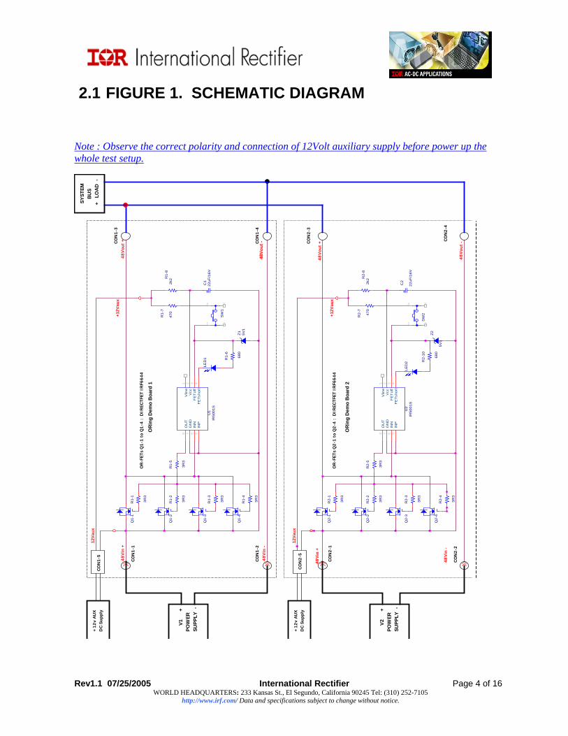
2.1 FIGURE 1. SCHEMATIC DIAGRAM Note : Observe the correct polarity and connection of 12Volt auxiliary supply before power up the whole test setup.
R1-
2
3R3
R1-
3
3R3
R1-
4
3R3
Z1
5V1
Vlin
e1
Vcc
2
FE
Tof
f3
FE
Tsh
ort
4IN
P5
INN
6G
ND
7O
UT
8
U2
IR50
01S
LED
2
1
4
2
3
SW
2
R2-
82k
2
C2
22uF
/16V
+12V
aux
12Va
ux
+12V
aux
12Va
ux
48
Vin
-
48
Vin
+
CO
N1
-5
48
Vou
t +
OR
-FET
s Q
1-1
to
Q1
-4 :
DIR
ECTF
ET I
RF6
64
4
CO
N1
-1
CO
N1
-2C
ON
1-4
CO
N1
-3
48
Vou
t -
R1-
82k
2
CO
N2
-5
48
Vou
t +
OR
-FET
s Q
2-1
to
Q2
-4 :
DIR
ECTF
ET I
RF6
64
4C
ON
2-1
CO
N2
-2
CO
N2
-4
CO
N2
-3
Q2-
2
Vlin
e1
Vcc
2
FE
Tof
f3
FE
Tsh
ort
4IN
P5
INN
6G
ND
7O
UT
8
U1
IR50
01S
LED
1
1
4
2
3
SW
1
Q2-
1
R1-
7
470
R2-
7
470
Q2-
4
Q2-
3
C1
22uF
/16V
Q1-
2
R2-
1
3R3
R2-
5
3R3
Q1-
1
R1-
6
680
R2-
10
680
R2-
2
3R3
R2-
3
3R3
Q1-
4
R2-
4
3R3
Q1-
3
R1-
1
3R3
Z2
5V1
R1-
5
3R3
48
Vin
+
48
Vin
-
+1
2v
AU
XD
C S
upp
ly
V
1
+P
OW
ERSU
PP
LY -
OR
ing
Dem
o B
oard
2
OR
ing
Dem
o B
oard
1
+1
2v
AU
XD
C S
upp
ly
V
2
+P
OW
ERSU
PP
LY -
48Vo
ut -
SY
STEM
B
US
+ L
OA
D -

Rev1.1 07/25/2005 International Rectifier Page 5 of 16 WORLD HEADQUARTERS: 233 Kansas St., El Segundo, California 90245 Tel: (310) 252-7105
http://www.irf.com/ Data and specifications subject to change without notice.
2.2 IRAC5001-HS48V Demo Board Pictures
Figure2A. Front side of the IRAC5001-HS48V Demo Board
Figure2B. Back side of the IRAC5001-HS48V Demo Board
IRAC5001-HS48V ORING DEMO BOARD REV1.0
48 Vout + 48 Vin – 48 Vout –
48 Vin +
Rev1.1 07/25/2005 International Rectifier Page 6 of 16 WORLD HEADQUARTERS: 233 Kansas St., El Segundo, California 90245 Tel: (310) 252-7105
http://www.irf.com/ Data and specifications subject to change without notice.
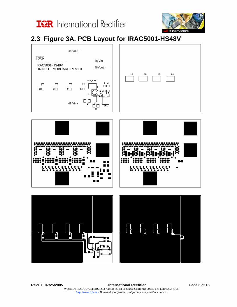
2.3 Figure 3A. PCB Layout for IRAC5001-HS48V 48 Vout+
48 Vin - 48Vout -
48 Vin+
IRAC5001-HS48V ORING DEMOBOARD REV1.0
+

Rev1.1 07/25/2005 International Rectifier Page 7 of 16 WORLD HEADQUARTERS: 233 Kansas St., El Segundo, California 90245 Tel: (310) 252-7105
http://www.irf.com/ Data and specifications subject to change without notice.
2.4 Bill of Material (BOM) for IR5001-HS48V Active OR-ing Demoboard
Item Total Circuit Value Component Manufacturer PN QTY Code Description 1 4 R1, R2, R3, R4 3R3 , 0.1W SMD, 0805 Thick film resistor 5% 2 1 R5 3R3 , 0.1W SMD, 0805 Thick film resistor 5% 3 1 R6 680 ohm, 1/10W SMD, 1206 Thick film resistor 5% 4 1 R7 470 ohm, 1/10W SMD, 1206 Thick film resistor 5% 5 1 R8 2.2k/ 1/10W SMD, 1206 Thick film resistor 5% 6 1 C1 22uF / 16V SMD, electrolytic capacitor ECEV1CA220SR 7 1 U1 IR5001S SMD, SOIC8 ORing Controller IC IR 8 1 Z1 5.1V / 0.5W SMD, 5.1 volt Zener diode BZV55-C5V1 9 1 LED SMD, TLSU1008 10 4 Q1, Q2, Q3, Q4 IRF6644 SMD, 100V 11mOhm DirectFET IR 11 1 Fetchk SW1 SMD , normally open B3S-1002 push button micro switch
12 1 PCB 13 1 Con5 2-pin connector
14 1 HTSNK 50.8x13.5x4.8 (mm) (Aavid Thermaloy)
437178 15 1gm. (Loctite) Thermal adhesive 383
3.0 CIRCUIT OPERATION The diagram in Figure 1 shows the test setup to evaluate the functionality of this demo board in each of 48Volt power supply output connected to the system bus load. The power load can be a single high power E-load (~3kW) or composed of several medium power E-loads connected in parallel. At least 2 units of high power converter - each capable of sourcing 100Amp is required to check the OR-ing functionality. Each converter should have an output voltage setting of 48V ( +/- 0.01 V ) to simulate a near balanced current sharing condition, and each output is link to the bus by one demo board- individually powered by a floating 12Volt DC supply ( bias voltage) through connector CON5. This connector route the positive bias voltage to the IC’s pin 7 (Vcc : < 13.9Vmax) and the negative bias to the output rail connector (Con1) of the power converter. This is necessary to drive the gates of 4 IRF6644 OR-FETs in parallel linking the highside (or positive output rail) to the positive of the bus. The negative rails of all power converters are all connected together to the negative rail of the bus.
Since this is a high current test setup, extra care should be observed in proper connections on the board to avoid unnecessary contact resistance which may further add heat to the board itself.
As a general design practice in choosing the appropriate mosfets, they must have low Rdson and the Vsd generated should be at least ~50mV when the OR-FET is “ON”.

Rev1.1 07/25/2005 International Rectifier Page 8 of 16 WORLD HEADQUARTERS: 233 Kansas St., El Segundo, California 90245 Tel: (310) 252-7105
http://www.irf.com/ Data and specifications subject to change without notice.
3.1 FETCHK FEATURE Ensure the test setup is correct and both power converters and OR-ing boards are in good condition before starting-up. For safe initial test, it is recommended to power up the OR-ing boards first with system load preset to less than 10Amps as startup load before doing the full load test. The thermal performance should be acceptable at room temperature testing even if the OR-ing board has no heatsink but do not press one or both FETSW for too long . This test will force the circuit to conduct the total load current through the body diodes of the OR-FET which will increase the heat dissipation at a very fast rate; thus extra precaution must be observed during this FETCHK test. The board takes advantage of a unique feature that comes with the IR5001 IC to assess the redundancy status of the system as well as the functionality of the OR-ing mosfets as a group (OR-FET1 or OR-FET2). Referring to Figure 6, the FETCHK feature enables the system designer to manually switch OFF the IC’s Vout pin ( gate drive) by pressing a normally-open microswitch “FETCHK SW1/ 2”. This switch link the +12V_aux thru R7 to the clamping zener Z1 (5.1V) in order to provide a logic voltage of ~5V (with reference to the IC’s GND ( pin (7)) to FETCHK/OFF pin 3. The desired outcome if FETCHK is initiated (while the OR-FET is ON) is to toggle OFF the output of the IC, which will turn-off the OR-FET. This will result in an increase of Vsd of more than 0.3V and a comparator inside will compare it to a 0.3V reference voltage. The internal comparator will turn-ON an open-drain mosfet to pull down pin 4 (FETSHORT pin), providing a ground path for the LED to light up. 3.2 SHORT CIRCUIT TEST During a fault condition such as short circuit of one of the converter, a finite amount of reverse current in the form of short duration negative current spike will occur just before the OR-FET completely turn-off. The peak of this reverse current is dependent on how fast the controller circuit switches off the OR-FETs during this fault condition. The IR5001 IC is capable of sourcing and sinking 3Apk to fast turn - ON or OFF of the OR-FETs. If short circuit occur at the secondary side of any power converter unit before the Active OR-ing circuit, this faulty unit will be isolated by turning-off the OR-FET(s) as quickly as possible, preventing the faulty unit from further drawing any current from the other remaining good power converter(s) connected in the system bus. It is recommended to initially set the E-load to minimum and set the current limit of the converters to ~120Amp before the evaluation of the reverse current during short circuit test.
Caution : Use appropriate size of shorting wire ( larger than #10 AWG with thick insulation) when performing short circuit test. Shorting V1 or V2 should be done very quickly. It is recommended to use a DC high current probe with amplifier initially set to >50A/V to avoid overloading the probe or the amplifier on the first test trial.
Rev1.1 07/25/2005 International Rectifier Page 9 of 16 WORLD HEADQUARTERS: 233 Kansas St., El Segundo, California 90245 Tel: (310) 252-7105
http://www.irf.com/ Data and specifications subject to change without notice.
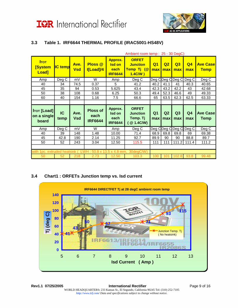
3.3 Table 1. IRF6644 THERMAL PROFILE (IRAC5001-HS48V)
3.4 Chart1 : ORFETs Junction temp vs. Isd current
IRF6644 DIRECTFET Tj at 28 degC ambient room temp
41
67 71
93 115
5043
0
20
40
60
80
100
120
140
5 6 7 8 9 10 11 12 13Isd Current ( Amp )
Tj (d
eg C
)
Junction Temp. Tj ( No heatsink)
Ambient room temp : 25 - 30 DegC)
ITOT
[System Load]
IC temp Ave. Vsd
Ploss @ I[Load]/4
Approx. Isd on each
IRF6644
ORFET Junction
Temp Tj (@ 1.4C/W )
Q1 max
Q2 max
Q3 max
Q4 max
Ave Case Temp
Amp Deg C mV W Amp Deg C Deg C Deg C Deg C Deg C Deg C40 34 74.5 0.37 5 41.2 40.2 41.1 41 40.3 40.6545 35 94 0.53 5.625 43.4 42.3 43.2 42.2 43 42.6850 38 108 0.68 6.25 50.3 49.4 52.3 46.6 49 49.3360 40 154 1.16 7.5 66.6 65 63.5 62.3 62.5 63.33
ITOT [Load] on a single
board
IC temp
Ave. Vsd
Ploss of each
IRF6644
Approx. Isd on each
IRF6644
ORFET Junction Temp. Tj
( @ 1.4C/W)
Q1 max
Q2 max
Q3 max
Q4 max
Ave Case Temp
Amp Deg C mV W Amp Deg C Deg C Deg C Deg C Deg C Deg C40 39 148 1.48 10.00 71.4 68.9 69.8 69.8 69 69.3845 42.8 190 2.14 11.25 92.7 89.9 90 90 88.8 89.750 52 243 3.04 12.50 115.5 111 111 111.2 111.4 111.2
with 1pc. extruded heatsink ( LWH : 50.8 x 13.5 x 4.8 mm, 30degC/W)50 52 218 2.73 12.50 103.3 100 101 102.8 93.8 99.48

Rev1.1 07/25/2005 International Rectifier Page 10 of 16 WORLD HEADQUARTERS: 233 Kansas St., El Segundo, California 90245 Tel: (310) 252-7105
http://www.irf.com/ Data and specifications subject to change without notice.
3.5 Chart2 : ORFET Conduction Loss vs. Drain current (Isd)
3.6 Heatsink Mounting Pictures
Figure 3B. Mounting of heat sink at the back side
Figure 3C. Side view with heatsink
P loss
2.0
2.7
1.5
1.48
2.14
3.04
0.0
0.5
1.0
1.5
2.0
2.5
3.0
3.5
4 5 6 7 8 9 10 11 12 13 14
Isd per ORFET ( AMP )
Con
duct
ion
Loss
= V
sd x
Tot
al L
oad
Cur
rent
/4(W
)Single board with heatsink
Single Board -No heatsink
Rev1.0 7/25/2005 International Rectifier Page 11 of 18
WORLD HEADQUARTERS: 233 Kansas St., El Segundo, California 90245 Tel: (310) 252-7105 http://www.irf.com/ Data and specifications subject to change without notice.
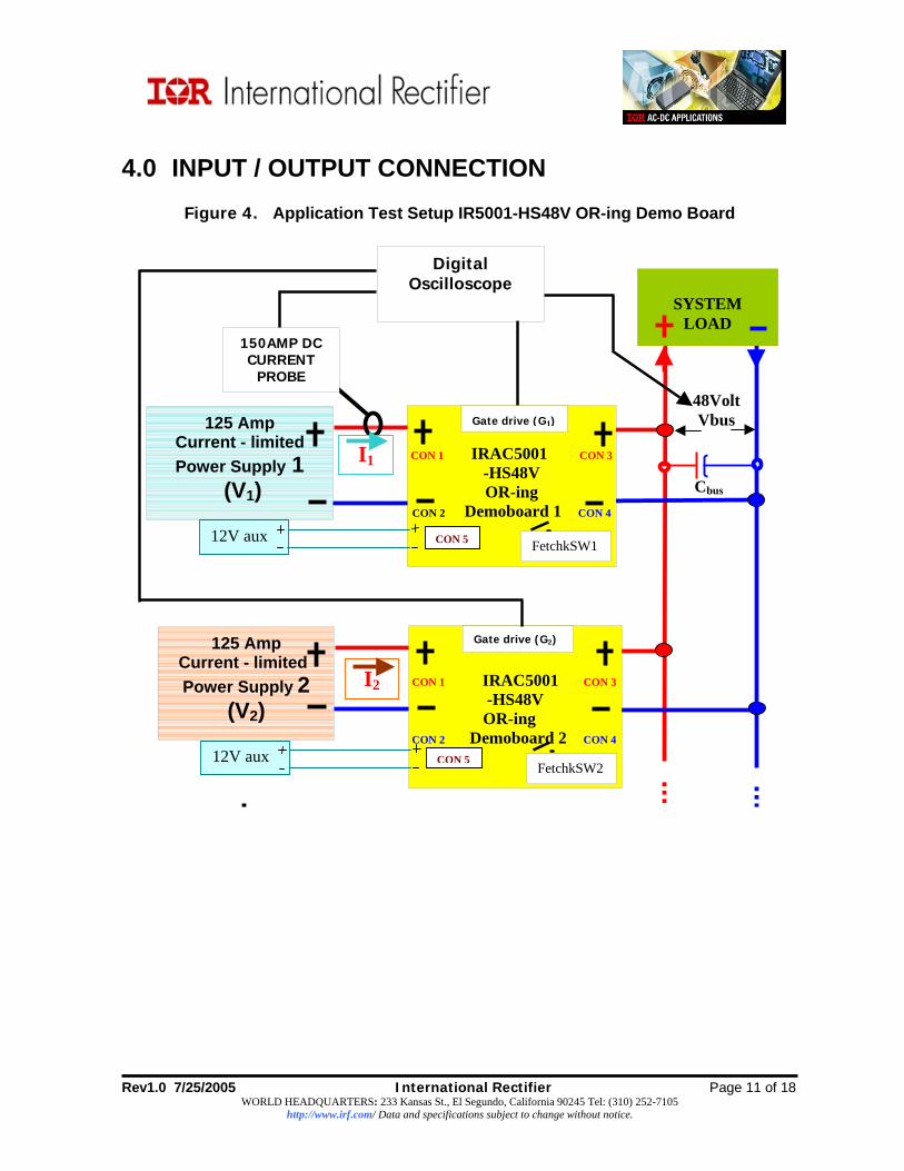
4.0 INPUT / OUTPUT CONNECTION
Figure 4. Application Test Setup IR5001-HS48V OR-ing Demo Board
CON 1 IR5001 CON 3
OR-ing CON 3 Demoboard N CON 4
125 Amp Current - limited Power Supply
12V aux
In
FetchkSWn
Gate drive (Gn)
CON 5
SYSTEM
LOAD 150AMP DC CURRENT
PROBE
Digital Oscilloscope
48VoltVbus
CON 1 IRAC5001 CON 3
-HS48V OR-ing
CON 2 Demoboard 1 CON 4
125 Amp Current - limited Power Supply 1
(V1)
12V aux FetchkSW1
Gate drive (G1)
CON 5
CON 1 IRAC5001 CON 3
-HS48V OR-ing
CON 2 Demoboard 2 CON 4
125 Amp Current - limited
Power Supply 2 (V2)
12V aux
I2
FetchkSW2
Gate drive (G2)
CON 5
I1
Cbus

Rev1.0 7/25/2005 International Rectifier Page 12 of 18
WORLD HEADQUARTERS: 233 Kansas St., El Segundo, California 90245 Tel: (310) 252-7105 http://www.irf.com/ Data and specifications subject to change without notice.
5.0 Short Circuit Test Setup
Figure 5. SHORT CIRCUIT TEST AND PATH OF THE REVERSE CURRENT . 6.0 Table 2 Truth table for IR5001 “FET Check Feature”
Case LED Initial During the CHK OR-FET
1 OR-FET
2 Comment
A off on 1 B off off
Vsd of FET 1 > 300mVVsd of FET 2 < 300mV Good N/A V1 > V2 + 0.4V
A off on 2 B off on
Vsd of FET 1 > 300mVVsd of FET 2 > 300mV Good Good |V1 – V2| < 0.4V
Short N/A V1 > V2 + 0.3V A off off
At least one is short |V1 – V2| < 0.3V
3 B off off
Vsd of FET 1 < 300mVVsd of FET 2 < 300mV
N/A Short V2 > V1 + 0.3V
Short circuit test on V1
IRAC5001 -HS48V
Demoboard
SYSTEMLOAD
OR-FET2
V2
OR-FET1
V1Reverse Current
Normal Load Current direction
DC High Current Probe
IRAC5001 -HS48V
Demoboard
Cbus
Rev1.0 7/25/2005 International Rectifier Page 13 of 18
WORLD HEADQUARTERS: 233 Kansas St., El Segundo, California 90245 Tel: (310) 252-7105 http://www.irf.com/ Data and specifications subject to change without notice.
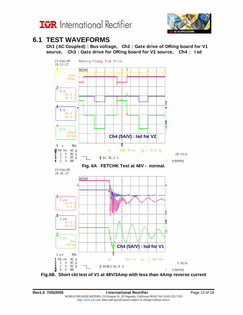
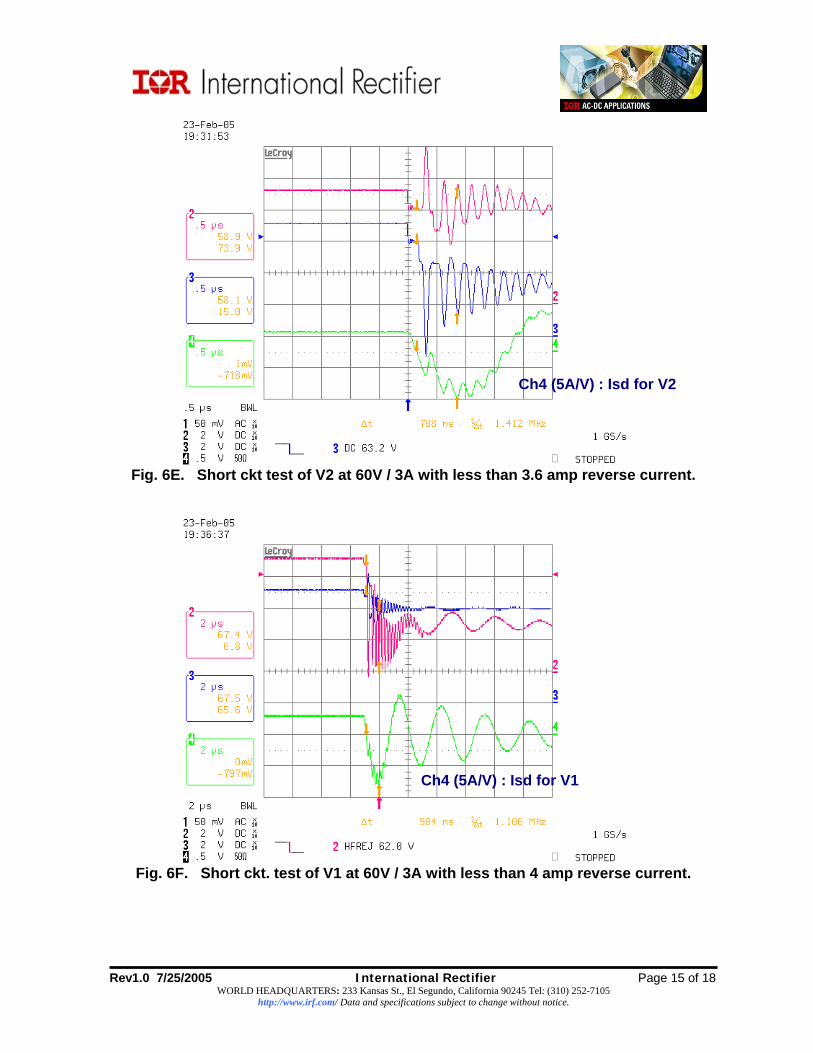
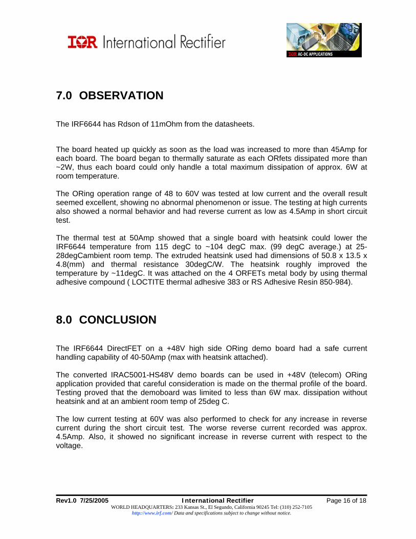
6.1 TEST WAVEFORMS Ch1 (AC Coupled) : Bus voltage, Ch2 : Gate drive of ORing board for V1 source, Ch3 : Gate drive for ORing board for V2 source, Ch4 : Isd
Fig. 6A FETCHK Test at 48V - normal.
Fig.6B. Short ckt test of V1 at 48V/3Amp with less than 4Amp reverse current
Ch4 (5A/V) : Isd for V2
Ch4 (5A/V) : Isd for V1

Rev1.0 7/25/2005 International Rectifier Page 14 of 18
WORLD HEADQUARTERS: 233 Kansas St., El Segundo, California 90245 Tel: (310) 252-7105 http://www.irf.com/ Data and specifications subject to change without notice.
Fig 6C. Short Ckt test of V2 at 48V / 3A with less than 3Amp reverse current.
Fig. 6D. FETCHK test at 60V - normal.
Ch4 (5A/V) : Isd for V2
Ch4 (5A/V) : Isd for V1
Rev1.0 7/25/2005 International Rectifier Page 15 of 18
WORLD HEADQUARTERS: 233 Kansas St., El Segundo, California 90245 Tel: (310) 252-7105 http://www.irf.com/ Data and specifications subject to change without notice.
Fig. 6E. Short ckt test of V2 at 60V / 3A with less than 3.6 amp reverse current.
Fig. 6F. Short ckt. test of V1 at 60V / 3A with less than 4 amp reverse current.
Ch4 (5A/V) : Isd for V2
Ch4 (5A/V) : Isd for V1
Rev1.0 7/25/2005 International Rectifier Page 16 of 18
WORLD HEADQUARTERS: 233 Kansas St., El Segundo, California 90245 Tel: (310) 252-7105 http://www.irf.com/ Data and specifications subject to change without notice.
7.0 OBSERVATION The IRF6644 has Rdson of 11mOhm from the datasheets. The board heated up quickly as soon as the load was increased to more than 45Amp for each board. The board began to thermally saturate as each ORfets dissipated more than ~2W, thus each board could only handle a total maximum dissipation of approx. 6W at room temperature. The ORing operation range of 48 to 60V was tested at low current and the overall result seemed excellent, showing no abnormal phenomenon or issue. The testing at high currents also showed a normal behavior and had reverse current as low as 4.5Amp in short circuit test. The thermal test at 50Amp showed that a single board with heatsink could lower the IRF6644 temperature from 115 degC to ~104 degC max. (99 degC average.) at 25-28degCambient room temp. The extruded heatsink used had dimensions of 50.8 x 13.5 x 4.8(mm) and thermal resistance 30degC/W. The heatsink roughly improved the temperature by ~11degC. It was attached on the 4 ORFETs metal body by using thermal adhesive compound ( LOCTITE thermal adhesive 383 or RS Adhesive Resin 850-984). 8.0 CONCLUSION The IRF6644 DirectFET on a +48V high side ORing demo board had a safe current handling capability of 40-50Amp (max with heatsink attached). The converted IRAC5001-HS48V demo boards can be used in +48V (telecom) ORing application provided that careful consideration is made on the thermal profile of the board. Testing proved that the demoboard was limited to less than 6W max. dissipation without heatsink and at an ambient room temp of 25deg C. The low current testing at 60V was also performed to check for any increase in reverse current during the short circuit test. The worse reverse current recorded was approx. 4.5Amp. Also, it showed no significant increase in reverse current with respect to the voltage.