ion iplantation of wide banogap semiconductors. (u) …
TRANSCRIPT

ION IPLANTATION OF WIDE BANOGAP SEMICONDUCTORS. (U)
M N' ,E 1AY 80 K W VAIDYANATHAN, C L ANDERSON N00173-79-C-0028WICLASSIFIED ML

111112.2- '~ IL6
Iff'111111. 6
MICROCOPY RESOLUTION TEST CHART

ION IMPLANTATION OF WIDEBANDGAP SEMICONDUCTORS
K. V. Vaidyanathan, C. L. Anderson, H. L. Dunlap, and R. A. Jullens
Hughes Research Laboratories
3011 Malibu Canyo'n-1Ioad
Malibu, CA 90265
May 1980 C3
Contract N00173-79-C-0028
Final Report
For period 15 December 1978 through 14 December 1979
Approved for public release,- distribution unlimited.
Sponsored by
NAVAL ELECTRONICS SYSTEMS COMMAND
Department of the Navy
Washington, D. C. 20375
Monitored by
NAVAL RESEARCH LABORATORY4555 Overlook Avenue, S. W.
0 Washington, D. C. 20375
,..
8.0 9 12 03(

UNCLASSIFIEDSECURIY CLASSIFICAION OU THInS PAGE (WhI Osl ae ,te"E)_________________
REPOR DOCUMENTATION PAGE READE INSUTIOS
MU . GOVT ACCESSION NO. 3. RECIPIENTIS CATALOG 0 -0860t
________Amy
JONMPLNTAIONOF IDEBANGAPFina1lep0tSEMONDPATTON FWIEBNDA 15 Dec 078 - 14 Dec 79,
7. AUTHOR(~ .~M~C A.T~a
KV./Vaidyanathan2Th. L./Anderson ; Nnd73-79-C-,.H.L. Dunap4 o R.A.Jullens/
JPE*RuIW ~ ~AREA & W.ORK UNIT NUMBERSHughes Research Laboratories3011 Malibu Canyon Road/Malibu, California 90265 _____________
11. CONTROLLING OFFICE NAME AND ADDRESSNaval Electronics Systems Command f/ May 408Department of the Navy *V-xTTWashington, D.C. 20375 49____________
'14. MONITORING AGENCY NAM4E a ADVRESSUI1 -ifne,v finm C...,er..II0e0a Officre) IS SECURIT Y CLASS. (of 8hJ2 ewportj
Naval Research Laboratory UCASFE4555 Overlook Avenue, S.W. UCASFEWashington, D.C. 20375 e'.& 1 iL'w~icATION DOWNGRADING
10. DISTRIBUTION STATEMENT (.0I Phi. Roppnng
Approved for public release; distribution unlimited.
I7. DISTRIBUTION STATEM4ENT 4 0 IA. abstfart ehfored in flI.,h 'Q. if diii.,.. a,, t N..Port)
IS. SUJPPLEMENTARY MOTES
19. KEY WORDS (I'C~ju 6" .. re"e it neres-av end #dPn"tiv 6V Wi'k "wu00c")
GaAs Ion Implantation
GaAs p-n JunctionsGaAs Bipolar Transistors
j a0. ASTRACT (Cenioawan r..ew.ol Wge fnecease mREidpotlll Sop Week pnowbt)
This report describes the development of a mask set and process technologyfor the fabrication of sequentially implanted p-n Junctions and bipolartransistors in GaAs. Development of high-density implant masks isdescribed. The electrical properties of the implanted p-n Junctions arereported, and the dominant leakage current mechanism is identified.
00 1 FOAM* 1473 EDITION Or I OVs5IS oeSOLETt UNCLASSIFIED
SECURITY CLASSIFICATION OF THIS PAGE gWhe. IN** EfoefV

TABLE OF CONTENTS
SECTION PAGE
1 INTRODUCTION AND SUMMARY. .... ............. 7
2 PROCESS DESIGN. .. .................... 9
A. Localized Implantation Studies .. ...... .. ..... 9
B. Photomask Design .. .................. 11
3 ION IMPLANTATION AND ELECTRICAL EVALUATIONSTUDIES. ......................... 29
A. Preliminary Electrical Evaluation ofImplanted Layers .. .................. 29
B. p-n Junction Fabrication and ElectricalEvaluations. ..................... 32
REFERENCES .. ....................... 49
WTIS
Me TAjB
3

LIST OF ILLUSTRATIONS
FIGURE PAGE
1 SEN photograph of a 1.5-jam-wide stripe formedby plasma etching of Ge deposited over siliconoxynitride on GaAs .. ................... 10
2 Flow chart of the processing steps involved formasked implants in GaAs. ................. 12
3 SEN micrograph of wafer after going throughthe lift-off process .. .................. 13
4 Level 0 mask .. ...................... 15
5 Level 1 mask .. ...................... 16
6 Level 2 mask .. ...................... 17
7 Level 3mask .. ...................... 18
8 Level 4mask .. ...................... 20
9 Level 4' mask. ...................... 21
10 Level 5 mask .. ...................... 22
11 Level 5' mask. ...................... 23
12 Level 6 mask .. ...................... 24
13 Level 7mask .. ....................... 25
14 Level 8mask .. ....................... 26
15 Level 9mask .. ...................... 27
16 Level 10mask. ...................... 28
17 Theoretical design of a four-energy Be implantshowing the four Gaussian implant profiles andtheir summation. .. .................... 30
18 Carrier concentration profile obtained by C-Vmeasurements from a Be-implanted sampleannealed at 800*C, 30 mi.. ................ 31
19 Impurity profiles of Se and Be obtained fromSIMS measurements on wafer NRL-C.. .. ........... 33
5

FIGURE PAGE
20 Distribution of breakdown voltage for typicaldiodes in wafer NRL-B ... ... ................. ... 37
21 Distribution of breakdown voltage for typicaldiodes in wafer NRL-C ...... ................. ... 38
22 Current-voltage characteristics of 200-pm-diameterdiodes from wafer NRL-C ..... ................ ... 39
23 Current-voltage characteristics of 200-m-diameterdiodes from wafer NRL-C ..... ................. ... 40
24 Current-voltage characteristics of 100-jm-diameterdiodes from wafer NRL-C ..... ................ ... 41
25 Current-voltage characteristics of 400-1m-diameterdiodes from wafer NRL-C ..... ................ ... 42
26 Current-voltage characteristics of 200-m-diameterdiodes from wafer NRL-A...... .. .............. ... 45
27 Current-voltage characteristics of 200-jm-diameter
diodes from wafer NRL-B .............. ...... .. 46
6

SECTION 1
INTRODUCTION AND SUMMARY
The primary objectives of this program are to study the electrical
properties and carrier distributions in ion-implanted and annealed GaAs
and to demonstrate the feasibility of forming planar, isolated p-n
junctions by sequential implantation of donors and acceptors into semi-
insulating GaAs. To fabricate such planar junctions, a selective area
implantation process technology was developed. The required device
isolation was achieved by exploiting the semi-insulating nature of
Cr-doped GaAs.
To perform selective area implantation (required in a planar
process), it is necessary to develop a suitable masking scheme such that
none of the dopants penetrate undesired regions of the wafers. The
simplest masking scheme would be to use a dielectric layer such as
silicon oxynitride (Six 0 yN 2) along with photoresist. However, to pro-
vide adequate masking for deep implants, excessively thick layers would
be required. Such thick layers would lead to severe photolithographic
problems, especially when fine pattern resolutions are required. During
the early phase of this program, a masking scheme consisting of silicon
oxynitride and germanium layers, both deposited by a plasma-enhanced
process, was developed. The germanium layer had to be plasma etched,
and the process had severe yield problems. Lift-off process are quite
simple and result in excellent yield even when the pattern dimensions
are micrometer sized. A lift-off process was developed to use Cr-Au
as an implant mask. This process is described in detail in
Section 2.
In designing the implants for p-n junction fabrication, it is nec-
essary to know the electrical properties of the doped layers. In par-
ticular, the lowest and highest concentrations of dopants that can be
activated in Cr-doped GaAs has to be known. We performed experiments to
determine these parameters. It is also necessary to evaluate the elec-
trical activation and the carrier mobilities on the device wafer itself.
We designed a versatile mask set to fabricate test structures, including
7

van der Pauw patterns for Hall-effect measurements, Schottky barriers
for capacitance-voltage (C-V) measurements, and p-n junctions with
different areas. The p-n junctions were characterized by measuring the
current-voltage (I-V) characteristics both in the forward and reverse
directions and the breakdown voltage of the devices. A detailed study
showed that surface leakage is the dominant leakage mechanism in these
planar diodes. The results of the electrical evaluation are discussed
in Section 3.
I
8!

SECTION 2
PROCESS DESIGN
The major aim of this program is to develop a reliable process
technology for fabricating planar, fully ion implanted, isolated p-n
junctions and bipolar transistors. Since these devices are to be iso-
lated, we decided early during this reporting period to exploit the
semi-insulating nature of the Cr-doped GaAs substrates to provide the
required isolation between the devices. This section discusses experi-
ments performed to develop a localized implantation capability and the
mask set used to fabricate these devices.
A. LOCALIZED IMPLANTATION STUDIES
Before planar isolated p-n junctions can be formed, a masking scheme
must be developed that will prevent ions from penetrating regions where
they are not wanted. A dielectric layer such as SiO2 or Si3N4 along with
a layer of photoresist formed by conventional lithography could be used as
a simple mask. The major problem with this approach is the rather low
stopping power of both layers. This is especially a problem when one
w~shes to form deep layers, and those as required for vertical bipolar
transistors. Masking deep layers would require using excessively thick
oxide or PR layers. The use of such thick films frequently results in
poor pattern definition. We believe that the use of thin films of a
denser material will alleviate this problem and that such a thin film
will serve adequately as an implant mask.
We have developed a process that utilizes plasma-deposited layers
of silicon oxynitride and germanium. Conventional photolithographic
techniques are used, and the germanium layer is plasma etched. An SEM
photograph of a processed sample is shown in Figure 1. The sample has
a strip 11.5 pm wide where the Ge has been etched off; the nearly ver-
tical sidewall is visible. The yield of this process is, however, poor.
The poor yield coupled with the necessity of using relatively thick Ge
layers makes it attractive to use heavy metals such as Au, W, or Au-Cr
for masking.
9

8893-10
Figure 1. SEM photograph of a 1.5-lim-wide stripe formed by plasmaetching of Ge deposited over silicon oxynitride onGaAs. The silicon oxynitride-germanium layer will beused as an implant mask.
10

Severe problems were encountered, however, in lifting Cr-Au or Au
when the metal was directly evaporated onto a thin dielectric layer.
The use of an intermediate layer of Al during the lift-off procedure
resulted in an acceptable yield from the process. The process is
described below, and the major processing steps are shown in Figure 2.
First, the wafer is cleaned with solvents and etched in an
H2 :H 202:NH4OH (480:4:10) etch for 5 min. This removes %I pm from the
surface while maintaining a smooth, shiny appearance. A silicon oxy-
nitride film, 1u400 X thick, is then deposited on the wafer at 350°C by
the plasma-enhanced deposition (PED) process using the LFE PND-301
system. A layer of photoresist (Shipley 1350J) is spun on the oxide
layer followed by 3000 X of Al. Following a photoresist and exposure
step using an appropriate light field mask, the Al layer is etched in
an H 3PO4 :CH 3COOH:HNO 3:H 20 (76:6:3:15) etch at %400 C for ,1.5 min. Fol-
lowing the Al etch, the underlying photoresist layer is exposed, typi-
cally for 1.5 min, to ensure considerable undercutting of the resist.
This is followed by evaporation of '200 A of Cr and then of Au to a total0
thickness of '15000 A. The process is completed by lift-off of the Cr-Au
composite. The process is highly reproducible and results in acceptable
yield. SEM micrographs of the wafer after going through the process are
shown in Figure 3.
B. PHOTOMASK DESIGN
We have designed a versatile mask set for this program. This
section, with the aid of accompanying photographs, describes it in
detail.
The mask set allows us to perform three localized sequential
implants, as is required for fabricating fully ion implanted planar
isolated bipolar transistors. The mask set has provisions for making
Hall-effect and C-V evaluations of each implanted layer. The process
can thus be evaluated at every step. This will help in correlating
device parameters with process variables. Diodes with 25, 50, 100, 200,
and 400 Pm diameters can be fabricated and formed either by the base-
collector or the base-emitter implants. Field-effect transistors (FETs)
11

9703-10
GaAs f Ga&s WAFER WITH-400A
I SiXOYNZ
PR 1.5pmSiXOVN 2 ----- GaAs WAFER AFTER SPINNING
Gafs A THIN PR LAYER
PR - _ _ _ _ _ _ _ _ _ _ 00
PR AFTER- 31MCASOXOyNZ Al EVAPORATION
Gaft AND PR EXPOSURE
aA
PR AFTER A! ETCH AND__i_0__N_------_ PR PROCESS. NOTE
X Y ZTHE UNDERCUTTINGG~ft OF THE PHOTORESIST
Au-Cr 50Wm
Six~y~z~AFTER LIFOFFA
GaAs -
________________jREADY FOR IMPLANT
Figure 2. Flow chart of the processing steps involved formasked implants in GaAs.
12

Figure 3. SFM micrograph of waferaft er going t hrough t helift-off process.

can be fabricated with this set as well as patterns for evaluating the
contact resistance of Ohmic contacts. There is also a pattern for check-
ing for any surface conversion effects by evaluating the resistance
between adjacent implanted regions. The masks are described below in
detail.
1. Level 0
The mask shown in Figure 4 represents the initial level in the mask
set. The pattern consists of one large etched region per chip and is
useful for visually aligning the chip. It will be particularly useful
if a technique such as laser processing is used for forming Ohmic con-
tacts. There is also another alignment mark; it is etched into GaAs and
will serve as a marker for subsequent alignments.
2. Level 1
The level I mask, shown in Figure 5, is the first operational mask
and will be used for collector implants. Regions that are clear in this
mask as shown are regions where the implant mask material is present.
Elements in this mask include a Van der Pauw Hall pattern, a segment
for C-V measurements, and collector implants for transistors and diodes.
3. Level 2
The level 2 mask, shown in Figure 6, serves as the base implant
mask for bipolar transistors. This level also includes selective
implant areas for Hall and C-V evaluations.
4. Level 3
The level 3 implant mask, shown in Figure 7, serves as an emitter
implant mask. Note that this level also allows for increasing the
surface concentration in the Ohmic-contact regions for the collector
and in the C-V analysis segments.
After the emitter implant, the sample is ready to be annealed with
or without an encapsulant.
14

8893-1
U
Figure 4. Level 0 mask. This will be used for etching
alignment marks in the substrate.
15

083-2
I 4s01
-niU. *I
* 6*too
Figure 5. Level 1 mask. Implantation mask for collector-lmplants.The dark regions in the mask will receive the collectorimplant.
16

8893-3
m m
* 99I 9
Figure 6. Level 2 mask. Base implant mask.
17

" . 0 o 8093-4
'-,00 U
.' - -.e •"40
(~*.0.~0, -
Figure 7. Level 3 mask. This will be used for emitterand collector contact region implant.
18

5. Levels 4 and 4'
The level 4 mask, shown in Figure 8, defines the Ohmic-contact
metalization in regions that have r.. eived base implants. These regions
can be defined either by lift off or chemical etching. If chemical
etching is used in subsequent steps, mask 4' (Figure 9) will be used
to protect the base contact metal.
6. Levels 5 and 5'
The level 5 mask (Figure 10) defines the metalization to regions
which have received collector and emitter implants. Mask 5' (Figure 11)
assures that these metalized regions are protected during subsequent
processing if the metal is chemically etched off in Level 6. Also,
during steps 4 and 5, the contact evaluation patterns are defined. This
will allow us to evaluate the nature of the Ohmic contacts.
7. Level 6
This mask (Figure 12) allows us to define the Schottky barriers
for performing C-V evaluations. There are two Schottky diodes with
different areas. Also, the gate metalization is defined for forming
the FETs. Levels 4, 5, and 6, along with 4' and 5', are designed to
take into account that different metalizations have to be used for
making Ohmic contacts to p and n regions and for forming a Schottky
barrier.
8. Level 7
In fabricating sealed junctions, the junctions must be passivated
with a suitable glassy dielectric. After this layer has been deposited,
Mask 7 (Figure 13) can be used to open holes for making contact to
the base metal.
19

8893-5
mas 0
*~ Q90
Figure 8. Level 4 mask. This will be used for contactmetalization to base regions.
20
• QO A

Saga-.
0
00
- I0
0
Figure 9. Level 4' mask. To protect base metalizationduring subsequent processing, especially ifchemical etching is used to define the metaliza-tion pattern.
21

* s n1093-7
E l 3nnng
00u00 00 1E) Eu.' X
E
0 0
€0. EE* I'-
mm
.000
o~s sol
s 0.
Figure 10. Level 5 mask. Collector-emitter metalization mask.
22

8093-8
0 .0
00
Figure 11. Level 5' mask. Useful for protecting collector-emitter metalizations during subsequent processing.
23

8893-9
Figure 12. Level 6 mask. Used for forming Schottky-barrierinetalization.
24

6693-10
* 0 0
dlU
Fiur 13 Lee 7 akIsd o pnn hlsi hglsydeeti0asvainlyrt otc
the bse mtaliztio0
02

9. Levels 8 and 9
The masks used in levels 8 and 9 (Figures 14 and 15) are used to
open holes in the insulator to make contacts with the emitter/collector
metalization and to the Schottky-barrier metalization, respectively.
10. Level 10
This mask (Figure 16) allows the various metalized regions to be
brought to the bonding pads.
|a~i~i B| B 603-Il
- 0
* I•|i lN
n n
00
Fir "14 Lee 8 makmsdfrfrin h ilcrcteie-olc metaiza i
:•.. 26010i U.i U
- Sm
Fiue14 eel8msk sd o oxn hedeecrcte0te-olcormtlztos
260
01 . . n - " 1 . . . ... . i m . .. .. .. I .. . . . I I II I I . . .. . .. - - , , 0.

8893- 12
Nis
El
ml.
U
Figure 15. Level 9 mask. Used to open holes in the dielectricto the Schottky-barrier metalization.
27

8093-13
0.- t l
- II
!!!! .. i..4@6
0000
Figure 16. Level 10 mask. This mask will allow us to connectthevarious metalized regions to bonding pads.
28

SECTION 3
ION IMPLANTATION AND ELECTRICAL EVALUATION STUDIES
This section describes the implantation and electrical evaluation
of the implanted layers and the p-n junctions. Preliminary experiments
on implantation performed in the early phase of this work are described
in Section 3.A. Section 3.B discusses the electrical evaluation of p-n
junctions formed in semi-insulating GaAs by sequential ion implantation
of Se and Be.
A. PRELIMINARY ELECTRICAL EVALUATION OF IMPLANTED LAYERS
To design ion implanted p-n junctions, it is necessary to know the
apparent electrical activation of the implanted species, the carrier
mobility, and the carrier distribution in the implanted layers. All of
these parameters are influenced by several factors, including the
annealing environment and the encapsulant used. Consequently, the elec-
trical properties of Be- and Se-implanted layers were studied.
Be is an efficient acceptor dopant and, for concentrations at or18 -3
below 3 to 5 x 10 cm , the Be distribution after annealing is not
significantly different from the as-implanted distribution. This pro-
vides an upper limit of I to 2 x 1018 cm- 3 on the maximum Be concentration
that can be used without risking having severe redistribution effects take
place. To estimate the minimum acceptor concentration that can be effi-
ciently activated, a multiple energy implant scheme was designed and the16 -3
doses varied to achieve Be concentrations ranging from 3 x 10 cm to17 -3
1 x 10 cm . The theoretically calculated distribution is shown in
Figure 17. Table 1 shows the electrical activation data obtained from
samples annealed at 800C using our patented melt controlled ambient2
technique (MCAT). Figure 18 shows the carrier concentration profile as
measured by C-V measurements on a sample implanted to a uniform concen-17 -3
tration of 10 cm and annealed at 8000 C for 30 min.
29

im
0~4.
0
S0
-4
0.d 0
44
r. f-W
-H 0
r-4 'A
4)0
0
r-4
*d
300
* mom

Table 1. Electrical Properties of Low-ConcentrationBe-Implanted Layers. MCAT Annealed at 800°C
Hole ApparentSheetDesired Concentration, Mobility, Electrical
-3Resistivity, 2 V 1 1 Activation,cm W/O cm Vsec-
1017 1630 ± 90 230 ± 8 94 ± 8
1165 x 6270 ± 1700 235 ± 14 50 ± 10
3 x 10¹⁶ 44,000 170 %16
3 9793-
2
654
L 3W 2
10169 -
7654
3x10 1 5 I I I I0 0.1 0.2 0.3 0.4 0.
DEPTH, an
Figure 18. Carrier concentration profile obtained by C-V measurementsfrom a Be-implanted sample and annealed at 800*C, 30 min.
The as-implanted calculated profile is shown inFigure 17.
31

It is well known that Se is a well-behaved donor in GaAs and
can be efficiently activated. Previous work performed at this and other
laboratories has demonstrated that low fluence, room-temperature
Se implants can be effectively activated. However, to achieve high
donor concentrations using Se, elevated temperature implants will be+
required. For ease in processing, we decided to fabricate a p -n struc-
ture by sequential implantation of selenium and beryllium. The electrical
properties of the implanted layers and the current-voltage characteristics
of the junction devices are described in the following section.
B. p-n JUNCTION FABRICATION AND ELECTRICAL EVALUATIONS
After developing the selective masking technology, three different
wafers of Cr-doped, semi-insulating GaAs were subjected to sequential
implants to fabricate p-n junctions. A deep n-type layer was first
implanted, followed by a shallower p-type layer. For n-type doping, Se
was used as the dopant of choice, while for p-type doping, Be was used
as the dopant. To make the analysis easier, a multiple energy implant
scheme was designed to provide a uniform concentration for the n-type
layer. Table 2 provides the implant energies and fluences used for the
three wafers designated NRL-A, B, and C. In all cases, the Be implant13 -2
energy and dose were kept constant at 25 keV and 1.5 x 10 cm
respectively. The samples were annealed at 850 0C for 30 min with silox
encapsulant. Figure 19 shows the impurity profiles of implanted Be and
Se obtained by secondary ion mass spectrometry (SIMS) from wafer C.
Ohmic contacts to the n-type layers were formed by alloying evaporated
Au-Ge-Ni, while contacts to p-type layers were formed by alloying
evaporated Ag-Mn contacts. The alloying was performed at %350*C for
1 min in flowing forming gas. Hall-effect measurements were performed
on appropriate Van der Pauw patterns. The data from n-type implanted
layers are shown in Table 3, while data from p-type layers are shown in
Table 4. The implants were performed through 0400 X of Si 0 N depositedx y zby a PED process. We estimated that %20% of the implanted ions (both Be
and Se) come to rest within the silicon oxynitride layers. Using this
32

9763-11
25 k@V
10181.5 x1013 CMf 2
z0
400 k9V 7A x 1012 CM2
150ko.V 25x 1012 -m2
1017
1016 10 500 1000 1500 2000 2500 3000
DEPTH (A)
Figure 19. Impurity profiles of Se and Be obtained from SIMS measure-
ments on wafer NRL-C.
33
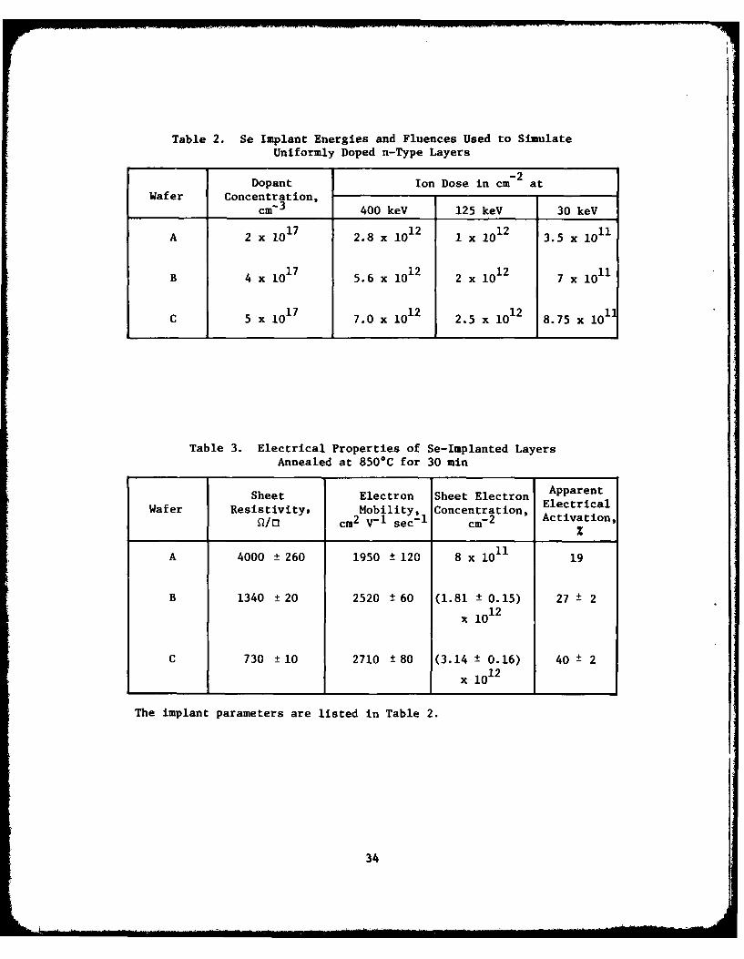
Table 2. Se Implant Energies and Fluences Used to SimulateUniformly Doped n-Type Layers
-2Dopant Ion Dose in cm at
Wafer Concentration,cm 3 400 keV 125 keV 30 keV
A2 x 1017 2.8 x 101 2 1 x 10¹² 3.5 x 101 1
4 x 101 7 5.6 x 101 2 2 x 10¹² 7 x 10¹¹
C5 x 101 7 7.0 x 10¹² 2.5 x 10¹² 8.75 x 101
Table 3. Electrical Properties of Se-Implanted LayersAnnealed at 850 0C for 30 min
Sheet Electron Sheet Electron Apparent
Wafer Resistivity, Mobility, Concentration, Electrical
0/0 cm2 V- 1 sec-1 cm-2 Activation,
A 4000 ± 260 1950 ± 120 8 x 10 1 1 19
B 1340 ± 20 2520 ± 60 (1.81 ± 0.15) 27 ± 2
x 1012
C 730 ±10 2710 ±80 (3.14 ± 0.16) 40 ± 2
x 1012
The implant parameters are listed in Table 2.
34

Table 4. Electrical Properties of Be-Implanted LayersAnnealed at 850°C for 30 min
Sheet Hole Sheet Hole ApparentElectricalWafer Resistivity, Mobility, Concentration, Activation,
cm2 V-1 sec-i cm
A 5600 250 180 2 (6.2 ± 0.2) 52 2
x 1012
B 4600 - 60 200 _ 1 (6.75 ± 0.2) 56 + 2
x 1012
C 4180 ± 170 206 - 1.5 (7.25 ± 0.2) 60 + 2
x 1012
The implant energy was 25 keV and the fluence used was 1.5 x 1013 cm- 2
The effective fluence was reduced to 1.2 x 1013 cm- 2 because of ionsstopped in the oxynitride layer.
35
L ZI " - '' . ............. ....

estimate, it is apparent that very high electrical activation has been
achieved in all cases. The mobilities were in the expected range.
After eliminating diodes tha were electrical shorts, the breakdown
voltages of several diodes were estimated using a curve tracer. Wafers
B and C were probed at random, and diodes with different diameters were
measured. Figures 20 and 21 show histograms of the breakdown voltage of
several diodes in wafers B and C, respectively. Diodes in wafer B
appear to have breakdown voltages in the range of 20 to 30 V, while in
wafer C most of the diodes exhibit breakdown voltages between 40 and 50 V.
For the concentration of donors in the n-region of the device, the esti-
mated breakdown should be between 20 to 30 V. Figures 22 through 25
show the I-V characteristics of several diodes from wafer C. Figures 23
and 24 show the I-V curves of diodes from wafer C. These diodes were
200 pm in diameter. The data were taken from diodes randomly selected
on the wafer. The forward characteristics of the diodes can be expressed
by the classical relation
I [e x ( ) " 1
The values of I° and n are listed in Table 5. The ideality factor
(n "x 2) clearly shows that the forward current is dominated by recom-
bination in the space-charge region.
Using the data from wafer C, we have calculated the ratios of
leakage currents at different bias voltages from a large number of 100-
and 200-jm-diameter diodes. The data are listed in Table 6. The leak-
age current ratio varies from 2.12 to 3. The ratio of the area of the
diodes is 4, while ratio of their perimeters is 2. It is thus clear
that a substantial fraction of the leakage current results from surface
leakage and is not a bulk phenomenon. Similarly processed devices with
suitable guard structures should exhibit even lower leakage.
The I-V characteristics typical of devices in wafers A and B are
shown in Figures 26 and 27, respectively. All diodes from wafer A
exhibit higher leakage at all voltages. The reasons for this are not
quite clear.
36

9793-2
12
11
10
9
8
w 7a0
a 60w* 5
z4
3
2
1 -
00 10 20 30 40 50
BREAK DOWN VOLTAGE (VOLTS)
Figure 20. Distribution of breakdown voltage for typical diodesin wafer NRL-B.
37

9793-3
14-
12
10
0
U.0
Cm6
z
4 L
2
0 10 20 30 40 50 60 70 > 70 V
BREAKDOWN VOLTAGE (VOLTS)
Figure 21. Distribution of breakdown voltage for typicaldiodes in wafer NRL-C.
38

9793-6
FORWARD BIAS 1VOL1M) -
16-7 0.2 0.4 0. 0.8 1.0 1.2 1.4V
10-8 1-
-9A W10 10-9 1zus
&U
IC 10-10 0o
10-11 290/M *DIODES 10-4
10 =1.43 x10⁻¹² A
n=2.01
4 a 12 16 20
REVERSE BIAS (VOLTS) --
Figure 22. Current-voltage characteristics of 200-im-diameter diodesfrom wafer NiL-C.
39

9793-4
FORWARD BIAS (VOLTS)-
0 0.2 OA 0.6 0.8 1.0 1.2 1A 17
10-
zz
10-11 -Ar~DOE 10- 0
Uj~~ IV1
dc 1 -10-8
0 4 6 12 i6 20 24
REVERSE BIAS (VOLTS)
Figure 23. Current-voltage characteristics of 200-.am-diameter diodes
from wafer NRL-C.
40

9793-6
FORWARD BIAS (VOLTS) -
062 0.4 0.6 0.8 1.0 1.2 1.4
I- 107 " 10-z w
LU u
M M
0 A VJ .6AUm
Ca 4r c
REES IA VLS
Fiur 24curn-otgecaatrsisofc0imdaeedide from0 wafer N0-
41

9793-7
FORWARD SIAS.(VOLTS)
Q.2 M. 0.6 0.8 1.0 1.2 1.4
110-8
U LUus CCcc
U, 0
10-9 10-7
10-10 401-400 m# DIODE
WAERI0 &O2 x10-12A
n=2.2
2 4 6 8 10 12
REVERSE BIAS (VOLTS)
Figure 25. Current-voltage characteristics of 400-pmu-diameter
diodes from wafer NRL-C.
42

Table 5. Comparison of Diode Parameters Obtained fromSequentially Implanted GaAs p-n Junctions
Diode Diameter, I , AWaerJm o0
A 400 4.3 x 12.3
1-12B 200 (1 ± 0.1) x 10 (1.7 ± 0.2)
400 (1.45 _ 0.05) (2.002 ± 0.001)
x 10- 12
C 200 (8.5 + 1.5) x 10- 1 3 2.1 + 0.02
400 (1.2 _ 0.2) x 10- 12 2.03 + 0.03
800 (9 4) x 10- 12 2.2 ±0.1
43

00
0 04 r- -0 C 0 000- 4 4 0 440 0
co 00 +1 C) 4 IrC1 0 1 1 +10 -I r-4 1 0 LA 0 - - 0
.4 x - x 2 4 . 0o 0 x- 0 -4 v-4 0
W 0 - 400 - -4 0 - 0 0--0 4 -*4 0 0
0: -4t vI In vI vI ON4 %D v-04 00 -4;C ! n 1 0 0*~
-V4 cc w v-I 04 +1 r -
w wI. 0 +1 01 01 +1 +1 +1 +0O w. +1 +1 +1 +
000 en CA en in enr A A 00 *d enI * . . *
LI4-4 N- OD CCA 0 -I -7 N C-. en co en v4
41I
CO0
00 w 0OtCd > .G ~ .7- 4-
0.-4 - 50.w 1 0 C
0l. cc0w 0 0 0 0 00 0 0 0 0 0 0 0 0>I 4 N C4 7 N1 04 t N4 %:r N4 -. -7 N N -.
4)v.
co
4.44

9793-8
FORWARD BIAS IVOLTS) -
la70.2 0.4 0.6 0. 1.0 1.2 -1.4
11r-
10-8 1-
z z2 wCccwU3
C~ 0.
la-11200 nt DIODES
I 0=1.4x10⁻¹² A
j= =4.3nA/an2
n =2.00
io-12, 10-9
4 8 12 i6 20
REVERSE BIAS (VOLTS) -5
Figure 26. Current-voltage characteristics of 20O-Um diameter
diodes from wafer NRL-A.
45

9793-9
FORWARD BIAS (VOLTS)-'.
ari 0.2 0. 0.6 0.8 1.0 1.2 1A
10-10- jo
z 5
IIA
10-i o-2O~r~DIODES
I= 4.3 x ir 1A
n= 2.3
16-101 10-6
REVERSE BIAS (VOLTS) -
Figure 27. Current-voltage characteristics of 200-jiu-diameter diodes from wafer NRL-B.
46

In conclusion, the electrical evaluation studies clearly show that
low-leakage, planar, isolated p-n junctions exhibiting reasonable break-
down voltages can be fabricated by sequential ion implantation in semi-
insulating GaAs.
47

REFERENCES
1. W.V. McLevige, N.J. Helic, K.V. Vaidyanathan, and B.G. Streetman,3. Appi. Phys. 48, 3342 (1977) and references there in.
2. C.L. Anderson, K.V. Vaidyanathan, H.L. Dumlap and G.S. Kamath,3. Electrochem. Soc., 127, 925 (1980).
49

N0173-79-R-A105Attachment
DATA DISTRIBUTION LIST FOR DD FORM 1423
Unless otherwise indicated, one copy of all data items will be sent to the
attention of the below listed persons at the below listed addresses.
TO THE ATTENTION OF: ADDRESS:
Dr. B. Streetman Coordinated Science Lab and Dept.Dr. K. V. Vaidyanathan of Electrical Engineering
.-University of IllinoisUrbana, Ill 61801
Gary L. McCoy' AFAL/DEKBldg 260, Area Bright-Patterson AFB, Ohio 45433
Dr. Sven .Roosild .QDL. G. Hanscomb FieldBedford. Mass 01730
Dr. L. Cooper Office of Naval ResearchCode 427
S".800 North Quincy Street.S ".Arlington6 Va. 22217
Dr. James Rutchby NASA-Langley Research CenterMail Stop 499
Hampton, Va. 23365Dr. Horst Berlack Barry Diamond Research Laboratory
Advanced Research Lab
• ATTN: AMXDO-RWashington, D.C. 20438
Mr. V. C. Celnovatch V. S. Army Electronics ComnandATTN. AMSEL-TL-IMFort Monmouth, NJ 07703
Dr. M. Littlejohn Electrical Engineering DepartmentNorth Carolina State UniversityRalelgh, N.C. 27607
"Dr. F. Risen Rockwell International Science CenterDr. Daniel Chen 1040 Camino Dos Rios
Thousand Oaks. CA 91360
Dr. Le I*. FAstmn School of Electrical EngineeringCornell UniversityIthaca, N.Y. 14853
51

N00173-79-R-AM5.Attachment
TO TRE A!TETIONI OF:' ADDRESS
Mr.- Nathan Butler Naval Electronic Systems Coimud
Code 304
Dr. . W )* r CaifoniaInstitute of TechnologyE. 3. Department 116-81
.Pasadena, CA 91125
Dr. Ken CaflovaY National Bureau of StandardsElectron Devices
* Bldg 225Washington, D.C. 20234
Dr. G. V. Eldridge Westinghouse R&D Center1310 Beulah RoadPittsburgh, PA 15235
In addition to the above stated Items A002, if submitted as a Technical Report*and item A003 will be submitted In amounts of 12 copies to:
WDAAD Code 47031Defense Docuentation *CenterBuilding 5, Cameron StationAlexandria,, VA 22314
Two Copies of Item A002 wili be submitted-to:Naval Research LaboratoryAttention: Code 26274555 Overlook Avenue S.W.Wtshington, DC 20375
52