investigation oftransport mechanisms
TRANSCRIPT
iVInvestigation of Transport Mechanisms
for InP/InGaAs/InP n-p-n DoubleHeterojunction Bipolar Transistors
. byJianqing He
A. Elshabini-Riad, chairpersonElectrical Engineering
(ABSTRACT)
A more complete model for InP/InGaAs Double Heterojunction BipolarTransistors (DHBT) is obtained in this thesis by physically analyzing the transportprocess of the main current components. The potential distribution of the energybarrier constitutes a fundamental analytical concept and is employed for applyingthe diffusion, the thermionic emission, and the tunneling theories in investigating theinjection mechanisms at the e-b heterojunction interface. The diffusion transport isconsidered first for electron injection from the emitter into the base. The ther-mionic emission is applied properly at the point of maximum potential energy as oneof the boundary conditions at that interface. A suitable energy level is selected withrespect to which the energy barrier expression is expanded for the calculation of thetunneling probability. The first "spike" at the conduction band discontinuity isdescribed as the potential energy for the injected electrons to obtain kinetic energyto move into the base region with a substantially high Velocity. The electron block-ing action of the second "spike" at the b—c junction is also analyzed by considering thetransport Velocity with which electrons are swept out of that boundary. Based on the
Imaterial parameters recently reported for both InP and InGaAs, computations of the ncurrent components are carried out to provide ß characteristics in good agreement ßwith the reported experimental results.
1
i

1
Acknowledgements
Acknowledgements iii
Contents
Chapter I. Introduction ................................................................................................... 1
1.0 Introduction ...................................................................................................... 11.1 An Overview of Heterojunction Bipolar Transistors(HBT) .................... 11.2 Research Objectives ........................................................................................ 6
Chapter II. The Basic Theory ofHeterojunction.......................................................... 9
2.0 Introduction ...................................................................................................... 92.1 Formation of Heterojunction ........................................................................ 92.2 Energy Band Diagram of Typical Heterojunctions .................................. 102.3 Physical Parameters for a Heterojunction .................................................. 112.4 Several Important Formula for p-n Heterojunction ................................. 122.5 Two Important Material Pairs for Heterojunctions .................................. 132.6 Conclusion ....................................................................................................... 15
Chapter III. Fundamental Concepts of Heterojunction BipolarTransistors ................................................................................................. 21
3.0 Introduction .................................................................................................... 213.1 Wide-gap Emitter Transistor Concept ....................................................... 223.2 A Basic Principle of Heterojunction .......................................................... 233.3 Effects of Discontinuities ............................................................................. 243.4 Double Heterojunction Concept ................................................................ 263.5 HBT’s Characteristics ................................................................................... 273.6 Conclusion ...................................................................................................... 28
Contents iv
1
Chapter IV. Theoretical Investigation of TransportMechanisms for n-p·n InP/InGaAs DHBT ........................................... 34
4.0 Introduction .................................................................................................. 344.1 Device Physical Structure ............................................................................ 344.2 Current Gain ,8 and the Concerned Current Components ..................... 354.3 Electron Injection Current at e-b Heterojunction (Jrr) .......................... 364.4 The Recombination Current in the Base Region (Jr) ............................ 414.5 Effect of the b-c Barrier on the Transport Process ................................. 444.6 The Recombination Current in Depletion Region (JS) .......................... 454.7 Hole Injection Current at e-b Heterojunction (Jp) ................................. 464.8 Simulation Results and Analysis ................................................................ 474.9 Conclusion ..................................................................................................... 50
Chapter V. Considerations in Microwave Applications .......................................... 60
5.0 Introduction ................................................................................................. 60E 5.1 General Requirements of Performance at High Frequency .................. 60
5.2 Transit Time 1 Evaluation ......................................................................... 625.3 Special Device Design Considerations ..................................................... 645.4 Construction of Network Model ............................................................... 66
Chapter VI. Conclusion and Suggestions ................................................................. 75
Bibliography .................................................................................................................. 77 II
vita .................................................................................................................................. 83 I
Contents V '1
List of Illustrations and Table
Figure 2.1 Schematic of a molecular-beam epitaxial system ......................... 16Figure 2.2 Energy gap versus lattice constant for III-V and II-VI
semiconductors ....................................................................................... 17Figure 2.3 Energy diagram for two isolated semiconductors ......................... 18Figure 2.4 Energy band diagram of an ideal np anisotype
heterojunction at thermal equilibrium ................................................. 19Figure 2.5 Energy band diagrams for ideal n-n, p-n,
and p-p heterojunctions ........................................................................... 20Figure 3.1 Band diagrams of an npn transistors for a homojunction and wide
gap emitter ................................................................................................ 29Figure 3.2 Forces acting on electrons and holes
in a uniform gap semiconductor ............................................................. 30Figure 3.3 Forces acting on electrons and holes in a graded gap
semiconductor ........................................................................................... 30Figure 3.4 Energy band diagram of a DHBT .................................................. 31Figure 3.5 An ECL gate with double heterojunction transistor .................... 32Figure 3.6 I-V characteristics of InGaAs/InP and AlGaAs/GaAs HBT ...... 33Table 1 Material parameters used in the computation ................................ 51Figure 4.1 Schematic representation of the device
structure of a n—p—n InP/InGaAs/InP DHBT ....................................... 52Figure 4.2 The energy band diagram for n—p—n lnP/InGaAs/InP DHBT ..... 53Figure 4.3 The diffusion-thermionic current component versus Vbc .......... 54Figure 4.4 The tunneling current component versus
Vbc with variation of energy level Et .................................................... 55E
List of Illustrations and Table vi
iI
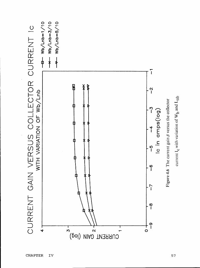
Figure 4.5 Tunneling current component versus doping concentrations ..... 56Figure 4.6 The current gain ß versus the collector
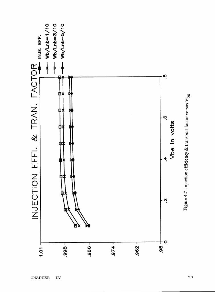
current IC with variation of Wb and Lbb ............................................... 57Figure 4.7 Injection efficiency & transport factor versus VbC ...................... 58Figure 4.8 Transport velocities at b-c heterojunction versus Vbc ................. 59Figure 5.1 A HBT configuration with wide gap emitter
constructed as an "island" ........................................................................ 69Figure 5.2 A HBT structure with a mesa configuration .................................. 70Figure 5.3 An emitter structure with a wide gap base ..................................... 71Figure 5.4 The energy diagram illustrating the blocking of
injection of electrons into wide gap base .............................................. 72Figure 5.5 Inverted collector-up HBT structure .............................................. 73Figure 5.6 A lumped element equivalent circuit of an HBT ........................ 74
III
List of Illustrations and Table viiI
CHAPTER I
Introduction
1.0 Introduction
As a definition, a semiconductor heterojunction is a junction formed by twodifferent dissimilar semiconductors. If the two semiconductors with the Same type ofconductivity (n—n or p—p) are used to form Such a junction, it is called an isotypeheterojunction. If the two semiconductors with different type of conductivity (p—n
or n—p) are used, the junction is called anisotype heterojunction. The introductionof heterojunctions makes it possible to realize electronic devices including highquality lasers [1,2], optical detectors [3], and modulated-doped FETS [4]. The recentbreakthrough in heterojunction applications is the successful realization of highspeed and high gain heterojunction bipolar transistors(HBT).
1.1 An Overview of Heterojunction Bipolar Transistors(HBT)
The introductory concept of heterojunction bipolar transistor is basically awide—gap emitter transistor, originally proposed by Shockley in 1951 [5]. Later,Kroemer analyzed a heterojunction as a wide—gap emitter of a transistor [6].Unfortunately, this device concept did not come into reality until early 70’s becauseof limitations of technology. The emergence of liquid-phase epitaxy (LPE) as atechnology for III-V compound semiconductors resulted in the possibility to bring
heterojunction bipolar transistors into reality. Development of molecular beamepitaxy (MBE) and metal—organic chemical vapor deposition (MOCVD) enabledthe precise control of composition and impurity doping over small distances of the
Chapter I 1 I
order of 50 to 100 A. The above two technologies led to great progress in HBTs.
Currently, lattice—matched material systems mostly used for HBTs are usuallyAluminum Gallium Arsenide(AlGaAs)/Gallium Arsenide(GaAs) and IndiumPhosphide(InP)/Indium Gallium Arsenide (InGaAs). The criterion for a goodmaterial pairs for HBTs application is a close lattice matching. The reason can beattributed to the great concern of the existence of interface states, which result innumerous recombination centers causing a severe degradation in the current gain.For an AlGaAs/GaAs heterojunction, densities of interface states less than 1011 cm'2 can be achieved [7]. However, the density of interface states for an InP/InGaAs ismuch smaller than that for an AlGaAs/GaAs [8].
In conventional homojunction transistors, a tradeoff between the emitter
efficiency and the frequency response exists for consideration of the emitter—basejunction. In order to achieve a significant injection efficiency 1 for an n—p—n
transistor, the hole injection current component Ipc from the base into the emitterneeds to be reduced. This can be achieved by increasing the ratio of the emitterdoping to the base doping. Nevertheess, the emitter doping is limited by the solidsolubility and heavily—doped effects. In addition, the reduction of the base dopingcauses a large base resistance, which degrades the high frequency performance ofthe transistor. In contrast to the homojunction case, the valence band discontinuityAEC for a heterojunction transistor acts as a hole barrier that suppresses the hole
injection. As a result, a high current gain can be obtained without any sacrifice oflow base resistance, Therefore, excellent high frequency performance of HBTsresults in conjunction with good emitter injection efficiency.
Chapter I 2
Advanced technologies, such as MBE and MOCVE, possess the capability ofachieving a base width less than 0.1 pm. The great reduction of the base width leadsto a great reduction of the transit time within the base region. Since the base transittime is a dominant factor limiting the high frequency performance of the transistor, aheterojunction bipolar transistor(HBT) with a thin base can have a high cut—off
frequency exceeding 100 GHz [9]. Numerical simulations suggest a near-ballistictransport when the base region is less than 1000 A and a quasi-electric field of about20 kv/cm exists [10,11]. A ballistic transport means collision—free transit overdistances shorter than a mean free path for the particular electron energy. In HBTs,an important factor to achieve near—ballistic transport is the presence of the "spike",the conduction band discontinuity AEC. This extra potential energy barrier canlaunch the injected electrons into the base region with a substantial kinetic energyand hence with a very high velocity [12].
The "spike" occurs due to the abrupt junction nature. Although the "spike" hassome advantages as mentioned above, there are some drawbacks caused by the"notch", which accompanies the occurrence of the "spike". The "notch" collects
injected electrons and hence enhances the recombination losses. It is desirable toeliminate the notch by growing a graded junction, which yields smoothly andmonotonically varying band edges, thus avoiding the effect. Some researchersexplain that the graded junction possesses an additional advantage over the abruptjunction, a higher ratio of electron to hole current or higher injection efficiency[13].The controversy about the benefit of the graded junction versus the abrupt junction,or vice versa, focuses on the achievement of a large valence band discontinuity AEV.For an AlGaAs material system, the valence band discontinuity, AEV, is quitesmall(AEV = 0.15 AEg). Therefore, the graded junction is usually used in such a
Chapter I 3

material system. However, when the device speed is the main concern, an abruptjunction is often desirable [14]. Actually, the principal benefit of heterojunctiontransistors is not the ability to achieve high current gain, but the flexibility of dopinglevels variations in both the emitter and base regions without any significant sacrificeof injection efficiency, and then to design a well—optimized transistor with consider-ation at a higher performance level [12].
Future potential of HBTs lies in the possibility of incorporating the devicesinto ICs in the near future. Currently, the main interest in HBTs tends to be inhighly integrated digital switching transistors. Such application suggests DoubleHeterojunction Bipolar Transistors (DHBT), meaning a wide—gap collector [12,15].There are several excellent advantages for DHBTs. First, hole injection from thebase into the collector in digital switching applications under conditions of satura-tion can be suppressed. Second, emitter/collector can be interchangeable, by simplychanging the bias conditions, making great improvement on ICs design architectureand high speed switching performance. Moreover, optimization of base and collectorcan be separated. This is especially important in microwave power transistors, inwhich hole mobility is required to be high to achieve low base resistance. For a
microwave power transistor, the transit time through the collector region is dom-inant, as compared to the one through the base. Design of DHBTs can make itpossible to employ a material with high electron mobility, such as InP, as collector toobtain a small transit time through collector. A DHBT made of InP/InGaAs/InPwas reported. Such a transistor exhibits an near-ideal ß versus IC characteristic,
which means current gain independent of the on collector current. Therefore,DHBTs possess a very promising future in high performance transistors and in ICsapplications.
Chapter I 4
The largest benefit, as mentioned above, of HBTs is the ability to have free-dom to select the doping concentration in the emitter and the base regions while areasonably—high current gain can still be achieved. This benefit gives rise tooptimization of the emitter capacitance and the base resistance, which are criticalfactors affecting the upper cutoff frequency and the high speed performance ofmicrowave transistors. It is well known that a junction capacitance of a unsymmetri—cally doped p—n junction depends on the doping level of the lightly doped side.Since the emitter side can be doped less than that of the base side, the emittercapacitance now can rely on the emitter doping level and can be decreased. Also,reduction of the emitter capacitance can improve the noise figure significantly insmall—signal microwave amplification. The most important change made by HBTs
is the great reduction of base resistance due to the highly—doped base. This isbecause both the maximum oscillation frequency fmax for microwave transistors andthe switching time constant for switching transistors are strong function of the baseresistance Rb. Obviously, HBTs are considered excellent candidates for microwaveand high speed switching applications.
Since the advent of HBTs, a lot of efforts have been done on modeling, wherefocus is on the heterointerface and its effects on the transistor behaviors. Difficul-ties of modeling arise from the interface due to the transition between the twomaterials [16]. This transition causes energy discontinuities in both the conductionband and the valence band, producing complicated energy band structure. Also, theeffects of the extra energy potential barriers on the transistor behaviors are of great
concern. The work of modeling HBTs roughly falls into two classes. One class isdirected to model the carrier transport processes within the transistor and to relatethe device’s physical parameters and structural parameters to the terminal parame-
Chapter I 5
I
ters. Another class is pointed at the electrical model represented by lumped
elements using characterization techniques, in which the transistor is considered as a
"black box". It is undoubted that computers and the related software packages playimportant roles in modeling HBTs. So far, no complete model exists that candescribe satisfactorily in describing HBTs. Therefore, investigation of the carrier
transport processes within a typical heterojunction bipolar transistor and construc-tion of an electrical network model through microwave characterization are primary
concerns in this thesis.
1.2 Research Objectives
The main interest in modeling HBTs lies in correctly and accurately describing
the carriers transport mechanisms across the energy barriers caused by the disconti-
nuities. The models for homojunction transistors cannot be directly applied to
HBTs.
« Several models for HBTs have been proposed using similar methods to thoseused in the metal—semiconductor barrier case due to the fact thatmetal—semiconductor structure constitutes a type of heterostructure [17,18]. These
models include the thermionic model, the thermionic—diffusion model, and thethermionic—field— diffusion model for AlGaAs/GaAs HBTs. Researchers have alsoproposed the current balancing concept, where the current transport mechanismacross an interface is treated as two—step process, a thermionic emission process
followed by Schockley diffusion process.Examining the literature research, the following questions need to be
addressed and problems investigated:
Chapter I 6 II
1. Whether the convectional boundary conditions for homojunction transistors
are applicable to HBTs? The referred conditions are usually the equations for theinjected carrier concentrations npb = npo exp(qVb€/kT) and pnb = pm)exp(qVbc/kT), where npo and pm) refer to the equilibrium electron and hole
concentrations, respectively, in the p—region and n—region.2. How should the energy barrier be correctly treated for the conduction
discontinuity?3. How should the conduction band—to—band or direct tunneling be taken into
consideration?4. What are the effects of a short base width and the second "spike" for a
DHBT on the carriers transport process?5. What can be obtained for a InP/InGaAs/InP DHBT if the above consider-
ations are taken?6. Is it possible to propose an electrical network model by using lumped
elements for future characterization?
I Addressing these questions and attempting to answer them consists of theresearch objectives of this thesis. The study in this thesis is basically theoretical.
The main reason for this is due to the lack of facilities for making samples andnonavailability of commercial devices. Therefore, experiments are left to be done infuture.
The thesis consists of five chapters. Chapter I is a general introduction thatoverviews the development of HBTs and outlines the main research objectives.
Chapter II provides the basic theory of heterojunctions. Chapter III introduces thefundamental concepts of Heterojunction Bipolar Transistors. Chapter IV is themain core of the thesis, in which the transport mechanisms are investigated and
Chapter I 7

I
simulated. Chapter V summarizes the main concerns of HBTs in microwaveapplications, Providing a theoretical basis for future work as suggested in thefollowing chapter. Chapter VI is a general conclusion summarizing the mainfindings of the thesis, and directions for future work.
Chapter I 8

I
CHAPTER II
The Basic Theory of Heterojunction
2.0 Introduction
In general, any contact between two different materials in the sense of electri-cal properties consist of a heterojunction. The heterojunctions of most interest arethose between two different semiconductor materials as well as those between ametal and a semiconductor. The concern in this thesis is to thoroughly study theheterojunction between two different III—V compound semiconductor materials.
2.1 Formation of Heterojunction
Conceptually, when two semiconductors with different band gaps and othermaterial parameters are brought into contact, a heterojunction is formed. However,it took almost thirty years to practically and successfully realize this concept. The
successful realization of heterojunctions is attributed to the advances of epitaxialtechnologies, especially MBE and MOCVD. These two technologies are capable of
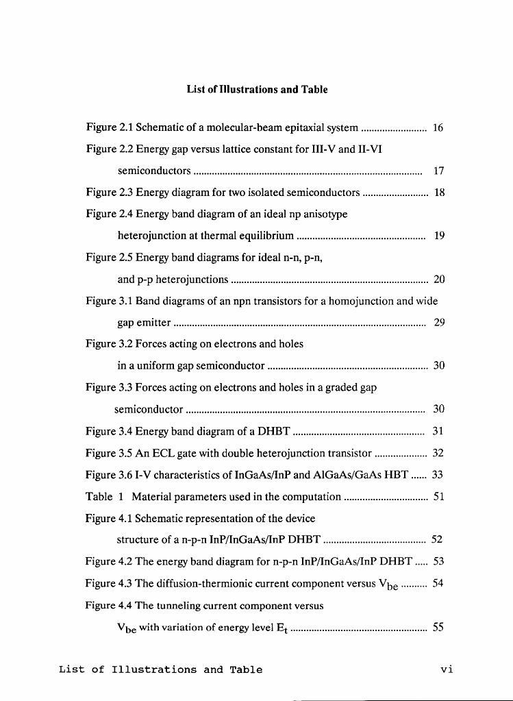
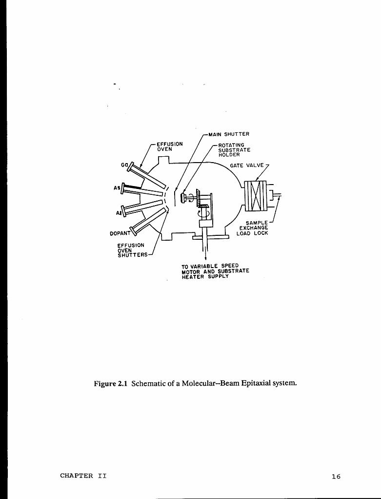
accurately growing and controlling the epitaxial layers and the doping process. Aschematic diagram of the MBE technique is shown in Figure 2.1. Using MBE, alayer of III-—V semiconductor is epitaxially grown on top of different semiconductor
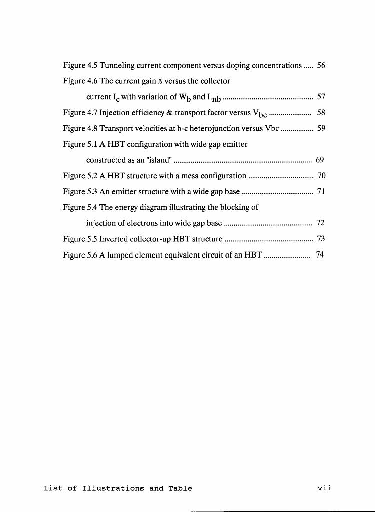
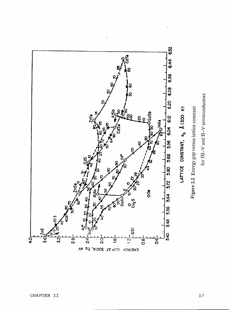
material. A list of various band gaps of III—V semiconductors is given in Figure 2.2
[19]. One can observe that band gaps vary with the variation of compositions of
materials. Therefore, a graded heterojunction is formed if the composition of one ofthe two materials is varied during the growing process. Otherwise, an abrupt
cHAPTER II 9
I
Iheterojunction is achieved. The doping is accomplished at the same time as the Iepitaxial layers growth.
In order to form a high quality heterojunction, the two materials must have asimilar crystal structure and a closely—matched lattice spacing. Two materials withdifferent crystal structures result in crystal dislocations. Mismatched lattice betweentwo materials result in "dangling bonds". These defects become harmful recombina-tion traps, producing undesirable recombination current. Therefore, the selection oflattice—matched material pairs is a very critical factor for successful heterojunctionformation.
2.2 Energy Band Diagram of Typical Heterojunctions[20,21]
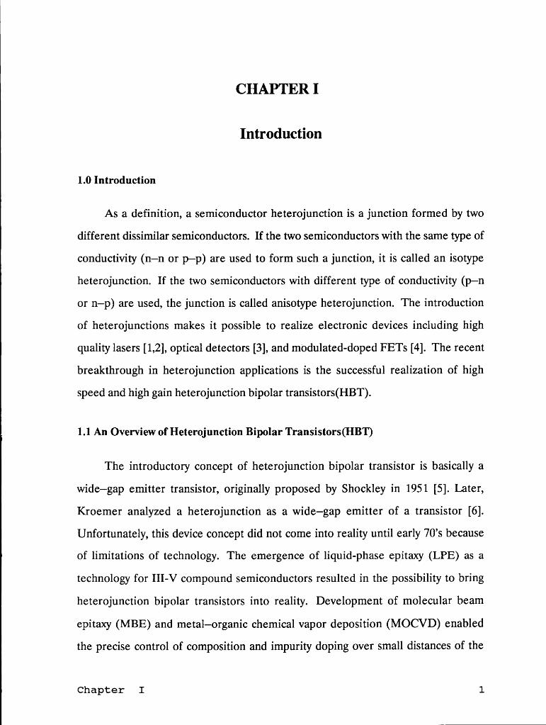
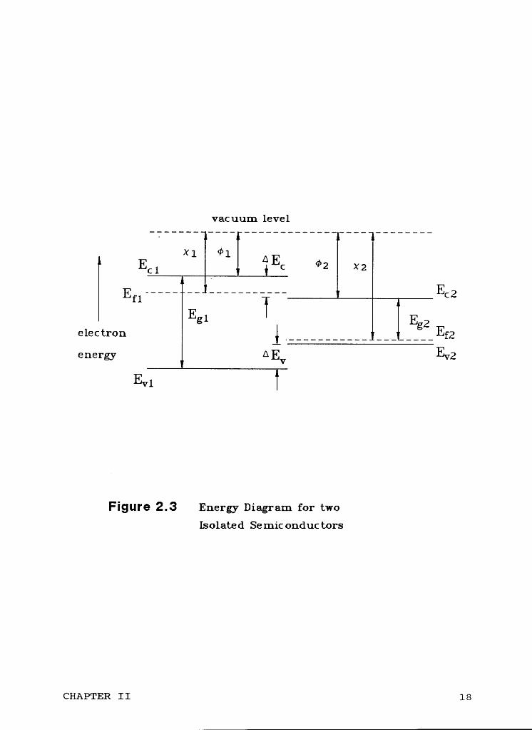
For a typical n—p heterojunction, it is assumed that the two materials havedifferent band gaps Eg, different permittivities 6 , different work functions (pm, anddifferent electron affinities X. When the materials are separated initially, theirenergy band diagram can be illustrated in Figure 2.3. As the case in a homojunction,
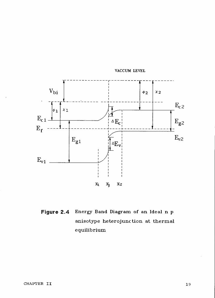
when the separated semiconductors are brought together, their Fermi levels have toline up and the energy band of the transition region is smooth. For a heterojunction,when the requirement of lining—up Fermi levels is satisfied, there have to existdiscontinuities in both the conduction band and the valence band. These discontinu-ities are represented by AEC and AEV, respectively. The resulting energy banddiagram is shown in Figure 2.4. It is noted that this is the case of an abrupt junction.
Since the vacuum level is continuous everywhere and parallel to the band edge, AECis equal to (X 1 - X2) = AX. The related parameters are also shown in the Figure.
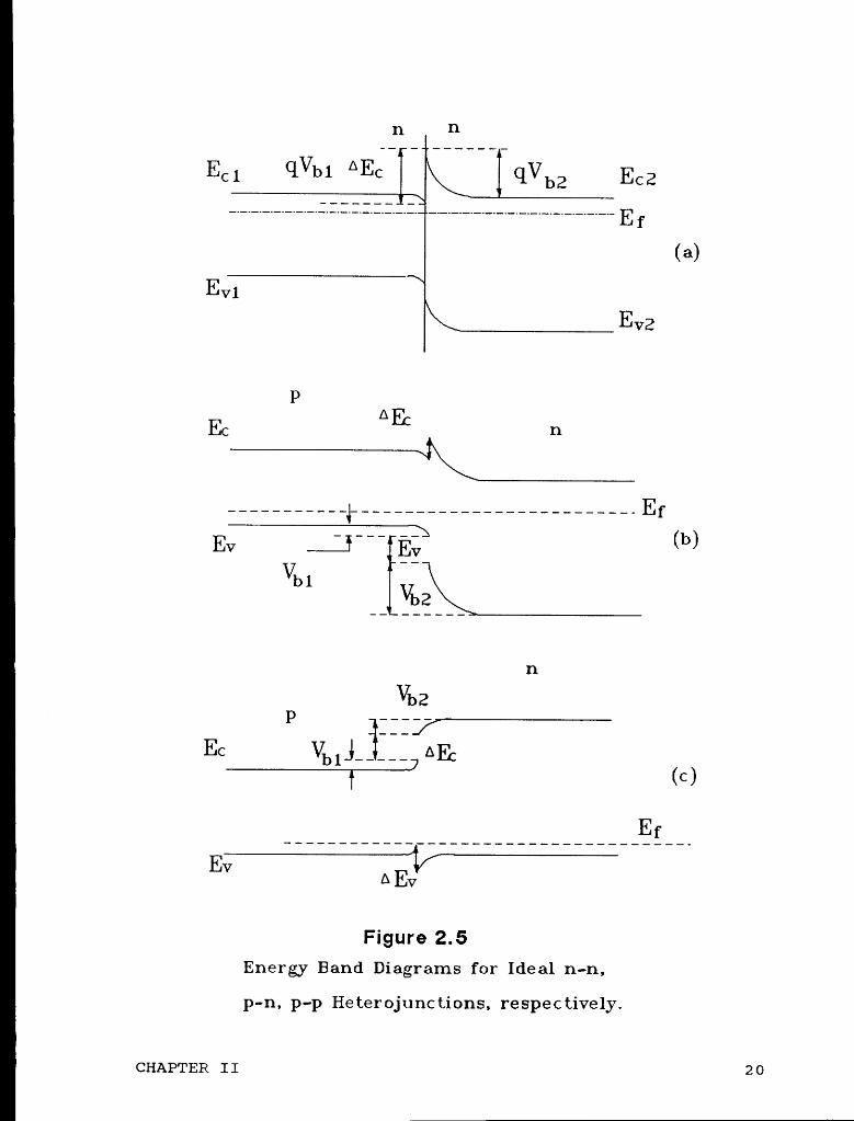
Besides the shown n—p heterojunction, there are three other heterojunctionsI
CHAPTER II 10

r
with different configurations. They are p—n heterojunction, n—n heterojunction, andp—p heterojunction. Their energy band diagrams are shown in Figure 2.5.
2.3 Physical Parameters For A Heterojunction
To describe a heterojunction, the following physical parameters are oftenused:
¢S: work function which is defined as the energy required to remove anelectron from the Fermi level to the vacuum level.
X: electron affinity which is defined as the energy required to remove anelectron the bottom to the vacuum level.
AEC: discontinuity of the conduction band. As an empirical quantity, AEC isCqlläll IOAEC = (X2 - X1) = AX.
AEV: discontinuity of the valence band, which can be given as AEV = (Egl -— AX.
Vbi: The total built—in potential voltage, which is the sum of the partialbuilt—in voltage (Vbil + Vbiz), where Vbiz and Vbiz are the electrostatic potentialsat equilibrium in semiconductor 1 and semiconductor 2, respectively.
•ß(X): potential distribution, which is often obtained by solving Poisson’sequation.
CHAPTER II ll
s (X): electric field distribution, which is also obtained from solving Poisson’sequation.
Aag/ag: relative lattice mismatch rate, where ag is the crystal lattice constant ofsemiconductor material.
2.4 Several Important Formula For p—n Heterojunction [20,21]
The major difference, caused by different material parameters, between ahomojunction and a heterojunction lies in the interface. For each side of a hetero-junction, the equations and methods applied to a homojunction are still applicable tothe heterojunction. Although there are energy discontinuities in the transitionregion, the continuity of electric displacement at the interface holds:
D1 = D2 OI° 61 El = 62 E2 (2-1)
The above equation can be used as one boundary condition for the solution ofPoisson’s equation in order to obtain the depletion widths on each side of theheterojunction:
X1 = (2-2)qND1(‘1ND1 + €2NA2)
and, ·
2NDl€ 16 2 ' V) ä
qNA2(‘1No1 + ‘2NA2)where V is the applied voltage, Ndj and NA2 are the doping concentrations on the
CHAPTER II 12
1
n—side and p—side, respectively. The depletion capacitance is given by:
r NDlNA2‘1€2 äc = (2-4)
2(€lNDl + ‘2NA2)(Vbi - V)
The relative voltage supported in each semiconductor is:
Vbil - V1 NA2€2———- = (2-5)Vbi2 - V2 ND1€1
where V1 + V2 = V, and Vbil and Vbi2 are given by:
Vbi2 = NA2X2/262 (2-7)
It is obvious that the above expressions can be reduced to those for a homo-junction when both material sides are set to be the same.
2.5 Two Important Material Pairs for Heterojunctions
Usually, there are several rules as a guide to select material pairs for hetero-junctions. These rules include a) Select the prime semiconductor of the activeregion with the required consideration of the band-gap and the mobility; b) Selectthe paired semiconductors which possess a very close lattice constant; c) Select thepaired materials which can be fabricated without having technological compatibilityand severe cross—doping problems. Nowadays, there are two important materialpairs for HBTs applications, AlGaAs/GaAs and InGaAs/InP.
From the diagram Figure 2.2, the energy gap versus lattice constant for wide
CHAPTER II 13
range of ternary and binary III—V and II-VI compound semiconductors, one canobserve that GaAs has a lattice constant of 5.653 A with a band-gap of 1.424 ev atroom temperature. Also it is known that AlAs has a very close lattice constant butwith a quite different band-gap of about 2.1 ev. The band-gap of AlGaAs can bechanged, without changing the lattice constant, to obtain a desirable value for HBTsby changing Ga fraction. The electron mobility of GaAs, which serves as the activebase in HBTs, can reach up to 8500 cm2/v—s. In general, AlGaAs is grown on GaAsin order to achieve a good interface. The discontinuity of the valence band AEV isabout 0.44AEg and the discontinuity of the conduction band AEC is about 0.62AEg.AEV and AEC are of great concern in the HBTs design. This point will be discussedin details in the following chapter III. The interface traps, spread over a distance ofabout 140 A on the GaAs side, is about 2 x 1016 cm‘3 and the capture cross section ois 8 x 1015 cm? , implying an interfacial recombination velocity of 104 cm/s[19].
InP has a lattice constant of 5.8686 A with a energy band-gap of 1.35 ev.InXGa1_XAs is found to have a close lattice constant to InP but with a differentband-gap of about 0.75 ev when the fraction factor x = 0.53. In other words,In_53Ga_47As is closely lattice—matched to InP. There are several reasons forselection of this material system. The main reason is that it has an extremely lowbase transit time due to the high electron mobi1ity[22], about 1.1 x 104 cm2/v—s, inInGaAs which is used as the active base. Second, the energy band-gap of InGaAs iscompatible with second generation optical communication system, in which 1.1 —
1.6,um wavelength range is used. Third, InGaAs possesses favorable energy banddiscontinuity: AEC = 0.39AEg and AEV = 0.61AEg [23,24]. Furthermore, Thismaterial system has lower surface recombination(a factor of 100 smaller than
AlGaAs/GaAs system) [8], producing excellent ß —— IC characteristic. Other
CHAPTER II 14
I
properties such as low ohmic contact resistance and excellent interface quality makeInGaAs/InP HBTs a strong competitor to AlGaAs/GaAs HBTs. The main difficul-ties for InGaAs/InP system lie in growing technology: it is difficult to grow P bearingcompounds by MBE and control of p-type dopants by MOCVD [23].
2.6 Conclusion
A heterojunction is formed by two semiconductors which differ in materialand/or conductivity type. The main difference between a heterojunction and ahomojunction in their energy bands is the existence of the conduction band disconti-nuity and the valence band discontinuity in the heterojunction. The primary concernof selection of the materials for heterojunction pair is the lattice matching. A goodheterojunction pair is the one which possesses a very close lattice constant. Themostly common heterojunction pairs are AlGaAs/GaAs and InGaAs/InP.
CHAPTER II 15
wuw suurrsaEFFUS‘°" RomrnweOVEN suesmmeHotoanGo GATE VALVE
As/Ii--innzuI_
DOPANT __ -_-_ 1.0Ao LOCKEFFUSIONOVENSHUTTERS
TO VARIABLE SPEEDMOTOR AND SUBSTRATE
_ HEATER SUPPLY
Figure 2.1 Schematic of a M0lecular—Beam Epitaxial system.
16
l
N_ 885 ··38 3Rz ‘ äS? E ä .„"/ [ 8
B 8 .¤*9•
¢ ° U')Ü:)‘8’J
80 kt äOo¤
V 8F; l
N al g "° Egv -' > Ö cm "‘8 . ,· 56 22
- _ js 2 • ° ' 8 5 *°*"!N0
Q .E:°Ä? cn Lp
. • 383 o?8 ,9 ° gg„ 2 . “8 gä ° Q ° 3· °•• ·— Ü22*;, 6 3 3
3 1% 96* 3 P3 ‘ 9 *3 3 3 "A9 Ö3 °)|OO€ LV ci?9 A9U3N3
1CHAPTER II 17
I
Vacuum level
X1 ¢1Ed AEC ¢2 X2-.... -- ........... Ec2
Egl E 2gelectron l____________ ___ ____Efgenergy AEV Evg
Evl
FÜQLITG 2.3 Energy Diagram for twoIsolated Semic onductors
I
CHAPTER II 18 {,
VACCUM LEVEL
IVb1 I <¢>z X2J I¤ - .... --...--‘.._... .._..I......_... ___ ___
Ec2¢>]_ X1 I IE l I IC
I AE;} Eg2Ef ———— —— -————————-—--I-———4---—-————- -——-— -
I I' EV2Egl I AEVII
{ IEV · I I
I I II I I
I I I
X1 XI X2
Figure 2,4 Energy Band Diagram of an Ideal n p
anisotype heterojunction at thermalequilibrium
CHAPTER II 19
I1 I1
E61 qvbl AEC qVb2 EC2-.-.-.-.-.-.-.-.Ä.I.:.I.I.I.:.-.I. -.-.-....-.-.-.-._.-.-.-.-.-.-._.- E f
(a)Evl
Evi?
P
...........4......................... - EfEv .J Ey (b)
VPI1VbzPE6;
AE(C)
P3L --EV A EV
Figure 2. 5Energy Band Diagrams for Ideal n—n,
p-n, p-p He terojunc tions, respec tively.
CHAPTER II2O
I1
CHAPTER III
Fundamental Concepts ofHeterojunction Bipolar Transistors
3.0 Introduction
In this chapter, the fundamental concepts are to be introduced. As the original
concept, wide-gap emitter transistor is first described. The basic principle of
heterojunction is given to provide the insight of effects caused by the variation of
energy gap on the carrier transport. The effects of the discontinuities in both the
conduction band and the valence band are briefly analyzed. The concept of Double
Heterojunction Bipolar Transistor and the experimental results reported by other
researchers are presented to form the basis of the following chapter.
As an introductory concept, the figure of merit of a bipolar transistor is givenhere:
IC In—II• ICß=“"“"'=l"“"<—_'=ßmax (3'ZI-)
Ib Ip+II.+IS Ip
where ßmax is the possible maximum current gain of a transistor, Ib and Ib are the
collector and base currents, respectively, In and Ib represent the electron currentand hole current components injected across the emitter junction, respectively, and
II and IS are the recombination currents within the base region and the space Chargeregion, respectively, In has to increase and/or Ip has to decrease in order to achievea large current gain. The desire towards the possible maximum current gain ßmax
CHAPTER III 2 1
leads to the concept of the wide gap emitter.
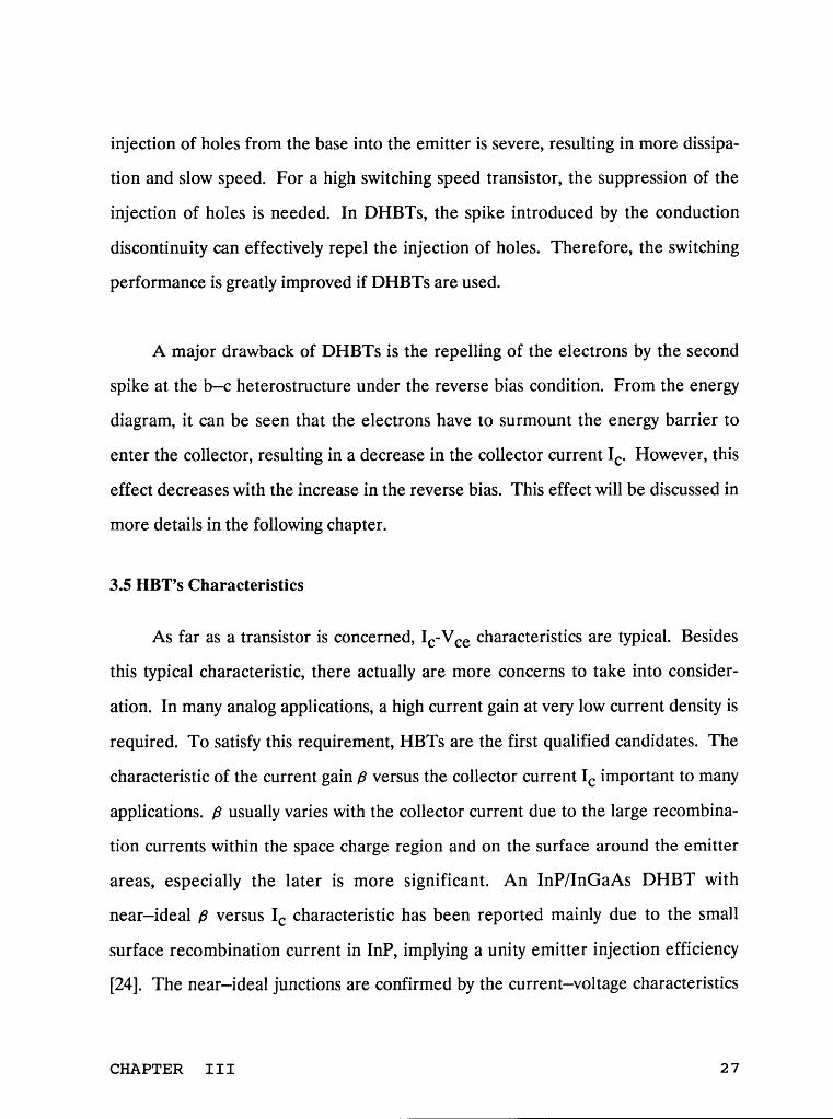
3.1 Wide—gap Emitter Transistor Concept
The energy diagrams for a homojunction and a heterojunction are drawn inFigure 3.1. For a homojunction, the energy barrier, denoted qVn, for holes injectedfrom the base into the emitter is the same as the energy barrier, denoted qVn, for
electrons injected from the emitter into the base. Then the current In and In can beexpressed as:
In = qvnbNDeexp(-qVn/kT) (3-2)
and
In = qvneNAbexp(—qVn/kT) (3-3)
where Vub and vpn are the mean speeds of electrons at the emitter—end of the baseand of holes at the base—end of the emitter, respectively, and NDB and NAb are thedoping concentrations in the emitter and the base, respectively. The ratio of In/In
can be obtained. The ratio is proportional to the ratios of the mean speeds vnb/vncand the doping levels NDC/NA},. Usually, vnb/vnc is between 5 and 50. Therefore,the doping ratio NDC/NAb is required to be at least 102 in order to obtain a usefulcurrent gain(e.g. >100). The dependence of the current gain on the doping ratiogives rise to some difficulties to optimize a homojunction transistor. For example,high frequency performance, in turn, low base resistance requires high doping level
in the base while high current gain requires low doping level in the base. A possible
way to overcome these difficulties is to increase the hole barrier such that the hole
current component is much less than the electron current component. This idea can
be accomplished by using a wide—gap material for the emitter, implying a hetero-
CHAPTER III 22
1
junction structure.
For a wide—gap emitter heterojunction transistor, the energy barrier holes is atleast a few kT larger than the barrier for electrons. The difference between the twobarriers is given by:
(qVn - qVp) = AEg - AEb ~ AEV (3-4)
Now, the maximum current gain ßmax is given by [12]:
Vnb NDeßmax = i ———— exp (AEV/kT) (3-5)
Vpe NAb
Suppose AEV = 0.61AEg = 0.36 ev(this is the case in InGaAs/InP in which AEg =0.6 ev). Then, exp(AEV/kT) is a factor of 106, which is much larger than the mean
speed ratio and the doping level ratio. In other words, the maximum current gain is
almost only dependent on the valence band discontinuity AEV.
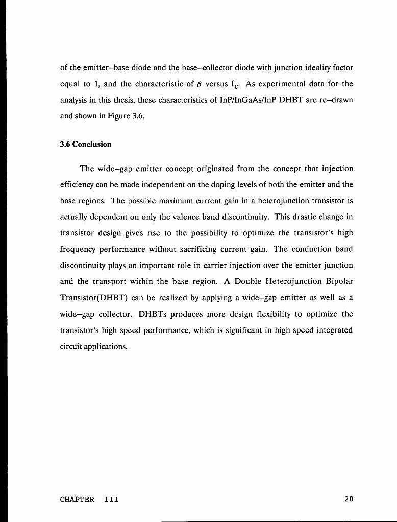
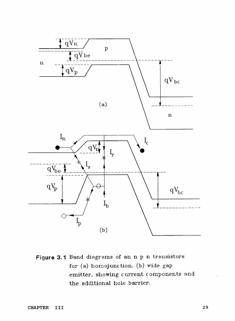
3.2 A Basic Principle of Heterojunction [12]
A basic principle as a guidance in design and development of heterojunction
devices simply means that variation of energy gap, resulting in a force acting oncarriers, is utilized to control their flows and distributions. This principle can beunderstood by observing the forces acting on both electrons and holes within a
heterojunction device. The forces acting on electrons and holes are equal(but the
signs are opposite to each other) to the slopes of the edge of the bands. In a homo-
junction, the slopes are supposed to be constant due to the constant energy gap.
Therefore, two forces, acting on electrons and holes, are also supposed to be equal
CHAPTER III 23
in magnitude and opposite in sign, as shown in Figure 3.2. However, the force actingon electrons is different from that acting on holes in a heterostructure due to thedifferent slopes resulting from the variation of the energy bands, as shown in Figure3.3.
For example, the idea of the wide-gap emitter originated from the intentionthat a larger force is added to the holes injected from the base into the emitter thanthe one to the electrons injected from the emitter into the base. As a result, the ratioof the electron current to the hole current In/Ip is increased by the difference,instead of by the difference between the doping levels, between the two actingforces, produced by the different slopes in the conduction band and the valenceband. The "spike" at the conduction band is found to have two—fold functions. Onone hand, the height of the spike may produce a near ballistic transport through thebase, resulting in a high speed. On the other hand, the existence of the spike repelsthe injection of electrons into the base, leading to a decrease in the ratio IH/Ip, inturn a decrease in the current gain ß. Therefore, an optimum height of the spike isdesigned to make a compromise according to the device’s main requirements.
3.3 Effects of Discontinuities
In fact, the drastic changes caused by HBTs result from the discontinuity of thevalence band. The effect of AEV on the current transport can quantitively beexpressed by equation (3-5). The physical explanation for this is given in theprevious section. Apparently, the possible maximum current gain is uniquelydetermined by the value of the discontinuity and a very large current gain is abso-
CHAPTER III 24
1
lutely obtainable. Unfortunately, a large value of AEV is not easily achieved. It isaffected by the growing processes. The reported values of AEV are good enough to
produce successful HBTs.
A brief description of the two—fold functions of the "spike" has been given inthe section 3.2. The "spike" results from the conduction band discontinuity AEC.This potential spike project above the conduction band of the narrow gap base,causing a net energy barrier for the injection of electrons from the emitter into thebase. If the effect of the carrier transport within the base on the injection is tempor-
ally neglected, an extra emitter—base voltage in the order of AE},/q is required toproduce a given electron current density. In other words, the existence of the spikereduces the current ratio In/Ip by a factor of exp(-AEb/kT). However, the injectionof electrons into the base is actually affected by the distribution of the electrons
within the base. The extra potential spike may inject the electrons into the base witha substantial kinetic energy such that the electrons move through the base regionwith a very high velocity(«, 108 cm/s). Since in III—V compound semiconductors, the
dominant scattering mechanism is the polar optical scattering, which is directionaldependent, the electrons possess the high forward velocity for several collisions. Asa result, a near—ballistic electron transport through the thin base is produced. Such anear—ballistic transport possesses a significant effect on the device speed and thedevice current gain. It is necessarily noted that an over—high "spike" may result inslow transport velocity because the electrons with high energy will transfer to the
next energy valley where the electrons have low mobility. Therefore, the height of
the spike needs to be carefully chosen and controlled.
When the spikes, existing at both e-b junction and b—c junction for DHBTs,
CHAPTER III 25
become too thin due to the applied voltages, the electrons may tunnel through thespikes. Multi-transport mechanisms have to be considered at the e—b junction sincethe upper portion of the spike is thin enough to cause the electron tunneling.Tunneling also possibly happens at the b-c junction because of the thin spike causedby the reverse bias. Furthermore, the spike at the b-c junction has repelling effecton the approaching electrons.
3.4 Double Heterojunction Concept [12,15,23]
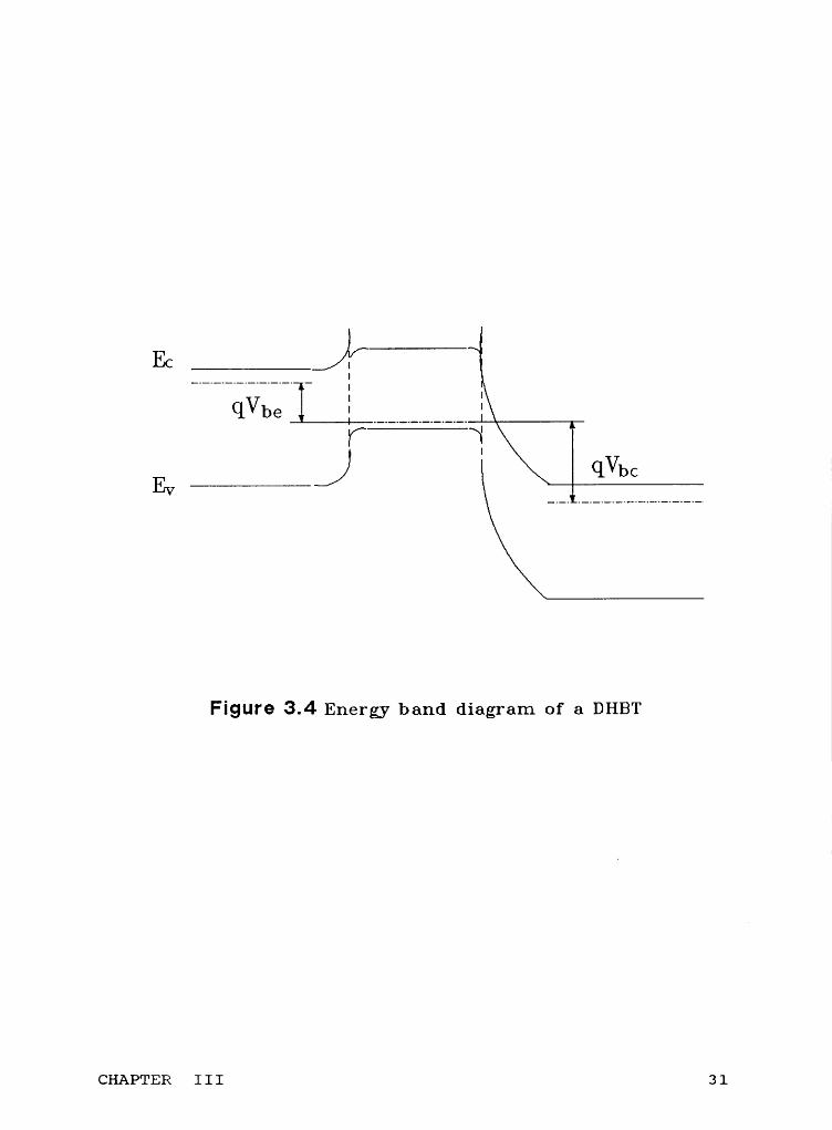
A Double Heterojunction Bipolar Transistor(DUBT) is the one with
wide—gap emitter and wide—gap collector. Its energy diagram is shown in Figure 3.4.Like the use of a wide—gap emitter, the use of a wide—gap collector gives the
possibility to optimize the transistor’s performances and more design flexibility.
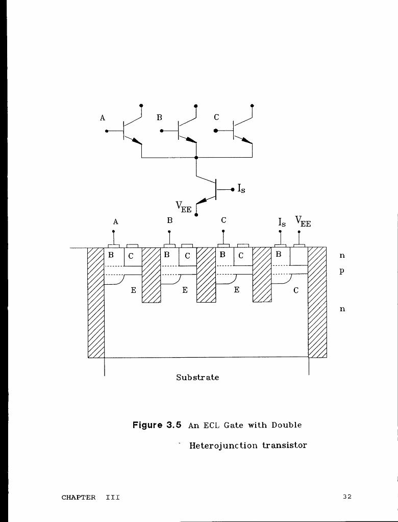
The interchangability between the emitter and the collector is the mostimportant advantage of a DHBT. The performance of the transistor remains thesame with the emitter up or down. In other words, The roles of the emitter and thecollector can be substituted for each other simply by changing the bias conditions.This feature is significant for highly integrated circuits. For example, an ECL gatehas four transistors. The emitters of three transistors are connected to the collectorof the fourth. These four transistors can be easily realized by using DHBTs withcollector—top configuration within the same insulating island, as illustrated in Figure
3.5.
In the switching digital circuit, the collector is often driven into saturation.Usually, the base region is more heavily doped than the collector. In this case, the ,
11
CHAPTER III 26 I
II
injection of holes from the base into the emitter is severe, resulting in more dissipa-tion and slow speed. For a high switching speed transistor, the suppression of theinjection of holes is needed. In DHBTs, the spike introduced by the conductiondiscontinuity can effectively repel the injection of holes. Therefore, the switchingperformance is greatly improved if DHBTs are used.
A major drawback of DHBTs is the repelling of the electrons by the secondspike at the b—c heterostructure under the reverse bias condition. From the energydiagram, it can be seen that the electrons have to surmount the energy barrier toenter the collector, resulting in a decrease in the collector current IC. However, thiseffect decreases with the increase in the reverse bias. This effect will be discussed inmore details in the following chapter.
3.5 HBT’s Characteristics
As far as a transistor is concerned, IC-VCC characteristics are typical. Besidesthis typical characteristic, there actually are more concerns to take into consider-ation. In many analog applications, a high current gain at very low current density isrequired. To satisfy this requirement, HBTs are the first qualified candidates. Thecharacteristic of the current gain ß versus the collector current IC important to many
applications. ß usually varies with the collector current due to the large recombina-tion currents within the space charge region and on the surface around the emitter
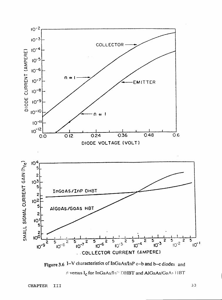
areas, especially the later is more significant. An InP/InGaAs DHBT withnear—ideal ,6 versus IC characteristic has been reported mainly due to the smallsurface recombination current in InP, implying a unity emitter injection efficiency[24]. The near—ideal junctions are confirmed by the current—voltage characteristics
CHAPTER III 27
ZI
of the emitter—base diode and the base—collector diode with junction ideality factor i
equal to 1, and the characteristic of ß versus IC. As experimental data for theanalysis in this thesis, these characteristics of InP/InGaAs/InP DHBT are re—drawnand shown in Figure 3.6.
3.6 Conclusion
The wide—gap emitter concept originated from the concept that injectionefficiency can be made independent on the doping levels of both the emitter and thebase regions. The possible maximum current gain in a heterojunction transistor isactually dependent on only the valence band discontinuity. This drastic change intransistor design gives rise to the possibility to optimize the transistor’s highfrequency performance without sacrificing current gain. The conduction banddiscontinuity plays an important role in carrier injection over the emitter junctionand the transport within the base region. A Double Heterojunction BipolarTransistor(DHBT) can be realized by applying a wide—gap emitter as well as awide—gap collector. DHBTs produces more design flexibility to optimize thetransistor’s high speed performance, which is significant in high speed integratedcircuit applications.
CHAPTER III 28
--.-.-.-.-.-.-.-.-. -.-.-.- PqVbe
Iqvp /qvbc
(a) .-.-. .-.-.-„-.-.-.-.-.-.-Il
CqV lr ,-.......-.-.-....-.-....- ...- Iqvbe gw- -....-.- ..1-.-.-. .-.„.-.-.-.-.-....-.-.- .-.-.-.-. .-.-
qVP qvbc
° lpCb)
Figure 3,1 Band diagrams of an n p n transistorsfor (a) homojunction. (b) wide gapemitter, showing current components and _the additional hole barrier.
cHApmER III 29
ÄFigure 3.2 Forces acting on electrons and holes
in a uniform gap semiconductor
Figure 3.3 Forces acting on electrons and holes
in a graded gap semiconductor
ÄcHA1>1—ER III 30 ;e
I
I-.-.-._.-.-.-.-.-. - •
qvbeV
IEV
qvbc
Figure 3.4 Energy band diagram of a DHBT
CHAPTER III 31
B
B
IO°2IO'}
COLLECTOR——-—•·ui IOEJ -5
In_ IOEV |O·6
11 ¤= I·————•
E 10°7cx3 10°°ä 10°95 IO°IO
10"'0.0 012 0.24 0.36 0.48 0.6
OIOOE VOLTAGE (\/01.T)
’}_• IO4E 5
E 2<¤ IÜ31- 5pi, 2 InGOAs/InPOHBTä
IO2_, 5 AIGGAS/GQAS HBT< 2ä 1gu IOSQ 2 . _ .äIOO23I252525I25 2525 zsi
lO°9 IO. 6 IO°7 IO°6 IO- 5 IO.4 IO'} IO- 2 IO.. JCGLLECTOR CURRENT (AMPERE)
Figure 3_6 1-V charactcristics of InGaAs/InP e—b and b—c diodes andH versus IC for InGaAs/I11*’ DHBT and AlGaAs/Ga/\s { {BT
cHA1>TER III 33 II
CHAPTER IV
Theoretical Investigation of TransportMechanisms For n—p—n InP/InGaAs DHBT
4.0 Introduction
The concerned transport process of injected carriers is accounted for from the
edge of the e-b depletion on the emitter side to the edge of the b-c depletion on the
collector side. The process consists of the injection of carriers over the e-b junction,
the transport through the base, and the collection by the collector. Three theories
are used to describe the whole transport process; thermionic emission, drift-
diffusion, and tunneling. To order to obtain an accurate current device model, the
three current transport mechanisms are applied and the proper boundary conditions
are selected, based on the physical considerations, at different boundaries.
InP/InGaAs material system has been proved to be a very promising pair forhigh frequency transistor applications. The model is applied to a Double Hetero-junction Bipolar transistor. Therefore, the investigation of the current transport
processes, discussed in this chapter, is applied to an n—p—n DHBT made from
InP/InGaAs/InP.
4.1 Device Physical Structure [25]
The schematic representation of the device structure is illustrated in Figure
4.1. The device can be etched to a mesa configuration to reduce the surfacerecom-binationcurrent. A buffer layer is inserted between the InP substrate and the
CHAPTER IV 34
1
collector layer. The InP collector region is n—type doped with a concentration equalto 1x1017 cm'3 with a thickness of 0.5 pm. The InGaAs p—type base layer is doped
to 2x1018 cm‘3 with a thickness of 0.1 pm. The InP emitter layer is then grown ontop of the base and doped to 2x1017 cm'3 with a thickness of 0.3 pm. Another layer
of heavily—doped InGaAs is formed on top of the InP emitter for metallizationcontact. The band—gap for InP is 1.35 ev and for InGaAs is 0.75 ev. Therefore, this
is a wide—gap emitter and wide—gap collector double heterojunction transistor.
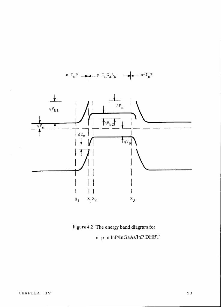
The energy band diagram for the device is illustrated in Figure 4.2. An abruptheterojunction approximation is taken into consideration. When the biases are
applied to the two interfaces, the energy band of the emitter is raised and the energy
band of the collector is lowered with respect to the neutral base region. The changesof the energy bands as the biases change are good demonstrations of physicalphenomena inside the device, leading to an understanding of carrier transportprocesses.
4.2 Current Gain ß and the Concerned Current Components
The current gain ß of the transistor is a good figure of merit to evaluate theperformance of the transistor when the description of the carriers transport processis considered. ß is given by:
ß = T QT (4-1)
where T is the injection efficiency of the emitter and GT is the base transport factor.
When the voltages Vbc and Vbc are applied to the e-b junction and c-b
CHAPTER IV 35 {
l
junction, respectively, the four current components, Jn, Jr), JS, and Jr are included in
the whole current transport starting from the edge of the depletion region of the e-bjunction on the emitter side, xl, to the edge of the depletion region of the c-bjunction on the base side, x3. JH is the electron current density injected from the
emitter into the base, Jr) is the hole current density injected from the base into the
emitter, JS is the sum of the electron-hole current density due to the generation-recombination within the forward-bias emitter-base depletion region and the surface
recombination, and finally Jr is the electron current density of bulk recombinationwithin the base region.
When these four current components are considered, ·r, cz-l-, and ß can be
expressed in the forms,
InT = —————————————— (4-2a)
In + In + IS
In - IS - IrGT = ··—···——·——· (4*21))
In - ISand
IC In — Ir.ß = --—— = —-—-————————— (4-2C)
Ib In + lr + IS
where IC and Ib are the collector terminal current and the base terminal current,respectively.
4.3 Electron Injection Current at e-b Heterojunction (Jrr)
For the drift-diffusion current mechanism, the transport current isdescribedCHAPTER
IV 36
I
by the Boltzmann transport equation of the form,
Jp = q ßn ¤ v¢„ (4-3)
where 4>H is the electron quasi-Fermi level (imref), n refers to the electron concen-
tration, and pn is the electron mobility. In the transport equation, two kinds of
driving forces associated with electron motion are included; the first force is the
imref gradient and the second one is the field. These two forces exist withinX1 <x<xj without considering the potential energy maximum. When one considersa case where the potential energy barrier is so sharp that electrons one mean free
path away from the maximum can gain or lose kinetic energy 2kT, one encounters a
serious problem in applying the Boltzmann transport equation properly. The
problem is that the field component to the current at the potential energy maximum
does not exist anymore. The solution to this problem proposes the use of the ther-
mionic emission [26]. Such a case exists at an abrupt heterojunction due to the
conduction band discontinuity AEC at the interface. Therefore, diffusion combined
with thermionic emission is considered to treat the electron injection over the energybarrier at the e-b junction.
The basic concept in that solution is that the drift-diffusion is applied within X1
< x < xj, while the thermionic emission theory is used at the potential energy
maximum, actually right at the boundary or the interface.
From equation (4-2), one can obtain,
Jr) = q)ur1Nc €Xp["q('ß(x) ' ¢n(X))/kT] V¢n (4-4)
CHAPTER IV 37
where NC refers to the state density of InP and ¢(X) is the potential distributionwithin the depletion region. The above equation is integrated between the limitsX1 and xj, one can obtain,
J¤ X 4* (X) d¢„ (4-5)q ßn Nc X1 ¢n(x1)
If one defines the edge of the depletion region as the reference, equation (4-5)can be obtained,
¢(xl) = ¢n(xl) = O (4*5)
selecting the proper reference and assuming a constant doping concentration, one
can obtain from Poisson’s equation an expression of the potential distribution of theform,
¢(X) = -qND€(x2+xlx)/26l+(1+x/xl)(Vbil—Vl) (4-6)
where Vbil and Vl are the built-in voltage drop and the applied voltage drop,respectively, on the emitter side. Substituting equation (4-6) into (4-4), one can
obtain,
._. q Ld V1 2J2¤ q Dn NC NDC @xp[———————] (exp(q¢C(X)/kT) - ll2 X1 kT
JI1 (X ) = 4 **7 )F021[(X*km)/Ld] * FO21['(X1+km)/Ld]
where Ld is the Debye screen length for an electron concentration equal to the
CHAPTER IV 38
acceptor doping concentration. Ld is of the form,
E 1 k TLC >1/2 <4-vb>q NDe
F0,1(x) is the normal distribution function. km is a factor of the form,
E1 V1km ¤ - —-——-— (4-7C)
q NDeX1
Considering thermal emission at the potential energy maximum, one can have
[20],
Jn = q Vth [ nm(xj) ' nO(xj)] (4'8)
where vm is the thermal velocity given by equation (4-9),
Vth = A* T2/q NC (4-9)
nm(Xj) is the electron density at xj when the current is flowing, n0(Xj) is a quasi-equilibrium electron density at xj, and A* is the effective Richardson constant.
The electron densities Hm(Xj) and n0(Xj) are given by,
nmxj) = NC expt - ——-—————- J (4-10a)kT [
CHAPTER IV 39[

[
and
qVbi1°qVlH0(Xj) = NC eXp[ — —————————— ] (4-lOb)
kT
Equating equations (4-7), (4-8), and (4-10), one can obtain the expression for
electron injection current Jd_t at xj
q vth NC exp(—qVbil/kT)[exp(qVl/kT) — 1](4*11)
1 +Vth{FO'l[(X'km)/Ld] * FO’1[-(X1-km)/Ldl}
]2nIn
addition to the diffusion and the thermionic emission mechanisms, it is
possible for electrons to tunnel through the energy barrier due to the energy-band
structure. From Figure 4.2, it can be seen that part of the "spike" at the e-b hetero-
junction is above the conduction band of the base. This portion increases as the
applied voltage increases. In other words, those electrons on the emitter side with
energy less than the height of the "spike", Eb, but larger than the energy level of thebase conduction band, may form a current by tunneling through the "spike". In fact,this is the case where tunneling occurs from one conduction band into another
conduction band. To evaluate the tunneling current Jam, one can have [27,28],
41rqm*Jtun = f <1E(Fe(E) * Fb(E) )f P(Ex) <1Ex (4*12)
where EX is the electron energy in the tunneling direction, F€(E) and Fb(E) are the
Fermi-Dirac distribution functions in the emitter conduction region and the baseconduction region, respectively, and P(Ex) is the tunneling probability given by,
CHAPTER IV 40
ln P(Ex) = - Q f( ¢(x) - Ex )l/2 dx (4-13)
Q - 2 (2m*)1/2/h
It is very difficult to obtain an accurate analytical expression for P(EX) fromequation (4-13) for the given potential expression 1/>(X). However, equation (4-13)can be evaluated by expanding it with respect to a carefully—chosen energy level Et.By selecting a certain Et means that electrons with energy close to Et have largetunneling probability. Then, P(EX) can be expressed as
ln P(EX) = * [ ä + b(Et * EX) + •••] (4-14)
X 2where, a = Q I [¢(x) - Et]l/2 dx
X11xlz -1/2b = 1/2 Q f [¢(X)
— Et] dxX11
and (xll — xlz) is the tunneling length.
4.4 The Recombination current In The Base Region (Jr)
The injected carriers from the emitter into the base are considered to diffusethrough the neutral base region. The bulk recombination current forms during thediffusion. According to the diffusion theory, the diffusion current can be deter-mined as long as the excess electron distribution is obtained. The magnitude of the
recombination current is equal to the subtraction of two currents JH(x2) and Jn(x3)at the two boundaries of the base, respectively.
In order to obtain the excess electron distribution Anp(x) within the base
CHAPTER IV 41
11
region, the continuity equation is solved in the one-dimensional case under steady-
state conditions,
d2Anp (x) Anp(x)DI-lb —————— •' ————————· = O (4-].5)
dX2 'T nb
where Dnb and rnb are the electron diffusion coefficient and the electron lifetimein the base region, respectively.
As seen from the energy band diagram, the "spike" due to the conduction band
discontinuity plays an important role in affecting further transport of injected
electrons after crossing it. In fact, the "spike" may inject the electrons into the base
region with a substantial kinetic energy, and hence with a very high velocity [12].
The kinetic energy results from the transformation of the potential energy concern-
ing the height of the spike. Estimation of the electron velocity when electrons "fall"
down from the top of the spike may be made using a simple expression of the form,
1/2 m* v2(x) = AEC (4-16)
and,
AEC = AEC — q( Vbiz - V2 ) (4-17)
where v is the initial velocity with which electrons move away from the interface, m*
is the electron effective mass, AEC is the conduction band discontinuity, AEH is the
potential energy of the spike, Vbi2 and V2 are the built-in voltage drop and theapplied voltage drop on the base side. Since all the injected electrons move initially
with high velocity in a positive direction away from the interface, the BoltzmannStatistics, requiring the random distribution of the velocity, is not satisfied[28]. Only
CHAPTER IV 42
when the injected electrons experience several periods of scattering, the traditionaldiffusion equation can be applied. Usually, the mean free path of an electron
between collisions is of the order of 102 A. The calculated value of the width of the
depletion region on the base side is less than 10‘6 cm. Thus, one can reasonably
assume that the injected electrons reach the edge of the neutral base region almost
without loss. In other words, the concentration of the excess electrons which begin
to diffuse at x = X2 across the base region is the same as the amount of the injectedelectrons at x = xj. According to the above statement, the excess electron concentra-
tion is given by,
A¤p(x2> = J„(xj>/tq v(xj>3 (4-l8¤>
The influence of the excess electron level by the e-b junction applied voltage Vbc is
through JH for V1 and v for V2.
Taking the effect of the spike at b-c junction into consideration (will be
discussed in the next section), one can find the boundary condition at x=x3 of the
form,
Anp(x3) = Jn(X3)/qVt (4-18b)
where vt is the transport velocity at the boundary x = x3.
Based on the two boundary conditions, equations (4-18a) and (4-18b), the
excess carrier distribution is obtained,
CHAPTER IV 43
1 Wb'XAnp(x)=j-————-——[Anp(x2)sinh(———)+Ar1p(x3)sinh(x/Lub)] (4-19)
SlHh(Wb/Lnb) Lnb
Then, an expression for Jr can be derived as,
q Dub Anp(x2) cosh(Wb/Lub) 1(
B= -———————[-————-— — —— —————————)
Lnb SiHh(Wb/Lnb) A SiDh2(Wb/Lnb)
1* ———·**——·— ] (4*20)
A Sihh(Wb/Lnb
where,
COSh(Wb/Lnb)A = B ———-———————— + 1
SiHh(Wb/Lnb)
DnbB = ...l....
Vt Lnb
Lub = (Dub rub )1/2 is the electron diffusion length, rub and Dub are the electronlifetime and the electron diffusion coefficient, respectively, within the base region.
4.5 Effect of the b—c Barrier on the Transport Process
The injected electrons encounter the second spike at the b—c junction. It is
assumed that they reach that boundary, x=x3, with the thermal Velocity Vrb/4 [29].
Two possibilities exist for them to cross this barrier into the collector region; one is
that the electrons penetrate through the barrier by tunneling. This case occurs
usually with a low reverse bias at which the barrier is high but thin. When a high
CHAPTER IV 44
reverse bias is applied so that the height of the barrier decreases further more andeven disappears, the thermal emission of the carriers across the barrier can bepossible. The electron blocking action of the spike causes the injected electrons tobe accumulated more and consequently more recombination is expected. This leadsto a decrease in ß and dependence on VOO as well. The effect of the spike on theelectron transport can be described in terms of a transport velocity vt, which is anexponential factor less than the thermal velocity vth/4. For the tunneling case[30],
vt = vth/4 exp[—2(2m*/n2)l/2 AEOl/2 d] (4-21)
For the thermal emission case, vt may be written as,
Vth AECvt = —— exp(- —-—) (4-22)
4 kT
where h is the reduced Plank’s constant, d is the thickness through which theelectrons tumiel, and ABO is the height of the barrier given by,
AEC = AEC - q(Vbi2 - V’2) (4-23)
V’2 is the voltage drop of the applied bias at the base region side. It is noticed that asimplified expression for tunneling current, instead of equation (4-12), is used due to
the reverse-biased junction. Obviously, vt is a function of VOO since the features ofthe energy barrier is determined by Vbc.
4.6. The Recombination Current In Depletion Region (JS)
An expression for the bulk recombination current Irgb for the heterojunction
CHAPTER IV 45
I
under consideration is derived as,
X1 X2Jrglb = q 3 [ U1 dx + [ U2 dx 3 (4-24)
O O
where U1 and U2 are the recombination rates within X1 and x2, respectively. U1 andU2 are given by,
U1 Ol Vthl Nt]- Dil (4*25)
U2 = (1/2) 02 vtH2 Nt2 n12 (4-26)
where 01, 02, Vth1,Vth2, N11, Ntz, n11, and H12 are defined in the Table 1.
On the other hand, the surface recombination current is given by,
IHSIS = (1/2) q n12 so AS exp(qVbS/2kT) (4-27)
where s0 is the surface recombination velocity, AS is the base surface area whererecombination occurs. so is of the form,
so = 02 Vthz ( n k T DSt ) (4-28)
Thus, JS can be represented as,
JS = Jrglb + JHSIS (4-29)
4.7. Hole Injection Current at e-b Heterojunction (JH)
It is known that the hole current component is greatly suppressed by the
valence band discontinuity AEV. The ratio of the electron injection current JH to the
CHAPTER IV 4 6

hole injection current Jb is approximately evaluated by equation (3-1), rewritten as, F
Jn/Jp = ßmax = A exp(AEV/kT) (4-30)
where A is a constant and AES, is the valence band discontinuity between InP and
InGaAs. Since AES, is about ten times of kT for the material system considered, theratio is at least larger than 103. Practically, Jb is much less than the recombination
current JS, or Jb< < JS. This simply means that the hole current component Jb
becomes negligible compared to the recombination current. Therefore, it is notnecessary to evaluate Jb in detail in this study.
4.8 Simulation Results and Analysis
Computations of these current components are based on the material parame-
ters recently reported for InGaAs and InP in the literature and structural parameters
of the device shown in Figure 4.1. The material parameters are given in Table 1.
The diffusion-thermionic emission and the tunneling current components are
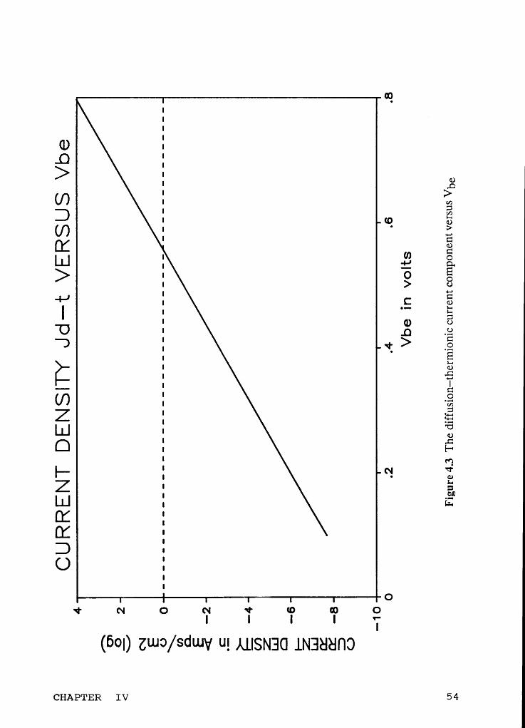
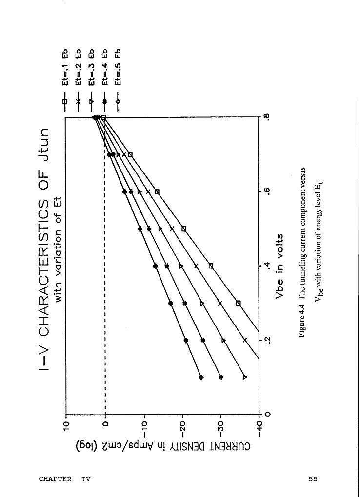
evaluated first. The result of Jd_t is presented in Figure 4.3. The current densityvalue at Vbb = .8 v is about 104 amps./cm2. Different values of Et, which are 0 <Et < Eb, are used to compute the tunneling currents Jum. The results are shown inFigure 4.4, indicating that Et = .5 Eb possesses the largest tunneling probabilityvalue. Comparing the results of Figure 4.3 and Figure 4.4, one can find that the
diffusion-thermiouic emission current dominates over the tunneling current compo-
nent by a factor of 102. The reason can be mainly attributed to the barrier’s thick-
ness. As known, the tunneling current is quite sensitive to the energy barrier’s
thickness. A thickness of the energy barrier for a doping concentration of 2 x10¹⁷/cm3 is about 500 A, which is not thin enough to cause a significant tunneling
CHAPTER IV 47
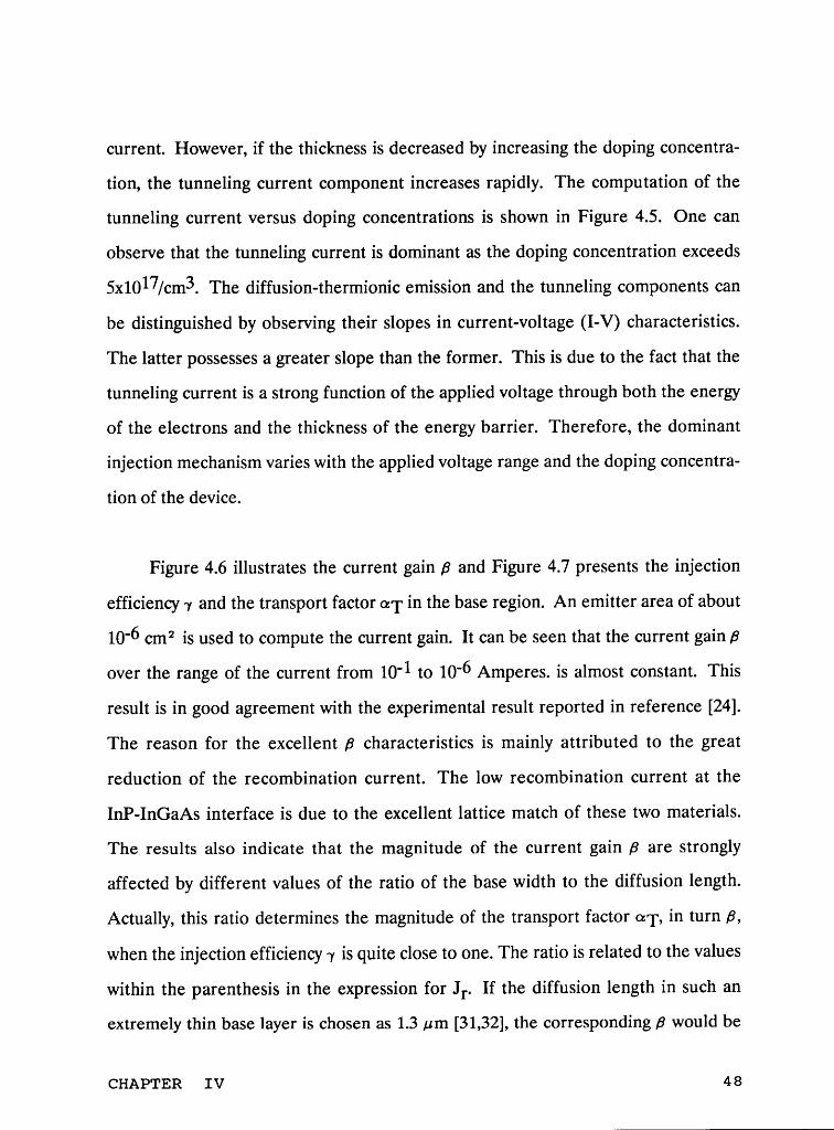
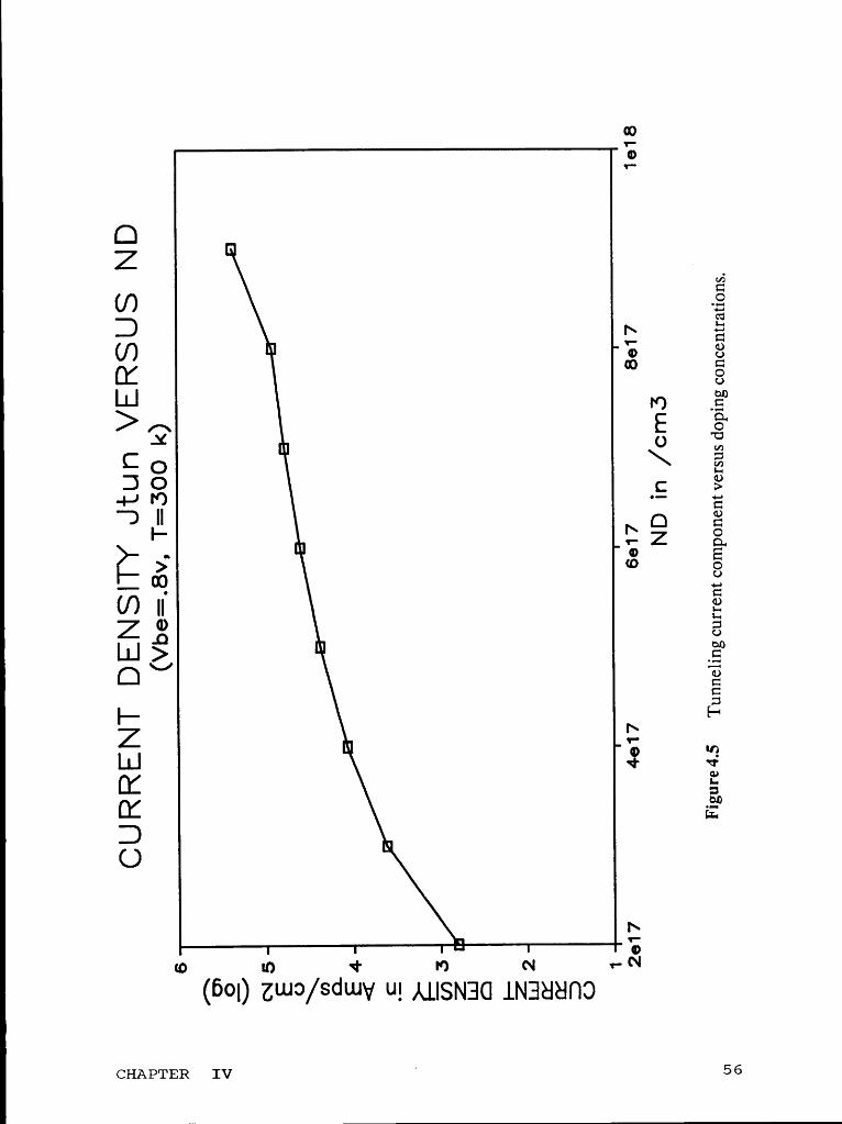
¤lcurrent. However, if the thickness is decreased by increasing the doping concentra-
tion, the tunneling current component increases rapidly. The computation of thetunneling current versus doping concentrations is shown in Figure 4.5. One can
observe that the tunneling current is dominant as the doping concentration exceeds5x1017/cm3. The diffusion-thermionic emission and the tunneling components canbe distinguished by observing their slopes in current-voltage (I-V) characteristics.The latter possesses a greater slope than the former. This is due to the fact that the
tunneling current is a strong function of the applied voltage through both the energy
of the electrons and the thickness of the energy barrier. Therefore, the dominant
injection mechanism varies with the applied voltage range and the doping Concentra-tion of the device.
Figure 4.6 illustrates the current gain ß and Figure 4.7 presents the injection
efficiency 1 and the transport factor wr in the base region. An emitter area of about10‘6 cmz is used to compute the current gain. It can be seen that the current gain ßover the range of the current from 10‘1 to 10‘6 Amperes. is almost constant. This
result is in good agreement with the experimental result reported in reference [24].
The reason for the excellent ß characteristics is mainly attributed to the great
reduction of the recombination current. The low recombination current at theInP-InGaAs interface is due to the excellent lattice match of these two materials.The results also indicate that the magnitude of the current gain ß are strongly
affected by different values of the ratio of the base width to the diffusion length.Actually, this ratio determines the magnitude of the transport factor our, in turn ß,
when the injection efficiency 1 is quite close to one. The ratio is related to the values
within the parenthesis in the expression for Jr. If the diffusion length in such anextremely thin base layer is chosen as 1.3 ,um [31,32], the corresponding ß would be
CHAPTER IV 48
as high as 103. This mainly results from the very short base width and very high
carrier velocity of the injected electrons to transit across the base region in such a
device structure. A thin base layer without buffer between the InGaAs layer and the
InP layer has a very short minority carrier lifetime due to the presence of latticestrain and high density traps. However, the injected electrons go through it only
experiencing a few times of scattering when the thickness of the base region is madecomparable to the carrier mean free path, which is of the order of one hundred A.
The value of the transport velocities at the second "spike" is determined in
terms of the barrier height, the width of the second spike, and the energy that the
electrons possess. The barrier height varies with the doping levels at both the base
and the collector regions, as well as with the applied voltage. The results show that
when the difference in doping level between the two regions is less than 101, the
barrier disappears as the voltage Vbc greater than 2 volts is applied. Therefore, it isnot necessary to consider its effect on the carriers transport. However, if the differ-
ence reaches 102 or larger, the electron blocking action occurring at the secondspike is significant. Figure 4.8 demonstrates that the transport velocities for bothcases are quite low at low voltage range. As the applied voltage increases, the
tunneling transport velocity increases rapidly and eventually reaches the thermal
velocity vth/4, indicating that the tunneling transport is dominant at the high voltagerange. This is mainly due to the decrease of the barrier height and the increase of
the relative energy of the electrons. For low voltage range, the electron blockingaction at the second spike can be eliminated by keeping small difference in doping
levels between the two regions.
CHAPTER IV 49
4.9 Conclusion
The injection mechanisms of electrons from the emitter into the base can be
described by the diffusion, the thermionic emission, and the tunneling theories. It is
important to consider the potential distribution of the energy barrier, especially at
the maximum point, in applying appropriately the diffusion and the thermionic
emission theories. The tunneling current component can be significant for the
injection current at the e-b interface when the doping concentration in the emitter
region is larger than 5x10¹⁷/cm3. The first "spike" at the conduction band disconti-
nuity plays an important role in initiating the injected electrons to enter the base
region with a very high velocity. The electron blocking action of the second "spike"
at the b—c junction at low voltage range can be eliminated by keeping a small
difference in doping level between the base and the emitter regions. Since many
physical factors, which affect the transport process of the injected carriers, are taken
into consideration, the model obtained in this paper is more complete for n-p-nInP/InGaAs abrupt DHBTs. The methods and the results are also useful and
helpful for further theoretical and experimental studies in the future.
CHAPTER IV 50
11
Table 1: Material Parameters Used In The Computations. [33-36]
Parameter Symbol Value
InP bandgap Egl 1.35 eVInGaAs bandgap EC2 0.75 eVConduction band discontinuity A EC 0.20 eVValence band discontinuity A EV 0.38 eVInP effective electron mass m*nl 0.077 moInGaAs effective electron mass m*n2 0.034 moInP permittivity 61 12.8 60InGaAs permittivity 62 11.7 69InP intrinsic carrier concentration nil 107/cmInGaAs intrinsic carrier concentration ni2 1.2x10l2 cm°3InP thermal velocity vthl 4.23x107 cm/sInGaAs thermal velocity Vthz 6.37x107 cm/sInP capture cross section ol 7x10'l6 cm2InGaAs capture cross section o2 3x10'l7 cmzInP capture center density Ntl 3x10l6 cm'3InGaAs capture center density Nt2 1.5x10l3 cm'3Electron diffusion const in base region Un 2.85x10² cmz/s
, Hole diffusion const in emitter region Dp 3.75x10 cmz/sEff. state den. in cond. band of InP NCl 4.16x1017 cm'3Eff. state den. in val. band of InGaAs NV2 1.37x10l9 cm'3State den. of surface recomb of III-V Dst 8x10‘ll cm‘2eV
CHAPTER IV 51
Au—Ge
IIIIIIIIIIIIIIIIIIIA,(///InGaAs 0.2um ¤+ Contact
IIIPj1/. InGaAs P=2xlOl8cm_30.lum Au—Ge ‘
— —
InP N=1xlOl7cm—30.5um
InP N+ BUFFER LAYER
AInP N+ SUBSTRATE
Figure 4.1 Schematic representatiom of the device
structure of 21 n——p—n InP/IhGaAs/InP DHBT
CHAPTER IV 52
II
n—InP __I·_p—IBBGaASL
1 1 —LAB 1qvbl I I I { C I \qvfl I i.
I ICVPII I II I I I
I I II I I II I I IXA XBIX2 X3
Figure 4.2 The energy band diagram forn—p-n InP/InGaAs/InP DHBT
CHAPTER IV 53
¤¤a<1> I-O I> : 0</> I éo3 : .„
: °;2>: § ä
T I.2wwI B
I ~r > E: ° äE:InIZI äLI.! ¤ 30I-I ¤e €
Z - äLz.I I azÜ! ICK :I0 I' O
i' N O N ü' (0 III OI I I I T(ö<>I> zw/Sdwv U! Museen means
CHAPTER IV 54
..0.0.D.O.DLLILI.||.I.IuJ|.IJ·1.*‘!*‘2't“2LllllIIIJLIJLLILLILIJ
:2 °‘!
0 §*’ \-I-J I_‘"J :‘
LI. II · 2 *9 gg
wö:9*6: §2I- · . I 2%
C I E „.,(f)Q I o"'°f+'j I I-. *5 Gmg I O 0 Q•-• ; > OD cw|_L|L.. _¤ ·;·_
L I ~ <I' ·Z·‘ cuI-? ·‘ mE 2 _;
IO I q) ät:JZ 3<(:*:i ' -0 _ä ¤>0;; I > 2- s°
< : ‘ EIä =E · 22 Eä I
II""‘ I
: .IIII
OO O O O O O" T T' '? T(’ö¤I) zw/Sdwv ¤1 MISNHG II~1:—122n0
CHAPTER IV 55
CDE
liZm
[\ g
U) ·‘ E §vu E> 2 .. E 2
c O \ ä3 O c tgä "I " 2
h N 2 äNä ‘° 2
2IDLLIucn‘“I-zi"
Z „ E2
Hä *äazO °
. '.EID IO <I‘ F) N «-gl
(¤¤I) zwv/Sdwv ¤1 Muswao maaano
CHAPTER IV ' 56
-92\$35
*—HT};
Z
-°II¤0
LL}
5—¤¤crääé
0:gg}
:9+DC
_1;0*6OZ
7*
ES
'
ggäLl-]>
N
>I
'
‘:
..
'°
#5
<:0
OSSSE
Lu3L9
(0
gj,
‘“
'
SE
{—·§:
IN N388
F
*So ¤·
Ql
57
o 0 o\ \ \• ~· F) IO
t II I IN .0 .0 .0. 5 5 5Q \ \ \.¤ .¤ .¤Z 3 3 E“+ + + +O1-O III 1 0„-D
I >Z Il ¤ äESI I I Q Ecn 6I- II · f JE0 *66 I > ä«
II ‘•E—!
0 Q1L1. I ¤ 6L1. ¤• · Y > EL1.I $3
I‘6
Z ll·0I.. EP |\1O 2:u.!°*Z
\Q ·°I•· Q (O <I' N IOo ¤> ¤¤ r~ 0 ¤>„: °2 °! °% °! °
CHAPTER IV 58 I

äL1.| ä
1
>£.„ 2
Z·· <ZZ w6·? 22OL1.](D E
L1.|H*—
9F
H<lbQ)
E:M
ä0E—-2 .2
OM
g ä E
Q
2 2 2
U°‘U
LI.]¤
_E ..6 ä
>
‘°B 2
¤
>C> .2
E
2m”
ä féi
Z
"‘ *9
E?
=ij
1-
°‘ ä2:
I\ (D In6 ·¢(°')S/w<>¤1”° ~¤
‘M-|ÖO'|]^F 6
59
I
I
CHAPTER V
Considerations in Microwave Applications
5.0 Introduction
In practical applications, the requirement of bipolar transistor’s high current
gains is not the main interest. Except some special cases, a ß value of around 100 is
good enough. Therefore, the significant benefit from HBTs is its ability to optimize
its performances at higher level. The most important performance that is to be
optimized is the one at high frequency or at microwave frequency.
It is author’s intention to conduct research, as continuation of the present
work, on application of microwave techniques to characterize HBTs in future. To
serve as this purpose, a brief survey of special considerations of HBTs in microwave
applications is given.
5.1 General Requirements of performance at High Frequency
The cutoff frequency fT is an important figure of merit for a microwave
transistor. fT is defined as the frequency at which the common emitter short—circuit
current gain hfb( = 8Ic/8 Ib) is unity. Actually, f-I- describes the ability to possess
current gain at high frequency. It is well known that ß value is
frequency—dependent. ß decreases as frequency increases. This dependence is due
to various effects of capacitance and resistance through the whole transport process.
These effects can be described as RC charging—discharging process. ß value isdetermined by the lost portion of the injected carriers from the emitter. The more
CHAPTER V 60
l
injected carriers lost, the less the ß value. The lost injected carriers due to the
increase in frequency are considered as the contribution to the discharging current
of RC effects. Obviously, higher frequency results in larger discharging current,
leading to the decrease in ß. Therefore, microwave transistor is required to have
current gain at high frequency, implying high fT.
Another important figure of merit is the maximum oscillation frequency fmax,
which is defined as the frequency at which unilateral gain becomes unity. The
unilateral gain is the forward power gain in a feedback amplifier with its reversepower gain set to zero. Therefore, fmax describes the performance of the power
gain of the transistor at high frequency. Sometimes, fmax is called the unity power
gain frequency while fT is called unity current gain frequency. Since the output
impedance of a transistor is higher than the input impedance, the transistor can stillpossess the ability of power amplification even at the condition when the current
gain is unity. For a microwave transistor, it is needed to deliver power output to the
load. Therefore, the transistor is required to have power gain at high frequency,
implying high fmax.
Noise figure is another important figure of merit for microwave transistors.
The noise figure is the ratio of total mean-square noise voltage at the output of the
transistor to mean-square noise voltage at the output resulting from thermal noise
in source resistance. lt is understandable to require the transistor to have small
noise figure. The noise figure is of great concern at high frequency as compared to
lower frequency case since the noise figure increases approximately as f2 .
CHAPTER V 61
5.2 Transit Time T Evaluation
As mentioned above, fT is the one of the important figures of merit of HBTsat high frequency. The cutoff frequency fT is related to the physical structure of thetransistor through the emitter—to—collector delay time, or the transit time T by:
1fT = -1-* (5*].)
2 Tr T
The transit time is actually the sum of four delays encountered sequentially by
the carriers as they flow from the emitter to the collector [23]:
T = Te + Tb + TC + T'C (5-2)
where:T C is the emitter transit time. T C is of the form,
Te = rC(CC + CC)
= kT/qIC(CC + CC) (5-3)
Tb is the base transit time. Tb is of the form,
Tb (5-4)
T C is the collector depletion transit time. T C is of theform,
TC = Xbc/2VSat (5-5)
T ’C is the collector region transit time. T ’C is given by,
CHAPTER V 62
where fc =kT/qlc is the emitter resistance, Cc and Cc are the emitter capacitanceand collector capacitance, respectively, xbc is the depletion width of the b—c junc-
tion, Vsat is the field drift saturation velocity, and fc is the collector series resistance.
The maximum oscillation frequency fmax, as expected, is related to both thecutoff frequency and the RC constant of the combination base resistance—collector
capacitance. fmax is of the form,
lfmax4vr
where UT ¤ 2vrfT and rbb> is the base transverse resistance. Although a questionabout the accuracy of equation (5-7) is raised recently [36,37], the equation does not
lose its significance in analyzing high frequency ferformance of transistors due to its
intuitive expresion.
When HBTs are used as switching transistors, the switching time vS is the
parameter to describe the transit process. The switching time v S is given by:
5 rbb 1vs = i rbbvcc + —— vb + (3CC + CL)RL (5-8)
2 rc
where CL and CL are the load resistance and the load capacitance, respectively,
From the view of the design considerations, most of the requirements of the
CHAPTER V 63

physical structure of the device are the same to all these figures of merit of micro-
wave transistors and high speed transistors. However, individual of these figuresneeds to be considered when the performance of the transistor is optimized.
Considerations in optimization will be discussed later.
5.3 Special Device Design Considerations [12,23,25]
The general design considerations of microwave transistors can be classified
into two aspects: the reduction of the device dimensions and the selection of
materials and configuration. At the present time, advanced technologies have made
it possible to reduce the horizontal dimension to submicron and the vertical dimen-
sion to a few hundred angstrons. For HBTs, special considerations should be taken
in the selection of the material parameters and the device configuration.
1. For a microwave transistor, the main interest is the high frequency output
power, or the increase in fmax. The increase in the base doping actually results in
two benefits. One is the great reduction of the base resistance r’bb, which in turncauses an increase in fmax, according to equation (5-7). The second benefit is that
the reduction of the base resistance leads to a high current density capability, which
improves the tradeoff between speed and power of the wicrowave transistor. The
limitations to the increase in the base doping comes from two aspects: the technolog-
ical constraints and the need to keep the minority lifetime in the base above 10‘10s.
2. Besides the base resistance, the increase in the base doping also results in
the optimization of the emitter capacitance. Since the heterojunction permits theindependence of ß on both the base doping and the emitter doping, a drop in emitter
CHAPTER V 64
1
doping is possible. For a highly unsymmetrically doped p—n junction, it is well
known that the capacitance is considered to be only a function of the lightly doped
level. When the emitter doping drops below the base doping, the emitter capaci-
tance can be represented in the form:
ce ¤¤ ND.}/2 (5-9)
Obviously, a significant reduction can be obtained when the emitter doping is
greatly dropped. From equations (5-1) - (5-3) and equation (5-7), the reduction of
emitter capacitance causes an increase in the cutoff frequency and, in turn, makes
improvement of microwave performance. Also, the reduction of the emitter
capacitance leads to great reduction of the noise. The limitations to the lowest
emitter doping are the effect of the series emitter resistance and the crystal achiev-
able low purity.
3. The base resistance actually consists of two parts: the inner base resistance
and the outer base resistance. The inner base resistance is the portion underneath
the emitter, while the outer base resistance is the portion between the edge of the
emitter and the base contacts. The heavily doped base reduces greatly the inner
resistance, as discussed above. The significance of the outer base resistance depends
on the device configurations. For a heterojunction transistor, the geometry can be
made like the one shown in Figure 5.1. In this configuration, the wide—gap emitter is
constructed as an island, in which the outer base resistance is greatly minimized. A
similar configuration is the mesa configuration, which is shown in Figure 5.2.
However, these configurations result in difficulties encountered in the manufactur-
ing technology, and as a result the realization cost is higher. To avoid the extra
CHAPTER V 65
VV0
effort to minimize the outer base resistance, an alternative configuration is the onewith the wide—gap emitter extended beyond the emitter edge, forming a part of thebase which is a p—n homojunction. This configuration is shown in Figure 5.3. Thisconfiguration, actually being similar to homojunction bipolar transistor, can be easilyrealized. The wide—gap layer with relatively low n—type is first grown as the emitter.The part outside the emitter is then heavily p—type doped to form wide—gap base.The energy diagram for this wide—gap emitter—base homojunction is shown inFigure 5.4, in which it can be seen that the injection current through this wide—gapportion is negligible, compared to the wide—narrow portion, due to the extra barrierof AEg.
4. The concept of the emitter—base junction can be made as wide—gap junction
which does not affect the injection current density gives rise to the inverted collector
configuration, shown in Figure 5.5. In this inverted transistor, the emitter has a
larger area than the collector. In other words, the collector can be made much
smaller area, implying a significantly small collector capacitance. Practically, thereduction of the collector capacitance Cc has more significant effects of improvingthe high frequency performance. These beneficial effects can be recognized byanalyzing equation (5-1) — (5-8).
5.4 Construction of Network Model
More and more computer software packages have been developed to aid the
microwave characterization techniques. For example, Touchstone[39], developed by
EEsof, features a variety of simulation of RF/microwave designs and measurements.It possesses a list of RF devices, transmission lines, and lumped elements models.
u
V CHAPTER V 66

Simulation of S-parameters for two-port or four-port models gives rise to theevaluation of microwave performance of these models in the frequency domain.MTCAP( Modified Transient Circuit Analysis Package), developed by the TimeDomain Laboratory at Virginia Tech [40], is designed for simulation of microwavecircuit’s transient performance in the time domain. With Time Domain Reflecto-metry, an iteration technique can be used to obtain microwave device models. Basedon knowledge of physical nature of the device to be modeled and the results ofmeasurements, the configuration of the device using both lumped and distributedcircuit elements is to be devised. Then, computer-fitting results in an accuratemodel, which can be used to compute the microwave parameters of the device and todesign microwave circuit.
The first step which is involved in characterization of microwave devices is tounderstand the structure of the devices and their physical nature. Usually, terminalparameters of the devices can be measured. However, some physical parameters,which are used to describe internal physics of the devices, are not easily known.Although it is difficult to accurately relate the physical models to the electronicmodels of the devices, it is necessary to possess knowledge of physical models of thedevices and related parameters before attempting to characterize the devices.Models developed under the condition of DC and/or low frequency are consideredto be the basis on which microwave models are to be developed. Effects occurring atmicrowave frequencies are added by introducing lumped and distributed elements.These effects then can be evaluated and modeled by measuring the characteristics ofthe devices, such as S-parameters and impulse response.
The essential operation in HBT is that the current collected by the output
CHAPTER V 67
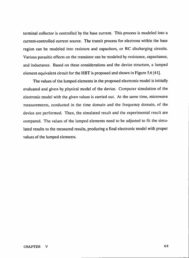
terminal collector is controlled by the base current. This process is modeled into acurrent—controlled current source. The transit process for electrons within the base
region can be modeled into resistors and capacitors, or RC discharging circuits.Various parasitic effects on the transistor can be modeled by resistance, capacitance,
and inductance. Based on these considerations and the device structure, a lumpedelement equivalent circuit for the HBT is proposed and shown in Figure 5.6 [41].
The values of the lumped elements in the proposed electronic model is initiallyevaluated and given by physical model of the device. Computer simulation of theelectronic model with the given values is carried out. At the same time, microwave
measurements, conducted in the time domain and the frequency domain, of the
device are performed. Then, the simulated result and the experimental result arecompared. The values of the lumped elements need to be adjusted to fit the simu-
lated results to the measured results, producing a final electronic model with propervalues of the lumped elements.
CHAPTER V 68
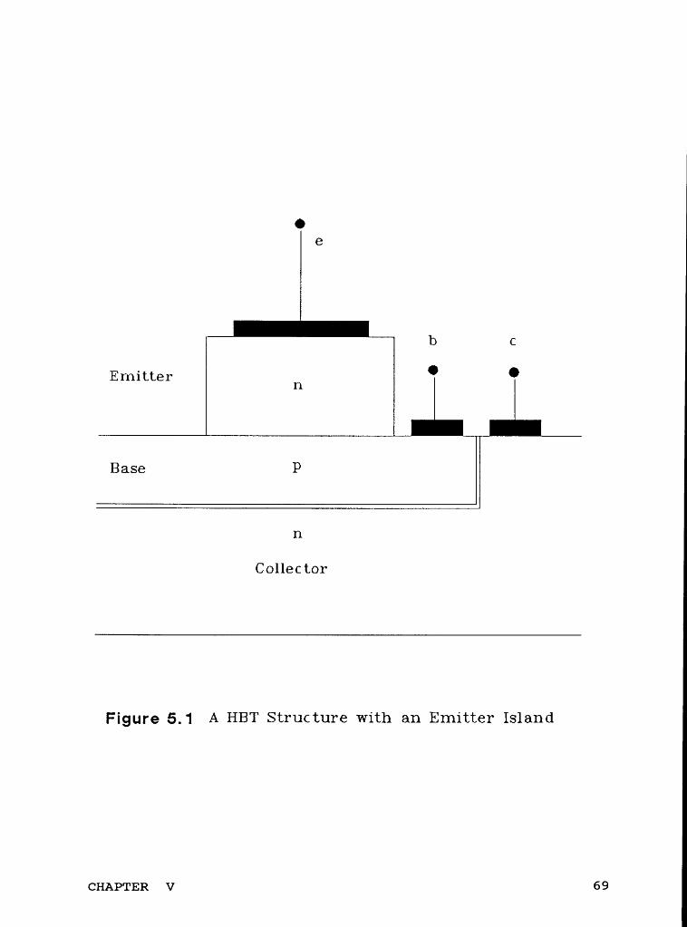
Oe
b c
Emitter• •
n
Base P
n
Collector
Figure 5,1 A HBT Structure with an Emitter Island
CHAPTER v 69
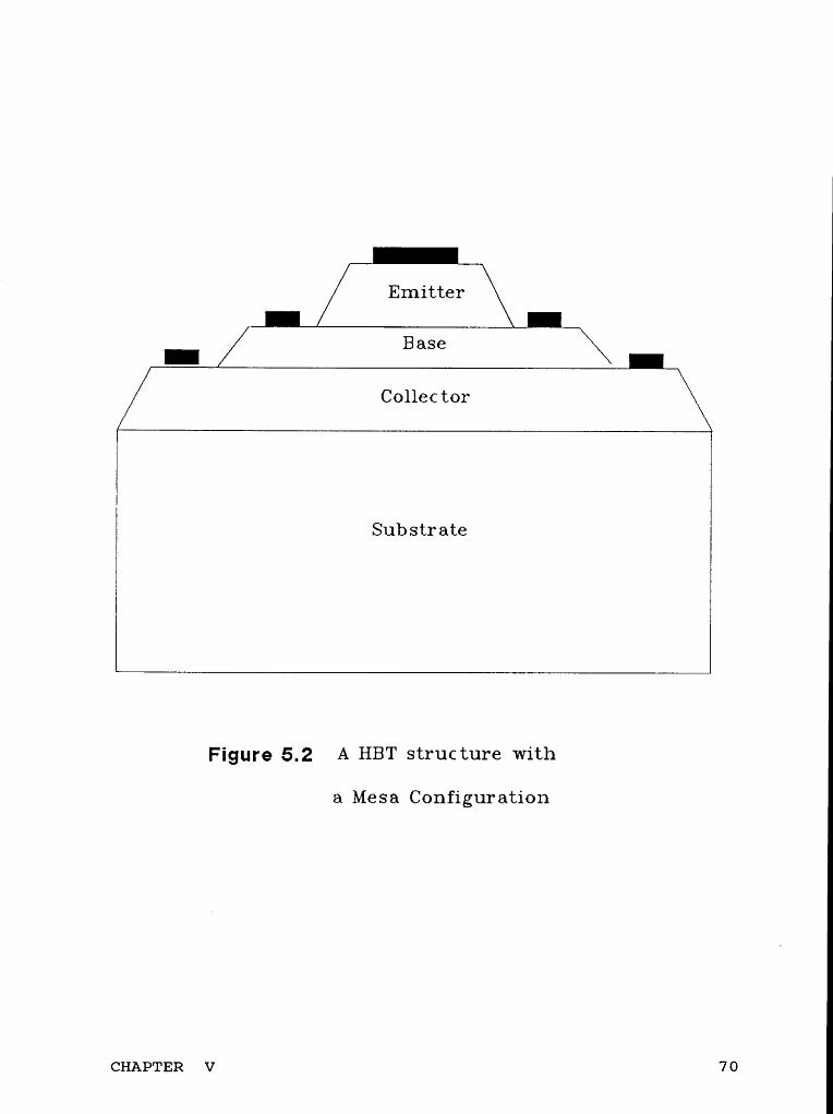
Base1Collector
Substrate
Figure 5,2 A HBT structure With
a Mesa Configuration
cHA1=•TER v 70
Base 6 b CWide Emitter HGap I1
Narro _Gap H
Collector
Figure 5,3 Ari Emitter Structure with aWide Gap Base, Formirig ap-ri Homojuuctiori.
ICHAPTER v 71
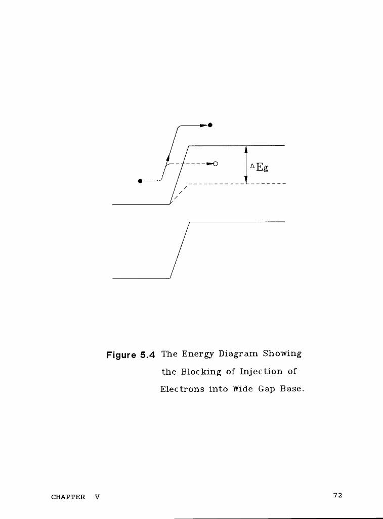
„ •
• ___________ _______/
//
Figure 5_4 The Energy Diagram Showing
the Blocking of Injection of
Electrons into Wide Gap Base.
cHA1;>TER v 72
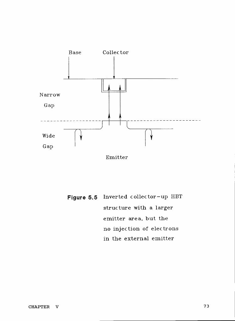
Base Collector
NarrowGap
WideGap
Emitter
Figure 5_5 lnverted collector—up HBT
structure with a larger
emitter area, but theno injection of electronsin the external emitter
CHAPTER V 73
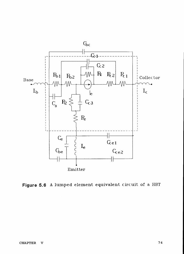
G)C
.— ———————————————Lk-1-——————————-— -7II II @2 gI II R2 1 : Collector
Ib I I6 I I«I CS R2 @6 IQ II II R6 g
C6 I IC QelI6Cbe
I E @62
Emitter
Figure 5_6 A lumped element equivalent circuit of a HBT
CHAPTER V 74
CHAPTER VI
Conclusion and Future Directions
Based on the fundamental knowledge of Heterojunction Bipolar Transis-tors(HBT) provided in the first three chapters, a thorough investigation of mecha-nisms of carrier injection and transport for an HBT is conducted. The followingconclusions are derived:
1. The injection mechanisms of electrons from the emitter into the base can bedescribed by the diffusion, the thermionic emission, and the tunneling theories. It isvery important to consider the potential distribution of the energy barrier, especially
at the point of the maximum, in applying appropriately the diffusion and the ther-
mionic emission theories.2. The tunneling current component can be significant for the injection current
at the e-b heterointerface when the doping concentration in the emitter region is
larger than 5x10¹⁷/cm3. In such a case, the tunneling current component should be
taken into consideration in order to accurately describe the current injection at thee-b junction.
3. The first "spike" at the conduction band at the e-b heterointerface plays animportant role in initiating the injected electrons to enter the base region with a veryhigh velocity. This launching action greatly reduces the electrons transit time as well
as provide a proper boundary condition for the solution of non—equilibrium carrier
distribution, which essentially determines the carrier transport within the base
region.
CHAPTER VI 75

r
4. There is an electron blocking action at the second "spike" at the b-c hetero-junction. This blocking action becomes insignificant as the reverse voltageincreases. At low voltage range, this blocking action can be eliminated by keeping asmall difference in doping level between the base and the emitter regions.
5.The physical model obtained is more complete for n-p—n InP/InGaAs/InPabrupt DHBTs since many physical factors that affect the carrier transport are takeninto consideration. Therefore, the model provide the future research on HBTs witha fundamental basis.
As suggested in Chapter V, the following topics are considered to be suitablefor future research:
1. Extend the obtained one—dimensional model to two-dimensional case ,
where more practical simulations are needed.2. Relate the physical model to an electrical network model, which consists of
electrical lumped elements.3. After the network model with lumped elements is set up, microwave
characterization techniques are applied to evaluate the high frequency performanceof these devices.
4. Develop techniques, both theoretical and experimental, for characterizationof HBTs in microwave frequency.
CHAPTER VI 76

l BIBLIOGRAPHY
1. R.M. Kolbas, N.G. Anderson, W.D. Laidig, Yongkun Sin, Y.C. Lo, K.Y. Hsieh,
and Y.J. Yang, " Strained—Layer InGaAs-GaAs-AlGaAs Photopumped and
Current Injection Lasers." IEEE J. Quantum Electronics,Vol. 24, No. 8, p 1605,
August 1988.
2. A. Furuya, M. Makiuchi, O. Wada, and T. Fujii, " AlGaAs/GaAs Lateral Current
Injection Multiquantum Well (LCI-MQW) Laser Using Impurity-InducedDisordering," IEEE J. Quantum Electronics, Vol. 24, No. 12, p2448, December
1988.
3. D. Wake, L.C. Blank, R.H. Walling, and I.D. Henning, " Top—Illuminated
InGaAs/InP p-i—n Photodiodes with a 3-dB Bandwidth in Excess of 26 GHz,"
IEEE Electron Device Letters, Vol.EDL-9, No.5, pp.226 - 228, May 1988.
4 H. Hulu and H. Morkoc, " Modulation-doped FETs and Other High Speed III-VTransistor," SPIE, Vol. 795, pp.12 - 28, 1987.
5. W. Schockley, U.S. Patent 2,569,347 (1951).
6. H. Kroemer, " Theory of a Wide-gap Emitter for Transistors," Proc. IRE, Vol. 45,
p 1535, 1957.
7. S.R. McAfee, D.V. Lang, and W.T. Tsang, " Observation of Deep Levels Asscoci-
BIBLIOGRAPHY 77
ated with the GaAs/AlXGa1_XAs Interface Grown by Molecular Beam Epitaxy,"
Appl. Phys. Letters, Vol. 40, No. 6, p 520, 1982.
8. R.N. Nottenburg, H. Temkin, M.B. Panish, and R.A. Hamm, " High Gain
InGaAs/InP Heterostructure Bipolar Transistor Grown by Gas Source Molecular
Beam Epitaxy," Appl. Phys. Letters, Vol. 49, No. 17, pp. 1112 - 1114, October 27,
1986.
9. R.N. Nottenburg, Y.K. Chen, M.B. Panish, D.A. Humphrey, and R. Hamm, "
Hot—Electron InGaAS/InP Heterostructure Bipolar Transistors with fT of 110
GHz," IEEE Electron Device Letters, Vol. EDL—10, No. 1, pp. 30 - 32, January
1989.
10. K. Tomizawa, Y. Awano, and N. Hashizume, "Monte Carlo Simulation of
AlGaAs/GaAs Heterojunction Bipolar Transistors," IEEE Electron Device
Letters, Vol. EDL-5, No. 9, p 362, September 1984.
11. K. Tomizawa, Y. Awano, N. Hashizame, and M. Kawashima, " Simulation of
Near Ballistic Electron Transport in a Submicron GaAs Diode with
AlXGa1_XAs/GaAs Heterojunction Cathod," IEE Proc. 132, Pt. 1, No. 1, p 37,
1985.
12. H. Kroemer, " Heterostructure Bipolar Transistors and Integrated Circuits,"
Proc. IEEE, Vol. 70, No. 1, January 1982.
13. H. Kroemer, " Heterostructure, Bipolar Transistors: What Should We Build? ," J. K
BIBLIOGRAPHY 78
Vaccum Science Technology, Vol B1, No. 1, pp 126 - 130, June 1983.
14. J.L. Peloward, R. Castegne, and P. Hesto, " Monte Carlo Study of Ballistic
Transport in Heterojunction Bipolar Transistors (DHBJTs) and in High Electron
MObility Transistors (HEMTs) ," SPIE, Vol. 795, 1987.
15. J.P. Bailbe, A.Marty, and G. Rey, " III-V Heterojunction Bipolar Transistors,"
Solid State Electronics, Vol. 30, No. 11, pp. 1159 - 1169, 1987.
16. A.G. Milnes, " Heterojunctions: Some Knowns and Unknowns," Solid State
Electronics, Vol. 30, No. 11, pp. 1099 - 1105, 1987.
17. A.A. Grinberg, M.S. Shur, R.J. Fischer, and H. Morkoc, "An Investigation of the
Effect of Graded Layers and Tunneling on the Performance of AlGaAs/GaAs
Heterojunction Bipolar Transistors," IEEE Transactions On Electron Devices,
Vol. ED-31, No. 12, pp. 1758-1765, December 1984.
18. S.C. Lee, J.N. Kau, and H.H. Lin, "Current Transport Across the Emitter-Base
Potential Spike in AlGaAs/GaAs Heterojunction Bipolar Transistors," J. Appl.
Phys., Vol. 58, No. 2, pp. 890-895, July 1985.
19. A.G. Milnes, "Semiconductor Heterojunction Topics: Introduction And Over-
view," Solid-State Electronics, Vol. 29, No. 2, pp. 99-121, 1986.
20. S.M. Sze, "Physics of Semiconductor Devices," John Wiley & Son, Chapter 5,
pp245-263, 1981.
BIBLIOGRAPHY 79

21. A.G. Milnes and D.L. Feucht, " Heterojunctions and Metal-Semiconductor
Junctions," Academic Press, New York and London, 1972.
22. Y.G. Chai, C. Yuen, and G.A. Zdasiuk, "Investigation of In0_53GaO_47As forHigh-Frequency Microwave Power FET’s," IEEE Transaction on Electron
Devices, Vol. ED-32, No. 5, pp. 972-977, May 1985.
23. S.R. Forrest, P.H. Schmidt, R.B. Wilson, and M.L. Kaplan, "Measurement of the
Conductor Band Discontinuities of InGaAsP/InP Heterojunctions Using Capaci-
tance-Voltage Analysis," J. Vaccum Sciences Technology, Vol. B4, pp. 37-44,
1986.
24. P. Schuitemaker, P.A. Houston, and P.N. Robson, "Progress on InP/InGaAs(P)
Heterojunction Bipolar Transistors," SPIE, Vol. 795, pp. 29-40, 1987.
25. R.N. Nottenburg, H. Temkin, M.B. Panish, R. Bhat, and J.C. Bischoff,
"InGaAs/InP Double-Heterostructure Bipolar Transistors With Near-Ideal ßVersus IC Characteristics," IEEE Electron Device Letter, Vol. EDL-7, No. 11, pp.
613-615, November 1986.
26. C.R. Crowell and M. Hafizi, "Current Transport over Parabolic Potentia Barriers
in Semiconductor Devices," IEEE Transaction on Electron Devices, Vol.ED—35,
No. 7, pp. 1087-1095, July 1988.
27. R. Stratton, "Volt-Current Charactersitcs For Tunneling Through Insulating
BIBLIOGRAPHY 80
Films," J. Phys. Chem. Solids, Vol. 23, pp1177-1190, March 1962.
28. F.A. Padovani and R. Stratton, "Field and Thermionic-Field Emission In
Schottky Barriers," Solid State Electronics, Vol. 9, pp. 695-706, 1966.
29. S.C. Lee and H.H. Lin, "Transport Theory of the Double Heterojunction Bipolar
Transistor Based On Current Balancing Concept," J. Appl. Phys., Vol. 59, No. 5,
pp. 1688-1695, March 1986.
30. H.E. Talley and D.G. Daugherty, "Physical Principles of Semiconductor Devices,"
The Iowa State University Press, Chapter 7. pp199—202, 1976.
31. Y.G. Chai, C. Yuen, and G.A. Zdasiuk, " Investigation of In0_53Ga0_47As forHigh-Frequency Microwave Power FET’s," IEEE Transaction on Electron
Devices, Vol. ED-32, No. 5, pp. 972 - 977, May 1985.
32. M.M. Tashima, L.W. Cook, and G.E. Stiilman, " Minority Carrier Diffusion
Lengths In Liquuid Phase Epitaxial InGaAsP and InGaAs," J. Electronic
Materials, Vol. 11, No. 4, pp. 831 - 847, 1982.
33. S.R. Forrest and O.K. Kim, "Deep Levels In In0_53Ga0_47As/InP Heterostruc-tures," J. Appl. Phys., Vol. 53, No. 8, pp. 5738-5745, August 1982.
34. S.R. Forrest and O.K. Kim, "Analysis of the Dark Current and Photoresponse of
In0_51Ga0_47As/InP Avalanche Photodiodes," Solid State Electronics, Vol. 26,No. 10, pp. 951-968, 1983.
BIBLIOGRAPHY81 g
35. M.J. Ludowise, N. Holongak, P.D. Wright, B.A. Vojak, E.A. Rezek, and H.W.
Korb, "Defect- and Phonon-Assited Tunneling in LPE In1_XGaXP1_ZAsZ DH
Laser Diodes (31 ~ 1 ,um)," J. Appl. Phys., Vol. 48, No. 10, pp. 4287-4291, October
1977.
36. S. Gourrier, P. Friedel, and J.P. Chane, "Interface Properties of
Metal/Oxide/Semiconductor and Metal/Insulator/Semiconductor Structures On
Ga1_XInXAs With x = 0.35 and 0.10," Thin Solid Film, Vol. 103, pp. 155-166,
1983.
37. B. Pejcinovic, T.W. Tang, and D.H. Navon, "High-Frequency Characterization of
Heterojunction Bipolar Transistors Using Numerical Simulation," IEEE Transac-
tions on Electron Devices, Vol.ED-36, No. 2, February 1989.
38. M.B. Das, "High-Frequency Performance Limitations of Millimeter-Wave
Heterojunction Bipolar Transistors," IEEE Transactions on electron devices,
Vol.ED-35, No. 5, May 1988.
40. B. Bayraktaroglu and N. Camilleri, "Microwave Performances of npn and pnp
ALGaAs/GaAs Heterojunction Bipolar Transistors," IEEE MTT-S Digest, pp.
529-532, 1988.
BIBLIGGRAPHY 82 „1