investigation of theoretical limitations of...
TRANSCRIPT

INVESTIGATION OF THEORETICAL LIMITATIONS OF RECOMBINATION
DCIV METHODOLOGY FOR CHARACTERIZATION OF MOS TRANSISTORS
By
ZUHUI CHEN
A DISSERTATION PRESENTED TO THE GRADUATE SCHOOL OF THE UNIVERSITY OF FLORIDA IN PARTIAL FULFILLMENT
OF THE REQUIREMENTS FOR THE DEGREE OF DOCTOR OF PHILOSOPHY
UNIVERSITY OF FLORIDA
2005

Copyright 2005
by
Zuhui Chen
iii
ACKNOWLEDGMENTS
I am deeply indebted to Professor Chih-Tang Sah for his invaluable guidance,
patience and teaching throughout my graduate study at the University of Florida. I would
also like to thank Professors Kevin Jones, Sheng S. Li, Toshikazu Nishida, Scott
Thompson and Bin Jie for serving on my Ph.D. supervisory committee. Special thanks
go to Professors Xiuhua Lin and Binxi Jiang who led me into the field of solid-state
physics when I was a graduate student at Xiamen University in China.
I am grateful to the Chinese Church at Gainesville for giving my family much help
before and after our baby Aden Chen was born on Jan., 27. 2005.
Finally, I would like to thank my wife, Li Wu, for her love, support and
encouragement, and our parents, Shuisheng Chen, Mudi Zeng, Huaxing Wu and Lijuan
Huang, for their continuous support throughout my graduate education.
iv
TABLE OF CONTENTS page
ACKNOWLEDGMENTS ................................................................................................. iii
LIST OF FIGURES ........................................................................................................... vi
ABSTRACT....................................................................................................................... ix
CHAPTER
1 INTRODUCTION ........................................................................................................1
2 THEORETICAL CONFIDENT LEVEL OF BI APPROXIMATION COMPARED WITH THE EXACT FD SOLUTIONS ................................................5
2.1 Introduction.............................................................................................................5 2.2 Configurations of the R-DCIV method ..................................................................8 2.3 Theory of R-DCIV Methodology .........................................................................13 2.4 Theoretical Computations for Confident Level ....................................................23
2.4.1 BI, BD and FI Approximations Compared with FD Exact Theory............29 2.4.2 Dopant Impurity Concentration Dependence.............................................34 2.4.3 Oxide Thickness Dependence ....................................................................41 2.4.4 Injected Minority Carrier Concentration Dependence ...............................47 2.4.5 Energy Position of Discrete Energy Level Interface Traps........................53 2.4.6 Temperature Dependence...........................................................................59
2.5 Summary...............................................................................................................65
3 R-DCIV LINESHAPES FROM DISTRIBUTED ENERGY LEVELS OF INTERFACE TRAPS IN SILICON GAP..................................................................66
3.1 Introduction...........................................................................................................66 3.2 Effect of ratio of electron and hole capture rates at mid-gap trap ........................71 3.3 Effect of Distribution of Interface Trap Energy Level on R-DCIV Lineshape....75 3.4 Temperature Dependence .....................................................................................97
3.4.1. Temperature Dependence of the Peak Current IB-peak................................98 3.4.2. Temperature Dependence of the IB-VGB lineshape..................................107 2.4.3. Temperature Dependence of peak gate voltage VGB-peak .........................113 3.4.4. Reciprocal slope ......................................................................................118
3.5 Summary.............................................................................................................120
v
4 IMPURITY DEIONIZATION .................................................................................122
4.1 Introduction.........................................................................................................122 4.2 Dopant Impurity Concentration Dependence .....................................................126 4.2 Oxide Thickness Dependence.............................................................................130 4.4 Summary.............................................................................................................134
5 SUMMARY AND CONCLUSIONS.......................................................................135
APPENDIX ACCURACY OF ITERATIVE ANALYTICAL SOLUTIONS..............140
REFERENCES ................................................................................................................150
BIOGRAPHICAL SKETCH ...........................................................................................156
vi
LIST OF FIGURES
Figure page 2.1 Schematic device cross section of modern n-channel MOS transistor. .....................9
2.2 Four DCIV bias configurations for a pMOS transistor: ...........................................12
2.3 Energy band diagram and cross sectional view of a gated n+Si/SiO2/p-Si structure in the basewell channel region along x direction. .....................................17
2.4 A transition energy band diagram showing the four fundamental transistion processes between a conduction or valence band state and an electron trap state in the silicon energy gap...........................................................................................18
2.5 (a) Comparison of the theoretical R-DCIV curves between BI, BD, FI, and FD solutions. (b) Normalized percentage deviation with respect to the exact or real FD theory Temperature T=296.15K. Metal gate MOS transistor. ...........................33
2.6 Effect of dopant impurity concentration on the DCIV on the normalized IB vs. VGB lineshape. Metal gate nMOS transistors. ..........................................................37
2.7 Effect of dopant impurity concentration on the DCIV on the normalized IB vs. VGB lineshape. Silicon gate nMOS transistors. ........................................................39
2.8 Effect of oxide thickness on the DCIV on the normalized IB vs. VGB lineshape. Metal gate nMOS transistors....................................................................................43
2.9 Effect of oxide thickness on the DCIV on the normalized IB vs. VGB lineshape. Silicon gate nMOS transistors..................................................................................45
2.10 Effect of injection carrier concentration on the DCIV on the normalized IB vs. VGB lineshape. Metal gate nMOS transistors. ........................................................50
2.11 Effect of injection carrier concentration on the DCIV on the normalized IB vs. VGB lineshape. Silicon gate nMOS transistors. ......................................................52
2.12 Effect of energy position of discrete interface trap energy level on the DCIV on the normalized IB vs. VGB lineshape. Metal gate nMOS transistors......................55
2.13 Effect of energy position of discrete interface trap energy level on the DCIV on the normalized IB vs. VGB lineshape. Silicon gate nMOS transistors....................57
vii
2.14 Effect of temperature on the DCIV on the normalized IB vs. VGB lineshape. Metal gate nMOS transistors....................................................................................60
2.15 Effect of temperature on the DCIV on the normalized IB vs. VGB lineshape. Silicon gate nMOS transistors..................................................................................62
3.1 Energy distribution of Interface traps.......................................................................70
3.2 Effect of ratio of electron and hole-capture rates on normalized IB-VGB lineshape: Interface trap level is at mid-gap.............................................................73
3.3 Effect of ratio of electron and hole-capture rates on normalized IB-VGB lineshape. Density of interface traps is U-shaped and the ratio of cps/cns = CPN. .79
3.4 Effect of discrete and asymmetrical interface trap energy distribution on IB-VGB lineshape .........................................................................................................82
3.5 Effect of two discrete symmetrical interface traps at ETI =±0.05eV on IB-VGB lineshape:..................................................................................................................86
3.6 Effect of two discrete and one mid-gap interface traps on IB-VGB lineshape........91
3.7 Comparison for three distribution of density of interface traps in Si-gap: a U-shaped DOS, a constant DOS and a discrete interface trap energy level at mid-gap ETI=0.................................................................................................................93
3.8 Forward bias VPN dependence of recombination peak current IB-peak for an interface trap with discrete interface energy level..................................................100
3.9 Forward bias VPN dependence of recombination peak current IB-peak for continuous distribution of interface energy level in silicon gap. ...........................101
3.10 Temperature T dependence of recombination peak current IB-peak for ...............102
3.11 Forward bias VPN dependence of thermal activation energy EA for an interface trap with discrete interface energy level.................................................................103
3.12 Temperature T dependence of recombination peak current IB-peak for a discrete interface energy ETI=0, ±0.5eV, with NIT=ƒ(ETI) or NIT≠ƒ(ETI)......................104
3.13 Temperature T dependence of the IB-VGB linewidth for interface trap energy level at mid-gap ETI=0.0eVK................................................................................109
3.14 Temperature T dependence of the IB-VGB linewidth for a U-shaped distribution of interface trap energy level in silicon gap. ..........................................................111
3.15 effect on peak gate voltage VGB-peak from oxide thickness, impurity concentration, trap level, and termperature. ...........................................................115
viii
3.16 Reciprocal slope depends on (a) ETI, and (b) Temperature.. ................................119
4.1 Impurity deionization effect at the SiO2/Si interface in non-compsated range......124
4.2 Impurity deionization effect at the SiO2/Si interface in compsated range. ............124
4.3 Deionization effect of dopant impurity concentration on the DCIV on the normalized IB vs. VGB lineshape..........................................................................128
4.4 Deionization effect of oxide thickness on the DCIV on the normalized IB vs. VGB lineshape.. .....................................................................................................132
ix
Abstract of Dissertation Presented to the Graduate School of the University of Florida in Partial Fulfillment of the Requirements for the Degree of Doctor of Philosophy
INVESTIGATION OF THEORETICAL LIMITATIONS OF RECOMBINATION DCIV METHODOLOGY FOR CHARACTERIZATION OF MOS TRANSISTORS
By
Zuhui Chen
August 2005
Chair: Chih-Tang Sah Major Department: Electrical and Computer Engineering
This dissertation investigates the accuracy of using the recombination direct-
current current voltage (R-DCIV) method to measure the interface traps and spatial
variations or profiles of impurities and oxides in silicon MOS transistors. The Boltzmann
electron-hole distribution and ionized impurity approximations (Boltzmann ionization or
BI) are much faster than the Fermi-Deionizated (FD) model. The accuracy of using the
BI approximation to extract the device and material parameters of an MOS transistor is
investigated by comparing with the time-consuming and complicated FD model. The
accuracies or confident levels on the extractable device and material parameters are
analyzed, such as dopant impurity concentration PAA, oxide thickness XOX, interface trap
concentration NIT, injected minority carrier concentration at SiO2/Si interface represented
by the p/n junction VPN, energy level of interface traps distribution in silicon gap ETI and
temperature T. From R-DCIV lineshape analyses, it is shown that the BI approximation
gives a small (1%~5%) deviation when matching 90% of the experimental DCIV curve
x
to theory. These results indicate that the simple and time-saving BI approximations are
sufficiently accurate to extract from experimental data the spatial profiles of the dopant
impurity concentration, and interface trap concentration at the SiO2/Si interface, and
oxide thickness in modern MOS transistors.
Effects of energy distribution of the interface traps on the R-DCIV lineshape are
also investigated. Comparison are made among three density of state (DOS) distributions
of interface traps (1) a U-shaped DOS, (2) a constant DOS, and (3) a discrete interface
trap energy level at mid-gap. These comparison shows that the experimental broadened
R-DCIV lineshapes may also be accounted partially for the spatial variation of surface
dopant impurity concentration but also by the energy distribution of interface traps in
silicon gap. Slater’s perturbation theory is employed to suggest that a U-shaped DOS is
the most probable distribution in silicon gap. Thus, the extractions of parameter spatial
profiles, from experimental, should use a U-shaped density of interface traps, instead of
the commonly assumed trap level at mid-gap ETI=0 in the silicon energy gap.
For both the continuous energy distribution of interface traps and a discrete
interface trap energy level at midgap, the peak R-DCIV current has large temperature
dependence. However, the thermal activation energy, the lineshape, reciprocal slope, and
peak gate voltage all have negligible temperature dependence. The analyses of impurity
deionization effect show that deionization has a negligible effect on the R-DCIV
lineshape when using Fermi ionization approximation (FI) to match experimental data
from peak current down to 10% of the peak. The errors of FI approximation are nearly
identical to the confident level of BI for all device and material parameters in practical
range, for both metal gate and silicon gate MOS transistors.
1
CHAPTER 1 INTRODUCTION
Today, the metal-oxide-semiconductor (MOS) transistor has become the most
important building block of ultra-large-scale-integrated (ULSI) circuits. The dimension of
MOS transistors has narrowed from 25um in 1962 [1] to 90nm in 2002 [2]. The scaling
trend, propelled by the rapid advancement of VLSI technology, is expected to continue
[3] and the MOS transistor in production may shrink to 50nm in 2012 [4] as projected by
the 1999 International Technology Roadmap for Semiconductors (ITRS).
The success of today’s semiconductor industry can be partially if not dominantly
attributed to the extremely low density of electron-hole recombination, generation and
trapping centers or traps at the SiO2/Si interface (interface traps). Routine manufacturing
processes have reduced the interface trap concentration NIT to 1010cm-2 by slow cooling
after the final high temperature oxidation step and by post-oxidation annealing in
hydrogen. The traditional small-signal measurement techniques such as the MOS
capacitance voltage method can only resolve interface trap density higher than about
1011cm-2 and not its spatial variation and can not detect the very low density
manufacturing residual interface traps in the state-of-the art MOS transistors.
Recombination Direct Current Current-Voltage (R-DCIV) methodology is a simple and
sensitive tool to extract spatial variation or profile of dopant impurity concentration and
interface trap concentration profiles and oxide thickness. The high sensitivity is attained
by forward-biasing one or more p/n junctions (VPN) in a MOS transistor to exponentially
raise the injected minority carrier concentration, exp(qVPN/kT). In this dissertation, the
2
differences among BI, BD, FI, and FD solutions will be analyzed to determine the
accuracy of the BI approximation which is computational the fastest. Here, BI stands for
Boltzmann distribution of electrons and holes in energy and impurity full ionization. BD
stands for Boltzmann distribution and impurity Deionization. FI stands for Fermi
distribution of electrons and holes and impurity full ionization. FD stands for Fermi
distribution and impurity deionization. We will evaluate the accuracy of simple and
computational time-saving BI approximation solutions by comparison with the exact,
complicated and time-consuming FD theory. One of the novelties is that R-DCIV
lineshape is very sensitive to the device and material properties but rather insensitive to
multi-dimensional effects inherent in the very small transistors.
In chapter 2, the current in the base terminal of the MOS transistor IB, as a function
of gate voltage VGB, due to electron-hole recombination at the SiO2/Si interface traps in
the basewell channel region, is analyzed theoretically using the Shockley-Read-Hall
steady state recombination kinetics which has been applied by us [5-21]. Families of
theoretical IB -VGB curves are presented to illustrate their dependencies on the variations
of dopant impurity concentration, oxide thickness, injected minority carrier
concentration, interface trap energy level and temperature. The percentage deviation as a
function of gate voltage and %RMS deviation over a range gate voltage covering the
peak current are used to evaluate the accuracy of simple and time-saving BI
approximation, by comparing with the exact, complicated and time-consuming FD
theory. According to these accuracy or confidence levels, it is shown that extracted value
from experimental data would have only a small error from using BI approximation when
matching 90% of the experimental R-DCIV curve from peak current IB-peak down to

3
10% of the peak. The comparison of BI, BD, FI and FD solutions indicates that BI and FI
solutions are respectively nearly as good as the BD and FD solutions, and the
deionization only has effect on DCIV lineshape in accumulation region for n-MOS
transistors. This R-DCIV lineshape analysis gives a comprehensive baseline that can be
used to guide the analysis when extracting the spatial profiles of the impurity
concentration, interface trap concentration and oxide thickness from the experimental
data. This simple and nondestructive R-DCIV methodology provides a powerful
capability for routine monitoring and feedback during transistor fabrication.
In chapter 3, the effect on R-DCIV lineshape of electron and hole capture rates at
mid-gap is analyzed. It shows that the ratio assumption with 0.01<cns/cps<100 at mid-
gap has a small effect on the lineshape. Family of curves are computed to illustrate the
effects on R-DCIV lineshapes from the three distributed energy level of interface traps in
silicon gap: (1) a U-shaped DOS, (2) a constant DOS, and (3) a discrete interface trap
energy level at mid-gap. Comparisons among these distributions indicate that the
broadened lineshape in experiments can also be accounted for partially by the energy
distribution of interface traps in silicon gap, not just the spatial variation of surface
dopant impurity concentration. Based on Slater’s perturbation theory, we conclude that
the most probable density distribution of the interface traps in the silicon energy gap is U-
Shaped. This is from the random variations of bond length and bond angle of the Si::O4.
Thus, the theory to extract impurity concentration and interface concentration profiles
should be modified from the traditional assumption of interface energy level at mid-gap
ETI=0, to a U-Shaped density distribution of interface traps throughout the energy silicon
gap.
4
The forward bias VPN dependence of peak gate voltage VGB-peak, thermal
activation energy EA and peak current peak current IB-peak can provide a determination
of the effective interface trap energy level ETI* for discrete interface trap levels. For both
discrete and continuous interface trap level, EA, IB-peak, VGB-peak, n, and IB-VGB
lineshape have negligible temperature dependence, while IB-peak has large temperature
dependence.
In chapter 4, impurity deionization dependence of dopant concentration and oxide
thickness on R-DCIV lineshape will be analyzed. The percentage deviation and %RMS
deviation of Fermi ionization approximation (FI) show that there is a negligible impurity
deionization near the SiO2/Si interface in MOS transistors when matching 90% of
experimental data from peak current down to 10% of the peak. We can expect that the
errors of FI approximation are nearly identical to the confident level of BI for other
device and material parameters in practical range, such as injected minority
concentration, interface trap energy level and temperature, for both metal gate and silicon
gate MOS transistors. The analyses of impurity deionization confirms that the time-
saving and simple BI is a good approximation to extract the spatial profiles from
experiment data, such as the dopant impurity concentration, interface trap concentration,
oxide thickness since it has a good physical basis at around the recombination peak
current.
Chapter 5 gives the summaries and concludes this dissertation.
5
CHAPTER 2 THEORETICAL CONFIDENT LEVEL OF BI APPROXIMATION COMPARED
WITH THE EXACT FD SOLUTIONS
2.1 Introduction
Recombination-DCIV (R-DCIV) methodology is a reliable and powerful tool for
diagnosing interface properties as well as for characterizing transistor design. It is the
only method which can extract profiles of the channel impurity concentration and oxide
thickness with high resolutions in nanometer dimension range. However, its accuracy has
not been evaluated. As we already know, the BI approximation solution is time saving
and simple compared with the time consuming and complicated FD solution. There are
some possible sources of errors using BI approximation in extracting parameters from
experimental R-DCIV data such as impurity and interface trap concentration profiles and
oxide thickness profiles. In this chapter, we will evaluate these errors and present the
confident level of BI approximation by comparing the BI and BD results with those of
FD.
The principle of R-DCIV is the use of a surface-potential-controlling gate terminal
voltage, VGB, to modulate the base-terminal DC current, IB, from electron-hole
recombination at the SiO2/Si interface traps. The lineshape, linewidth, peak gate voltage
and peak amplitude of the recombination currents from electron-hole recombination at
the interface traps in the channel space charge region are analyzed using Shockley-Read-
Hall steady-state recombination kinetics. The material physics used in this thesis are
6
based on the textbook of Sah [5,6] and references cited therein, including previous work
on R-DCIV [7-21] .
Compared with the widely used differential C-V profiling method, the R-DCIV
profiling technique provides several advantages: (1) low sensitivity to gate area variation;
(2) no special test structures required to perform the test – all production MOS transistors
can be used with sufficient sensitivity and resolution; (3) direct-current (DC)
measurements allowing long-time average to reduce noise and increasing sensitivity
using simple computer-controlled digital data collection; and (4) the test is
nondestructive. Its high sensitivity is derived from forward-biasing one of the p/n
junctions to greatly increase the minority carrier concentration and recombination rate. In
MOS transistor structures, it gains further sensitivity from the common-emitter and
common-base current gain of the BJT which is present in all MOS transistor structures.
Sah [7, 8] measured the R-DCIV characteristics of MOS-gated silicon bipolar
transistors in 1961 to investigate the effects of surface recombination and channel on p/n
junction and transistor characteristics. The R-DCIV method was reactivated 35 years later
by Neugroschel et al. [9] in 1995 as a sensitive monitor for transistor reliability. They
investigated the generation kinetics of the interface traps and the degradation kinetics of
electrically stressed transistors from electrical-stress-created oxide and interface traps.
In the past several years, many R-DCIV applications were reported which included
the delineation of interface trap generation/annealing kinetics on electrically-stressed
transistors by hot carriers and high current densities, and diagnosis and evaluation of
transistor design and manufacturing processes on pre-stress transistors [10-25].
7
In this chapter, the characteristics of the surface electron-hole recombination
current in the channel region are studied theoretically and the confident levels of
Boltzmann Ionized approximation solutions are computed in order to provide a
comprehensive baseline that can be used to guide the analyses of experimental data in the
applications. These results can help quantify the applications of the simple and time-
saving BI solutions for the extraction of fundamental and application-specific properties
of transistors and their materials, such as the physical (spatial location and density) and
electronic (quantum density of states) properties of the residual and stress-generated
interface and oxide traps, and the dopant impurity concentration profiles. The formulation
includes high injection level in the quasi-neutral basewell and electrical non-equilibrium
from the forward applied p/n junction voltage which gives NP > ni2. Analytical solutions
and their physical models are presented to illustrate the effects of material parameters on
the IB-VGB lineshape, the amplitude of peak current IB-peak, and peak gate voltage VGB-peak
at the IB-peak.
Families of base current versus gate/base voltage (IB-VGB) are computed to
illustrate the effects of the bulk impurity concentration and interface trap properties on
the lineshape and the (IBpk, VGBpk) location and IB magnitude. The systematic
computation begins with the ideal transistor structure in which there is no spatial
variation of the basewell impurity concentration and a discrete energy distribution of
interface traps is at mid-gap ETI=0. The simple ideal model can allow us to extrapolate
the BI confident levels when extending to include spatial variations of dopant impurity
interface trap concentrations, injected minority carrier concentration, and a U-shaped
density distribution of interface traps in silicon gap.
8
2.2 Configurations of the R-DCIV method
One of the most important DCIV applications is to extract the surface dopant
impurity profile at the interface of SiO2/Si. As the transistor dimensions decrease, the
conventional optical and traditional electrical methods are increasingly inaccurate to
monitor and measure the impurity profiles. The major difficulty lies in having as accurate
a measurement to monitor impurity profiles in order to provide the feedback necessary
for iterative fabrication processing to attain the optimum impurity profile and transistor
characteristics to maintain or improve the high-performance electrical functions of the
million-transistor circuit chips.
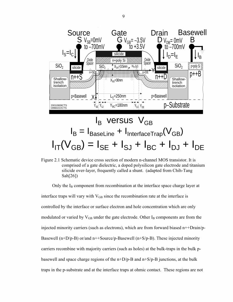
The discussion in this analytical theory chapter will follow the schematic cross-
sectional view of modern n-channel MOS transistor shown in Figure 2.1. The important
physical features of the nMOS include the n-type heavily doped high-conductivity
ploysilicon gate (n++G), the refractory metal silicide gate on n++G and the heavily doped
very-high-conductivity n-type drain and source extension (n++D and n++S), the medium-
highly doped high-conductivity n-type drain and source extension regions (n+SER and
n+DER), the p-type basewell channel region (p-BCR), the drain and source oxide
spacers, and the shallow-trench oxide isolation.
Electron-hole recombination can occur at the SiO2/Si interface traps located in the
five regions along surface channel: (1) the basewell-surface channel region (BCR), (2)
the source-junction space-charge region (SJR), (3) the drain-junction space-charge region
(DJR), (4) source extension region (DER) and (5) drain extension region (DER). This
study will focus on basewell-surface channel region and the results are also applicable to
the other regions.
9
HAL
O
HALO
**
19960222CTS20010909CTS
silicide
IB versus VGB
Shallow-trenchisolation
X
p++Bp+poly Sisilicide
YBC=180nm
n++Dsilicide
Shallow-trenchisolation
SiO2
n+DEn+SE Y
XSS=30nm
NIT(y)
IB = IBaseLine + IInterfaceTrap(VGB)
IIT(VGB) = ISE + ISJ + IBC + IDJ + IDE
n++S
YSJ YDJ
LG=250nmp+Basewell p+Basewell
YSE YDE p−Substrate
XOX=3.5nm
n+poly SiSiO2SiO2
SpacerOxide
SpacerOxide
Source
ID=IE IBIS=IC
VGB= −3.5VVSB=0mV VDB= 0mVSGate
GDrain
DBasewell
Bto +3.5V to −700mVto −700mV
Figure 2.1 Schematic device cross section of modern n-channel MOS transistor. It is comprised of a gate dielectric, a doped polysilicon gate electrode and titanium silicide over-layer, frequently called a shunt. (adapted from Chih-Tang Sah[26])
Only the IB component from recombination at the interface space charge layer at
interface traps will vary with VGB since the recombination rate at the interface is
controlled by the interface or surface electron and hole concentration which are only
modulated or varied by VGB under the gate electrode. Other IB components are from the
injected minority carriers (such as electrons), which are from forward biased n++Drain/p-
Basewell (n+D/p-B) or/and n++Source/p-Basewell (n+S/p-B). These injected minority
carriers recombine with majority carriers (such as holes) at the bulk-traps in the bulk p-
basewell and space charge regions of the n+D/p-B and n+S/p-B junctions, at the bulk
traps in the p-substrate and at the interface traps at ohmic contact. These regions are not
10
covered by the gate-conductor. Thus, the recombination rate or current don’t vary with
the gate voltage. It is the IB baseline.
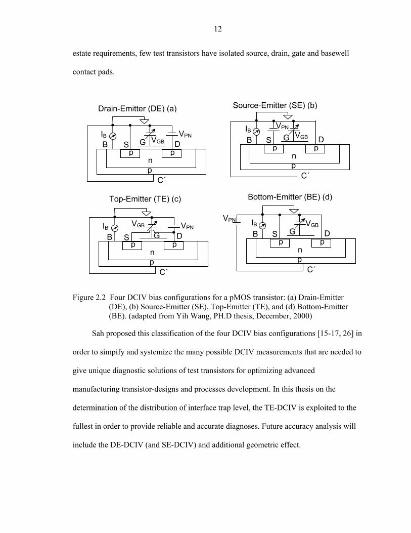
Recombination DCIV measurement on MOS transistors can use four different bias
configurations to inject minority carriers to the SiO2/Si interface [8, 15-17, 26], as
illustrated in Figure 2.2. These four configurations can be grouped in accordance with the
two traditional BJT geometries, the vertical BJT (VBJT) and lateral BJT (LBJT). For the
LBJT, given in Figures 2.2 (a) and (b), they are called the Drain-Emitter configuration
(DE-DCIV) and Source-Emitter configuration (SE-DCIV). For the VBJT, given in
Figures 2.2 (c) and (d), the drain and source p/n or n/p junctions are simultaneously
forward DC biased to the same terminal voltage, which is known as the Top Emitter
configuration or TE-DCIV. The other VBJT configuration is to forward bias the bottom
p/n junction of the p/n-junction basewell, which is known as the Bottom Emitter
configuration or BE-DCIV. The p/n junctions not forward biased are zero-biased, though
they can also be reverse-biased or even forward-biased at a lower voltage in each of the
bias configurations.
These four DC-bias configurations can provide high sensitivity and resolution to
monitor the dopant-impurity and interface trap concentration profiles and as well as the
electrical length of the five regions (SER, SJR, BCR, DJR and DER) and other transistor
design parameters, such as the gate/source, gate/base, and gate/drain oxide thickness, and
the series drain and source resistances [15-17]. All of these are increasingly difficult to
measure accurately and with confidence by traditional MOS transistor and metallurgical-
optical methods as the transistor shrinks due to the fundamental microscopic limitations.
11
Each of the configurations, in Figures 2.2 (a)-(d), provides a different and desired
BJT injection pathway and spatial distribution of minority at the SiO2/Si interface to help
further delineate the spatial distribution of the impurities and interface traps.
The boron acceptor has a liquid/solid segregation coefficient of 0.8, which gives
only about 20% variation of boron-concentration over the crystal length, while
phosphorus donor segregation coefficient is 0.35 and phosphorus sources have very high
vapor pressures to make the continuous-dopant during growth difficult to control. Thus,
all silicon integrated circuits start with a p-type high-resistance, 50 to 100 Ω cm p-type 8"
or 12" diameter silicon wafer for high-yield reason since 8" –by-several-foot silicon
single crystals can be grown nearly defect-free, dopant-impurity-free and oxygen-free
(using float-zone in vacuum chamber). Therefore, only the pMOST in digital circuits
manufactured on high-resistivity p-Si wafers has an n-base/p-collector-substrate n/p
junction basewell for transistor isolation which can be used in the BE-DCIV
methodology. The n-B/p-C (p-collector) junction well is formed by ion-implantation.
It is not available for the digital nMOST which has a boron ion-implanted p-B/p-C
high/low junction basewell. However, both nMOST and pMOST can be measured in the
BE-DCIV bias configuration on analog test transistor wafers since the higher-gain or
high-transconductance nMOST requires a p-B/n-C junction basewell for electrical
isolation.
For the two lateral BJT or LBJT configurations, the DE-DCIV is the most
commonly used due to the ganged base pad and source pad. These ganged pads come
from test transistor patterns with many channel lengths and widths. Due to large real
12
estate requirements, few test transistors have isolated source, drain, gate and basewell
contact pads.
Figure 2.2 Four DCIV bias configurations for a pMOS transistor: (a) Drain-Emitter (DE), (b) Source-Emitter (SE), Top-Emitter (TE), and (d) Bottom-Emitter (BE). (adapted from Yih Wang, PH.D thesis, December, 2000)
Sah proposed this classification of the four DCIV bias configurations [15-17, 26] in
order to simpify and systemize the many possible DCIV measurements that are needed to
give unique diagnostic solutions of test transistors for optimizing advanced
manufacturing transistor-designs and processes development. In this thesis on the
determination of the distribution of interface trap level, the TE-DCIV is exploited to the
fullest in order to provide reliable and accurate diagnoses. Future accuracy analysis will
include the DE-DCIV (and SE-DCIV) and additional geometric effect.
p pn p
DS G
C΄
VPNVGB p p
n p
D S G
C΄
VPN VGB IB IB
p pn p
DS G
C΄
VPNVGB IB
B B
B p p n p
D S G
C΄
VGB IBB
VPN
Top-Emitter (TE) (c) Bottom-Emitter (BE) (d)
Source-Emitter (SE) (b) Drain-Emitter (DE) (a)

13
2.3 Theory of R-DCIV Methodology
The dimensions of Metal-Oxide-Silicon (MOS) field-effect transistors have
continued to decrease, projected by SIA [4] in 1999 to drop below 100nm around the end
of decade and has done so [2]. The width to length ration, W/L, could be unity or even
smaller, making the width effect as important as the length effect on the transistor
electrical characteristics. In this case, the transistor is three-dimensional (3D). If a MOS
transistor is much wider than its length, the structure is nearly two-dimensional (2D) as
indicated by the cross-sectional view shown in Figure 2.1.
The traditional industrial practice to design a transistor has been the use of super-
computers to obtain the DC steady-state numerical solutions of the three-dimensional
(3D) structure via the finite-different method. The 3D electrical characteristic solutions
are tedious and complicated since they include the five simultaneous nonlinear partial
Shockley equations, which govern the diffusion, drift and generation-recombination-
trapping of electrons and holes [6, pp. 268, Eqs (350.1)-(350.6)]. As a diagnostic
methodology, it is untenable to experimentally verify the transistor design during the
engineering phase and manufacturing since the numerical solution takes a huge amount
of time to reach an optimum transistor design. The dependence of the nonlinear
coefficients (mobility, diffusivity, generation-recombination-trapping rates) on the
solutions ( the electric field and potential, and the electron and hole concentrations) is not
precisely known and can only be approximated by highly simplified quantum and
statistical mechanical theory to give tractable analytical formulas.
The further simplified empirical formulas have been used in common engineering
practice for the fundamental parameters, which make the model and methodology
inapplicable as an extrapolation scheme. Here, we use the partitioning methodology to
14
divide the three-dimensional (3D) transistor structure into one-dimension (1D),
disregarding the coupling effects of the other two dimensions (such as lateral diffusion
and drift of the electrons and holes), because the salient feature of the DCIV
methodology is that some of the 1D features in the DCIV characteristics are strictly
independent of the lateral (or y-axis) variation.
Compared with the channel length (y-axis), the thickness of surface space-charge
layer and gate oxide is very thin. Thus, the variation of electric potential and field is small
in the y-axis compared their x-variation, i.e., EY(x,y) << EX(x,y), which allows us to
solve the 1D x-variations exactly using 1D MOS Capacitor (MOSC) and to sum these
adjacent (in y-direction) to give the 2D solution such as the DC current of the basewell
terminal.
In the R-DCIV measurements, excess minority carriers are injected by a forward-
biased p/n junction into the SiO2/Si interface which covers channel region between the
source and drain of MOS transistors: the basewell channel region (BCR) and the drain
and source junction and extension regions (DJR, SJR, DER and SER). The peaked-
components in a IB-VGB plot arise from electron-hole recombination at the SiO2/Si
interface traps, NIT (No./cm2), in the five gate-covered regions along the interface
channel. The surface recombination rate and current of each region reach their maximum
when the gate voltage is varied to make the local surface concentration of electrons and
holes nearly equal. When the bias configurations contain one or more forward-biased p/n
junctions, the device structure becomes a lateral or vertical bipolar junction transistor
(LBJT and VBJT). Since LBJT is always available in a MOS transistor, the R-DCIV
15
measurement method can be applicable to actual small MOS transistors used in the
integrated circuit [16].
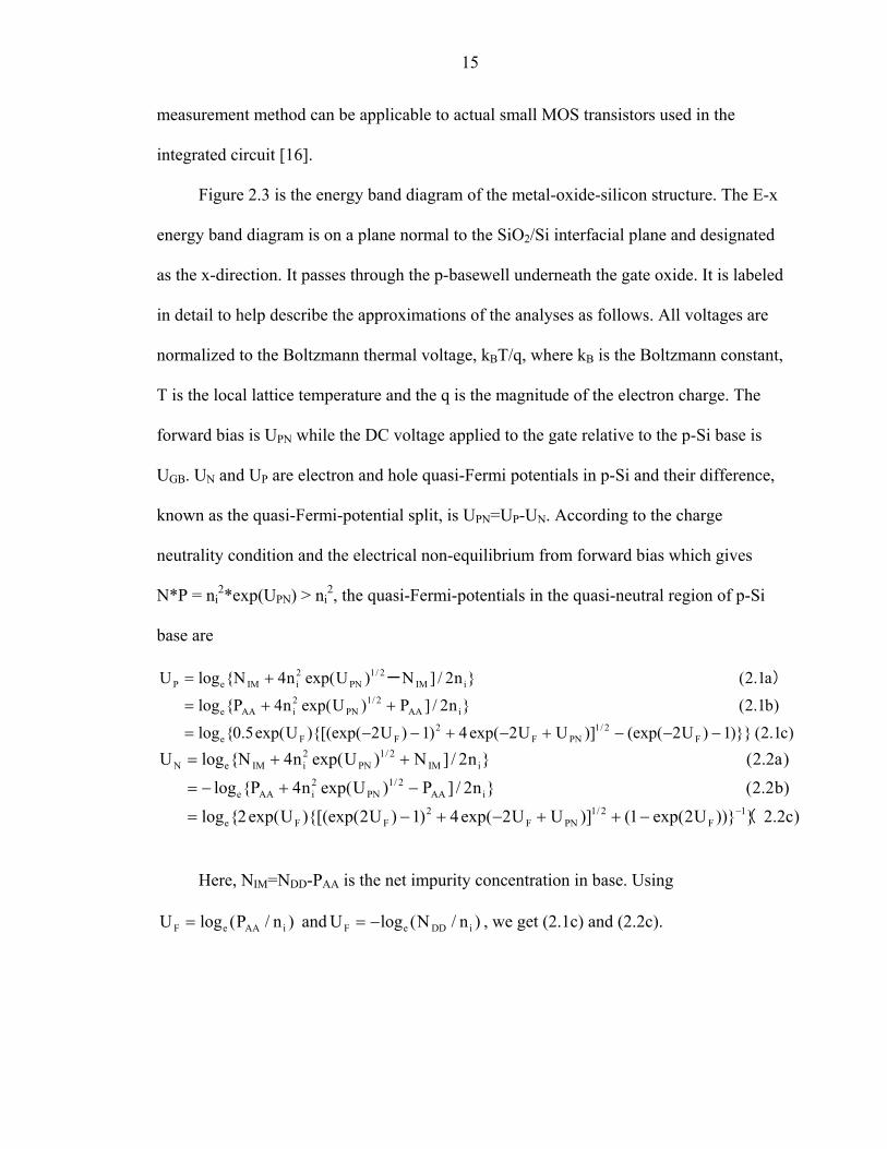
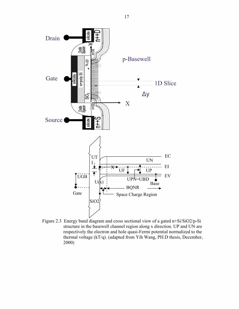
Figure 2.3 is the energy band diagram of the metal-oxide-silicon structure. The E-x
energy band diagram is on a plane normal to the SiO2/Si interfacial plane and designated
as the x-direction. It passes through the p-basewell underneath the gate oxide. It is labeled
in detail to help describe the approximations of the analyses as follows. All voltages are
normalized to the Boltzmann thermal voltage, kBT/q, where kB is the Boltzmann constant,
T is the local lattice temperature and the q is the magnitude of the electron charge. The
forward bias is UPN while the DC voltage applied to the gate relative to the p-Si base is
UGB. UN and UP are electron and hole quasi-Fermi potentials in p-Si and their difference,
known as the quasi-Fermi-potential split, is UPN=UP-UN. According to the charge
neutrality condition and the electrical non-equilibrium from forward bias which gives
N*P = ni2*exp(UPN) > ni
2, the quasi-Fermi-potentials in the quasi-neutral region of p-Si
base are
)c1.2()1)U2(exp()]UU2exp(4)1)U2)[(exp(Uexp(5.0log
)b1.2(n2/]P)Uexp(n4Plog
a1.2(n2/]N)Uexp(n4NlogU
F2/1
PNF2
FFe
iAA2/1
PN2iAAe
iIM2/1
PN2iIMeP
−−−+−+−−=
++=
+= )-
)c2.2))U2exp(1()]UU2exp(4)1)U2)[(exp(Uexp(2log
)b2.2(n2/]P)Uexp(n4Plog
)a2.2(n2/]N)Uexp(n4NlogU
1F
2/1PNF
2FFe
iAA2/1
PN2iAAe
iIM2/1
PN2iIMeN
(−−++−+−=
−+−=
++=
Here, NIM=NDD-PAA is the net impurity concentration in base. Using
)n/P(logU iAAeF = and )n/N(logU iDDeF −= , we get (2.1c) and (2.2c).
16
The total energy band bending is denoted by the surface potential US. The electron
and hole concentrations at the SiO2/Si interface (NS and PS) are modulated by the gate
voltage via bending the Si energy band:
)3.2()UUexp(n)y,0x(PP SPiS −===
)4.2()UUexp(n)y,0x(NN NSiS −===
In our analysis, the surface potential normalized to the thermal voltage, kT/q, is the
intrinsic position of the Fermi Potential Level at the surface or SiO2/Si interface.
)5.2(kT/qVU)y,0x(U SSI =≡=
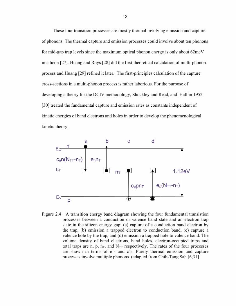
Four fundamental electron-hole transition processes,between the continuous band
states of silicon crystal and the localized trap states with an energy level ET in the silicon
gap, can be illustrated using the energy band diagram as shown in figure 2.4. The rate
(event/second-cm3) of the four processes can be conveniently described by: (a) electron
capture from the conduction band at cn(NTT-nT), (b) electron emission to the conduction
band at ennT, (c) hole capture from the valence band at cpnT, and (d) hole emission to the
valence band at ep(NTT-nT). Here, n and p are electron and hole concentrations in the
conduction band and valence band respectively, NTT is the total density (#/cm3) and nT is
the electron-occupied density of the trap states (#/cm3), and e’s (sec-1) and c’s (cm3sec-1)
are emission and capture rate coefficients of the four processes which depend on the
energy levels of both the trap state and the band state.
17
Figure 2.3 Energy band diagram and cross sectional view of a gated n+Si/SiO2/p-Si
structure in the basewell channel region along x direction. UP and UN are respectively the electron and hole quasi-Fermi potential normalized to the thermal voltage (kT/q). (adapted from Yih Wang, PH.D thesis, December, 2000)
Drain
Gate
Source
X Δy
1D Slice
p-Basewell
UGB U(x)
EC
EI
EV
UN
UP X
Base
UF
Space Charge Region
UPN=UBD
Gate
UTI
SiO2
BQNR
18
These four transition processes are mostly thermal involving emission and capture
of phonons. The thermal capture and emission processes could involve about ten phonons
for mid-gap trap levels since the maximum optical phonon energy is only about 62meV
in silicon [27]. Huang and Rhys [28] did the first theoretical calculation of multi-phonon
process and Huang [29] refined it later. The first-principles calculation of the capture
cross-sections in a multi-phonon process is rather laborious. For the purpose of
developing a theory for the DCIV methodology, Shockley and Read, and Hall in 1952
[30] treated the fundamental capture and emission rates as constants independent of
kinetic energies of band electrons and holes in order to develop the phenomenological
kinetic theory.
Figure 2.4 A transition energy band diagram showing the four fundamental transistion processes between a conduction or valence band state and an electron trap state in the silicon energy gap: (a) capture of a conduction band electron by the trap, (b) emission a trapped electron to conduction band, (c) capture a valence hole by the trap, and (d) emission a trapped hole to valence band. The volume density of band electrons, band holes, electron-occupied traps and total traps are n, p, nT, and NTT respectively. The rates of the four processes are shown in terms of e’s and c’s. Purely thermal emission and capture processes involve multiple phonons. (adapted from Chih-Tang Sah [6,31].
EC
EV
ET
n
p
a b c d
nT
cnn(NTT-nT) ennT
cppnT ep(NTT-nT)
1.12eV
19
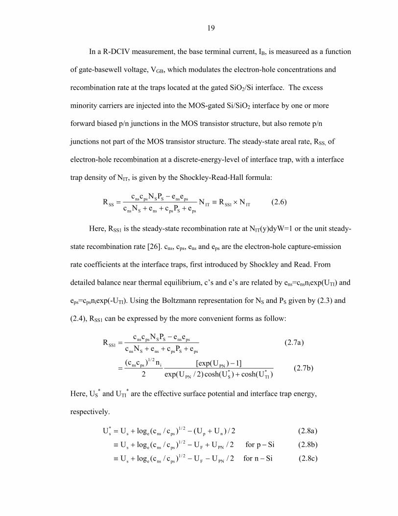
In a R-DCIV measurement, the base terminal current, IB, is measureed as a function
of gate-basewell voltage, VGB, which modulates the electron-hole concentrations and
recombination rate at the traps located at the gated SiO2/Si interface. The excess
minority carriers are injected into the MOS-gated Si/SiO2 interface by one or more
forward biased p/n junctions in the MOS transistor structure, but also remote p/n
junctions not part of the MOS transistor structure. The steady-state areal rate, RSS, of
electron-hole recombination at a discrete-energy-level of interface trap, with a interface
trap density of NIT, is given by the Shockley-Read-Hall formula:
)6.2(NRNePceNc
eePNccR IT1SSIT
psSpsnsSns
psnsSSpsnsSS ×≡
+++−
=
Here, RSS1 is the steady-state recombination rate at NIT(y)dyW=1 or the unit steady-
state recombination rate [26]. cns, cps, ens and eps are the electron-hole capture-emission
rate coefficients at the interface traps, first introduced by Shockley and Read. From
detailed balance near thermal equilibrium, c’s and e’s are related by ens=cnsniexp(UTI) and
eps=cpsniexp(-UTI). Using the Boltzmann representation for NS and PS given by (2.3) and
(2.4), RSS1 can be expressed by the more convenient forms as follow:
)b7.2()Ucosh()Ucosh()2/Uexp(
]1)U[exp(2
n)cc(
)a7.2(ePceNc
eePNccR
*TI
*SPN
PNi2/1
psns
psSpsnsSns
psnsSSpsns1SS
+−
=
+++−
=
Here, US* and UTI
* are the effective surface potential and interface trap energy,
respectively.
)c8.2(Sinfor2/UU)c/c(logU
)b8.2(Sipfor2/UU)c/c(logU
)a8.2(2/)UU()c/c(logUU
PNF2/1
psnses
PNF2/1
psnses
np2/1
psnses*s
−−−+≡
−+−+≡
+−+=
20
)9.2()]c/cln(21Tk/)EE[(Tk/EU psnsBITB
*TI
*TI +−==
Here, UTI is the interface trap energy level, measured from the intrinsic Fermi level EI,
defined by UTI = -(ET-EI)/q. US(y) = UI(x=0,y), commonly known as the surface energy
band bending in the basewell channel region, is the total change of the electric potential
along the x-axis at a particular y-position from the SiO2/Si interface (x=0) to the interior.
UI(x=infinity, y) = 0 is taken as the reference). The expression of (2.7) is exact with no
approximations other than the thermal Boltzmann distribution with lattice temperature T.
It immediately shows the presence of a peak at US*=0 or cnsNS=cpsPS when the surface
potential, US, or the gate voltage VGB is varied.
)b02.1(]1)2/U[exp(2
n)cc(
)a10.2()Ucosh()2/Uexp(
]1)U[exp(2
n)cc(R
PNi
2/1psns
*TIPN
PNi2/1
psnspeak1SS
−=
+−
=−
For an interface trap energy level at around mid-gap with UTI*=0, we will have the
classic IB∝exp(qV/2kT) dependence, shown in (2.10b). This dependence suggests that
many of the observed n=2 non-ideal IV characteristics of p/n junctions [1, 7, 8, 31] could
be due to interface traps at the surface perimeter of the p/n junction rather than residual
bulk traps in the bulk space-charge-layer of the p/n junction.
RSS1 has a peak when the steady-state capture rate of electrons and holes are equal.
It is expected from the equality of the four transitions, electron and hole capture and
emission transitions at the trap. But more important, it is an immensely useful result that
provides the simplest basis for qualitative interpretation and understanding of
experimental data. The peak amplitude increases exponentially with forward bias, UPN,
21
which gives the tremendous sensitivity and hence spatial resolution that are unique
features of the DCIV method. The surface potential at the peak current (US*=0) is
)c11.2(Sinfor2/UU)c/c(log
)b11.2(Sipfor2/UU)c/c(log
)a11.2(2/)UU()c/c(logU
PNF2/1
psnse
PNF2/1
psnse
np2/1
psnsepeakS
−++−≡
−−+−≡
++−=−
The peak formula (2.11a) was derived by Sah-Noyce-Shockley in 1957 [31] and used by
Cai and Sah in 2000 for DCIV theory [20].
The basewell recombination current (IB-BCR) [7, 8, 20, 26] is obtained by integrating
the SRH steady-state electron-hole recombination rate at the interface over the channel
area dydz:
)b12.2(dy)y(N)Ucosh())y(Ucosh()2/)y(Uexp(
]1))y(U[exp(2
Wn)cc(q
)a12.2(dydz)y(N)y,V(Rq)V(I
IT*TI
*sPN
PNi2/1
psns
ITGB1SSGBB
∫
∫∫
+−
=
=
For low injection levels, traditionally defined as N < PAA/10 in p-Si, we have
UP≈UF>0 for p-Si and UN≈UF<0 for n-Si, where UF is the majority carrier Fermi
potential. This is the common application range of the DCIV methodology. According to
(2.11b) and (2.11c), the RSS1-peak lies in the flat-band to the intrinsic gate voltage range
(0<US<UF, for p-Si). Using the Sah’s exact formula [5, pp.129]:
VS = VGB - VFB - 2•sign(VS)•VAA[1 + (VGB - VFB - kT∆D/q)/VAA]1/2 - 1 (2.13)
We have an approximation in this flat-band/intrinsic range,
VGB = VFB + VS + 2(VAA)1/2(VS)1/2 ( )2.14a
= VFB + VS + 0.053(XOX/1nm)(PAA/1017cm-3)1/2 (2.14b)
Then, the gate voltage at peak current IB-peak is
22
)15.2()V()cm10
p)(nm1
X(053.0VVV 2/1peakS
2/1317
AAOXpeakSFBpeakGB −−−− ++=
Here, VAA = εSqPAA/2COX2 = 0.695*10-3*(XOX/1nm)(PAA/1017cm-3)1/2. VFB is the flat-
band voltage which contains Si-Gate/SiO2/Si work function difference and the oxide
charge from the charged electron and hole traps inside the thin oxide film, QOX/COX,
where COX= εS/XOX is the oxide capacitance per unite area. The last term in (2.13), (2.14)
and (2.15) is the voltage drop across the oxide layer.
The gate voltage at peak current VGB-peak is determined by the three terms: VFB, VS-
peak and VAA, as indicated by (2.15) and (2.11). The dependencies on the transistor design
parameters are (1) the substrate dopant concentration, (2) gate oxide thickness through
VAA, (3) the ratio of electron and hole capture rates, (4) the flat-band voltage VFB and (5)
the emitter junction forward bias VPN. As a result, the IB-peak will shift toward a more
positive VGB for a higher substrate impurity concentration or a thicker oxide thickness at
a given forward-bias-voltage VPN in an nMOS transistor.
The theoretical variation of RSS1-VGB lineshape due to device parameters is
examined below, using the formula of half-width at half maximum (HWHM) at low
injection levels [20]:
)b16.2()siderinsic(int]VVV[V2VV
)a16.2()sideflatband(]VVV[V2VV
peakSSpeakSAASGB
SpeakSpeakSAASGB
−−∆++∆=∆
−∆−−+∆=∆
−−−
−−+
As indicated in (2.16a) and (2.16b), the half-width on the flat-band accumulation side of
the peak is always larger and broader than that on the intrinsic-inversion side of the peak.
Thus, the recombination current lineshape is fundamentally asymmetric. A higher surface

23
impurity concentration and thicker oxide will each give a larger HWHM or broader
lineshape.
For low injection levels, injected minority concentration has negligible effect on
surface band bending, since VS-VGB curve is mainly determined by the concentration of
the majority carriers and ionized impurity atoms in the substrate. Therefore, effect of
forward bias VPN at low injection level will have a negligible effect on DCIV lineshape.
At high injection levels with N>10×PAA, we have UP≈-UN or the electron and hole
concentrations in the channel region are nearly equal, and the maximum surface
recombination rate is near the flat-band. The exact result is US-peak = loge(cps/cns)1/2 which
can be derived from (2.11a).
As shown in (2.12b), the IB versus VGB lineshape is affected by US* via the
cosh(US*) term in the denominator, assuming a single-level interface trap at the mid-gap,
ETI*=0. Interface trap concentration NIT in the numerator of (2.12) only alters the peak
amplitude but not the lineshape. Consequently, lineshape of IB–VGB curve will be
determined by the dopant impurity concentration and oxide thickness.
2.4 Theoretical Computations for Confident Level
Before an attempt can be made to obtain the confident level of BI by comparing
with the FD exact solutions when using the R-DCIV methodology, a phenomenological
model must be created and its analytical solutions derived. It is well known that the more
exact the model is, the more accurate the derived solution will be. However, the solution
will become complex with the advantage of model exactness, which will become quite
clear in this thesis.

24
In a semiconductor, temperature has an enormous influence on the electrical
properties, especially the conductivity. The dielectric constants of silicon and silicon
oxide have slight temperature dependence. A formula for SiO2/Si is not available since
structural effects may begin to play an important role for thin oxides, and the formula
would become a function of temperature and thickness. In this thesis, εSiO2=3.90. For thin
oxides transistors, the effective dielectric constant may be different due to interfacial
layers. In fact, the concept of dielectric constants becomes debatable when only a few
layers of atoms are involved.
Increasing temperatures are associated with a narrowing of the energy gap. A
second-order polynomial by Bludau, Onton and Heinke [32] has been modeled to cover
temperature range from 0 to 300K from the data on the absorption coefficient of highly
pure p-type silicon. Sah, McNutt and Chan [33] gave the formula when temperature is
above 300K and less than 500K. Since the intrinsic carrier concentration is an
exponential-like function of the energy gap, it is important to have an accurate value for
the energy gap. Otherwise, the result will be substantially inaccurate.
The calculated values of the energy gap and measures values of the intrinsic carrier
concentration by Sah, McNutt and Chan [33], can use to compute the memh product. One
remaining problem is the requirement of the individual effective masses to calculate NC
and NV. Since there is no way to unequivocally separate the effective masses at
temperatures significantly above 4.2K, this thesis uses the 4.2K data, obtained from
cyclotron resonance measurements, which gave me/mo=1.065 and mh/mo=0.647, for an
me/mh ratio of 1.646.
25
The Boltzmann distribution (exponential) is a well-known method used in the non-
degenerate case, i.e. low carrier concentration <~1018cm-3, best approximating the Fermi
statistics integral at low temperatures and/or low impurity doping, when (EC-EF)/kT>4 or
EF>EC-4kT. Degeneracy or Fermi statistics is used to deal with high carrier
concentrations. Degeneracy is always important when the carrier concentration is high
(and not just the dopant), such as in the presence of a highly forward biased p/n junction
or under a bright light. In particular, degeneracy is important in the inversion and
accumulation regions along the SiO2/Si interface channel of MOS transistors.
Nevertheless, degeneracy is still generally not taken into account due to the complexity.
There is no analytical solution for the Fermi statistics integral, so either full-range
analytical approximations must be used, such as those shown in Blackemore’s paper on
the subject of F-D integrals [34], or iterative solutions must be employed, such as the
rational Chebyshev approximations [35] used in this thesis.
It is reasonably accurate to assume that all dopant impurities are ionized in most
conditions. As long as shallow-level dopants are used, which is equivalent to saying that
the binding energy for electron (n-type) or hole (p-type) is small, so that almost complete
ionization is expected. In p-type material, this can be easily rationalized by considering
the Fermi level with respect to the dopant impurity level: as long as the Fermi level is
above the acceptor level, the level should be filled with an electron and unoccupied by a
hole, and hence the acceptors will be completely ionized. Similarly, as long as the Fermi
level lies below the donor level in an n-type sample, the probability of the level being
filled is low, and hence, the donor is likely ionized. When temperature is very low and
the material is heavily doped, and/or the impurity level is deep, the impurity may not
26
ionize completely, which is what is called deionization. This can be made sense
physically at low temperatures: if there is not enough thermal energy to release the
electrons or holes, then the impurities will not be ionized, or an electron will be trapped at
the donor and hole will be trapped at the acceptor. For high doping concentrations, the
Fermi level can go above donor level or below the acceptor level, and the fraction of
ionized impurities will be consequently decrease. For electron-hole recombination current
at the SiO2/Si interface traps, gate voltage would attract electrons to interface and push
holes away from interface in accumulation region. Thus, some donor impurities atoms
near the SiO2/Si interface are occupied by the electrons and are deionized. The acceptor
impurities are still ionized. In inversion region, gate voltage will push electrons away
from interface and attract holes to interface. Thus, donor impurities are still ionized and
acceptor impurities trap the holes at interface and are deionized. In this thesis, we only
consider non-compensated materials, i.e. PAA=0 in n-Base and NDD=0 in p-Base. Thus
deionization is entirely negligible except in the strong accumulation range.
For modern ULSI technology, polysilicon gates are universally used on MOS
devices. Gate depletion is possible and potentially non-negligible for lowly doped gates
(<5×1020cm-3). Polysilicon gates have some tremendous processing and transistor density
benefits over metal gates, and can withstand high temperature steps that would cause
most deposited metal gates to evaporate, particularly the source/drain drive-in step. As
oxide thickness continues to decrease, polysilicon depletion becomes a more important
problem. The addition of the polysilicon depletion increases calculation complexity
substantially since it introduces a second surface potential for the polysilicon gate. Yaron
and Frohman-Bentchkowsky [36], as well as Sah [5] have shown how to include the
27
polysilicon depletion effect in CV theory. In this thesis, the confidence levels are
computed for both metal and silicon gates.
The most important effects are included in modeling R-DCIV characteristics of a
MOS transistor. However, there are many factors which are to be assumed negligible, but
we should mention them for completeness. The transition layer between Si and SiO2 is
not abrupt an on the order of about one or two atomic layers (~6A) in thin oxide [37-39].
The transitional layer of SiOX has a different dielectric constant. The dielectric change in
this very thin region should not be drastic enough to effect DCIV curves significantly,
thus this effect was not included in this thesis. Energy gap narrowing was ignored for
very high impurity concentrations. There is much debate about the modeling of the
energy gap narrowing as a function of doping, and it is questionable whether the
formulae are independent of deionization and especially impurity banding. Fringe field
effects as well as frequency dependency of the dielectrics were not included. Series
resistance, which is simple to include, was omitted since the R-DCIV current density is
low. Also, impurity banding was ignored in the analysis.
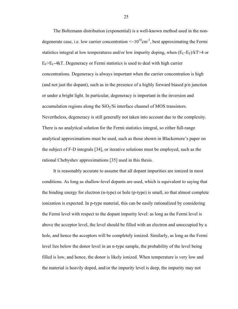
The charge density in the semiconductor is given the equation
)1.4.2()nPNPN(q TDA −+−+−ρ=
Here, N and P are electron and hole concentrations, respectively. The nT terms
represents the contribution from trapped charge. NA and PD are respectively the ionized
acceptors and donors [6,30].
)b2.4.2()kT/]EEexp([g1
NN
)a2.4.2()kT/]EEexp([g1
PN
DFA
DDD
FAA
AAA
−+=
−+=
28
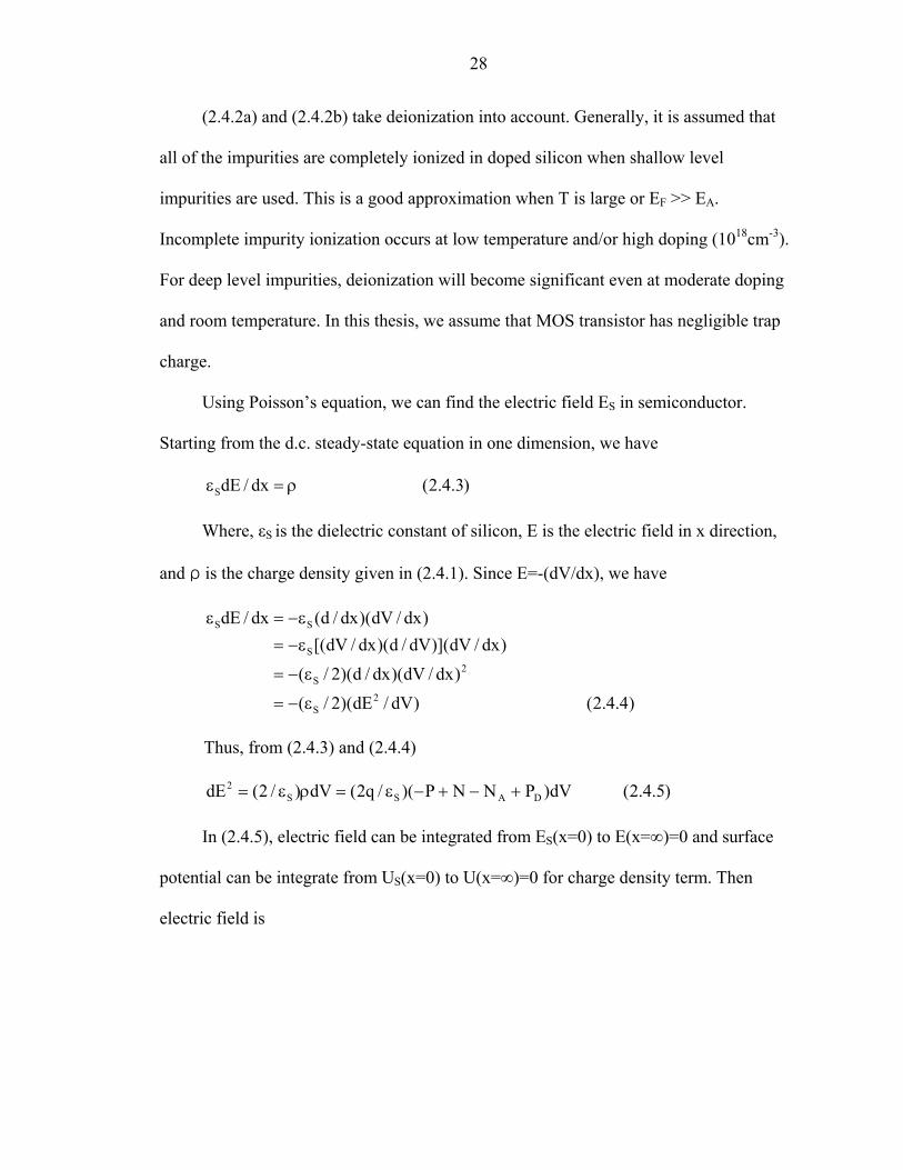
(2.4.2a) and (2.4.2b) take deionization into account. Generally, it is assumed that
all of the impurities are completely ionized in doped silicon when shallow level
impurities are used. This is a good approximation when T is large or EF >> EA.
Incomplete impurity ionization occurs at low temperature and/or high doping (1018cm-3).
For deep level impurities, deionization will become significant even at moderate doping
and room temperature. In this thesis, we assume that MOS transistor has negligible trap
charge.
Using Poisson’s equation, we can find the electric field ES in semiconductor.
Starting from the d.c. steady-state equation in one dimension, we have
)3.4.2(dx/dES ρ=ε
Where, εS is the dielectric constant of silicon, E is the electric field in x direction,
and ρ is the charge density given in (2.4.1). Since E=-(dV/dx), we have
)4.4.2()dV/dE)(2/(
)dx/dV)(dx/d)(2/(
)dx/dV)](dV/d)(dx/dV[()dx/dV)(dx/d(dx/dE
2S
2S
S
SS
ε−=
ε−=
ε−=ε−=ε
Thus, from (2.4.3) and (2.4.4)
)5.4.2(dV)PNNP)(/q2(dV)/2(dE DASS2 +−+−ε=ρε=
In (2.4.5), electric field can be integrated from ES(x=0) to E(x=∞)=0 and surface
potential can be integrate from US(x=0) to U(x=∞)=0 for charge density term. Then
electric field is

29
)6.4.2()])UUexp(g1
)UUUexp(g1logU[N
)])UUexp(g1
)UUUexp(g1logU[N
)]UU(F)UUU(F[N
)]UU(F)UUU(F[NkT2E
FDA
SFDDeSDD
AFA
SAFAeSAA
FC2/3FCS2/3C
FV2/3FVS2/3VS
2S
−++−+
+−
−+−−+
+
−−−++
+−−+−−ε
=
+
+
The surface potential, US, represents the amount of band bending of the silicon
band at the SiO2/Si interface caused by the applied electric field or gate voltage. In this
thesis, we only discuss the non-compensated region, i.e., either donor or acceptor is the
dopant in substrate of MOS transistor.
2.4.1 BI, BD and FI Approximations Compared with FD Exact Theory
Before finding the confident level of on % deviation the BI approximation, we first
compare BI, BD and FI approximations with FD exact theory using R-DCIV
methodology. Here, BI stands for Boltzmann distribution of electrons and holes in energy
and impurity full ionization. BD stands for Boltzmann distribution and impurity
Deionization. FI stands for Fermi distribution of electrons and holes and impurity full
ionization. FD stands for Fermi distribution and impurity deionization.
For modeling R-DCIV curves, the BI approximation is the fastest solution. There
are two ways to derive the BI solution. One would be to build a BI model from the start
using the Boltzmann (exponential) distribution for the carrier concentration while
ignoring the effects of deionization completely. This is the typical textbook approach. A
somewhat more instructive method is to present one complete derivation for the exact
case (the degenerate and deionized model) and then reduce to a simper case. The later
approach will be used in this thesis.
30
The Boltzmann ionized solution is most useful just after the onset of accumulation
or inversion at temperatures higher than 250K and doping less than 1018cm-3. When in the
strong accumulation or inversion ranges, Fermi statistical distribution are required. At
low temperatures and/or high doping, the effect of deionization becomes non-negligible
and should be included. However, temperature at around 300K and impurity
concentration lower than1018cm-3 are in the practical ranges. In addition, BI
approximation solution is simple and time-saving. These were the right reasons we used
BI approximation when using DCIV methodology to extrapolate the profile of impurity
concentration, interface trap concentration and oxide thickness [26, 40].
The exact FD solution for a p-doped semiconductor is given by [5, pp.129]:
)7.4.2(C/E)V(signVVV OXSSSSFBGB ε++=
According to (2.4.6), the electric field at the surface p-Si, which includes the electrical
non-equilibrium from the forward applied p/n junction voltage VPN, is given by
)8.4.2(FDfor]))UUexp(g1
)UUUexp(g1[logU(P
)]UUU(F)UUUU(F[N
)]UU(F)UUU(F[NkT2E
AFA
SAFAeSAA
PNFC2/3PNFCS2/3C
FV2/3FVS2/3VS
2S
−+−−+
++
+−−+−++
+−−+−−ε
=
Once we assume that all the dopant impurities are fully ionized, the logarithmic tem of
(2.4.8) is dropped, we have the electric field of FI
)9.4.2(FIforUP)]UUU(F)UUUU(F[N
)]UU(F)UUU(F[NkT2E
SAA
PNFC2/3PNFCS2/3C
FV2/3FVS2/3VS
2S
+−−−++
+−−+−−ε
=
++
Reducing this result to BD solution is straightforward. All the FD integrate are simply
replaced by exponentials, which is valid when Fermi energy less than about -4 [69].
31
)10.4.2(BDfor]))UUexp(g1
)UUUexp(g1[logU(P
)]UUUexp()UUUU[exp(N
)]UUexp()UUU(exp[NkT2E
AFA
SAFAeSAA
PNFCPNFCSC
FVFVSVS
2S
−+−−+
++
−−−++
+−−+−−ε
=
++
In order to remove the deionization effect, we assume the trap level is far away from the
Fermi level exp(UF-UA)<<1, which causes the logarithmic term of (2.4.8) to approach
zero. Thus, the electric field of BI is
)11.4.2(forBIUP)]UUUexp()UUUU[exp(N
)]UUexp()UUU(exp[NkT2E
SAA
PNFCPNFCSC
FVFVSVS
2S
+−−−++
+−−+−−ε
=
++
The different electric field form (BI, BD, FI and FD) give different surface potential US,
which would affect the lineshape of DCIV curves.
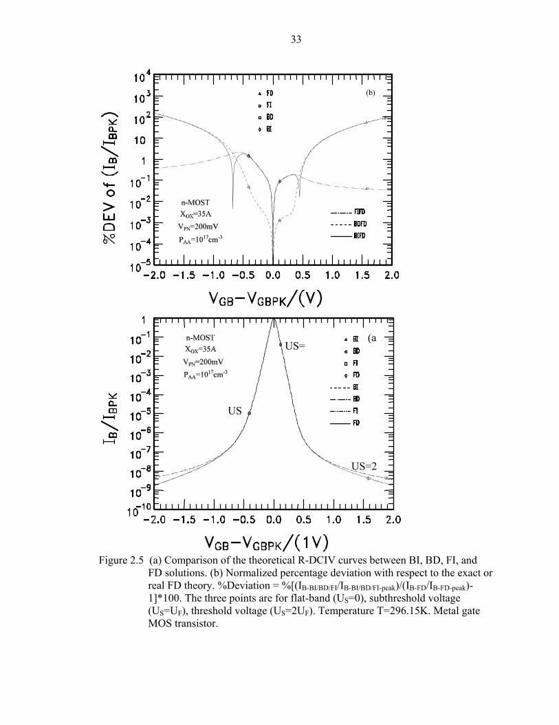
The four recombination DCIV curves are shown in Figure 2.5. The Lineshape of
the three approximations are almost the same as the exact Fermi-Deionization solution,
the difference between Fermi and Boltzmann statistics appears only when IB is around
eight decades smaller than peak current IB-peak. The difference between using fully
ionization and deionization models, such as BI and BD or FI and FD, is very small as
shown in Figure 2.5(a). From Figure 2.5(a), the 90 percent of the peak current covers a
gate voltage range from -0.10V to +0.10V. Figure 2.5(b) shows the % deviation is less
than 0.1% for all three approximations in this gate voltage range for peak current IB-peak
down to the 10% peak.
As shown in Figure 2.5, the switch from full ionization to deionization generally
results in very little gain by comparing with the increase in accuracy gained by switching
from Boltzmann to Fermi statistics. However, in situations where the temperature is very
32
low and/or the dopant concentration is quite high, deionization effects are non-negligible.
Also, if the dopant produces a deep-level trap, deionization will become significant factor
regardless of the doping concentration or temperature. According to Figure 2.5, we can
conclude that BI and FI solutions are respectively nearly as good as BD and FD solutions,
especially in accumulation region since deionization occurs only in this region.
The non-degenerate, fully-ionized solution is simplest when we assume that the
minority carrier terms are negligible and the majority surface concentration is much
larger than the bulk concentration, and the deionization term is dropped. This assumption
would invalidate the Boltzmann assumption in some case, such as in strong accumulation
region. But it allows us to find an analytical solution. For Fermi-Deionization case, the
final solution will be iterative, which is the main disadvantage of including degeneracy.
An exactly accurate numerical theoretical solution is impossible because of the
approximation the formulae used for the normal and inverse Fermi integrals.
The effects of deionization in the application range are generally so small that the
error from using Boltzmann statistics instead of Fermi will swamp any gain from
including deionization, except at the extremes, such as high doping and/or low
temperature at the onset of inversion or accumulation, or for deep level traps. The
inclusion of deionization also makes the Boltzmann case non-analytical. More important,
BI solution is simple and time-saving. For these reasons, we will compute the confident
level or percentage deviation of the BI solution by comparing with the exact FD theory.
33
Figure 2.5 (a) Comparison of the theoretical R-DCIV curves between BI, BD, FI, and
FD solutions. (b) Normalized percentage deviation with respect to the exact or real FD theory. %Deviation = %[(IB-BI/BD/FI/IB-BI/BD/FI-peak)/(IB-FD/IB-FD-peak)-1]*100. The three points are for flat-band (US=0), subthreshold voltage (US=UF), threshold voltage (US=2UF). Temperature T=296.15K. Metal gate MOS transistor.
(aUS=
US=2
US
(b)
34
Five important factors that affect IB–VGB lineshape are analyzed. These are
expected to be dominant in conventional or production MOS transistors. They are:
• Dopant Impurity Concentration Dependence • Oxide Thickness Dependence • Injected Minority Carrier Concentration Dependence • Energy Position of Discrete Energy Level Interface Traps • Temperature Dependence
A mid-gap symmetrical interface trap is assumed ET-EI=0with cns=cps=10-8cm-3/s,
and NIT=1010cm-3. The effect of ratio of electron and hole capture rates at the mid-gap on
the DCIV lineshape is small, which will be discussed in the chapter 3. ni=1010cm-3
corresponding to T=296.57K=23.42C=74.156F. The length and width of MOS transistors
are 10um and 1um, respectively. These results are the new applications that provide the
feedbacks for optimization of the design and fabrication of increasing smaller transistor
when using the simple and time-saving Boltzmann approximation with impurity full-
ionized solution of R-DCIV methodology.
2.4.2 Dopant Impurity Concentration Dependence
When the channel length of modern MOS transistor is scaled to 0.25um and below,
a much higher dopant impurity concentration is necessary to reduce the thickness of the
surface space charge region XSS and the reverse-biased p/n junction space-charge layer
Ypn, as shown in Figure 2.1, in order to maintain the desired transistor characteristics. The
high impurity concentration limit the worsening of the transistor characteristics from
short channel and channel length modulated by the thickening of drain junction space
charge region from the reverse voltage applied to the drain [41-45]. If a spatially constant
impurity concentration is used to limit the drain junction space charge thickness and
thickness modulation by the drain voltage, the gate voltage required to turn on the MOS
35
conduction channel would be excessive in order to overcome this high impurity
concentration. In order to avoid this, two-dimension impurity profile, such as the halo
concentration contour by low-angle ion implantation or the “pocket”, are designed into
modern short channel transistors.
The unavoidable impurity redistribution from diffusion and segregation disturbs the
designed impurity profile during thermal oxidation [46-47]. The impurity concentration
profile is further complicated by defect annealing after ion implantation [48-51] for a
self-aligned source and drain to reduce overlap capacitances and shallow dopant at the
Si/SiO2 interface for threshold voltage adjustment. In this section, constant dopant
impurity profile is used to find the confident level of BI solution using DCIV
methodology, but it still allows us to extrapolate the confident level of U-shaped or
inverted U-shaped impurity profiles since the confident level depends on the impurity
concentration.
The effect of impurity concentration 1016 to 1019 per cubic centimeters on the error
analysis using Boltzmann-Ionization approximation is compared with the exact Fermi-
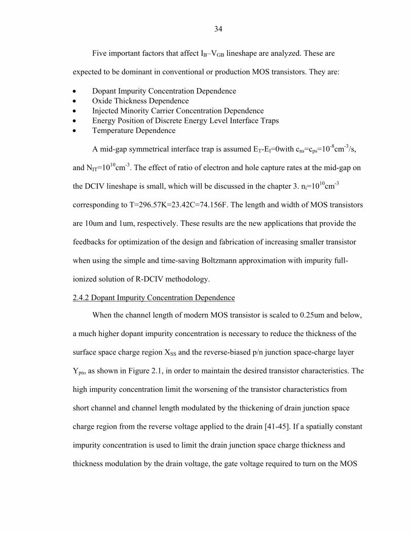
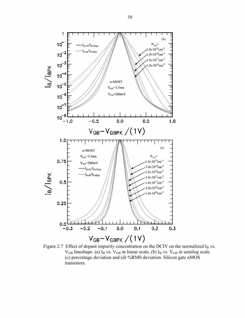
Deionization results. Figures 2.6 and 2.7 show a family of normalized theoretical
recombination DCIV curves using BI approximation solution in dash line and the FD
exact theory in solid line for metal gate case and silicon gate transistors, respectively.
For short channel and small area transistors, the DCIV current is in the Femto
ampere range. So only the current near the peak can be measured because of noise. Thus,
the lineshape and error on percentage deviation are presented in the linear scale as shown
in Figure 2.6(a) and 2.7(a). For large area and long channel transistors, the recombination
DCIV current can be in the nano-ampere range and the noise is three or more decades

36
smaller. The lineshape and errors on percentage deviation are presented in semilog scale
as shown in Figure 2.6 (b) and (c), and Figure 2.7(b) and (c), respectively.
In both Figure 2.6(a) and 2.7(a), the 10% peak current, which means 100% IB-peak down to
10% IB-peak, is covered by a gate voltage range from -0.2V to +0.2V. We can see that the
error or % deviation of the Boltzmann ionization approximation less than 8% for 1019
impurity concentration for both metal gate and silicon gate cases as shown in Figure
2.6(c) and 2.7 (c). When impurity concentration is 5×10¹⁷, which is in practical range, %
deviation is less than 1% for metal gate case, while it is less than 2% for silicon gate
devices.
Figure 2.6(d) and 2.7(d) give the %RMS deviation when matching 10% to 90% of
the theoretical curve to the experimental data. We can see that the Boltzmann
approximation gives less than 4% RMS deviation at 1019 impurity concentration for both
metal gate and silicon gate cases. For 1018 impurity concentration, the %RMS deviation
is less than 1% for metal gate case and 2% for silicon gate case, when matching 90% of
the theoretical curve to the experimental data.
As already proved by Yih Wang and Sah [40], the distortion of IB vs. VGB lineshape
is from the spatial variation of dopant impurity concentration which can be further
distorted by the spatial variation of interface trap concentration NIT, but not by NIT alone
at the interface of SiO2/Si with a constant impurity concentration. This allows us to
extrapolate the percentage deviation and %RMS for non-constant dopant impurity
concentration at the interface of a MOS transistor. For U-shaped impurity concentration
along channel with PAA =1017cm-3 in the middle of the channel PAA =1018cm-3 at the end
of the channel, the percentage deviation and %RMS error are all no more than 1% for

37
Figure 2.6 Effect of dopant impurity concentration on the DCIV on the normalized IB vs.
VGB lineshape. (a) IB vs. VGB in linear scale, (b) IB vs. VGB in semilog scale. The substrate impurity. (c) percentage deviation and (d) %RMS deviation. RMS90, RMS75(FWQM), RMS50(FWHM), RMS25 and RMS10 represent the lineshape for peak current IB-peak down to 90%, 75%, 50%, 25% and 10% of IB-peak, respectively. Metal gate nMOS transistors.
(b)
(a

38
Figure 2.6 Continued
(c)
(d)
39
Figure 2.7 Effect of dopant impurity concentration on the DCIV on the normalized IB vs.
VGB lineshape. (a) IB vs. VGB in linear scale, (b) IB vs. VGB in semilog scale. (c) percentage deviation and (d) %RMS deviation. Silicon gate nMOS transistors.
(a)
(b)
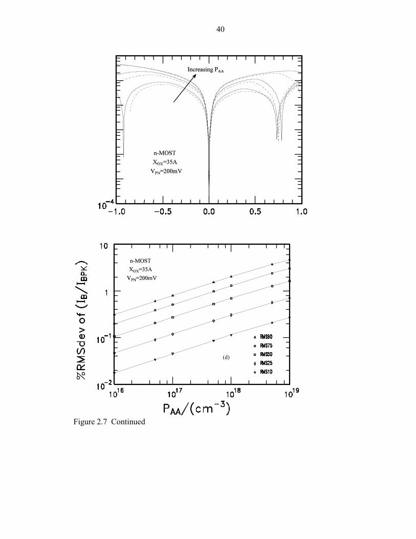
40
Figure 2.7 Continued
(d)
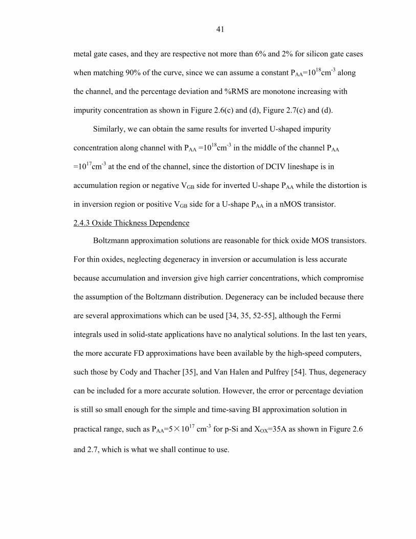
41
metal gate cases, and they are respective not more than 6% and 2% for silicon gate cases
when matching 90% of the curve, since we can assume a constant PAA=1018cm-3 along
the channel, and the percentage deviation and %RMS are monotone increasing with
impurity concentration as shown in Figure 2.6(c) and (d), Figure 2.7(c) and (d).
Similarly, we can obtain the same results for inverted U-shaped impurity
concentration along channel with PAA =1018cm-3 in the middle of the channel PAA
=1017cm-3 at the end of the channel, since the distortion of DCIV lineshape is in
accumulation region or negative VGB side for inverted U-shape PAA while the distortion is
in inversion region or positive VGB side for a U-shape PAA in a nMOS transistor.
2.4.3 Oxide Thickness Dependence
Boltzmann approximation solutions are reasonable for thick oxide MOS transistors.
For thin oxides, neglecting degeneracy in inversion or accumulation is less accurate
because accumulation and inversion give high carrier concentrations, which compromise
the assumption of the Boltzmann distribution. Degeneracy can be included because there
are several approximations which can be used [34, 35, 52-55], although the Fermi
integrals used in solid-state applications have no analytical solutions. In the last ten years,
the more accurate FD approximations have been available by the high-speed computers,
such those by Cody and Thacher [35], and Van Halen and Pulfrey [54]. Thus, degeneracy
can be included for a more accurate solution. However, the error or percentage deviation
is still so small enough for the simple and time-saving BI approximation solution in
practical range, such as PAA=5×1017 cm-3 for p-Si and XOX=35A as shown in Figure 2.6
and 2.7, which is what we shall continue to use.

42
Figures 2.8 and 2.9 respectively give one family of normalized IB vs. VGB to show the
lineshape dependence on the one of the most basic MOS transistor design parameters, the
oxide thickness (another is dopant impurity concentration), in the transistor spatial
regions where the gate voltage is designed to control the electrical characteristics of the
transistor, for metal gate and silicon gate case. Oxide thickness varies from 10A to 300A,
which covers all practical range. The lineshape broadens, and the linewidth (∆VGB+
and∆VGB-) increases as the oxide thickness and dopant impurity concentration increases
as shown in Figure 2.6 and 2.7, and Figure 2.8 and 2.9, respectively. The peak gate
voltage (VGB-peak) shifts toward the more positive gate voltage, i.e. towards increasing
hole-accumulation range in the SiO2/Si interface for a p type doped substrate.
These dependencies are anticipated by (2.15) and (2.16). They are also expected by
simple device and material physics. For instance, a higher gate voltage or electric field is
required to change the amount of surface potential or surface energy band bending in
order to reach the peak recombination rate condition, cnsNS=cpsPS, as indicated by (2.6). It
is evident that these curves are equally applicable to the p-Base of nMOS transistor and
the p-DER and p-SER of pMOS transistors.
The linear DCIV curves in Figure 2.8(a) and Figure 2.9(a) are application to short
channel application and semi-log curves in Figure 2.8 (b) and Figure 2.9(b) are for
application to long channel application of MOS transistors. The oxide thickness varies
from 13 angstroms from 300 angstroms.
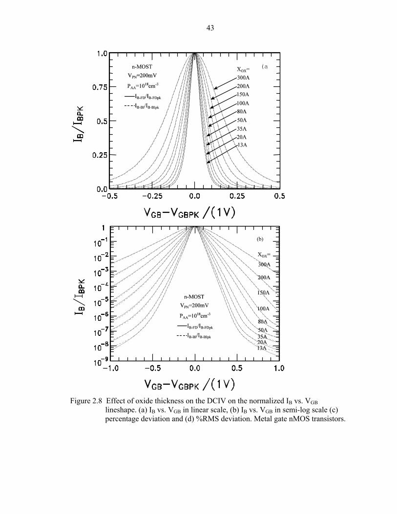
43
Figure 2.8 Effect of oxide thickness on the DCIV on the normalized IB vs. VGB
lineshape. (a) IB vs. VGB in linear scale, (b) IB vs. VGB in semi-log scale (c) percentage deviation and (d) %RMS deviation. Metal gate nMOS transistors.
(a)
(b)
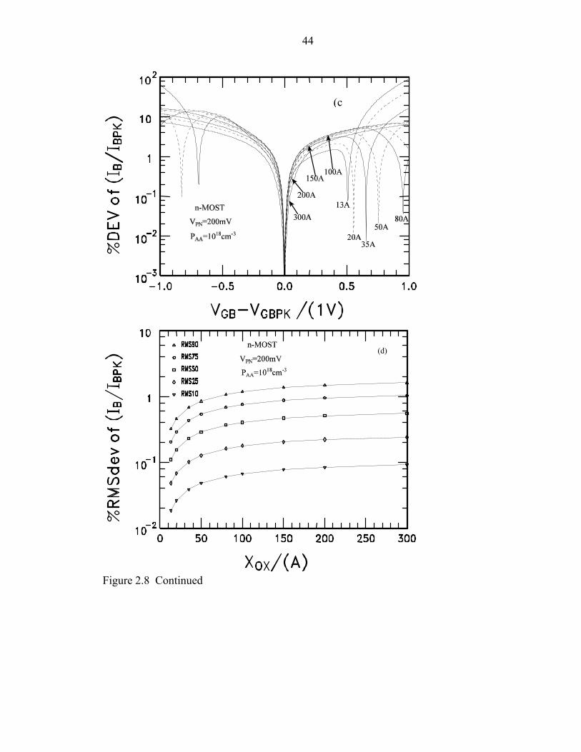
44
Figure 2.8 Continued
(d)
(c
45
Figure 2.9 Effect of oxide thickness on the DCIV on the normalized IB vs. VGB
lineshape. (a) IB vs. VGB in linear scale, (b) IB vs. VGB in semilog scale. (c) percentage deviation and (d) %RMS deviation. Silicon gate nMOS transistors.
(b)
(a)
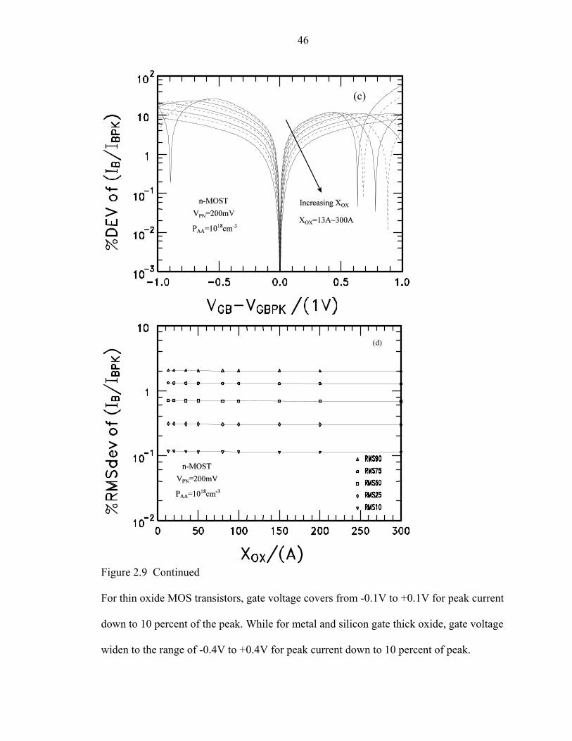
46
Figure 2.9 Continued For thin oxide MOS transistors, gate voltage covers from -0.1V to +0.1V for peak current
down to 10 percent of the peak. While for metal and silicon gate thick oxide, gate voltage
widen to the range of -0.4V to +0.4V for peak current down to 10 percent of peak.
(d)
(c)
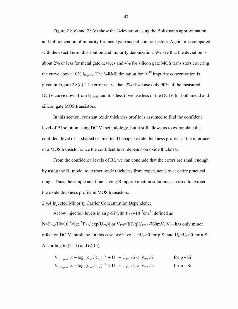
47
Figure 2.8(c) and 2.9(c) show the %deviation using the Boltzmann approximation
and full ionization of impurity for metal gate and silicon transistors. Again, it is compared
with the exact Fermi distribution and impurity deionization. We see that the deviation is
about 2% or less for metal gate devices and 4% for silicon gate MOS transistors covering
the curve above 10% IB-peak. The %RMS deviation for 1018 impurity concentration is
given in Figure 2.8(d). The error is less than 2% if we use only 90% of the measured
DCIV curve down from IB-peak and it is less if we use less of the DCIV for both metal and
silicon gate MOS transistors.
In this section, constant oxide thickness profile is assumed to find the confident
level of BI solution using DCIV methodology, but it still allows us to extrapolate the
confident level of U-shaped or inverted U-shaped oxide thickness profiles at the interface
of a MOS transistor since the confident level depends on oxide thickness.
From the confidence levels of BI, we can conclude that the errors are small enough
by using the BI model to extract oxide thickness from experiments over entire practical
range. Thus, the simple and time-saving BI approximation solutions can used to extract
the oxide thickness profile in MOS transistors.
2.4.4 Injected Minority Carrier Concentration Dependence
At low injection levels in an p-Si with PAA=1017cm-3, defined as
N<PAA/10=1016=[(ni2/PAA)exp(UPN)] or VPN=(kT/q)UPN<-760mV, VPN has only minor
effect on DCIV lineshape. In this case, we have UP=UF>0 for p-Si and UN=UF<0 for n-Si.
According to (2.11) and (2.15),
Sinfor2/V2/UU)c/c(logV
Sipfor2/V2/UU)c/c(logV
PNPNF2/1
psnsepeakGB
PNPNF2/1
psnsepeakGB
−∝++−∝
−∝−+−∝
−
−

48
Thus, gate voltage at the peak current VGB-peak would increase with forward bias VPN in
the n-Base of pMOST and decrease with VPN in the p-Base of nMOST. Low injection
level is the common application range of the DCIV methodology.
At high injection levels with VPN>~800mV, the linewidth has the exp(UPN/4)
dependence on forward bias VPN [20]. Thus, at low injection levels, the IB-VGB linewidth
can be large which is determined by the effective trap energy level, ETI*. The linewidth
then decreases with increasing VPN until the onset of high injection level condition,
beyond which it increases exponentially with VPN.
The broadening of DCIV lineshape from high injection levels could occur at lower
VPN in real transistors due to voltage-drop or VPN drop from high current density through
the lateral base resistance and series drain and source resistances, and due to gate voltage
lowering of the forward biased drain and source p/n junction barrier heights, and reduced
majority carrier concentration at surface channel from surface band bending in the sub-
threshold region. Another important source of lineshape modification comes from the
diffusion and drift current limitation on the emitter junction injection efficiency due to
built-in electric field from graded vertical (x-direction) impurity concentration profile
PAA(x,y), which is from the designed ion implantation in the bottom-emitter configuration
as shown in Figure 2.2(d). Since the diffusion-drift current is in series with the
recombination current at the interface traps, the smaller one would dominate. The
importance of the diffusion-drift limitation of the injection current has been demonstrated
using experimental data [26].
The applications of short channel and long channel of MOS transistors are given in
the linear Figure 2.10(a) and Figure 2.11(a), in the semi-log curves in Figure 2.10(b) and
49
2.11(b). The figures for metal gate and silicon gate MOS transistors are respectively
shown in Figure 2.10 and 2.11. The injected minority carrier concentration is increased
from forward bias of 100mV from 800mV. For small injection minority carrier
concentration, gate voltage covers from -0.1V to +0.1V for peak current down to 10
percent of the peak. While, gate voltage should change from -0.25V to +0.25V for peak
current down to 10 percent of peak for high injection MOS transistors.
Figure 2.10(c) and 2.11(c) show the %deviation using the Boltzmann
approximation and full ionization of impurity for metal gate and silicon gate transistors.
Again, it is compared with the exact Fermi distribution and impurity deionization. We see
that the deviations are respectively about 6% and 10% for metal gate and silicon gate
devices when matching 90% of experimental data from peak current IB-peak down to 10%
of the peak using Boltzmann full ionization approximation solution.
The %RMS deviation for 1018 impurity concentration is given in Figure 2.10(d) and
2.11(d). The error is around less than 3% for forward bias VPN smaller than 600mV and
6% for VPN smaller than 800mV if we use only 90% of the measured DCIV curve for
metal gate transistors. While in silicon gate devices, these two values are respectively 4%
and 8%.The %RMS deviation is less than 0.4% if we match only 10% of DCIV curves to
experiments for both metal gate and silicon gate cases.
These values of % deviation and %RMS deviation indicate that the Boltzmann full
ionization approximation solution is good enough to extract the parameters of MOS
transistors when forward bias VPN is in practical range.
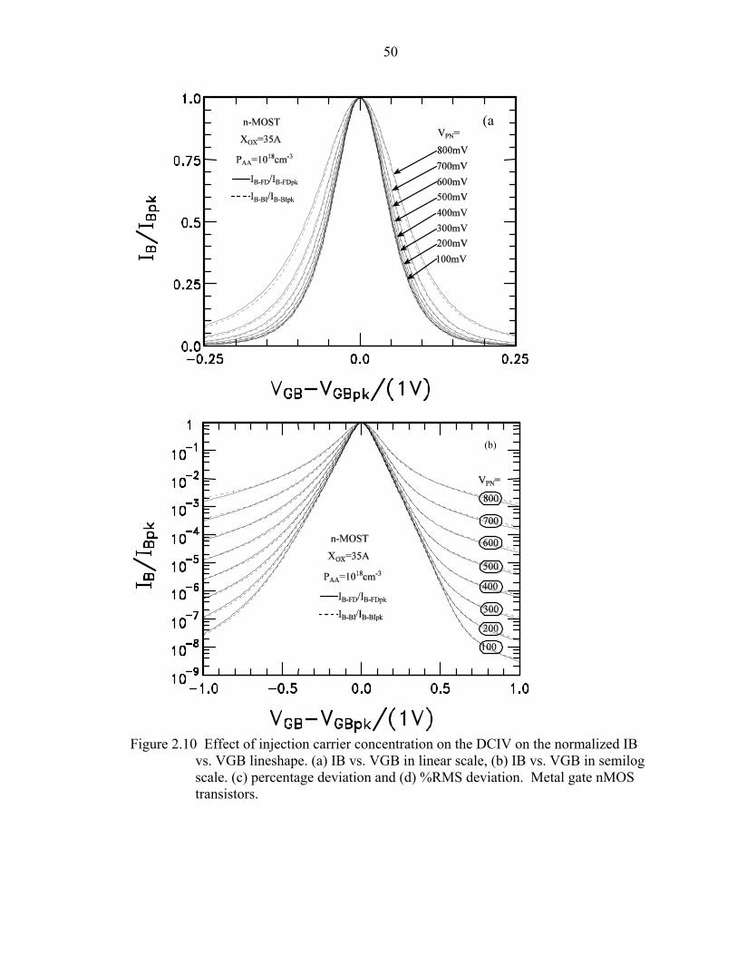
50
Figure 2.10 Effect of injection carrier concentration on the DCIV on the normalized IB
vs. VGB lineshape. (a) IB vs. VGB in linear scale, (b) IB vs. VGB in semilog scale. (c) percentage deviation and (d) %RMS deviation. Metal gate nMOS transistors.
(b)
(a
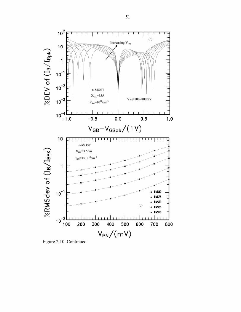
51
Figure 2.10 Continued
(d)
(c)
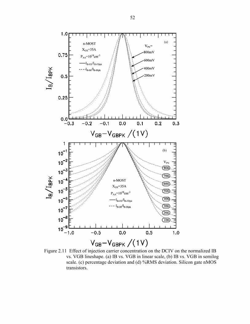
52
Figure 2.11 Effect of injection carrier concentration on the DCIV on the normalized IB
vs. VGB lineshape. (a) IB vs. VGB in linear scale, (b) IB vs. VGB in semilog scale. (c) percentage deviation and (d) %RMS deviation. Silicon gate nMOS transistors.
(b)
(a)
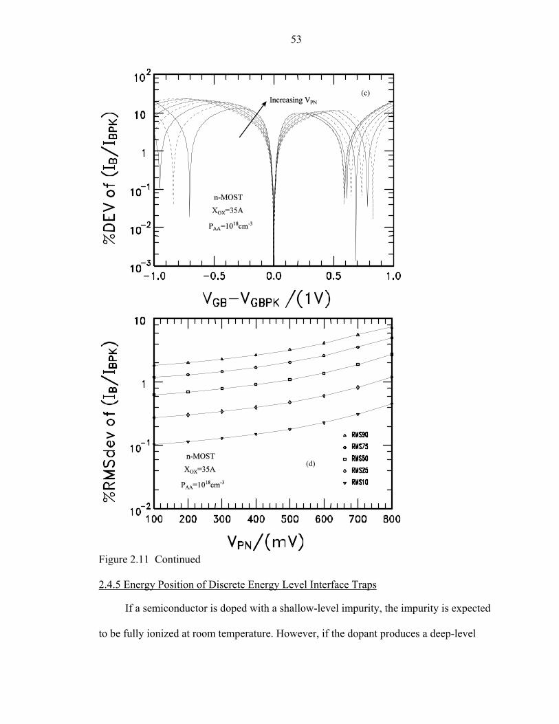
53
Figure 2.11 Continued
2.4.5 Energy Position of Discrete Energy Level Interface Traps
If a semiconductor is doped with a shallow-level impurity, the impurity is expected
to be fully ionized at room temperature. However, if the dopant produces a deep-level
(d)
(c)
54
trap, deionization will become a significant factor regardless of the doping concentration
or temperature.
According to (2.7) and (2.12), the interface trap energy level ETI determines the
DCVI linewidth. As shown in Figure 2.10 and 2.11, the lineshape changes with
increasing forward biases, VPN, applied to an n/p junction in p-Si with an acceptor
impurity concentration PAA=1018cm-3, an oxide thickness of 3.5nm, and a discrete
interface trap at mid-gap (ETI=0). Figures 2.12(a) and 2.13(a) give the effect of the
interface trap energy level position on the recombination DCIV lineshape for metal gate
and silicon gate transistors, respectively. These figures are for 1-discrete interface trap
level. The reference of interface trap level is intrinsic Fermi level or mid-gap. If forward
bias is less than interface trap energy, i.e., VPN<ETI/q, there is a flat-top region around the
peak current IB-peak and the lineshape is symmetrically broadened by shallower energy
level traps, such as 0.2eV and 0.3eV traps. Note, the broad top is the distinct signature of
a shallow interface trap energy level. The application on large area and long channel
transistors is given in Figure 2.12(b) and 2.13(b) The %deviations for Boltzmann
ionization approximation are given in Figure 2.12(c) and 2.13(c). Since gate voltage
varies from -0.5V to +0.5V for peak current down to 10 percent of the peak for shallow
trap levels, such as ETI=300mV. The %deviation is about 8% for metal gate devices and
15% for silicon gate transistors when matching 90% of experiment DCIV curve to theory
using Boltzmann ionization approximation solutions. At mid-gap level, which is the
commonest assumption for interface trap level during computations using DCIV
mythology, the %deviation are less than 2% for metal gate devices and 5% for silicon

55
gate transistors. Figure 2.12(d) and 2.13(d) show the %RMS deviation using 10% to 90%
of the theoretical
Figure 2.12 Effect of energy position of discrete interface trap energy level on the DCIV
on the normalized IB vs. VGB lineshape. (a) IB vs. VGB in linear scale, (b) IB vs. VGB in semi-log scale. (c) percentage deviation and (d) %RMS deviation. Metal gate nMOS transistors.
(b)
(a)
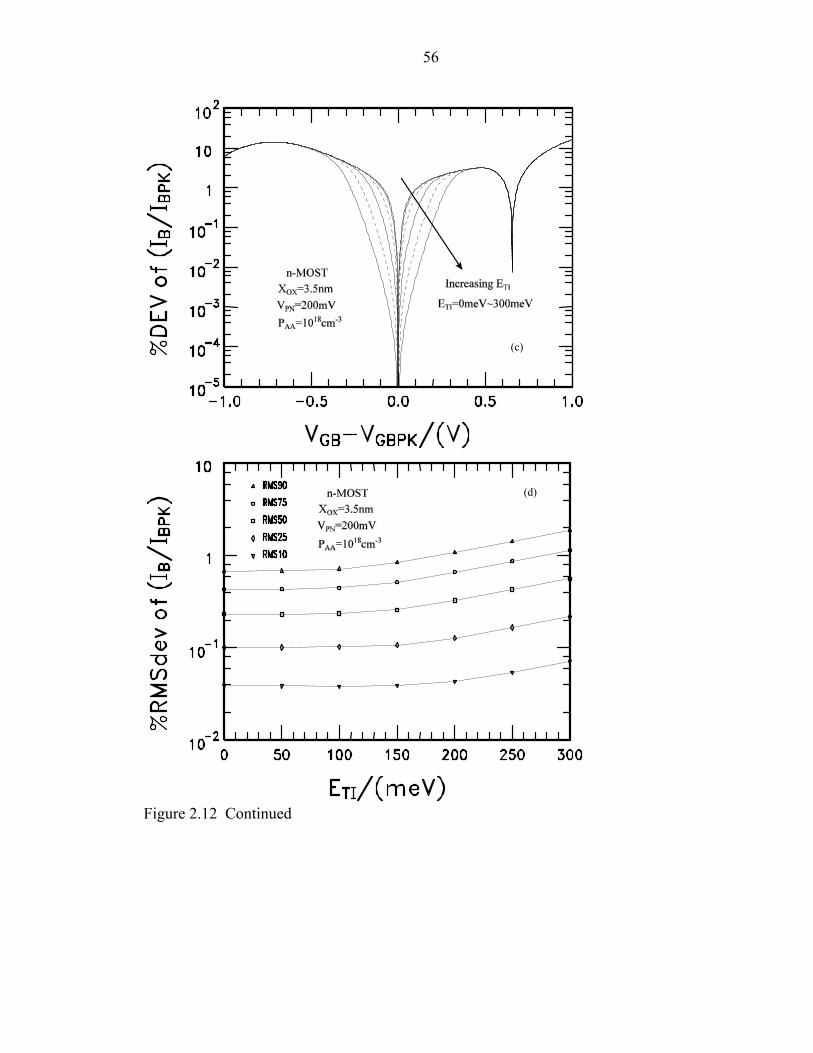
56
Figure 2.12 Continued
(d)
(c)
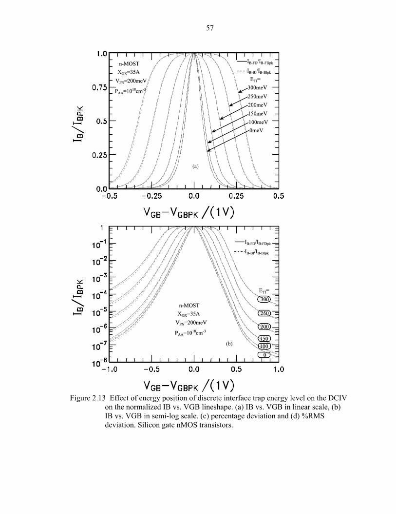
57
Figure 2.13 Effect of energy position of discrete interface trap energy level on the DCIV
on the normalized IB vs. VGB lineshape. (a) IB vs. VGB in linear scale, (b) IB vs. VGB in semi-log scale. (c) percentage deviation and (d) %RMS deviation. Silicon gate nMOS transistors.
(b)
(a)
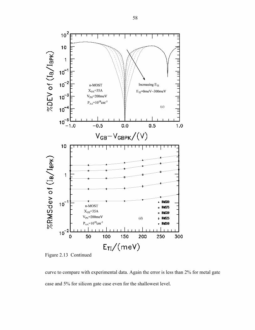
58
Figure 2.13 Continued
curve to compare with experimental data. Again the error is less than 2% for metal gate
case and 5% for silicon gate case even for the shallowest level.
(d)
(c)
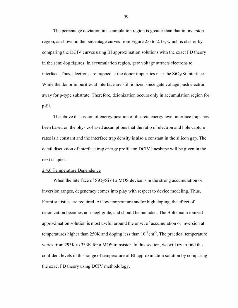
59
The percentage deviation in accumulation region is greater than that in inversion
region, as shown in the percentage curves from Figure 2.6 to 2.13, which is clearer by
comparing the DCIV curves using BI approximation solutions with the exact FD theory
in the semi-log figures. In accumulation region, gate voltage attracts electrons to
interface. Thus, electrons are trapped at the donor impurities near the SiO2/Si interface.
While the donor impurities at interface are still ionized since gate voltage push electron
away for p-type substrate. Therefore, deionization occurs only in accumulation region for
p-Si.
The above discussion of energy position of discrete energy level interface traps has
been based on the physics-based assumptions that the ratio of electron and hole capture
rates is a constant and the interface trap density is also a constant in the silicon gap. The
detail discussion of interface trap energy profile on DCIV lineshape will be given in the
next chapter.
2.4.6 Temperature Dependence
When the interface of SiO2/Si of a MOS device is in the strong accumulation or
inversion ranges, degeneracy comes into play with respect to device modeling. Thus,
Fermi statistics are required. At low temperature and/or high doping, the effect of
deionization becomes non-negligible, and should be included. The Boltzmann ionized
approximation solution is most useful around the onset of accumulation or inversion at
temperatures higher than 250K and doping less than 1018cm-3. The practical temperature
varies from 293K to 333K for a MOS transistor. In this section, we will try to find the
confident levels in this range of temperature of BI approximation solution by comparing
the exact FD theory using DCIV methodology.
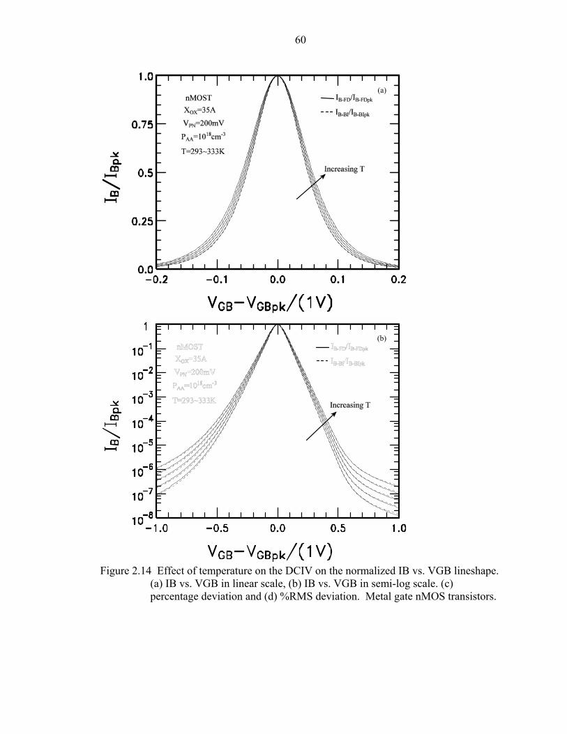
60
Figure 2.14 Effect of temperature on the DCIV on the normalized IB vs. VGB lineshape.
(a) IB vs. VGB in linear scale, (b) IB vs. VGB in semi-log scale. (c) percentage deviation and (d) %RMS deviation. Metal gate nMOS transistors.
(b)
(a)

61
Figure 2.14 Continued
(d
(c)
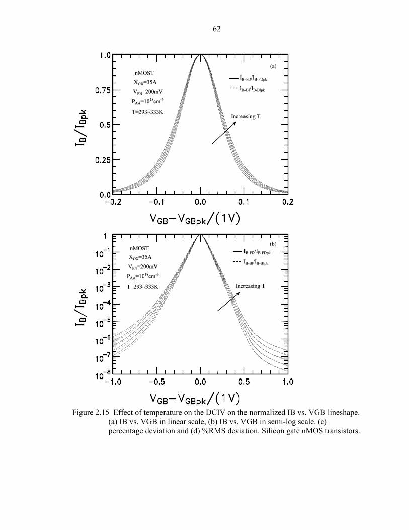
62
Figure 2.15 Effect of temperature on the DCIV on the normalized IB vs. VGB lineshape.
(a) IB vs. VGB in linear scale, (b) IB vs. VGB in semi-log scale. (c) percentage deviation and (d) %RMS deviation. Silicon gate nMOS transistors.
(b)
(a)

63
Figure 2.15 Continued
The temperature dependence of surface recombination current in the basewell
channel region is mainly determined by the temperature dependence of intrinsic carrier
concentration ni, in which, the effective density state in conduction band NC and in
(d)
(c)
64
valence band NV and silicon energy gap EG are functions of temperature. Thus, the
transistor characteristics are temperature dependent.
The linear DCIV curves in Figure 2.14(a) and 2.15(a) are for short channel
application and semilog curves in Figure 2.14(b) and 2.15(b) for the application of long
channel and large area MOS transistors. In this temperature range, gate voltage covers
from -0.15V to +0.15V for peak current IB-peak down to 10 percent of the peak for both
metal gate and silicon gate transistors.
Figure 2.14(c) and 2.15(c) show the %deviation using the Boltzmann
approximation and full ionization of impurity by comparing with the exact Fermi
distribution and impurity deionization. We see that the deviation is about 2% or less for
metal gate case and 5% for silicon gate case when marching peak current IB-peak down to
10% of the peak. The %RMS deviations are given in Figure 2.14(d) and 2.15(d). The
error is less than 1% for metal gate transistors and 2% for silicon gate devices if we use
only 90% of the measured DCIV curve and it is less if we use less of the DCIV.
These confidence levels indicate that temperature fluctuation gives negligible errors
when using BI approximation solutions to extract the parameters such as surface dopant
impurity concentration and interface trap concentration profiles and oxide thickness
profile in a MOS transistor.
A detail discussion about temperature effect on DCIV lineshape, peak current
amplitude IB-peak, peak gate voltage VGB and thermal active energy EA at different
interface trap energy levels ETI will be described in the next chapter.
65
2.5 Summary
Effects from variation at the SiO2/Si interface of the dopant impurity concentration
PAA, oxide thickness XOX, the injected minority carriers VPN, energy position of interface
trap level ETI and temperature T on the lineshape of the DCIV IB-VGB curves are
analyzed. The confident level or deviation from using the Boltzmann ionization
approximation instead of the exact Fermi Deionization theory is computed. It is
illustrated by a family curves that BI and FI solutions are respectively found to be nearly
as good as BD and FD solutions, particularly in inversion region where deionization is
less a factor. For a practical MOS transistor with VPN=200mV, XOX=35A, PAA=1018cm-3,
ETI=0.0eV and T=296.57K, the percentage deviation and %RMS deviation are
respectively no more than 2% and 1% for metal gate devices, and 4% and 2% for silicon
gate transistors when matching 90% of DCIV curves from peak current to experimental
data using Boltzmann ionized approximation solutions. These results indicate that the
simple and time-saving BI approximation solutions of R-DCIV methodology are good
enough to extract the spatial concentration profiles of the dopant impurity and interface
trap at the SiO2/Si interface and the oxide thickness profile in modern MOS transistors.
66
CHAPTER 3 R-DCIV LINESHAPES FROM DISTRIBUTED ENERGY LEVELS OF INTERFACE
TRAPS IN SILICON GAP
3.1 Introduction
In this chapter, we analyze the effect of the energy level distribution of interface
trap on the R-DCIV lineshape. First, we give a review. Interface properties along the
channel have dominated the electrical characteristics and performance, and reliability of
MOS transistors. Due to the technological importance, extensive research efforts have
been undertaken to study interfacial electronic traps at the SiO2/Si interface and to
delineate their microscopic origin [56, 57]. First, we will review the history of interface
traps or surface states at the interface of SiO2/Si in a MOS transistor.
For a Schottly diode, the current formula is I(M/S)=I0*exp(qV/kT), where
I0=A*exp(-ΦB/kT) is dark current or saturation current. The reverse current is dependent
on the work function difference between metal and semiconductor. It should be different
values when using different metals. However, Mayerhof [58] in 1946 observed metal-
independent Schottly barrier height. In1947, John Bardeen [59] presented two models of
interface trap level distribution to account for Mayerhof’s results. One proposed
distribution of density of interface state was U-Shaped that rises towards the two band
edges. This is from random variations of Si-O bond length and bond angles as explained
by Sah [56, 57]. The second was the two-level interface traps [59]. Two-level interface
traps are from periodic dangling silicon bond [57].

67
In 1948, Shockley-Pearson [60] used thin film FET (Field Effect Transistor) to find
a solid-state replacement of a vacuum tube. But they found no conductivity modulation in
the FET. The null result was attributed to high density of interface states. High density of
interface traps will pin or lock the position of the Fermi level at the surface of the thin
Silicon film [56, 57, 59, 61] since band bending from the metal/semiconductor work
function difference is negligible compared with that due to the high density of interface
traps. So the voltage applied to the metal gate over air-gap will not modulate the
conductance or resistance of the thin silicon film on glass. The pinning or locking of the
Fermi level to the neutral Fermi level position at the metal/semiconductor interface not
only causes the experimental Schottky barrier height to differ from that calculated using
the vacuum work function value of the metal but also makes the Si surface band bending
or barrier height nearly independent of the type of metal or conductor used for the
metal/Si Schottky diodes [61].
There was another experimental uncertainty of experimental level determined by
the thermal activation (or temperature dependence) of a device current. In 1957, Sah-
Noyce-Shockey [31] used theory to fit experimental data in order to obtain the bulk trap
energy level. What they found was that the trap energy levels were always near the mid-
gap over a small energy range for many different p/n junctions. These values are not
unique since different matching points will give different energy level. In addition, what
was measured was (2.9), ETI*=ETI+kTln(cns/cps), not ETI.
Another historical example was reported on the uncertainty of the interface trap
energy levels in1962. Sah [8] observed two discrete energy levels using recombination R-
DCIV methodology. However, the two levels may come from the same interface trap
68
energy level because in a very thick oxide transistor, a non-uniform impurity
concentration would shift peaked base current versus gate voltage from one into two
locations.
In 1971, Nishi [62] obtained discrete interface trap energy levels on large area and
thick oxide using EPR (Electron Paramagnetic or Spin Resonance). The area is around
one square centimeter and the oxide thickness is around one micrometer. For modern
transistors, the area is much smaller than one square centimeter (~1um2) and oxide
thickness is much less than one micrometer (~10-3 micrometer or 1nm). Therefore, the
discrete energy level obtained from EPR is not likely the interface trap in modern MOS
transistors. One limitation using EPR is its lack of sensitivity, needing 1013-1014 spins
per square centimeter to detect the signal. For modern MOS transistors with 1018cm-3
impurity concentrations, 250nm of channel length and width, there are only 60 traps at
1011cm-2 or 6000 traps at 1013cm-2. Therefore, it is impossible to observe the EPR
signal even on the state-of-the-art transistors.
The R-DCIV methodology has been proposed to extract device properties of deep
submicron MOS transistor with spatial nanometer resolutions (or 10 atomic layers) which
can not be obtained by conventional metallurgical-optical techniques. In this novel
method, the d.c. current voltage characteristics are measured and then analyzed by
device-physics-based analytical theory to give the device and material properties. The
novelty is the selection of the particular electrical characteristics which are very sensitive
to the material properties in these devices, but also insensitive to multi-dimensional
effects.

69
The d.c. recombination current at basewell terminal, IB, is modulated by the applied
gate/base voltage, VGB, in a MOS transistor. This method was used to monitor electric-
field-stress generated interface traps as a transistor reliability monitor [11, 15, 26, 57] and
to serve as pre-stress diagnostic monitor for transistor design and processing [26]. The IB
modulated by gate voltage VGB arises from recombination of the majority carrier at the
SiO2/Si interface traps under the gate oxide with the injected minority carriers by one or
more forward biased p/n junctions (Drain/Base, Source/Base, and Substrate/Basewell)
into the basewell. The R-DCIV peak current IB-peak and its lineshape are highly sensitivity
to the transistor design, such as channel L and width W, the spatially variation of the
dopant impurity and interface trap concentrations along the SiO2/Si interface, and the
profile of interface trap energy level over the silicon gap in MOS transistors. A detailed
theoretical analysis on R-DCIV methodology was presented in the chapter 2 for basewell
channel region (BCR). The recombination at the interface traps in space charge region of
source junction (SJR) and drain extension region (DER) becomes increasingly important
in unstressed transistors as the channel length is scaled down and it is well-known that
recombination in SJR dominates in stressed transistors [15,10,21] regardless of the
channel length [15,18].
In this chapter, Slater’s perturbation theory [63] is used to explain the two models
of interface trap energy distributions described by Sah [57] as shown in Figure 3.1. The
energy band diagram in Fig 3.1(a) is for ideal case, zero traps at interface and in the bulk.
The band diagrams in Fig 3.1(b) and Fig 3.1(c) are for bulk traps from perturbation in the
silicon bulk. All the localized energy level with symmetry wave function will be pushed
up when the localized perturbation from the trap potential ∆ is positive (such as P type
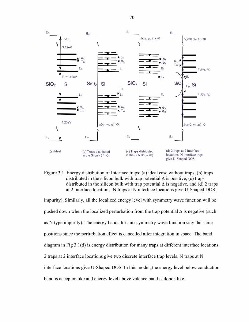
70
Figure 3.1 Energy distribution of Interface traps: (a) ideal case without traps, (b) traps
distributed in the silicon bulk with trap potential ∆ is positive, (c) traps distributed in the silicon bulk with trap potential ∆ is negative, and (d) 2 traps at 2 interface locations. N traps at N interface locations give U-Shaped DOS.
impurity). Similarly, all the localized energy level with symmetry wave function will be
pushed down when the localized perturbation from the trap potential ∆ is negative (such
as N type impurity). The energy bands for anti-symmetry wave function stay the same
positions since the perturbation effect is cancelled after integration in space. The band
diagram in Fig 3.1(d) is energy distribution for many traps at different interface locations.
2 traps at 2 interface locations give two discrete interface trap levels. N traps at N
interface locations give U-Shaped DOS. In this model, the energy level below conduction
band is acceptor-like and energy level above valence band is donor-like.
SiO2
EV
3.12eV
4.25eV
EV EV(y2, z2)
SiO2
EC
EC
EC
EV EV
EC
∆=0
ΦSΦA
ΦAΦS
EV
SiO2
EC
EC
∆(x1, y1, z1) <0
EC(y1, z1)
(a) Ideal (b) Traps distributed in the Si bulk (Δ>0)
(d) 2 traps at 2 interface locations. N interface traps give U-Shaped DOS
(c) Traps distributed in the Si bulk (Δ<0)
∆(x=0, y2, z2) >0
∆(x=0, y1, z1) <0
EG=1.12eV
ΦSΦA
ΦAΦS
ΦAΦS
EV
Si Si Si Si
ΦAΦS
∆(x2, y2, z2) >0
ED
EA EA
ED
EC
EV
ΦA ΦS
SiO2
71
The lineshape of R-DCIV is primarily determined by the dopant impurity
concentration and its areal profile at the SiO2/Si interface, and only secondarily
determined by the areal variation of the interface trap concentration provided the impurity
concentration is not a constant. The injected minority concentration at the interface gives
only a small change of the lineshape for the usually encountered dopant impurity
concentration profiles. However, energy distribution of interface traps is assumed at the
mid-gap (ETI=0) in these cases. There is negligible lineshape change between the three
distributions of density of interface traps: a discrete level at the mid-gap, a constant
density of traps over the entire silicon gap, and a U-shape density of traps if we assume
that the electron capture rates is equal to hole capture rate in silicon energy gap.
A U-shaped density of traps in silicon gap with a U-shaped ratio of electron and
hole-capture rates for a constant impurity concentration profile over the channel can still
broaden the lineshape, which will be shown in this chapter. Thus, lineshape, peak current
IB-peak and peak gate voltage VGB-peak of R-DCIV curves may give the energy distribution
of interface traps. Families of base current versus gate/base voltage (IB-VGB) are
computed to illustrate the effects of energy level of interface traps which could extract a
possible energy distribution in the silicon gap from experimental R-DCIV lineshape. The
potential applications from the analysis are proposed.
3.2 Effect of ratio of electron and hole capture rates at mid-gap trap
The analytical formula were derived and described in chapter 2 for the Shockley-
Read-Hall (SRH) steady-state recombination rate RSS at interface traps in the basewell
channel region (BCR). We first examine the effect of the cns and cps on the R-DCIV
lineshape. In (2.7), the electron capture rate is assumed to equal to hole capture rate, i.e.,
cns=cps=10-8cm3/s, generally the capture cross section, effective mass and thermal-
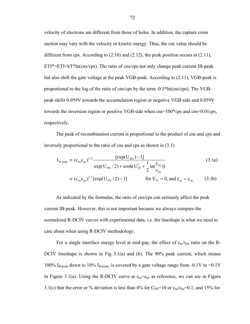
72
velocity of electrons are different from those of holes. In addition, the capture cross
section may vary with the velocity or kinetic energy. Thus, the cns value should be
different from cps. According to (2.10) and (2.12), the peak position occurs at (2.11),
ETI*=ETI+kT*ln(cns/cps). The ratio of cns/cps not only change peak current IB-peak
but also shift the gate voltage at the peak VGB-peak. According to (2.11), VGB-peak is
proportional to the log of the ratio of cns/cps by the term -0.5*ln(cns/cps). The VGB-
peak shifts 0.059V towards the accumulation region or negative VGB side and 0.059V
towards the inversion region or positive VGB side when cns=100*cps and cns=0.01cps,
respectively.
The peak of recombination current is proportional to the product of cns and cps and
inversely proportional to the ratio of cns and cps as shown in (3.1)
)b3.1(ccand,0Efor]1)2/U[exp()cc(
)a1.3())
ccln(
21Ucosh()2/Uexp(
]1)U[exp()cc(I
psnsTIPN2/1
psns
ps
ns*TIPN
PN2/1psnspeakB
==−∝
++
−∝−
As indicated by the formulas, the ratio of cns/cps can seriously affect the peak
current IB-peak. However, this is not important because we always compare the
normalized R-DCIV curves with experimental data, i.e. the lineshape is what we need to
care about when using R-DCIV methodology.
For a single interface energy level at mid-gap, the effect of cns/cps ratio on the R-
DCIV lineshape is shown in Fig 3.1(a) and (b). The 90% peak current, which means
100% IB-peak down to 10% IB-peak, is covered by a gate voltage range from -0.1V to +0.1V
in Figure 3.1(a). Using the R-DCIV curve at cns=cps as reference, we can see in Figure
3.1(c) that the error or % deviation is less than 4% for CPN=10 or cns/cps=0.1, and 15% for
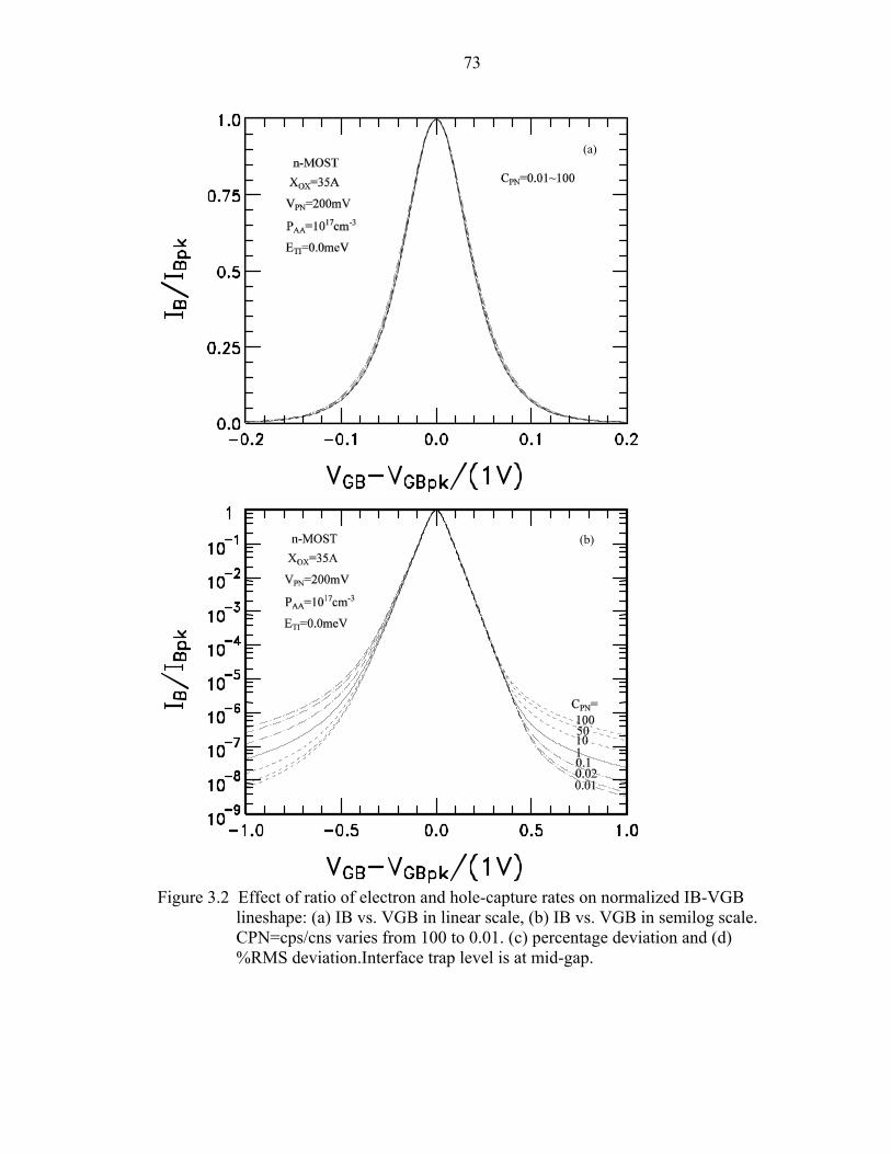
73
Figure 3.2 Effect of ratio of electron and hole-capture rates on normalized IB-VGB
lineshape: (a) IB vs. VGB in linear scale, (b) IB vs. VGB in semilog scale. CPN=cps/cns varies from 100 to 0.01. (c) percentage deviation and (d) %RMS deviation.Interface trap level is at mid-gap.
(b)
(a)

74
Figure 3.2 Continued CPN=0.01 or cns/cps=100. The %RMS deviation is around 8% for cns/cps =100 as shown in
Figure 3.1(d). While the percentage deviation and %RMS error are respectively smaller
than 10% and 6% for CPN=0.1 or cns/cps =10. In practice, since the effective electron mass
(d)
(c)

75
is smaller than the effective mass of hole, the cns value may be greater than cps. Thus, the
ratio of cns/cps only gives a small change of lineshape for a single interface level at mid-
gap.
The ratio of cns/cps at the mid-gap energy level could vary in a range from 0.01 to
100. According to this family figure, the ratio of cns/cps at the mid-gap has only a minor
effect on R-DCIV lineshape for a single interface energy level right at the mid-gap.
3.3 Effect of Distribution of Interface Trap Energy Level on R-DCIV Lineshape
In the preceding sections, we have already tested the effect of cns/cps ratio on R-
DCIV lineshape for single interface energy level at mid-gap. There are several possible
combinations of energy dependence between density of interface traps and the ratio of
cns/cps over the silicon gap: (1) a constant density of interface traps with a constant
cns/cps, (2) a constant density of interface traps with a U-shaped cns/cps, (3) a U-shaped
density of interface traps with a constant cns/cps, (4) a U-shaped density of interface
traps with a U-shaped cns/cps. Since capture rate is a function of energy position in
silicon gap, cns could be several orders greater than cps when interface energy level is
close to conduction band. Similarly, cps could be several orders greater than cns when
interface energy level is close to valence band. According to Slater’s perturbation theory,
interface trap levels are those localized energy levels with symmetry wave function in
conduction and valence bands, shifted into silicon gap by localized perturbation potential.
Thus, the density of interface traps near the conduction and valence bands should be
greater than those at around mid-gap. Therefore, the combinations of energy level
distribution of interface trap in (1), (2) and (3) may not be possible. The most probable
combination is the last one, i.e., a U-shaped density of interface traps and a U-shaped
ratio of cns/cps over the silicon gap. In this section, we then investigate the distribution of
76
interface trap level ETI with a U-shaped cns/cps ratio in silicon gap on the R-DCIV or
IB-VGB lineshape. Since the cns/cps ratio is a function of interface trap level, we will not
study the case for a constant cns/cps ratio over the silicon gap.
Before we look into the effect of energy position of interface traps, we should first
give the definition of U-shaped distribution in silicon gap. For density of interface traps, a
U-shape distribution has a minimum interface state density (NIT=1010cm-2) at mid-gap
(or ETI=0) and rises towards the two band edges (conduction and valence bands).
Similarly, a U-shaped distribution for the ratio of electron and hole capture rates cns/cps
has cns=cps=10-8cm3/s at mid-gap and rises towards the two band edges, and cns is
several orders greater than cps at the edge of conduction band and cps is several orders
greater than cns. Both density of interface trap states and cns/cps ratio are functions of
energy position of interface traps, i.e., NIT=ƒ(ETI) and cns/cps =ƒ(ETI) . For simplicity,
we will not include the temperature effect on the two distributions in silicon gap and a
normalized energy level of interface traps ETIN is introduced for this purpose. The
formulae of density of interface traps, electron and hole capture rates are given
)E
Eexp(10c),EE(exp10c
)EEcosh(10N
TIN
TI8ps
TIN
TI8ns
TIN
TI10IT
−×=×=
×=
−−
In our computations, the value of ETIN equals to 0.0625eV so that density of
interface states at the two band edge is around NIT≈5.0*1013cm-2 and the electron and
hole capture rates are respectively 2.5*106 or around seven orders greater than hole and
electron capture rates respectively at the edge of conduction and valence bands.
In an R-DCIV measurement, the contribution of each of interface trap energy level
can be added to give the total contribution to recombination current IB. Computed
77
examples are given to show the effects on the R-DCIV lineshape using the following
formula.
)2.3(dydE)Ucosh()Ucosh()2/Uexp(
)E(N]1)U[exp(2
Wn)cc(qI TI*
TI*sPN
TIITPNi21
psnsB ∫∫ +
−=
The interface traps are each characterized by its electron and hole capture rate
coefficients, cns and cps, and its energy level in the silicon energy gap, ETI, which is
measured from the intrinsic Fermi position near the silicon mid-gap. These three
properties define the star interface trap energy level,
ETI*=ETI+kTln(cns/cps)1/2=UTI*(kT/q), at which the steady-state recombination rate peaks
and begins to decrease due to the increase of the electron or hole surface concentration by
the applied gate voltage, VGB.
Since we don’t know if the interface trap level in silicon gap is only 1 level at the
mid-gap, it is necessary to investigate the effect of cns/cps ratio on the lineshape for
multi-interface trap levels. The effect of cns/cps ratio on the R-DCIV lineshape is shown
in Fig 3.2(a) and (b) for a U-shaped density of interface traps and a U-shaped cns/cps
ratio over the silicon gap. The ratio of CPN labeled in the figures 3.2(a) and (b) is for the
mid-gap level. For instance, the formulas of cns and cps are changed into cns=10-
10*exp(ETI/ETIN) and cps=10-8*exp(ETI/ETIN) for CPN=cps/cns=100, the CPN ratio
at other trap levels are computed using these two formulas. The 10% peak current is
covered by a gate voltage range from -0.15V to +0.15V in Figure 3.2(a). Again, using the
R-DCIV curve from the mid-gap level with cns=cps as reference, we can see in Figure
3.2(c) that percentage deviation is less than 30% for CPN=0.01 or cns/cps =100. The
%RMS deviation is around 8% for cns/cps =100 as shown in Figure 3.2(d). The

78
percentage deviation and %RMS error are respectively smaller than 10% and 4% for
CPN=0.1 or cns/cps =10. Thus, the cns/cps ratio only gives a small change of lineshape
for a U-shaped density of interface trap and a U-shaped cns/cps over the silicon energy
gap.
According to figures 3.1 and 3.2, the ratio of cns/cps has only a minor effect on R-
DCIV lineshape for both a single interface energy level right at the mid-gap and a U-
shaped distribution of density of interface trap with a U-shaped cns/cps over the silicon
gap. Thus, for the analysis convenience, we can assume the ratio of cns/cps equals to 1 or
cns=cps at the mid-gap in the followings for the discussion of energy distribution of
interface traps.
For interface trap level at the edge of conduction band, electron capture and
emission rates are respectively much greater than hole capture and emission rates. From
(2.6), we have
)b3.3(CBofedgetheat,NnN
)Uexp(nc
)a3.3(N)pP(c)nN(c
)nPN(cc
)6.2(NePceNc
eePNccR
IT1s
PN2ips
IT1sps1sns
2isspsns
ITpsspsnssns
psnssspsnsSS
+≈
+++−
=
+++−
=
)d3.3(VBofedgetheat,)Uexp(NeR)c3.3(CBofedgetheat,)Uexp(NeR
PNITnspeakSS
PNITpspeakSS
≈
≈
−
−

79
Figure 3.3 Effect of ratio of electron and hole-capture rates on normalized IB-VGB
lineshape: (a) IB vs. VGB in linear scale, (b) IB vs. VGB in semilog scale.. (c) percentage deviation and (d) %RMS deviation. Density of interface traps is U-shaped and the ratio of cps/cns = CPN.
(b)
(a)
80
Figure 3.3 Continued
In (3.3a) and (3.3b), n1 and p1 are respectively electron and hole concentrations
when Fermi level EF coincides interface trap level ET. At the edge of conduction band,
the product of surface electron and hole concentration is much greater than intrinsic
(d)
(c)
81
carrier concentration, i.e., NSPS=ni2exp(UPN)>>ni2, and cns>>cps, ens>>eps, and
n1>>p1. Thus, we can ignore the term ni2 in numerator and cps(PS+p1) in denominator
of in (3.3a), and equation (3.3a) can be simplified into (3.3b). Since n1 is much greater
than NS, NS can dropped in (3.3b) near the peak recombination current, IB-peak. Using
eps=cpsn1, we have a formula of steady-state recombination rate near the peak at the
edge of conduction band as shown in (3.3c). From this formula, it is obviously that the
emission rate of holes dominates RSS recombination rate because it is the lowest among
the four transitions as shown in Figure 2.4. Similarly, a formula RSS recombination rate
near the peak at the edge of valence band can be obtained in (3.3d) using the same
procedures. In this case, the emission rate of electrons dominates RSS since it is the
lowest among the four transitions.
According to (3.3c) and (3.3d), for a constant forward bias VPN, the contribution
from a interface trap level above or below mid-gap may give a recombination current
with sharp peak, which is dependent on the product of electron or hole emission rate (eps
or ens) and density of interface states NIT at the level. Normally, the contribution from
an interface level at the edge of conduction or valence bands give a R-DCIV curve with a
maximum flat-top since the hole or electron emission rate is around seven orders smaller
than that at the mid-gap, while the density of interface states is only three orders greater
than that at the mid-gap. Thus, interface trap levels that can contribute a sharp peak R-
DCIV curve are those trap levels at around the silicon mid-gap. This result confirms that
the most effective recombination centers are those interface traps with energy close to the
mid-gap [31].
82
Figure 3.4 Effect of discrete and asymmetrical interface trap energy distribution on IB-
VGB lineshape: (a) Two interface trap energy levels ETI =0, 0.2eV. (b) Three interface trap energy levels ETI=0, 0.1, 0.2eV. (c) Eleven ETI varies from 0 to 0.5eV with a step of ETI =0.05eV. (d) Eleven ETI varies from 0 to -0.5eV with a step of ETI =-0.05eV. NIT=ƒ(ETI) and cns/cps=ƒ(ETI).
(b)
(a)
83
Figure 3.4 Continued
Figures 3.3 (a) to (d) show the effect of many energy levels on the IB-VGB
lineshape. According to equations in (2.11) and (2.15), gate voltage at the peak current
VGB-peak is proportional to the log of electron and hole capture rate ratio, cns/cps, i.e.,
(c)
(d)
84
VGB-peakloge(cns/cps). Since cns/cps ratio is a function of interface trap level,
different energy position of interface traps can give different peak gate voltage as shown
in Figures 3.3(a)-(d). For those cns/cps ratio greater than 1 at the energy positions of
interface traps above the mid-gap, the peak gate voltage VGB-peak will shift towards
accumulation region or negative VGB side. Thus, the contribution from interface trap
energy levels distributed above mid-gap broadens the shoulder of peak current IB-peak in
accumulation side as shown in Figure 3.3(a), (b) and (c). Similarly, VGB-peak will shift
towards inversion region or positive VGB side for those energy positions of interface
traps below the mid-gap, and the contribution for each ETI broadens the shoulder of IB-
peak in inversion side as shown in Figure 3.3(d). However, the shoulder broadening on
both sides of peak current IB-peak is not exactly symmetrical as indicated by (2.16a) and
(2.16b). R-DCIV IB-VGB lineshape is asymmetric and slightly wider on the
accumulation side of the peak than on the inversion side. The difference is on the order of
0.5(VAAVS-peak)1/2(∆VS/VS-peak)2, which is more pronounced in MOST with thick
oxide and high surface impurity concentration since VAA =
εSqPAA/(2COX2)=εSqPAAXOX2/(2εOX2).
Figure 3.4 gives the effect of symmetrical interface trap energy distribution
(without mid-gap level) on R-DCIV lineshape. The effect from two discrete interface trap
levels is shown in Figure 3.4(a), (b), (c) and (d), and the effect from four discrete trap
levels is given in Figure 3.4(e) and (f). These symmetric interface trap energy levels
symmetrically broaden the R-DCIV lineshape. Once the value of normalized interface
energy ETIN becomes half, or the density of interface trap NIT and cns/cps ratio are
functions of two times of interface trap level (i.e., cns/cps =ƒ(2ETI) and NIT=ƒ(2ETI)), then
85
there is a double peak IB -VGB curve contributed from two interface trap levels
ETI=±0.05eV as shown in Figure 3.4(b). At ETI=±0.05eV, the values of NIT, cns and cps are
given by NIT=1010*cosh(2*0.05/0.0625)=4.95*1010, and
cns=10-8*exp(2*0.05/0.0625)=4.95*10-8,
cps=10-8*exp(-2*0.05/0.0625)=2.02*10-9. Thus, we have the ratio of cns/cps=24.53.
Since the density of interface traps NIT is from the localized energy levels by the
perturbation of localized potential, which is from the random variation of bond length and
bond angle, NIT could be as much as five times of that at the mid-gap. For the cns/cps ratio,
the electron and hole capture rates could have 20 times of difference at ETI=±0.05eV.
Therefore, it is possible to observe a double peak R-DCIV curve during experimental
measurements if two discrete interface trap levels are presented one above and one below
the mid-gap as shown in Figure 3.4(b).
If the density and ratio are large, of NIT=ƒ(2ETI) and cns/cps=ƒ(2ETI), for the two
interface trap levels ETI=±0.1eV, we would have a flat top R-DCIV curve as shown in
Figure 3.4(d). If there are four discrete levels of interface traps in silicon energy gap, such
as ±0.05eV and ±0.1eV interface trap levels, the contribution from each trap will give a
double peak R-DCIV curve with symmetric broadening both in accumulation and
inversion regions as shown in Figure 3.4(f). These two peaks and broadening of both
shoulders signify discrete interface trap energy levels with different cns/cps ratio in silicon
energy gap. However, we have not observed an R-DCIV curve with a double peak in our
comprehensive experimental measurements. Jin Cai [64] did observe a double peak R-
DCIV curve in a pMOS transistor using top-emitter (TE) configuration.
86
Figure 3.5 Effect of two discrete symmetrical interface traps at ETI =±0.05eV on IB-
VGB lineshape: (a) NIT=ƒ(ETI) and cns/cps =ƒ(ETI), (b) NIT=ƒ(2ETI) and cns/cps=ƒ(2ETI). (c) NIT=ƒ(ETI) and cns/cps=ƒ(ETI), (d) NIT=ƒ(2ETI) and cns/cps=ƒ(2ETI). (e) NIT=ƒ(ETI) and cns/cps=ƒ(ETI), (f) NIT=ƒ(2ETI) and cns/cps=ƒ(2ETI). Temperature T=296.57K.
(b)
(a)
87
Figure 3.5 Continued
(d)
(c)
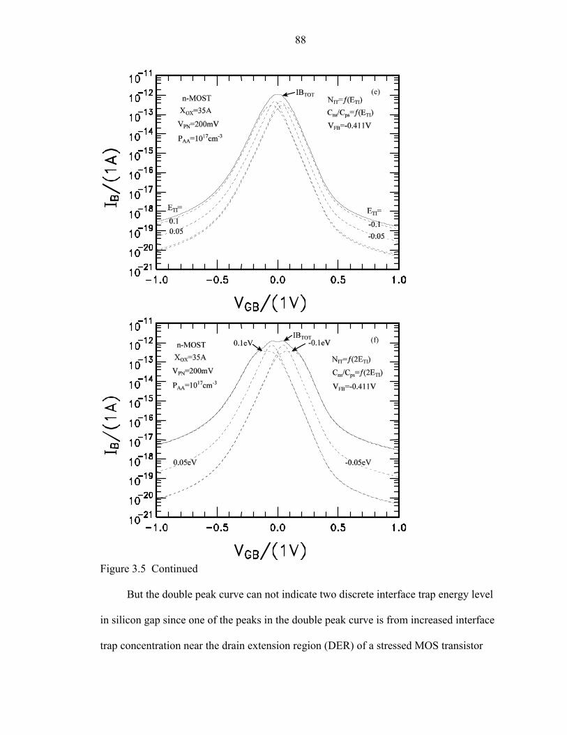
88
Figure 3.5 Continued
But the double peak curve can not indicate two discrete interface trap energy level
in silicon gap since one of the peaks in the double peak curve is from increased interface
trap concentration near the drain extension region (DER) of a stressed MOS transistor
(f)
(e)
89
[26]. As indicated in (2.12b), the spatial interface trap concentration could greatly
increase the shoulder amplitude to form a double peak curve for a MOS transistor with
U-shaped dopant impurity concentration.
Figure 3.5 shows the effect of discrete and mid-gap symmetrical interface trap
energy distribution (with mid-gap) on R-DCIV lineshape. As predicted by the theory in
chapter 2, the peak current IB-peak occurs at the gate voltage VGB-peak or the interface or
surface concentrations of electrons and holes, NS and PS, when cnsNS and cpsPS are equal.
From the unit steady-state recombination rate (2.7a), it is evident that the lineshape is
strongly affected by the emission rates of electrons and holes which in turn are dependent
on the energy level position of the interface traps in the silicon gap. A more direct
representations is given in (2.7b) which explicitly shows the effect of the energy level
position as indicated by the term cosh(UTI*). Ii is not just the energy level position but
also the electron and hole capture rate ratio as indicated by the definition of UTI*,
)4.3()]c/cln(Tk21)EE[(TkUE psnsBITB
*TI
*TI +−==
From the base recombination current equation in (3.2), it is immediately obvious
that there is a plateau in the IB-VGB curves centered at the maximum whose width is
proportional to ETI* as shown in Figure 3.5, such as the curves with interface trap energy
level ETI=±0.45, ±0.40, ±0.35 and ±0.30eV in Fig 3.5(c). Only when the surface energy
band bending or the gate voltage is sufficiently large to make PS>(ens+eps)/cps or
NS>(ens+eps)/cns that the unit steady-state recombination rate RSS1 or the basewell
recombination current IB will start to decrease. For a interface trap level at mid-gap,
(ens+eps)/(cps+cns) is about equal to intrinsic carrier concentration ni. Therefore, this
corresponds to the sharp lineshape centered at the intrinsic surface condition or the
90
subthreshold voltage. But for a shallow interface trap energy level, such as ETI=±0.4,
0.50eV, either ens or eps will be very large since they are assumed to be proportional to
exp(ETI). Therefore, a much larger gate voltage VGB is necessary to increase electron or
hole concentration at surface in order to reduce recombination current IB.
In Figure 3.5 (a), the interface trap energy level ETI=±0.1eV symmetrically
broadens the R-DCIV lineshape. While ETI=±0.2eV give a broadening shoulder on both
side of peak as shown in Figure 3.5(b). Figure 3.5(c) gives the contribution to total
recombination recurrent IB from each interface trap energy level varying from -0.5eV to
+0.5eV with a 0.05eV step. The effect of energy level number of interface traps NETIN
is given in Figure 3.5(d).
The contribution from less than about 11 levels of interface traps, except NETI=1
at mid-gap ETI=0, gives an R-DCIV lineshape with a hump on both shoulders as shown
by these curves labeled NETI=7, 9 and 11 in Figure 3.5(d). Once NETIN is greater than
21 for the interface traps with symmetrically distributed density in Si-gap, the humps
disappear on the shoulders and the total contribution will give a smooth IB-VGB curve,
(curves labeled NETI=21, 101 and 999).
Figure 3.6 shows the comparison among three distributions of interface traps in
silicon gap: (1) a U-shaped DOS with NIT=1010*cosh(ETI/ETIN)cm-2, (2) a constant DOS
NIT=1010cm-2, and (3) a discrete interface trap energy level at mid-gap ETI=0. The
normalized R-DCIV curves are given in Figure 3.6(a) and (b) for linear scale and semilog
scale. The percentage deviations using the curve with interface trap energy ETI=0as
reference is shown in Figure 3.6(c), while %deviations using a constant density of
interface traps as the reference is given in Figure 3.6(d).
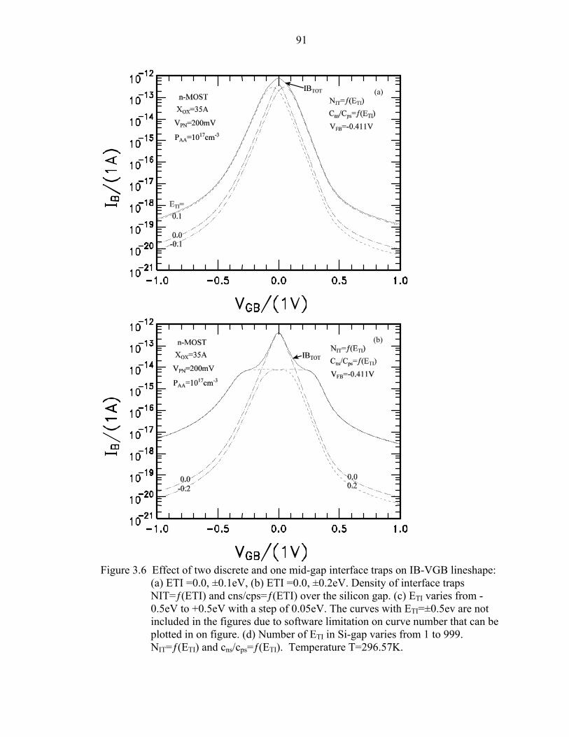
91
Figure 3.6 Effect of two discrete and one mid-gap interface traps on IB-VGB lineshape:
(a) ETI =0.0, ±0.1eV, (b) ETI =0.0, ±0.2eV. Density of interface traps NIT=ƒ(ETI) and cns/cps=ƒ(ETI) over the silicon gap. (c) ETI varies from -0.5eV to +0.5eV with a step of 0.05eV. The curves with ETI=±0.5ev are not included in the figures due to software limitation on curve number that can be plotted in on figure. (d) Number of ETI in Si-gap varies from 1 to 999. NIT=ƒ(ETI) and cns/cps=ƒ(ETI). Temperature T=296.57K.
(b)
(a)
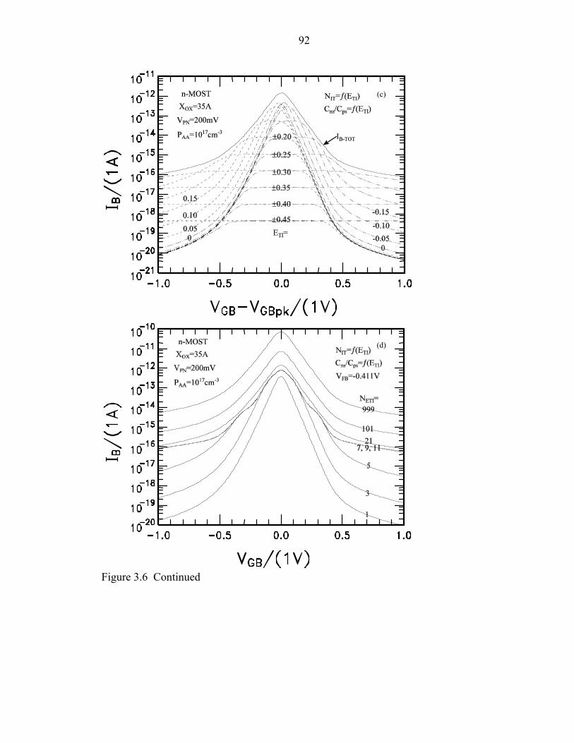
92
Figure 3.6 Continued
(d)
(c)
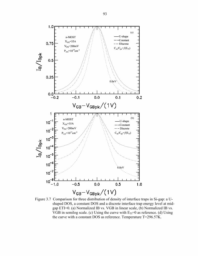
93
Figure 3.7 Comparison for three distribution of density of interface traps in Si-gap: a U-
shaped DOS, a constant DOS and a discrete interface trap energy level at mid-gap ETI=0. (a) Normalized IB vs. VGB in linear scale, (b) Normalized IB vs. VGB in semilog scale. (c) Using the curve with ETI=0 as reference. (d) Using the curve with a constant DOS as reference. Temperature T=296.57K.
(b)
(a)
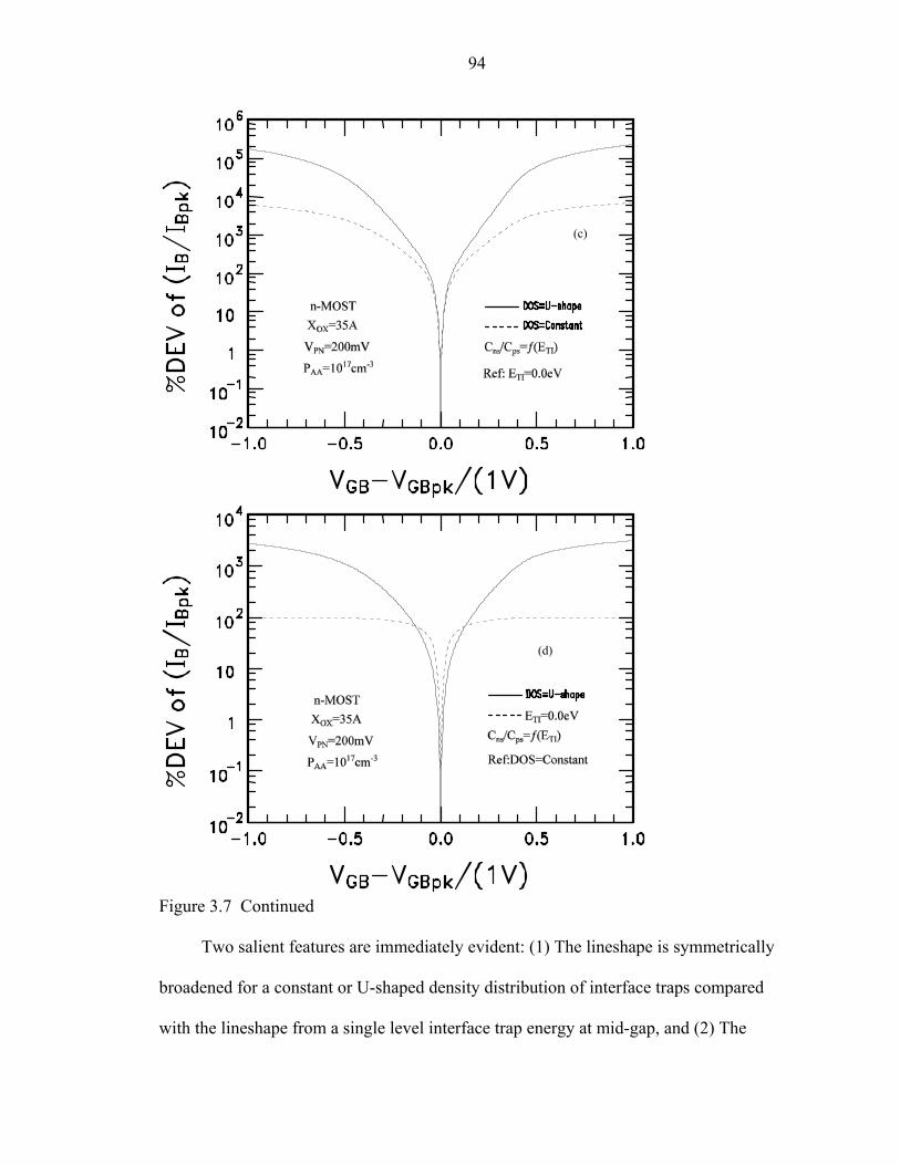
94
Figure 3.7 Continued
Two salient features are immediately evident: (1) The lineshape is symmetrically
broadened for a constant or U-shaped density distribution of interface traps compared
with the lineshape from a single level interface trap energy at mid-gap, and (2) The
(d)
(c)

95
broadening for a U-shaped density distribution of interface traps is greater than a constant
distribution of DOS. These indicated that the lineshape is strongly affected by density of
states for continues density distribution of traps. Thus, the broadened lineshape observed
in experiment R-DCIV data can not only be accounted for by the spatial variation of the
surface concentration of the dopant impurity concentration at the Si-surface under the
SiO2/Si interface, but also by the density distribution of interface traps in silicon gap.
The equation of effective interface trap energy level,
ETI*=ETI+(kT)loge(cns/cps)1/2, is completely independent of the surface energy band
bending and other material properties, such as surface impurity concentrations, oxide
thickness, and carrier capture rates. In modern Si integrated circuit manufacturing
technology, ion implantation has become the principal method for introducing energetic,
charged atoms into a substrate to modify surface properties of materials in order to
accuracy control the electrical characteristics of MOS transistors. According to Slater’s
perturbation theory, the interface trap energy levels are those shifted from the ideal
positions of energy level in both conduction and valence bands into the energy gap, by
localized perturbation of trap potential. The localized perturbations are from the random
variation of bond angle and bond length at the SiO2/Si interface, therefore stain-distorted
Si-Si and Si-O bond can give a perturbation. The beam incident angle, energy, and dose
of ion implantation, HALO implantation step designed to suppress the short channel
effect, and post-implantation high temperature processing step, can also contribute to
perturbations. The larger perturbations or larger changes of bond length and angles, give
deeper trap energy levels, and smaller perturbations are more numerous. Thus, the energy
96
distribution of interface trap density is most likely U-shaped and symmetrically arises
towards to the edge of two energy bands from the mid-gap.
The above analysis on IB-VGB lineshape provides the basis for calculating the
dependence of energy position of interface traps. This study can allow us to extract the
energy distribution of interface traps in silicon gap from the experimental R-DCIV IB-
VGB curves. If energy distribution of interface traps is a single level, we would see R-
DCIV curves with a flat-top in experimental data once the interface trap level is not right
at the midgap. If the energy distribution of interface traps contains several discrete levels,
then DCIV curves with multiple peaks or broad shoulders would appear in the
experimental measurements, which can be analyzed to extract the energy position and
distribution of energy levels. However, all the R-DCIV lineshape so far observed has a
sharp peak in our comprehensively experimental measurements, and we have not
observed any R-DCIV curves with flat-top or double peaks and/or broad shoulders. This
indicates that the contribution from each interface trap energy level, if some discrete level
is present, is washed out by a continue distribution of interface trap levels due to random
bond lengths and angles of Si:Si and Si:O4. The R-DCIV experiment data confirm that
the energy distribution of interface traps is not several discrete energy levels and a most
probable distribution is a U-shaped one in silicon energy gap for modern MOS
transistors. Thus, we should use a U-shaped energy distribution of interface traps to
extract the spatial profiles of the dopant impurity concentration, interface trap
concentration and oxide thickness, instead of using a trap level at mid-gap ETI=0 which
is commonly used or a constant energy distribution of interface traps over the entire
silicon gap.
97
3.4 Temperature Dependence
The MOS-gated structure [7, 8] described here [9, 10, 26] eliminates the
uncertainties during the earlier experiments which attempted to analyze the electrical
characteristics of the field-effect in the p/n junction diode and transistors [65-66], since
the surface potential is exactly known at the surface recombination current peak.
Theoretical analysis shows that the lineshape of R-DCIV curves can be characterized by
three parameters: peak current amplitude IB-peak, gate voltage at the peak VGB-peak,
and the half-width at half-maximum (HWHM). The three parameters are highly sensitive
to the transistor design, such as channel length L and width W, and the spatial variation
of the dopant impurity and interface trap concentrations. Method for extracting dopant
impurity concentration at mid-gap interface trap was demonstrated by Yih Wang [40].
However, the accuracy of the extraction of transistor parameters may be sensitively
dependent on the transistor temperature, which may vary during the experiment
measurements. In the section, we shall investigate the temperature dependence to
ascertain its limitation on the accuracy and resolution of R-DCIV methodology.
It is well-known that the transistor characteristics are temperatures dependent, some
with a power law Tn from the dependence of the electron or hole mobility and diffusivity,
and from other parameters with much stronger temperature dependences due to thermally
activated mechanism, such as the electron and hole emission from a bound state in the
silicon energy gap, with a thermal activation energy as high as EG/2. There are two
reasons to ascertain the temperature dependence of the IB-VGB curves: (1) the transistor
temperature could be controlled to 0.10C accuracy in controlled laboratory experiments
on small chips bonded to a small (~1/8 to 1/4 inch diameter) metal headers in which the
error or uncertainty on the extraction of dopant impurity profile from experimental
98
lineshape data is the prime concern, and (2) in manufacturing applications of R-DCIV
method for profiling, processing, design and reliability monitoring [26] in which, the
sample is an 8-inch to 12-inch diameter silicon disks where temperature cannot be easily
controlled to such precision.
Bludau et al. [32], has modeled the effect of energy gap narrowing with increasing
temperatures for temperature below than 300K as given in (3.6a) and (3.6b). Sah, McNutt
and Chan [5, 6, 33] gave an additional formula for temperatures above 300K, which can
be simplified for temperatures less than 500K as given in (3.6c).
)7.3(])1356/T()2.814/T()64.437/T(1[
T104353.381577.0)m/mm(
)c6.3()TK300(T10800.22080.1)T(E
)b6.3()K300TK150(T1005.3T10025.91785.1)T(E
)a6.3()K150T0(T1005.6T10059.11700.1)T(E
)5.3()Tk2/Eexp()300/T()m/mm(105100.2)T(n
232
32PN
4G
275G
275G
BG2/34/32
PN19
i
)
(
++−
××+=
<×−=
<<×−×−=
<<×−×−=
×=
−
−
−−
−−
The temperature dependence of the intrinsic carrier concentration ni is obtained by
Sah, McNutt and Chan in 1974 [5, 6, 33]. Using the above expressions, they fitted the
theory to extensive data reported in the literature from Boltzmann distribution at low
concentrations or low temperatures, up to the melting point of silicon. We shall use these
formulas.
3.4.1. Temperature Dependence of the Peak Current IB-peak
Temperature dependence of electron-hole recombination at interfacial electronic
traps under the MOS-gated surface channel in the basewell channel region is mainly
determined by the temperature dependence of intrinsic carrier concentration ni in (2.12).
For a single energy level SRH recombination rate at ET-EI from the intrinsic Fermi level
EI, the temperature dependence of peak current IB-peak can be evaluated using the
99
temperature dependence of intrinsic carrier concentration ni and the SRH steady-state
electron-hole recombination rate at the peak, RSS-peak, given by (2.6) and (2.10). For
multi-interface trap levels or U-shaped density of interface traps, the total of RSS-peak is
summed over all the recombination rates from each interface trap level in the silicon gap.
)b8.3(N)Ucosh()2/Uexp(
]Tk/)2/EqVexp[(T
)a8.3(N)Ucosh()2/Uexp(
]1)U[exp(2
n)cc(R
C
VT
E
EEIT*
TIPN
BGPN5.1
IT*TIPN
PNi2/1
psnspeakSS
∑=
−
+−
∝
+−
=
Where, UPN=VPN/kT is the normalized forward bias. The effective interface tap level
ETI* or UTI*is given by (2.9). The dependence of RSS-peak on the trap energy level is
contained in the hyperbolic cosine term, cosh(UTI*) in (3.8). This term is symmetric
around the minimum at UTI*=0 or UT-UI= 0.5*ln(cns/cps) at which the denominator
reaches its minimum value. Thus, RSS-peak is at its maximum. The equation is
completely independent of the surface energy band bending and other material properties,
such as surface impurity concentrations, oxide thickness. The recombination peak current
IB-peak is given by ∫ − dydzR peakSS integrated through the channel length, from y=0 to
y=LCH, between the source and drain junction-space-charge regions, and the channel
width from Z=0 to W. In the denominator of SRH recombination rate, (3.8a) and (3.8b)
there are two terms. One is exp(UPN/2) which is from forward bias at one or more p/n
junctions, the other is cosh(UTI*) which is from effective interface trap energy level. In
the limiting cases, when exp(UPN/2) is much greater than cosh(UTI*) or cosh(UTI*) is
much greater than exp(UPN/2), RSS-peak can be simplified to
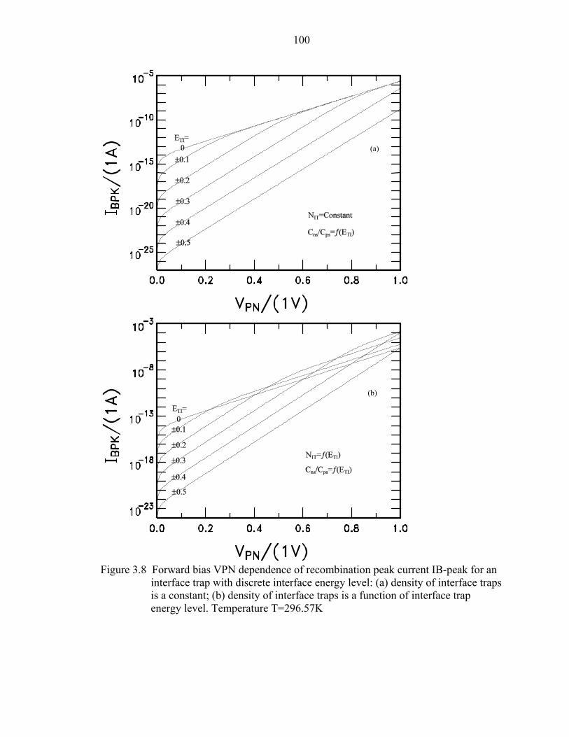
100
Figure 3.8 Forward bias VPN dependence of recombination peak current IB-peak for an
interface trap with discrete interface energy level: (a) density of interface traps is a constant; (b) density of interface traps is a function of interface trap energy level. Temperature T=296.57K
(b)
(a)
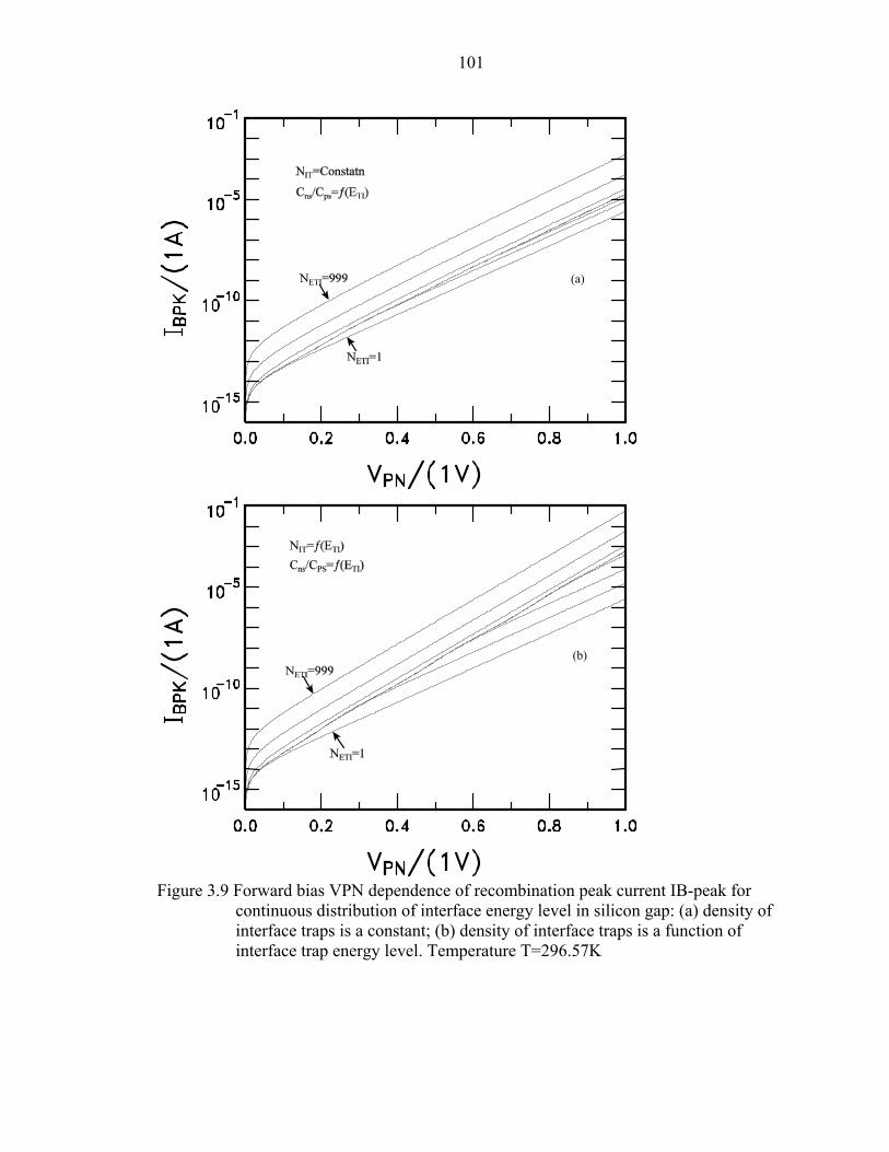
101
Figure 3.9 Forward bias VPN dependence of recombination peak current IB-peak for
continuous distribution of interface energy level in silicon gap: (a) density of interface traps is a constant; (b) density of interface traps is a function of interface trap energy level. Temperature T=296.57K
(b)
(a)
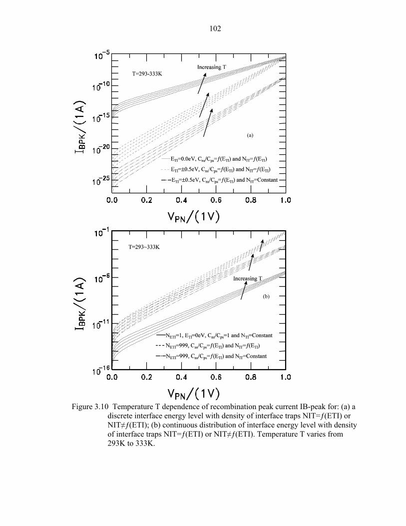
102
Figure 3.10 Temperature T dependence of recombination peak current IB-peak for: (a) a
discrete interface energy level with density of interface traps NIT=ƒ(ETI) or NIT≠ƒ(ETI); (b) continuous distribution of interface energy level with density of interface traps NIT=ƒ(ETI) or NIT≠ƒ(ETI). Temperature T varies from 293K to 333K.
(b)
(a)
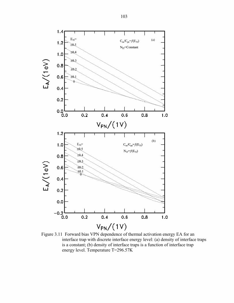
103
Figure 3.11 Forward bias VPN dependence of thermal activation energy EA for an
interface trap with discrete interface energy level: (a) density of interface traps is a constant; (b) density of interface traps is a function of interface trap energy level. Temperature T=296.57K
(b)
(a)

104
ETI=0.0eV, Cns/Cps=ƒ(ETI), NIT=Constant
ETI=±0.5eV,Cns/Cps=ƒ(ETI), NIT=Constant
ETI=±0.5eV, Cns/Cps=ƒ(ETI), NIT=ƒ(ETI)
Increasing T
T=293~333K
Figure 3.12 Temperature T dependence of recombination peak current IB-peak for a discrete interface energy level ETI=0, ±0.5eV, with density of interface traps NIT=ƒ(ETI) or NIT≠ƒ(ETI). Temperature T varies from 293K to 333K.
]Tk/)Eexp[(T
)b9.3()Ucosh()2/Uexp(
]E/ETk/)E2/EqVexp[(T
)a9.3()Ucosh()2/Uexp(
]E/ETk2/)EqVexp[(TR
BA5.1
*TIPN
E
EETINTIB
*TIGPN
5.1
*TIPN
E
EETINTIBGPN
5.1peakSS
C
VT
C
VT
−∝
<<
+−−∝
>>
+−∝
∑
∑
=
=−
For simplicity, we will not consider the temperature effect on density of interface
traps NIT, which is a function of interface trap energy level over silicon gap, i.e.,
NIT=1010× cosh(ETI/ETIN). Here, ETIN is a normalized interface energy value.
105
Equations (3.9a) and (3.9b) show that recombination rate RSS-peak strongly depends on
the temperature due to the large activation energies. Since the ratio of electron and hole
capture rates cns/cps is a function of interface trap energy level ETI, i.e., cns/cps =
ƒ(ETI), we can use the relation to characterize the ETI dependence of RSS-peak. The
forward bias VPN dependence of the activation energy EA of RSS-peak in (3.9a) and
(3.9b) gives several important consequences.
For a discrete and deep interface trap energy level ETI at around the silicon mid-
gap or ETI varying from -0.1eV to +0.1eV, recombination peak current IB-peak and
activation energy EA are essentially proportional to VPN/2 for entire range of forward
bias VPN as shown in Figure 3.7(a) and 3.10(a), at which density of interface traps is a
constant at each interface trap level, and in Figure 3.7(b), and 3.10(b), at which density of
interface traps is a function of interface trap energy level, since exp(UPN/2) is much
greater than cosh(UTI*) in this case.
For an interface trap with a shallow and discrete trap energy level at the near of
conduction and valence bands or ETI varying from ±0.3eV to the edge of two energy
bands, recombination peak current IB-peak and activation energy EA are linearly
proportional to VPN for entire range of forward bias VPN as indicated in (3.9b), since
cosh(UTI*) is much greater than exp(UPN/2) in this case. Again, Curves show the
dependence in Figure 3.7(a), 3.7(b), 3.10(a) and 3.10(b). Density of interface states at
each ET is a constant in silicon energy gap shown as in Figure 3.7(a) and Figure 3.10(a),
while Figure 3.7(b) and Figure 3.10(b) show that density of interface states is a function
of interface trap energy level.
106
When compared with the amplitude of IB-peak from an interface trap with a
constant density of interface states at each ETI, the IB-peak increases on the order of
cosh(ETI/ETIN) for an interface trap at which density of interface states is a function of
ETI. The difference is more pronounced for shallow interface traps, such as the interface
trap level ETI=±0.4eV, and±0.5eV, as shown in Figure 3.7.
For a constant distribution of density of interface traps in silicon energy gap,
recombination peak current IB-peak is exponentially proportional to forward bias VPN/2
as shown in Figure 3.8(a). IB-peak–VPN curve with ETI=0 is essentially parallel to those
curves with constant density of interface states in silicon gap, such as the number of
interface trap level NETI=111 and 999. While, for a U-shape energy distribution of
interface traps, the slope of IB-peak-VPN curve is a little bit higher than that with ETI=0
due to the contribution from the density of states at the interface traps around mid-gap.
The reason for this is that RSS-peak in (3.9a) and (3.9b) is dominated by those interface
traps around the silicon midgap or UTI*≈0 so
that 1])c/c(logTk)EEcosh[()Ucosh( 2/1psnseBIT
*TI ≈+−= . While for those interface
traps with shallower energy level (i.e., ETI≠0), they
have 1])c/c(logTk)EEcosh[()Ucosh( 2/1psnseBIT
*TI >>+−= , which makes RSS-
peak<<1. Thus, these interface trap levels would not significantly contribute to the
amplitude of recombination current. For the same reason, the thermal activation energy
EA has the same forward bias dependence as recombination peak current IB-peak for a
constant density of interface traps or a U-shaped density of interface traps in silicon
energy gap.
107
Experiment data can not uniquely determine the interface trap energy level, which
is measured from the intrinsic Fermi level EI or near silicon mid-gap as defined by
ETI=ET-EI, because the measurement of the amplitude of peak current IB-peak and
thermal activation energy EA only give cosh(UTI*) or the magnitude of ETI*=ETI+
kBTln(cns/cps), but not the sign and not the ratio of electron to hole capture rate at the
trap. The density of interface states would give one more uncertainty factor, normalized
interface trap energy ETIN, if it is a function of interface trap energy level (i.e.,
NIT=ƒ(ETI)). The indetermination has been known in thermal activation measurements
of the DC current due to electron and hole recombination and generation at bulk and
interface traps in two-terminal and multi-terminal semiconductor devices since 1957 [31].
Temperature T can significantly affect recombination peak current IB-peak as
shown in Figure 3.9(a), 3.9(b), 3.12(a) and 3.13(a). The percentage deviation for five
temperatures T=293, 303, 313, 323 and 333K, using the curve with T=296.57K as
reference, are respectively given in Figure 3.12(d) and Figure 3.13(d) for a discrete
interface trap level ETI=0 and a U-shaped distribution of density of interface traps. The
dependence is mainly determined by intrinsic carrier concentration ni, which is a function
T3/2. While, Figure 3.11 shows that temperature has negligible effect on thermal
activation energy EA.
3.4.2. Temperature Dependence of the IB-VGB lineshape
The lineshape of the IB-VGB curve can be characterized by its half-width at half-
maximum (HWHM). The formulae in the accumulation and inversion sides of peak gate
voltage VGB-peak are given in (2.16)
108
)b16.2()siderinsic(int]VVV[V2VV
)a16.2()sideflatband(]VVV[V2VV
peakSSpeakSAASGB
SpeakSpeakSAASGB
−−∆++∆=∆
−∆−−+∆=∆
−−−
−−+
Where, VS-peak is the surface potential at peak current IB-peak, ∆VS is the
variation of surface potential within the ∆VGB range. For the case of an n+ ploy-silicon
gate in an n-MOS transistor with negligible trapped oxide charge, the flat band voltage is
given by
)10.3(Vq2/EV FGFB −−=
VF is majority carrier Fermi potential. In the above equation, dVF/dT arises from
the temperature dependence of the intrinsic carrier concentration ni, which is given by
)11.3(qT2
EdT
dEq21)NN(
dTdNN
qkT
))
kT2Eexp(NN
p(logqk
)))
kT2Eexp(NN
p(logq
kT(dTd
dTdV
GG2/1VCVC
GVC
AAe
GVC
AAe
F
−++
−=
−=
−
For an n-MOS transistor with substrate concentration PAA=1017cm-3 and oxide thickness
XOX=3.5nm, VAA=8.518*10-3V. Thus, the temperature dependence of ∆VGB in (3.9a) and
(3.9b) are dominated by the temperature dependence of ∆VS and other terms can be
ignored
)12.3(qT2
EdT
dEq1)NN(
dTdNN
qkT
))
kT2Eexp(NN
p(logqk
)Vq2/E(dTd
dTdV
dTVd
dTVd
GG2/1VCVC
GVC
AAe
FGFBSGB
−++
−=
+=≈∆
≈∆
−
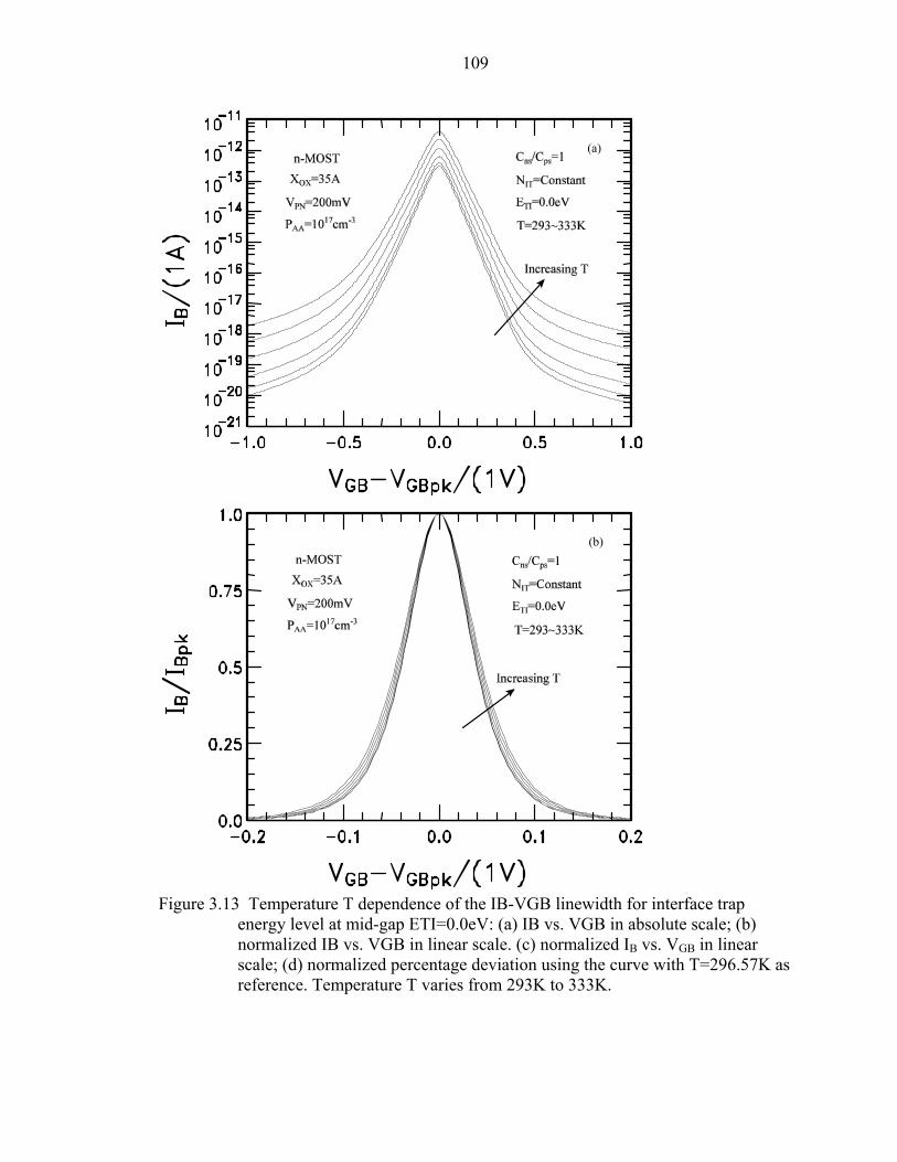
109
Figure 3.13 Temperature T dependence of the IB-VGB linewidth for interface trap
energy level at mid-gap ETI=0.0eV: (a) IB vs. VGB in absolute scale; (b) normalized IB vs. VGB in linear scale. (c) normalized IB vs. VGB in linear scale; (d) normalized percentage deviation using the curve with T=296.57K as reference. Temperature T varies from 293K to 333K.
(b)
(a)
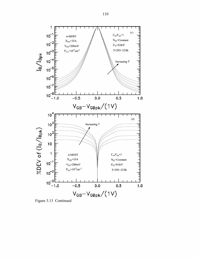
110
Figure 3.13 Continued
(d)
(c)

111
Figure 3.14 Temperature T dependence of the IB-VGB linewidth for a U-shaped
distribution of interface trap energy level in silicon gap: (a) IB vs. VGB in absolute scale; (b) normalized IB vs. VGB in linear scale: (c) normalized IB vs. VGB in linear scale; (d) normalized percentage deviation using the curve with T=296.57K as reference. Temperature T varies from 293K to 333K.
(b)
(a)
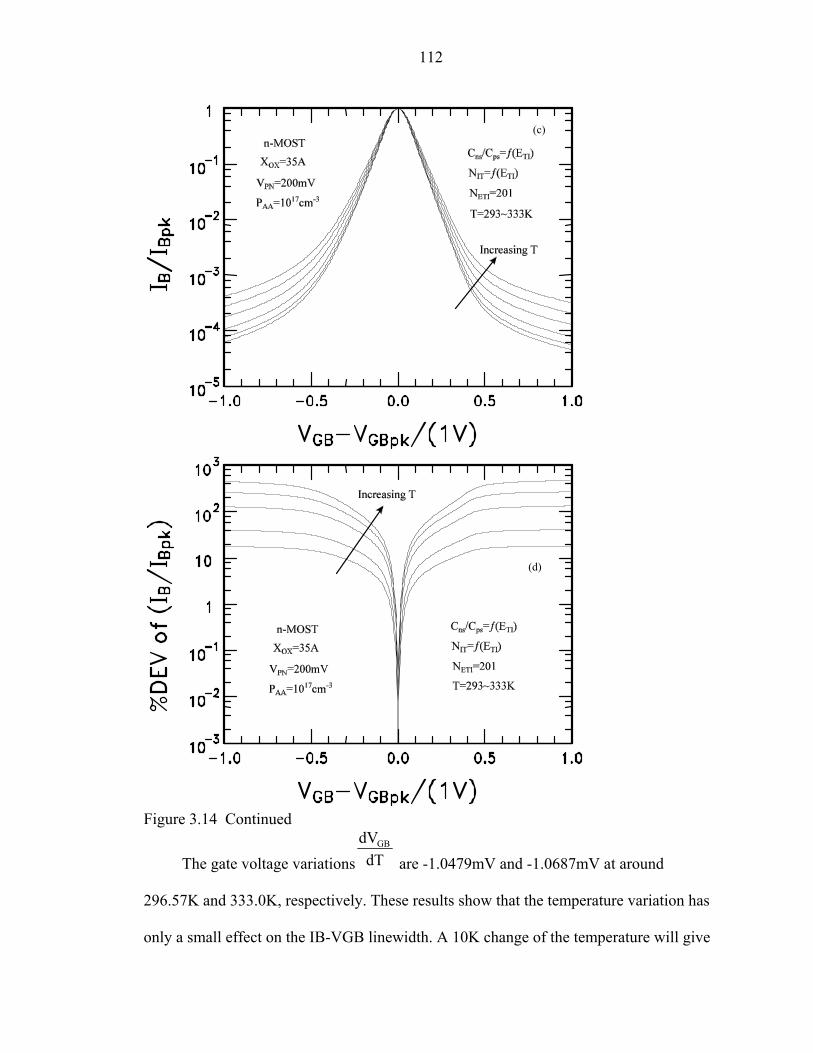
112
Figure 3.14 Continued
The gate voltage variations dTdVGB
are -1.0479mV and -1.0687mV at around
296.57K and 333.0K, respectively. These results show that the temperature variation has
only a small effect on the IB-VGB linewidth. A 10K change of the temperature will give
(d)
(c)
113
only 10mV change in HWHM of IB-VGB curve. Figure 3.12 shows the temperature
effect on R-DCIV lineshape for interface trap level at silicon midgap, while Figure 3.13
gives the temperature effect for a U-shape distribution of interface trap density in silicon
energy gap. For ETI=0.0eV, gate voltage varies from -0.1eV to +0.1eV for peak current
IB-peak down to 10% of the peak as shown in Fig 3.12(d). Using the curve with
temperature T=296.57K as reference, the percentage deviation is less than 10% for the
curves with temperature varying from 293K to 303K. As given in Fig 3.13(d), the
percentage deviation for temperature varying the same range is less than 10% for a U-
shaped energy distribution of interface traps. These results show that the temperature
variation has only a small effect on the IB-VGB linewidth except large temperature
variation. A 10K change of the temperature will give around 10mV change in HWHM of
IB-VGB curve. Thus, the extraction of impurity dopant concentration profile from IB-
VGB lineshape is expected to be rather insensitive to the transistor temperature that
varies during the experimental measurements.
2.4.3. Temperature Dependence of peak gate voltage VGB-peak
The dependence forward bias VPN of the peak gate voltage VGB-peak is another
important characteristics which has been used to determine the flat-band voltage VFB
and average surface dopant impurity concentration PAA-ave=[PAA(x=0, 0<y<L)]AVE
[26]. The accuracy of the extracted PAA-ave may be limited by the temperature
dependence of VGB-peak. Therefore, we shall investigate the temperature effect on
VGB-peak. Since VGB-peak always falls in the flat-band to intrinsic gate voltage range
where electron and hole concentrations are near equal at the interface, i.e., PS=NS, it can
be evaluated from the surface potential VS=VS(VGB) given by
114
)13.3()V()V(VVV 2/1peakS
2/1AApeakSFBpeakGB −−− ++=
VS-peak is the surface potential at peak recombination current IB. VAA =
εSqPAA/2COX2 where PAA is dopant impurity concentration and COX is the oxide
capacitance per unit area. For an MOS transistor, the VS-peak equation is given by
)14.3(2/)VV()c/c(logq/kTV NP2/1
psnsepeakS ++−=−
Substituting (3.14) and (3.12) into (3.13), we obtain the temperature dependence of
VGB-peak equation
)15.3()2/)VV()c/c(log)q/kT(()V(
2/)VV()c/c(log)q/kT(Vq2
EV
2/1NP
2/1psnse
2/1AA
NP2/1
psnseFG
peakGB
++−+
++−−−=−
At high injection levels, the electron and hole concentrations are nearly equal at Si/SiO2
interface, i.e., VP=-VN, and the maximum surface recombination rate is near the flat-
band. As indicated in (3.15), peak gate voltage is mainly determined by four parameters
(1) substrate dopant impurity concentration PAA, (2) gate oxide thickness XOX, (3) emitter
junction forward bias VPN, and (4) the ratio of electron and hole capture rate. For an
nMOS transistor at a given forward bias VPN, a higher dopant impurity concentration PAA
or a thicker gate oxide thickness XOX will shift the peak gate voltage VGB-peak towards a
more positive VGB as shown in Figure 3.14(a) and (b).
Since electron and hole capture rate ratio is a function of interface trap energy level
ETI, i.e., cns/cps= ƒ(ETI), peak gate voltage VGB-peakcns/cps = ƒ(ETI). VGB-peak
value can be used to character the energy distribution of interface traps in silicon energy
gap. At a given VPN, a higher VGB-peak value signifies a higher interface trap energy
level since a higher ratio of cns/cps corresponds to a higher ETI as shown in Figure
3.14(c).
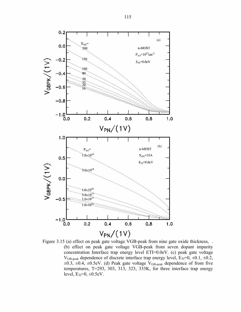
115
Figure 3.15 (a) effect on peak gate voltage VGB-peak from nine gate oxide thickness, .
(b) effect on peak gate voltage VGB-peak from seven dopant impurity concentration Interface trap energy level ETI=0.0eV. (c) peak gate voltage VGB-peak dependence of discrete interface trap energy level, ETI=0, ±0.1, ±0.2, ±0.3, ±0.4, ±0.5eV. (d) Peak gate voltage VGB-peak dependence of from five temperatures, T=293, 303, 313, 323, 333K, for three interface trap energy level, ETI=0, ±0.5eV.
(b)
(a)
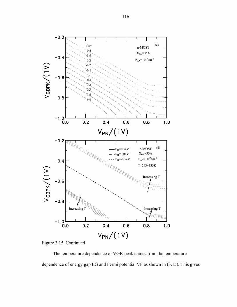
116
Figure 3.15 Continued
The temperature dependence of VGB-peak comes from the temperature
dependence of energy gap EG and Fermi potential VF as shown in (3.15). This gives
(d)
(c)

117
)16.3()2/)VV()c/c(log)q/kT((
)c/c(log)q/k(5.0)V(
)c/c(log)q/k(dTdV
dTdE
q21
dTdV
2/1np
2/1psnse
2/1psnse2/1
AA
2/1psnse
FGpeakGB
++−−
+
−−−=−
Substituting (3.13) into (3.16), we then obtain
)17.3()2/)VV()c/c(log)q/kT((
)c/c(log)q/k(5.0)V(
)c/c(log)q/k(qT2
E)NN(dTdNN
qkT
))
kT2Eexp(NN
p(logqk
dTdE
q1
dTdV
2/1np
2/1psnse
2/1psnse2/1
AA
2/1psnse
G2/1VCVC
GVC
AAe
GpeakGB
++−−
+
−+−
−−−=
−
−
For an interface trap energy level at mid-gap, electron and hole capture rates are
assumed equal, i.e., cns/cps. Thus, the last two term can be dropped in (3.17) since
loge(cns/cps)=0. Then, we have the peak gate voltage variation dVGB-
peak/dT=0.0107mV/K at forward bias VPN=200mV in an n-MOS transistor with
PAA=1017cm-3, XOX=3.7nm and T=296.57K. While for an interface trap energy level
near conduction or valence bands in a transistor with the same parameters, dVGB-
peak/dT are respectively -0.9663mV/K and 0.8185mV/K for ETI=0.5eV and ETI=-
0.5eV. This shows that peak gate voltage VGB-peak has very small temperature
dependence: a 10K change of temperature will give a less than 0.01V shift of VGB-peak
for a discrete interface trap level in the silicon gap. Figure 3.14(d) shows the temperature
dependence of VGB-peak. VGB-peak value for interface trap energy level at mid-gap is
essentially a constant for low injection level for temperature varying from 293K to 333K,
and it shifts towards positive VGB at high injection level for interface trap at mid-gap
ETI=0.0eV. Since IB-VGB lineshape is dominated by those interface trap level close to
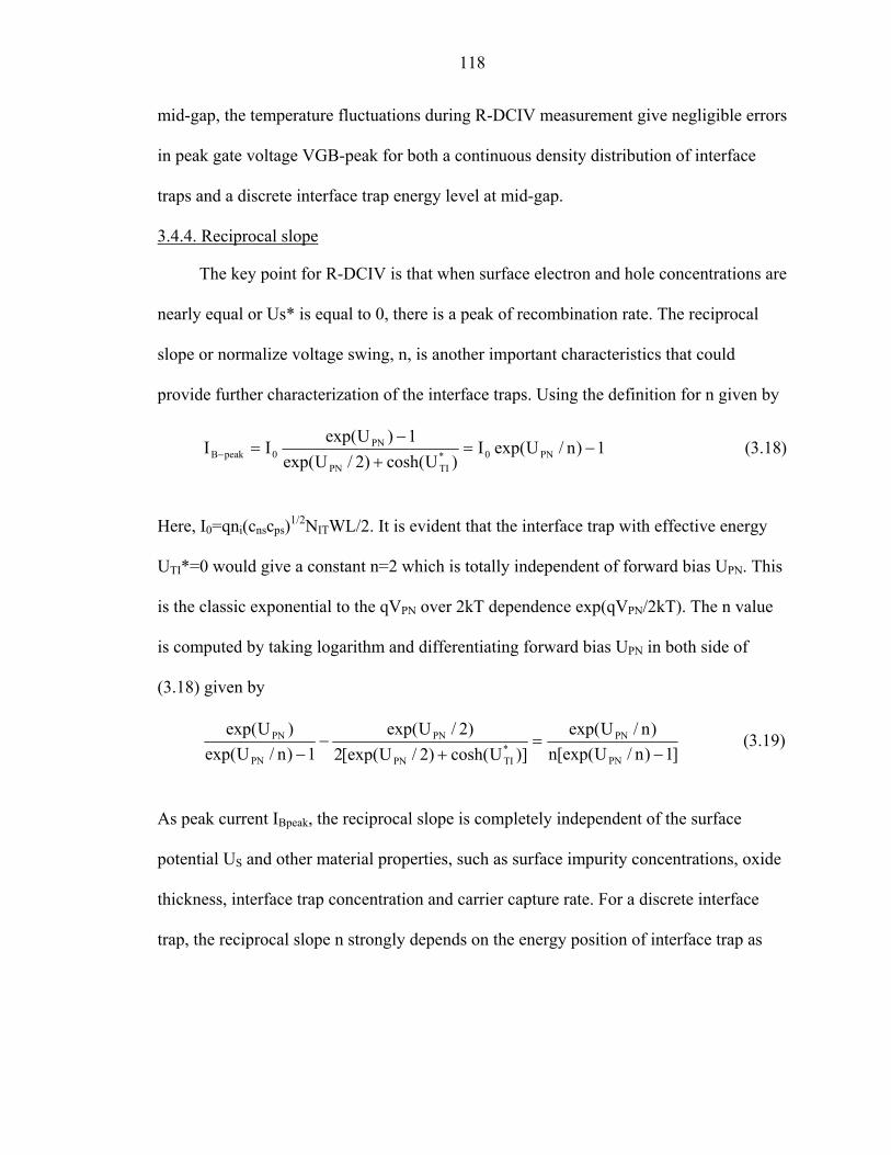
118
mid-gap, the temperature fluctuations during R-DCIV measurement give negligible errors
in peak gate voltage VGB-peak for both a continuous density distribution of interface
traps and a discrete interface trap energy level at mid-gap.
3.4.4. Reciprocal slope
The key point for R-DCIV is that when surface electron and hole concentrations are
nearly equal or Us* is equal to 0, there is a peak of recombination rate. The reciprocal
slope or normalize voltage swing, n, is another important characteristics that could
provide further characterization of the interface traps. Using the definition for n given by
)18.3(1)n/Uexp(I)Ucosh()2/Uexp(
1)Uexp(II PN0*
TIPN
PN0peakB −=
+−
=−
Here, I0=qni(cnscps)1/2NITWL/2. It is evident that the interface trap with effective energy
UTI*=0 would give a constant n=2 which is totally independent of forward bias UPN. This
is the classic exponential to the qVPN over 2kT dependence exp(qVPN/2kT). The n value
is computed by taking logarithm and differentiating forward bias UPN in both side of
(3.18) given by
)19.3(]1)n/U[exp(n
)n/Uexp()]Ucosh()2/U[exp(2
)2/Uexp(1)n/Uexp(
)Uexp(
PN
PN*TIPN
PN
PN
PN
−=
+−
−
As peak current IBpeak, the reciprocal slope is completely independent of the surface
potential US and other material properties, such as surface impurity concentrations, oxide
thickness, interface trap concentration and carrier capture rate. For a discrete interface
trap, the reciprocal slope n strongly depends on the energy position of interface trap as
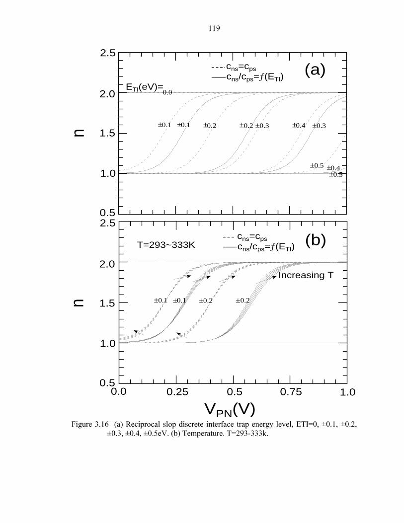
119
cns=cpscns/cps=ƒ(ETI)
0.0
0.1 0.1 0.2 0.2 0.4
0.5 0.40.5
± ± ± ± ±
± ±
±0.3±0.3
±
cns=cpscns/cps=ƒ(ETI)
0.1 0.1 0.2 0.2± ± ± ±
ETI(eV)=
T=293~333K
Increasing T
2.5
2.0
1.5
1.0
0.52.5
2.0
1.5
1.0
0.50.0 1.0
VPN(V)0.25 0.5 0.75
(a)
(b)
nn
Figure 3.16 (a) Reciprocal slop discrete interface trap energy level, ETI=0, ±0.1, ±0.2,
±0.3, ±0.4, ±0.5eV. (b) Temperature. T=293-333k.
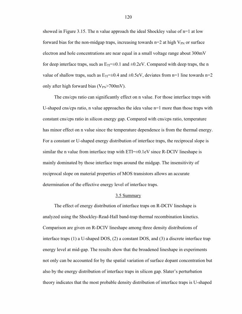
120
showed in Figure 3.15. The n value approach the ideal Shockley value of n=1 at low
forward bias for the non-midgap traps, increasing towards n=2 at high VPN or surface
electron and hole concentrations are near equal in a small voltage range about 300mV
for deep interface traps, such as ETI=±0.1 and ±0.2eV. Compared with deep traps, the n
value of shallow traps, such as ETI=±0.4 and ±0.5eV, deviates from n=1 line towards n=2
only after high forward bias (VPN>700mV).
The cns/cps ratio can significantly effect on n value. For those interface traps with
U-shaped cns/cps ratio, n value approaches the idea value n=1 more than those traps with
constant cns/cps ratio in silicon energy gap. Compared with cns/cps ratio, temperature
has minor effect on n value since the temperature dependence is from the thermal energy.
For a constant or U-shaped energy distribution of interface traps, the reciprocal slope is
similar the n value from interface trap with ETI=±0.1eV since R-DCIV lineshape is
mainly dominated by those interface traps around the midgap. The insensitivity of
reciprocal slope on material properties of MOS transistors allows an accurate
determination of the effective energy level of interface traps.
3.5 Summary
The effect of energy distribution of interface traps on R-DCIV lineshape is
analyzed using the Shockley-Read-Hall band-trap thermal recombination kinetics.
Comparison are given on R-DCIV lineshape among three density distributions of
interface traps (1) a U-shaped DOS, (2) a constant DOS, and (3) a discrete interface trap
energy level at mid-gap. The results show that the broadened lineshape in experiments
not only can be accounted for by the spatial variation of surface dopant concentration but
also by the energy distribution of interface traps in silicon gap. Slater’s perturbation
theory indicates that the most probable density distribution of interface traps is U-shaped

121
in Si-gap. Thus, the extraction spatial profiles of the dopant impurity concentration, the
interface trap concentration, and oxide thickness should use a U-shaped density of
interface traps, instead of using a discrete interface trap level at mid-gap ETI=0 or a
constant energy distribution of interface traps in silicon gap.
Peak current IB-peak has large temperature dependence, while thermal activation
energy EA, IB-VGB lineshape, reciprocal slope n, and peak gate voltage VGB-peak all have
negligible temperature dependence, for both a continuous energy distribution of interface
traps and a discrete interface trap energy level at mid-gap.
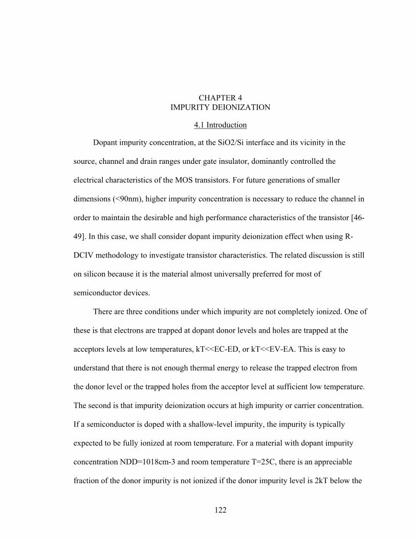
122
CHAPTER 4 IMPURITY DEIONIZATION
4.1 Introduction
Dopant impurity concentration, at the SiO2/Si interface and its vicinity in the
source, channel and drain ranges under gate insulator, dominantly controlled the
electrical characteristics of the MOS transistors. For future generations of smaller
dimensions (<90nm), higher impurity concentration is necessary to reduce the channel in
order to maintain the desirable and high performance characteristics of the transistor [46-
49]. In this case, we shall consider dopant impurity deionization effect when using R-
DCIV methodology to investigate transistor characteristics. The related discussion is still
on silicon because it is the material almost universally preferred for most of
semiconductor devices.
There are three conditions under which impurity are not completely ionized. One of
these is that electrons are trapped at dopant donor levels and holes are trapped at the
acceptors levels at low temperatures, kT<<EC-ED, or kT<<EV-EA. This is easy to
understand that there is not enough thermal energy to release the trapped electron from
the donor level or the trapped holes from the acceptor level at sufficient low temperature.
The second is that impurity deionization occurs at high impurity or carrier concentration.
If a semiconductor is doped with a shallow-level impurity, the impurity is typically
expected to be fully ionized at room temperature. For a material with dopant impurity
concentration NDD=1018cm-3 and room temperature T=25C, there is an appreciable
fraction of the donor impurity is not ionized if the donor impurity level is 2kT below the

123
conduction band edge, EC=ED+2kT since the Fermi level is about 3kT below the
conduction band edge. At the interface SiO2/Si of a MOS transistor, positive gate voltage
can attract electrons to donor traps and negative gate voltage can attract holes to acceptor
traps, even for low dopant impurity concentration. Thus, some dopant impurity atoms
near the interface of SiO2/Si are occupied by electrons at positive gate voltage and some
acceptor impurity atoms are occupied by holes at negative gate voltage. This is the third
deionization condition. Therefore, the ionized impurity density is a function of the
temperature, the dopant concentration or Fermi level and surface potential or gate voltage
in the MOS capacitance structure.
The impurity deionization effect at SiO2/Si interface can occur in two ranges along
the channel in a MOS transistor, the non-compensated range and compensated ranges,
such as n+/p junction range for short channel transistor, as shown in Fig. 4.1 and 4.2,
respectively. The three band diagrams in Figure 4.1 are for N type silicon. The first figure
is for flat-band case. The second band diagram is for accumulation case. In this case, the
positive gate voltage attracts electrons to the SiO2/Si interface. Thus, some electrons are
trapped at the donor impurities near the SiO2/Si interface. In another word, the some
dopant impurities are not completely ionized at positive gate voltage, which is
deionization. The band diagram in Fig. 4.1(c) shows that the negative gate voltage will
push electrons away from the interface in inversion range. Thus, the donor impurities at
the SiO2/Si interface are still ionized at the inversion range.
Fig. 4.2 shows the energy band diagram for compensated ranges. For a short
channel MOS transistor, these ranges are very important since the length of the space
charge range is comparable to channel length. In accumulation case, positive gate
124
Figure 4.1. Impurity deionization effect at the SiO2/Si interface in non-compsated range. (a) Flat-band case, (b) surface at accumulation range, and (c) surface at inversion range.
Figure 4.2. Impurity deionization effect at the SiO2/Si interface in compsated range. (a) Flat-band case, (b) surface at accumulation range, and (c) surface at inversion range.
EC
3.12eV
4.25eV
EF
EV
ED
EFM
EC
EF
EV
ED
EFM
EFM
ECED
(a) Flat-Band (b) Accumulation (c) Inversion
Deionized
Full ionized
EF
EV
EG=1.12eV
VG>0 VG>0
VG<0
(a) Flat-Band (b) Accumulation (c) Inversion
EFM
Deionized
Fully ionized
EC
3.12eV
4.25eV
EF
EV
ED
EFM
EA
EFM
Deionized
Fully ionized
EG=1.12eV
VG=0 VG>0
VG<0
EC
EF
EV
ED
EAEC
EF
EV
ED
EA

125
voltage attracts electrons to interface and push holes away from interface. Thus, some
donor impurities atoms near the SiO2/Si interface are occupied by the electrons and are
deionized while the acceptor impurities are still ionized as shown in Fig. 4.2(b). In
inversion range, gate voltage will push electrons away from interface and attract holes to
interface. Thus, donor impurities are still ionized and acceptor impurities get holes at
interface and are deionized which is illustrated in energy diagram Fig. 4.2(c).
Accounting to energy band diagram in Fig. 4.1 and 4.2, the dopant impurity
deionization effect is entirely negligible except in the strong accumulation region for non-
compensated ranges. While, we shall still consider deionization effect in both
accumulation and inversion ranges, for a moderate doped MOS transistor operating at
room temperature though the inversion will always give better results since impurity
deionization will be less significant in inversion range assuming no measurement related
problems.
Compared with the increase in accuracy gained by switching from Boltzmann
statistics to Fermi statistics, there is a very small gain in accuracy from the switch from
full ionization to deionization models. However, once the temperature is very low and/or
the dopant concentration is very high, deionization effects are not negligible. Also, if the
dopant impurity produces a deep trap level, deionization would become a significant
factor regardless of the doping concentration and/or temperature.
In the chapter, we will investigate the deionization effect dependence on the two
most important device parameters of the MOS transistor: the dopant impurity
concentration PAA and the oxide thickness XOX. As analyses in chapter 2, we will still
use percentage deviation and %RMS deviation of Fermi ionization model to judge
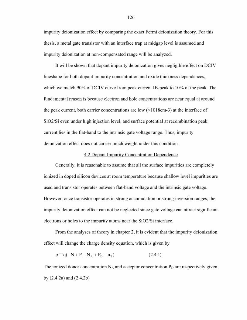
126
impurity deionization effect by comparing the exact Fermi deionization theory. For this
thesis, a metal gate transistor with an interface trap at midgap level is assumed and
impurity deionization at non-compensated range will be analyzed.
It will be shown that dopant impurity deionization gives negligible effect on DCIV
lineshape for both dopant impurity concentration and oxide thickness dependences,
which we match 90% of DCIV curve from peak current IB-peak to 10% of the peak. The
fundamental reason is because electron and hole concentrations are near equal at around
the peak current, both carrier concentrations are low (<1018cm-3) at the interface of
SiO2/Si even under high injection level, and surface potential at recombination peak
current lies in the flat-band to the intrinsic gate voltage range. Thus, impurity
deionization effect does not carrier much weight under this condition.
4.2 Dopant Impurity Concentration Dependence
Generally, it is reasonable to assume that all the surface impurities are completely
ionized in doped silicon devices at room temperature because shallow level impurities are
used and transistor operates between flat-band voltage and the intrinsic gate voltage.
However, once transistor operates in strong accumulation or strong inversion ranges, the
impurity deionization effect can not be neglected since gate voltage can attract significant
electrons or holes to the impurity atoms near the SiO2/Si interface.
From the analyses of theory in chapter 2, it is evident that the impurity deionization
effect will change the charge density equation, which is given by
)1.4.2()nPNPN(q TDA −+−+−ρ=
The ionized donor concentration NA and acceptor concentration PD are respectively given
by (2.4.2a) and (2.4.2b)
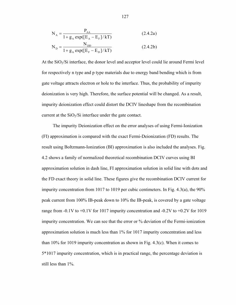
127
)b2.4.2()kT/]EEexp([g1
NN
)a2.4.2()kT/]EEexp([g1
PN
DFA
DDD
FAA
AAA
−+=
−+=
At the SiO2/Si interface, the donor level and acceptor level could lie around Fermi level
for respectively n type and p type materials due to energy band bending which is from
gate voltage attracts electron or hole to the interface. Thus, the probability of impurity
deionization is very high. Therefore, the surface potential will be changed. As a result,
impurity deionization effect could distort the DCIV lineshape from the recombination
current at the SiO2/Si interface under the gate contact.
The impurity Deionization effect on the error analyses of using Fermi-Ionization
(FI) approximation is compared with the exact Fermi-Deionization (FD) results. The
result using Boltzmann-Ionization (BI) approximation is also included the analyses. Fig.
4.2 shows a family of normalized theoretical recombination DCIV curves using BI
approximation solution in dash line, FI approximation solution in solid line with dots and
the FD exact theory in solid line. These figures give the recombination DCIV current for
impurity concentration from 1017 to 1019 per cubic centimeters. In Fig. 4.3(a), the 90%
peak current from 100% IB-peak down to 10% the IB-peak, is covered by a gate voltage
range from -0.1V to +0.1V for 1017 impurity concentration and -0.2V to +0.2V for 1019
impurity concentration. We can see that the error or % deviation of the Fermi-ionization
approximation solution is much less than 1% for 1017 impurity concentration and less
than 10% for 1019 impurity concentration as shown in Fig. 4.3(c). When it comes to
5*1017 impurity concentration, which is in practical range, the percentage deviation is
still less than 1%.
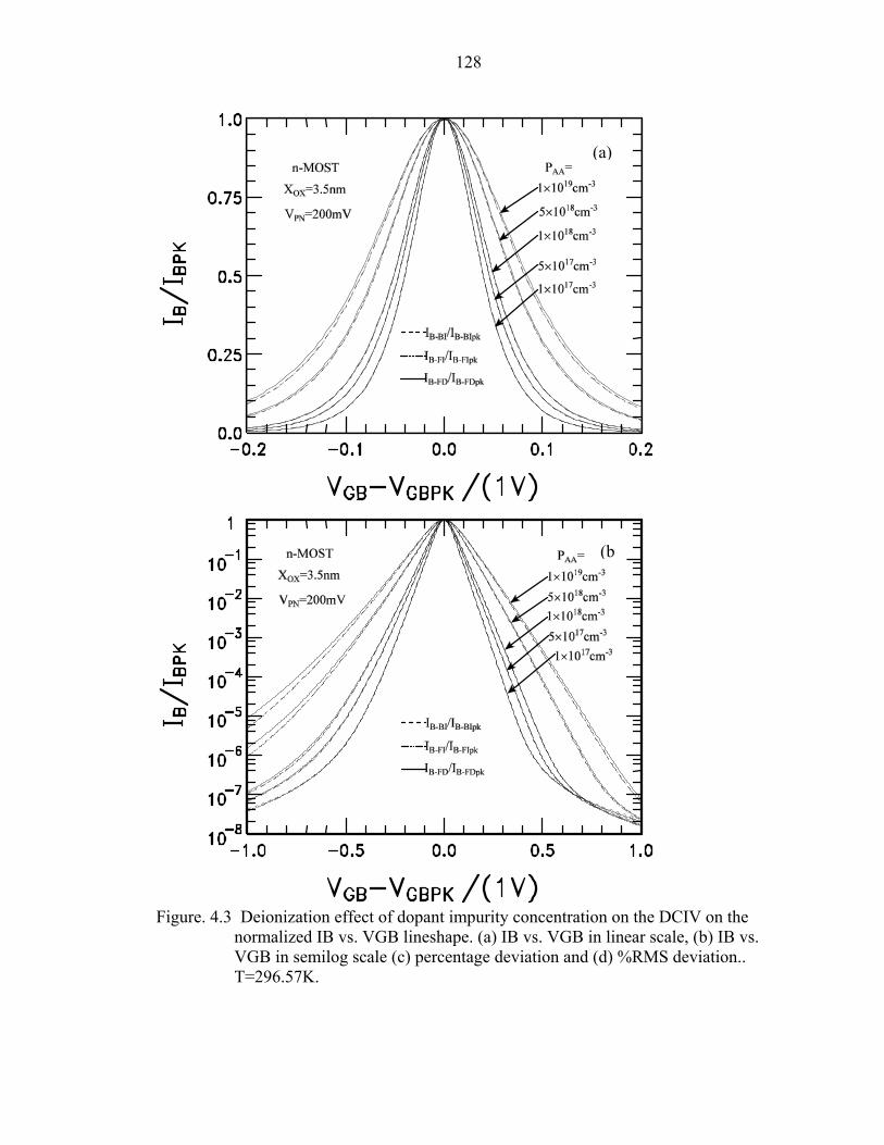
128
Figure. 4.3 Deionization effect of dopant impurity concentration on the DCIV on the
normalized IB vs. VGB lineshape. (a) IB vs. VGB in linear scale, (b) IB vs. VGB in semilog scale (c) percentage deviation and (d) %RMS deviation.. T=296.57K.
(b
(a)
129
Fig.4.3. Continued
Fig. 4.3(d) gives the %RMS deviation by matching the theoretical curve to the
experimental data. We can see that the Fermi-ionization approximation gives less than
4% RMS deviation at 1019 impurity concentration. If impurity concentration is less than
(d
(c)
130
1018cm-3, the %RMS deviation is less than 1% when matching 90% of the theoretical
curve to the experimental data. Once we match 50% DCIV curve from peak current IB-peak
down to 50% of the peak, the %RMS deviation is less than 2 as shown in Fig. 4.3(d).
The value of percentage deviation and %RMS deviation indicates that the surface
impurity deionization is negligible when dopant impurity concentration is in practical
range, such as at around 1018cm-3. From these figures, we can see that the values of
percentage deviation and %RMS deviation of FI are nearly equal to those of BI
approximation solution. The basis reason is that we use FI theory to match the DCIV
curves around the peak current IB-peak, at which surface potential falls between flat-band
and instinct gate voltage. Thus, gate voltage only attracts a very small amount of
electrons or holes to the impurity atoms near the SiO2/Si interface. Thus, impurity
deionization does not carrier more weight than BI approximation solutions.
4.2 Oxide Thickness Dependence
The dimensions of Metal-Oxide-Silicon (MOS) field-effect transistors have
continued to decrease for achieving higher packing density, faster circuit speed and low
power dissipation [1, 67-68]. Aggressive scaling, propelled by the rapid advancement of
VLSI technology, has reduced the oxide thickness at 1.2nm in 2002 [2]. At this scale of
oxide thickness, the surface impurity deionization effect may be negligible since the
increasing electrical field, which is due to the decreasing of oxide thickness for the same
gate voltage, would attract more electrons or holes to impurity atoms near the SiO2/Si
interface.
Figures 4.4 give one family of normalized IB vs. VGB to show the lineshape
dependence on the one of the most basic MOS transistor design parameters, the oxide
thickness. It varies from 10A to 200A, which covers all practical range. For thin oxide
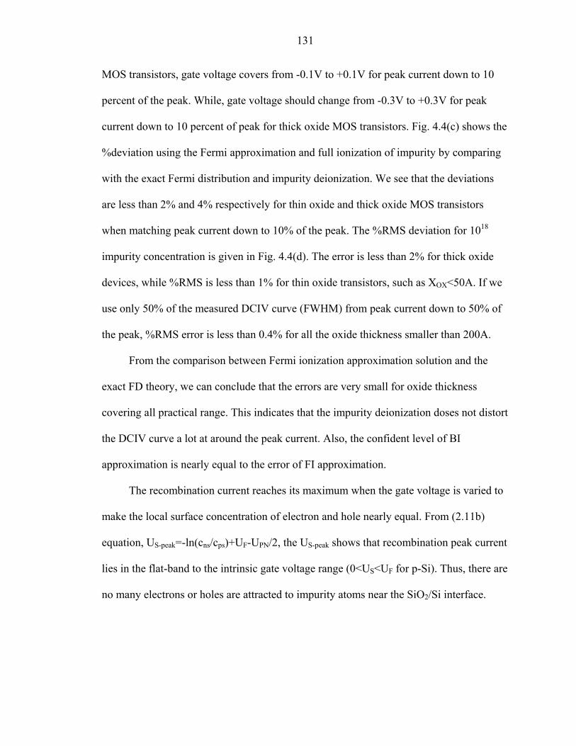
131
MOS transistors, gate voltage covers from -0.1V to +0.1V for peak current down to 10
percent of the peak. While, gate voltage should change from -0.3V to +0.3V for peak
current down to 10 percent of peak for thick oxide MOS transistors. Fig. 4.4(c) shows the
%deviation using the Fermi approximation and full ionization of impurity by comparing
with the exact Fermi distribution and impurity deionization. We see that the deviations
are less than 2% and 4% respectively for thin oxide and thick oxide MOS transistors
when matching peak current down to 10% of the peak. The %RMS deviation for 1018
impurity concentration is given in Fig. 4.4(d). The error is less than 2% for thick oxide
devices, while %RMS is less than 1% for thin oxide transistors, such as XOX<50A. If we
use only 50% of the measured DCIV curve (FWHM) from peak current down to 50% of
the peak, %RMS error is less than 0.4% for all the oxide thickness smaller than 200A.
From the comparison between Fermi ionization approximation solution and the
exact FD theory, we can conclude that the errors are very small for oxide thickness
covering all practical range. This indicates that the impurity deionization doses not distort
the DCIV curve a lot at around the peak current. Also, the confident level of BI
approximation is nearly equal to the error of FI approximation.
The recombination current reaches its maximum when the gate voltage is varied to
make the local surface concentration of electron and hole nearly equal. From (2.11b)
equation, US-peak=-ln(cns/cps)+UF-UPN/2, the US-peak shows that recombination peak current
lies in the flat-band to the intrinsic gate voltage range (0<US<UF for p-Si). Thus, there are
no many electrons or holes are attracted to impurity atoms near the SiO2/Si interface.
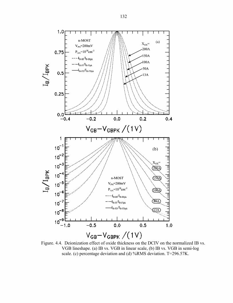
132
Figure. 4.4. Deionization effect of oxide thickness on the DCIV on the normalized IB vs.
VGB lineshape. (a) IB vs. VGB in linear scale, (b) IB vs. VGB in semi-log scale. (c) percentage deviation and (d) %RMS deviation. T=296.57K.
(b)
(a)
133
Fig. 4.4. Continued Therefore, it is reasonable to expect that the percentage deviation and %RMS deviation
of FI approximation are essentially identical to the confident level of BI solutions for the
(d
(c)
134
injected minority carrier concentration, interface trap energy level and temperature
dependences. Also, we can expect that there is a negligible difference between BI and FI
approximation solutions when matching 90% DCIV curve form peak current IB-peak down
to 10% of the peak, for both metal gate and silicon gate MOS transistors. In another
words, the percentage deviation and %RMS deviation of FI approximation confirms that
the simple and time-saving BI approximation solutions can used to extract the dopant
impurity concentration, interface trap concentration, oxide thickness profiles in MOS
transistors in all practical range, including dopant impurity concentration, oxide
thickness, injected minority concentration, interface trap energy level and temperature.
4.4 Summary
Impurity deionization effect of dopant concentration and oxide thickness on DCIV
lineshape has been obtained and presented. From the percentage deviation and %RMS
deviation of Fermi ionization approximation solution, it shows that there is a negligible
impurity deionization near the SiO2/Si interface in MOS transistors when matching 90%
of experimental data from peak current down to 10% of the peak. We can expect that the
errors of FI approximation are nearly identical to the confident level of BI for device
parameters in practical range, such as dopant impurity concentration, oxide thickness,
injected minority concentration, interface trap energy level and temperature, for both
metal gate and silicon gate MOS transistors.
The analyses of impurity deionization confirms that the time-saving and simple
Boltzamann ionization is a good approximation to extract the spatial profiles of device
and material parameter from experiment data, such as the dopant impurity concentration,
interface trap concentration, oxide thickness, since it has a good physical basis at around
the recombination peak current.
135
CHAPTER 5 SUMMARY AND CONCLUSIONS
The success of today’s semiconductor industry can be partially attributed to the
passivation of intrinsic defects at the interface between the silicon channel and the
thermal gate oxide to give extremely low interface trap density in a MOS transistor.
Continued scaling down of the MOS transistor increases the importance of the impurity
distribution along the channel on device’s electrical performance and manufacturing
yield. The increasing importance of understanding the precise impurity concentration
profile have made the experimental determination of impurity profile one of the major
challenges in the development of the next generations of VLSI technology [4, 26], in
order to provide the feedbacks for optimization the design and fabrication. The direct-
current current voltage (DCIV) methodology has the sensitivity to extract the interface
trap and impurity concentration profiles along the surface channel by measuring the gate
bias VGB and the forward junction bias VPN modulated electron-hole recombination
currents at the SiO2/Si interface. This unique sensitivity of DCIV makes it a powerful
tool for monitoring the transistor reliability and for diagnosis of transistor design.
In the previous chapters, fundamental theories which relate DCIV characteristics to
device and material parameters are presented. It is shown that the recombination peak
current, gate voltage at the peak current and DCIV lineshape can be used to extract
device parameters. In order for routine monitoring of surface impurity concentration
profile, interface trap concentration profile and oxide thickness profiles during transistor
fabrication, it is necessary to obtain the confident level of the fast Boltzmann fully

136
ionization solutions. The accuracy of the time-saving and simple BI approximation is
obtained by comparing with the exact Fermi deionization theory showing excellent
accuracy. The fundamental physical basis for high accuracy of the BI approximation to
extract device parameters data is that the electron and hole concentrations are near equal
at around recombination peak current and surface potential at around peak current lies in
flat-band to intrinsic gate voltage. This means that both carrier concentrations near IB-
peak can not be very high even under high injection condition from the forward junction
bias.
The dependence of the confident level or accuracy of the BI approximation on the
dopant impurities concentration PAA, oxide thickness XOX, the injected minority
carriers VPN, energy position of interface trap level ETI and temperature T on the
lineshape of the DCIV IB-VGB curves are computed by matching the exact Fermi
Deionization theory. Results are obtained for both metal gate and silicon gate MOS
transistors. When matching 90% of DCIV curves from the peak current IB-peak down to
%10 of IB-peak, the percentage deviation and %RMS deviation, for metal gate and
silicon gate MOS transistors, are respectively less than 8%, 4% and 10%, 5% when PAA
varying from 1016 to 1019cm-3 with XOX=35A and VPN=200mV; 2%,2% and
4%,2% when XOX varying from 10A to 300A with VPN=200mV and PAA=1018cm-3;
6%, 3% and 10%, 4% for VPN varying from 100 to 800mV with XOX=35A and
PAA=1018cm-;, 8%, 2% and 15%, 5% for ETI varying from 0 to 300mV with
VPN=200mV, XOX=35A, PAA=1018cm-3 and T=296.57. The values are 2%, 1% and
5%, 2% respectively for metal and silicon gate transistors when T varying from 293K to
333K with VPN=200mV, XOX=35A and PAA=1018cm-3 .
137
For a practical MOS transistor with VPN=200mV, XOX=35A, PAA=1018cm-3,
ETI=0 and T=296.57K, the percentage deviation and %RMS deviation are respectively
less than 2%and 1% for metal gate devices, and 4% and 2% for silicon gate transistors
when matching 90% of DCIV curves from peak current down to 10% of the peak using
Boltzmann ionized approximations. These results indicate that the time-saving and
simple BI approximation solutions of R-DCIV methodology are good enough to extract
the spatial profiles of the dopant impurity concentration, interface trap concentration
spatial and oxide thickness along the channel surface in modern MOS transistors.
Three density distributions of interface traps on DCIV lineshape: (1) a U-shaped
DOS, (2) a constant DOS, and (3) a discrete interface trap energy level at mid-gap were
analyzed using the Shockley-Read-Hall band-trap thermal recombination kinetics. One
important result was that the broadened lineshape in experiments can not only be
accounted for the spatial variation of surface dopant concentration but also by the energy
distribution of interface traps in silicon gap. Thus, the parameter profile extraction of
impurity concentration and interface trap concentration, and oxide thickness should use a
U-shaped density of interface traps, instead of using a discrete interface trap level at mid-
gap ETI=0 or a constant energy distribution of interface traps in silicon gap since the
most probable density distribution of interface traps is U-shaped in Si-gap, which is from
random variations of bond length and bond angle of Si-Si and Si-O structures based on
Slater’s perturbation theory.
The ratio of electron and hole captures has a minor effect on the R-DCIV lineshape
for both a single interface trap at mid-gap and a U-shaped distribution of interface trap
energy. R-DCIV lineshape is dominated by those interface traps at around midgap while
138
other interface traps broaden the lineshape at either accumulation or inversion sides. The
analyses of temperature dependence of the peak current, R-DCIV lineshape and peak gate
voltage show that peak current IB-peak has large temperature dependence, while thermal
activation energy EA, IB-VGB lineshape, reciprocal slope n, and peak gate voltage VGB-
peak have negligible temperature dependences, for both a continuous energy distribution
of interface traps and a discrete interface trap energy level at mid-gap.
The comparisons of BI, BD, FI and FD models shows that BI and FI
approximations are respectively found to be nearly as good as BD and FD solutions. The
analyses of impurity deionization effect indicate that deionization will be less significant
in inversion range than in accumulation range assuming no measurement related
problems.
The results of percentage deviation and %RMS deviation of FI approximation
shows that there is a negligible impurity deionization near the SiO2/Si interface in MOS
transistors when matching 90% of experimental data from peak current down to 10% of
the peak. It is reasonable to expect that the errors of FI approximation are nearly identical
to the confident level of BI for all device parameters in practical range, such as dopant
impurity concentration, oxide thickness, injected minority concentration, interface trap
energy level and temperature, for both metal gate and silicon gate MOS transistors.
The analyses of impurity deionization confirms that the time-saving and simple BI
is a good approximation of real phenomenon to extract the spatial profiles of device
parameters from experiment data, such as the dopant impurity concentration, interface
trap concentration and oxide thickness, since it has a good physical basis at around the
recombination peak current.

139
Therefore, the results of the confident level of BI approximation, impurity
deionization effect and distribution of interface trap energy investigated in this
dissertation is expected to be useful for determining the spatial profiles of device
parameters as well as for diagnosis of transistor design in the current and next generations
of semiconductor technologies.

140
APPENDIX ACCURACY OF ITERATIVE ANALYTICAL SOLUTIONS
The Appendix is to test the accuracy of iterative analytical solutions of surface
potential US and the related electron-hole recombination current IB at SiO2/Si interface.
The degeneracy is important in the inversion and accumulation regions of a MOS
transistor, and there is no analytical solution to the Fermi integral. Thus, a full-range
analytical approximation to the Fermi-Integral must be used, such as those shown in
Blackmore’s paper on the subject of F-D integrals [34]. In addition the equation for US is
a transcendental equation, so iterative solution must be employed, such as the rational
Chebyshev approximations [35, 36] used in this thesis. In this appendix, we check the US
and IB accuracy obtained from Boltzmann statistics and fully ionized impurity
approximations.
There are two ways to check the accuracy of these two values of BI approximation
solutions. One is to check them in accumulation and inversion ranges. At these two
ranges, either surface majority carrier concentration or surface minority carrier
concentration dominates in the electric field formula. Thus, we can simplify the formula,
to give an analytical surface potential US formula. Another way is to calculate the surface
potential US and gate voltage VGB from a given recombination current IB.
Accumulation Region
The non-degenerate, fully-ionized solution is simplest when we assume that the
minority carrier terms are negligible and the majority surface concentration is much large
than the bulk concentration. This assumption is somewhat indicative of strong
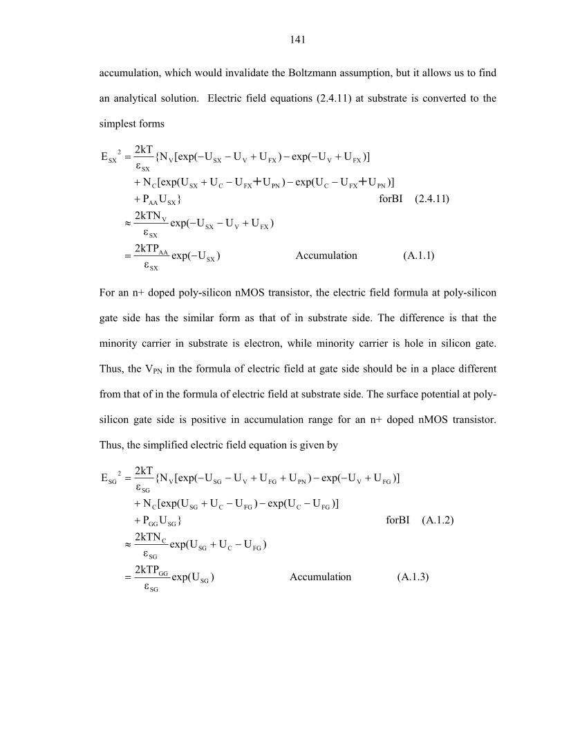
141
accumulation, which would invalidate the Boltzmann assumption, but it allows us to find
an analytical solution. Electric field equations (2.4.11) at substrate is converted to the
simplest forms
)1.1.A(onAccumulati)Uexp(kTP2
)UUUexp(kTN2
)11.4.2(forBIUP)]UUUexp()UUUU[exp(N
)]UUexp()UUU(exp[NkT2E
SXSX
AA
FXVSXSX
V
SXAA
PNFXCPNFXCSXC
FXVFXVSXVSX
2SX
−ε
=
+−−ε
≈
+−−−++
+−−+−−ε
=
++
For an n+ doped poly-silicon nMOS transistor, the electric field formula at poly-silicon
gate side has the similar form as that of in substrate side. The difference is that the
minority carrier in substrate is electron, while minority carrier is hole in silicon gate.
Thus, the VPN in the formula of electric field at gate side should be in a place different
from that of in the formula of electric field at substrate side. The surface potential at poly-
silicon gate side is positive in accumulation range for an n+ doped nMOS transistor.
Thus, the simplified electric field equation is given by
)3.1.A(onAccumulati)Uexp(kTP2
)UUUexp(kTN2
)2.1.A(forBIUP)]UUexp()UUU[exp(N
)]UUexp()UUUU(exp[NkT2E
SGSG
GG
FGCSGSG
C
SGGG
FGCFGCSGC
FGVPNFGVSGVSG
2SG
ε=
−+ε
≈
+−−−++
+−−++−−ε
=
142
Inversion Region
Derivation of the inversion of BI approximation solution is quite similar to that of
accumulation side. The surface minority carrier terms are expected to dominate the
majority carrier terms. Thus, the majority carrier terms are neglected and the sign of
electric field is positive for p-type inversion. Starting with equation (2.4.11), and
neglecting the majority carrier terms, gives
)4.1.A(Inversion)UUexp(P
kTn2
)UUUUexp(kTN2E
SXPNAASX
2i
PNFXCSXSX
C2SX
+ε
=
+−+ε
≈
Similarly, the surface potential at silicon side USG is negative at inversion range,
and the electric field ESG is similar to ESX at accumulation side .What we need to do is
just to change the notations. The electric field is given by
)5.1.A(Inversion)UUexp(P
kTn2
)UUUUexp(kTN2E
PNSGGGSG
2i
PNFGVSGSG
V2SG
+−ε
=
++−−ε
≈
We assume that the oxide charge QOTT, and interface trap charge at gate QITG and at
substrate QITX are zero, the dielectric constants in poly-silicon gate εSG and at substrate
εSX are the same. Thus, the second voltage equation [5] is given by
)6.1.A(EE)QQQE(E
SXSG
OTTITXITGSXSXSGSG
−=⇒+++ε−=ε
For the case of an n+ poly-silicon gate in an nMOS transistor, the surface potential
at poly-silicon gate side USG is in inversion range when the surface potential at substrate
side USX is in accumulation range. From the equations (A.1.1), (A.1.5) and (A.1.6), we
143
have the surface potential at silicon gate side when substrate is in accumulation range
given by
)7.1.A(substrateatonAccumulatiU)PP
nln(UU PNAAGG
2i
SXSG ++=
Note that, in accumulation range, the sign of electric field ESX is negative, the gate
equation (2.4.7) can be transformed into
)8.1.A()C/)Uexp(PkT2(sqrt)PP
nln(q
kTV2V
)7.4.2(C/E)V(signVVVV
2OXSXAASX
AAGG
2i
SXFB
OXSXSXSSGSXFBGB
−ε−++=
ε+++=
Dropping the surface potential term 2VSX, we have the USX at accumulation range given
by
)9.1.A()C
PkT2ln()VV)PP
nln(q
kTVln(2U 2OX
AASXGBPN
AAGG
2i
FBSXε
+−++−≈
Similarly, the surface at poly-silicon side is in accumulation range when surface at
substrate side is in inversion range. The surface potential at poly-silicon side in
inversion range has the same form as in accumulation range given by
)10.1.A(substrateatInversionU)PP
nln(UU PNAAGG
2i
SXSG ++=
In this case, the sign of electric field ES is positive, the gate equation (2.4.7) can be
transformed into
)11.1.A())UUexp(CP
nkT2(sqrtV)PP
nln(q
kTV2V
)7.4.2(C/E)V(signVVVV
SXPN2OXAA
2iSX
PNAAGG
2i
SXFB
OXSXSXSSGSXFBGB
+ε
+++=
ε+++=
+
144
Therefore, we have the surface potential at substrate side when surface is at inversion
range given by
)12.1.A())Uexp(CP
nkT2ln()V)PP
nln(q
kTVVln(2U PN2OXAA
2iSX
PNAAGG
2i
FBGBSXε
−−−−≈
For a metal gate nMOS transistor, the electric field ESG and surface potential USG at gate
side are zero. Following the same procedures, we have the surface potential USX at accumulation
and inversion ranges given by
)14.1.A(Inversion))Uexp(CP
nkT2ln()VVln(2U
)13.1.A(onAccumulati)C/PkT2ln()VVln(2U
PN2OXAA
2iSX
FBGBSX
2OXAASXGBFBSX
ε−−≈
ε+−−≈
Since only one surface potential term VSX is dropped for metal gate case, while
2VSX is dropped for silicon gate case. Consequently, the VSX computation for metal gate
case is more accurate than that of silicon gate case. For the same reason, both results are
close to but not equal to that of iterative computations. The unit Shockley-Read-Hall
steady-state electron-hole recombination rate RSS1, effective surface potential US* and
effect interface trap energy UTI* are given by (2.7b), (2.8b) and (2.9).
)9.2()]c/cln(21Tk/)EE[(Tk/EU
)b8.2(Sipfor2/UU)c/c(logUU
)b7.2()Ucosh()Ucosh()2/Uexp(
]1)U[exp(2
n)cc(R
psnsBITBTI*TI
PNF21
psnses*s
*TI
*sPN
PNi21
psns1SS
+−==
−+−+=
+−
=
The recombination current IB is given by integrating RSS1, through the channel
length from the source to drain junction-space-charge regions, and the channel width
from 0 to W. The analytic solutions can allow us to evaluate the accuracy that of from
iterative computations. The result from iterative computation and analytic solution is
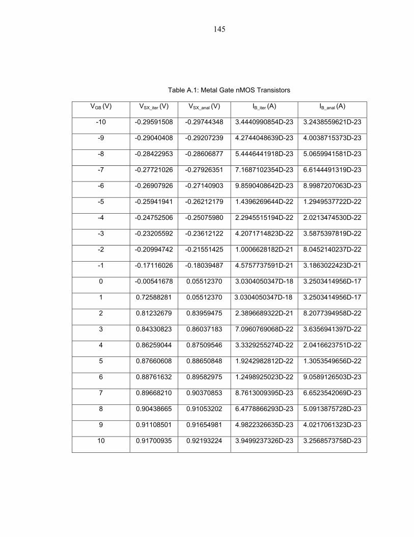
145
Table A.1: Metal Gate nMOS Transistors
VGB (V) VSX_iter (V) VSX_anal (V) IB_iter (A) IB_anal (A)
-10 -0.29591508 -0.29744348 3.4440990854D-23 3.2438559621D-23
-9 -0.29040408 -0.29207239 4.2744048639D-23 4.0038715373D-23
-8 -0.28422953 -0.28606877 5.4446441918D-23 5.0659941581D-23
-7 -0.27721026 -0.27926351 7.1687102354D-23 6.6144491319D-23
-6 -0.26907926 -0.27140903 9.8590408642D-23 8.9987207063D-23
-5 -0.25941941 -0.26212179 1.4396269644D-22 1.2949537722D-22
-4 -0.24752506 -0.25075980 2.2945515194D-22 2.0213474530D-22
-3 -0.23205592 -0.23612122 4.2071714823D-22 3.5875397819D-22
-2 -0.20994742 -0.21551425 1.0006628182D-21 8.0452140237D-22
-1 -0.17116026 -0.18039487 4.5757737591D-21 3.1863022423D-21
0 -0.00541678 0.05512370 3.0304050347D-18 3.2503414956D-17
1 0.72588281 0.05512370 3.0304050347D-18 3.2503414956D-17
2 0.81232679 0.83959475 2.3896689322D-21 8.2077394958D-22
3 0.84330823 0.86037183 7.0960769068D-22 3.6356941397D-22
4 0.86259044 0.87509546 3.3329255274D-22 2.0416623751D-22
5 0.87660608 0.88650848 1.9242982812D-22 1.3053549656D-22
6 0.88761632 0.89582975 1.2498925023D-22 9.0589126503D-23
7 0.89668210 0.90370853 8.7613009395D-23 6.6523542069D-23
8 0.90438665 0.91053202 6.4778866293D-23 5.0913875728D-23
9 0.91108501 0.91654981 4.9822326635D-23 4.0217061323D-23
10 0.91700935 0.92193224 3.9499237326D-23 3.2568573758D-23
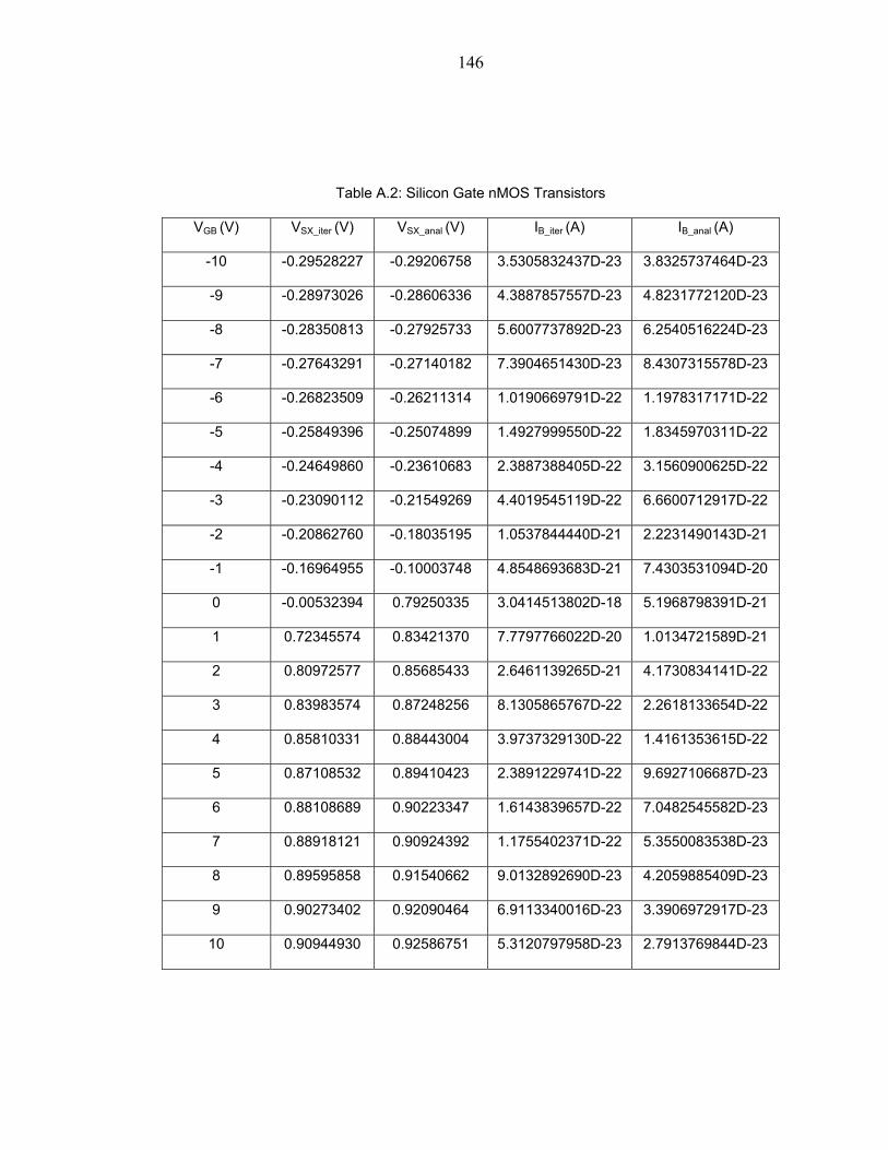
146
Table A.2: Silicon Gate nMOS Transistors
VGB (V) VSX_iter (V) VSX_anal (V) IB_iter (A) IB_anal (A)
-10 -0.29528227 -0.29206758 3.5305832437D-23 3.8325737464D-23
-9 -0.28973026 -0.28606336 4.3887857557D-23 4.8231772120D-23
-8 -0.28350813 -0.27925733 5.6007737892D-23 6.2540516224D-23
-7 -0.27643291 -0.27140182 7.3904651430D-23 8.4307315578D-23
-6 -0.26823509 -0.26211314 1.0190669791D-22 1.1978317171D-22
-5 -0.25849396 -0.25074899 1.4927999550D-22 1.8345970311D-22
-4 -0.24649860 -0.23610683 2.3887388405D-22 3.1560900625D-22
-3 -0.23090112 -0.21549269 4.4019545119D-22 6.6600712917D-22
-2 -0.20862760 -0.18035195 1.0537844440D-21 2.2231490143D-21
-1 -0.16964955 -0.10003748 4.8548693683D-21 7.4303531094D-20
0 -0.00532394 0.79250335 3.0414513802D-18 5.1968798391D-21
1 0.72345574 0.83421370 7.7797766022D-20 1.0134721589D-21
2 0.80972577 0.85685433 2.6461139265D-21 4.1730834141D-22
3 0.83983574 0.87248256 8.1305865767D-22 2.2618133654D-22
4 0.85810331 0.88443004 3.9737329130D-22 1.4161353615D-22
5 0.87108532 0.89410423 2.3891229741D-22 9.6927106687D-23
6 0.88108689 0.90223347 1.6143839657D-22 7.0482545582D-23
7 0.88918121 0.90924392 1.1755402371D-22 5.3550083538D-23
8 0.89595858 0.91540662 9.0132892690D-23 4.2059885409D-23
9 0.90273402 0.92090464 6.9113340016D-23 3.3906972917D-23
10 0.90944930 0.92586751 5.3120797958D-23 2.7913769844D-23
147
given by table A.1 and table A.2 for metal gate and silicon gate case, respectively. In
these two tables, the subscript ‘iter’ means the related values are from iterative
computations, while subscript ‘anal’ means the values are analytical solutions.
The related parameters for an nMOS transistor are that dopant impurity
concentration PAA=1.0*17cm-3, oxide thickness XOX=35A, forward bias VPN=200mV,
flat-band voltage VFB=0.01V, interface trap energy level ETI=0.0V and temperature
T=296.10K. From these two tables, the analytical solutions of surface potential US and
the related recombination current IB are close to those from the iterative computations
since the surface potential term VS was dropped in the gate voltage equation. These
results only check the trend of US and IB in accumulation and inversion regions, but can
not tell us the accuracy of iterative computations.
Now, I will give the second way to check accuracy of iterative computations. In
this method, the recombination current IB is as a known value, which is from iterative
computations. Since every parameter is as a known value in the formula of unit
Shockley-Read-Hall steady-state electron-hole recombination rate RSS1, except parameter
surface potential US. Thus, once we have an IB value, we can calculate the related surface
potential US. From gate voltage equation, given in (2.4.7), we can calculate gate voltage
VGB for metal gate case and VGB-VSG for silicon gate devices once US value is available.
Gate voltage varies from -1.0V to +1.0V for iterative computations in the following two
tables.
The result from iterative computation and analytic solution are given by table A.3 and
table A.4 for metal gate and silicon gate case, respectively. The related parameters are:
Temperature T=296.10K, oxide thickness XOX=35.000A, dopant impurity concentration
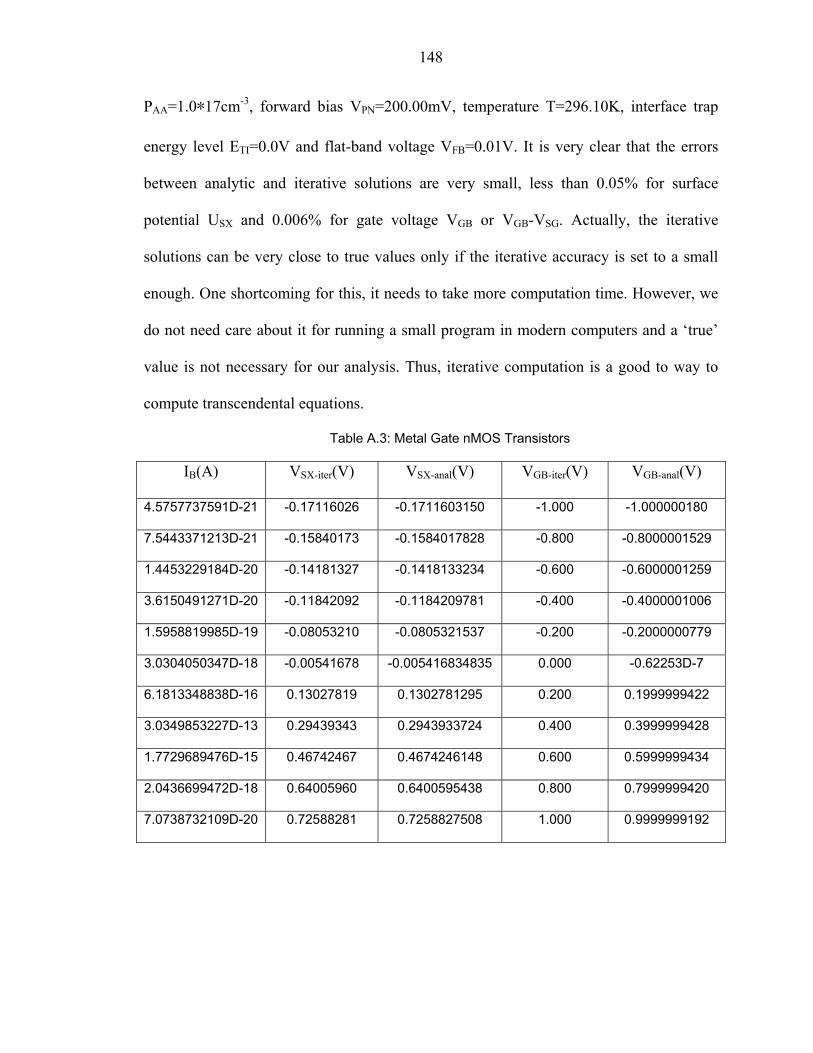
148
PAA=1.0*17cm-3, forward bias VPN=200.00mV, temperature T=296.10K, interface trap
energy level ETI=0.0V and flat-band voltage VFB=0.01V. It is very clear that the errors
between analytic and iterative solutions are very small, less than 0.05% for surface
potential USX and 0.006% for gate voltage VGB or VGB-VSG. Actually, the iterative
solutions can be very close to true values only if the iterative accuracy is set to a small
enough. One shortcoming for this, it needs to take more computation time. However, we
do not need care about it for running a small program in modern computers and a ‘true’
value is not necessary for our analysis. Thus, iterative computation is a good to way to
compute transcendental equations.
Table A.3: Metal Gate nMOS Transistors
IB(A) VSX-iter(V) VSX-anal(V) VGB-iter(V) VGB-anal(V)
4.5757737591D-21 -0.17116026 -0.1711603150 -1.000 -1.000000180
7.5443371213D-21 -0.15840173 -0.1584017828 -0.800 -0.8000001529
1.4453229184D-20 -0.14181327 -0.1418133234 -0.600 -0.6000001259
3.6150491271D-20 -0.11842092 -0.1184209781 -0.400 -0.4000001006
1.5958819985D-19 -0.08053210 -0.0805321537 -0.200 -0.2000000779
3.0304050347D-18 -0.00541678 -0.005416834835 0.000 -0.62253D-7
6.1813348838D-16 0.13027819 0.1302781295 0.200 0.1999999422
3.0349853227D-13 0.29439343 0.2943933724 0.400 0.3999999428
1.7729689476D-15 0.46742467 0.4674246148 0.600 0.5999999434
2.0436699472D-18 0.64005960 0.6400595438 0.800 0.7999999420
7.0738732109D-20 0.72588281 0.7258827508 1.000 0.9999999192
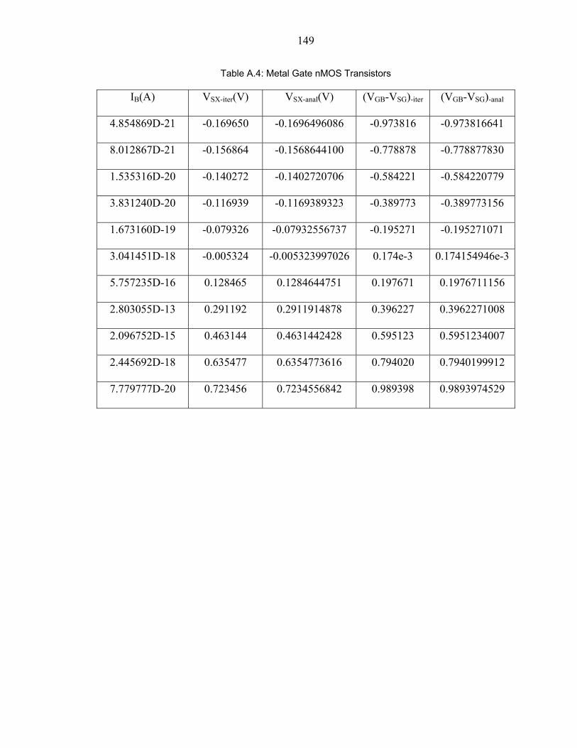
149
Table A.4: Metal Gate nMOS Transistors
IB(A) VSX-iter(V) VSX-anal(V) (VGB-VSG)-iter (VGB-VSG)-anal
4.854869D-21 -0.169650 -0.1696496086 -0.973816 -0.973816641
8.012867D-21 -0.156864 -0.1568644100 -0.778878 -0.778877830
1.535316D-20 -0.140272 -0.1402720706 -0.584221 -0.584220779
3.831240D-20 -0.116939 -0.1169389323 -0.389773 -0.389773156
1.673160D-19 -0.079326 -0.07932556737 -0.195271 -0.195271071
3.041451D-18 -0.005324 -0.005323997026 0.174e-3 0.174154946e-3
5.757235D-16 0.128465 0.1284644751 0.197671 0.1976711156
2.803055D-13 0.291192 0.2911914878 0.396227 0.3962271008
2.096752D-15 0.463144 0.4631442428 0.595123 0.5951234007
2.445692D-18 0.635477 0.6354773616 0.794020 0.7940199912
7.779777D-20 0.723456 0.7234556842 0.989398 0.9893974529
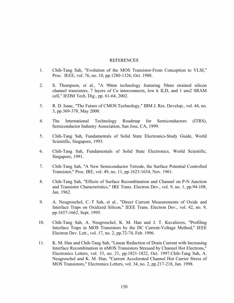
150
REFERENCES
1. Chih-Tang Sah, "Evolution of the MOS Transistor-From Conception to VLSI," Proc. IEEE, vol. 76, no. 10, pp.1280-1326, Oct. 1988.
2. S. Thompson, et al., "A 90nm technology featuring 50nm strained silicon channel transistors, 7 layers of Cu interconnects, low k ILD, and 1 um2 SRAM cell,” IEDM Tech. Dig., pp. 61-64, 2002.
3. R. D. Isaac, "The Future of CMOS Technology," IBM J. Res. Develop., vol. 44, no. 3, pp.369-378, May 2000.
4. The International Technology Roadmap for Semiconductors (ITRS), Semiconductor Industry Association, San Jose, CA, 1999.
5. Chih-Tang Sah, Fundamentals of Solid State Electronics-Study Guide, World Scientific, Singapore, 1993.
6. Chih-Tang Sah, Fundamentals of Solid State Electronics, World Scientific, Singapore, 1991.
7. Chih-Tang Sah, "A New Semiconductor Tetrode, the Surface Potential Controlled Transistor," Proc. IRE, vol. 49, no. 11, pp.1623-1634, Nov. 1961.
8. Chih-Tang Sah, "Effects of Surface Recombination and Channel on P-N Junction and Transistor Characteristics," IRE Trans. Electron Dev., vol. 9, no. 1, pp.94-108, Jan. 1962.
9. A. Neugroschel, C.-T Sah, et al., "Direct Current Measurements of Oxide and Interface Traps on Oxidized Silicon," IEEE Trans. Electron Dev., vol. 42, no. 9, pp.1657-1662, Sept. 1995.
10. Chih-Tang Sah, A. Neugroschel, K. M. Han and J. T. Kavalieros, "Profiling Interface Traps in MOS Transistors by the DC Current-Voltage Method," IEEE Electron Dev. Lett., vol. 17, no. 2, pp.72-74, Feb. 1996.
11. K. M. Han and Chih-Tang Sah, "Linear Reduction of Drain Current with Increasing Interface Recombination in nMOS Transistors Stressed by Channel Hot Electrons," Electronics Letters, vol. 33, no. 21, pp.1821-1822, Oct. 1997.Chih-Tang Sah, A. Neugroschel and K. M. Han, "Current Accelerated Channel Hot Carrier Stress of MOS Transistors," Electronics Letters, vol. 34, no. 2, pp.217-218, Jan. 1998.
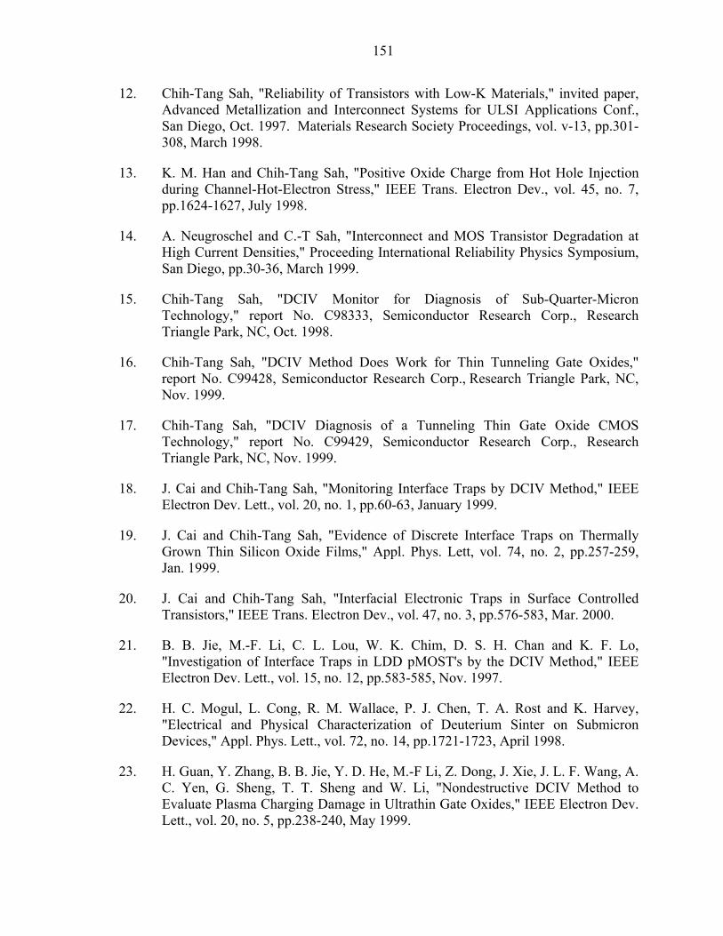
151
12. Chih-Tang Sah, "Reliability of Transistors with Low-K Materials," invited paper, Advanced Metallization and Interconnect Systems for ULSI Applications Conf., San Diego, Oct. 1997. Materials Research Society Proceedings, vol. v-13, pp.301-308, March 1998.
13. K. M. Han and Chih-Tang Sah, "Positive Oxide Charge from Hot Hole Injection during Channel-Hot-Electron Stress," IEEE Trans. Electron Dev., vol. 45, no. 7, pp.1624-1627, July 1998.
14. A. Neugroschel and C.-T Sah, "Interconnect and MOS Transistor Degradation at High Current Densities," Proceeding International Reliability Physics Symposium, San Diego, pp.30-36, March 1999.
15. Chih-Tang Sah, "DCIV Monitor for Diagnosis of Sub-Quarter-Micron Technology," report No. C98333, Semiconductor Research Corp., Research Triangle Park, NC, Oct. 1998.
16. Chih-Tang Sah, "DCIV Method Does Work for Thin Tunneling Gate Oxides," report No. C99428, Semiconductor Research Corp., Research Triangle Park, NC, Nov. 1999.
17. Chih-Tang Sah, "DCIV Diagnosis of a Tunneling Thin Gate Oxide CMOS Technology," report No. C99429, Semiconductor Research Corp., Research Triangle Park, NC, Nov. 1999.
18. J. Cai and Chih-Tang Sah, "Monitoring Interface Traps by DCIV Method," IEEE Electron Dev. Lett., vol. 20, no. 1, pp.60-63, January 1999.
19. J. Cai and Chih-Tang Sah, "Evidence of Discrete Interface Traps on Thermally Grown Thin Silicon Oxide Films," Appl. Phys. Lett, vol. 74, no. 2, pp.257-259, Jan. 1999.
20. J. Cai and Chih-Tang Sah, "Interfacial Electronic Traps in Surface Controlled Transistors," IEEE Trans. Electron Dev., vol. 47, no. 3, pp.576-583, Mar. 2000.
21. B. B. Jie, M.-F. Li, C. L. Lou, W. K. Chim, D. S. H. Chan and K. F. Lo, "Investigation of Interface Traps in LDD pMOST's by the DCIV Method," IEEE Electron Dev. Lett., vol. 15, no. 12, pp.583-585, Nov. 1997.
22. H. C. Mogul, L. Cong, R. M. Wallace, P. J. Chen, T. A. Rost and K. Harvey, "Electrical and Physical Characterization of Deuterium Sinter on Submicron Devices," Appl. Phys. Lett., vol. 72, no. 14, pp.1721-1723, April 1998.
23. H. Guan, Y. Zhang, B. B. Jie, Y. D. He, M.-F Li, Z. Dong, J. Xie, J. L. F. Wang, A. C. Yen, G. Sheng, T. T. Sheng and W. Li, "Nondestructive DCIV Method to Evaluate Plasma Charging Damage in Ultrathin Gate Oxides," IEEE Electron Dev. Lett., vol. 20, no. 5, pp.238-240, May 1999.
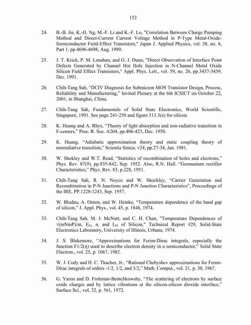
152
24. B.-B. Jie, K.-H. Ng, M.-F. Li and K.-F. Lo, "Correlation Between Charge Pumping Method and Direct-Current Current Voltage Method in P-Type Metal-Oxide-Semiconductor Field-Effect Transistors," Japan J. Applied Physics, vol. 38, no. 8, Part 1, pp.4696-4698, Aug. 1999.
25. J. T. Krick, P. M. Lenahan, and G. J. Dunn, "Direct Observation of Interface Point Defects Generated by Channel Hot Hole Injection in N-Channel Metal Oxide Silicon Field Effect Transistors," Appl. Phys. Lett., vol. 59, no. 26, pp.3437-3439, Dec. 1991.
26. Chih-Tang Sah, “DCIV Diagnosis for Submicron MOS Transistor Design, Process, Reliability and Manufacturing,” Invited Plenary at the 6th ICSICT on October 22, 2001, in Shanghai, China.
27. Chih-Tang Sah, Fundamentals of Solid State Electronics, World Scientific, Singapore, 1991. See page 241-250 and figure 313.3(a) for silicon.
28. K. Huang and A. Rhys, “Theory of light absorption and non-radiative transition in F-centers,” Proc. R. Soc. A204, pp.406-423, Dec. 1950.
29. K. Huang, “Adiabatic approximation theory and static coupling theory of nonradiative transition,” Scientia Sinica, v24, pp.27-34, Jan. 1981.
30. W. Shokley and W.T. Read, “Statistics of recombination of holes and electrons,” Phys. Rev. 87(9), pp.835-842, Sep. 1952. Also, R.N. Hall. “Germanium rectifier Characteristics,” Phys. Rev. 83, p.228, 1951.
31. Chih-Tang Sah, R. N. Noyce and W. Shockley, “Carrier Generation and Recombination in P-N Junctions and P-N Junction Characteristics”, Proceedings of the IRE, PP.1228-1243, Sep. 1957.
32. W. Bludau, A. Onton, and W. Heinke, “Temperature dependence of the band gap of silicon,” J. Appl. Phys., vol. 45, p. 1846, 1974.
33. Chih-Tang Sah, M. J. McNutt, and C. H. Chan, "Temperature Dependences of √(mNmP)/m, EG, ni and LD of Silicon," Technical Report #29, Solid-State Electronics Laboratory, University of Illinois, Urbana, 1974.
34. J. S. Blakemore, “Approximations for Ferim-Dirac integrals, especially the function F1/2(η) used to describe electron density in a semiconductor,” Solid State Electron., vol. 25, p. 1067, 1982.
35. W. J. Cody and H. C. Thacher, Jr., “Rational Chebyshev approximations for Fermi-Dirac integrals of orders -1/2, 1/2, and 3/2,” Math. Comput., vol. 21, p. 30, 1967.
36. G. Yaron and D. Frohman-Bentchkowshy, “The scattering of electrons by surface oxide charges and by lattice vibrations at the silicon-silicon dioxide interface,” Surface Sci., vol, 32, p. 561, 1972.
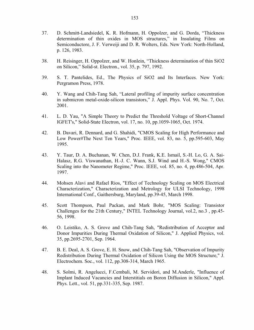
153
37. D. Schmitt-Landsiedel, K. R. Hofmann, H. Oppolzer, and G. Dorda, “Thickness determination of thin oxides in MOS structures,” in Insulating Films on Semiconductore, J. F. Verweiji and D. R. Wolters, Eds. New York: North-Holland, p. 126, 1983.
38. H. Reisinger, H. Oppolzer, and W. Honlein, “Thickness determination of thin SiO2 on Silicon,” Solid-st. Electron., vol. 35, p. 797, 1992.
39. S. T. Pantelides, Ed., The Physics of SiO2 and Its Interfaces. New York: Pergramon Press, 1978.
40. Y. Wang and Chih-Tang Sah, “Lateral profiling of impurity surface concentration in submicron metal-oxide-silicon transistors,” J. Appl. Phys. Vol. 90, No. 7, Oct. 2001.
41. L. D. Yau, "A Simple Theory to Predict the Threshold Voltage of Short-Channel IGFET's," Solid-State Electron, vol. 17, no. 10, pp.1059-1065, Oct. 1974.
42. B. Davari, R. Dennard, and G. Shahidi, "CMOS Scaling for High Performance and Low Power#The Next Ten Years," Proc. IEEE, vol. 83, no. 5, pp.595-603, May 1995.
43. Y. Taur, D. A. Buchanan, W. Chen, D.J. Frank, K.E. Ismail, S.-H. Lo, G. A. Sai-Halasz, R.G. Viswanathan, H.-J. C. Wann, S.J. Wind and H.-S. Wong," CMOS Scaling into the Nanometer Regime," Proc. IEEE, vol. 85, no. 4, pp.486-504, Apr. 1997.
44. Mohsen Alavi and Rafael Rios, "Effect of Technology Scaling on MOS Electrical Characterization," Characterization and Metrology for ULSI Technology, 1998 International Conf., Gaithersburg, Maryland, pp.39-45, March 1998.
45. Scott Thompson, Paul Packan, and Mark Bohr, "MOS Scaling: Transistor Challenges for the 21th Century," INTEL Technology Journal, vol.2, no.3 , pp.45-56, 1998.
46. O. Leistiko, A. S. Grove and Chih-Tang Sah, "Redistribution of Acceptor and Donor Impurities During Thermal Oxidation of Silicon," J. Applied Physics, vol. 35, pp.2695-2701, Sep. 1964.
47. B. E. Deal, A. S. Grove, E. H. Snow, and Chih-Tang Sah, "Observation of Impurity Redistribution During Thermal Oxidation of Silicon Using the MOS Structure," J. Electrochem. Soc., vol. 112, pp.308-314, March 1965.
48. S. Solmi, R. Angelucci, F.Cembali, M. Servidori, and M.Anderle, "Influence of Implant Induced Vacancies and Interstitials on Boron Diffusion in Silicon," Appl. Phys. Lett., vol. 51, pp.331-335, Sep. 1987.

154
49. Y. M. Kim, G. Q. Lo, H. kinoshita, D. L. Kwong, H. H. Tseng, and R.Hance, "Roles of Extended Defect Evolution on the Anomalous Diffusion of Boron in Si During Rapid Thermal Annealing," J. Electrochem. Soc., vol. 138, pp.1122-1130, April 1991.
50. Tomas Diaz de Rubia, Ed., "Defects and Diffusion in Silicon Processing, "MRS Symposia Proceedings, No. 469, Pittsburgh, 1997.
51. B. Sadigh, T. J. Lenosky, S. K. Theiss, Maria-Jose Caturla, Tomas Diaz de Rubia, and M. A. Foad, "Mechanism of Boron Diffusion in Silicon: An Ab Initio and Kinetic Monte Carlo Study," Phys. Rev. Lett., vol. 83, no. 21, pp.4341-4344, Nov. 1999.
52. W. B. Joyce and R. W. Dixon, “Analytic approximations for the Fermi energy of an idea Fermi gas,” Appl. Phys. Let., vol. 31, p. 354, 1977.
53. X. Ayerich-Humet, F. Serra-Mestres, and J. Millan, “An analytical approximation for the Fermi-Dirac integral F3/2(η),” Solid-st. Electron., vol 24, p. 981, 1981.
54. P. Van Hanlen and D. L. Pulfrey, “Accurate, short series approximations to Fermi-Dirac integrals of order -1/2, 1/2, 3/2, 2, 5/2, 3, and 7/2,” J. Appl. Phys., vol. 57, p. 5271, 1985. Erratum, vol. 59, p. 2264, 1986.
55. T. Y. Chang and A. Izabelle, “Full range analytic approximations for Fermi energy and Fermi-Dirac integral F-1/2(η) in terms of F1/2(η),”J. Appl. Phys., vol.65, p. 216, 1989.
56. Chih-Tang Sah, “Insulating layers on silicon substrate,” Properties of Silicon, EMIS Datareviews series No. 4, section 17.1-17.4, pp.497-531, INSPEC, IEE, 1988.
57. Chih-Tang Sah, Fundamentals of Solid-State Electronics-Solution Manual, Section 912, p. 107-108, World Scientific-Singapore, 1996.
58. W. E. Meyerhof, “Contact Potential Difference in Silicon Crystal Rectifiers,” Phys. Rev. vol. 71, p. 727-735. May. 1947.
59. J. Bardeen, “Surface States and Rectification at a Metal Semi-Conductor Contact,” Phys. Rev. vol. 71, p. 717-727, May. 1947.
60. W. Shockley and G. L. Pearson, “Modulation of Conductance of Thin Films of Semi-Conductors by Surface Charges,” Phys. Rev. vol. 74, p. 232–233, Jul. 1948
61. Chih-Tang Sah, Theory of the Metal Oxide Semiconductor Capacitor, technical report no.1, Solid State Electronics Laboratory, University of Illinois, Dec. 1964.
62. Y. Nishi, “Study of Silicon-Silicon Dioxide Structure by Electron Spin Resonance I,” Japan. J. Appl. Phys., vol. 10, pp. 52-62, Jan. 1971.
155
63. J. C. Slater, Insulators Semiconductors and Metals Quantum Theory of Molecules and Solids, vol.3, McGRAW-Hill Book Company, 1967. See Wave Functions of Impurity Atoms at Appendix 2.
64. J. Cai and Chih-Tang Sah, “DCIV Diagnosis for Submicron MOS Transistor Designs and Fabrication Process,” To be published.
65. A. S. Grove and D. J. Fitzgerald, “Surface effects on P-N junctions: Characteristics of surface space-charge regions under nonequilibrium conditions,” Solid-St. Electron., vol.9, pp.783-805, 1966.
66. M. W. Hillen and J. Holsbrink, “The base current recombination at the oxided silicon surface,” Solid-St. Electron., vol.26, no. 5, pp.453-563, 1983.
67. R. H. Dennard, F. H. Gaensslen, H.-N. Yu, V. L. Rideout, E. Bassous, and A. R. LeBlanc, "Design of Ion-Implanted MOSFET's with Very Small Physical Dimensions," IEEE J. Solid-State Circuits, vol. 9, no. 5, pp.256-268, Oct. 1974.
68. J. T. Clemens, "Silicon Microelectronics Technology," Bell Labs Technical Journal, vol. 2, no. 4, pp.76-102, 1997.
69. S. Walstra and C.-T. Sah, “Thin oxide thickness extrapolation from capacitance-voltage measurements,” IEEE Electron Dev. Lett., vol. 44, no. 7, pp.1136-1142, Jul. 1997.
156
BIOGRAPHICAL SKETCH
Zuhui Chen was born in Fujian, China, on October 7, 1973. He received the
Bachelor of Science degree in physics in 1998 from Fujian Normal University and the
Master of Science degree in physics in 2001 from Xiamen University, China. Since the
fall of 2002, he has been studying in Electrical and Computer Engineering at the
University of Florida. He is currently working toward his Ph.D. under the guidance of
Professor Chih-Tang Sah. His Ph.D. dissertation research concerns investigation of
theoretical limitations of recombination DCIV methodology for characterization of MOS
transistors.