investigation of graphene based miniaturized terahertz …...
TRANSCRIPT
Full Length Article
Investigation of graphene based miniaturized terahertz antenna fornovel substrate materialsRajni Bala *, Anupma MarwahaDepartment of ECE, SLIET Longowal, Punjab, India
A R T I C L E I N F O
Article history:Received 2 April 2015Received in revised form9 July 2015Accepted 3 August 2015Available online 23 October 2015
Keywords:GrapheneSubstrate materialsMiniaturized patch antennaTerahertz regimeHFSS
A B S T R A C T
The selection of appropriate substrate material acts as a performance regulator for miniaturized graphenepatch antenna. The substrate material not only controls the transport properties of graphene but alsoinfluences the resonant properties of the graphene patch antenna. The edge fed microstrip line graphenebased rectangular patch antenna is designed here for operating in the frequency range 2.67–2.92 THzfor wireless applications. The performance is investigated for silicon nitride, aluminum oxide, boron nitride,silica and quartz substrate materials on the basis of return loss, voltage standing wave ratio (VSWR), ab-sorption cross section, bandwidth and radiation efficiency. The comparison of results shows that siliconnitride exhibits overall excellent performance by the virtue of having higher bandwidth and radiationefficiency as compared to other chosen substrate materials.
Copyright © 2015, The Authors. Production and hosting by Elsevier B.V. on behalf of KarabukUniversity. This is an open access article under the CC BY-NC-ND license (http://creativecommons.org/
licenses/by-nc-nd/4.0/).
1. Introduction
Graphene material exhibits numerous attractive pure multi-physics, electrical [1] and mechanical properties [2]. These propertiescoupled with CMOS compatibility promise smart miniaturized systemswhich are highly useful in wireless communications. CMOS com-patible microwave graphene based patch antennas, still at theirinfancy, assure extremely low noise and high speed communica-tions [3]. Moreover, the carrier concentration and chemical potentialin graphene based patch antennas can be adjusted through biasvoltage which results in tunable characteristics highly desirable forelectromagnetic applications [4]. Currently research is being carriedout reporting various new materials which can be placed as sub-strates for the graphene patch antenna, as it has been observed thatutilization of novel substrate materials on graphene antenna is notyet abundant and confined to simple materials like silicon [5,6], silicondioxide, quartz [7], polyamide [8], duroid [9], etc. The initial studyusing graphene in antenna at microwaves was presented in 2012,which consisted of a graphene patch over a dielectric silicon sub-strate (εr = 11.2) with thickness of 1 μm. The authors were able toconfirm that the antenna resonant frequency is decreased, virtuallyconsistent with the theoretical model at 0.5 THz, which is indepen-dent of the substrate size [6]. A second important observation is thatas the value of dielectric constant increases, the surface wave losses
should increase and hence decrease the radiation efficiency.Tamagnone et al. [10] used a low permittivity transparent glass sub-strate (εr = 3.8) for graphene patch obtaining performances comparableto its metal implementation. The results indicate that although thepatch is well-matched to the THz continuous-wave photo-mixers, theantenna radiation efficiency is low even for simple geometries dueto the intrinsic dissipation losses of substrate material. Gomez-Diaz and Perruisseau-Carrier [11] presented an edge feed patchantenna using graphene material with dielectric permittivity of 3.2.The authors showed that this antenna is resulting in approximately60% radiation efficiency for various values of chemical potential atTHz frequency regions, but there is very limited bandwidth. In Ref.8, Anand et al. have designed graphene based patch antenna on thepolyimide (εr = 3.5) substrate and investigated radiation character-istics of a graphene nanoribbon (GNR) based microstrip patch antennain terahertz band. The antenna produced maximum gain of 5.09 dBand directivity of 5.71 dB is produced at 0.75 THz. These results clearlypoint toward the fact that the antenna achieved very low −10 dB im-pedance bandwidth of 6.67% in the band of operation. An attempthas been made in this paper to investigate new substrate materialssuch as silicon nitride (Si3N4) [12], aluminum oxide (Al2O3) [13] andboron nitride (BN) [14] in addition to silica and quartz for the graphenepatch antenna in order to achieve broad bandwidth and improvedradiation efficiency.
2. Novel substrate materials
The choice of suitable dielectric substrate material is critical forgraphene antenna as the dielectric constant and thickness of the
* Corresponding author. Tel.: 919463707000, fax: 01672-280057.E-mail address: [email protected] (R. Bala).Peer review under responsibility of Karabuk University.
http://dx.doi.org/10.1016/j.jestch.2015.08.0042215-0986/Copyright © 2015, The Authors. Production and hosting by Elsevier B.V. on behalf of Karabuk University. This is an open access article under the CC BY-NC-ND license (http://creativecommons.org/licenses/by-nc-nd/4.0/).
Engineering Science and Technology, an International Journal 19 (2016) 531–537
Contents lists available at ScienceDirect
Engineering Science and Technology,an International Journal
journal homepage: ht tp : / /www.elsevier.com/ locate / jestch
Press: Karabuk University, Press UnitISSN (Printed) : 1302-0056ISSN (Online) : 2215-0986ISSN (E-Mail) : 1308-2043
Available online at www.sciencedirect.com
ScienceDirect
HOSTED BY
substrate greatly affect the impedance properties and hence the res-onant frequency of the antenna [15]. The substrate material is alsoresponsible for varying charge carrier density in graphene patch thuscontrolling its carrier mobility. This feature contributes towardtunable properties of graphene. It has been observed from the lit-erature that still there is possibility to explore many dielectricmaterials including silicon compounds such as Si3N4, Al2O3, BN, silicaand quartz for graphene patch antenna which would improve thequality even further. Silicon nitride is a compound material syn-thesized through several different chemical reaction methods. It canbe polished to a very smooth reflective surface, giving an outstand-ing appearance. Silicon nitride is an electrical insulator and may beused in many severe mechanical, thermal and wearable applica-tions. Silicon nitride is a rather expensive material but itsperformance to cost–benefit ratio is excellent in the applicationswhere it can do better than the normally utilized materials withlong life and very reliable low maintenance operation. Aluminumoxide is a chemical compound commonly referred to as alumina.It has excellent combination with graphene patch as it improves thedielectric’s wear resistance and decreases friction [16], and has avery wide range of applications. As material science progresses thedielectric materials are also continuously being improved, espe-cially in strength and durability. Al2O3, an electrical insulator thatmost commonly occurs in crystalline form, called corundum, hasrecently attracted the attention of the research community due toits novel mechanical, high thermal conductivity, and chemical andelectronic properties [17]. Due to its unique characteristics, alumi-num oxide has given rise to a plethora of potential applications inmany diverse fields such as high temperature electrical insulators,high voltage insulators, electronic substrate, ultra high-speed tran-sistors and instrumentation parts for thermal property test machines[13]. Boron nitride is anisotropic in its electrical and mechanical prop-erties due to the platy hexagonal amorphous and crystalline forms.It also has potential use in nanotechnology [14]. Boron nitride offersmuch superior thermal and chemical stability. However, currentstudies on BN reveal it to be a very good electrical insulator unlikegraphite, with low dielectric constant and loss tangent but high elec-trical resistance and used for microwave tubes, microcircuitpackaging and electronic parts such as heat sinks, substrates, coilforms, and prototypes [18]. Silica is one of the most abundant oxidematerials in the earth’s crust. It can exist in an amorphous form orin a variety of crystalline forms. It often occurs as a non-crystalline(glass) oxidation product on the surface of silicon or silicon com-pounds. Its highly linked three dimensional structure has lowdielectric constant, low dielectric loss and near zero thermal ex-pansion coefficient. The dielectric properties are stable up overgigahertz frequencies. Silica material is highly supportive for tem-perature insensitive optical components and also useful formicrowave and millimeter wave components. The glass may be clearor translucent, in which case it is often referred to as fused quartz.Quartz is also an anisotropic and electrical insulator, as there are
no freely movable electrons in its crystal structure like in metals.Quartz is very pure, has a high chemical resistance, good thermalshock resistance and is very strong in compression. Moreovergraphene on a quartz substrate shows an interesting behavior whenexposed to electric fields. The absorption of millimeter (radio) wavesincreases by 90% over 125–165 GHz bandwidth, extensible to mi-crowave and low-terahertz frequencies, while remaining transparentto visible light [19].
3. Design specifications of graphene patch antenna
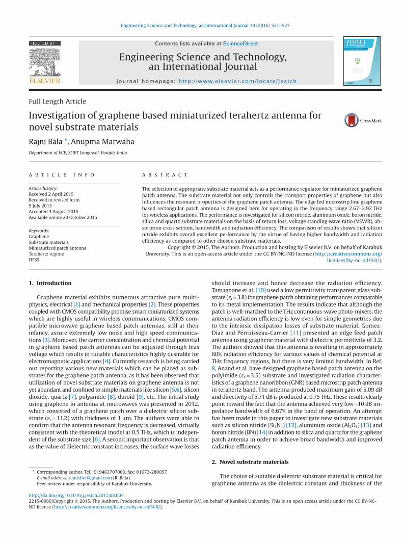
The rectangular patch antenna consisting of a conducting patchand a ground plane separated by a thin dielectric substrate is de-signed here as shown in Fig. 1. The rectangular patch printed ondifferent novel substrate materials is considered to be of same thick-ness “h”. In order to operate in the fundamental TM10 mode, thelength of the patch must be slightly less than λ/2, where λ is thewavelength in the dielectric medium and is equal to λo/√εreff, whereλo is the free space wavelength. The TM10 mode implies that the fieldvaries one λ/2 cycle along the length, and there is no variation alongthe width of the patch. Hence, an effective dielectric constant (εreff)must be obtained in order to account for the fringing and the wavepropagation in the line. The value of εreff is slightly less then εr becausethe fringing fields around the periphery of the patch are not con-fined in the dielectric substrate [20].The antenna is edge fed witha microstrip line with quarter wave transformer for providing theimpedance matching. The antenna is modeled and simulated usingFinite element method (FEM) based high frequency structure sim-ulator (HFSS) simulation software using different substrate materials
Fig. 1. Top view of graphene based rectangular patch antenna.
Table 1Properties of different substrate materials.
Substrate materials SI/metric Si3N4 Al2O3 BN Silica Quartz
Mechanical propertiesDensity gm/cc 3.29 3.69 1.9 2.2 2.5Elastic modulus GPa 310 300 46.9 – 60Poisson’s ratio – 0.27 0.21 – – –
Thermal propertiesThermal conductivity W/m·°K 30 18 30 1.5 1.4Coefficient of thermal expansion 10–6/°C 3.3 8.1 11.9 4.5 8Specific heat J/kg·°K 691 880 1610 745 750
Electrical propertiesDielectric constant – 9.5 9.1 4.6 4.0 3.78Dissipation factor – 0.0 0.0007 0.0017 – –
532 R. bala, A. marwaha/Engineering Science and Technology, an International Journal 19 (2016) 531–537

with properties as tabulated in Table 1. Table 2 details the designparameters of the graphene patch antenna.
HFSS utilizes differential equation based FEM full wave solverrequiring little analytical pre-processing. The 3D model of the
antenna is created for more realistic simulation. The computa-tional efficiency and accuracy is further enhanced due to the usefulfeature of automatic adaptive mesh generation and refinement. Thesimulations are executed subject to the suitable boundary condi-tions. The post-processing is further performed for analysis of resultsobtained by determination of other parameters based on the fielddistributions [21,22].
4. Performance evaluation
The use of graphene patch as conducting material for antennais expected to have enormous potential to enhance bandwidth andradiation efficiency due to extraordinary electromagnetic proper-ties and functionalities. The different antenna parameters such asgain, return loss, VSWR, absorption cross section and radiation char-acteristic have been determined for graphene patch antennafor appropriate selection of dielectric substrate to achieve the
Table 2Design specifications.
Design parameters Measurement
Length of patch (Lp) 22 μmWidth of patch (Wp) 30 μmHeight of substrate (h) 3 μmLength of substrate (Ls) 100 μmWidth of substrate (Ws) 63 μmLength of λ/4 transformer (L1) 14 μmWidth of λ/4 transformer (W1) 1.3 μmLength of feed (L2) 22 μmWidth of feed (W2) 5.5 μm
Fig. 2. Return loss (in dB) curves for different substrate materials, Si3N4 (red solid line), Al2O3 (green double dot line), silica (purple long dash line), quartz (brown doubledot dash line) and BN (blue solid line).
Fig. 3. VSWR curves for different substrate materials, Si3N4 (red solid line), Al2O3 (green double dot line), silica (purple long dash line), quartz (brown double dot dash line)and BN (blue solid line).
533R. bala, A. marwaha/Engineering Science and Technology, an International Journal 19 (2016) 531–537

enhanced performance parameters. The return loss should be lessthan −10 dB for proper impedance matching and is determined forthe model with various substrate materials as depicted in Fig. 2. Thesimulated result shows that the return loss values for respective res-onant mode frequencies is −26.71 dB for Si3N4 at 2.7 THz, −20.70 dBfor Al2O3 at 2.7 THz, −12.19 dB for BN at 2.9 THz, −21.23 dB for silicaat 2.81 THz and −16.02 dB for quartz at 2.87 THz. For the pro-posed design the impedance bandwidth achieved is in the rangeof 80–270 GHz at different resonant frequencies as depicted inTable 3. It can be clearly seen that the maximum bandwidth of270 GHz is obtained for the patch antenna on Si3N4 substrate.
VSWR values plotted in Fig. 3 depict the respective variationswell below 2. The Si3N4 substrate leads to VSWR value of nearly 1at the corresponding resonant frequency of 2.7 THz.
The present analysis has been performed on graphene model as-suming zero chemical potential thus limiting the achievable radiationefficiency. The radiation efficiency capabilities can however be com-pensated by using substrate material with higher dielectric constant.It is clearly evident from Fig. 4 that the radiation efficiency obtainedfor selected substrate materials is more than 87%, which is reason-ably good for design of graphene patch antenna for wireless applications.
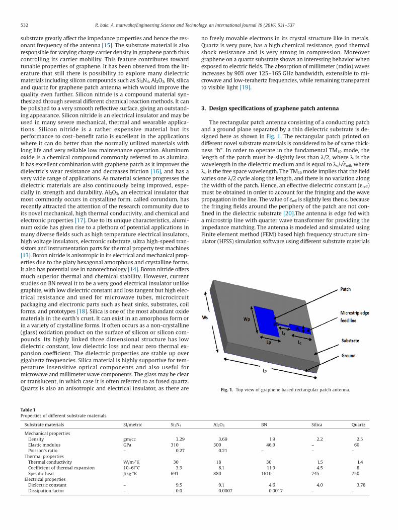
The antenna pattern describes the relative strength of the ra-diated field in multiple directions from the antenna. 2D and 3Dradiation patterns for different substrate materials of given antennaare shown in Figs. 5 and 6 respectively.
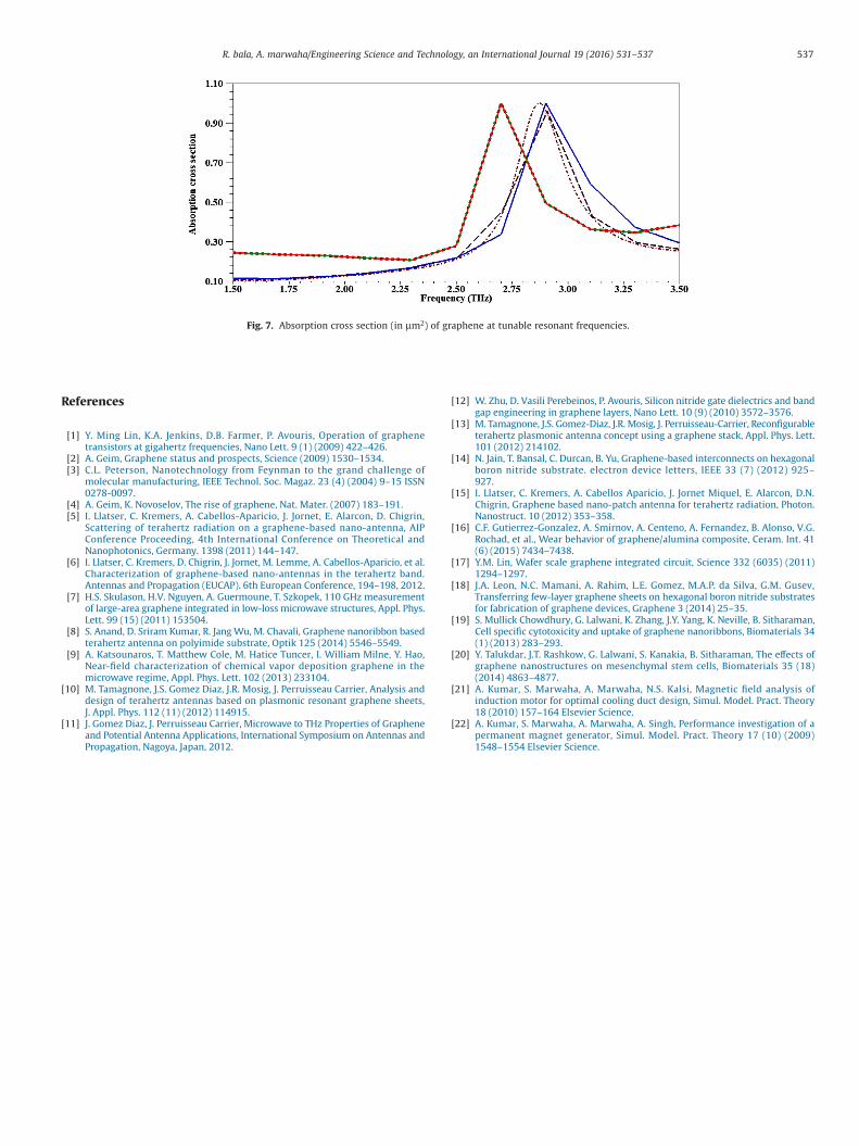
The absorption cross section is defined as the fractional inci-dent power absorbed by graphene and is expected to take maximumvalues at the resonant frequency [20]. Fig. 7 shows the absorptioncross section of graphene patch antenna for different substrate ma-terials acquired through numerical simulation.
The results obtained from the designed antenna for Si3N4, Al2O3,BN, quartz and silica as substrate materials depicted in Table 3 canbe used as a comparative measure for optimally selecting the sub-strate for the graphene patch antenna based on the evaluatedparameters.
5. Conclusions
In this paper, an attempt has been made to examine the effectof substrate material on the performance of microstrip edge feedantenna for terahertz regime. Quarter wave transformer is used foroptimizing the resonant properties. FEM based HFSS simulation soft-ware is used for numerical modeling of the designed antenna foroperating in the frequency range of 2.67–2.92 THz. In addition toconventional substrates novel materials have been suggested for ob-taining enhanced performance. Silicon nitride attains maximumreturn loss value of −26.71 dB with almost ideal value of VSWR. Itis observed that reasonably good dB gain with value more than 5 dBis achieved at the resonating frequency for all the substrate mate-rials. The −10 dB bandwidth for silicon nitride observed from thereturn loss plot is 270 GHz, which shows much improvement inbandwidth as compared with other substrate materials. Thereforeit can be concluded that silicon nitride can be the suitable choicefor substrate material for the graphene based miniaturized patchantenna for wireless applications.
Acknowledgements
This work is supported by the Department of Electronics andCommunication Engineering and the Department of Electrical andInstrumentation Engineering of Sant Longowal Institute of Engi-neering and Technology, Longowal, Punjab, by providing access toHigh Frequency Structural Simulator Software.
Table 3Performance comparison of miniaturized graphene patch antenna for various sub-strate materials.
Substrate parameters Resonatingfrequency(THz)
Returnl(dB)
VSWR Radiationefficiency(%)
−10 dBBandwidth(GHz)
Material Dielectricconstant
Si3N4 εr = 9.5 2.7 −26.71 1.1 100 270Al2O3 εr = 9.1 2.7 −20.70 1.2 98.4 240BN εr = 4.6 2.9 −12.19 1.7 87.9 80Silica εr = 4.0 2.81 −21.23 1.2 92.3 107.8Quartz εr = 3.78 2.87 −16.02 1.4 89.6 87.9
Fig. 4. Radiation efficiency curves for different substrate materials, Si3N4 (red solid line), Al2O3 (green double dot line), silica (purple long dash line), quartz (brown doubledot dash line) and BN (blue solid line).
534 R. bala, A. marwaha/Engineering Science and Technology, an International Journal 19 (2016) 531–537
Fig. 5. 2D Radiation patterns (a) Si3N4, (b) Al2O3, (c) BN, (d) silica and (e) quartz.
535R. bala, A. marwaha/Engineering Science and Technology, an International Journal 19 (2016) 531–537

Fig. 6. 3D Radiation patterns (a) Si3N4, (b) Al2O3, (c) BN, (d) silica and (e) quartz.
536 R. bala, A. marwaha/Engineering Science and Technology, an International Journal 19 (2016) 531–537
References
[1] Y. Ming Lin, K.A. Jenkins, D.B. Farmer, P. Avouris, Operation of graphenetransistors at gigahertz frequencies, Nano Lett. 9 (1) (2009) 422–426.
[2] A. Geim, Graphene status and prospects, Science (2009) 1530–1534.[3] C.L. Peterson, Nanotechnology from Feynman to the grand challenge of
molecular manufacturing, IEEE Technol. Soc. Magaz. 23 (4) (2004) 9–15 ISSN0278-0097.
[4] A. Geim, K. Novoselov, The rise of graphene, Nat. Mater. (2007) 183–191.[5] I. Llatser, C. Kremers, A. Cabellos-Aparicio, J. Jornet, E. Alarcon, D. Chigrin,
Scattering of terahertz radiation on a graphene-based nano-antenna, AIPConference Proceeding, 4th International Conference on Theoretical andNanophotonics, Germany. 1398 (2011) 144–147.
[6] I. Llatser, C. Kremers, D. Chigrin, J. Jornet, M. Lemme, A. Cabellos-Aparicio, et al.Characterization of graphene-based nano-antennas in the terahertz band.Antennas and Propagation (EUCAP). 6th European Conference, 194–198, 2012.
[7] H.S. Skulason, H.V. Nguyen, A. Guermoune, T. Szkopek, 110 GHz measurementof large-area graphene integrated in low-loss microwave structures, Appl. Phys.Lett. 99 (15) (2011) 153504.
[8] S. Anand, D. Sriram Kumar, R. Jang Wu, M. Chavali, Graphene nanoribbon basedterahertz antenna on polyimide substrate, Optik 125 (2014) 5546–5549.
[9] A. Katsounaros, T. Matthew Cole, M. Hatice Tuncer, I. William Milne, Y. Hao,Near-field characterization of chemical vapor deposition graphene in themicrowave regime, Appl. Phys. Lett. 102 (2013) 233104.
[10] M. Tamagnone, J.S. Gomez Diaz, J.R. Mosig, J. Perruisseau Carrier, Analysis anddesign of terahertz antennas based on plasmonic resonant graphene sheets,J. Appl. Phys. 112 (11) (2012) 114915.
[11] J. Gomez Diaz, J. Perruisseau Carrier, Microwave to THz Properties of Grapheneand Potential Antenna Applications, International Symposium on Antennas andPropagation, Nagoya, Japan, 2012.
[12] W. Zhu, D. Vasili Perebeinos, P. Avouris, Silicon nitride gate dielectrics and bandgap engineering in graphene layers, Nano Lett. 10 (9) (2010) 3572–3576.
[13] M. Tamagnone, J.S. Gomez-Diaz, J.R. Mosig, J. Perruisseau-Carrier, Reconfigurableterahertz plasmonic antenna concept using a graphene stack, Appl. Phys. Lett.101 (2012) 214102.
[14] N. Jain, T. Bansal, C. Durcan, B. Yu, Graphene-based interconnects on hexagonalboron nitride substrate. electron device letters, IEEE 33 (7) (2012) 925–927.
[15] I. Llatser, C. Kremers, A. Cabellos Aparicio, J. Jornet Miquel, E. Alarcon, D.N.Chigrin, Graphene based nano-patch antenna for terahertz radiation, Photon.Nanostruct. 10 (2012) 353–358.
[16] C.F. Gutierrez-Gonzalez, A. Smirnov, A. Centeno, A. Fernandez, B. Alonso, V.G.Rochad, et al., Wear behavior of graphene/alumina composite, Ceram. Int. 41(6) (2015) 7434–7438.
[17] Y.M. Lin, Wafer scale graphene integrated circuit, Science 332 (6035) (2011)1294–1297.
[18] J.A. Leon, N.C. Mamani, A. Rahim, L.E. Gomez, M.A.P. da Silva, G.M. Gusev,Transferring few-layer graphene sheets on hexagonal boron nitride substratesfor fabrication of graphene devices, Graphene 3 (2014) 25–35.
[19] S. Mullick Chowdhury, G. Lalwani, K. Zhang, J.Y. Yang, K. Neville, B. Sitharaman,Cell specific cytotoxicity and uptake of graphene nanoribbons, Biomaterials 34(1) (2013) 283–293.
[20] Y. Talukdar, J.T. Rashkow, G. Lalwani, S. Kanakia, B. Sitharaman, The effects ofgraphene nanostructures on mesenchymal stem cells, Biomaterials 35 (18)(2014) 4863–4877.
[21] A. Kumar, S. Marwaha, A. Marwaha, N.S. Kalsi, Magnetic field analysis ofinduction motor for optimal cooling duct design, Simul. Model. Pract. Theory18 (2010) 157–164 Elsevier Science.
[22] A. Kumar, S. Marwaha, A. Marwaha, A. Singh, Performance investigation of apermanent magnet generator, Simul. Model. Pract. Theory 17 (10) (2009)1548–1554 Elsevier Science.
Fig. 7. Absorption cross section (in μm2) of graphene at tunable resonant frequencies.
537R. bala, A. marwaha/Engineering Science and Technology, an International Journal 19 (2016) 531–537