investigation of asymmetric effects due to gate misalignment, gate bias and underlap length in...
TRANSCRIPT
Physica E 46 (2012) 61–67
Contents lists available at SciVerse ScienceDirect
Physica E
1386-94
http://d
n Corr
E-m
journal homepage: www.elsevier.com/locate/physe
Investigation of asymmetric effects due to gate misalignment, gate biasand underlap length in III–V heterostructure underlap DG MOSFET
Hemant Pardeshi a,n, Sudhansu Kumar Pati a, Godwin Raj a, N Mohankumar b, Chandan Kumar Sarkar a
a Electronics and Telecommunication Engineering Department, Jadavpur University, Kolkata, Indiab SKP Engineering College, Tiruvannamalai, Tamilnadu, India
H I G H L I G H T S
c Device uses narrowband In0.53Ga0.47As and wideband InP layers for body.c BG_D provide lower DIBL, Ioff, Delay & BG_S provide lower SS, higher Ion, Ion/Ioff.c Varying drain underlap reduces DIBL, SS, Delay, Ioff and increase Vt, Ion/Ioff.c 4T configuration provide excellent Vt, subthreshold leakage, delay control.c 4T reduces energy delay product and provides higher Ion/Ioff.
a r t i c l e i n f o
Article history:
Received 11 August 2012
Accepted 1 September 2012Available online 19 September 2012
77/$ - see front matter & 2012 Elsevier B.V. A
x.doi.org/10.1016/j.physe.2012.09.011
esponding author. Tel.: þ91 8296430311.
ail address: [email protected] (H. Parde
a b s t r a c t
In the present work, we investigate the influence of asymmetry in III–V heterostructure underlap DG
MOSFET caused by back gate movement, back gate voltages and drain side underlap length. The device
has narrowband In0.53Ga0.47As and wideband InP layers in the channel, along with high-K Al2O3 as the
gate dielectric. The 2D Sentaurus TCAD simulations are done using drift diffusion model and interface
traps are considered. The simulation model is calibrated with the previous reported experimental
results. For the same gate misalignment value, back gate shift toward drain (BG_D) resulted in a lower
DIBL, Ioff and Delay, than back gate shift towards source (BG_S). Conversely, BG_S results in lower SS,
higher Ion and Ion/Ioff ratio. Excellent threshold voltage controllability, reduced delay, reduced energy
delay product, higher Ion/Ioff ratio are achieved by varying back gate voltage. Varying drain underlap
reduces DIBL, SS, Delay, Ioff and increases Vt and Ion/Ioff ratio. Thus, application specific optimized device
parameters can be achieved with asymmetrical device structure, asymmetrical gate bias or its
combination.
& 2012 Elsevier B.V. All rights reserved.
1. Introduction
The underlap DG MOSFET is a promising candidate to extendthe CMOS scaling roadmap, with reduced short channel effects[1,2]. Underlap structure reduces the overall and fringe capaci-tance, thereby increasing the switching speed and reducing thedelay [3]. Underlap DG MOSFET should have an ultrathin body,aligned source/drain and aligned front and back gates, to possessideal device characteristics. However, during the fabrication ofsub 100 nm regime devices, prefect alignment is very difficultto achieve [4]. Thus, it is necessary to study the tolerance rangefor gate misalignment causing asymmetry and its impact onthe device performance characteristics. Furthermore, threshold
ll rights reserved.
shi).
voltage (Vt) can also be controlled by varying the back gatevoltage thus, making the device more versatile for both highspeed and low power dissipation applications [5]. Substantialreduction in the subthreshold leakage current by increasing thedrain side underlap length is reported [6]. The impact of symme-trical underlap length on the device on current (Ion) and OFFcurrent (Ioff) was reported for silicon underlap DG MOSFET byKanti [7].
For short channel devices operating in the subthresholdregion, the subthreshold leakage current dominates the draincurrent. Subthreshold leakage occurs when the transistor is off,due to the diffusion of carriers from source to drain [8]. Therefore,as the channel length decreases with scaling, the Ioff currentincreases, due to Vt roll-off which, eventually causes an increasein stand-by power. On the other hand, there is demand to reduceVt in order to improve Ion, but lower Vt leads to increasedsubthreshold leakage. Vt controllability is thus a major issue in
H. Pardeshi et al. / Physica E 46 (2012) 61–6762
CMOS applications. Analysis of asymmetric effect can be helpfulto optimize device parameters like Vt, Ion, Ioff, Delay and shortchannel effect, for specific application.
In our previous work, we have proposed novel III–V materialbased heterostucture underlap MOSFET and compared with thesilicon underlap device. The III–V heterostructure device showedexcellent control of SCE, reduced delay and higher Ion current thansilicon underlap for same device dimensions. In this paper, weperform Sentaurus TCAD simulator to study the asymmetricbehaviour of the heterostructure underlap DG MOSFET. Asym-metric behaviour is analysed by moving the back towards sourceor drain ends, thus inducing gate misalignment. As the gate ismisaligned the underlap length increases on one side anddecreases on other side. For example, as the gate terminal movestowards the source end, the underlap length in the source side(Lus) decreases and the underlap length in the drain side (Lud)increases, and vice versa. Second, underlap DG MOSFETs can beconfigured to have either a three-terminal (3T) tied gate or a four-terminal (4T) independent gate configuration. In 3T configuration,both the gates are connected to each other and have commonapplied voltage. In 4T configuration the back gate bias is keptfixed and the front gate acts as the control electrode, independentof back gate bias. In the underlap DG MOS structure, applicationof different gate voltages at the front and back gate can introduceasymmetry. Asymmetry can also be induced by changing eithersource or drain side underlap length while maintaining the otherside underlap length constant. For example, Lus is constant and Lud
is varied. Alternatively, asymmetry can be by virtue of differentgate oxide thickness for front and back gate, and by different workfunction gates.
2. Device description
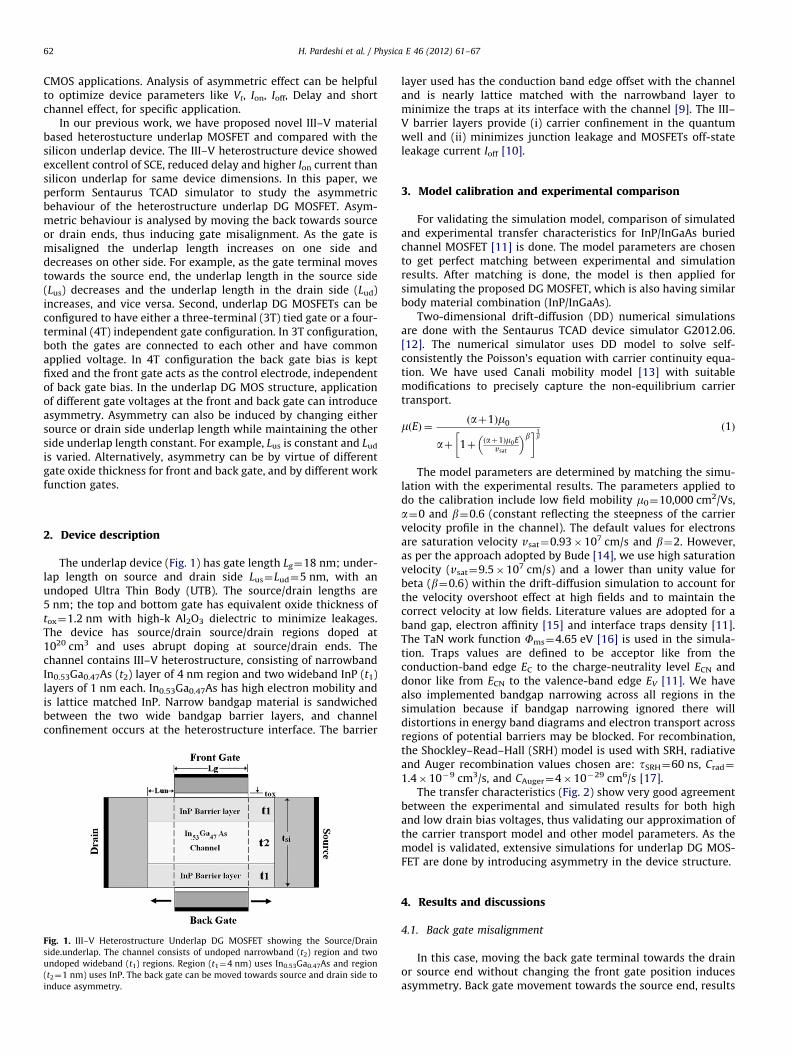
The underlap device (Fig. 1) has gate length Lg¼18 nm; under-lap length on source and drain side Lus¼Lud¼5 nm, with anundoped Ultra Thin Body (UTB). The source/drain lengths are5 nm; the top and bottom gate has equivalent oxide thickness oftox¼1.2 nm with high-k Al2O3 dielectric to minimize leakages.The device has source/drain source/drain regions doped at1020 cm3 and uses abrupt doping at source/drain ends. Thechannel contains III–V heterostructure, consisting of narrowbandIn0.53Ga0.47As (t2) layer of 4 nm region and two wideband InP (t1)layers of 1 nm each. In0.53Ga0.47As has high electron mobility andis lattice matched InP. Narrow bandgap material is sandwichedbetween the two wide bandgap barrier layers, and channelconfinement occurs at the heterostructure interface. The barrier
Fig. 1. III–V Heterostructure Underlap DG MOSFET showing the Source/Drain
side.underlap. The channel consists of undoped narrowband (t2) region and two
undoped wideband (t1) regions. Region (t1¼4 nm) uses In0.53Ga0.47As and region
(t2¼1 nm) uses InP. The back gate can be moved towards source and drain side to
induce asymmetry.
layer used has the conduction band edge offset with the channeland is nearly lattice matched with the narrowband layer tominimize the traps at its interface with the channel [9]. The III–V barrier layers provide (i) carrier confinement in the quantumwell and (ii) minimizes junction leakage and MOSFETs off-stateleakage current Ioff [10].
3. Model calibration and experimental comparison
For validating the simulation model, comparison of simulatedand experimental transfer characteristics for InP/InGaAs buriedchannel MOSFET [11] is done. The model parameters are chosento get perfect matching between experimental and simulationresults. After matching is done, the model is then applied forsimulating the proposed DG MOSFET, which is also having similarbody material combination (InP/InGaAs).
Two-dimensional drift-diffusion (DD) numerical simulationsare done with the Sentaurus TCAD device simulator G2012.06.[12]. The numerical simulator uses DD model to solve self-consistently the Poisson’s equation with carrier continuity equa-tion. We have used Canali mobility model [13] with suitablemodifications to precisely capture the non-equilibrium carriertransport.
mðEÞ ¼ ðaþ1Þm0
aþ 1þ ðaþ1Þm0Evsat
� �b� �1b
ð1Þ
The model parameters are determined by matching the simu-lation with the experimental results. The parameters applied todo the calibration include low field mobility m0¼10,000 cm2/Vs,a¼0 and b¼0.6 (constant reflecting the steepness of the carriervelocity profile in the channel). The default values for electronsare saturation velocity vsat¼0.93�107 cm/s and b¼2. However,as per the approach adopted by Bude [14], we use high saturationvelocity (vsat¼9.5�107 cm/s) and a lower than unity value forbeta (b¼0.6) within the drift-diffusion simulation to account forthe velocity overshoot effect at high fields and to maintain thecorrect velocity at low fields. Literature values are adopted for aband gap, electron affinity [15] and interface traps density [11].The TaN work function Fms¼4.65 eV [16] is used in the simula-tion. Traps values are defined to be acceptor like from theconduction-band edge EC to the charge-neutrality level ECN anddonor like from ECN to the valence-band edge EV [11]. We havealso implemented bandgap narrowing across all regions in thesimulation because if bandgap narrowing ignored there willdistortions in energy band diagrams and electron transport acrossregions of potential barriers may be blocked. For recombination,the Shockley–Read–Hall (SRH) model is used with SRH, radiativeand Auger recombination values chosen are: tSRH¼60 ns, Crad¼
1.4�10�9 cm3/s, and CAuger¼4�10�29 cm6/s [17].The transfer characteristics (Fig. 2) show very good agreement
between the experimental and simulated results for both highand low drain bias voltages, thus validating our approximation ofthe carrier transport model and other model parameters. As themodel is validated, extensive simulations for underlap DG MOS-FET are done by introducing asymmetry in the device structure.
4. Results and discussions
4.1. Back gate misalignment
In this case, moving the back gate terminal towards the drainor source end without changing the front gate position inducesasymmetry. Back gate movement towards the source end, results
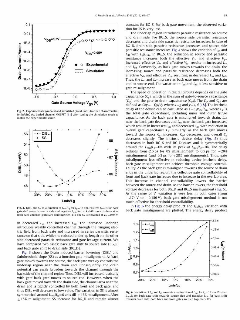
Fig. 2. Experimental (symbols) and simulated (solid lines) transfer characteristics
for.InP/InGaAs buried channel MOSFET [11] after tuning the simulation mode to
match the experimental curve.
Fig. 3. DIBL and SS as a function of Lmis/Lg for Lg¼18 nm. Positive Lmis is for back
gate.shift towards source side and negative Lmis for back shift towards drain side.
Both back and front gates are tied together (3T). The SS is extracted at Vds¼0.05 V.
Fig. 4. Variation of Ion and Ioff currents as a function of Lmis for Lg¼18 nm. Positive
Lmis.is for back gate shift towards source side and negative Lmis for back shift
towards drain side. Both back and front gates are tied together (3T).
H. Pardeshi et al. / Physica E 46 (2012) 61–67 63
in decreased Lus and increased Lud. The increased underlapintroduces weakly controlled channel through the fringing elec-tric field from back gate and increased in series parasitic resis-tance on that side, while the reduced underlap length on the otherside decreased parasitic resistance and gate leakage current. Wehave compared two cases: back gate shift to source side (BG_S)and back gate shift to drain side (BG_D).
Fig. 3 shows the Drain induced barrier lowering (DIBL) andSubthreshold slope (SS) as a function gate misalignment. As backgate moves towards the source, the back gate weakly controls theunderlap region near the drain end. Consequently, the drainpotential can easily broaden towards the channel through thebackside of the channel region. Thus, DIBL will increase drasticallywith gate back gate moves to source end. However, when theback gate moved towards the drain side, the channel area near thedrain end is tightly controlled by both front and back gate, andthus DIBL will decrease to low value. The variation in SS is almostsymmetrical around Lmis/Lg¼0 axis till 715% misalignment. After715% misalignment, SS increase for BG_D and remain almost
constant for BG_S. For back gate movement, the observed varia-tion for SS is very less.
The underlap region introduces parasitic resistance on sourceand drain side. For BG_S, the source side parasitic resistancedecreases and drain side parasitic resistance increases. In case ofBG_D, drain side parasitic resistance decreases and source sideparasitic resistance increases. Fig. 4 shows the variation of Ion andIoff with Lg/Lmis. In BG_S, the reduction in source end parasiticresistance increases both the effective Vds and effective Vgs.Increased effective Vds and effective Vgs, results in increased Ion
and Ioff. Conversely, as back gate moves towards the drain, theincreasing source end parasitic resistance decreases both theeffective Vds and effective Vgs, resulting in decreased Ion and Ioff.Thus, the Ion and Ioff increase as back gate moves from the drainend to source end. The variation in Ion and Ioff is less sensitive togate misalignment.
The speed of operation in digital circuits depends on the gatecapacitance (Cg), which is the sum of gate-to-source capacitance(Cgs) and the gate-to-drain capacitance (Cgd). The Cgs and Cgd aredefined as Cxy¼�Qx/Vy where x¼g and y¼s, d [18]. The Intrinsicdelay of the device can be calculated as t¼CgVDD/Ion, where Cg isthe total gate capacitance, including inner and outer fringecapacitance. As the back gate is misaligned towards drain, Lud
near the back gate decreases and Lus near the back gate increases,which results in increased Cgd and decreased Cgs, with reduction inoverall gate capacitance Cg. Similarly, as the back gate movestoward the source Cgs increases, Cgd decreases, and overall Cg
decreases slightly. The intrinsic device delay (Fig. 5) thusdecreases in both BG_S and BG_D cases and is symmetricallyaround the Lmis/Lg¼0% with its peak at Lmis/Lg¼0%. The delayreduces from 2.6 ps for 0% misalignment to 0.5 ps for �28%misalignment (and 0.3 ps forþ28% misalignments). Thus, gatemisalignment less effective in reducing device intrinsic delay.Back gate misalignment can achieve threshold voltage controll-ability. As the back gate is misaligned towards the source or drainends in the underlap region, the collective gate controllability offront and back gate increases due to increase in the overlap area.This increase in channel controllability lowers the barrierbetween the source and drain. As the barrier lowers, the thresholdvoltage decreases for both BG_D and BG_S misalignment (Fig. 5).As the range of Vt variation is very less in both cases (from� .174 V to �0.156 V), back gate misalignment method is notmuch effective for threshold controllability.
In Fig. 6 the energy delay product and Ion/Ioff variation withback gate misalignment are plotted. The energy delay product
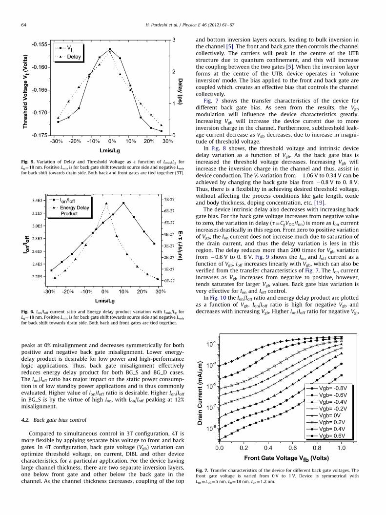
Fig. 5. Variation of Delay and Threshold Voltage as a function of Lmis/Lg for
Lg¼18 nm. Positive Lmis is for back gate shift towards source side and negative Lmis
for back shift towards drain side. Both back and front gates are tied together (3T).
Fig. 6. Ion/Ioff current ratio and Energy delay product variation with Lmis/Lg for
Lg¼18 nm. Positive Lmis is for back gate shift towards source side and negative Lmis
for back shift towards drain side. Both back and front gates are tied together.
Fig. 7. Transfer characteristics of the device for different back gate voltages. The
front gate voltage is varied from 0 V to 1 V. Device is symmetrical with
Lus¼Lud¼5 nm, Lg¼18 nm, tox¼1.2 nm.
H. Pardeshi et al. / Physica E 46 (2012) 61–6764
peaks at 0% misalignment and decreases symmetrically for bothpositive and negative back gate misalignment. Lower energy-delay product is desirable for low power and high-performancelogic applications. Thus, back gate misalignment effectivelyreduces energy delay product for both BG_S and BG_D cases.The Ion/Ioff ratio has major impact on the static power consump-tion is of low standby power applications and is thus commonlyevaluated. Higher value of Ion/Ioff ratio is desirable. Higher Ion/Ioff
in BG_S is by the virtue of high Ion, with Ion/Ioff peaking at 12%misalignment.
4.2. Back gate bias control
Compared to simultaneous control in 3T configuration, 4T ismore flexible by applying separate bias voltage to front and backgates. In 4T configuration, back gate voltage (Vgb) variation canoptimize threshold voltage, on current, DIBL and other devicecharacteristics, for a particular application. For the device havinglarge channel thickness, there are two separate inversion layers,one below front gate and other below the back gate in thechannel. As the channel thickness decreases, coupling of the top
and bottom inversion layers occurs, leading to bulk inversion inthe channel [5]. The front and back gate then controls the channelcollectively. The carriers will peak in the centre of the UTBstructure due to quantum confinement, and this will increasethe coupling between the two gates [5]. When the inversion layerforms at the centre of the UTB, device operates in ‘volumeinversion’ mode. The bias applied to the front and back gate arecoupled which, creates an effective bias that controls the channelcollectively.
Fig. 7 shows the transfer characteristics of the device fordifferent back gate bias. As seen from the results, the Vgb
modulation will influence the device characteristics greatly.Increasing Vgb will increase the device current due to moreinversion charge in the channel. Furthermore, subthreshold leak-age current decrease as Vgb decreases, due to increase in magni-tude of threshold voltage.
In Fig. 8 shows, the threshold voltage and intrinsic devicedelay variation as a function of Vgb. As the back gate bias isincreased the threshold voltage decreases. Increasing Vgb willincrease the inversion charge in the channel and thus, assist indevice conduction. The Vt variation from �1.06 V to 0.34 V can beachieved by changing the back gate bias from �0.8 V to 0. 8 V.Thus, there is a flexibility in achieving desired threshold voltage,without affecting the process conditions like gate length, oxideand body thickness, doping concentration, etc. [19].
The device intrinsic delay also decreases with increasing backgate bias. For the back gate voltage increases from negative valueto zero, the variation in delay (t¼CgVDD/Ion) is more as Ion currentincreases drastically in this region. From zero to positive variationof Vgb, the Ion current does not increase much due to saturation ofthe drain current, and thus the delay variation is less in thisregion. The delay reduces more than 200 times for Vgb variationfrom �0.6 V to 0. 8 V. Fig. 9 shows the Ion and Ioff current as afunction of Vgb. Ioff increases linearly with Vgb, which can also beverified from the transfer characteristics of Fig. 7. The Ion currentincreases as Vgb increases from negative to positive, however,tends saturates for larger Vgb values. Back gate bias variation isvery effective for Ion and Ioff control.
In Fig. 10 the Ion/Ioff ratio and energy delay product are plottedas a function of Vgb. Ion/Ioff ratio is high for negative Vgb anddecreases with increasing Vgb. Higher Ion/Ioff ratio for negative Vgb
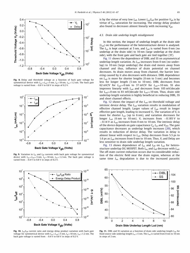
Fig. 8. Delay and threshold voltage as a function of back gate voltage for
symmetrical device with Lus¼Lud¼5 nm, Lg¼18 nm, tox¼1.2 nm. The back gate
voltage is varied from �0.8 V to 0.8 V in steps of 0.2 V.
Fig. 9. Variation in Ion and Ioff currents with back gate voltage for symmetrical
device with Lus¼Lud¼5 nm, Lg¼18 nm, tox¼1.2 nm. The back gate voltage is
varied from �0.4 V to 0.8 V in steps of 0.2 V.
Fig. 10. Ion/Ioff current ratio and energy delay product variation with back gate
voltage for symmetrical device with Lus¼Lud¼5 nm, Lg¼18 nm, tox¼1.2 nm. The
back gate voltage is varied from �0.4 V to 0.8 V in steps of 0.2 V.
H. Pardeshi et al. / Physica E 46 (2012) 61–67 65
is by the virtue of very low Ioff. Lower Ion/Ioff for positive Vgb is byvirtue of Ion saturation for increasing. The energy delay productalso found to decreases almost linearly with increasing Vgb.
4.3. Drain side underlap length misalignment
In this section, the impact of underlap length at the drain side(Lud) on the performance of the heterostructure device is analysed.The Lus is kept constant at 5 nm, and Lud is varied from 0 nm (nounderlap at the drain side) to 10 nm (large underlap at the drainside), with the front gate and back gate are tied together (3T).
Fig. 11 shows the dependence of DIBL and SS on asymmetricalunderlap length variation. As Lud increases from 0 nm (no under-lap) to 10 nm (large underlap) the drain end moves away fromchannel and thus, influence of drain potential on channeldecreases. As drain moves away from channel, the barrier low-ering caused by it also decreases with distance. DIBL dependenceon Lud is more for shorter lengths (0 nm to 5 nm) and becomesless for longer length (5 nm to 10 nm). DIBL decreases from62 mV/V for Lud¼0 nm to 37 mV/V for Lud¼10 nm. SS alsoimproves linearly with Lud and decreases from 105 mV/decadefor Lud¼0 nm to 81 mV/decade for Lud¼10 nm. Thus, drain sideunderlap length variation is highly beneficial in reducing DIBL, SSand short channel effects.
Fig. 12 shows the impact of the Lud on threshold voltage andintrinsic device delay. The Lud variation results in modulation ofeffective channel length. Larger values of Lud result in longereffective gate length, leading to increased Vt. The variation of Vt ismore for shorter Lud (up to 6 nm), and variation decreases forlonger Lud (6 nm to 10 nm). Vt increases from �0.185 V to�0.14 V as Lud increases from 0 nm to 10 nm. The intrinsic delayof the device depends on gate capacitance Cg, Ion and VDD. The gatecapacitance decreases as underlap length increases [20], whichresults in reduction of device delay. The variation in delay isalmost linear with respect to Lud. Delay decreases from 5.5 ps to1.6 ps as Lud increases from 0 nm to 10 nm. Thus, Vt and Delay areless sensitive to drain side underlap length variation.
Fig. 13 shows dependence of Ion and Ioff on Lud for hetero-stucture underlap DG MOSFET. Both Ion and Ioff decrease with Lud.The off-state current reduction occurs due to considerable reduc-tion of the electric field near the drain region, whereas at thesame time Ion degradation is due to the increased parasitic
Fig. 11. DIBL and SS variation as a function of drain side underlap length Lud for
fixed source side underlap length Lus¼5 nm. The Lud is varied from 0 nm to 10 nm
in steps of 2 nm.
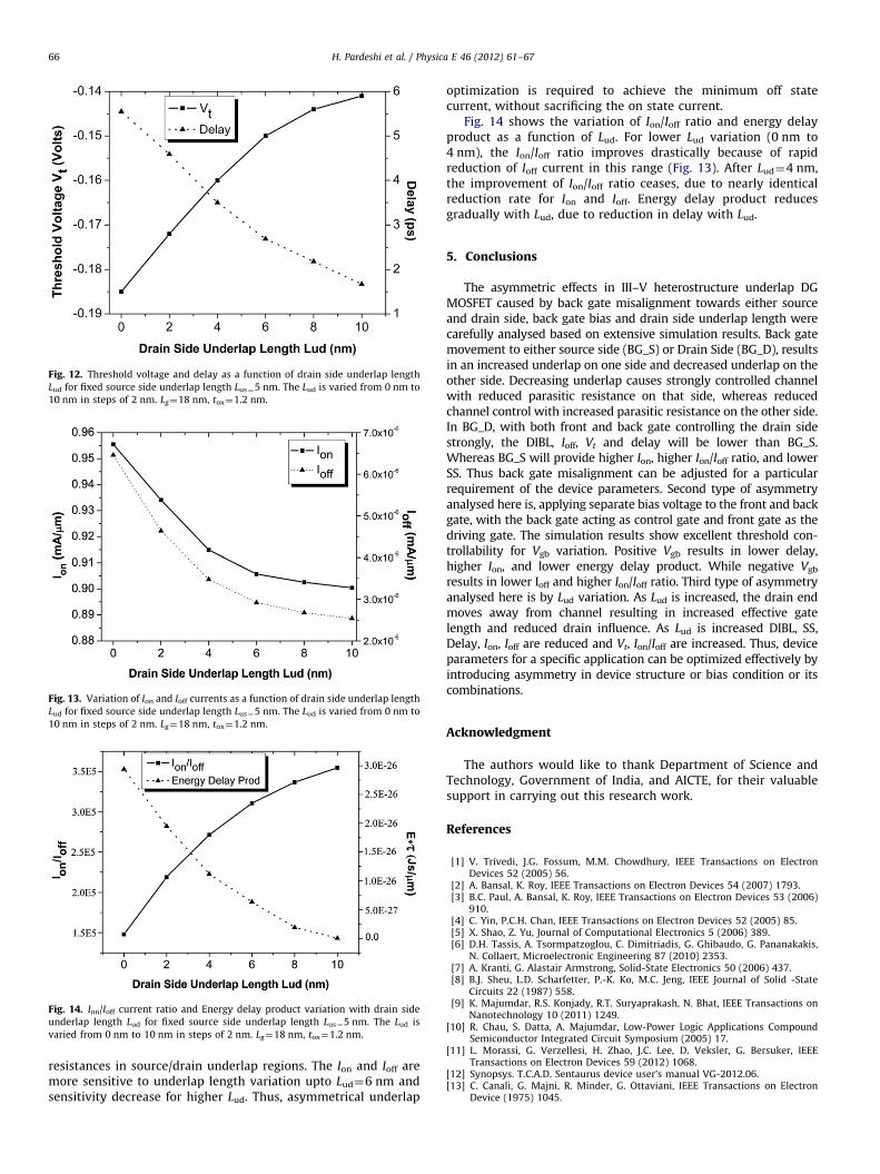
Fig. 12. Threshold voltage and delay as a function of drain side underlap length
Lud for fixed source side underlap length Lus¼5 nm. The Lud is varied from 0 nm to
10 nm in steps of 2 nm. Lg¼18 nm, tox¼1.2 nm.
Fig. 13. Variation of Ion and Ioff currents as a function of drain side underlap length
Lud for fixed source side underlap length Lus¼5 nm. The Lud is varied from 0 nm to
10 nm in steps of 2 nm. Lg¼18 nm, tox¼1.2 nm.
Fig. 14. Ion/Ioff current ratio and Energy delay product variation with drain side
underlap length Lud for fixed source side underlap length Lus¼5 nm. The Lud is
varied from 0 nm to 10 nm in steps of 2 nm. Lg¼18 nm, tox¼1.2 nm.
H. Pardeshi et al. / Physica E 46 (2012) 61–6766
resistances in source/drain underlap regions. The Ion and Ioff aremore sensitive to underlap length variation upto Lud¼6 nm andsensitivity decrease for higher Lud. Thus, asymmetrical underlap
optimization is required to achieve the minimum off statecurrent, without sacrificing the on state current.
Fig. 14 shows the variation of Ion/Ioff ratio and energy delayproduct as a function of Lud. For lower Lud variation (0 nm to4 nm), the Ion/Ioff ratio improves drastically because of rapidreduction of Ioff current in this range (Fig. 13). After Lud¼4 nm,the improvement of Ion/Ioff ratio ceases, due to nearly identicalreduction rate for Ion and Ioff. Energy delay product reducesgradually with Lud, due to reduction in delay with Lud.
5. Conclusions
The asymmetric effects in III–V heterostructure underlap DGMOSFET caused by back gate misalignment towards either sourceand drain side, back gate bias and drain side underlap length werecarefully analysed based on extensive simulation results. Back gatemovement to either source side (BG_S) or Drain Side (BG_D), resultsin an increased underlap on one side and decreased underlap on theother side. Decreasing underlap causes strongly controlled channelwith reduced parasitic resistance on that side, whereas reducedchannel control with increased parasitic resistance on the other side.In BG_D, with both front and back gate controlling the drain sidestrongly, the DIBL, Ioff, Vt and delay will be lower than BG_S.Whereas BG_S will provide higher Ion, higher Ion/Ioff ratio, and lowerSS. Thus back gate misalignment can be adjusted for a particularrequirement of the device parameters. Second type of asymmetryanalysed here is, applying separate bias voltage to the front and backgate, with the back gate acting as control gate and front gate as thedriving gate. The simulation results show excellent threshold con-trollability for Vgb variation. Positive Vgb results in lower delay,higher Ion, and lower energy delay product. While negative Vgb
results in lower Ioff and higher Ion/Ioff ratio. Third type of asymmetryanalysed here is by Lud variation. As Lud is increased, the drain endmoves away from channel resulting in increased effective gatelength and reduced drain influence. As Lud is increased DIBL, SS,Delay, Ion, Ioff are reduced and Vt, Ion/Ioff are increased. Thus, deviceparameters for a specific application can be optimized effectively byintroducing asymmetry in device structure or bias condition or itscombinations.
Acknowledgment
The authors would like to thank Department of Science andTechnology, Government of India, and AICTE, for their valuablesupport in carrying out this research work.
References
[1] V. Trivedi, J.G. Fossum, M.M. Chowdhury, IEEE Transactions on ElectronDevices 52 (2005) 56.
[2] A. Bansal, K. Roy, IEEE Transactions on Electron Devices 54 (2007) 1793.[3] B.C. Paul, A. Bansal, K. Roy, IEEE Transactions on Electron Devices 53 (2006)
910.[4] C. Yin, P.C.H. Chan, IEEE Transactions on Electron Devices 52 (2005) 85.[5] X. Shao, Z. Yu, Journal of Computational Electronics 5 (2006) 389.[6] D.H. Tassis, A. Tsormpatzoglou, C. Dimitriadis, G. Ghibaudo, G. Pananakakis,
N. Collaert, Microelectronic Engineering 87 (2010) 2353.[7] A. Kranti, G. Alastair Armstrong, Solid-State Electronics 50 (2006) 437.[8] B.J. Sheu, L.D. Scharfetter, P.-K. Ko, M.C. Jeng, IEEE Journal of Solid -State
Circuits 22 (1987) 558.[9] K. Majumdar, R.S. Konjady, R.T. Suryaprakash, N. Bhat, IEEE Transactions on
Nanotechnology 10 (2011) 1249.[10] R. Chau, S. Datta, A. Majumdar, Low-Power Logic Applications Compound
Semiconductor Integrated Circuit Symposium (2005) 17.[11] L. Morassi, G. Verzellesi, H. Zhao, J.C. Lee, D. Veksler, G. Bersuker, IEEE
Transactions on Electron Devices 59 (2012) 1068.[12] Synopsys. T.C.A.D. Sentaurus device user’s manual VG-2012.06.[13] C. Canali, G. Majni, R. Minder, G. Ottaviani, IEEE Transactions on Electron
Device (1975) 1045.
H. Pardeshi et al. / Physica E 46 (2012) 61–67 67
[14] J.D. Bude, Simulation of Semiconductor Processes and Devices SISPAD 2000,(2000) 23.
[15] Ioffe Institute, New Semiconductor Materials. Characteristics and Properties.[Online]. Available: /http://www.ioffe.ru/SVA/NSM/S.
[16] K. Choi, H.N. Alshareef, H.C. Wen, H. Harris, H. Luan, Y. Senzaki, P. Lysaght,P. Majhi, B.H. Lee, Applied Physics Express 89 (2006) 87.
[17] G. Ji, H.-G. Liu, Y.-B. Su, Y.-X. Cao, Z. Jin, Chinese Physics B 21 (2012) 058501-1to 058501-6.
[18] G.C. Patil, S. Qureshi, IEEE Computer Society Annual Symposium on VLSI 2011(2011) 43.
[19] R. Vaddi, S. Dasgupta, R.P. Agarwal, IEEE Computer Society Annual Sympo-
sium on VLSI 2011 (2011) 37.[20] A. Bansal, B.C. Paul, K. Roy, IEEE Transactions on Electron Devices 52 (2005)
256.