introduction to verilog design - university of california...
TRANSCRIPT
1
ECE 156A 1
Introduction to Verilog design
Lecture 2
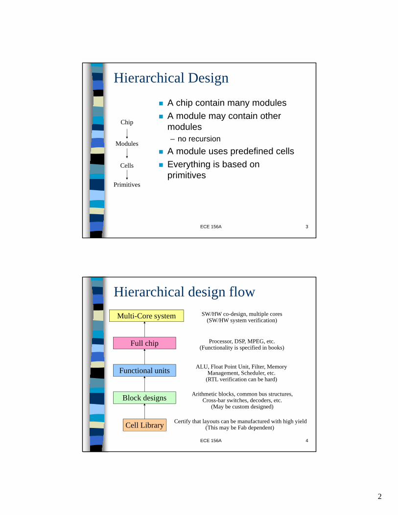
Design flow (from the book)
ECE 156A 2
2
ECE 156A 3
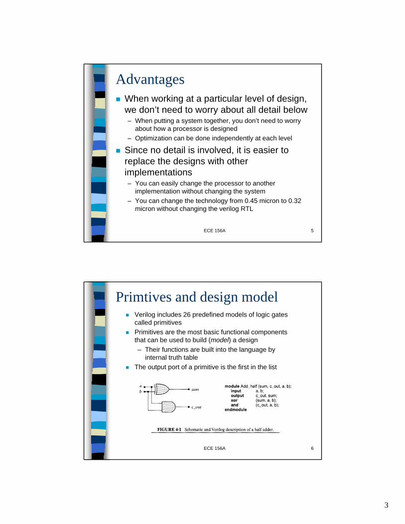
Hierarchical DesignA chip contain many modulesA module may contain other modules– no recursion
A module uses predefined cellsEverything is based on primitives
Chip
Modules
Cells
Primitives
ECE 156A 4
Hierarchical design flow
Cell Library
Block designs
Functional units
Full chip
Multi-Core system
Certify that layouts can be manufactured with high yield(This may be Fab dependent)
Arithmetic blocks, common bus structures,Cross-bar switches, decoders, etc.
(May be custom designed)
ALU, Float Point Unit, Filter, MemoryManagement, Scheduler, etc.
(RTL verification can be hard)
Processor, DSP, MPEG, etc.(Functionality is specified in books)
SW/HW co-design, multiple cores(SW/HW system verification)
3
ECE 156A 5
AdvantagesWhen working at a particular level of design, we don’t need to worry about all detail below– When putting a system together, you don’t need to worry
about how a processor is designed– Optimization can be done independently at each level
Since no detail is involved, it is easier to replace the designs with other implementations– You can easily change the processor to another
implementation without changing the system– You can change the technology from 0.45 micron to 0.32
micron without changing the verilog RTL
Primtives and design model
ECE 156A 6
Verilog includes 26 predefined models of logic gates called primitivesPrimitives are the most basic functional components that can be used to build (model) a design– Their functions are built into the language by
internal truth tableThe output port of a primitive is the first in the list
4
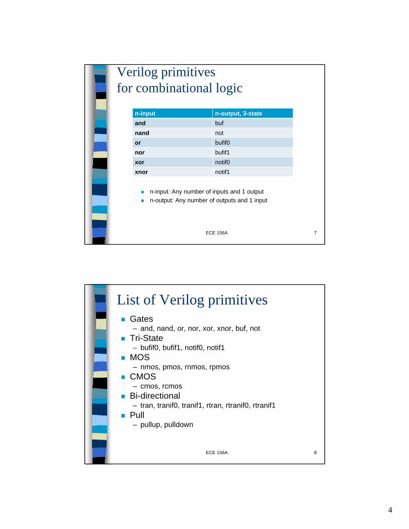
Verilog primitives for combinational logic
ECE 156A 7
n-input n-output, 3-stateand bufnand notor bufif0nor bufif1xor notif0xnor notif1
n-input: Any number of inputs and 1 outputn-output: Any number of outputs and 1 input
ECE 156A 8
List of Verilog primitivesGates– and, nand, or, nor, xor, xnor, buf, not
Tri-State– bufif0, bufif1, notif0, notif1
MOS– nmos, pmos, rnmos, rpmos
CMOS– cmos, rcmos
Bi-directional– tran, tranif0, tranif1, rtran, rtranif0, rtranif1
Pull– pullup, pulldown
5
Standard cells vs. PrimitivesVerilog primitives are abstract building blocks used to model your design– They are not real
Standard cells are real building blocks used to implement your design– Each has a corresponding layout– Each has a timing model– Cells are stored in a cell library– Cell library is NOT free; you need to buy
ECE 156A 9
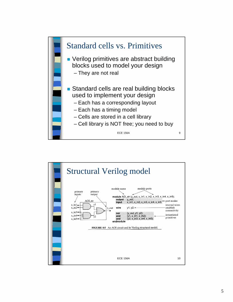
Structural Verilog model
ECE 156A 10

6
ECE 156A 11
Verilog Behavior of D FFmodule Flip_flop (q, data_in,
clk, rst);input data_in, clk, rst;output q;reg q;
always @ (posedge clk)beginif (rst == 1) q = 0;else q = data_in;
endendmodule
Declaration ofSynchronous
Behavior
ProceduralStatements
rst
data_in
clk
q
BlockDiagram
ECE 156A 12
Block diagram view
Add_halfa
b
sum
c_out
Block Diagram
sum
c_out
ab
c_out_bar
Schematic
BlockDiagram
OneImplementation

7
ECE 156A 13
ComparisonBlock vs. Implementation– Block view
• Specify inputs and outputs• No internal detail
– Implementation• Include specific detail• One block view can have many implementations
Structural vs. Behavior– Structural model
• Specify how a function is achieved– Behavior model
• Specify only the function• One behavior can have many structural models
Hierarchical design example
Add_full
Add_half Add_half
Add_full Add_full Add_full
or
xor nand not xor nand not
Add_rca_4Top module
Primitives

8
ECE 156A 15
An half adder (behavior/structural)module Add_half_2 (sum, c_out, a, b);input a, b;output c_out, sum;
assign {c_out, sum} = a + b;endmodule
module Add_half_1 (sum, c_out, a, b);input a, b;output sum, c_out;wire c_out_bar;
xor (sum, a, b);nand (c_out_bar, a, b);not (c_out, c_out_bar);
endmodule
ab
sumc_outAdd_half_2
ab
sumc_outAdd_half_1
ECE 156A 16
A full adder (structural)
module Add_full (sum, c_out, a, b, c_in); // parent moduleinput a, b, c_in;output c_out, sum;wire w1, w2, w3;
Add_half M1 (w1, w2, a, b); // child moduleAdd_half M2 (sum, w3, w1, c_in); // child moduleor (c_out, w2, w3); // primitive instantiation
endmodule
a
b
sum
c_outAdd_halfa
b
sum
c_outAdd_half
sum
c_out
module instance name
(a ⊗ b) ⊗ c_in
(a ⊗ b) c_in
ab (a ⊗ b) c_in + ab
(a ⊗ b)w1
M1w2
M2w3
a
b
c_in
Add_full

9
4-bit adder
Add_full M[0](sum[0], carry[1], a[0], b[0], c_in)Add_full M[1](sum[1], carry[2], a[1], b[1], carry[1])Add_full M[2](sum[2], carry[3], a[2], b[2], carry[2])Add_full M[3](sum[3], c_out, a[3], b[3], carry[3])
Module Add_full(sum, c_out, a, b, c_in)module array_of_adders (sum, c_out, a, b, c_in);
input [3:0] a,b;input c_in;output [3:0] sum;
output c_out;wire [3:1] carry;
Add_full M [3:0] (sum, {c_out, carry[3:1]}, a, b, {carry[3:1], c_in});
endmodule
Same as saying …
ECE 156A 18
Behavior model of a 4-bit adder
module adder_4_RTL (a, b, c_in, sum, c_out);output [3:0] sum;output c_out;input [3:0] a, b;input c_in;
assign {c_out, sum} = a + b + c_in;
endmodule
adder_4_RTL
4
a
4
b c_in
c_out sum
4
Concatenation
Continuous Assignment
10
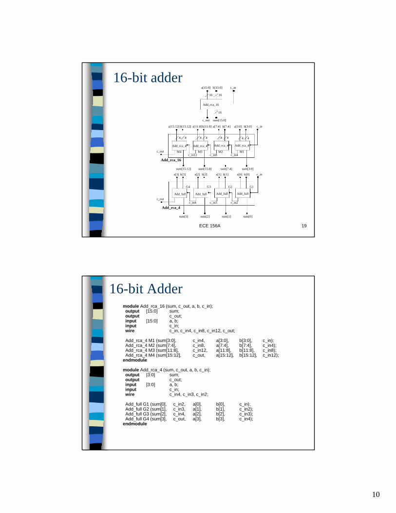
ECE 156A 19
16-bit addera[15:0] b[15:0] c_in
sum[15:0]c_out
Add_rca_16
16 16
16
a[15:12] b[15:12] a[11:8]b[11:8] a[7:4] b[7:4] a[3:0] b[3:0] c_in
sum[15:12] sum[15:8] sum[7:4] sum[3:0]
Add_rca_4Add_rca_4Add_rca_4Add_rca_4
4 4 4 4 4 4 4 4
c_in12 c_in8 c_in4c_out
Add_rca_16
sum[3] sum[2] sum[1] sum[0]
c_in4 c_in3 c_in2c_out
Add_rca_4
a[3] b[3] a[2] b[2] a[1] b[1] a[0] b[0] c_in
Add_fullAdd_fullAdd_fullAdd_full
M1M2M3M4
G1G2G3G4
16-bit Addermodule Add_rca_16 (sum, c_out, a, b, c_in);output [15:0] sum;output c_out;input [15:0] a, b;input c_in;wire c_in, c_in4, c_in8, c_in12, c_out;
Add_rca_4 M1 (sum[3:0], c_in4, a[3:0], b[3:0], c_in);Add_rca_4 M2 (sum[7:4], c_in8, a[7:4], b[7:4], c_in4);Add_rca_4 M3 (sum[11:8], c_in12, a[11:8], b[11:8], c_in8);Add_rca_4 M4 (sum[15:12], c_out, a[15:12], b[15:12], c_in12);
endmodule
module Add_rca_4 (sum, c_out, a, b, c_in);output [3:0] sum;output c_out;input [3:0] a, b;input c_in;wire c_in4, c_in3, c_in2;
Add_full G1 (sum[0], c_in2, a[0], b[0], c_in);Add_full G2 (sum[1], c_in3, a[1], b[1], c_in2);Add_full G3 (sum[2], c_in4, a[2], b[2], c_in3);Add_full G4 (sum[3], c_out, a[3], b[3], c_in4);
endmodule
11
ECE 156A 21
The concept of Design EntryDesign Entry– The entry point to do your design– Select design data representation(s)
• Behavior, RTL, Gate-Transistor Schematics
Schematic– Draw your design with gates/transistors/lines– For high-performance blocks
Hardware Description Language– Describe your design with Verilog/VHDL– Just like writing a program– No need to worry about structural detail
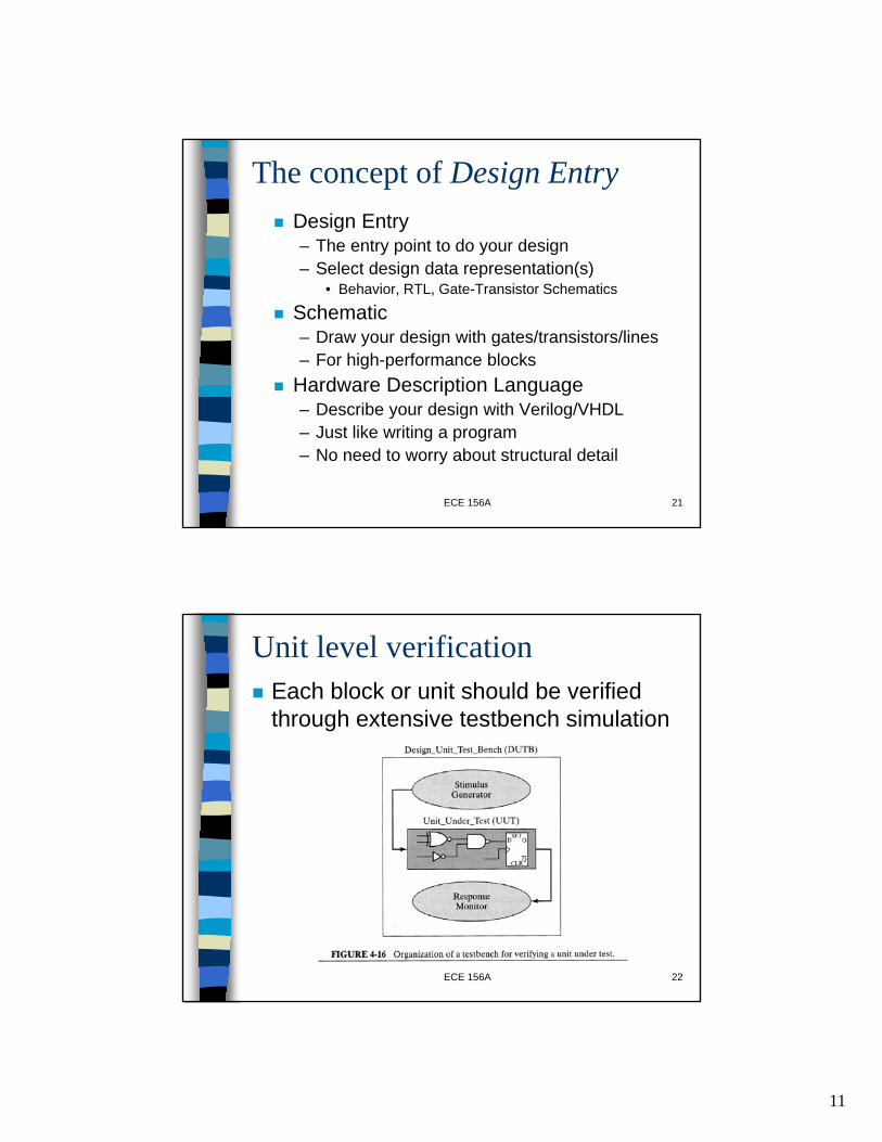
Unit level verificationEach block or unit should be verified through extensive testbench simulation
ECE 156A 22

12
A testbench example
ECE 156A 23
Generic testbench design
New version of Verilog has a lot more features to support testbench development
ECE 156A 24

13
ECE 156A 25
Delay model in verilog
These delays have no physical meaning– They are used only for simulation– The ordering of events is what being specified
• Not the actual timing– Relative delays are more important than absolute
numbers
module Add_half_1 (sum, c_out, a, b);input a, b;output sum, c_out;wire c_out_bar;
xor #2 (sum, a, b);nand #2 (c_out_bar, a, b);not #1 (c_out, c_out_bar);
endmodule
ECE 156A 26
Cell Delay Characterization
The delays are only estimations– Maybe from SPICE simulation of the actual layout
This can only be done for very small cells
module and123 (o, a, b);input a, b;output o;and (o, a, b);
specifyspecparam
Tpd_0_1 = 1.13, 3.09, 7.75Tpd_1_0 = 0.93, 2.50, 7.34
(a => o) = (Tpd_0_1, Tpd_1_0);(b => o) = (Tpd_0_1, Tpd_1_0);
endspecifyendmodule

14
Inertial delay concept
In the upper example, the event of rising transition is de-scheduled by the simulator because the pulse width is less than the propagation delay
ECE 156A 27
User-defined primitives
Basic constructs in your designContain detailed table-like descriptionUse the keywords– primitive– endprimitive
Differentiate themselves from Modules– In test, verification, and simulation, never
goes inside primitives (black-boxes)
15
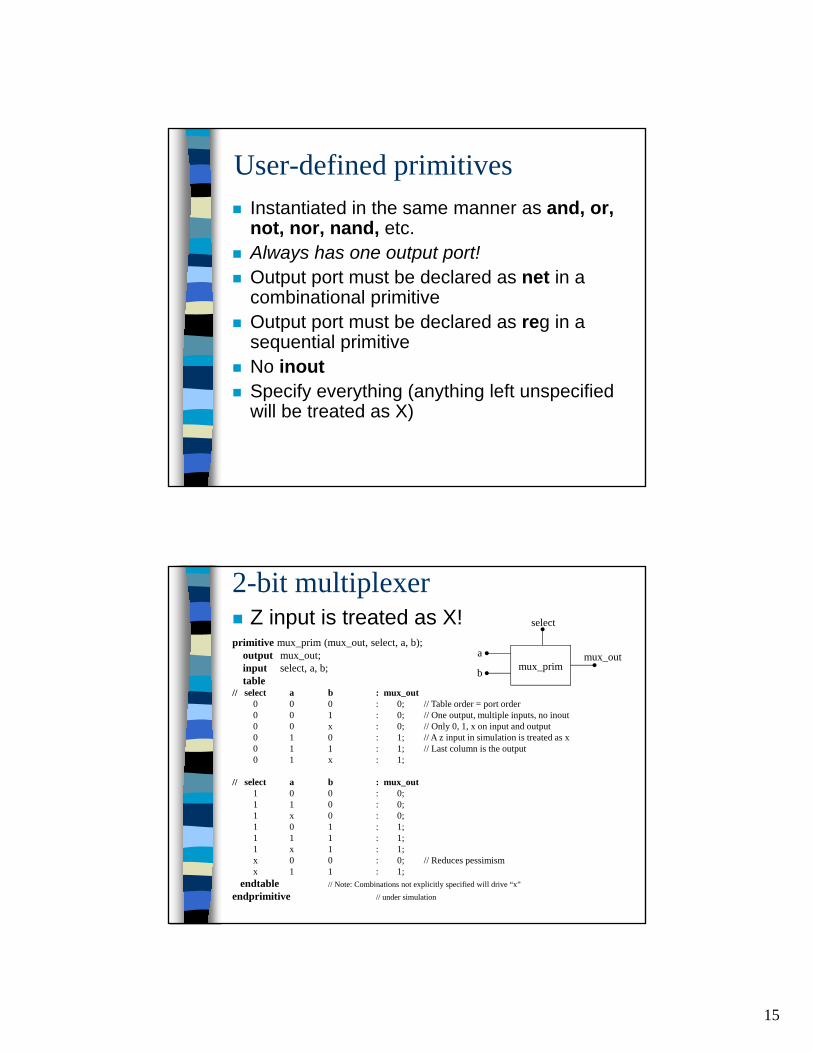
User-defined primitivesInstantiated in the same manner as and, or, not, nor, nand, etc.Always has one output port!Output port must be declared as net in a combinational primitiveOutput port must be declared as reg in a sequential primitiveNo inoutSpecify everything (anything left unspecified will be treated as X)
2-bit multiplexerZ input is treated as X!
primitive mux_prim (mux_out, select, a, b);output mux_out;input select, a, b;table
// select a b : mux_out0 0 0 : 0; // Table order = port order0 0 1 : 0; // One output, multiple inputs, no inout0 0 x : 0; // Only 0, 1, x on input and output0 1 0 : 1; // A z input in simulation is treated as x0 1 1 : 1; // Last column is the output0 1 x : 1;
// select a b : mux_out1 0 0 : 0;1 1 0 : 0;1 x 0 : 0;1 0 1 : 1;1 1 1 : 1;1 x 1 : 1;x 0 0 : 0; // Reduces pessimismx 1 1 : 1;
endtable // Note: Combinations not explicitly specified will drive “x”endprimitive // under simulation
mux_prim
select
mux_outa
b
16
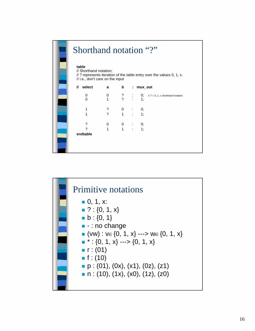
Shorthand notation “?”table// Shorthand notation;// ? represents iteration of the table entry over the values 0, 1, x.// i.e., don’t care on the input
// select a b : mux_out
0 0 ? : 0; // ? = 0, 1, x shorthand notation0 1 ? : 1;
1 ? 0 : 0;1 ? 1 : 1;
? 0 0 : 0;? 1 1 : 1;
endtable
Primitive notations0, 1, x:? : {0, 1, x}b : {0, 1}- : no change(vw) : v∈{0, 1, x} ---> w∈{0, 1, x}* : {0, 1, x} ---> {0, 1, x}r : (01)f : (10)p : (01), (0x), (x1), (0z), (z1)n : (10), (1x), (x0), (1z), (z0)

17
Sequential Primitivesn inputs1 state and 1 outputn+2 columns– <n inputs>, <state>, <output>=<next state>
Two types:– Level sensitive
• Achieve transparent latch (a latch can be made “invisible”)
– Edge sensitive
A Transparent Latch
Transparent Latch
enable
q_outdata
primitive latch (q_out, enable, data);output q_out;input enable, data;reg q_out;
table// en data state: q_out/next state
1 1 : ? : 1;1 0 : ? : 0;0 ? : ? : -;
// Note: ‘-’ denotes “no change.”// The state is the residual value of q_out
endtable // Note: Combinations not explicitly specified will drive “x”endprimitive // under simulation
tsim
tsim
tsim
1
1
1
0 10 20 30 40 50
0 10 20 30 40 50
0 10 20 30 40 50
data
enable
q_out
18
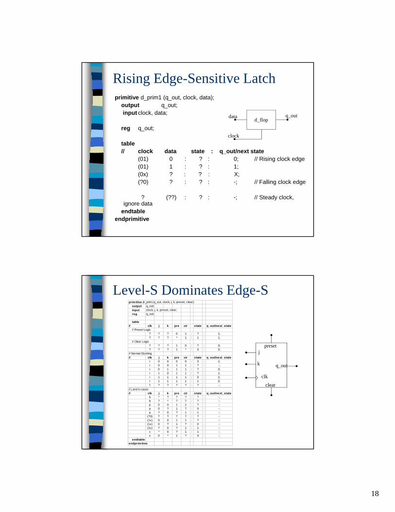
Rising Edge-Sensitive Latchprimitive d_prim1 (q_out, clock, data);
output q_out;input clock, data;
reg q_out;
table// clock data state : q_out/next state
(01) 0 : ? : 0; // Rising clock edge(01) 1 : ? : 1;(0x) ? : ? : X;(?0) ? : ? : -; // Falling clock edge
? (??) : ? : -; // Steady clock, ignore data
endtableendprimitive
d_flop
clock
q_outdata
Level-S Dominates Edge-Sprimitive jk_prim (q_out, clock, j, k, preset, clear); output q_out; input clock, j, k, preset, clear; reg q_out;
table// clk j k pre cir state q_out/next_state // Preset Logic
? ? ? 0 1 : ? : 1;? ? ? * 1 : 1 : 1;
// Clear Logic? ? ? 1 0 : ? : 0;? ? ? 1 * : 0 : 0;
// Normal Clocking// clk j k pre cir state q_out/next_state
r 0 0 0 0 : 0 : 1;r 0 0 1 1 : ? : -;r 0 1 1 1 : ? : 0;r 1 0 1 1 : ? : 1;r 1 1 1 1 : 0 : 1;r 1 1 1 1 : 1 : 0;f ? ? ? ? : ? : -;
// j and k cases// clk j k pre cir state q_out/next_state
b * ? ? ? : ? : -;b ? * ? ? : ? : -:p 0 0 1 1 : ? : -:p 0 ? 1 ? : 0 : -:p ? 0 ? 1 : 1 : -:
(?0) ? ? ? ? : ? : -:(1x) 0 0 1 1 : ? : -:(1x) 0 ? 1 ? : 0 : -:(1x) ? 0 ? 1 : 1 : -:
x * 0 ? 1 : 1 : -:x 0 * 1 ? : 0 : -:
endtableendprimitive
presetj
k
clear
q_out
clk
19
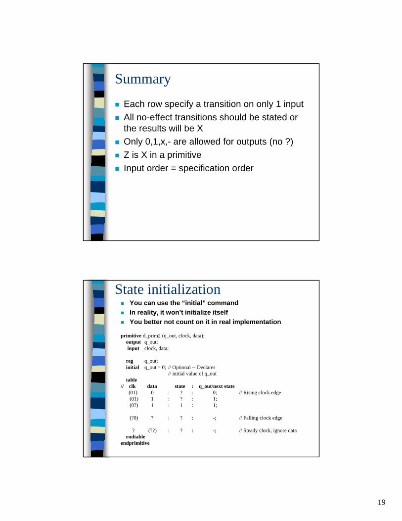
SummaryEach row specify a transition on only 1 inputAll no-effect transitions should be stated or the results will be XOnly 0,1,x,- are allowed for outputs (no ?)Z is X in a primitiveInput order = specification order
State initializationYou can use the “initial” commandIn reality, it won’t initialize itselfYou better not count on it in real implementation
primitive d_prim2 (q_out, clock, data);output q_out;input clock, data;
reg q_out;initial q_out = 0; // Optional -- Declares
// initial value of q_outtable
// clk data state : q_out/next state(01) 0 : ? : 0; // Rising clock edge(01) 1 : ? : 1;(0?) 1 : 1 : 1;
(?0) ? : ? : -; // Falling clock edge
? (??) : ? : -; // Steady clock, ignore dataendtable
endprimitive