introduction to the rf module
TRANSCRIPT
INTRODUCTION TO
RF Module

C o n t a c t I n f o r m a t i o nVisit the Contact COMSOL page at www.comsol.com/contact to submit general inquiries, contact
Technical Support, or search for an address and phone number. You can also visit the Worldwide
Sales Offices page at www.comsol.com/contact/offices for address and contact information.
If you need to contact Support, an online request form is located at the COMSOL Access page at
www.comsol.com/support/case. Other useful links include:
• Support Center: www.comsol.com/support
• Product Download: www.comsol.com/product-download
• Product Updates: www.comsol.com/support/updates
• COMSOL Blog: www.comsol.com/blogs
• Discussion Forum: www.comsol.com/community
• Events: www.comsol.com/events
• COMSOL Video Gallery: www.comsol.com/video
• Support Knowledge Base: www.comsol.com/support/knowledgebase
Part number. CM021004
I n t r o d u c t i o n t o t h e R F M o d u l e© 1998–2018 COMSOL
Protected by patents listed on www.comsol.com/patents, and U.S. Patents 7,519,518; 7,596,474; 7,623,991; 8,457,932; 8,954,302; 9,098,106; 9,146,652; 9,323,503; 9,372,673; and 9,454,625. Patents pending.
This Documentation and the Programs described herein are furnished under the COMSOL Software License Agreement (www.comsol.com/comsol-license-agreement) and may be used or copied only under the terms of the license agreement.
COMSOL, the COMSOL logo, COMSOL Multiphysics, COMSOL Desktop, COMSOL Server, and LiveLink are either registered trademarks or trademarks of COMSOL AB. All other trademarks are the property of their respective owners, and COMSOL AB and its subsidiaries and products are not affiliated with, endorsed by, sponsored by, or supported by those trademark owners. For a list of such trademark owners, see www.comsol.com/trademarks.
Version: COMSOL 5.4

Contents
Introduction . . . . . . . . . . . . . . . . . . . . . . . . . . . . . . . . . . . . . . . . . . . 5
The Use of the RF Module . . . . . . . . . . . . . . . . . . . . . . . . . . . . . . . . . 6
The RF Module Physics Interfaces . . . . . . . . . . . . . . . . . . . . . . . . 11
Physics Interface Guide by Space Dimension and Study Type . . . 14
Tutorial Example: Impedance Matching of a Lossy Ferrite
3-port Circulator . . . . . . . . . . . . . . . . . . . . . . . . . . . . . . . . . . . . . . 16
Introduction . . . . . . . . . . . . . . . . . . . . . . . . . . . . . . . . . . . . . . . . . . . . . 16
Impedance Matching. . . . . . . . . . . . . . . . . . . . . . . . . . . . . . . . . . . . . . 17
Model Definition . . . . . . . . . . . . . . . . . . . . . . . . . . . . . . . . . . . . . . . . . 17
The Lossy Ferrite Material Model . . . . . . . . . . . . . . . . . . . . . . . . . . . 17
References . . . . . . . . . . . . . . . . . . . . . . . . . . . . . . . . . . . . . . . . . . . . . . 19
| 3

4 |
Introduction
The RF Module is used by engineers and scientists to understand, predict, and design electromagnetic wave propagation and resonance effects in high-frequency applications. Simulations of this kind result in more powerful and efficient products and engineering methods. It allows its users to quickly and accurately predict electromagnetic field distributions, transmission, reflection, and power dissipation in a proposed design. Compared to traditional prototyping, it offers the benefits of lower cost and the ability to evaluate and predict entities that are not directly measurable in experiments. It also allows the exploration of operating conditions that would destroy a real prototype or be hazardous.This module covers electromagnetic fields and waves in two-dimensional and three-dimensional spaces along with traditional circuit-based modeling of passive and active devices. All modeling formulations are based on Maxwell’s equations or subsets and special cases of these together with material constitutive relations for propagation in various media. The modeling capabilities are accessed via predefined physics interfaces, referred to as Radio Frequency (RF) interfaces, which allow you to set up and solve electromagnetic models. The RF interfaces cover the modeling of electromagnetic fields and waves in frequency domain, time domain, eigenfrequency, and mode analysis.Under the hood, the RF interfaces formulate and solve the differential form of Maxwell’s equations together with the initial and boundary conditions. The equations are solved using the finite element method with numerically stable edge element discretization in combination with state-of-the-art algorithms for preconditioning and solution of the resulting sparse equation systems. The results are presented using predefined plots of electric and magnetic fields, S-parameters, power flow, and dissipation. You can also display your results as plots of expressions of the physical quantities that you define freely, or as tabulated derived values obtained from the simulation.The work flow is straightforward and can be described by the following steps: define the geometry, select materials, select a suitable RF interface, define boundary and initial conditions, define the finite element mesh, select a solver, and visualize the results. All these steps are accessed from the COMSOL Desktop. The solver selection step is usually carried out automatically using default settings, which are tuned for each specific RF interface.The RF Module’s application library describes the physics interfaces and the different features through tutorial and benchmark examples for the different formulations. The library includes antennas, ferrite devices, microwave heating phenomena, passive devices, scattering and RCS analysis, transmission lines and
| 5
waveguides in RF and microwave engineering, tutorial models for education, and benchmark models for verification and validation of the RF interfaces.This introduction is intended to give you a jump start in your modeling work. It has examples of the typical use of the RF Module, a list of the physics interfaces with a short description, and a tutorial example that introduces the modeling workflow.
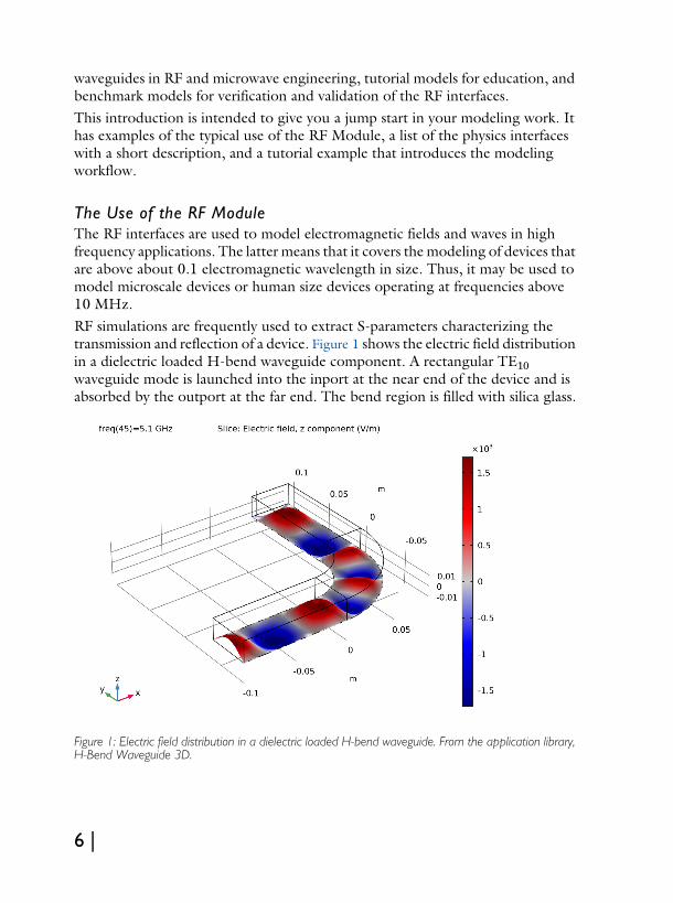
The Use of the RF ModuleThe RF interfaces are used to model electromagnetic fields and waves in high frequency applications. The latter means that it covers the modeling of devices that are above about 0.1 electromagnetic wavelength in size. Thus, it may be used to model microscale devices or human size devices operating at frequencies above 10 MHz.RF simulations are frequently used to extract S-parameters characterizing the transmission and reflection of a device. Figure 1 shows the electric field distribution in a dielectric loaded H-bend waveguide component. A rectangular TE10 waveguide mode is launched into the inport at the near end of the device and is absorbed by the outport at the far end. The bend region is filled with silica glass.
Figure 1: Electric field distribution in a dielectric loaded H-bend waveguide. From the application library, H-Bend Waveguide 3D.
6 |
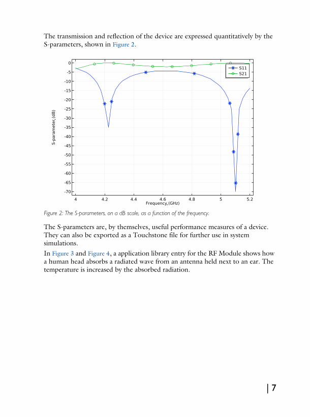
The transmission and reflection of the device are expressed quantitatively by the S-parameters, shown in Figure 2.
Figure 2: The S-parameters, on a dB scale, as a function of the frequency.
The S-parameters are, by themselves, useful performance measures of a device. They can also be exported as a Touchstone file for further use in system simulations.In Figure 3 and Figure 4, a application library entry for the RF Module shows how a human head absorbs a radiated wave from an antenna held next to an ear. The temperature is increased by the absorbed radiation.
| 7
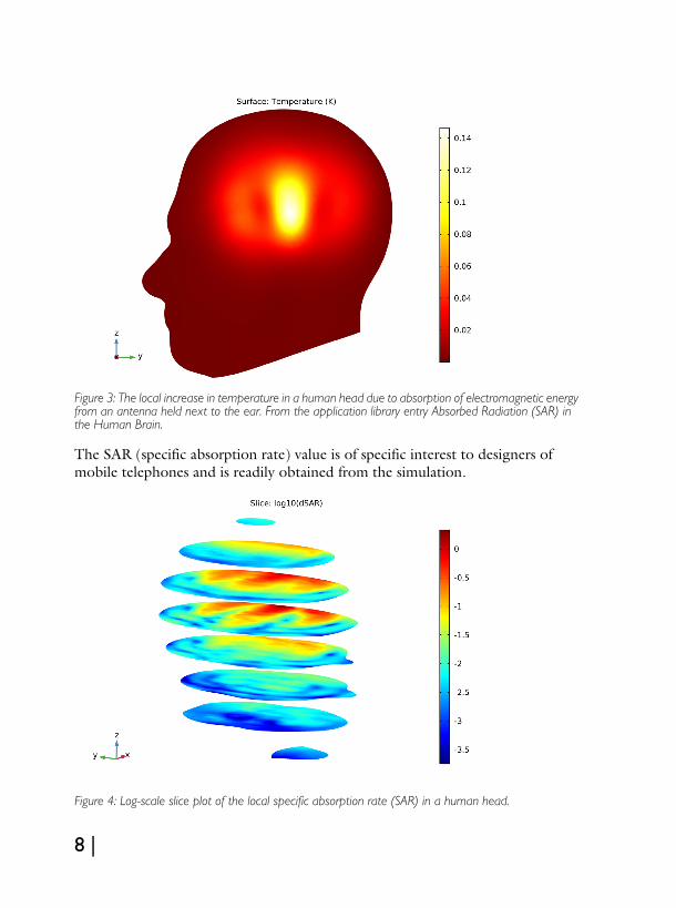
Figure 3: The local increase in temperature in a human head due to absorption of electromagnetic energy from an antenna held next to the ear. From the application library entry Absorbed Radiation (SAR) in the Human Brain.
The SAR (specific absorption rate) value is of specific interest to designers of mobile telephones and is readily obtained from the simulation.
Figure 4: Log-scale slice plot of the local specific absorption rate (SAR) in a human head.
8 |
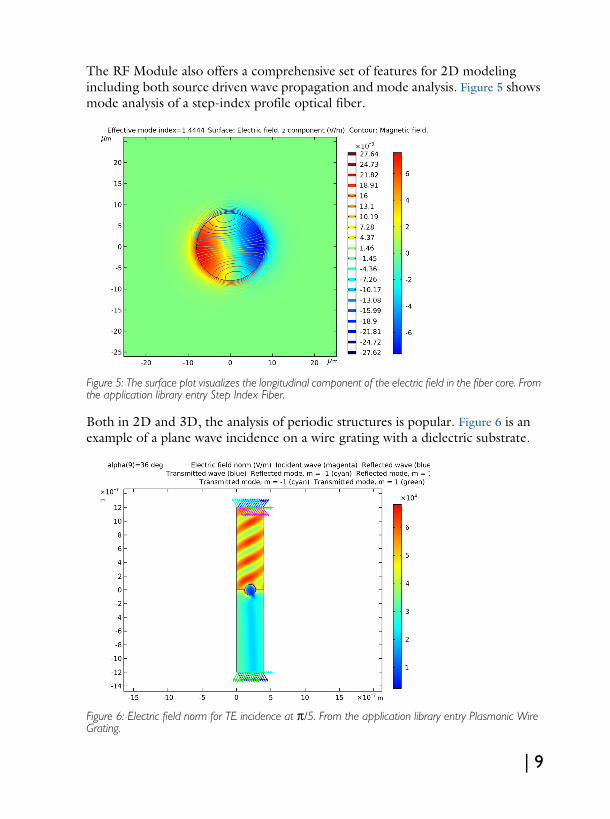
The RF Module also offers a comprehensive set of features for 2D modeling including both source driven wave propagation and mode analysis. Figure 5 shows mode analysis of a step-index profile optical fiber.
Figure 5: The surface plot visualizes the longitudinal component of the electric field in the fiber core. From the application library entry Step Index Fiber.
Both in 2D and 3D, the analysis of periodic structures is popular. Figure 6 is an example of a plane wave incidence on a wire grating with a dielectric substrate.
Figure 6: Electric field norm for TE incidence at π/5. From the application library entry Plasmonic Wire Grating.
| 9

It is also possible to perform Body-of-Revolution (BOR) simulations in 2D axisymmetry. Figure 7 illustrates the modeling of a monoconical antenna with a coaxial feed.
Figure 7: Axisymmetric model of a monoconical antenna with a coaxial feed. The azimuthal component of the magnetic field is shown. From the application library entry Conical Antenna.
The RF Module has a vast range of tools to evaluate and export the results, for example, evaluation of far-field, feed impedance, and scattering matrices (S-parameters). S-parameters can be exported in the Touchstone file format.Full-wave electromagnetic field modeling can also be combined with circuit-based modeling. This is an ideal basis for design, exploration, and optimization. More complex system models can be exploited using circuit-based modeling while maintaining links to full field models for key devices in the circuit allows for design innovation and optimization on both levels.
10 |
The RF Module Physics Interfaces
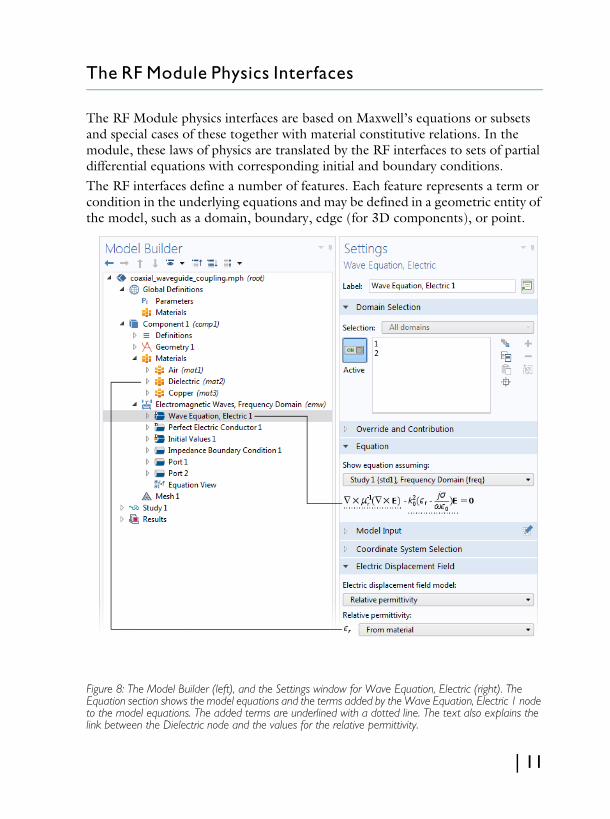
The RF Module physics interfaces are based on Maxwell’s equations or subsets and special cases of these together with material constitutive relations. In the module, these laws of physics are translated by the RF interfaces to sets of partial differential equations with corresponding initial and boundary conditions.The RF interfaces define a number of features. Each feature represents a term or condition in the underlying equations and may be defined in a geometric entity of the model, such as a domain, boundary, edge (for 3D components), or point.
Figure 8: The Model Builder (left), and the Settings window for Wave Equation, Electric (right). The Equation section shows the model equations and the terms added by the Wave Equation, Electric 1 node to the model equations. The added terms are underlined with a dotted line. The text also explains the link between the Dielectric node and the values for the relative permittivity.
| 11
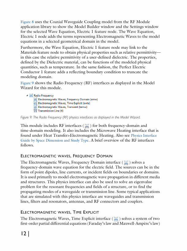
Figure 8 uses the Coaxial Waveguide Coupling model from the RF Module application library to show the Model Builder window and the Settings window for the selected Wave Equation, Electric 1 feature node. The Wave Equation, Electric 1 node adds the terms representing Electromagnetic Waves to the model equations in a selected geometrical domain in the model.Furthermore, the Wave Equation, Electric 1 feature node may link to the Materials feature node to obtain physical properties such as relative permittivity—in this case the relative permittivity of a user-defined dielectric. The properties, defined by the Dielectric material, can be functions of the modeled physical quantities, such as temperature. In the same fashion, the Perfect Electric Conductor 1 feature adds a reflecting boundary condition to truncate the modeling domain.Figure 9 shows the Radio Frequency (RF) interfaces as displayed in the Model Wizard for this module.
Figure 9: The Radio Frequency (RF) physics interfaces as displayed in the Model Wizard.
This module includes RF interfaces ( ) for both frequency-domain and time-domain modeling. It also includes the Microwave Heating interface that is found under Heat Transfer>Electromagnetic Heating. Also see Physics Interface Guide by Space Dimension and Study Type. A brief overview of the RF interfaces follows.
ELECTROMAGNETIC WAVES, FREQUENCY DOMAIN
The Electromagnetic Waves, Frequency Domain interface ( ) solves a frequency-domain wave equation for the electric field. The sources can be in the form of point dipoles, line currents, or incident fields on boundaries or domains. It is used primarily to model electromagnetic wave propagation in different media and structures. This physics interface can also be used to solve an eigenvalue problem for the resonant frequencies and fields of a structure, or to find the propagating modes of a waveguide or transmission line. Some typical applications that are simulated with this physics interface are waveguides and transmission lines, filters and resonators, antennas, and RF connectors and couplers.
ELECTROMAGNETIC WAVES, TIME EXPLICIT
The Electromagnetic Waves, Time Explicit interface ( ) solves a system of two first-order partial differential equations (Faraday’s law and Maxwell-Ampère’s law)
12 |
for the electric and magnetic fields using the Time Explicit Discontinuous Galerkin method. The sources can be in the form of volumetric electric or magnetic currents or electric surface currents or fields on boundaries. It is used primarily to model electromagnetic wave propagation in linear media. Typical applications involve the transient propagation of electromagnetic pulses.
ELECTROMAGNETIC WAVES, TRANSIENT
The Electromagnetic Waves, Transient interface ( ) solves a time-domain wave equation for the electric field. The sources can be in the form of point dipoles, line currents, or incident fields on boundaries or domains. It is used primarily to model electromagnetic wave propagation in different media and structures when a time-domain solution is required—for example, non-sinusoidal waveforms or nonlinear media. Typical applications involve the propagation of electromagnetic pulses and the generation of harmonics in nonlinear optical media.
TRANSMISSION LINE
The Transmission Line interface ( ) solves the time-harmonic transmission line equation for the electric potential. This physics interface is used when solving for electromagnetic wave propagation along one-dimensional transmission lines and is available in 1D, 2D and 3D. Eigenfrequency and Frequency Domain study types are available. The frequency domain study is used for source-driven simulations at a single frequency or a sequence of frequencies. Typical applications involve the design of impedance matching elements and networks.
MICROWAVE HEATING
The Microwave Heating interface ( ) combines the features of the Electromagnetic Waves, Frequency Domain interface with those of the Heat Transfer interface. A predefined interaction automatically sets the electromagnetic losses as sources for the heat equation. This physics interface is based on the assumption that the electromagnetic cycle time is short compared to the thermal time scale (adiabatic assumption).
ELECTRICAL CIRCUIT
The Electrical Circuit interface ( ) can be connected to an RF interface. The lumped voltage and current variables from the circuits are translated into boundary conditions applied to the distributed field model. Typical applications include the modeling of transmission lines and antenna feeding.
| 13
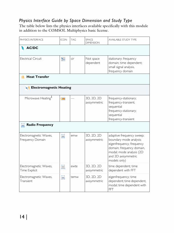
Physics Interface Guide by Space Dimension and Study TypeThe table below lists the physics interfaces available specifically with this module in addition to the COMSOL Multiphysics basic license.
PHYSICS INTERFACE ICON TAG SPACE DIMENSION
AVAILABLE STUDY TYPE
AC/DC
Electrical Circuit cir Not space dependent
stationary; frequency domain; time dependent; small signal analysis, frequency domain
Heat Transfer
Electromagnetic Heating
Microwave Heating1 — 3D, 2D, 2D axisymmetric
frequency-stationary; frequency-transient; sequential frequency-stationary; sequential frequency-transient
Radio Frequency
Electromagnetic Waves, Frequency Domain
emw 3D, 2D, 2D axisymmetric
adaptive frequency sweep; boundary mode analysis; eigenfrequency; frequency domain; frequency domain, modal; mode analysis (2D and 2D axisymmetric models only)
Electromagnetic Waves, Time Explicit
ewte 3D, 2D, 2D axisymmetric
time dependent; time dependent with FFT
Electromagnetic Waves, Transient
temw 3D, 2D, 2D axisymmetric
eigenfrequency; time dependent; time dependent, modal; time dependent with FFT
14 |

Transmission Line tl 3D, 2D, 1D eigenfrequency; frequency domain
1 This physics interface is a predefined multiphysics coupling that automatically adds all the physics interfaces and coupling features required.
PHYSICS INTERFACE ICON TAG SPACE DIMENSION
AVAILABLE STUDY TYPE
| 15
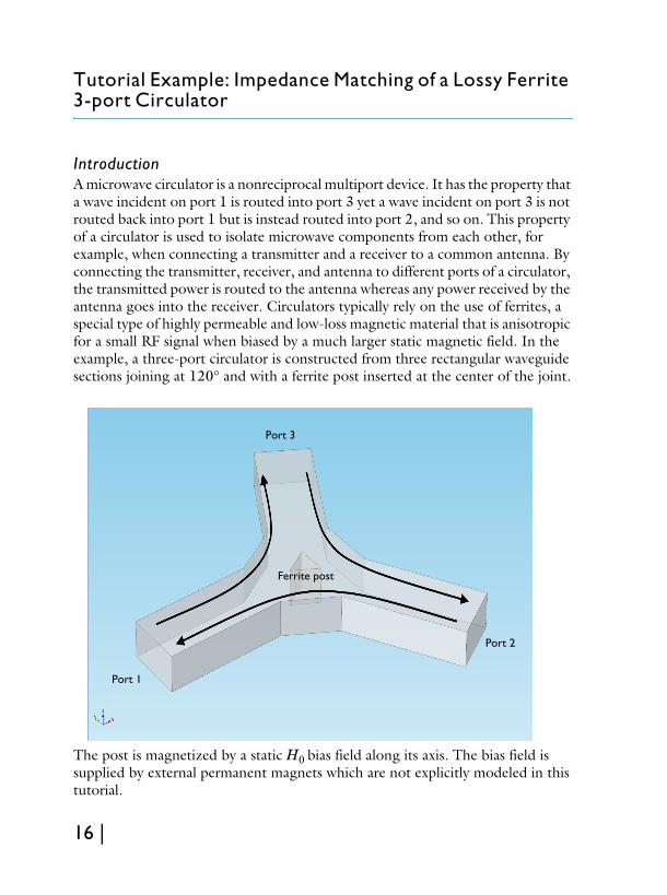
Tutorial Example: Impedance Matching of a Lossy Ferrite 3-port Circulator
IntroductionA microwave circulator is a nonreciprocal multiport device. It has the property that a wave incident on port 1 is routed into port 3 yet a wave incident on port 3 is not routed back into port 1 but is instead routed into port 2, and so on. This property of a circulator is used to isolate microwave components from each other, for example, when connecting a transmitter and a receiver to a common antenna. By connecting the transmitter, receiver, and antenna to different ports of a circulator, the transmitted power is routed to the antenna whereas any power received by the antenna goes into the receiver. Circulators typically rely on the use of ferrites, a special type of highly permeable and low-loss magnetic material that is anisotropic for a small RF signal when biased by a much larger static magnetic field. In the example, a three-port circulator is constructed from three rectangular waveguide sections joining at 120° and with a ferrite post inserted at the center of the joint.
The post is magnetized by a static H0 bias field along its axis. The bias field is supplied by external permanent magnets which are not explicitly modeled in this tutorial.
Port 3
Ferrite post
Port 1
Port 2
16 |
Impedance MatchingAn important step in the design of any microwave device is to match its input impedance for a given operating frequency. Impedance matching is equivalent to minimizing the reflections back to the inport. The parameters that need to be determined are the size of the ferrite post and the width of the wider waveguide section surrounding the ferrite. In this tutorial, these are varied in order to minimize the reflectance. The scattering parameters (S-parameters) used as measures of the reflectance and transmittance of the circulator are automatically computed.The nominal frequency for the design of the device is chosen as 3 GHz. The circulator can be expected to perform reasonably well in a narrow frequency band around 3 GHz, and so a frequency range of 2.8–3.2 GHz is studied. It is desired that the device operates in single mode. Thus a rectangular waveguide cross section of 6.67 cm by 3.33 cm is selected to set the cut-off frequency for the fundamental TE10 mode to 2.25 GHz. The cut-off frequencies for the two nearest higher modes, the TE20 and TE01 modes, are both at 4.5 GHz, leaving a reasonable safety margin.
Model DefinitionOne of the rectangular ports is excited by the fundamental TE10 mode. At the ports, the boundaries are transparent to the TE10 mode. The following equation applies to the electric field vector E inside the circulator:
where μr denotes the relative permeability tensor, ω is the angular frequency, σ is the conductivity tensor, ε0 is the permittivity of vacuum, εr is the relative permittivity tensor, and k0 is the free space wave number. In this particular model, the conductivity is zero everywhere. Losses in the ferrite are introduced as complex-valued permittivity and permeability tensors. The magnetic permeability is of key importance as it is the anisotropy of this parameter that is responsible for the nonreciprocal behavior of the circulator. For simplicity, the rather complicated material expressions are predefined in a text file that is imported into the model. The expressions are also included in the next section for reference.
The Lossy Ferrite Material ModelComplete treatises on the theory of magnetic properties of ferrites can be found in Ref. 1 and Ref. 2. The model assumes that the static magnetic bias field, H0, is much stronger than the alternating magnetic field of the microwaves, so the quoted expressions are a linearization for a small-signal analysis around this
∇ μr1– ∇ E×( )× k0
2 εrjσ
ωε0---------–
E– 0=
| 17

operating point. Under these assumptions, and including losses, the anisotropic permeability of a ferrite magnetized in the positive z direction is given by:
where
and the unique elements of the magnetic susceptibility tensor χ are given by:
where
Here μ0 denotes the permeability of free space; ω is the angular frequency of the microwave field; ω0 is the precession resonance frequency (Larmor frequency) of a spinning electron in the applied magnetic bias field, H0; ωm is the electron Larmor frequency at the saturation magnetization of the ferrite, Ms; and γ is the gyromagnetic ratio of the electron. For a lossless ferrite (α = 0), the permeability becomes infinite at ω = ω0. In a lossy ferrite (α ≠ 0), this resonance becomes finite and is broadened. The loss factor, α, is related to the line width, ΔH, of the susceptibility curve near the resonance as given by the last expression above. The material data,
Ms = 5.41·104 A/m, εr = 14.5
μ[ ]μ jκ 0jκ– μ 00 0 μ0
=
κ jμ– 0χxy=
μ μ0 1 χxx+( )=
χxxω0ωm ω0
2 ω2–( ) ω0ωmω2 α2+
ω02 ω2 1 α2+( )–( )
24ω0
2 ω2 α2+-------------------------------------------------------------------------------------- j
αωωm ω02 ω2 1 α2+( )+( )
ω02 ω2 1 α2+( )–( )
24ω0
2 ω2 α2+--------------------------------------------------------------------------------------–=
χxy2ω0ωmω2 α
ω02 ω2 1 α2+( )–( )
24ω0
2 ω2 α2+-------------------------------------------------------------------------------------- j
ωωm ω02 ω2 1 α2+( )–( )
ω02 ω2 1 α2+( )–( )
24ω0
2 ω2 α2+--------------------------------------------------------------------------------------+=
ω0 μ0γH0=
ωm μ0γMs=
αμ0γ HΔ
2ω------------------=
18 |
with an effective loss tangent of 2·10-4 and ΔH = 3.18·103 A/m, are taken for aluminum garnet from Ref. 2. The applied bias field is set to H0 = 7.96·103 A/m. The electron gyromagnetic ratio taken from Ref. 2 is 1.759·1011 C/kg.
References1. R.E. Collin, Foundations for Microwave Engineering, 2nd ed., IEEE Press/Wiley-Interscience, 2000.
2. D.M. Pozar, Microwave Engineering, 3rd ed., John Wiley & Sons Inc, 2004.
Model Wizard
These step-by-step instructions guide you through the design and modeling of the lossy three-port circulator in 3D. The first part involves the geometric design and impedance matching at a nominal frequency of 3 GHz. After that, a frequency sweep is performed to see how well it performs in a frequency band of 400 MHz centered at 3 GHz. Finally, computation and a Touchstone file export of the entire S-parameter matrix is performed.Note: These instructions are for the user interface on Windows but apply, with minor differences, also to Linux and Mac.
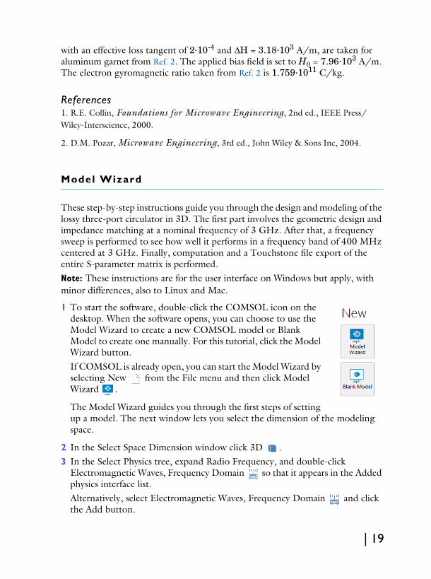
1 To start the software, double-click the COMSOL icon on the desktop. When the software opens, you can choose to use the Model Wizard to create a new COMSOL model or Blank Model to create one manually. For this tutorial, click the Model Wizard button.If COMSOL is already open, you can start the Model Wizard by selecting New from the File menu and then click Model Wizard .
The Model Wizard guides you through the first steps of setting up a model. The next window lets you select the dimension of the modeling space.
2 In the Select Space Dimension window click 3D .3 In the Select Physics tree, expand Radio Frequency, and double-click
Electromagnetic Waves, Frequency Domain so that it appears in the Added physics interface list. Alternatively, select Electromagnetic Waves, Frequency Domain and click the Add button.
| 19
4 Click Study .5 In the Studies tree under General Studies, click Frequency Domain .6 Click Done .
Global Definit ions - Parameters and Variables
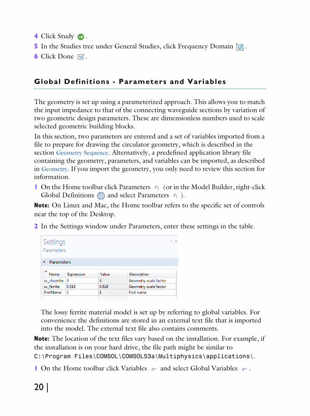
The geometry is set up using a parameterized approach. This allows you to match the input impedance to that of the connecting waveguide sections by variation of two geometric design parameters. These are dimensionless numbers used to scale selected geometric building blocks.In this section, two parameters are entered and a set of variables imported from a file to prepare for drawing the circulator geometry, which is described in the section Geometry Sequence. Alternatively, a predefined application library file containing the geometry, parameters, and variables can be imported, as described in Geometry. If you import the geometry, you only need to review this section for information.1 On the Home toolbar click Parameters (or in the Model Builder, right-click
Global Definitions and select Parameters ).Note: On Linux and Mac, the Home toolbar refers to the specific set of controls near the top of the Desktop.
2 In the Settings window under Parameters, enter these settings in the table.
The lossy ferrite material model is set up by referring to global variables. For convenience the definitions are stored in an external text file that is imported into the model. The external text file also contains comments.
Note: The location of the text files vary based on the installation. For example, if the installation is on your hard drive, the file path might be similar to C:\Program Files\COMSOL\COMSOL53a\Multiphysics\applications\.
1 On the Home toolbar click Variables and select Global Variables .
20 |
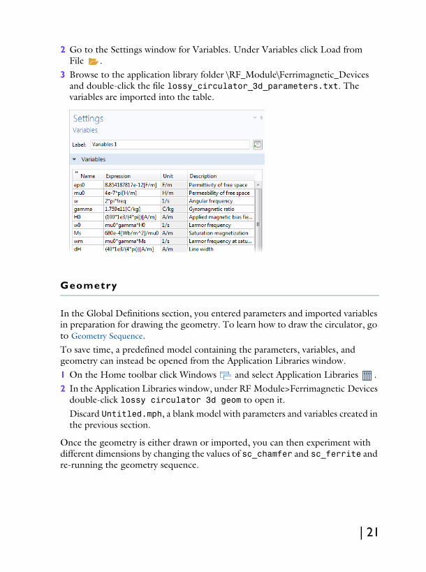
2 Go to the Settings window for Variables. Under Variables click Load from File .
3 Browse to the application library folder \RF_Module\Ferrimagnetic_Devices and double-click the file lossy_circulator_3d_parameters.txt. The variables are imported into the table.
Geometry
In the Global Definitions section, you entered parameters and imported variables in preparation for drawing the geometry. To learn how to draw the circulator, go to Geometry Sequence. To save time, a predefined model containing the parameters, variables, and geometry can instead be opened from the Application Libraries window. 1 On the Home toolbar click Windows and select Application Libraries . 2 In the Application Libraries window, under RF Module>Ferrimagnetic Devices
double-click lossy circulator 3d geom to open it. Discard Untitled.mph, a blank model with parameters and variables created in the previous section.
Once the geometry is either drawn or imported, you can then experiment with different dimensions by changing the values of sc_chamfer and sc_ferrite and re-running the geometry sequence.
| 21

Materials
The next step is to add material settings to the model. The air that fills most of the volume is available as a built-in material. The lossy ferrite has material assigned to it later, and illustrates how external material data can also be entered directly into the electromagnetic waves model. The walls of the waveguide sections are modeled as perfect conductors and do not require a material.1 On the Home toolbar click Add Material .2 In the Materials tree under Built-In, right-click Air and choose Add to
Component 1 .
3 Click Add Material again to close the Add Material window.
Electromagnetic Waves, Frequency Domain
The ferrite enters in the physics interface as a separate, user-defined equation model, referring to the global variables defined in the section Global Definitions - Parameters and Variables.
Wave Equation, Electric 21 On the Physics toolbar click Domains and choose Wave Equation,
Electric . A new node called Wave Equation, Electric 2 is added to the Model Builder. The nodes with a ‘D’ in the upper left corner indicate a default node.
2 To get a view of the interior part of the circulator, click the Wireframe Rendering button on the Graphics toolbar.
22 |

3 Select Domain 2 only.
Note: There are many ways to select geometric entities. When you know the domain to add, such as in this exercise, you can click the Paste Selection button located beside the Selection list and enter the information in the Selection text field. In this example enter 2 in the Paste Selection window. For more information about selecting geometric entities in the Graphics window, see the COMSOL Multiphysics Reference Manual.
4 Go to the Settings window for Wave Equation, Electric 2. Under Electric Displacement Field: - From the Electric displacement field
model list, select Dielectric loss.- From the ε′ list, select User defined. In
the associated text field, enter eps_r_p.- From the ε′′ list, select User defined. In
the associated text field, enter eps_r_b.
Domain 2
| 23

5 Under Magnetic Field, from the μr list, select User defined and Anisotropic.
6 In the μr table, enter the settings as in the figure to the right.
7 Under Conduction Current from the σ list, select User defined and leave the default value at 0.
Now add ports for excitation and transmission.
Port 1, Port 2, and Port 31 On the Physics toolbar click Boundaries and choose Port .2 Select Boundary 1 only.3 Go to the Settings window for Port. Under Port Properties from the Type of
port list, select Rectangular.4 From the Wave excitation at this port
list, select On.5 On the Physics toolbar click
Boundaries and choose Port to add another Port node. For Port 2:- Select Boundary 18- Select Rectangular from the Type
of port list6 Add another Port node. For Port
3:- Select Boundary 19- Select Rectangular from the Type of port list
Boundary 1Boundary 18
Boundary 19
24 |
The node sequence in the Model Builder should match this figure.
Mesh
The mesh automatically aligns to the geometry. Physics related considerations can also be incorporated into the mesh. In particular, the mesh needs to resolve the local wavelength and, for lossy domains, the skin depth. The skin depth in the ferrite is large compared to the size of the domain so the main concern is to resolve the local wavelength. This is done by providing maximum mesh sizes per domain. The rule of thumb is to use a maximum element size that is one fifth of the local wavelength (at the maximum frequency) or less.
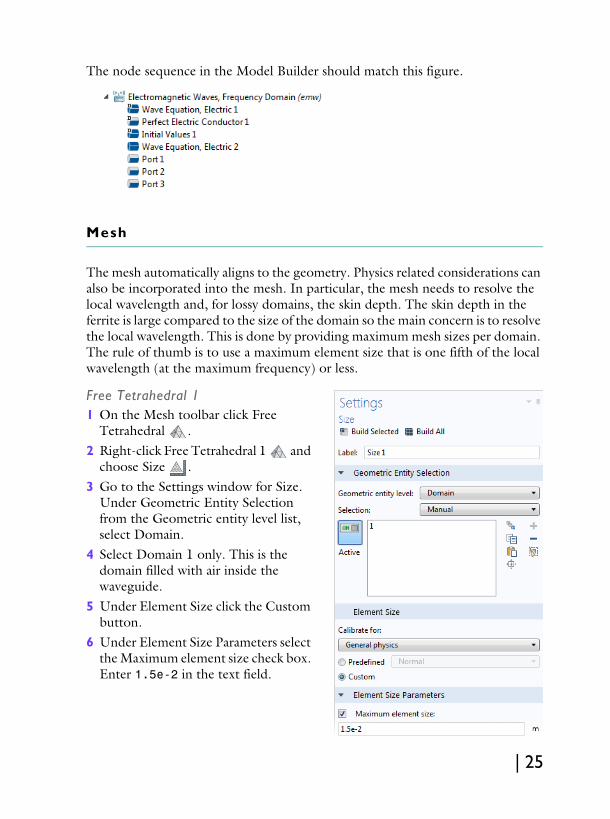
Free Tetrahedral 11 On the Mesh toolbar click Free
Tetrahedral .2 Right-click Free Tetrahedral 1 and
choose Size .3 Go to the Settings window for Size.
Under Geometric Entity Selection from the Geometric entity level list, select Domain.
4 Select Domain 1 only. This is the domain filled with air inside the waveguide.
5 Under Element Size click the Custom button.
6 Under Element Size Parameters select the Maximum element size check box. Enter 1.5e-2 in the text field.
| 25

Size 21 Right-click Free Tetrahedral 1 and choose Size . A second Size node is
added to the sequence.2 Go to the Settings window for Size. Under Geometric Entity Selection from the
Geometric entity level list, select Domain.3 Select Domain 2 only. This is the ferrite post domain.4 Under Element Size click the Custom button.5 Under Element Size Parameters select the Maximum element size check box.
Enter 4.5e-3 in the text field.6 In the Settings window for Size click Build All .
The node sequence in the Model Builder and the mesh should match the figure below.
Study 1
The final step is to solve for the nominal frequency and inspect the results for possible modeling errors.1 In the Model Builder expand the Study 1 node, then click Step 1: Frequency
Domain .2 Go to the Settings window for Frequency Domain. Under Study Settings, in the
Frequencies text field, enter 3e9.3 In the Model Builder, right-click Study 1 and choose Compute .
26 |

Results
Electric FieldThe default multislice plot shows the electric field norm. It is best viewed from above, so click the Go to XY View button on the Graphics toolbar.The electric field norm gives a good indication of where the main power is flowing and where there are standing waves due to reflections from the impedance mismatch at the center.
Definit ions - Probes
The remaining work is to vary the two design parameters to minimize reflections at the nominal frequency. To do this, perform parametric sweeps over the design parameters (scale factors). To avoid accumulating a lot of data while solving, throw away the solutions and log only the S-parameter representing reflection in a table. For this purpose, add a Global Variable Probe to the model.1 On the Definitions toolbar click Probes and select Global Variable
Probe .
| 27
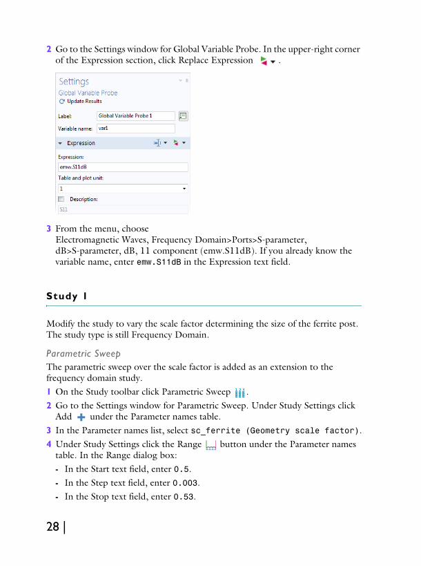
2 Go to the Settings window for Global Variable Probe. In the upper-right corner of the Expression section, click Replace Expression .
3 From the menu, choose Electromagnetic Waves, Frequency Domain>Ports>S-parameter, dB>S-parameter, dB, 11 component (emw.S11dB). If you already know the variable name, enter emw.S11dB in the Expression text field.
Study 1
Modify the study to vary the scale factor determining the size of the ferrite post. The study type is still Frequency Domain.
Parametric SweepThe parametric sweep over the scale factor is added as an extension to the frequency domain study. 1 On the Study toolbar click Parametric Sweep .2 Go to the Settings window for Parametric Sweep. Under Study Settings click
Add under the Parameter names table.3 In the Parameter names list, select sc_ferrite (Geometry scale factor).4 Under Study Settings click the Range button under the Parameter names
table. In the Range dialog box:- In the Start text field, enter 0.5.- In the Step text field, enter 0.003.- In the Stop text field, enter 0.53.
28 |
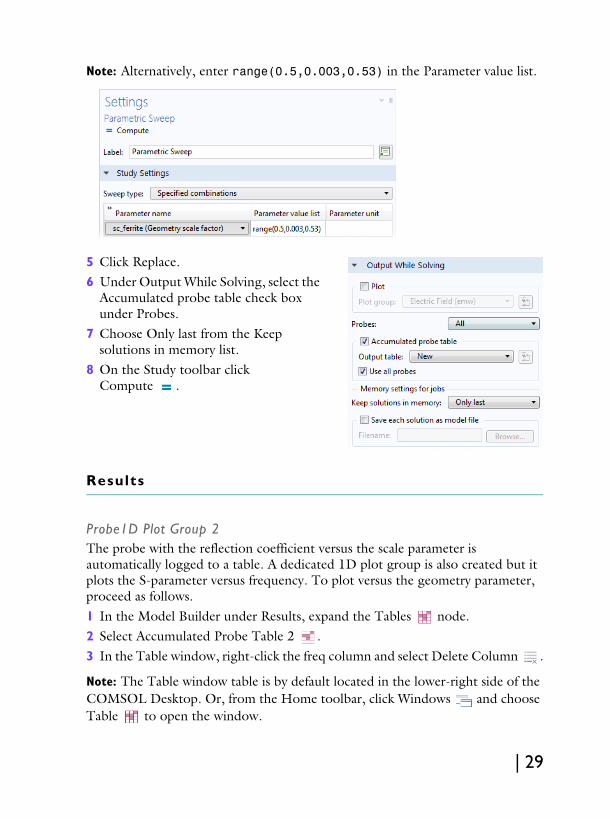
Note: Alternatively, enter range(0.5,0.003,0.53) in the Parameter value list.
5 Click Replace.6 Under Output While Solving, select the
Accumulated probe table check box under Probes.
7 Choose Only last from the Keep solutions in memory list.
8 On the Study toolbar click Compute .
Results
Probe1D Plot Group 2The probe with the reflection coefficient versus the scale parameter is automatically logged to a table. A dedicated 1D plot group is also created but it plots the S-parameter versus frequency. To plot versus the geometry parameter, proceed as follows.1 In the Model Builder under Results, expand the Tables node.2 Select Accumulated Probe Table 2 .3 In the Table window, right-click the freq column and select Delete Column .
Note: The Table window table is by default located in the lower-right side of the COMSOL Desktop. Or, from the Home toolbar, click Windows and choose Table to open the window.
| 29
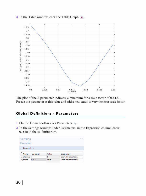
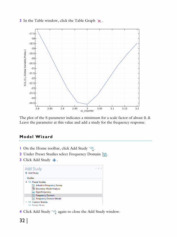
4 In the Table window, click the Table Graph .
The plot of the S-parameter indicates a minimum for a scale factor of 0.518. Freeze the parameter at this value and add a new study to vary the next scale factor.
Global Definit ions - Parameters
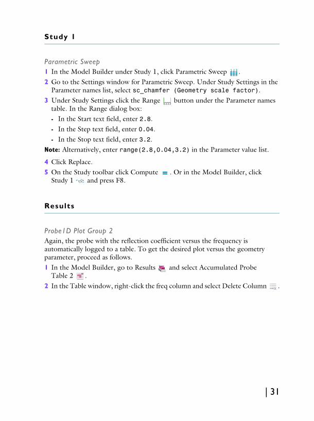
1 On the Home toolbar click Parameters .2 In the Settings window under Parameters, in the Expression column enter 0.518 in the sc_ferrite row.
30 |
Study 1
Parametric Sweep1 In the Model Builder under Study 1, click Parametric Sweep .2 Go to the Settings window for Parametric Sweep. Under Study Settings in the
Parameter names list, select sc_chamfer (Geometry scale factor).3 Under Study Settings click the Range button under the Parameter names
table. In the Range dialog box:- In the Start text field, enter 2.8.- In the Step text field, enter 0.04.- In the Stop text field, enter 3.2.
Note: Alternatively, enter range(2.8,0.04,3.2) in the Parameter value list.
4 Click Replace.5 On the Study toolbar click Compute . Or in the Model Builder, click
Study 1 and press F8.
Results
Probe1D Plot Group 2Again, the probe with the reflection coefficient versus the frequency is automatically logged to a table. To get the desired plot versus the geometry parameter, proceed as follows.1 In the Model Builder, go to Results and select Accumulated Probe
Table 2 .2 In the Table window, right-click the freq column and select Delete Column .
| 31
3 In the Table window, click the Table Graph .
The plot of the S-parameter indicates a minimum for a scale factor of about 3.0. Leave the parameter at this value and add a study for the frequency response.
Model Wizard
1 On the Home toolbar, click Add Study .2 Under Preset Studies select Frequency Domain .3 Click Add Study .
4 Click Add Study again to close the Add Study window.
32 |
Electromagnetic Waves (emw)
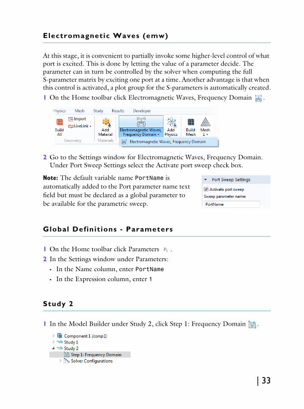
At this stage, it is convenient to partially invoke some higher-level control of what port is excited. This is done by letting the value of a parameter decide. The parameter can in turn be controlled by the solver when computing the full S-parameter matrix by exciting one port at a time. Another advantage is that when this control is activated, a plot group for the S-parameters is automatically created.1 On the Home toolbar click Electromagnetic Waves, Frequency Domain .
2 Go to the Settings window for Electromagnetic Waves, Frequency Domain. Under Port Sweep Settings select the Activate port sweep check box.
Note: The default variable name PortName is automatically added to the Port parameter name text field but must be declared as a global parameter to be available for the parametric sweep.
Global Definit ions - Parameters
1 On the Home toolbar click Parameters .2 In the Settings window under Parameters:
- In the Name column, enter PortName- In the Expression column, enter 1
Study 2
1 In the Model Builder under Study 2, click Step 1: Frequency Domain .
| 33
2 Go to the Settings window for Frequency Domain. Under Study Settings click the Range button.
3 From the Entry method list, select Number of values.- In the Start text field, enter 2.8e9.- In the Stop text field, enter 3.2e9.- In the Number of values text field, enter 21.
4 Click Replace.5 On the Study toolbar click Compute . Or click Study 2 and press F8.
Results
The probe with the reflection coefficient versus the frequency is automatically logged to a table and plotted while solving. At the last frequency, there are pronounced standing waves. Look at the center frequency instead.1 In the Model Builder under Results, click Electric Field (emw) 1 .
2 Go to the Settings window for 3D Plot Group. Under Data from the Parameter value (freq) list, select 3.
34 |

3 Click the Plot button. Click the Go to XY View button .
At the center frequency most of the standing waves are gone.
Electromagnetic Waves (emw)
Finally look at all the S-parameters plotted versus the frequency. Go to the Global 1 plot in the S-Parameter (emw) plot group and remove all S-Parameters that are not relevant. You should only display emw.S11dB, emw.S21dB, and emw.S31dB.1 In the Model Builder expand the S-Parameter (emw) node then click Global 1.2 In the Settings window for Global locate the y-Axis Data section. In the table,
select:- Row number 2. Click Delete twice.- Row number 3. Click Delete twice.- Row number 4. Click Delete twice.
| 35
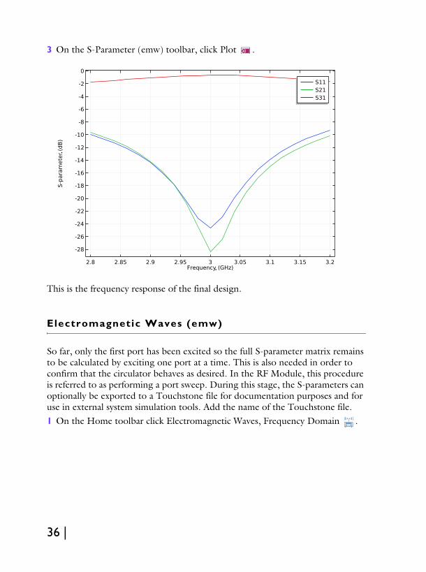
3 On the S-Parameter (emw) toolbar, click Plot .
This is the frequency response of the final design.
Electromagnetic Waves (emw)
So far, only the first port has been excited so the full S-parameter matrix remains to be calculated by exciting one port at a time. This is also needed in order to confirm that the circulator behaves as desired. In the RF Module, this procedure is referred to as performing a port sweep. During this stage, the S-parameters can optionally be exported to a Touchstone file for documentation purposes and for use in external system simulation tools. Add the name of the Touchstone file.1 On the Home toolbar click Electromagnetic Waves, Frequency Domain .
36 |

2 Go to the Settings window for Electromagnetic Waves, Frequency Domain. Under Port Sweep Settings in the Touchstone file export text field, enter: lossy_circulator_3d.s3p.
Note: The Touchstone file is saved in the start directory of COMSOL Multiphysics unless a different file path is specified with the Browse button.
Study 1
Reuse the first study for the port sweep. The study is solved for a single frequency to keep simulation time to a minimum although it is possible to solve for a range of frequencies. All solutions are needed in order to display the S-parameter matrix in a table so this setting has to be changed.
Parametric SweepThe parametric sweep is used to control which port is excited. It overrides the settings on individual port features and drives one port at a time using 1 W of input power.1 In the Model Builder under Study 1 click
Parametric Sweep .2 Go to the Settings window for Parametric Sweep.
Under Study Settings, in the Parameter names list, select PortName.
| 37
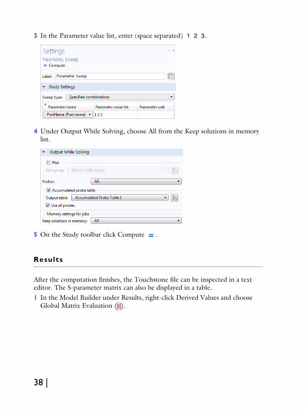
3 In the Parameter value list, enter (space separated) 1 2 3.
4 Under Output While Solving, choose All from the Keep solutions in memory list.
5 On the Study toolbar click Compute .
Results
After the computation finishes, the Touchstone file can be inspected in a text editor. The S-parameter matrix can also be displayed in a table.1 In the Model Builder under Results, right-click Derived Values and choose
Global Matrix Evaluation .
38 |
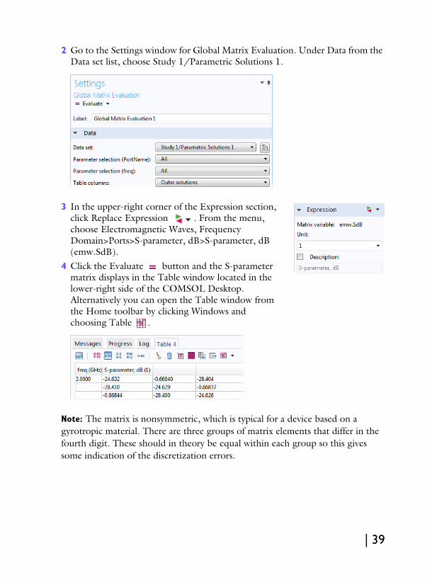
2 Go to the Settings window for Global Matrix Evaluation. Under Data from the Data set list, choose Study 1/Parametric Solutions 1.
3 In the upper-right corner of the Expression section, click Replace Expression . From the menu, choose Electromagnetic Waves, Frequency Domain>Ports>S-parameter, dB>S-parameter, dB (emw.SdB).
4 Click the Evaluate button and the S-parameter matrix displays in the Table window located in the lower-right side of the COMSOL Desktop. Alternatively you can open the Table window from the Home toolbar by clicking Windows and choosing Table .
Note: The matrix is nonsymmetric, which is typical for a device based on a gyrotropic material. There are three groups of matrix elements that differ in the fourth digit. These should in theory be equal within each group so this gives some indication of the discretization errors.
| 39
Definit ions
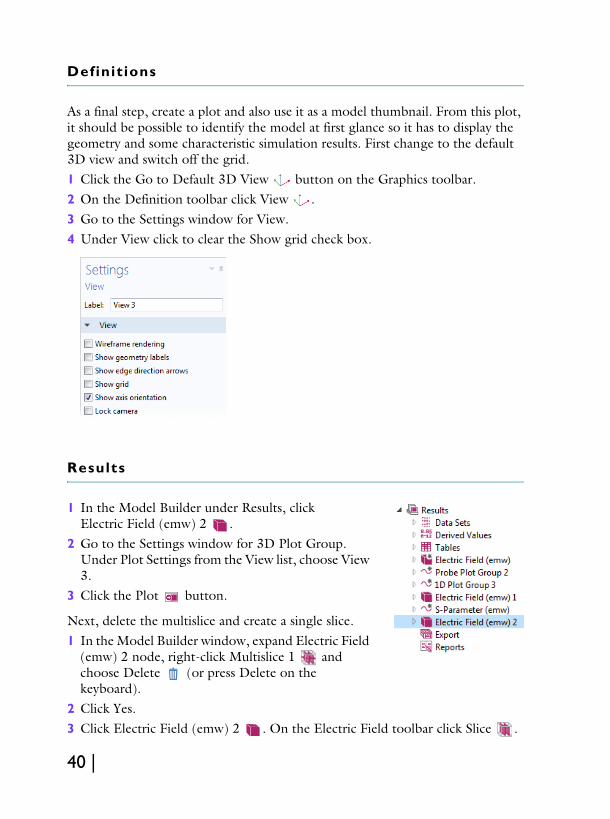
As a final step, create a plot and also use it as a model thumbnail. From this plot, it should be possible to identify the model at first glance so it has to display the geometry and some characteristic simulation results. First change to the default 3D view and switch off the grid.1 Click the Go to Default 3D View button on the Graphics toolbar.2 On the Definition toolbar click View .3 Go to the Settings window for View.4 Under View click to clear the Show grid check box.
Results
1 In the Model Builder under Results, click Electric Field (emw) 2 .
2 Go to the Settings window for 3D Plot Group. Under Plot Settings from the View list, choose View 3.
3 Click the Plot button.
Next, delete the multislice and create a single slice.1 In the Model Builder window, expand Electric Field
(emw) 2 node, right-click Multislice 1 and choose Delete (or press Delete on the keyboard).
2 Click Yes.3 Click Electric Field (emw) 2 . On the Electric Field toolbar click Slice .
40 |

4 In the Settings window for Slice under Plane data from the Plane list, choose xy-planes. In the Planes text field, enter 1
Add a deformation proportional to the electric field to the slice.1 Right-click Slice 1 and choose Deformation .2 Go to the Settings window for Deformation. In the upper-right corner of the
Expression section, click Replace Expression . From the menu, choose Electromagnetic Waves, Frequency Domain>Electric>Electric field (emw.Ex,emw.Ey,emw.Ez).
3 Under Expression select the Description check box.
Display the magnetic field as arrows. Use logarithmic length scaling to make sure that the arrows are clearly visible everywhere. Place the arrows well above the slice.1 In the Model Builder, right-click Electric Field (emw) 2 and choose Arrow
Volume .
2 Go to the Settings window for Arrow Volume. Click Replace Expression .
| 41
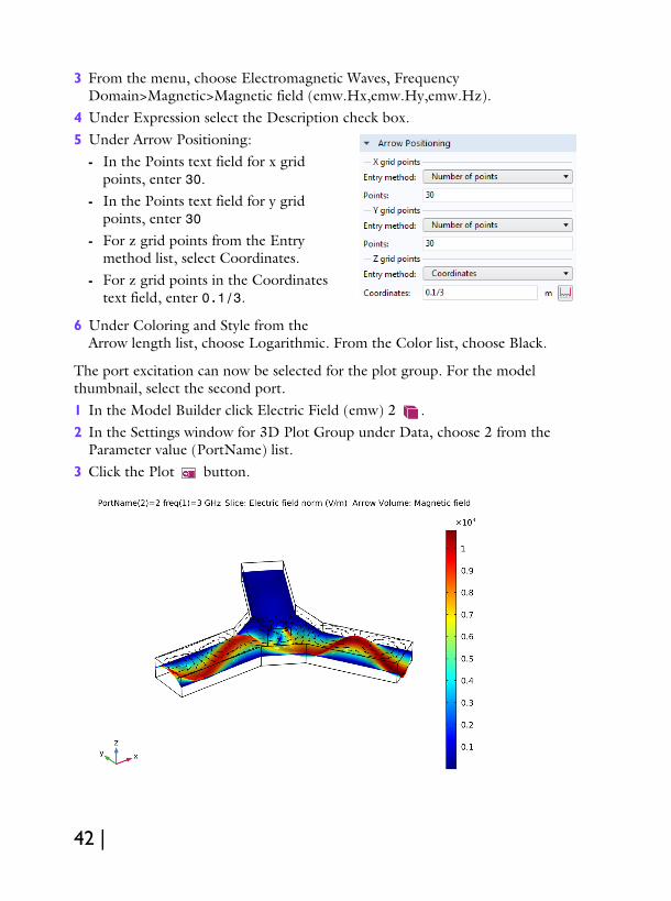
3 From the menu, choose Electromagnetic Waves, Frequency Domain>Magnetic>Magnetic field (emw.Hx,emw.Hy,emw.Hz).
4 Under Expression select the Description check box.5 Under Arrow Positioning:
- In the Points text field for x grid points, enter 30.
- In the Points text field for y grid points, enter 30
- For z grid points from the Entry method list, select Coordinates.
- For z grid points in the Coordinates text field, enter 0.1/3.
6 Under Coloring and Style from the Arrow length list, choose Logarithmic. From the Color list, choose Black.
The port excitation can now be selected for the plot group. For the model thumbnail, select the second port.1 In the Model Builder click Electric Field (emw) 2 .2 In the Settings window for 3D Plot Group under Data, choose 2 from the
Parameter value (PortName) list.3 Click the Plot button.
42 |
Select this plot to use as a model thumbnail.1 In the Model Builder under Results click Electric Field (emw) 2 .2 Click the Root node (the first node in the model tree). On the Settings window
for Root, under Presentation, click Set from Graphics Window.
This concludes the modeling session unless you want to practice drawing the “Geometry Sequence”, which continues below.
Geometry Sequence
In Global Definitions - Parameters and Variables parameters were entered to prepare for drawing the circulator geometry. Once the geometry is created, you can then experiment with different dimensions by changing the values of sc_chamfer and sc_ferrite and re-running the geometry sequence. These step-by-step instructions build the same geometry that is contained in the application library file lossy_circulator_3d_geom (imported in the section Geometry). The geometry is built by first defining a 2D cross section of the 3D geometry in a work plane. The 2D geometry is then extruded into 3D.Note: You need to complete the first two sections Model Wizard and Global Definitions - Parameters and Variables before defining the geometry.
Start by defining one arm of the circulator, then copy and rotate it twice to build all three arms.
Rectangle 11 On the Geometry toolbar click
Work Plane .2 Under Work Plane 1 right-click Plane Geometry and choose Rectangle .3 Go to the Settings window for Rectangle. Under Size:
- In the Width text field, enter 0.2-0.1/(3*sqrt(3)).- In the Height text field, enter 0.2/3.
4 Under Position: - In the xw text field, enter -0.2.- In the yw text field, enter -0.1/3.
5 Click the Build Selected button.
| 43

Copy 11 Right-click Plane Geometry and from the Transforms menu select
Copy .2 To select the object r1, move the mouse
pointer to the Graphics window and hover over the rectangle r1 so that it turns red. Then click on the rectangle when it is red so that it turns blue. The object r1 is added to the Input objects list on the Settings window for Copy. Click the Build Selected button.
Note: To turn on the geometry labels in the Graphics window, in the Model Builder under Geometry 1>WorkPlane 1>Plane Geometry, click the View 2 node. Go to the Settings window for View and select the Show geometry labels check box.
Rotate 11 Right-click Plane Geometry and from the Transforms menu select
Rotate .2 To select only the object copy1, which lies underneath the object r1, move the
mouse pointer to the Graphics window and hover over the rectangle r1 so that it turns red. While the rectangle r1 is red, use the mouse wheel and then left-click when the rectangle underneath (copy1) is selected.
3 Go to the Settings window for Rotate. Under Rotation Angle in the Rotation text field, enter 120.
44 |
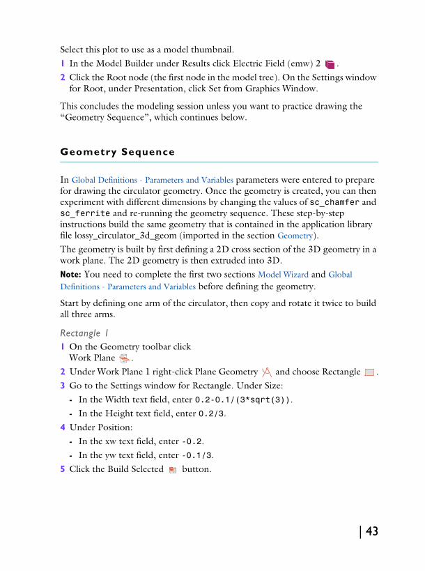
4 Click the Build Selected button and then click the Zoom Extents button on the Graphics toolbar. The geometry should match the figure so far.
Copy 21 Right-click Plane Geometry and choose Transforms>Copy .2 Select the object r1 only and add it to the Input objects list in the Settings
window for Copy.3 Click the Build Selected button.
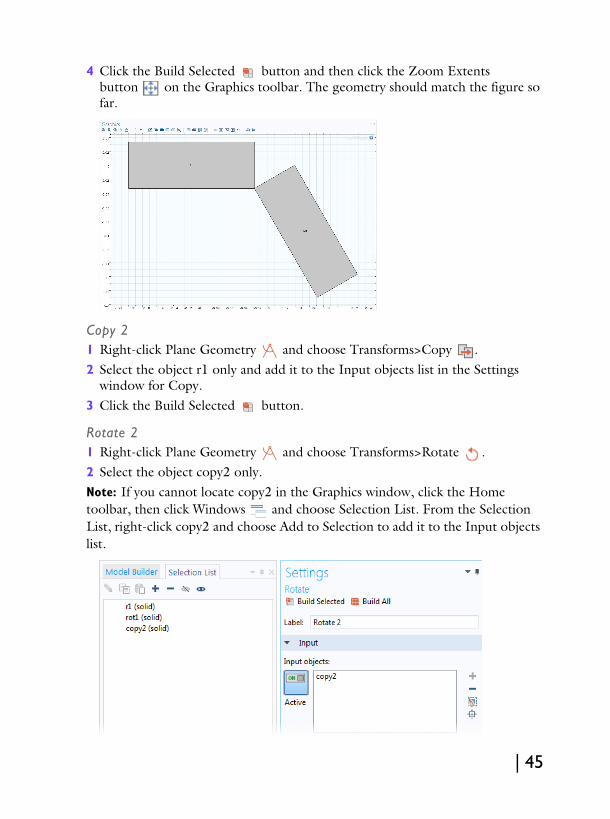
Rotate 21 Right-click Plane Geometry and choose Transforms>Rotate .2 Select the object copy2 only. Note: If you cannot locate copy2 in the Graphics window, click the Home toolbar, then click Windows and choose Selection List. From the Selection List, right-click copy2 and choose Add to Selection to add it to the Input objects list.
| 45
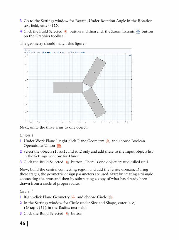
3 Go to the Settings window for Rotate. Under Rotation Angle in the Rotation text field, enter -120.
4 Click the Build Selected button and then click the Zoom Extents button on the Graphics toolbar.
The geometry should match this figure.
Next, unite the three arms to one object.
Union 11 Under Work Plane 1 right-click Plane Geometry and choose Boolean
Operations>Union .2 Select the objects r1, rot1, and rot2 only and add these to the Input objects list
in the Settings window for Union.3 Click the Build Selected button. There is one object created called uni1.
Now, build the central connecting region and add the ferrite domain. During these stages, the geometric design parameters are used. Start by creating a triangle connecting the arms and then by subtracting a copy of what has already been drawn from a circle of proper radius.
Circle 11 Right-click Plane Geometry and choose Circle .2 In the Settings window for Circle under Size and Shape, enter 0.2/(3*sqrt(3)) in the Radius text field.
3 Click the Build Selected button.
46 |
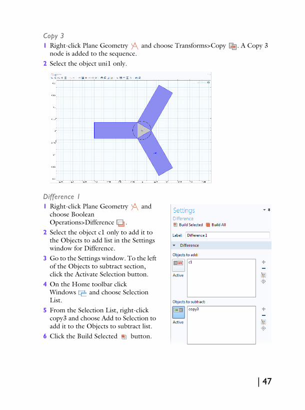
Copy 31 Right-click Plane Geometry and choose Transforms>Copy . A Copy 3
node is added to the sequence.2 Select the object uni1 only.
Difference 11 Right-click Plane Geometry and
choose Boolean Operations>Difference .
2 Select the object c1 only to add it to the Objects to add list in the Settings window for Difference.
3 Go to the Settings window. To the left of the Objects to subtract section, click the Activate Selection button.
4 On the Home toolbar click Windows and choose Selection List.
5 From the Selection List, right-click copy3 and choose Add to Selection to add it to the Objects to subtract list.
6 Click the Build Selected button.
| 47
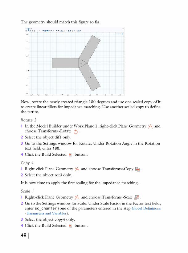
The geometry should match this figure so far.
Now, rotate the newly created triangle 180 degrees and use one scaled copy of it to create linear fillets for impedance matching. Use another scaled copy to define the ferrite.
Rotate 31 In the Model Builder under Work Plane 1, right-click Plane Geometry and
choose Transforms>Rotate .2 Select the object dif1 only.3 Go to the Settings window for Rotate. Under Rotation Angle in the Rotation
text field, enter 180.4 Click the Build Selected button.
Copy 41 Right-click Plane Geometry and choose Transforms>Copy .2 Select the object rot3 only.
It is now time to apply the first scaling for the impedance matching.
Scale 11 Right-click Plane Geometry and choose Transforms>Scale .2 Go to the Settings window for Scale. Under Scale Factor in the Factor text field,
enter sc_chamfer (one of the parameters entered in the step Global Definitions - Parameters and Variables).
3 Select the object copy4 only.4 Click the Build Selected button.
48 |

Union 21 Right-click Plane Geometry and choose Boolean Operations>Union .2 Select the objects uni1 and sca1 only. Use the Selection List to select the objects
if required.3 Go to the Settings window for Union. Under Union click to clear the Keep
interior boundaries check box.4 Click the Build Selected button.
The geometry should match this figure.
Next, apply the scaling for the ferrite region.
| 49
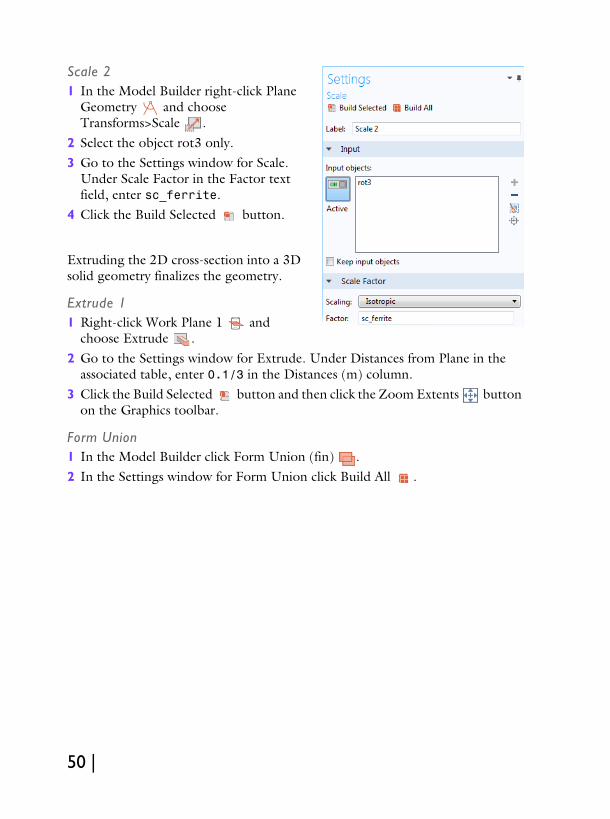
Scale 21 In the Model Builder right-click Plane
Geometry and choose Transforms>Scale .
2 Select the object rot3 only.3 Go to the Settings window for Scale.
Under Scale Factor in the Factor text field, enter sc_ferrite.
4 Click the Build Selected button.
Extruding the 2D cross-section into a 3D solid geometry finalizes the geometry.
Extrude 11 Right-click Work Plane 1 and
choose Extrude .2 Go to the Settings window for Extrude. Under Distances from Plane in the
associated table, enter 0.1/3 in the Distances (m) column.3 Click the Build Selected button and then click the Zoom Extents button
on the Graphics toolbar.
Form Union1 In the Model Builder click Form Union (fin) .2 In the Settings window for Form Union click Build All .
50 |
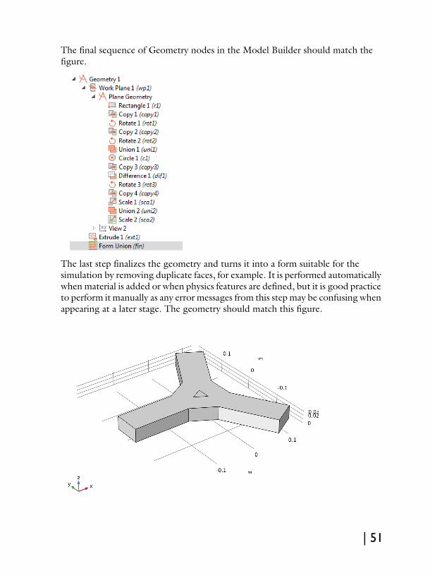
The final sequence of Geometry nodes in the Model Builder should match the figure.
The last step finalizes the geometry and turns it into a form suitable for the simulation by removing duplicate faces, for example. It is performed automatically when material is added or when physics features are defined, but it is good practice to perform it manually as any error messages from this step may be confusing when appearing at a later stage. The geometry should match this figure.
| 51

Note: If you skipped to this section to learn how to create the geometry, you can now return to the next tutorial step: Materials.
52 |