introduction to the dspic dsc smps (part 1) - microchip technology inc
TRANSCRIPT
Page 1
© 2008 Microchip Technology Incorporated. All Rights Reserved. Introduction to dsPIC® DSC SMPS Slide 1
Introduction to the dsPIC® DSC SMPS
(Part 1)
Welcome to part 1 of the Introduction to the dsPIC® DSC SMPS family web seminar. My name is Alex Dumais and I am an Applications Engineer for Microchip.
Page 2
© 2008 Microchip Technology Incorporated. All Rights Reserved. Introduction to dsPIC® DSC SMPS Slide 2
Session Agenda
� Basic dsPIC® DSC SMPS features� High-Speed Analog Comparator� High-Speed Analog-to-Digital
Converter� Clock Module
This is the agenda for this course:We will start with the basic features of the SMPS dsPIC® DSC family.Then we will cover the High-Speed analog comparator module featured on the SMPS devices.Next, the unique features and capabilities of the dsPIC33F SMPS Analog to Digital Converter module is explored.And finally, we will examine the features of the system clock module.
Page 3
© 2008 Microchip Technology Incorporated. All Rights Reserved. Introduction to dsPIC® DSC SMPS Slide 3
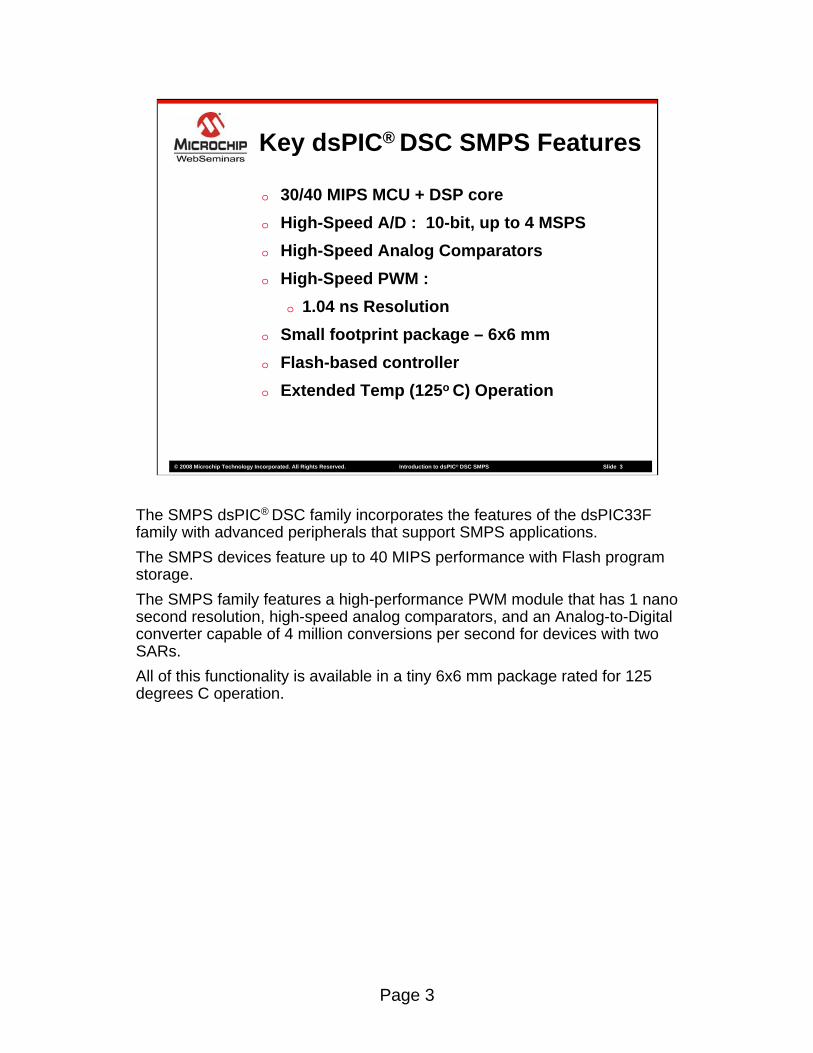
� 30/40 MIPS MCU + DSP core� High-Speed A/D : 10-bit, up to 4 MSPS � High-Speed Analog Comparators� High-Speed PWM :
� 1.04 ns Resolution� Small footprint package – 6x6 mm� Flash-based controller� Extended Temp (125o C) Operation
Key dsPIC® DSC SMPS Features
The SMPS dsPIC® DSC family incorporates the features of the dsPIC33F family with advanced peripherals that support SMPS applications.The SMPS devices feature up to 40 MIPS performance with Flash program storage. The SMPS family features a high-performance PWM module that has 1 nano second resolution, high-speed analog comparators, and an Analog-to-Digital converter capable of 4 million conversions per second for devices with two SARs.All of this functionality is available in a tiny 6x6 mm package rated for 125 degrees C operation.
Page 4
© 2008 Microchip Technology Incorporated. All Rights Reserved. Introduction to dsPIC® DSC SMPS Slide 4
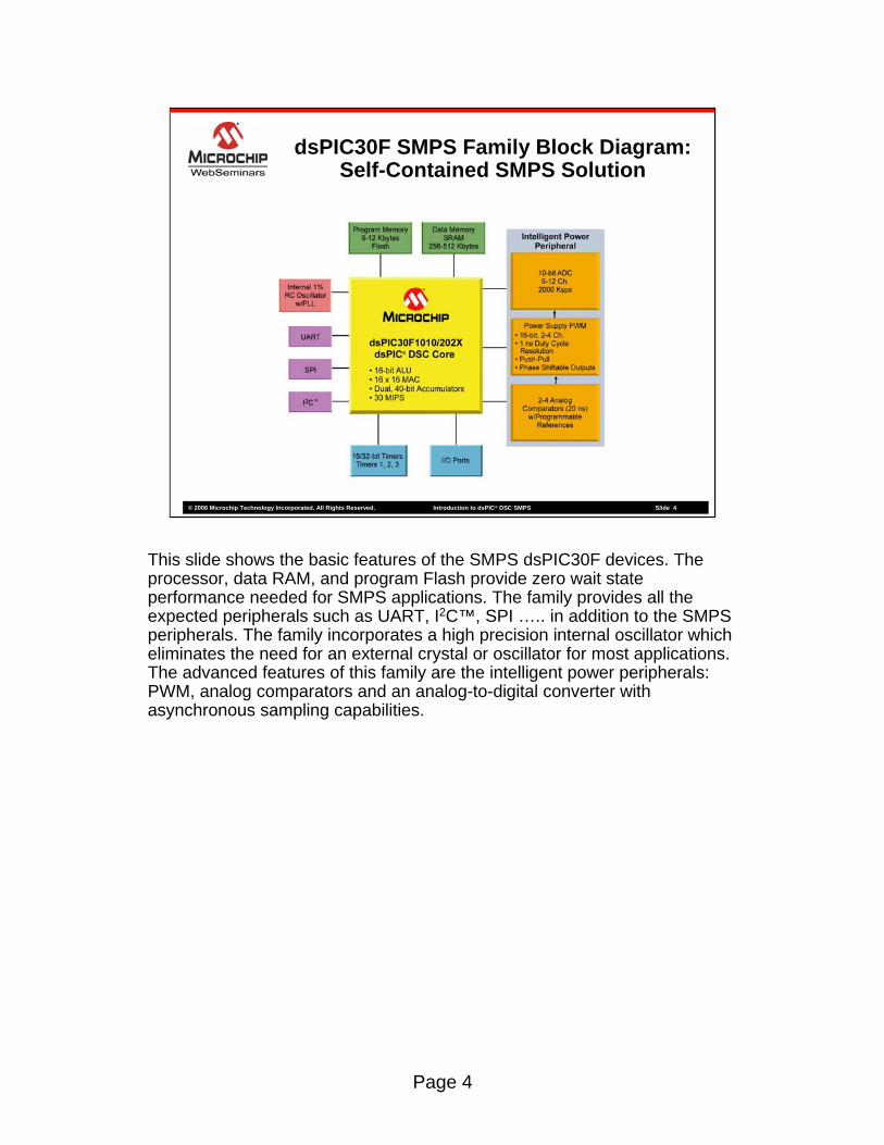
dsPIC30F SMPS Family Block Diagram:Self-Contained SMPS Solution
This slide shows the basic features of the SMPS dsPIC30F devices. The processor, data RAM, and program Flash provide zero wait state performance needed for SMPS applications. The family provides all the expected peripherals such as UART, I2C™, SPI ….. in addition to the SMPS peripherals. The family incorporates a high precision internal oscillator which eliminates the need for an external crystal or oscillator for most applications. The advanced features of this family are the intelligent power peripherals: PWM, analog comparators and an analog-to-digital converter with asynchronous sampling capabilities.
Page 5
© 2008 Microchip Technology Incorporated. All Rights Reserved. Introduction to dsPIC® DSC SMPS Slide 5
dsPIC33F SMPS Family Block Diagram:Self-Contained SMPS Solution
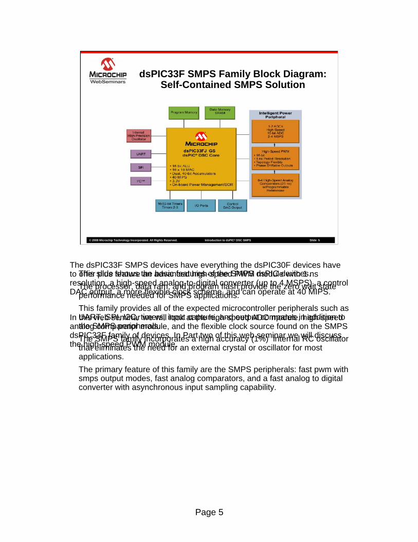
The dsPIC33F SMPS devices have everything the dsPIC30F devices have to offer plus feature an advanced high-speed PWM module with 1 ns resolution, a high-speed analog-to-digital converter (up to 4 MSPS), a control DAC output, a more flexible clock scheme, and can operate at 40 MIPS.
In this web seminar we will look at the high-speed ADC module, high-speed analog comparator module, and the flexible clock source found on the SMPS dsPIC33F family of devices. In Part two of this web seminar we will discuss the high-speed PWM module.
This slide shows the basic features of the SMPS dsPIC devices. The processor, data ram, and program flash provide the zero wait state performance needed for SMPS applications.This family provides all of the expected microcontroller peripherals such as UART, SPI, I2C, timers, input capture, and output compares in addition to the SMPS peripherals.The SMPS family incorporates a high accuracy (1%) internal RC oscillator that eliminates the need for an external crystal or oscillator for most applications.The primary feature of this family are the SMPS peripherals: fast pwm with smps output modes, fast analog comparators, and a fast analog to digital converter with asynchronous input sampling capability.
Page 6
© 2008 Microchip Technology Incorporated. All Rights Reserved. Introduction to dsPIC® DSC SMPS Slide 6
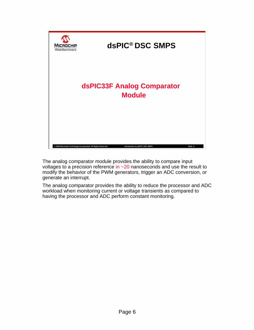
dsPIC33F Analog Comparator Module
dsPIC® DSC SMPS
The analog comparator module provides the ability to compare input voltages to a precision reference in ~20 nanoseconds and use the result to modify the behavior of the PWM generators, trigger an ADC conversion, or generate an interrupt.The analog comparator provides the ability to reduce the processor and ADC workload when monitoring current or voltage transients as compared to having the processor and ADC perform constant monitoring.
Page 7
© 2008 Microchip Technology Incorporated. All Rights Reserved. Introduction to dsPIC® DSC SMPS Slide 7
dsPIC33F High-Speed Comparator Block Diagram
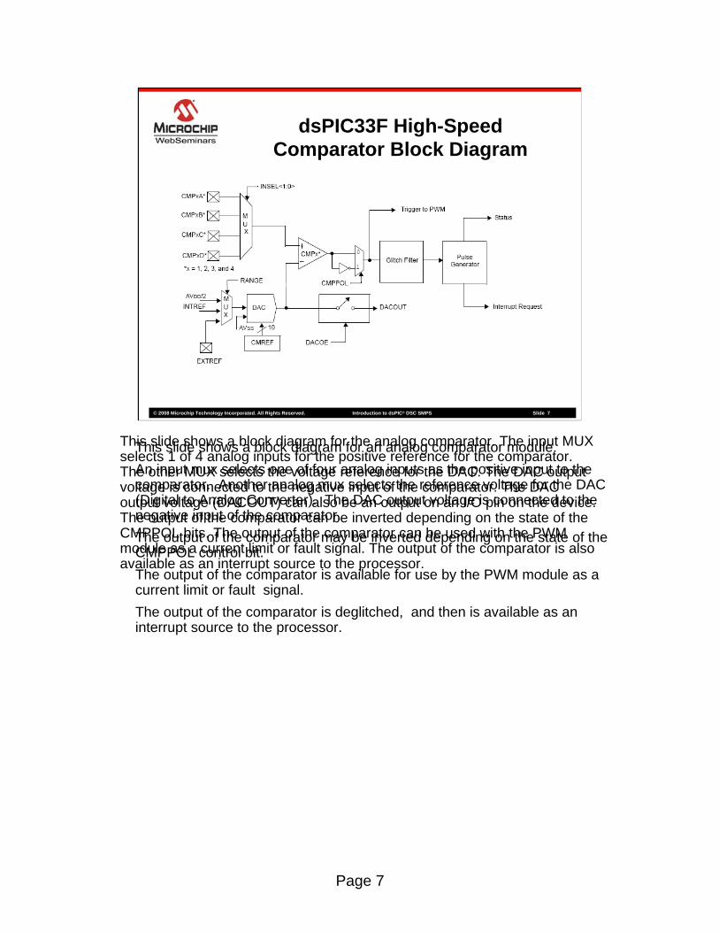
This slide shows a block diagram for the analog comparator. The input MUX selects 1 of 4 analog inputs for the positive reference for the comparator. The other MUX selects the voltage reference for the DAC. The DAC output voltage is connected to the negative input of the comparator. The DAC output voltage (DACOUT) can also be an output on an I/O pin on the device. The output of the comparator can be inverted depending on the state of the CMPPOL bits. The output of the comparator can be used with the PWM module as a current limit or fault signal. The output of the comparator is also available as an interrupt source to the processor.
This slide shows a block diagram for an analog comparator module.An input mux selects one of four analog inputs as the positive input to the comparator. Another analog mux selects the reference voltage for the DAC (Digital to Analog Converter). The DAC output voltage is connected to the negative input of the comparator.The output of the comparator may be inverted depending on the state of the CMPPOL control bit.The output of the comparator is available for use by the PWM module as a current limit or fault signal.The output of the comparator is deglitched, and then is available as an interrupt source to the processor.

Page 8
© 2006 Microchip Technology Incorporated. All Rights Reserved. Introduction to the dsPIC® DSC SMPS Slide 8
� Programmable Reference:� +/-1% Accurate (for a given VDD range)� 0-1.2V Ref or AvDD/2 or external reference� 1024 steps (i.e. 1.2 mv, 2.4 mv, …, 1.2V)� Built in hysterisis to prevent oscillation� Comparator delay: 20 nsec
Analog Comparator
ADC input pin
+
-
On-chip Reference (1.2 V 1%)or AvDD/2 or
external reference (<Avdd-1.6V)
Digital Signalto PWM module
ProgrammableDivider
(1024 steps)
The SMPS dsPIC® DSC has high-speed analog comparators, each with their own programmable references. The reference DACs have 10-bit resolution, and the ability to select internal or external voltage references.The voltage to the reference DACs may come from the analog power supply pin (Avdd/2), an internal 1.2 V reference, or an external pin.The comparators are high speed and can shut down the PWM outputsimmediately (asynchronously to any system clocks).
Page 9
© 2008 Microchip Technology Incorporated. All Rights Reserved. Introduction to dsPIC® DSC SMPS Slide 9
Analog Comparator
� Each analog comparator has two control registers:
bit7 6 5 4 3 2 1 bit0
bit15 14 13 12 11 10 9 bit8
CMPCONx Register
bit7 6 5 4 3 2 1 bit0CMREF<7:0>
bit15 14 13 12 11 10 9 bit8
CMPDACx Register
DACOE----CMPSIDL-CMPON
RANGECMPPOL-CMPSTATINSEL<1:0>
CMPEF<9:8>------
-EXTREF
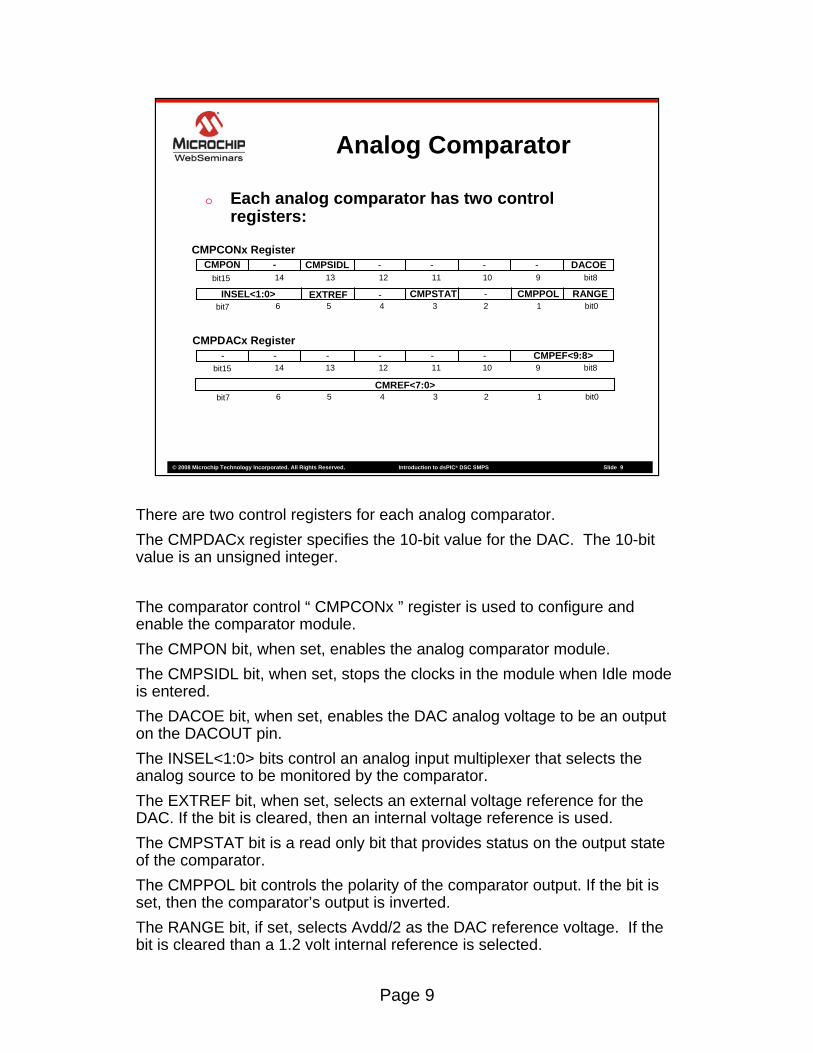
There are two control registers for each analog comparator.The CMPDACx register specifies the 10-bit value for the DAC. The 10-bit value is an unsigned integer.
The comparator control “ CMPCONx ” register is used to configure and enable the comparator module. The CMPON bit, when set, enables the analog comparator module.The CMPSIDL bit, when set, stops the clocks in the module when Idle mode is entered.The DACOE bit, when set, enables the DAC analog voltage to be an output on the DACOUT pin. The INSEL<1:0> bits control an analog input multiplexer that selects the analog source to be monitored by the comparator.The EXTREF bit, when set, selects an external voltage reference for the DAC. If the bit is cleared, then an internal voltage reference is used.The CMPSTAT bit is a read only bit that provides status on the output state of the comparator.The CMPPOL bit controls the polarity of the comparator output. If the bit is set, then the comparator’s output is inverted.The RANGE bit, if set, selects Avdd/2 as the DAC reference voltage. If the bit is cleared than a 1.2 volt internal reference is selected.
Page 10
© 2008 Microchip Technology Incorporated. All Rights Reserved. Introduction to dsPIC® DSC SMPS Slide 10
dsPIC33F ADC Module
dsPIC® DSC SMPS
The Analog-to-Digital Converter module for the SMPS family has features uniquely suited to support SMPS applications.

Page 11
© 2008 Microchip Technology Incorporated. All Rights Reserved. Introduction to dsPIC® DSC SMPS Slide 11
SMPS 10-bit A/D Converter� 10-bit resolution, high accuracy� Up to 4 Million Samples per Second conversion rate � 6 to 12 input channels (or higher(1))� Up to two internal analog inputs� Dedicated result registers for each analog input � Analog input range: 0 to 3.3V� Low latency improves control loop stability� Advanced Sampling Capability:
� Individual triggers for each S&H� Samples may be simultaneous� Samples may be uniquely timed� Sample acquisitions are precisely timed
(1) Future devices may have more analog input channels
The SMPS Analog-to-Digital Converter has 10-bit resolution and supports up to 4 million sample and convert operations per second (4 MSPS for devices with two SARs).Depending on the SMPS device and package, six to twelve analog inputs per ADC are available and up to two internal analog inputs. Each of the analog inputs has its own dedicated result register.The analog input voltage range is from 0 to 3.3 volts when using a 3.3 volt power supply. For dsPIC30F SMPS devices, the analog input voltage range is from 0 to 5 volts.Each pair of analog inputs (AN0-1, AN2-3, AN4-5, etc…) has unique trigger signals to initiate the sample and convert process.The timing of any input pair’s sample and conversion may be asynchronous to the other inputs.
Page 12
© 2008 Microchip Technology Incorporated. All Rights Reserved. Introduction to dsPIC® DSC SMPS Slide 12
ADC Block Diagram
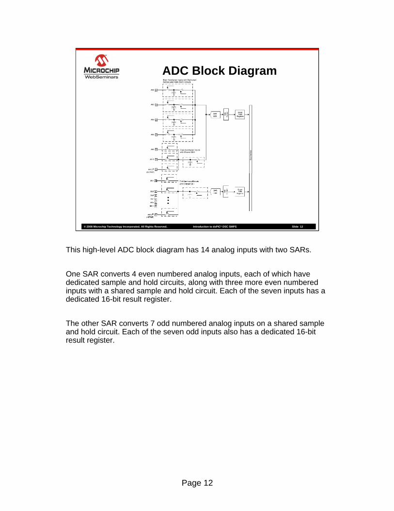
This high-level ADC block diagram has 14 analog inputs with two SARs.
One SAR converts 4 even numbered analog inputs, each of which have dedicated sample and hold circuits, along with three more even numbered inputs with a shared sample and hold circuit. Each of the seven inputs has a dedicated 16-bit result register.
The other SAR converts 7 odd numbered analog inputs on a shared sample and hold circuit. Each of the seven odd inputs also has a dedicated 16-bit result register.

Page 13
© 2008 Microchip Technology Incorporated. All Rights Reserved. Introduction to dsPIC® DSC SMPS Slide 13
Unique SMPS ADC Capability
� Conventional ADCs sample and convert inputs one at a time, or in a fixed sequence. Limited triggering capabilities make it difficult to capture data from independent events.
� The SMPS ADC samples and converts inputs independently, and asynchronously of each other. Data capture from time critical events is simplified with sophisticated triggering capabilities.
Existing ADCs were designed for data logging applications, where a number of conversions are obtained and then processed in “batch”. Most ADCs can either convert a single input or process a sequence of conversions and dump the results into a buffer.SMPS applications have an extremely tight time constraint. The time from when a sample of an analog signal is taken to the time the control loop can update and output a new PWM value in response to that sample is called “Latency”. The latency determines the overall frequency of the control loop, it affects the stability of the control loop, and it directly affects the performance of the SMPS application.If a processor is supporting multiple control loops for multiple outputs that are operating at different frequencies, a standardized sampling sequence can not provide optimal sample to output latencies.To reduce system cost, it is desirable to measure currents at circuit locations that do not have high common mode voltages. Often, these accessible current sense locations offer valid current sensing only during transistor “on”times.The SMPS ADC is capable of sampling critical inputs at independent times relative to other inputs.
Page 14
© 2008 Microchip Technology Incorporated. All Rights Reserved. Introduction to dsPIC® DSC SMPS Slide 14
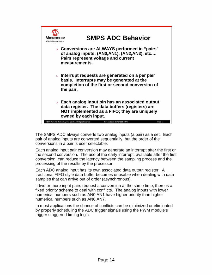
SMPS ADC Behavior� Conversions are ALWAYS performed in “pairs”
of analog inputs: (AN0,AN1), (AN2,AN3), etc.…Pairs represent voltage and current measurements.
� Interrupt requests are generated on a per pair basis. Interrupts may be generated at the completion of the first or second conversion of the pair.
� Each analog input pin has an associated output data register. The data buffers (registers) are NOT implemented as a FIFO; they are uniquely owned by each input.
The SMPS ADC always converts two analog inputs (a pair) as a set. Each pair of analog inputs are converted sequentially, but the order of the conversions in a pair is user selectable.Each analog input pair conversion may generate an interrupt after the first or the second conversion. The use of the early interrupt, available after the first conversion, can reduce the latency between the sampling process and the processing of the results by the processor.Each ADC analog input has its own associated data output register. A traditional FIFO style data buffer becomes unusable when dealing with data samples that can arrive out of order (asynchronous).If two or more input pairs request a conversion at the same time, there is a fixed priority scheme to deal with conflicts. The analog inputs with lower numerical numbers such as AN0,AN1 have higher priority than higher numerical numbers such as AN6,AN7.In most applications the chance of conflicts can be minimized or eliminated by properly scheduling the ADC trigger signals using the PWM module’s trigger staggered timing logic.
Page 15
© 2008 Microchip Technology Incorporated. All Rights Reserved. Introduction to dsPIC® DSC SMPS Slide 15
SMPS ADC
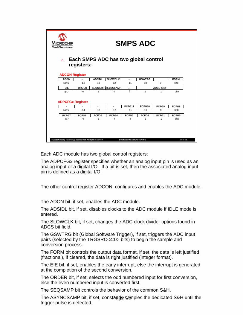
� Each SMPS ADC has two global control registers:
bit7 6 5 4 3 2 1 bit0
bit15 14 13 12 11 10 9 bit8
ADCON Register
bit7 6 5 4 3 2 1 bit0
bit15 14 13 12 11 10 9 bit8
ADPCFGx Register
FORMGSWTRG-SLOWCLKADSIDL-ADON
ADCS<2:0>SEQSAMPORDEREIE
PCFG10PCFG11---- PCFG9 PCFG8
PCFG2PCFG3PCFG4PCFG5PCFG6PCFG7 PCFG1 PCFG0
-ASYNCSAMP
Each ADC module has two global control registers:The ADPCFGx register specifies whether an analog input pin is used as an analog input or a digital I/O. If a bit is set, then the associated analog input pin is defined as a digital I/O.
The other control register ADCON, configures and enables the ADC module.
The ADON bit, if set, enables the ADC module.The ADSIDL bit, if set, disables clocks to the ADC module if IDLE mode is entered.The SLOWCLK bit, if set, changes the ADC clock divider options found in ADCS bit field.The GSWTRG bit (Global Software Trigger), if set, triggers the ADC input pairs (selected by the TRGSRC<4:0> bits) to begin the sample andconversion process.The FORM bit controls the output data format, if set, the data is left justified (fractional), if cleared, the data is right justified (integer format).The EIE bit, if set, enables the early interrupt, else the interrupt is generated at the completion of the second conversion.The ORDER bit, if set, selects the odd numbered input for first conversion, else the even numbered input is converted first.The SEQSAMP bit controls the behavior of the common S&H.The ASYNCSAMP bit, if set, constantly samples the dedicated S&H until the trigger pulse is detected.
Page 16
© 2008 Microchip Technology Incorporated. All Rights Reserved. Introduction to dsPIC® DSC SMPS Slide 16
SMPS ADC
� Each SMPS ADC has a global status register:
bit7 6 5 4 3 2 1 bit0
bit15 14 13 12 11 10 9 bit8
ADSTAT Register
P2RDYP3RDYP4RDYP5RDYP6RDY- P1RDY P0RDY
----- - --
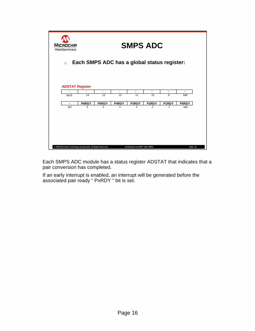
Each SMPS ADC module has a status register ADSTAT that indicates that a pair conversion has completed. If an early interrupt is enabled, an interrupt will be generated before the associated pair ready “ PxRDY ” bit is set.
Page 17
© 2008 Microchip Technology Incorporated. All Rights Reserved. Introduction to dsPIC® DSC SMPS Slide 17
SMPS ADC
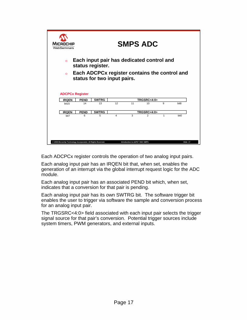
� Each input pair has dedicated control and status register.
� Each ADCPCx register contains the control and status for two input pairs.
bit7 6 5 4 3 2 1 bit0
bit15 14 13 12 11 10 9 bit8
ADCPCx RegisterSWTRGPENDIRQEN TRGSRC<4:0>
SWTRGPENDIRQEN TRGSRC<4:0>
Each ADCPCx register controls the operation of two analog input pairs.Each analog input pair has an IRQEN bit that, when set, enables the generation of an interrupt via the global interrupt request logic for the ADC module.Each analog input pair has an associated PEND bit which, when set, indicates that a conversion for that pair is pending.Each analog input pair has its own SWTRG bit. The software trigger bit enables the user to trigger via software the sample and conversion process for an analog input pair.The TRGSRC<4:0> field associated with each input pair selects the trigger signal source for that pair’s conversion. Potential trigger sources include system timers, PWM generators, and external inputs.
Page 18
© 2006 Microchip Technology Incorporated. All Rights Reserved. Introduction to the dsPIC® DSC SMPS Slide 18
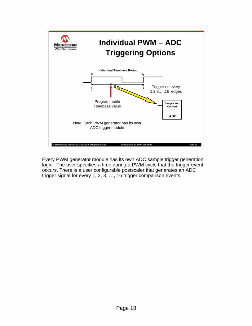
Individual PWM – ADC Triggering Options
Individual Timebase Period
Trigger on every 1,2,3,…,16 edges
Programmable Timebase value
x
ADC
Sample and Convert
Note: Each PWM generator has its own ADC trigger module
Every PWM generator module has its own ADC sample trigger generation logic. The user specifies a time during a PWM cycle that the trigger event occurs. There is a user configurable postscaler that generates an ADC trigger signal for every 1, 2, 3, …, 16 trigger comparison events.
Page 19
© 2006 Microchip Technology Incorporated. All Rights Reserved. Introduction to the dsPIC® DSC SMPS Slide 19
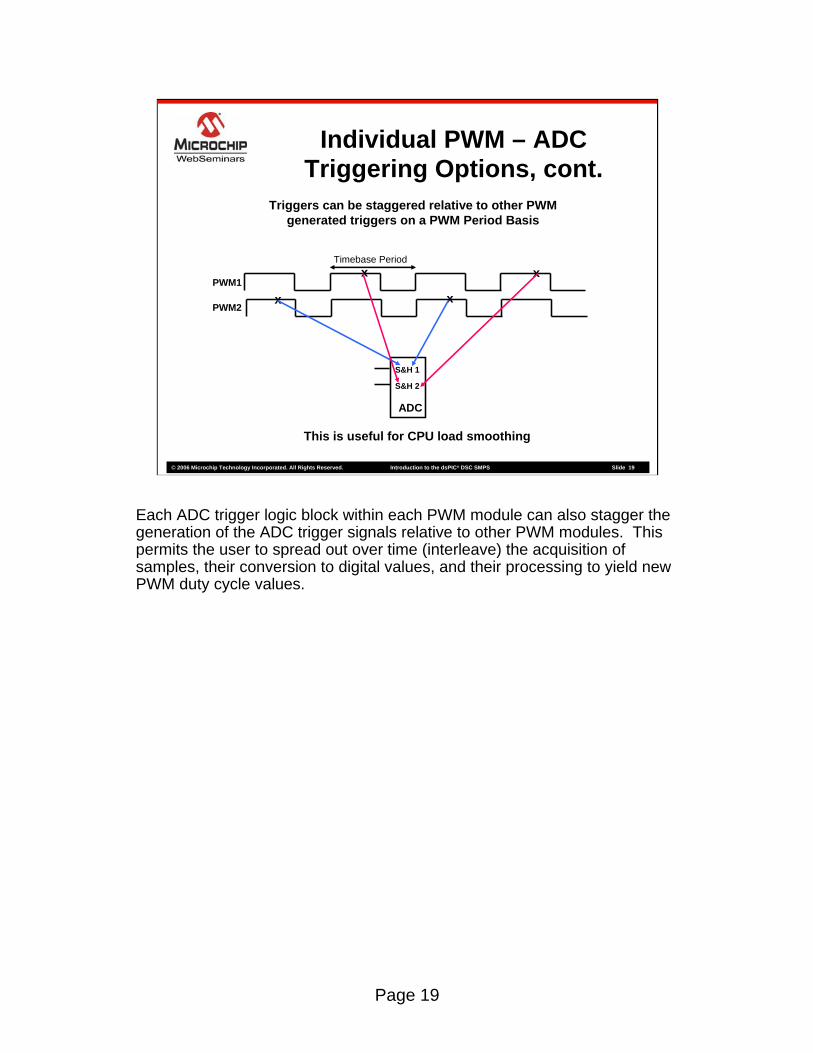
Individual PWM – ADC Triggering Options, cont.
Timebase Periodx
ADC
S&H 1
Triggers can be staggered relative to other PWM generated triggers on a PWM Period Basis
x
x
xPWM1
PWM2
S&H 2
This is useful for CPU load smoothing
Each ADC trigger logic block within each PWM module can also stagger the generation of the ADC trigger signals relative to other PWM modules. This permits the user to spread out over time (interleave) the acquisition of samples, their conversion to digital values, and their processing to yield new PWM duty cycle values.

Page 20
© 2008 Microchip Technology Incorporated. All Rights Reserved. Introduction to dsPIC® DSC SMPS Slide 20
SMPS ADC
� Each SMPS ADC has a Base register.� The Base register, when read, provides the
sum of the user defined base address plus an offset representing the pending interrupt with the highest priority.
� The ADBASEx register provides the user a means to quickly process interrupts from multiple input pairs.
bit7 6 5 4 3 2 1 bit0
bit15 14 13 12 11 10 9 bit8
ADBASE Register
ADBASE<7:1>
ADBASE<15:8>
-
The ADBASE register contains the base address of the user’s ADC Interrupt Service Routine jump table. This register, when read, contains the sum of the ADBASE register contents and the encoded value of the PxRDY status bits. The ADBASE register enables the user to use a single global interrupt from the ADC and yet process the interrupts as if they were provided individual interrupt vectors. The user in the ISR (interrupt Service Routine) reads the ADBASE register and copies it into a W register. The user then performs an indirect jump (GOTO) through the W register to a jump table. The jump table enables each ADC interrupt to be processed separately with unique software if required by an application.
The USER does not have to use the ADBASE register feature but, in some applications, it can save a lot of time that would be spent examining interrupt status bits in the ADSTATx register to determine which input pair interrupt is to be processed.
Page 21
© 2008 Microchip Technology Incorporated. All Rights Reserved. Introduction to dsPIC® DSC SMPS Slide 21
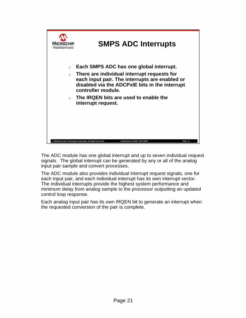
SMPS ADC Interrupts
� Each SMPS ADC has one global interrupt.� There are individual interrupt requests for
each input pair. The interrupts are enabled or disabled via the ADCPxIE bits in the interrupt controller module.
� The IRQEN bits are used to enable the interrupt request.
The ADC module has one global interrupt and up to seven individual request signals. The global interrupt can be generated by any or all of the analog input pair sample and convert processes. The ADC module also provides individual interrupt request signals, one for each input pair, and each individual interrupt has its own interrupt vector. The individual interrupts provide the highest system performance and minimum delay from analog sample to the processor outputting an updated control loop response.Each analog input pair has its own IRQEN bit to generate an interrupt when the requested conversion of the pair is complete.
Page 22
© 2008 Microchip Technology Incorporated. All Rights Reserved. Introduction to dsPIC® DSC SMPS Slide 22
dsPIC33F System Clock Module
dsPIC® DSC SMPS
The system clock module enables the user to specify the system clock source and the system frequency of operation.
Page 23
© 2008 Microchip Technology Incorporated. All Rights Reserved. Introduction to dsPIC® DSC SMPS Slide 23
Clocking Options
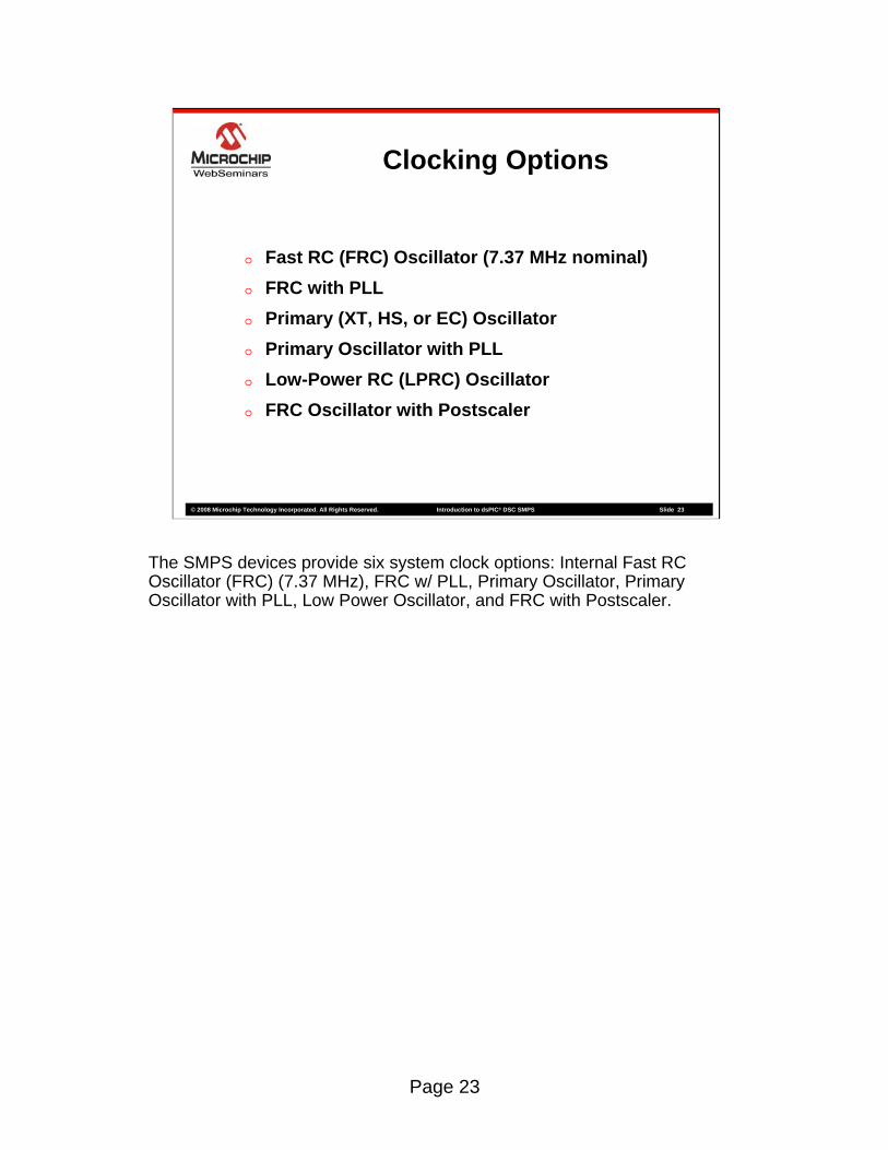
� Fast RC (FRC) Oscillator (7.37 MHz nominal)� FRC with PLL� Primary (XT, HS, or EC) Oscillator� Primary Oscillator with PLL� Low-Power RC (LPRC) Oscillator� FRC Oscillator with Postscaler
The SMPS devices provide six system clock options: Internal Fast RC Oscillator (FRC) (7.37 MHz), FRC w/ PLL, Primary Oscillator, Primary Oscillator with PLL, Low Power Oscillator, and FRC with Postscaler.
Page 24
© 2008 Microchip Technology Incorporated. All Rights Reserved. Introduction to dsPIC® DSC SMPS Slide 24
Clocking Options
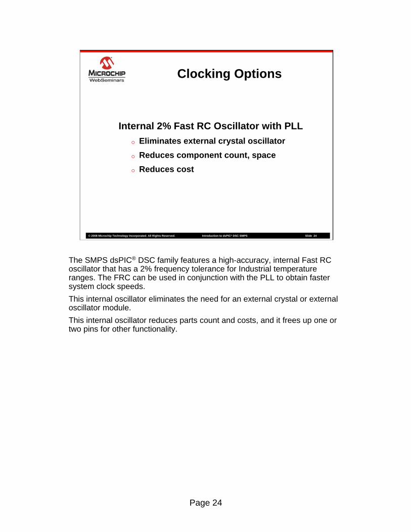
Internal 2% Fast RC Oscillator with PLL� Eliminates external crystal oscillator � Reduces component count, space� Reduces cost
The SMPS dsPIC® DSC family features a high-accuracy, internal Fast RC oscillator that has a 2% frequency tolerance for Industrial temperature ranges. The FRC can be used in conjunction with the PLL to obtain faster system clock speeds.This internal oscillator eliminates the need for an external crystal or external oscillator module.This internal oscillator reduces parts count and costs, and it frees up one or two pins for other functionality.
Page 25
© 2008 Microchip Technology Incorporated. All Rights Reserved. Introduction to dsPIC® DSC SMPS Slide 25
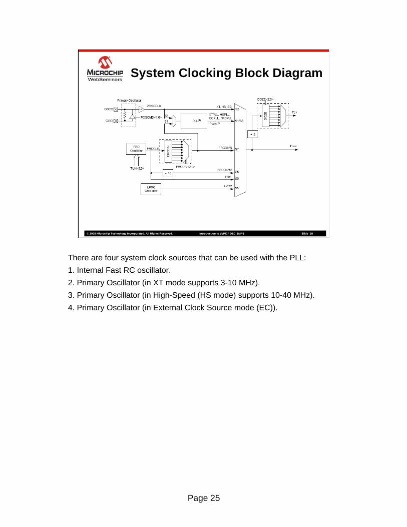
System Clocking Block Diagram
There are four system clock sources that can be used with the PLL:1. Internal Fast RC oscillator.2. Primary Oscillator (in XT mode supports 3-10 MHz).3. Primary Oscillator (in High-Speed (HS mode) supports 10-40 MHz).4. Primary Oscillator (in External Clock Source mode (EC)).
Page 26
© 2008 Microchip Technology Incorporated. All Rights Reserved. Introduction to dsPIC® DSC SMPS Slide 26
System Clocking Block Diagram Cont.
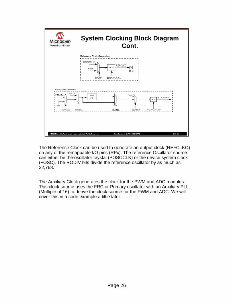
The Reference Clock can be used to generate an output clock (REFCLKO) on any of the remappable I/O pins (RPx). The reference Oscillator source can either be the oscillator crystal (POSCCLK) or the device system clock (FOSC). The RODIV bits divide the reference oscillator by as much as 32,768.
The Auxiliary Clock generates the clock for the PWM and ADC modules. This clock source uses the FRC or Primary oscillator with an Auxiliary PLL (Multiple of 16) to derive the clock source for the PWM and ADC. We will cover this in a code example a little later.
Page 27
© 2008 Microchip Technology Incorporated. All Rights Reserved. Introduction to dsPIC® DSC SMPS Slide 27
SMPS System Clock Module
� The OSCCON register controls the selection of the system clock.
bit7 6 5 4 3 2 1 bit0
bit15 14 13 12 11 10 9 bit8
OSCCON RegisterNOSC<2:0>- -
IOLOCK OSWEN-
COSC<2:0>
- -CFLOCKCLKLOCK
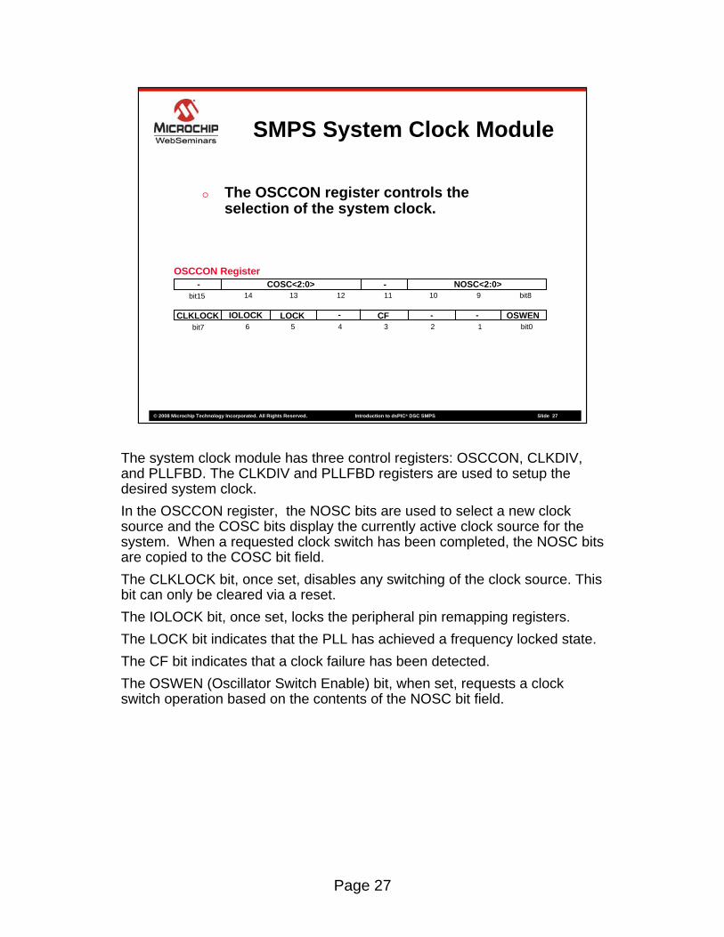
The system clock module has three control registers: OSCCON, CLKDIV, and PLLFBD. The CLKDIV and PLLFBD registers are used to setup the desired system clock. In the OSCCON register, the NOSC bits are used to select a new clock source and the COSC bits display the currently active clock source for the system. When a requested clock switch has been completed, the NOSC bits are copied to the COSC bit field.The CLKLOCK bit, once set, disables any switching of the clock source. This bit can only be cleared via a reset.The IOLOCK bit, once set, locks the peripheral pin remapping registers.The LOCK bit indicates that the PLL has achieved a frequency locked state.The CF bit indicates that a clock failure has been detected.The OSWEN (Oscillator Switch Enable) bit, when set, requests a clock switch operation based on the contents of the NOSC bit field.
Page 28
© 2008 Microchip Technology Incorporated. All Rights Reserved. Introduction to dsPIC® DSC SMPS Slide 28
SMPS System Clock Module
bit7 6 5 4 3 2 1 bit0
bit15 14 13 12 11 10 9 bit8
ACLKCON RegisterAPSTSCLR<2:0>ENAPLL -
FRCSEL --- ---ASRCSEL
APLLCK SELACLK -
� The ACLKCON register configures the input clock for the PWM and ADC module.
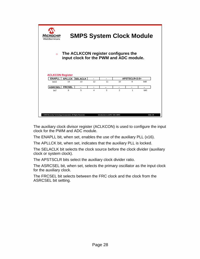
The auxiliary clock divisor register (ACLKCON) is used to configure the input clock for the PWM and ADC module. The ENAPLL bit, when set, enables the use of the auxiliary PLL (x16).The APLLCK bit, when set, indicates that the auxiliary PLL is locked.The SELACLK bit selects the clock source before the clock divider (auxiliary clock or system clock).The APSTSCLR bits select the auxiliary clock divider ratio.The ASRCSEL bit, when set, selects the primary oscillator as the input clock for the auxiliary clock.The FRCSEL bit selects between the FRC clock and the clock from the ASRCSEL bit setting.
Page 29
© 2008 Microchip Technology Incorporated. All Rights Reserved. Introduction to dsPIC® DSC SMPS Slide 29
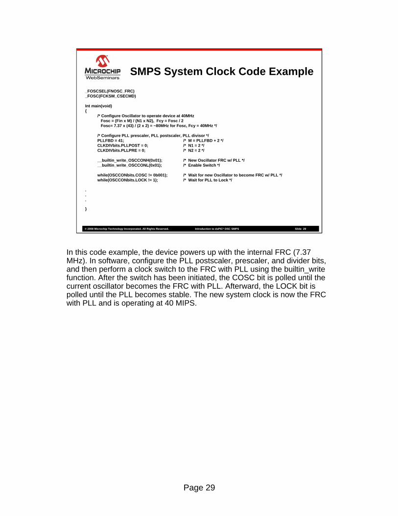
SMPS System Clock Code Example_FOSCSEL(FNOSC_FRC)_FOSC(FCKSM_CSECMD)
Int main(void){
/* Configure Oscillator to operate device at 40MHzFosc = (Fin x M) / (N1 x N2), Fcy = Fosc / 2Fosc= 7.37 x (43) / (2 x 2) = ~80MHz for Fosc, Fcy = 40MHz */
/* Configure PLL prescaler, PLL postscaler, PLL divisor */PLLFBD = 41; /* M = PLLFBD + 2 */CLKDIVbits.PLLPOST = 0; /* N1 = 2 */CLKDIVbits.PLLPRE = 0; /* N2 = 2 */
__builtin_write_OSCCONH(0x01); /* New Oscillator FRC w/ PLL */__builtin_write_OSCCONL(0x01); /* Enable Switch */
while(OSCCONbits.COSC != 0b001); /* Wait for new Oscillator to become FRC w/ PLL */ while(OSCCONbits.LOCK != 1); /* Wait for PLL to Lock */
.
.
.
}
In this code example, the device powers up with the internal FRC (7.37 MHz). In software, configure the PLL postscaler, prescaler, and divider bits, and then perform a clock switch to the FRC with PLL using the builtin_write function. After the switch has been initiated, the COSC bit is polled until the current oscillator becomes the FRC with PLL. Afterward, the LOCK bit is polled until the PLL becomes stable. The new system clock is now the FRC with PLL and is operating at 40 MIPS.
Page 30
© 2008 Microchip Technology Incorporated. All Rights Reserved. Introduction to dsPIC® DSC SMPS Slide 30
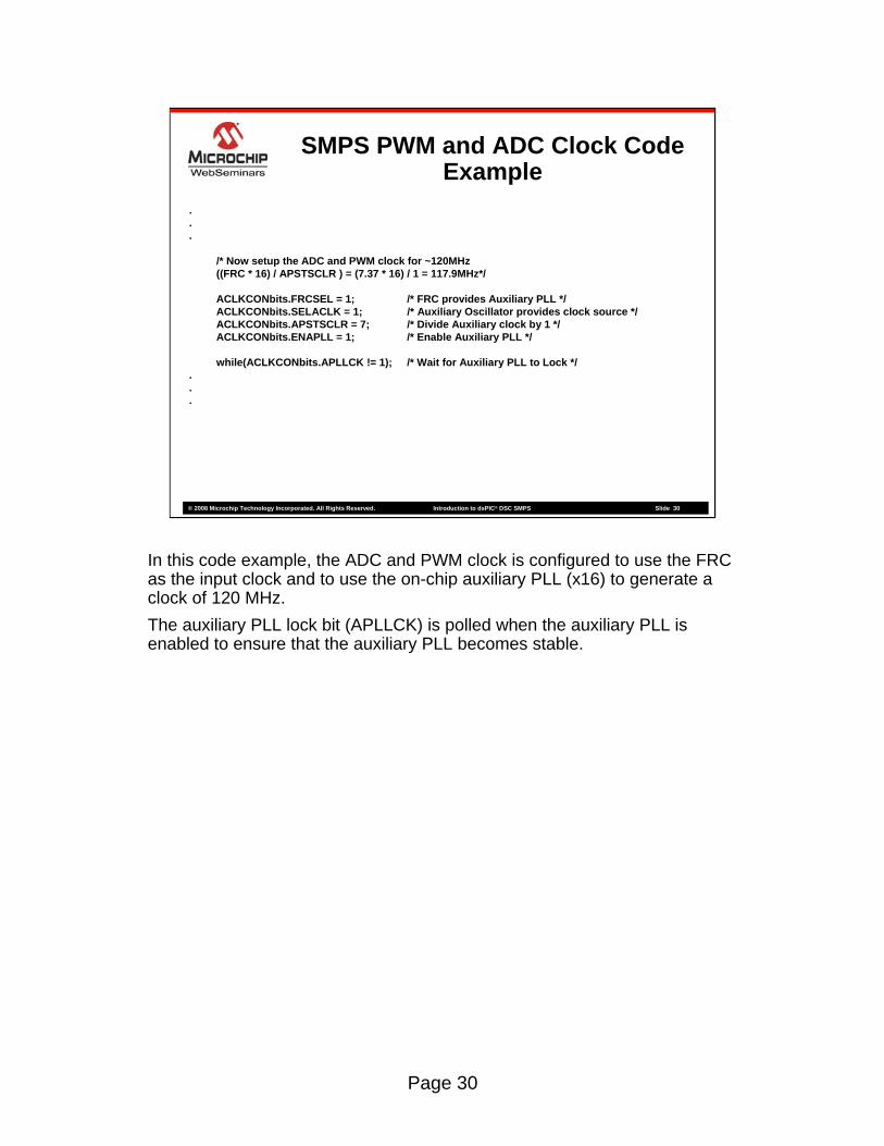
SMPS PWM and ADC Clock Code Example
.
.
.
/* Now setup the ADC and PWM clock for ~120MHz((FRC * 16) / APSTSCLR ) = (7.37 * 16) / 1 = 117.9MHz*/
ACLKCONbits.FRCSEL = 1; /* FRC provides Auxiliary PLL */ACLKCONbits.SELACLK = 1; /* Auxiliary Oscillator provides clock source */ACLKCONbits.APSTSCLR = 7; /* Divide Auxiliary clock by 1 */ACLKCONbits.ENAPLL = 1; /* Enable Auxiliary PLL */
while(ACLKCONbits.APLLCK != 1); /* Wait for Auxiliary PLL to Lock */...
In this code example, the ADC and PWM clock is configured to use the FRC as the input clock and to use the on-chip auxiliary PLL (x16) to generate a clock of 120 MHz.The auxiliary PLL lock bit (APLLCK) is polled when the auxiliary PLL is enabled to ensure that the auxiliary PLL becomes stable.
Page 31
© 2008 Microchip Technology Incorporated. All Rights Reserved. Introduction to dsPIC® DSC SMPS Slide 31
Key Support Documents
Microchip Web Sites: www.microchip.com/smpswww.microchip.com/16-bit
For device data sheets, Family Reference Manuals, and other related documents please visit the following Microchip websites.

Page 32
© 2008 Microchip Technology Incorporated. All Rights Reserved. Introduction to dsPIC® DSC SMPS Slide 32
Thank You
Thank you for attending this Webinar
Page 33
© 2008 Microchip Technology Incorporated. All Rights Reserved. Introduction to dsPIC® DSC SMPS Slide 33
Trademarks
� The Microchip name and logo, the Microchip logo, Accuron, dsPIC, KeeLoq, KeeLoq logo, MPLAB, PIC, PICmicro, PICSTART, rfPIC, SmartShunt and UNI/O are registered trademarks of Microchip Technology Incorporated in the U.S.A. and other countries.
� FilterLab, Linear Active Thermistor, MXDEV, MXLAB, SEEVAL, SmartSensorand The Embedded Control Solutions Company are registered trademarks of Microchip Technology Incorporated in the U.S.A.
� Analog-for-the-Digital Age, Application Maestro, CodeGuard, dsPICDEM, dsPICDEM.net, dsPICworks, dsSPEAK, ECAN, ECONOMONITOR, FanSense, In-Circuit Serial Programming, ICSP, ICEPIC, Mindi, MiWi, MPASM, MPLAB Certified logo, MPLIB, MPLINK, mTouch, PICkit, PICDEM, PICDEM.net, PICtail, PIC32 logo, PowerCal, PowerInfo, PowerMate, PowerTool, REAL ICE, rfLAB, Select Mode, Total Endurance, WiperLock and ZENA are trademarks of Microchip Technology Incorporated in the U.S.A. and other countries.
� SQTP is a service mark of Microchip Technology Incorporated in the U.S.A.� All other trademarks mentioned herein are property of their respective
companies.� © 2008, Microchip Technology Incorporated, All Rights Reserved.