introduction to · 2013-07-23 · 4.6 assignment statements 51 4.7 vhdl data types 51 4.8 vhdl...
TRANSCRIPT


INTRODUCTION TODIGITAL SYSTEMS

INTRODUCTION TODIGITAL SYSTEMS
Modeling, Synthesis, and SimulationUsing VHDL
Mohammed FerdjallahThe Virginia Modeling, Analysis and Simulation Center
Old Dominion University
Suffolk, Virginia
and ECPI College of Technology

Copyright � 2011 by John Wiley & Sons, Inc. All rights reserved.
Published by John Wiley & Sons, Inc., Hoboken, New Jersey.
Published simultaneously in Canada.
No part of this publication may be reproduced, stored in a retrieval system, or transmitted in any form
or by any means, electronic, mechanical, photocopying, recording, scanning, or otherwise, except as
permitted under Sections 107 or 108 of the 1976 United States Copyright Act, without either the
prior written permission of the Publisher, or authorization through payment of the appropriate per-copy
fee to the Copyright Clearance Center, Inc., 222 Rosewood Drive, Danvers, MA 01923, (978) 750-8400,
fax (978) 750-4470, or on the web at www.copyright.com. Requests to the Publisher for permission should
be addressed to the Permissions Department, John Wiley & Sons, Inc., 111 River Street, Hoboken,
NJ 07030, (201) 748-6011, fax (201) 748-6008, or online at http://www.wiley.com/go/permission.
Limit of Liability/Disclaimer of Warranty: While the publisher and author have used their best efforts
in preparing this book, they make no representations or warranties with respect to the accuracy or
completeness of the contents of this book and specifically disclaim any implied warranties of
merchantability or fitness for a particular purpose. No warranty may be created or extended by sales
representatives or written sales materials. The advice and strategies contained herein may not be suitable
for your situation. You should consult with a professional where appropriate. Neither the publisher nor
author shall be liable for any loss of profit or any other commercial damages, including but not limited
to special, incidental, consequential, or other damages.
For general information on our other products and services or for technical support, please contact
our Customer Care Department within the United States at (800) 762-2974, outside the United States
at (317) 572-3993 or fax (317) 572-4002.
Wiley also publishes its books in a variety of electronic formats. Some content that appears in print may
not be available in electronic formats. For more information about Wiley products, visit our web site
at www.wiley.com.
Library of Congress Cataloging-in-Publication Data:
Ferdjallah, Mohammed.
Introduction to digital systems : modeling, synthesis, and simulation using VHDL / Mohammed
Ferdjallah.
p. cm.
Includes bibliographical references and index.
ISBN 978-0-470-90055-0 (cloth)
1. Digital electronics. 2. Digital electronics–Computer simulation. 3. VHDL (Computer
hardware description language) I. Title.
TK7868.D5F47 2011
621.39’2–dc22 2010041036
Printed in the United States of America
oBooK ISBN: 9781118007716
ePDF ISBN: 9781118007693
ePub ISBN: 9781118007709
10 9 8 7 6 5 4 3 2 1
CONTENTS
Preface ix
1 Digital System Modeling and Simulation 1
1.1 Objectives 1
1.2 Modeling, Synthesis, and Simulation Design 1
1.3 History of Digital Systems 2
1.4 Standard Logic Devices 2
1.5 Custom-Designed Logic Devices 3
1.6 Programmable Logic Devices 3
1.7 Simple Programmable Logic Devices 4
1.8 Complex Programmable Logic Devices 5
1.9 Field-Programmable Gate Arrays 6
1.10 Future of Digital Systems 7
Problems 8
2 Number Systems 9
2.1 Objectives 9
2.2 Bases and Number Systems 9
2.3 Number Conversions 11
2.4 Data Organization 13
2.5 Signed and Unsigned Numbers 13
2.6 Binary Arithmetic 16
2.7 Addition of Signed Numbers 17
2.8 Binary-Coded Decimal Representation 19
2.9 BCD Addition 20
Problems 21
3 Boolean Algebra and Logic 24
3.1 Objectives 24
3.2 Boolean Theory 24
3.3 Logic Variables and Logic Functions 25
3.4 Boolean Axioms and Theorems 25
3.5 Basic Logic Gates and Truth Tables 27
3.6 Logic Representations and Circuit Design 27
v
3.7 Truth Table 28
3.8 Timing Diagram 31
3.9 Logic Design Concepts 31
3.10 Sum-of-Products Design 32
3.11 Product-of-Sums Design 33
3.12 Design Examples 34
3.13 NAND and NOR Equivalent Circuit Design 36
3.14 Standard Logic Integrated Circuits 37
Problems 39
4 VHDL Design Concepts 46
4.1 Objectives 46
4.2 CAD Tool–Based Logic Design 46
4.3 Hardware Description Languages 47
4.4 VHDL Language 48
4.5 VHDL Programming Structure 48
4.6 Assignment Statements 51
4.7 VHDL Data Types 51
4.8 VHDL Operators 55
4.9 VHDL Signal and Generate Statements 56
4.10 Sequential Statements 58
4.11 Loops and Decision-Making Statements 59
4.12 Subcircuit Design 61
4.13 Packages and Components 61
Problems 64
5 Integrated Logic 68
5.1 Objectives 68
5.2 Logic Signals 68
5.3 Logic Switches 69
5.4 NMOS and PMOS Logic Gates 70
5.5 CMOS Logic Gates 72
5.6 CMOS Logic Networks 75
5.7 Practical Aspects of Logic Gates 76
5.8 Transmission Gates 79
Problems 81
6 Logic Function Optimization 87
6.1 Objectives 87
6.2 Logic Function Optimization Process 87
6.3 Karnaugh Maps 87
6.4 Two-Variable Karnaugh Map 89
6.5 Three-Variable Karnaugh Map 90
vi CONTENTS
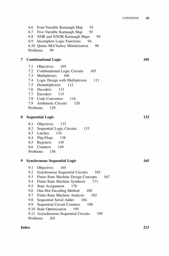
6.6 Four-Variable Karnaugh Map 91
6.7 Five-Variable Karnaugh Map 93
6.8 XOR and NXOR Karnaugh Maps 94
6.9 Incomplete Logic Functions 94
6.10 Quine–McCluskey Minimization 96
Problems 99
7 Combinational Logic 105
7.1 Objectives 105
7.2 Combinational Logic Circuits 105
7.3 Multiplexers 106
7.4 Logic Design with Multiplexers 111
7.5 Demultiplexers 112
7.6 Decoders 113
7.7 Encoders 115
7.8 Code Converters 116
7.9 Arithmetic Circuits 120
Problems 129
8 Sequential Logic 133
8.1 Objectives 133
8.2 Sequential Logic Circuits 133
8.3 Latches 134
8.4 Flip-Flops 138
8.5 Registers 145
8.6 Counters 149
Problems 158
9 Synchronous Sequential Logic 165
9.1 Objectives 165
9.2 Synchronous Sequential Circuits 165
9.3 Finite-State Machine Design Concepts 167
9.4 Finite-State Machine Synthesis 171
9.5 State Assignment 178
9.6 One-Hot Encoding Method 180
9.7 Finite-State Machine Analysis 182
9.8 Sequential Serial Adder 184
9.9 Sequential Circuit Counters 188
9.10 State Optimization 195
9.11 Asynchronous Sequential Circuits 199
Problems 201
Index 213
CONTENTS vii

PREFACE
Digital system design requires rigorous modeling and simulation analysis that
eliminates design risks and potential harm to users. Thus, the educational objective
of this book is to provide an introduction to digital system design through modeling,
synthesis, and simulation computer-aided design (CAD) tools. This book provides an
introduction to analytical and computational methods that allow students and users to
model, synthesize, and simulate digital principles using very high-speed integrated-
circuit hardware description language (VHDL) programming. We present the prac-
tical application ofmodeling and synthesis to digital systemdesign to establish a basis
for effective design and provide a systematic tutorial of how basic digital systems
function. In doing so, we integrate theoretical principles, discrete mathematical
models, computer simulations, and basics methods of analysis. Students and users
will learn how to use modeling, synthesis, and simulation concepts and CAD tools to
design models for digital systems that will allow them to gain insights into their
functions and the mechanisms of their control. Students will learn how to integrate
basic models into more complex digital systems. Although the approach designed in
this book focuses on undergraduate students, it can also be used for modeling and
simulation students who have a limited engineering backgroundwith an inclination to
digital systems for visualization purposes.
The book includes nine chapters. Each chapter begins with learning objectives that
provide a brief overview of the concepts that the reader is about to learn. In addition,
the learning objectives can be used as points for classroom discussion. Each chapter
ends with problems that will enable students to practice and review the concepts
covered in the chapter. Chapter 1 introduces modeling and simulation and its role in
digital system evolution. The chapter provides a brief history ofmodeling and simula-
tion in digital systems, VHDL programming, programmable and reconfigurable
systems, and advantages of using modeling and simulation in digital system design.
Chapter 2 introduces the mathematical foundations of digital systems and logical
reasoning.Described areBoolean theory, its axioms and theorems, and basic logic gates
as well as early modeling in digital system design using algebraic manipulations.
Chapter 3 provides an overview of number representations, number conversions,
and number codes. The relationships between decimal representation and the less
obvious digital number representations are described. Chapter 4 provides a brief
history of VHDL programming, the reasons for its creation, and its impact on the
evolution of digital systems andmodern computer systems. Described are CAD tools,
programming structure, and instructions and syntax of VHDL. Chapter 5 provides a
simplified view of the progression of integrated systems and their application in
ix
digital logic circuits and computer systems. The role of modeling and simulation in
the optimization and verification of digital system design at the transistor level is
described. Chapter 6 provides graphical means and Karnaughmaps to streamline and
simplify digital system design using visualization schemes. Although these methods
are used only when designing circuits with a small number of gates, they provide
rudimentary means for the design of automatic CAD tools.
Chapter 7 introduces combinational logic and its applications in multiplexers,
decoders, and arithmetic and logic circuits and systems. Chapter 8 introduces sequen-
tial logic, with a focus on sequential logic elementary circuits and their applications in
complex circuits such as counters and registers. Chapter 9 provides an overview of
finite-state machines, especially the synchronous sequential circuit models used to
design simple finite-state machines. Also described is asynchronous sequential logic
and its advantages and disadvantages for digital systems. All chapters illustrate circuit
design using VHDL sample codes that allow students not only to learn and master
VHDL programming but also to model and simulate digital circuits.
MOHAMMED FERDJALLAH
x PREFACE
1 Digital System Modelingand Simulation
1.1 OBJECTIVES
The objectives of the chapter are to:
. Describe digital systems
. Provide a brief history of digital systems
. Describe standard chips
. Describe custom-designed chips
. Describe programmable logic devices
. Describe field-programmable gated arrays
1.2 MODELING, SYNTHESIS, AND SIMULATION DESIGN
Modeling and simulation have their roots in digital systems. Long before they became
the basis of an interdisciplinary field, modeling and simulation were used extensively
in digital system design. As electronic and computer technology advanced, so did
modeling and simulation concepts. Today, the many computer-aided design (CAD)
tools are pushing the limit of modeling, synthesis, and simulation technology. We
focus on the implementation of modeling, synthesis, and simulation in digital
systems.
A digital system is a system that takes digital signals as inputs, processes them, and
produces digital output signals. A digital signal is a signal in which discrete steps are
used to represent information and change values only at discrete (fixed) time intervals.
In contrast, analog signals have “continuous” variations in signal amplitude over
time. At a given instant of time, an analog signal has infinite possible values. A digital
signal has discrete amplitude and time. Digital systems are very useful in the areas of
signal processing (i.e., audio, images, speech, etc.), computing, communication, and
data storage, among others. Digital systems are so commonplace in today’s world that
we tend to miss seeing them. Almost all electronic systems are partially or totally
Introduction to Digital Systems: Modeling, Synthesis, and Simulation Using VHDL, First Edition.Mohammed Ferdjallah.� 2011 John Wiley & Sons, Inc. Published 2011 by John Wiley & Sons, Inc.
1
digitally based. Of course, real-world signals are all analog, and interfacing to the
outside world requires conversion of a signal (information) from digital to analog.
However, simplicity, versatility, repeatability, and the ability to produce large and
complex (as far as functionality is concerned) systems economically make them
excellent for processing and storing information (data).
1.3 HISTORY OF DIGITAL SYSTEMS
One of the earliest digital systems was the dial telephone system. Pulses generated by
activating a spinning dial were counted and recorded by special switches in a central
office. After all the numbers had been dialed and recorded, switches were set to
connect the user to the desired party. A switch is a digital device that can take one of
two states: open or closed.
In 1939, Harvard University built the HarvardMark I, which went into operation in
1943. It was used to compute ballistic tables for the U.S. Navy. In the next few years,
more machines were built in research laboratories around the world. The ENIAC
(ElectronicNumerical Integrator andComputer)was placed in operation at theMoore
School of Electrical Engineering at the University of Pennsylvania, component by
component, beginning with the cycling unit and an accumulator in June 1944. This
was followed in rapid succession by the initiating unit and function tables in
September 1945 and the divider and square-root unit in October 1945. Final assembly
of this primitive computer system took place during the fall of 1945.
The first commercially produced computer was Univac I, which went into
operation in 1951. More large digital computers were introduced in the next decade.
These first-generation computers used vacuum tubes and valves as primary electronic
components and were bulky, expensive, and consumed immense amounts of power.
The invention of the transistor in 1948 at the Bell Telephone Laboratories by
physicists John Bardeen, Walter Brattain, and William Shockley revolutionized the
way that computers were built. Transistors are used as electrical switches that can be
in the “on” or “off” state and so can be used to build digital circuits and systems.
Transistors were used initially as discrete components, but with the arrival of
integrated circuit (IC) technology, their utility increased exponentially. ICs are
inexpensive when produced in large numbers, reliable, and consume much less
power than do vacuum tubes. IC technology makes it possible to build complete
digital building blocks into single, minute silicon “chips.” The size of transistors has
been shrinking ever since their birth, and today, a complete computer is on one chip
(microprocessor), and even large systems are being integrated into a single chip
(system-on-a-chip).
1.4 STANDARD LOGIC DEVICES
Many commonly used logic circuits are readily available as integrated circuits.
These are referred to as standard chips because their functionality and configuration
2 DIGITAL SYSTEM MODELING AND SIMULATION
meet agreed-upon standards. These chips generally have a fewhundred transistors at
most. They can be bought off-the-shelf, and depending on the application, the
designer can build supporting circuitry on a PCB (printed circuit board) or bread-
board. The advantages of using standard chips are their ease of use and ready
availability. However, their fixed functionality has proved disadvantageous. Also,
the fact that they generally do not have complex functionality means that many such
chips have to be put together on a PCB, leading to a requirement for more area and
components. Examples of standard chips are those in the 7400 series, such as the
7404 (hex inverters) and 7432 (quad two-input OR gates).
1.5 CUSTOM-DESIGNED LOGIC DEVICES
Chips designed to meet the specific requirements of an application are known as
application-specific integrated circuits (ASICs) or custom-designed chips. The logic
chip is designed from scratch. The logic circuitry is designed according to the
specifications and then implemented in an appropriate technology. The main ad-
vantage of ASICs is that since they are optimized for a specific application, they
perform better than do functionally equivalent circuits built from off-the-shelf ICs or
programmable logic devices. They occupy very little area, as all of the logic can be
built into one chip. Thus, less PCB area would be required, leading to some cost
savings. The disadvantage of ASICs is that they can be justifiable economically only
when there is bulk production of the ICs. Typically, hundreds of thousands of ASICs
must be manufactured to recover the expenditures necessary in the design, manu-
facturing and testing stages. Another drawback of the custom-design approach is that
it requires the work of highly skilled engineers in the design, manufacturing, and test
stages. The design time needed for these chips is also high, as a lot of verification has
to be carried out to check for correct functionality. The circuitry in the chip cannot
be altered once it is fabricated.
1.6 PROGRAMMABLE LOGIC DEVICES
Advances inVLSI technologymade possible the design of special chips,which can be
configured by a user to implement different logic circuits. These chips, known as
programmable logic devices (PLDs), have a very general structure and contain
programmable switches, which allow the user to configure the internal circuitry to
perform the desired function. The programmer (end user) has simply to change the
configuration of these switches. This is usually done by writing a program in a
hardware description language (HDL) such asVHDLorVerilog and “downloading” it
into the chip. Most types of PLDs are reprogrammable for a fixed number of times
(generally, a very high number). This makes PLDs excellent for use in prototyping of
ASICs and standard chips. A designer can program a PLD to perform a particular
function and then make changes and reprogram it for retesting on the same chip.
Also, there is a great cost savings in using a device that is reprogrammable for
PROGRAMMABLE LOGIC DEVICES 3
prototyping purposes. Themain disadvantage of PLDs is that theymay not be the best
performing. The performance of a functionally equivalent ASIC or standard chip is
likely to be better. This is because all functions have to be realized from existing
blocks of logic inside the PLD. The most popular types of PLDs include:
. Simple programmable logic devices (SPLDs)
. Programmable array logic (PAL)
. Programmable logic array (PLA)
. Generic array logic (GAL)
. Complex programmable logic devices (CPLDs)
. FPGA (field-programmable gate arrays)
. FPIC (field-programmable interconnect)
These different types of PLDs vary in their internal architectures. Different
manufacturers of PLDs choose different architectures for implementing the logic
blocks and the programmable interconnection switch matrices. FPGAs have the
highest gate count among the various PLDs, which can accommodate much larger
designs than can SPLDs and CPLDs. Today’s FPGAs have millions of transistors in
one chip. PALs and PLAs generally carry just a few hundred or a few thousand gates.
PLD manufacturers include, among others, Altera Corporation, Xilinx Inc., Lattice
Semiconductor, Cypress Semiconductor, Atmel, Actel, Lucent Technologies, and
QuickLogic.
1.7 SIMPLE PROGRAMMABLE LOGIC DEVICES
Simple programmable logic devices (SPLDs) include programmable logic arrays
(PLAs) and programmable array logic (PALs). Early SPLDs were simple and
consisted of an array of AND gates driving an array of OR gates. An AND gate
(known as an AND plane or AND array) feeds a set of OR gates (an OR plane). This
helps in realizing a function in the sum-of-products form.
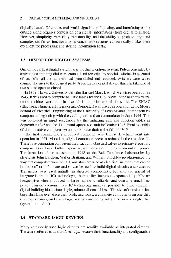
Figure 1.1 shows the general architecture of PLAs and PALs. The most common
housing of PLAs and PALs was a 20-pin dual-in-line package (DIP). The difference
between PALs and PLAs is that in PLA, both the AND and OR planes are
programmable, whereas in PALs, the AND plane is programmable but the OR plane
is fixed. PLAs were expensive to manufacture and offered somewhat poor perfor-
mances, due to propagation delays. Therefore, PALs were introduced for their ease of
manufacturability, lower cost of production, and better performance. PALs usually
contain flip-flops connected to the OR gates to implement sequential circuits. Both
PLAs and PALs use antifuse switches, which remain in a high-impedance state until
programmed into a low-impedance (fused) state. These devices are generally
programmed only once. Generic array logic devices (GALs) are similar to PALs
but can be reprogrammed. PLAs, PALs, and GALs are programmed using a PAL
programmer device (a burner).
4 DIGITAL SYSTEM MODELING AND SIMULATION
1.8 COMPLEX PROGRAMMABLE LOGIC DEVICES
PALs and PLAs are useful for small digital circuits which do not require more than 32
inputs and outputs. To implement circuits that need more inputs and outputs, multiple
PLAs or PALs can be used. However, this will compromise the performance of the
design and also occupy more area on the PCB. In such situations, a complex
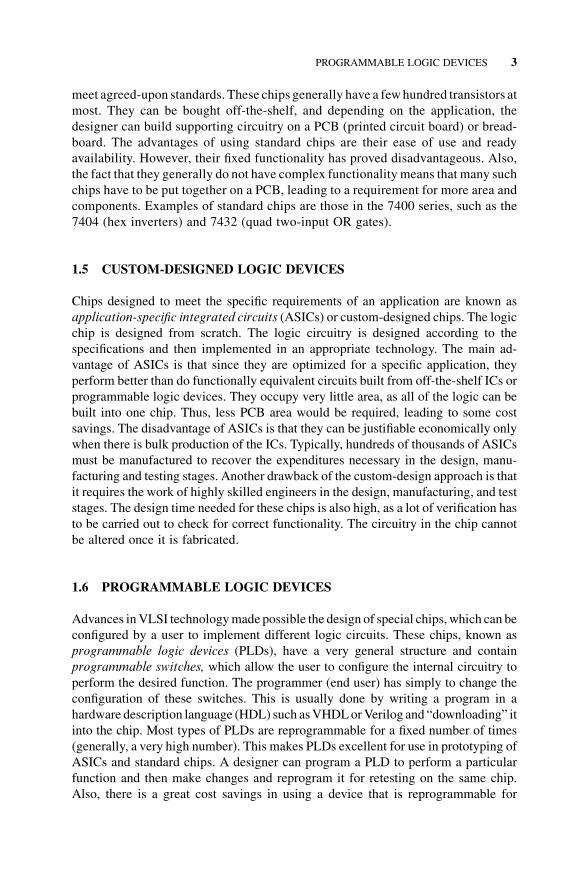
programmable device (CPLD) would be a better choice. ACPLD comprises multiple
circuit blocks on a single chip. Each block is similar to a PLA or PAL. There could be
as few as two such blocks in a CPLD and 100 or more such blocks in larger CPLDs.
These logic blocks are interconnected through a programmable switch matrix or
interconnection array, which allows all blocks of the CPLD to be interconnected.
Figure 1.2 shows the internal structure of aCPLD.As a result of this configuration, the
architecture of the CPLD is less flexible. However, the propagation delay of aCPLD is
...
... .... . .
Inputs
Buffers&
Inverters
ANDPlane
ORPlane
Outputs
Figure 1.1 Schematic Structure of PALs and PLAs
kcol
B O/
I
LogicBlock
LogicBlock
LogicBlock
LogicBlock
Interconnection Array
kcolB
O/I
Figure 1.2 CPLD Internal Structure
COMPLEX PROGRAMMABLE LOGIC DEVICES 5
predictable. This advantage allowed CPLDs to emulate ASIC systems, which operate
at higher frequencies.
1.9 FIELD-PROGRAMMABLE GATE ARRAYS
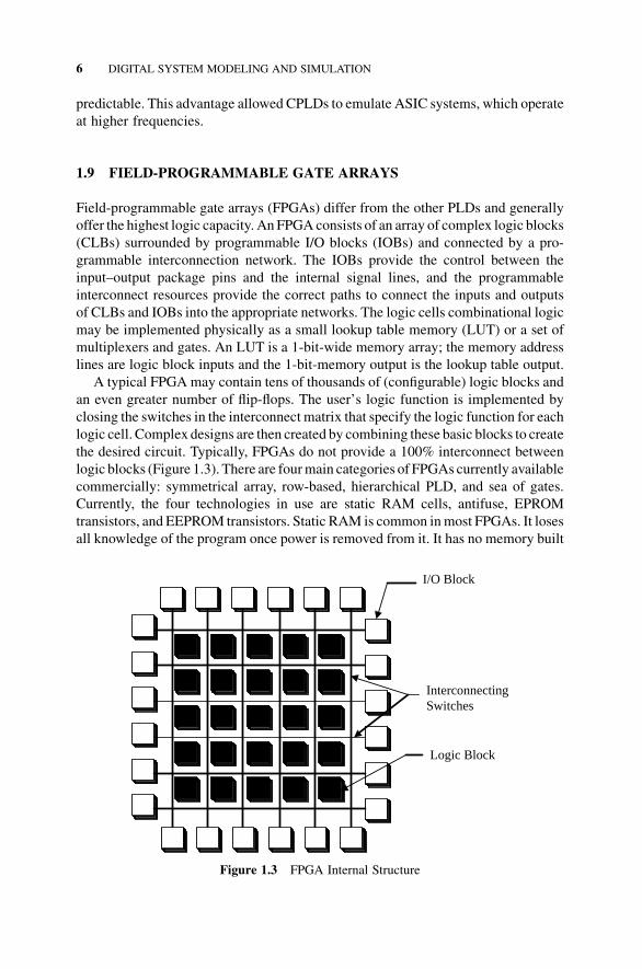
Field-programmable gate arrays (FPGAs) differ from the other PLDs and generally
offer the highest logic capacity. AnFPGA consists of an array of complex logic blocks
(CLBs) surrounded by programmable I/O blocks (IOBs) and connected by a pro-
grammable interconnection network. The IOBs provide the control between the
input–output package pins and the internal signal lines, and the programmable
interconnect resources provide the correct paths to connect the inputs and outputs
of CLBs and IOBs into the appropriate networks. The logic cells combinational logic
may be implemented physically as a small lookup table memory (LUT) or a set of
multiplexers and gates. An LUT is a 1-bit-wide memory array; the memory address
lines are logic block inputs and the 1-bit-memory output is the lookup table output.
A typical FPGA may contain tens of thousands of (configurable) logic blocks and
an even greater number of flip-flops. The user’s logic function is implemented by
closing the switches in the interconnect matrix that specify the logic function for each
logic cell. Complex designs are then created by combining these basic blocks to create
the desired circuit. Typically, FPGAs do not provide a 100% interconnect between
logic blocks (Figure 1.3). There are fourmain categories of FPGAs currently available
commercially: symmetrical array, row-based, hierarchical PLD, and sea of gates.
Currently, the four technologies in use are static RAM cells, antifuse, EPROM
transistors, and EEPROM transistors. Static RAM is common inmost FPGAs. It loses
all knowledge of the program once power is removed from it. It has no memory built
I/O Block
InterconnectingSwitches
Logic Block
Figure 1.3 FPGA Internal Structure
6 DIGITAL SYSTEM MODELING AND SIMULATION

into the chip and upon each power-up must depend on some external source to
upload its memory. EPROM-based programmable chips cannot be reprogrammed
in-circuit and need to be clearedwith ultraviolet (UV) erasing. EEPROMchips can be
erased electrically but generally cannot be reprogrammed in-circuit.
Some FPGA device manufacturing companies are Altera, Cypress, QuickLogic,
Xilinx, Actel, and Lattice Semiconductor. In the early years, Xilinx was a leading
manufacturer and designer of FPGAs. Xilinx produced the first static random access
memory FPGA. The drawback of a SRAMFPGA is the loss of memory after a loss of
power. Actel created a more stable FPGA using antifuse technology. This design
provided a buffer to the loss of memory, kept the cost of each gate low, ran extremely
fast, and provided protection against industrial pirating. SRAMs, were easy to design
however, and the addition of antifuse technology would make the design process
longer. SRAM FPGAs are the majority choice of designers today.
A FPGAvendor usually provides software that “places and routes” the logic on the
device (similar to the way in which a PCB autorouter would place and route
components on a board). There are a wide variety of subarchitectures within the
FPGA family. The key to the performance of these devices lies in the internal logic
contained in their logic blocks and on the performance and efficiency of their switch
matrix. The behavior of an FPGA is accomplished using a hardware descriptive
language (HDL) or an electronic design automation tool to create a design schematic.
When this process is completed, it can be compiled to generate a net list. The net list
can then bemapped to the architecture of the FPGA. The binary file that is generated is
used to reconfigure the FPGA device. The most common hardware descriptive
languages in the design industry are VHDL and Verilog. The design process of
programming an FPGA consists of design entry, simulation, synthesis, place and
route, and download. Design libraries are a common part of the software used in
programming FPGAs. These libraries contain programs of widely used functions and
possess the ability to add new programs provided by the user. Design constraints are
preset by the need for the design and the flexibility of the components reproduced that
are used by the program.
1.10 FUTURE OF DIGITAL SYSTEMS
The latest microprocessors for home computing applications run at about 3GHz.
Most chips available commercially use the bulk-CMOS (complementary metal–
oxide semiconductor) process to manufacture the transistor circuits. Also, most
digital designs are synchronous in nature. Synchronous systems are also referred to as
clocked systems. The latest commercially available chips are manufactured using the
90-nm process. Over the next few years, companies expect to move to 65 nm or lower.
Some experts in the semiconductor industry see an asynchronous future for digital
designs. Asynchronous systems are digital systems that do not use a clock to time
events. Chip size has been shrinking continuously, and designs have become more
complex than ever. Emerging technologies such as hybrid ASIC and LPGA (laser
programmable gate array) make the future exciting. New materials, design
FUTURE OF DIGITAL SYSTEMS 7
methodologies, better fabrication facilities, and newer applications are certainly
making things interesting. The Semiconductor Industry Association (SIA) predicts
that the worldwide per capita production of transistors will soon be 1 billion per
person.
In particular, FPGAs are leading the way to a technological revolution. Many
emerging applications in the communication, computing, and consumer electronics
industries demand that their functionality stays flexible after the system has been
manufactured. Such flexibility is required in order to cope with changing user
requirements, improvements in system features, changing standards, and demands
to support a variety of user applications. With the vast array that FPGAs provide,
hardware design has never been easier to develop or implement. Design revisions can
be implemented effortlessly and painlessly. Currently, they are still under develop-
ment to become faster and easier to program then their CPLD counterparts are now,
but soon the technology will be a reality and the possibility for complete and total
reconfigurable systems will become real. One day, a computer could program itself to
run faster and more efficiently with no help from the user.
PROBLEMS
1.1 What is a digital system?
1.2 Describe computer-aided design software tools.
1.3 Explain Moore’s law.
1.4 What does “PCB” stand for?
1.5 Describe the advantages and disadvantages of standard chips.
1.6 Describe the advantages and disadvantages of programmable logic devices.
1.7 Describe the advantages and disadvantages of custom logic devices.
1.8 Describe the advantages and disadvantages of reconfigurable logic devices.
1.9 Describe the basic design process for digital systems.
8 DIGITAL SYSTEM MODELING AND SIMULATION
2 Number Systems
2.1 OBJECTIVES
The objectives of the chapter are to describe:
. Number systems
. Number conversion
. Data organization
. Unsigned and signed numbers
. Binary arithmetic
. Hexadecimal arithmetic
. Number codes
2.2 BASES AND NUMBER SYSTEMS
The objective of this section is to introduce the various types of number representa-
tions used in digital system designs. The general method for numerical representation
is called positional number representation. Consider the familiar decimal system.
A number in decimal representation is made of digits that range from 0 to 9. Consider
the following decimal number:
ð4261Þ10 ¼ 4� 103þ 2� 102þ 6� 101þ 1� 100
This number is normally written as 4261, as the powers of 10 are implied by the
position of that particular digit. Therefore, a decimal number N with n digits can be
expressed as follows:
ðNÞ10 ¼ dn� 1 � 10n� 1þ dn� 2 � 10n� 2þ � � � þ d1 � 101þ d0 � 100
Decimal representations are said to be base-10 or radix-10 numbers because each
digit has 10 possible values, weighted as a power of 10, depending on the position of
Introduction to Digital Systems: Modeling, Synthesis, and Simulation Using VHDL, First Edition.Mohammed Ferdjallah.� 2011 John Wiley & Sons, Inc. Published 2011 by John Wiley & Sons, Inc.
9
the digit in the number. In a similar way, in binary representation, each binary digit has
two possible values, 1 and 0, and the digits areweighted as a power of 2, depending on
their position in the number. The binary system of representation is also known as a
base-2 system. Consider the following binary number:
ð1001Þ2 ¼ 1� 23þ 0� 22þ 0� 21þ 1� 20 ¼ ð9Þ10Similarly, a binary number N with n digits can be expressed as follows:
ðNÞ2 ¼ dn� 1 � 2n� 1þ dn� 2 � 2n� 2þ � � � þ d1 � 21þ d0 � 20
In general, any numberN can be represented in a base b by the following power series:
ðNÞr ¼ dn� 1 � rn� 1þ dn� 2 � rn� 2þ � � � þ d0 � r0þ d� 1 � r� 1þ � � �þ d�m � r�m
The coefficients (di) are called digits, and r represents the radix or base. In the binary
system the digits are referred to as bits. There are four types of numerical representa-
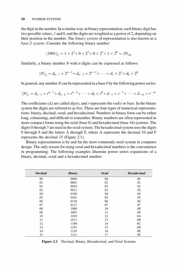
tions: binary, decimal, octal, and hexadecimal. Numbers in binary form can be rather
long, exhausting, and difficult to remember. Binary numbers are often represented in
more compact forms using the octal (base 8) and hexadecimal (base 16) systems. The
digits 0 through 7 are used in the octal system. The hexadecimal system uses the digits
0 through 9 and the letters A through F, where A represents the decimal 10 and F
represents the decimal 15 (Figure 2.1).
Binary representation is by and far the most commonly used system in computer
design. The only reason for using octal and hexadecimal numbers is the convenience
in programming. The following examples illustrate power series expansions of a
binary, decimal, octal and a hexadecimal number.
Decimal Binary Octal Hexadecimal
00 00 0000 00
01 01 0001 01
02 02 0010 02
03 03 0011 03
04 04 0100 04
05 05 0101 05
06 06 0110 06
07 07 0111 07
08 10 1000 08
09 11 1001 09
0A 12 1010 10
0B 13 1011 11
0C 14 1100 12
0D 15 1101 13
0E 16 1110 14
0F 17 1111 15
Figure 2.1 Decimal, Binary, Hexadecimal, and Octal Systems
10 NUMBER SYSTEMS
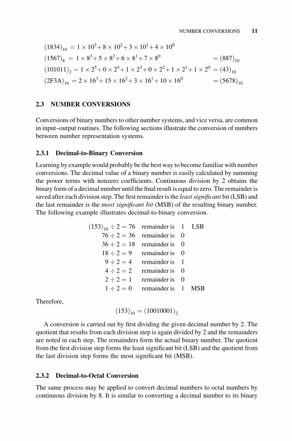
ð1834Þ10 ¼ 1� 103þ8� 102þ3� 101þ4� 100
ð1567Þ8 ¼ 1� 83þ5� 82þ6� 81þ7� 80 ¼ ð887Þ10ð101011Þ2 ¼ 1� 25þ0� 24þ1� 23þ0� 22þ1� 21þ1� 20 ¼ ð43Þ10ð2F3AÞ16 ¼ 2� 163þ15� 162þ3� 161þ10� 160 ¼ ð5678Þ10
2.3 NUMBER CONVERSIONS
Conversions of binary numbers to other number systems, and vice versa, are common
in input–output routines. The following sections illustrate the conversion of numbers
between number representation systems.
2.3.1 Decimal-to-Binary Conversion
Learning by examplewould probably be the best way to become familiar with number
conversions. The decimal value of a binary number is easily calculated by summing
the power terms with nonzero coefficients. Continuous division by 2 obtains the
binary form of a decimal number until the final result is equal to zero. The remainder is
saved after each division step. The first remainder is the least significant bit (LSB) and
the last remainder is the most significant bit (MSB) of the resulting binary number.
The following example illustrates decimal-to-binary conversion.
ð153Þ10 � 2 ¼ 76 remainder is 1 LSB
76� 2 ¼ 36 remainder is 0
36� 2 ¼ 18 remainder is 0
18� 2 ¼ 9 remainder is 0
9� 2 ¼ 4 remainder is 1
4� 2 ¼ 2 remainder is 0
2� 2 ¼ 1 remainder is 0
1� 2 ¼ 0 remainder is 1 MSB
Therefore,
ð153Þ10 ¼ ð10010001Þ2A conversion is carried out by first dividing the given decimal number by 2. The
quotient that results from each division step is again divided by 2 and the remainders
are noted in each step. The remainders form the actual binary number. The quotient
from the first division step forms the least significant bit (LSB) and the quotient from
the last division step forms the most significant bit (MSB).
2.3.2 Decimal-to-Octal Conversion
The same process may be applied to convert decimal numbers to octal numbers by
continuous division by 8. It is similar to converting a decimal number to its binary
NUMBER CONVERSIONS 11