introduction on the face of it, solid-state plasma · introduction o n the face of it,...
TRANSCRIPT
Introduction
ON THE FACE OF IT, "SOLID-STATE PLASMA" is a contradiction in terms. How can one have
a plasma (a word derived from the Greek, meaning "plastic" or "fluid" and used to describe a collection of mobile charged particles) and simultaneously a solid, manifestly a crystalline collection of atoms rigidly fixed in a uniform lattice? The answer is to be found in the collective behavior of electrons in the material.
Crystals (except for insulators) contain a number of electrons free to wander about between lattice sites. These electrons are largely responsible for the current-carrying properties of the solid; they also contribute to the infrared and optical characteristics of the material in a way that depends, among other things, upon their concentration nco The progression from a nearly insulating, optically transparent crystal such as diamond, through the silversheened semiconductors like silicon or germanium, to the highly conducting metals is best typified by a monotonic increasing electron concentration. At any concentration, there exists a characteristic frequency W p , the plasma frequency, equal to (47rnce2/ mEL) !, for which the crystal becomes transparent to electromagnetic radiation of angular frequency w> Wp. Here e and m are the carrier charge and effective mass respectively, and El is the lattice or background dielectric constant. In impure diamond at room temperature, Wp may be in the radiofrequency range; in semiconductors, it is in the infrared, while in the alkali metals (Na, K, etc.), it lies in the near-ultraviolet. The existence of this ubiquitous cutoff frequency at which reflection of electromagnetic waves occurs is due to a cooperative, fluid-like motion of the conduction electrons and holes in response to the waves; it is this collective response, virtually identical to that existing in ionized gas plasma, that leads to the name "solidstate plasma" for mobile carriers.
Why is one interested in solid-state plasmas? Aside from the usual scientific reasons falling under the heading of Natural Philosophy, there are compelling practical motivations well known to technologists: Devices. By properly utilizing the plasma characteristics of certain semiconductors, one might hope to construct miniaturized microwave and infrared sources, magnetically-tuned lasers and band-pass filters, sensitive infrared and optical detectors and, to a limited extent, small-sized solidstate analogs to the very large (and hence expensive)
2
CYCLOTRON RESONANCE IN SOLID-STATE PLASMA
T.O. Poehler and J.R. Ape!
prototype controlled thermonuclear reactors under study by gas plasma physicists the world over.
In most of these applications, an externallyimposed magnetic field B plays an important roleit establishes in the solid a second characteristic frequency, the electron cyclotron frequency We = eB/ mc, where B is the magnetic field in gauss and c is the velocity of light. Recall that this frequency is the angular rate at which an electron gyrates in a magnetic field; it also causes a striking anisotropy in the propagation features of any electromagnetic wave traversing the sample. It may serve to control and channel the plasma in somewhat the same fashion as occurs in a magnetically confined gas plasma. It is this magnetic field that lends much of the interest to the subject, allowing not only variety and flexibility in the devices that utilize it, but introducing, as it does, significant changes in the quantum states of a conduction electron and in its interaction with the other fundamental excitations of the solid-photons, phonons, plasmons, and the like. It is to the investigation of such interactions that the solid-state plasma activity at the Applied Physics Laboratory is addressed.
Semiconductor Properties The majority of the experiments described here
have been conducted in those materials called compound semiconductors.l These materials are generally binary compounds between elements of groups II and VI, or groups III and V of the periodic table, such as GaAs and InSb. These semiconductors crystallize in the zinc-blende or wurtzite structures which are similar to the diamond structure of the
1 Physics of III-VI Compounds, Willardson and Beer, Ed., Academic Press, New York, 1966.
APL T echnical Digest
Electrons and holes in a semiconductor form a solid-state plasma having many unusual features. When cooled to low temperatures and placed in a large magnetic field, such a plasma interacts with far-infrared laser radiation and with ionized impurities in a distinctly quantum-mechanical fashion.
elemental semiconductors, germanium and silicon. The energy band structure of these compounds is analogous in many respects to that of the elemental semiconductors because of the close relationship of the crystal structures.
The energy band structure of a semiconductor is an important factor in determining the movement of charge carriers causing a transport of charge or energy through the material. Under the influence of an electric field E, the electrons and holes move in opposite directions along the field leading to a current density J, where J = uE = e(nc/J-n + p/J-p)E. Here the conductivity, u, is related to nc and p , the concentration of electrons and holes respectively, and /J-n and /J-p are the respective mobilities of these charge carriers. The quantity which characterizes charge transport is the mobility, /J-, which is the ratio of the average velocity of the carriers to the electric field strength ; further, /J- = eT / m, where m is the effective mass of the carriers and T the mean time between collisions. At room temperature the mobility in relatively pure semiconductors is limited owing to scattering of electrons and holes by acoustic or optical phonons, the quantized vibrational excitations of the crystal lattice. In compound semiconductors, scattering of carriers by optical phonons plays the dominant role while at low temperatures the limit on mobility is determined by scattering by ionized impurities. The mobility at a given temperature and impurity concentration is then given by
1/ /J- = 1/ /J-impurity + 1/ /J-Iatt ice.
The charge carriers contributing to the conductivity arise either through the creation of an electron-hole pair by excitation of an electron from the uppermost valence band to the conduction
May - June 1970
band, or by excitation of free carriers from impurity levels in the energy gap between bands. At room temperatures both carrier generation mechanisms contribute to the conductivity, but at low temperatures where the thermal excitation of carriers across the band gap becomes negligible, the free charge carriers are predominantly those excited from impurity levels. Since a given semiconductor material usually has either a large number of donor impurities contributing excess electrons to the conduction band, or a large number of acceptor impurities leading to holes in the valence band, low temperature conduction is generally controlled predominantly by one type of carrier.
The relation between current density and electric field, J = nce/J-nE , (for conduction by electrons) is not in general a linear one. At high electric fields and low lattice temperatures, electrons may gain sufficient energy from the field to ionize previously neutral impurity atoms on collision in the so-called impact ionization process. The electrons which have derived extra energy from the electric field can also be considered to be at a higher temperature than the background lattice-these are called hot electrons. Since the mobility is a function of temperature, these electrons will have a mobility which depends on the applied field strength. Thus, there will be increasing deviations from a linear equation at high electric fields through variations in both carrier concentration and the mobility. .
As a class the III-V compound semiconductors are typified by a wide range of energy gaps, low effective electronic masses, high electron mobilities, and high conductivity. These characteristics are shown quantitatively in Table 1. The number of charge carriers ni in an intrinsic semiconductor depends on the energy gap (, y and the temperature T in an exponential fashion , that is, ni ex: exp( - (,y /
2kBT) where kB is Boltzmann's constant. Most of the compounds have sufficiently large energy gaps that the number of carriers in a pure material should be quite small. However, as the temperature is reduced the carrier concentration in each of these materials reaches a constant value essentially independent of temperature. The cause of this excessive minimum value is the existence of imperfections in the structure of the crystal. The imperfections can be either in the form of foreign impurity atoms introduced into the crystal or deviations from stoichiometry, that is, where the elements in the compound are present in an improper proportion.
3
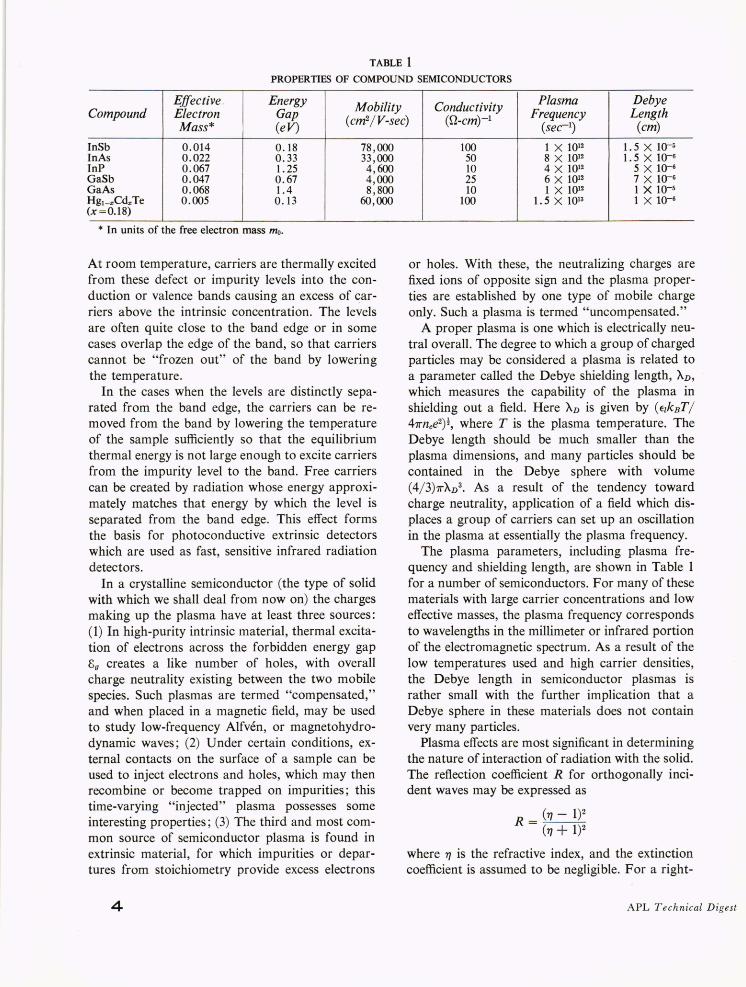
TABLE 1 PROPERTIES OF COMPOUND SEMICONDUCTORS
~ffective - Energy Mobility Conductivity Plasma Debye Compound Electron Gap Frequency Length
Mass * (eV) (cm2 I V-sec) (fl-cm)-I (sec-I) (cm)
InSb 0.014 0.18 78,000 InAs 0.022 0.33 33,000 InP 0.067 1. 25 4,600 GaSb 0.047 0.67 4,000 GaAs 0.068 1.4 8,800 HSI_",Cd",Te 0.005 0.13 60,000 (x=0.18)
* In units of the free electron mass mo.
At room temperature, carriers are thermally excited from these defect or impurity levels into the conduction or valence bands causing an excess of ~arriers above the intrinsic concentration. The levels are often quite close to the band edge or in some cases overlap the edge of the band, so that carriers cannot be "frozen out" of the band by lowering the temperature.
In the cases when the levels are distinctly separated from the band edge, the carriers can be removed from the band by lowering the temperature of the sample sufficiently so that the equilibrium thermal energy is not large enough to excite carriers from the impurity level to the band. Free carriers can be created by radiation whose energy approximately matches that energy by which the level is separated from the band edge. This effect forms the basis for photoconductive extrinsic detectors which are used as fast, sensitive infrared radiation detectors.
In a crystalline semiconductor (the type of solid with which we shall deal from now on) the charges making up the plasma have at least three sources: (1) In high-purity intrinsic material, thermal excitation of electrons across the forbidden energy gap 80 creates a like number of holes, with overall charge neutrality existing between the two mobile species. Such plasmas are termed "compensated," and when placed in a magnetic field, may be used to study low-frequency Alfven, or magnetohydrodynamic waves; (2) Under certain conditions, external contacts on the surface of a sample can be used to inject electrons and holes, which may then recombine or become trapped on impurities; this time-varying "injected" plasma possesses some interesting properties; (3) The third and most common source of semiconductor plasma is found in extrinsic material, for which impurities or departures from stoichiometry provide excess electrons
4
100 1 X 10¹² 1. 5 X 10⁻⁵
50 8 X 10¹² 1. 5 X 10⁻⁶
10 4 X 10¹² 5 X 10⁻⁶
25 6 X 10¹² 7 X 10- 6
10 1 X 10¹² 1 X 10⁻⁵
100 1. 5 X 10¹³ 1 X 10⁻⁶
or holes. With these, the neutralizing charges are fixed ions of opposite sign and the plasma properties are established by one type of mobile charge only. Such a plasma is termed "uncompensated."
A proper plasma is one which is electrically neutral overall. The degree to which a group of charged particles may be considered a plasma is related to a parameter called the Debye shielding length, AD, which measures the capability of the plasma in shielding out a field. Here AD is given by (€lkBT I 47rnce2) !, where T is the plasma temperature. The Debye length should be much smaller than the plasma dimensions, and many particles should be contained in the Debye sphere with volume (4/3) 7rAD3. As a result of the tendency toward charge neutrality, application of a field which displaces a group of carriers can set up an oscillation in the plasma at essentially the plasma frequency.
The plasma parameters, including plasma frequency and shielding length, are shown in Table 1 for a number of semiconductors. For many of these materials with large carrier concentrations and low effective masses, the plasma frequency corresponds to wavelengths in the millimeter or infrared portion of the electromagnetic spectrum. As a result of the low temperatures used and high carrier densities, the Debye length in semiconductor plasmas is rather small with the further implication that a Debye sphere in these materials does not contain very many particles.
Plasma effects are most significant in determining the nature of interaction of radiation with the solid. The reflection coefficient R for orthogonally incident waves may be expressed as
where 'YJ is the refractive index, and the extinction coefficient is assumed to be negligible. For a right-
APL Technical Digest

handed polarized beam propagating through a substance with wave vector k parallel to an applied magnetic field B, the index is
~2 = ,'[1 - w(ww~ w,J
where We is the cyclotron frequency. Total reflection occurs when fJ = 0 so that for radiation to propagate through the medium when B = 0, the radiation frequency must exceed the plasma frequency. For a nonzero magnetic field value this condition is relaxed only slightly in most real cases. Thus, experiments based on the interaction of radiation with the semiconductors shown in Table I must be done at millimeter wavelengths.
Photon Interactions with Semiconductors
Consider an uncompensated solid-state plasma consisting of electrons with an isotropic effective mass m and Lande g-factor g, held at a low temperature T and placed in a large axial magnetic field B = Bi. The electrons scatter from ionized impurities and from phonons, surrendering momentum and energy in the process. This situation obtains in indium antimonide at fields above a few kilogauss and at cryogenic temperatures ; in such material, ionized impurity scattering dominates at liquid helium temperatures (,.....,4°K), while at the boiling point of nitrogen, 77°K, scattering by acoustic phonons governs the resistivity.2 The very small effective electron mass of 0.0135 mo (where mo is the free electron mass) and its large, negative g-factor of - 50 make InSb a favorite material for solid-state plasma experiments. In addition, the energy-momentum relation for conduction electrons at zero magnetic field, S(k), is very nearly the same as for a free electron except for the substitution of m for mo, so that
fPk2 1i2
S(k) ,....., 2m = 2m (k; + k~ + k~) . (1)
Here 11 is Planck's constant h/ 27r, S the total electron energy, and k the wave vector. (Actually, the energy band structure is considerably more complicated than the simple parabolic relation given by Eq. (1) ; such non parabolic effects are important in InSb, but are ignored here for simplicity.)
2 J . R. Apel and T . O. Poehler, Study in L ine and Shape : Cyclotron Resonance in InSb Using an Infrared L aser, APL/ JHU TG 1111, Sept. 1970.
May - June 1970
The imposition of a large magnetic field changes the electronic wave functions dramatically by quantizing the " perpendicular" energy 112(k; + k;)/ 2m at a value (n + ±)11we where n = 0,1,2, ... ; and splitting the degenerate magnetic sub-bands into two states differing in energy by ± 11wegm/ 2mo. However, the component of momentum 11kz (and hence energy) along the direction of the magnetic field is unaltered. The free-electron effective-mass approximation now yields for the B-dependent energy
112k
2 ( gm) S(n,kz,s) ,....., 2m
z + liwc n + ± ± 2mo (2),
where S = ± 1 denote the spin-split levels. In Eq. (2) the term in (n + ±) liwc will be recognized as the energy of a quantum mechanical harmonic oscillator of natural frequency equal to the cyclotron frequency, while that in kz is for a free particle
moving in one dimension. Figure I illustrates the first few levels of S(n,kz,s) , the so-called spin-split Landau levels; because of the negative g-factor, the s = - level is above the one at s = +. At temperatures sufficiently low such that kBT / liwc « 1, only the ground state (n = 0, s = +) is populated; this situation is termed the extreme quantum limit and is reached in InSb at 4°K with a field of only a few kilogauss.
If a solid possessing these characteristics is now illuminated with electromagnetic radiation whose frequency is above the plasma frequency, so that
n =O n = 2 n = 1
WAVE NUMBER ALONG MAG ETIe FIELD, k,
Fig. l-lnSb energy levels in a magnetic field, showing the first three pairs of spin-split Landau levels. The cyclotron resonance transition is denoted by hw, and the most important impurity transition byacj.
5
the radiation penetrates the bulk of the material, the carriers will absorb a portion of the incident power. Assume the wave to be nearly monochromatic (as is radiation from a laser or a source with very narrow-band filtering) and view it as a flux of monoenergetic photons ; one may then adjust the magnetic field so that the difference in energy between any two Landau levels is equal to the photon energy. Then the photons are resonantly absorbed by the free electrons, exciting the electrons to a higher energy state as shown in Fig. 1. This resonant absorption of incident radiation will be observed as a well-defined absorption peak only if T, the mean time between collisions, is sufficiently long so that WeT» 1. The shape of the cyclotron resonance line, i.e. , the plot of absorbed photon flux vs. magnetic field, will depend strongly upon the effective mass of the electron, the kind and frequency of scattering in which it participates, and the temperature at which the measurement is made.
Associated with each of the conduction band Landau levels in the magnetic field is an impurity energy level, as is illustrated in Fig. 1. The change in energy accompanying a transition from the lowest impurity level to the next higher level is designated as Ll8i. At low temperatures when the ground state level is occupied, photons of the proper energy (hv = Ll8i) will excite electrons between these levels. This impurity transition will lead to a resonant absorption of photons which must be separated from the cyclotron resonance of conduction band electrons in the interpretation of the experimental data.
The shape of the electron cyclotron resonance line is determined by the electron scattering which is characterized by the scattering time, T. At room temperature, electrons are scattered by the appreciable number of phonons, the thermally excited lattice vibrations. At temperatures where electronphonon collisions are the dominant scattering mechanism, scattering times are short and any resonance lines observed will be rather broad. At low temperatures the phonon population is small, and the electrons interact instead with ionized impurities by Coulomb scattering. The interaction between the electron and the impurity atom is not a classical Coulomb collision between charged particles because the impurity ion is "screened" from the electron by the other electrons which surround the ion. That is, the electron concentration near the impurity ion is perturbed in such a way that the electric field of the charge is essentially
6
canceled by the rearrangement in the electron distribution. There exists the Debye screening length, AD, within which the screening is ineffective and outside which the effect is more complete. The screening is effective for frequencies less than the plasma frequency so that only short range scattering can occur with a scattering time TO:: 1/ B. For frequencies above the plasma frequency, the shielding effect is greatly reduced due to the inability of the electrons to follow frequencies much above W p ; the ion then appears unshielded, and the scattering time T is an increasing function of B. Thus, the quantum mechanics of Coulomb collisions leads to a kind of decreasing AC magneto resistance at infrared frequencies. This is opposite to the DC
magnetoresistance effect where the resistance of the specimen increases in higher magnetic fields.
Infrared Lasers. Detection. and Optics
The source of radiation for the work described here is the far-infrared gas laser. The gas molecules in the lasers are in the ground electronic state, but are elevated to highly excited vibrational and rotational states by an energetic electrical discharge. As the molecules fall back to the unexcited state through a series of one or more transitions, a radiative transition may occur leading to the emission of an infrared photon.
In the work described here on far-infrared gas lasers the molecules of interest are poly atomic consisting of more than two atoms. These are classified according to the relation between the moments of inertia about the principal axes of symmetry of the molecule when considered as a rigid rotating body. If all three moments are different, the molecule is called an asymmetric top ; if at least two of the principal moments are equal, it is a symmetric top. There are two special cases of the symmetric top: the spherical top with all three moments equal and the linear molecule in which the atoms lie along a straight line giving two equal moments and one of approximately zero magnitude. The laser molecules CO2 and HCN are both linear molecules while H2 0 is an asymmetric top. The actual molecular spectra are complicated by the existence of vibrational-rotational coupling, anharmonicity, perturbations between levels, and interacting modes. The normal modes of vibration for these important classes of
APL T echnical D igest

1'1 ~ • • • • •
"l 1 1 ;; v.
~ • • • • • • LINEAR MOLECULES
(CO •• HCN) NON-LINEAR
MOLECULES (H.o)
Fig 2-Normal vibrations of triatomic laser molecules.
far-infrared laser molecules are shown in Fig. 2. The vibrational state of each of these polyatomic molecules is described by three vibrational quantum numbers, one for each of the vibrational modes.
An energy level diagram showing some of the pertinent vibrational-rotational levels of the HCN molecule is shown in Fig. 3. The vibrational levels involved in the strongest laser transitions are the 1110 and 04°0 levels at values of J from 8 to 11. The transitions between different vibrational states are allowed by dipole selection rules but would normally have very small transition probabilities. However, a Corio lis perturbation between the 1110 and 04°0 states results in mixing of vibrational states for the nearly degenerate levels at the values of J = 9,10,11. The vibrational-rotational transitions at 337 fLm and 311fLm acquire an intensity comparable to that of the strong rotational transitions. The intense transition at 337JLm causes a subsequent inversion of rotational populations in each of the vibrational states leading to pure rotational emission lines at 310fLm and 335 /Lm. This "cascade" effect is an important cause of laser transitions in many infrared lasers including H20 and HeN. A similar series of vibrational-rotational transitions between the 12°0, 0510, and 1220 levels yields a series of shorter laser lines grouped about 130fLm. An analogous series of transitions exists in the H20 molecule except that the more complicated asymmetric-rotor selection rules permit additional cases of cascade and also competing lines.
May-June 1970
d
J=27- c
d
1=26 c
1=2S~ ~.9~ :
1=24- _ t
-J =27 +
+ 1 =26
d!C ==:;1 = 25 +
1200 COSIO 12"0 VIBRATIONAL STATES -
1 = 12==::;:=::::::; +
2841'
-------1 = 11 3101'
1 = 10 ==:f.:;::::::::: --...... --+ ... 1 = 10
3351'
J=9 _____ ~
3731' 1=8 __________ ~ ____ ~ ____ tJ=8
1110 t 0400 VIBRATIONAL STATES----
Fig. 3-Energy level diagram for HeN laser, showing the important emission lines.
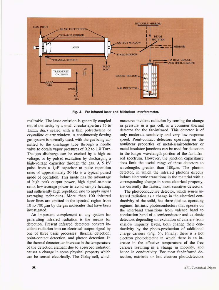
The infrared laser emission lines are generated in a gas discharge laser shown in Fig. 4. 3,4 For molecular lasers, the discharge tubes are several meters in length, since the power generated is proportional to path length of the active medium. Large diameter (7 to 15 cm) tubes are generally used to prevent collisions of gas molecules with the walls from affecting the center of discharge. An optical cavity consisting of a plane fixed mirror and a tunable spherical mirror is mounted inside the vacuum system. This mirror configuration, which is called a semi-confocal cavity, is a low-loss, high-stability one. Since most optical materials do not transmit in the far-infrared portion of the spectrum, mirrors with partially reflecting coatings, as used in visible lasers, are not
3 R. Turner, A. K. Hochberg, and T . O. Poehler, "Multiple Pulse Emission from a HeN Laser," Appl. Phys. Letters 12, Feb 1, 1968, 104-106. 4 R . Turner and T. O. Poehler, "Far-Infrared Laser Interferometry for Electron Density Measurements," 1. Appl. Phys. 39, Nov. 1968, 5726- 5731.
7
GAS INPUT
3MO
BRASS ELECfRODES
12kV
PUMP-! PORT
MOVABLE MIRROR
I i I I " BEAM
OU1PUTWINOOW : I~_ J MJRROR
FIXED MIRROR 1
LIQUID HELIUM
InSbDETECTOR
r---~ TO BIAS CIRCUIT r---~ AND OSCILLOSCOPE _ .. -.. .....
Fig. 4-Far-infrared laser and Michelson interferometer.
realizable. The laser emission is generally coupled out of the cavity by a small circular aperture (5 to 15mm dia.) sealed with a thin polyethylene or crystalline quartz window. A continuously flowing gas system is normally used, with the gas being admitted to the discharge tube through a needle valve to obtain vapor pressures of 0.2 to 1.0 Torr. The gas discharge can be excited by a high DC
voltage, or by pulsed excitation by discharging a high-voltage capacitor through the gas. A 5 kV pulse from a IJLF capacitor at pulse repetition rates of approximately 20 Hz is a typical pulsed mode of operation. This mode has the advantage of high peak output power, high signal-to-noise ratio, low average power to avoid sample heating, and sufficiently high repetition rate to apply signal averaging techniques. More than 100 infrared laser lines are emitted in the spectral region from 10 to 700 JLm by the gas molecules that have been in ves tigated.
An important complement to any system for generating infrared radiation is the means for detection. Present infrared detectors convert incident radiation into an electrical output signal by one of three basic processes : thermal detection, point-contact detection, and photon detection. In the thermal detector, an increase in the temperature of the detection element due to absorbed radiation causes a change in some physical property which can be sensed electrically. The GoJay cell, which
8
measures incident radiation by sensing the change in pressure in a gas cell, is a common thermal detector for the far-infrared. This detector is of only moderate sensitivity and very low response speed. Point-contact detectors operating on the nonlinear properties of metal-semiconductor or metal-insulator junctions can be used for detection in the longer wavelength portion of the far-infrared spectrum. However, the junction capacitance does limit the useful range of these detectors to wavelengths greater than 100,um. The photon detector, in which the infrared photons directly induce electronic transitions in the material with a corresponding change in some electrical property, are currently the fastest, most sensitive detectors.
The photoconductive detector, which senses infrared radiation as a change in the electrical conductivity of the solid, has three distinct operating regimes. Intrinsic photoconductors that operate on the inter band transitions from valence band to conduction band of a semiconductor and extrinsic detectors depending on excitation of carriers from shallow impurity levels, both change their conductivity by the photo-production of additional charge carriers (Fig. 5). Finally, there is a hot electron photodetector in which there is an increase in the effective temperature of the free carriers resulting in a change in mobility, and hence in conductivity. For most far-infrared detection, extrinsic or hot electron photodetectors
APL T echnical Digest

VALENCE BAND
ACCEPTOR -~-LEVEL
Fig. 5-Electronic transitions in photoconductors.
are used ·since most semiconductor band gaps have energies corresponding to visible or near-infrared radiation. Recent advances in growing semiconductor alloys of mixed composition do hold some promise of long wavelength intrinsic detectors.
It is possible to introduce suitable impurities into materials such as silicon, germanium, and gallium arsenide such that energy levels are created in the energy gap. The most useful series consists of the extrinsic germanium detectors shown in Table 2 with their impurity activation energies. Those materials most useful in the farinfrared are Ge: Ga, Ge: Zn, Ge: Hg, and Ge: Au where the levels are shallow; this requires that the detectors be cooled to cryogenic temperatures so that carriers cannot be thermally generated. An even more shallow impurity level exists in GaAs where a donor level has an activation energy of approximatel y 5 me V. This level can be observed in only the best crystalline layers at cryogenic temperatures. These extrinsic detectors which operate by causing electronic transitions are fundamentally quite fast, with ultimate response times of a few nanoseconds, although this is not usually achieved because of circuit limitations.
TABLE 2 IONIZATION ENERGIES OF IMPURITIES IN GERMANIUNl
Impurity element
Gold Mercury Copper Zinc Gallium
Energy(eV)
0.16 0.09 0.04 0.03 0.01
Beyond the long wavelength threshold for extrinsic photoconductivity, the free carrier photoconductive effects can be observed in semicon-
May - June 1970
ductors with high mobilities where the interaction between the free carriers and the crystal lattice is weak. In materials such as InSb and GaAs, the electrons absorb energy from an applied field causing the average electron energy to rise above the thermal equilibrium level. The energy distribution of the electrons will correspond to a thermal distribution at some temperature T e greater than the lattice temperature T. The conductivity will then change to the value at Te rather than the lattice temperature. This electron heating can result in large changes in conductivity and can be caused by applied electric fields or by incident radiation. In InSb, hot electron photoconductivity is observed for wavelengths longer than 100,um, increasing to a maximum at about 1 mm and extending to wavelengths of 1 cm. The relaxation time associated with this type of effect is not equal to that of the direct electronic transitions, leading to fastest response times of approximately 10-7
second. The experiments described here have in general
been concerned with electron cyclotron resonance in semiconducting compounds at far-infrared wavelengths from 48,um to 337,um with the samples at 4.2°K or 77 °K. Initial measurements of the laser emission line wavelengths were made using a Michelson interferometer shown in Fig. 4. Subsequent wavelength measurements and spectral filtering were done using infrared diffraction gratings blazed at 112.5,um and 450,um, respectively.
The optics associated with laser beams in this wavelength regime reflect the quasi-optical, quasimicrowave character of this radiation. The beams can be transmitted with relatively low loss by use of light pipes which are simply oversized waveguides used without mode discrimination. Propagation through these pipes can be described in optical terms by a nearly plane wave passing through the pipe by multiple low angle reflections. These light pipes are most commonly circular in cross section; however, it has been found that square or rectangular light guides can be used to transmit linearly polarized radiation with high efficiency. 5
The far-infrared beams may be focused using thin dielectric lenses most often made from polyethylene. Windows and beam splitters are also
5 T. O. Poehler and R. Turner, "Transmission of Polarized Far Infrared Radiation through Metal Light Pipes," Appl. Optics 9, Apr. 1970, 971-973.
9
~~I ____ UQUID HBUUM
_ CRYOGENIC DETECTORS
Fig. 6-Schematic of cyclotron resonance experiment, as conducted in superconducting magnet.
made using thin high-density polyethylene sheet which together with crystalline quartz are the only materials that readily transmit these wavelengths. Linearly polarized beams can be generated by passing the radiation through a polarizer which may be constructed using a number of thin polyethylene films at the Brewster angle. Alternatively, polarizers can be produced using a fine metallic grid such as aluminum strips on a mylar base with up to 1000 lines per inch. Thin sheets of polyethylene or mylar can also be used for constructing beam splitters where the partially transmitting, partially reflecting film is used to divide the beam into two separate paths. Spectral filtering is primarily accomplished using diffraction gratings, but the transmission characteristics of fused quartz, crystalline quartz, polyethylene, and some instrinsic semiconductors can often be used to advantage.
Some Experimental Results
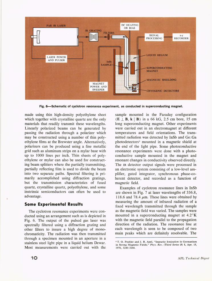
The cyclotron resonance experiments were conducted using an arrangement such as is depicted in Fig. 6. The output of the pulsed gas laser was spectrally filtered using a diffraction grating and other filters to insure a high degree of monochromaticity. The radiation was then transmitted through a specimen mounted in an aperture in a stainless steel light pipe in a liquid helium Dewar. Most measurements were carried out with the
10
sample mounted in the Faraday configuration (E ~ B, k II B) in a 66 kG, 2.5 cm bore, 15 cm long superconducting magnet. Other experiments were carried out in an electromagnet at different temperatures and field orientations. The transmitted radiation was detected by InSb and Ge: Ga photodetectors6 mounted in a magnetic shield at the end of the light pipe. Some photoconductive resonance experiments were done with a photoconductive sample mounted in the magnet and resonant changes in conductivity observed directly. The IR detector output signals were processed in an electronic system consisting of a low-level amplifier, gated integrator, synchronous phase-coherent detector, and recorded as a function of magnetic field.
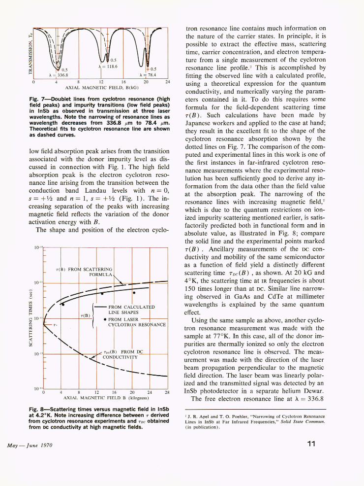
Examples of cyclotron resonance lines in InSb are shown in Fig. 7 at laser wavelengths of 336.8, 118.6 and 78.4 jJ-m. These lines were obtained by measuring the amount of infrared radiation of a fixed wavelength transmitted through the sample as the magnetic field was varied. The samples were mounted in a superconducting magnet at 4.2 OK with the magnetic field parallel to the propagation direction of the radiation. The resonance line at each wavelength is seen to be composed of two main peaks which are definitely resolvable. The
6 T . O. Poehler and J. R. Apel, "Impurity Ionization in Germanium in Strong Magnetic Fields," Phys. Rev. (Third Series B ) 1, Apr. 15, 1970, 3240-3244.
APL T echnical Digest
o 4 8 12 16 24
AXIAL MAGNETIC FIELD, B (kG )
Fig. 7-Doublet lines from cyclotron resonance (high field peaks) and impurity transitions (low field peaks) in InSb as observed in transmission at three laser wavelengths. Note the narrowing of resonance lines as wavelength decreases from 336.8 Ilm to 78.4 Ilm. Theoretical fits to cyclotron resonance line are shown as dashed curves.
low field absorption peak arises from the transition associated with the donor impurity level as discussed in connection with Fig. 1. The high field absorption peak is the electron cyclotron resonance line arising from the transition between the conduction band Landau levels with n = 0, S = +1;2 and n = 1, S = +Yz (Fig. 1). The increasing separation of the peaks with increasing magnetic field reflects the variation of the donor activation energy with B.
tI)
~ :2
The shape and position of the electron cyclo-
10-'O'r------.---,------r---.---.-------.-----,
T(B ) FROM SCATTERING FORMULA
10-1't----+-- +----+----+--'==-= ..... -"""""'~'----l
•
f: T(B) o 1O-12f-1---+---+----'---'- 1
-- FROM CALCULATED LINE SHAPES
• FROM LASER -+------j CYCLOTRON RESONANCE Z
~ Ul
~ <: u tI)
" I 0- 1 3t----+--~-----j,4 TDC (B ) FROM D-....:::C'----1f---_-l CONDUCTIVITY
10-14'-------"---__ -L-_--'-__ -'-__ '--_----"---_-----'
o 4 12 16 20 24 28 AXIAL MAGNETIC FIELD B (kilogauss)
Fig. 8-Scattering times versus magnetic field in InSb at 4.20 K. Note increasing difference between T derived from cyclotron resonance experiments and TD C obtained from DC conductivity at high magnetic fields.
May - June 1970
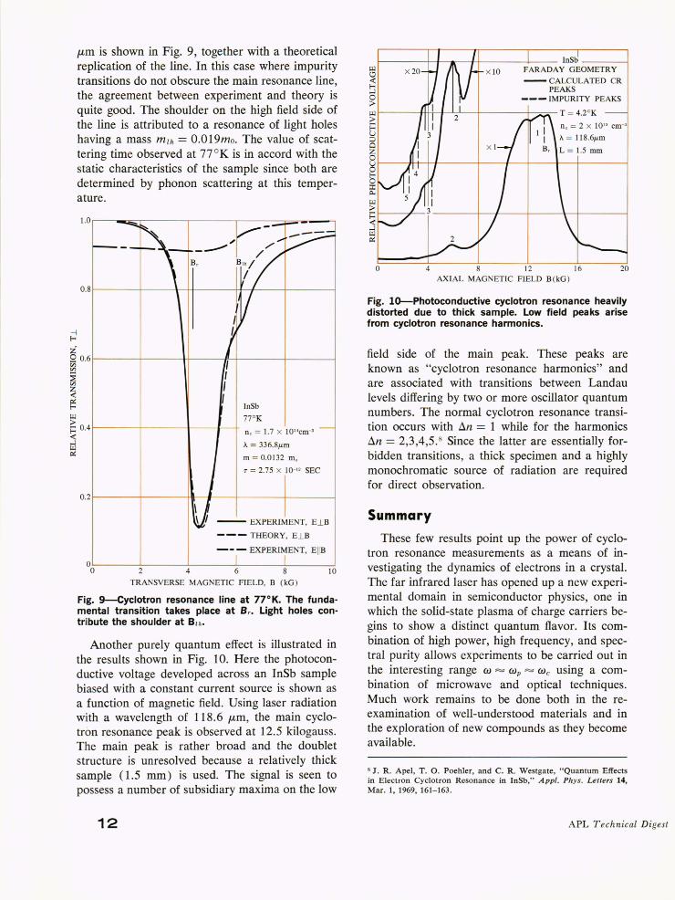
tron resonance line contains much information on the nature of the carrier states. In principle, it is possible to extract the effective mass, scattering time, carrier concentration, and electron temperature from a single measurement of the cyclotron resonance line profile. 2 This is accomplished by fitting the observed line with a calculated profile, using a theoretical expression for the quantum conductivity, and numerically varying the parameters contained in it. To do this requires some formula for the field-dependent scattering time T(B). Such calculations have been made by Japanese workers and applied to the case at hand; they result in the excellent fit to the shape of the cyclotron resonance absorption shown by the dotted lines on Fig. 7. The comparison of the computed and experimental lines in this work is one of the first instances in far-infrared cyclotron resonance measurements where the experimental resolution has been sufficiently good to derive any information from the data other than the field value at the absorption peak. The narrowing of the resonance lines with increasing magnetic field,1 which is due to the quantum restrictions on ionized impurity scattering mentioned earlier, is satisfactorily predicted both in functional form and in absolute value, as illustrated in Fig. 8; compare the solid line and the experimental points marked T(B). Ancillary measurements of the DC conductivity and mobility of the same semiconductor as a function of field yield a distinctly different scattering time T D C (B) , as shown. At 20 kG and 4 OK, the scattering time at IR frequencies is about 150 times longer than at DC. Similar line narrowing observed in GaAs and CdTe at millimeter wavelengths is explained by the same quantum effect.
Using the same sample as above, another cyclotron resonance measurement was made with the sample at 77°K. In this case, all of the donor impurities are thermally ionized so only the electron cyclotron resonance line is observed. The measurement was made with the direction of the laser beam propagation perpendicular to the magnetic field direction. The laser beam was linearly polarized and the transmitted signal was detected by an InSb photodetector in a separate helium Dewar.
The free electron resonance line at A = 336.8
, J. R. Apel and T. O. Poehler, "Narrowing of Cyclotron Resonance Lines in InSb at Far Infrared Frequencies," Solid State Commun. (in publication) .
11
fLm is shown in Fig. 9, together with a theoretical replication of the line. In this case where impurity transitions do not obscure the main resonance line, the agreement between experiment and theory is quite good. The shoulder on the high field side of the line is attributed to a resonance of light holes having a mass m~h = O.OI9mo. The value of scattering time observed at 77 OK is in accord with the static characteristics of the sample since both are determined by phonon scattering at this temperature.
1.or---.;;;;:::-r-------.------.------==--.----.
0.8 t------+---\--+l---+f--+--+---~
-1 E-<
z· 9 0.61----t----t+-----P.-+-----t-------l til til
::@ til Z « ~ InSb
g; 77°K 1= O.4 I-------+----I-----J~-+- ne = 1.7 x 1014cm-3
« ...J ~ ~
A = 336.8/Lm
rn = 0.0132 rno
7' = 2.75 X 10⁻¹² SEC
0.2t--------t----Hl--I-- +----+------l
-- EXPERIMENT, E..lB
--- THEORY, E ..lB
-- - EXPERIMENT, E II B
°0~--~2----4L---~6----L8---~10
TRANSVERSE MAGNETIC FIELD, B (kG )
Fig. 9-cyclotron resonance line at 77°K. The fundamental transition takes place at S r. Light holes contribute the shoulder at B1h•
Another purely quantum effect is illustrated in the results shown in Fig. 10. Here the photoconductive voltage developed across an InSb sample biased with a constant current source is shown as a function of magnetic field. Using laser radiation with a wavelength of 118.6 fLID, the main cyclotron resonance peak is observed at 12.5 kilogauss. The main peak is rather broad and the doublet structure is unresolved because a relatively thick sample (1.5 mm) is used. The signal is seen to possess a number of subsidiary maxima on the low
12
o 4 12 16 20 AXIAL MAG ETIC FIELD B (kG )
Fig. 10-Photoconductive cyclotron resonance heavily distorted due to thick sample. low field peaks arise from cyclotron resonance harmonics.
field side of the main peak. These peaks are known as "cyclotron resonance harmonics" and are associated with transitions between Landau levels differing by two or more oscillator quantum numbers. The normal cyclotron resonance transition occurs with I:1n = 1 while for the harmonics I:1n = 2,3 ,4,5. 8 Since the latter are essentially forbidden transitions, a thick specimen and a highly monochromatic source of radiation are required for direct observation.
Summary
These few results point up the power of cyclotron resonance measurements as a means of investigating the dynamics of electrons in a crystal. The far infrared laser has opened up a new experimental domain in semiconductor physics, one in which the solid-state plasma of charge carriers begins to show a distinct quantum flavor. Its combination of high power, high frequency, and spectral purity allows experiments to be carried out in the interesting range W = W p = W e using a combination of microwave and optical techniques. Much work remains to be done both in the reexamination of well-understood materials and in the exploration of new compounds as they become available.
8 J . R. Ape!, T. O . Poehler, and C. R. Westgate, " Quantum Effects in Electron Cyclotron Resonance in InSb," Appl. Phys. Letters 14, Mar. 1, 1969, 161-163.
APL T echnical D igest