interfacing the c2000™ with an afe030/1: fsk example · 2018-01-11 · this application report...
TRANSCRIPT
1SPRAC94B–June 2017–Revised January 2018Submit Documentation Feedback
Copyright © 2017–2018, Texas Instruments Incorporated
Interfacing the C2000™ With an AFE03x: B-FSK Example
Application ReportSPRAC94B–June 2017–Revised January 2018
Interfacing the C2000™ With an AFE030/1: FSK Example
Vincent Rodriguez, Errol Leon, Kevin Allen
ABSTRACTThis application report provides information on how to interface a C2000 device with an AFE031, andsend and receive data over a wired coupled interface using frequency shift keying. A demonstration oftransmitting FSK information is discussed with tone frequencies in the 130-145 kHz range.
The target processor for the software is the TMDS320F28379D, but the software can be ported to otherdevices. Project collateral and example code discussed in this document can be found in the latestC2000Ware release within the directory:
C:\ti\c2000\C2000Ware_x_xx_xx_xx\device_support\f2837xd\examples\cpu1
The available example projects are:• boostxl_afe031_f28379d_pwmmode• boostxl_afe031_f28379d_dacmode• boostxl_afe031_f28379d_rx
Contents1 FSK Overview ............................................................................................................... 32 Hardware Overview.......................................................................................................... 53 Interfacing With the AFE03x ............................................................................................... 94 Interfacing With a Power Line ........................................................................................... 275 Summary ................................................................................................................... 386 References .................................................................................................................. 38Appendix A Schematics ......................................................................................................... 39
List of Figures
1 Binary FSK in the Time Domain .......................................................................................... 32 Transmitter Example ........................................................................................................ 43 Receiver Example .......................................................................................................... 44 TMDS28379D LaunchPad.................................................................................................. 55 BoosterPack Test Board.................................................................................................... 56 C2000 and AFE031 Block Diagram ....................................................................................... 67 BOOSTXL-AFE031 Power Pins ........................................................................................... 78 BOOSTXL-AFE031 Terminal Block Connections ....................................................................... 79 F28379D Jumper Configuration ........................................................................................... 810 F28379D JP6 Location...................................................................................................... 811 TX-RX Solution System..................................................................................................... 912 PWM Addition .............................................................................................................. 1113 PWM Transmit Path ....................................................................................................... 1214 TX Filter Gain vs. Frequency ............................................................................................ 1215 PWM Mode Mark Frequency, 131.25 kHz .............................................................................. 1316 PWM Mode Space Frequency, 143.75 kHz ........................................................................... 1317 Full Packet Transmission Waveform .................................................................................... 14

www.ti.com
2 SPRAC94B–June 2017–Revised January 2018Submit Documentation Feedback
Copyright © 2017–2018, Texas Instruments Incorporated
Interfacing the C2000™ With an AFE03x: B-FSK Example
18 DAC Transmit Path ........................................................................................................ 1519 DAC Sine Wave Ramp .................................................................................................... 1520 DAC Mode Mark Frequency Spectrum Analyzer ...................................................................... 1721 DAC Mode Space Frequency Spectrum Analyzer .................................................................... 1722 Full Packet Transmission Waveform .................................................................................... 1823 60 Hz Sine Wave........................................................................................................... 1824 100 Hz Sine Wave ......................................................................................................... 1825 60 + 100 Hz Sine Wave ................................................................................................... 1826 FFT of Combined Signals ................................................................................................. 1827 AFE031 Receive Path Interfaced With C2000 ADC .................................................................. 1928 External Filtering for the AFE031 Receive Path ....................................................................... 2029 RX Filter Gain vs. Frequency ............................................................................................ 2130 Received FSK Signal ...................................................................................................... 2231 Packet of Recieved Bits of Data ......................................................................................... 2532 Packetized Data ............................................................................................................ 2533 Simplified Line Coupling Circuit for AC Main .......................................................................... 2834 Coupling Circuit for a DC Line ........................................................................................... 3035 Example of Multiple PLC Modules Coupled to a DC Line ........................................................... 3136 Recommended Transient Protection .................................................................................... 3237 Metal Oxide Varistor (MOV) .............................................................................................. 3238 Typical MOV I/V Characteristic .......................................................................................... 3339 Typical 8/20-µs Pulse for MOV and TVS Performance Specification .............................................. 3440 Bi-Directional TVS Diode ................................................................................................. 3441 Typical Bi-Directional TVS I/V Characteristics ......................................................................... 3542 Typical Signal at the TVS ................................................................................................ 3643 Current Steering Diodes .................................................................................................. 3744 Typical Line Coupling Circuit ............................................................................................. 3745 Schematic PWM Mode - Page 1 ......................................................................................... 4046 Schematic PWM Mode - Page 2 ......................................................................................... 4147 Schematic PWM Mode - Page 3 ......................................................................................... 4248 Schematic PWM Mode - Page 4 ......................................................................................... 4349 Schematic DAC Mode - Page 1 .......................................................................................... 4450 Schematic DAC Mode - Page 2 .......................................................................................... 4551 Schematic DAC Mode - Page 3 .......................................................................................... 4652 Schematic DAC Mode - Page 4 .......................................................................................... 47
List of Tables
1 FSK Specifications ......................................................................................................... 112 External R and C Values to Increase Filter Response in PWM Applications ..................................... 123 Resolution for PWM and HRPWM ....................................................................................... 144 AFE031 RX PGA Gain Settings ......................................................................................... 205 Recommended Rx Filter External Capacitor Values .................................................................. 206 Recommended Component Values for Fourth-Order Passive Bandpass Filter (0-dB Passband
Attenuation) ................................................................................................................ 217 Software Frequency Parameters......................................................................................... 238 C2000 Resources Utilized ................................................................................................ 259 Library Function CPU Cycles ............................................................................................ 2610 Software ISR/Function Usage ........................................................................................... 26
www.ti.com FSK Overview
3SPRAC94B–June 2017–Revised January 2018Submit Documentation Feedback
Copyright © 2017–2018, Texas Instruments Incorporated
Interfacing the C2000™ With an AFE03x: B-FSK Example
TrademarksC2000 is a trademark of Texas Instruments.All other trademarks are the property of their respective owners.
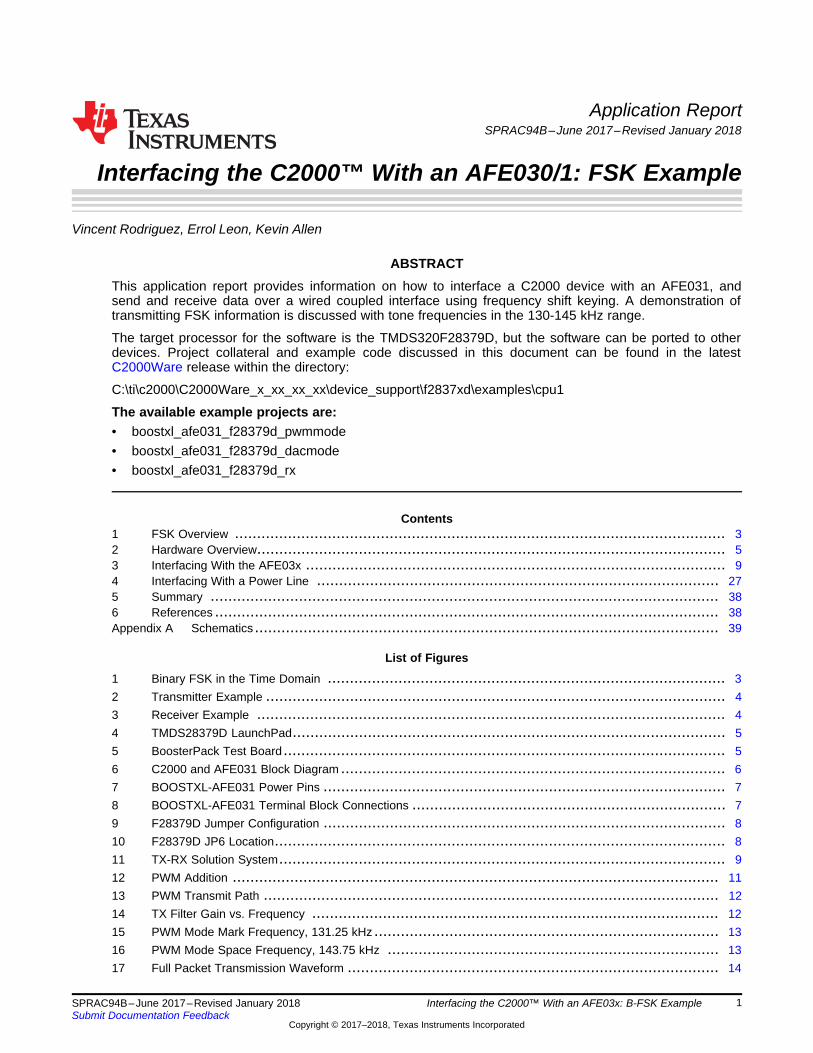
1 FSK OverviewFrequency Shift Keying (FSK) is a modulation scheme that utilizes discrete changes of frequency totransmit and receive digital data. One of the simplest subsections of this modulation scheme, and also themodulation used in this demo, is called Binary Frequency Shift Keying (BFSK).
In this scheme, the system is switching between two discrete frequencies: the Mark Frequency (“1”) andthe Space Frequency (“0”). These frequencies correlate directly to the bit value of the transmitted data.
Figure 1 shows what this looks like in the time domain.
Figure 1. Binary FSK in the Time Domain
Space
Frequency
Mark
Frequency
FSK
Waveform
Binary
Message
0
1
FSK Transmitter
FSK Overview www.ti.com
4 SPRAC94B–June 2017–Revised January 2018Submit Documentation Feedback
Copyright © 2017–2018, Texas Instruments Incorporated
Interfacing the C2000™ With an AFE03x: B-FSK Example
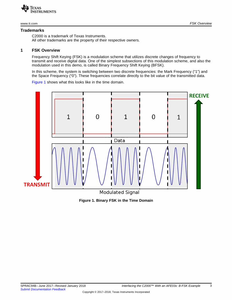
Figure 2 shows an example of a simplified FSK transmitter where the block consists of two oscillators withan internal clock as well as an input binary sequence to control the position of the switch.
Figure 2. Transmitter Example
The two oscillators, producing a higher (space) and a lower (mark) frequency signals, are connected to aswitch along with an internal clock. A clock is applied internally to both oscillators to avoid phasediscontinuities of the output waveform during the transmission of the message. The binary input sequenceis applied to choose the frequencies according to the binary input. In this case, binary "0" corresponds tothe output of the space frequency and binary "1" corresponds to the output of the mark frequency.
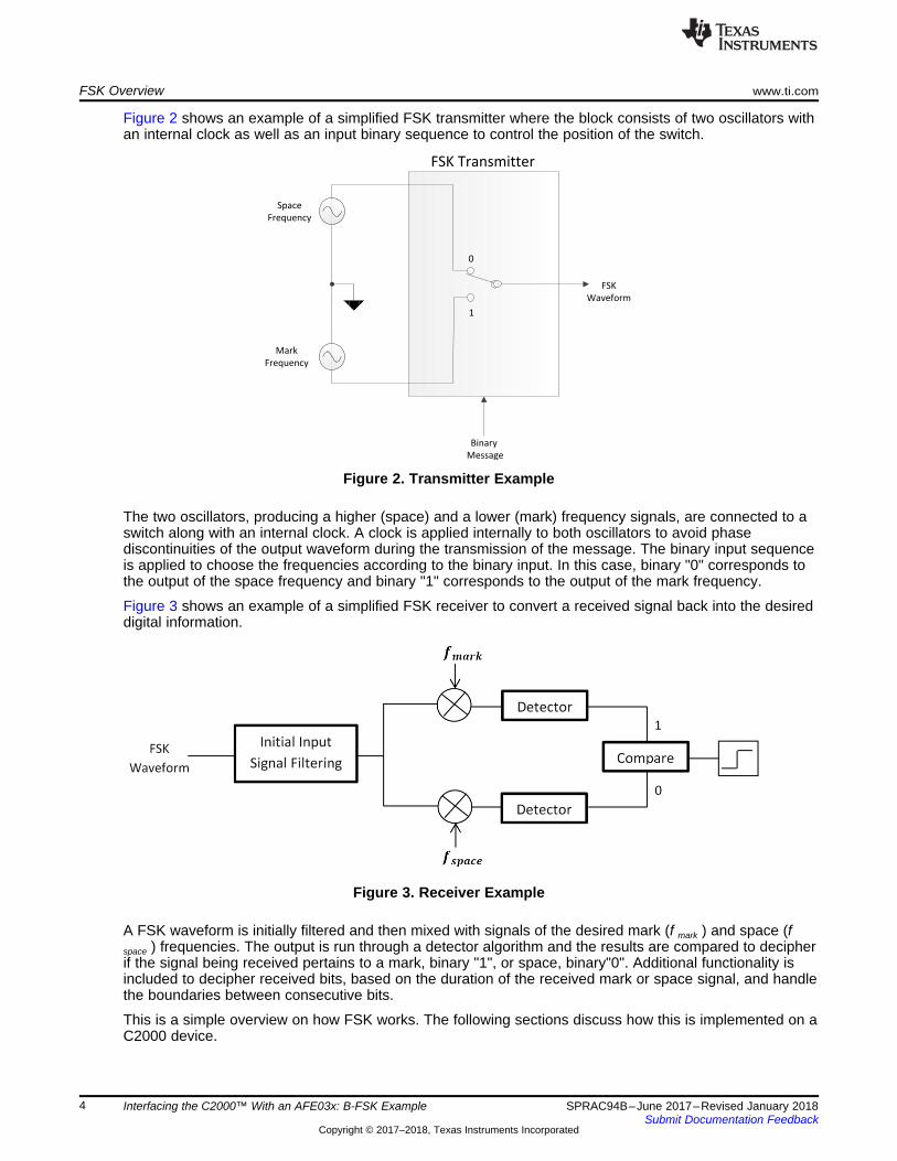
Figure 3 shows an example of a simplified FSK receiver to convert a received signal back into the desireddigital information.
Figure 3. Receiver Example
A FSK waveform is initially filtered and then mixed with signals of the desired mark (f mark ) and space (fspace ) frequencies. The output is run through a detector algorithm and the results are compared to decipherif the signal being received pertains to a mark, binary "1", or space, binary"0". Additional functionality isincluded to decipher received bits, based on the duration of the received mark or space signal, and handlethe boundaries between consecutive bits.
This is a simple overview on how FSK works. The following sections discuss how this is implemented on aC2000 device.
www.ti.com Hardware Overview
5SPRAC94B–June 2017–Revised January 2018Submit Documentation Feedback
Copyright © 2017–2018, Texas Instruments Incorporated
Interfacing the C2000™ With an AFE03x: B-FSK Example
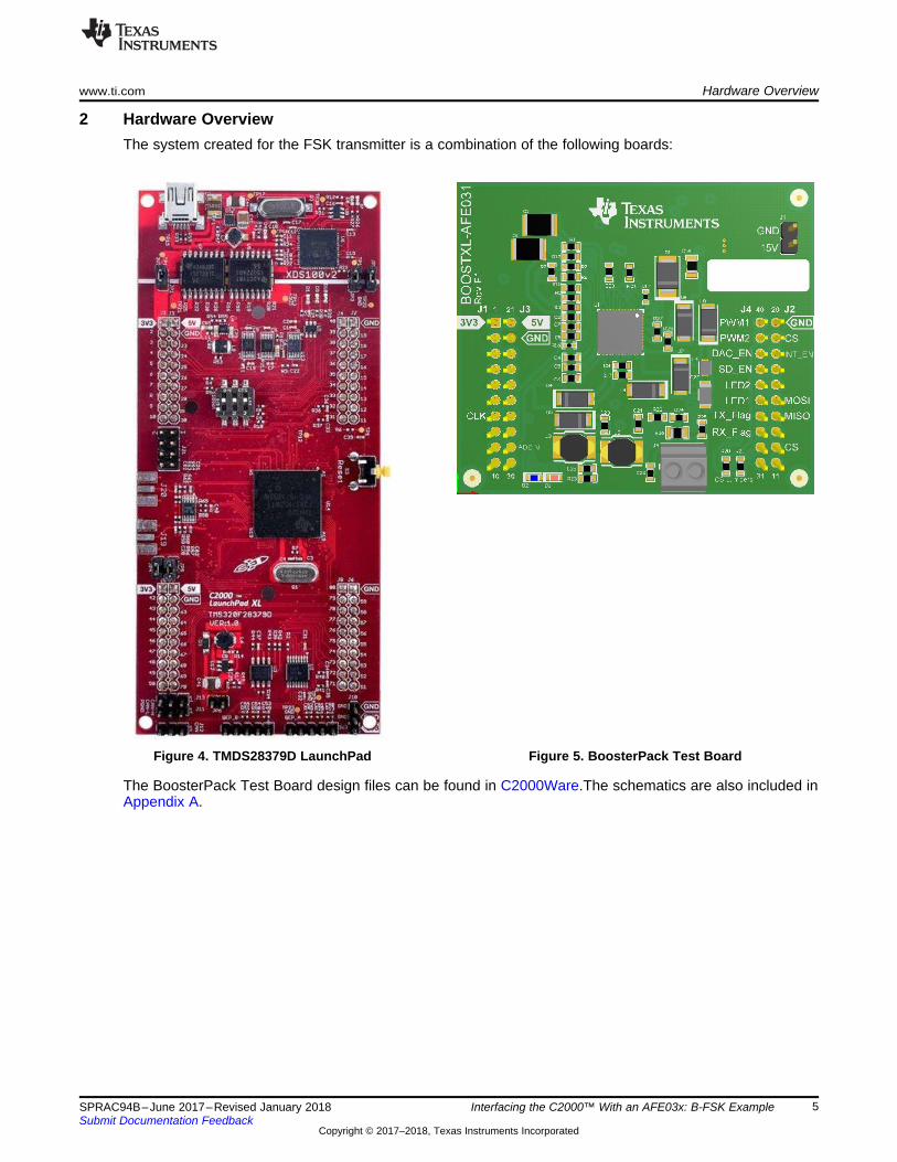
2 Hardware OverviewThe system created for the FSK transmitter is a combination of the following boards:
Figure 4. TMDS28379D LaunchPad Figure 5. BoosterPack Test Board
The BoosterPack Test Board design files can be found in C2000Ware.The schematics are also included inAppendix A.

Hardware Overview www.ti.com
6 SPRAC94B–June 2017–Revised January 2018Submit Documentation Feedback
Copyright © 2017–2018, Texas Instruments Incorporated
Interfacing the C2000™ With an AFE03x: B-FSK Example
2.1 Block DiagramFigure 6 shows a block diagram of the system. In this example, not all of the connections have beenutilized, but all are present on the BoosterPack for future development.
Figure 6. C2000 and AFE031 Block Diagram
The AFE has multiple internal registers that allow configuration of the internal components of the AFEchip, including filter selection, gain selection, and mode selections. These registers can be accessed usingthe SPI peripheral.
The AFE also has various GPIOs that allow the MCU to set the AFE into certain modes, as well asreceive interrupts for critical events on the AFE. The ADC connection allows the MCU to receive orsample an input signal. The PWM signals provide a way to create an output for the AFE. Currently theAFE031 supports two modes of data transmission, PWM mode and DAC mode. An explanation andimplementation of both of these modes can be found in Section 3.

www.ti.com Hardware Overview
7SPRAC94B–June 2017–Revised January 2018Submit Documentation Feedback
Copyright © 2017–2018, Texas Instruments Incorporated
Interfacing the C2000™ With an AFE03x: B-FSK Example
2.2 Hardware SetupThere are a few things that need to be done so that the hardware can be debugged correctly. Power issupplied to the BOOSTXL-AFE031 test board via the 15 V jumper. The BoosterPack has a regulator thatwill supply power to the LaunchPad connected. Figure 7 shows a close up of the 15 V headers.
Figure 7. BOOSTXL-AFE031 Power Pins
The wire connected to the right input of the terminal block shown in Figure 8 will be the line that thetransmitted output or received input FSK signal resides on, depending on whether the system is set up asa transmitter or receiver. The wire connected to the left input of the terminal block is the ground line.These lines can then be connected to some coupling circuitry or directly to another BOOSTXL-AFE031terminal block for controlled testing, TX/RX to TX/RX and GND to GND.
Figure 8. BOOSTXL-AFE031 Terminal Block Connections
Hardware Overview www.ti.com
8 SPRAC94B–June 2017–Revised January 2018Submit Documentation Feedback
Copyright © 2017–2018, Texas Instruments Incorporated
Interfacing the C2000™ With an AFE03x: B-FSK Example
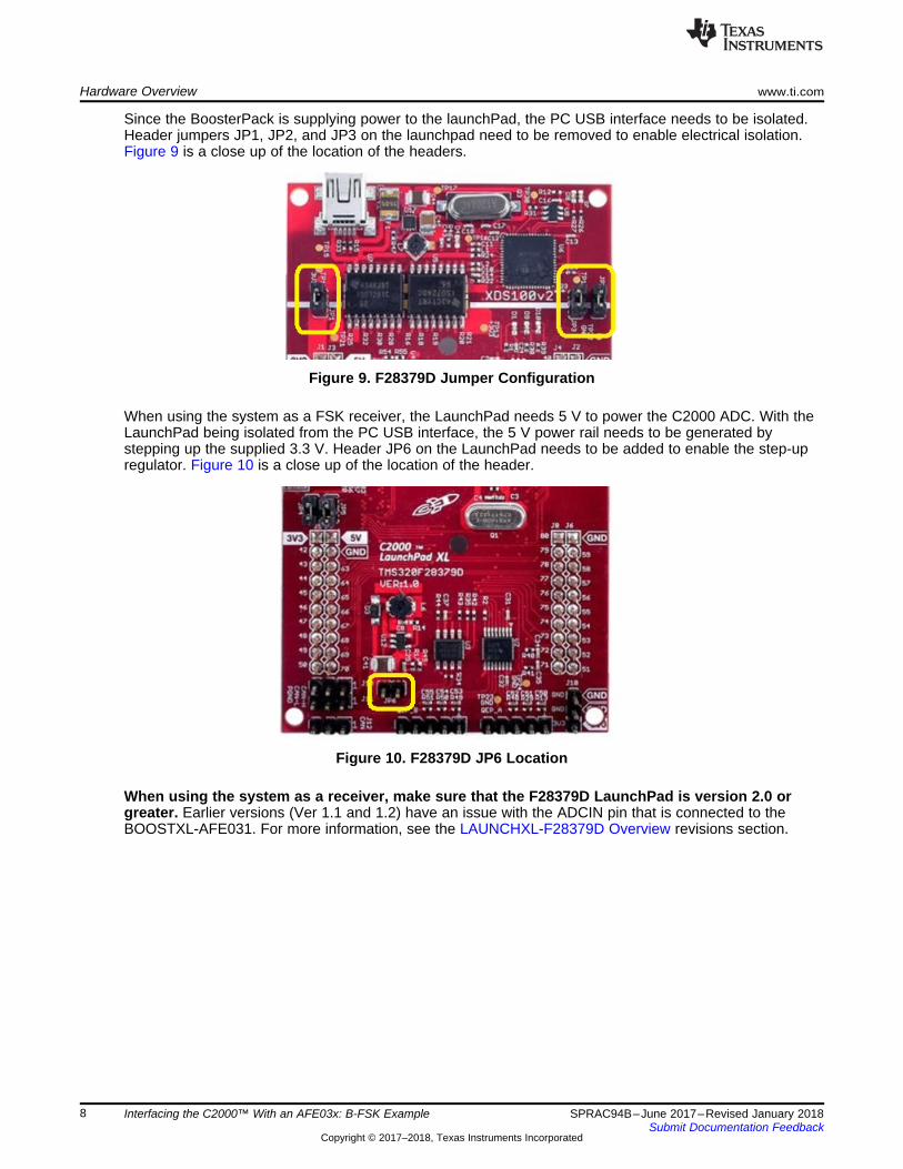
Since the BoosterPack is supplying power to the launchPad, the PC USB interface needs to be isolated.Header jumpers JP1, JP2, and JP3 on the launchpad need to be removed to enable electrical isolation.Figure 9 is a close up of the location of the headers.
Figure 9. F28379D Jumper Configuration
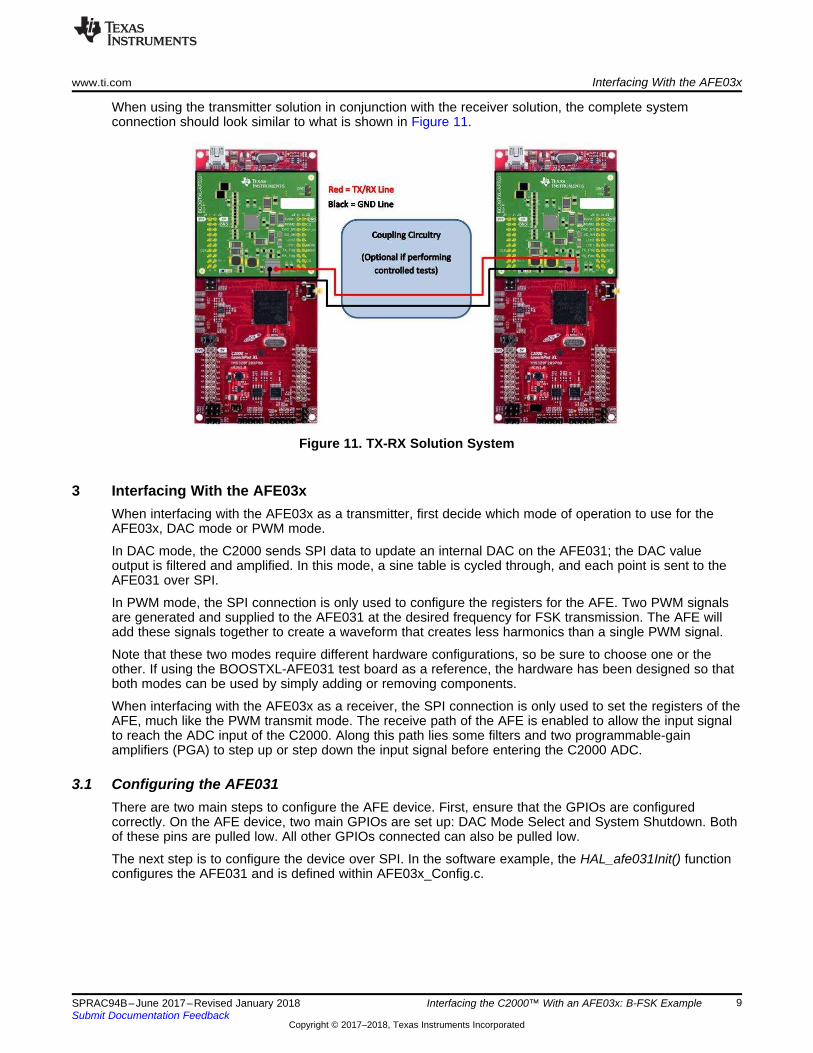
When using the system as a FSK receiver, the LaunchPad needs 5 V to power the C2000 ADC. With theLaunchPad being isolated from the PC USB interface, the 5 V power rail needs to be generated bystepping up the supplied 3.3 V. Header JP6 on the LaunchPad needs to be added to enable the step-upregulator. Figure 10 is a close up of the location of the header.
Figure 10. F28379D JP6 Location
When using the system as a receiver, make sure that the F28379D LaunchPad is version 2.0 orgreater. Earlier versions (Ver 1.1 and 1.2) have an issue with the ADCIN pin that is connected to theBOOSTXL-AFE031. For more information, see the LAUNCHXL-F28379D Overview revisions section.
www.ti.com Interfacing With the AFE03x
9SPRAC94B–June 2017–Revised January 2018Submit Documentation Feedback
Copyright © 2017–2018, Texas Instruments Incorporated
Interfacing the C2000™ With an AFE03x: B-FSK Example
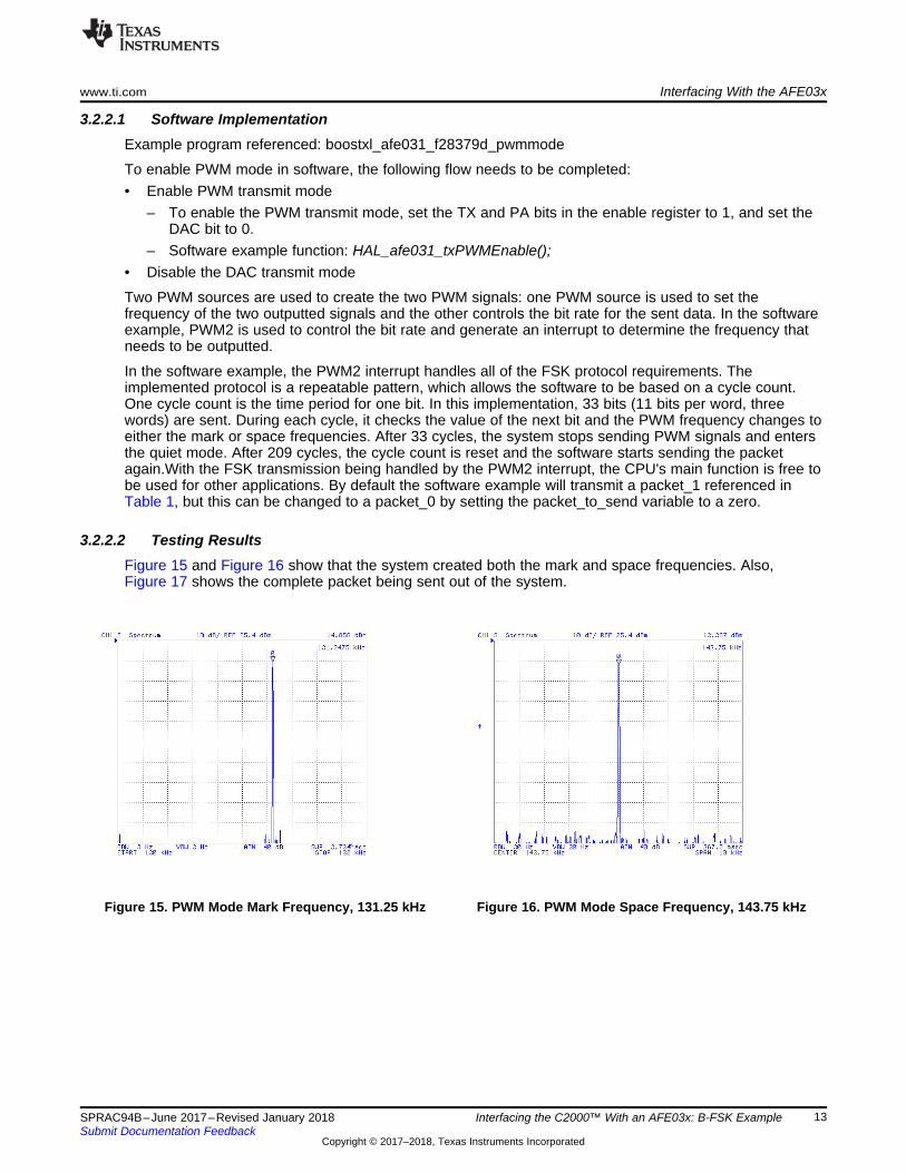
When using the transmitter solution in conjunction with the receiver solution, the complete systemconnection should look similar to what is shown in Figure 11.
Figure 11. TX-RX Solution System
3 Interfacing With the AFE03xWhen interfacing with the AFE03x as a transmitter, first decide which mode of operation to use for theAFE03x, DAC mode or PWM mode.
In DAC mode, the C2000 sends SPI data to update an internal DAC on the AFE031; the DAC valueoutput is filtered and amplified. In this mode, a sine table is cycled through, and each point is sent to theAFE031 over SPI.
In PWM mode, the SPI connection is only used to configure the registers for the AFE. Two PWM signalsare generated and supplied to the AFE031 at the desired frequency for FSK transmission. The AFE willadd these signals together to create a waveform that creates less harmonics than a single PWM signal.
Note that these two modes require different hardware configurations, so be sure to choose one or theother. If using the BOOSTXL-AFE031 test board as a reference, the hardware has been designed so thatboth modes can be used by simply adding or removing components.
When interfacing with the AFE03x as a receiver, the SPI connection is only used to set the registers of theAFE, much like the PWM transmit mode. The receive path of the AFE is enabled to allow the input signalto reach the ADC input of the C2000. Along this path lies some filters and two programmable-gainamplifiers (PGA) to step up or step down the input signal before entering the C2000 ADC.
3.1 Configuring the AFE031There are two main steps to configure the AFE device. First, ensure that the GPIOs are configuredcorrectly. On the AFE device, two main GPIOs are set up: DAC Mode Select and System Shutdown. Bothof these pins are pulled low. All other GPIOs connected can also be pulled low.
The next step is to configure the device over SPI. In the software example, the HAL_afe031Init() functionconfigures the AFE031 and is defined within AFE03x_Config.c.

Interfacing With the AFE03x www.ti.com
10 SPRAC94B–June 2017–Revised January 2018Submit Documentation Feedback
Copyright © 2017–2018, Texas Instruments Incorporated
Interfacing the C2000™ With an AFE03x: B-FSK Example
The steps below show the sequence the function follows to correctly configure the device:1. Configure GPIOs.
a. Setup SD and DAC pins on the AFE device. Both these pins need to be brought low.b. Software example function: HAL_afe031_cfgGpio();
2. Configure SPI.a. Configure SPI module for 16-bit characters. For more information regarding SPI requirements, see
the AFE031 Powerline Communications Analog Front-End Data Sheet .b. Software example function: HAL_spi_cfg();
3. Perform a soft reset on the AFE device.a. Write 0x14 to the reset register.b. Software example function: HAL_afe031_softReset();
4. Enable the Bias.a. Write 0x03 to the enable2 register.b. Software example function: HAL_afe031_biasEnable();
5. Select a Frequency Band.a. Write either 1 or 0 to the CA_CBCD bit inside the Control1 Register. If a 1 is written, the frequency
response of the TX and RX filters will be configured to CENELEC B,C,D. If a 0 is written, thenCENELEC A will be configured.
b. Software example function: HAL_afe031_bandSelect(1);6. Clear all interrupts
a. Write 0x00 to the control2 register.b. Software example function: HAL_afe031_clrAllInt();
7. Configure all interrupts.a. Interrupts can be configured by wrtiting to the control2 register. The software example function
currently only enables the T_flag that indicates thermal overload.b. Software example function: HAL_afe031_cfgInt();
8. Enable zc.a. Write a 1 to the ZC bit in the enable2 register.b. Software example function: HAL_afe031_zcEnable();
9. Write TX Gain - If Transmittinga. Write either a 0, 1, 2, or 3 to the TXG bits in the gain select register. The gains are as follows:
i. 0 =0.25 V/Vii. 1 = 0.5 V/Viii. 2 = 0.707 V/Viv. 3 = 1 V/V
b. Software example function: HAL_afe031_writeTxGain(UINT16 gain);i. Note that the software example function uses an array to write the 0-3. Thus when using the
function, the input parameter corresponds to the indice of the desired HAL_afe031_txGainLutarray element. For example passing 0 to the function corresponds to a gain of 0.25 V/V.
10. Write RX Gain - If Receiving.a. Write 0-15 to the RXG bits in the gain select register. The gains range from 0.25 V/V, when RXG is
set to 0x0, to 128 V/V, when RXG is set to 0xF.i. Refer to the Table 4 for specific gains.
b. Software example function: HAL_afe031_writeRxGain(UINT16 gain);i. Note that the software example function uses an array to write the 0-15. Thus, when using the
function, the input parameter corresponds to the indice of the desired HAL_afe031_rxGainLutarray element. The included array does not have values for all RX gain configurations.

www.ti.com Interfacing With the AFE03x
11SPRAC94B–June 2017–Revised January 2018Submit Documentation Feedback
Copyright © 2017–2018, Texas Instruments Incorporated
Interfacing the C2000™ With an AFE03x: B-FSK Example
Once the above is complete, begin the final few configurations needed based on the transmit or receiveimplementation being used.
3.2 Transmit PathNow that the AFE is initialized correctly, enable the system to transmit based on which transmit methodwas chosen: PWM Mode and DAC Mode.
3.2.1 FSK Example SpecificationsTable 1 describes the parameters around the FSK signal that is generated in the software example.
The end goal is to send the complete packet, wait the designated wait period, and repeat.
Table 1. FSK Specifications
Symbol TX Specification Min Nom Max Unit CommentW1 Logic 1 code word {{-1,-1,-1,+1,+1,+1,-1,+1,+1,-1,+1}} +1 = Mark, -1 =
SpaceW0 Logic 0 code word {{+1,+1,+1,-1,-1,-1,+1,-1,-1,+1,-1}} +1 = Mark, -1 =
Spacepacket_1 Complete Packet ABC = [W1,W1,W1]packet_0 Complete Packet ABC = [W0,W0,W0]Fm Mark Frequency 131.236875 131.25 131.263125 kHzFs Space Frequency 143.735625 143.75 143.764375 kHzTs Bit Period 5.119488 5.12 5.120512 msTt Tx Period 168.943104 168.96 168.976896 ms 3 wordsTq Quiet Period 901.029888 901.12 901.210112 ms 16 wordsTc Cycle Period 1069.972992 1070.08 1070.187008 ms 19 words
3.2.2 PWM ModeIn PWM mode, the C2000 F28379D generates two symmetric PWM signals that go directly into the AFEdevice. The two symmetric PWM signals are 66% and 33% duty cycle. These signals are added togetherinside the AFE device and create a waveform that has the least amount of noise. Figure 12 shows howthis addition works.
Figure 12. PWM Addition

PALPF PGA
C
Tx_PGA
_OUTPA_IN
PA_OUT1
PA_OUT2
C2000PWM Transmit Path Inside AFE031
43 kO
43 kO
Tx_F_OUT Tx_PGA
_OUT
C
C
510 Q�
510 Q�
GPIO
GPIO
Interfacing With the AFE03x www.ti.com
12 SPRAC94B–June 2017–Revised January 2018Submit Documentation Feedback
Copyright © 2017–2018, Texas Instruments Incorporated
Interfacing the C2000™ With an AFE03x: B-FSK Example
The path of the PWM signals is shown in Figure 13. The PWM signals go into the low-pass filter internalto the AFE030/1 device, and are added together to create the above PWM1+PWM2 waveform. The gainswitnessed at certain frequencies at the output of the internal TX low-pass filter are shown in Figure 14.
Figure 13. PWM Transmit Path
Figure 14. TX Filter Gain vs. Frequency
Next, the signal goes through a low-pass filter, PGA, another low-pass filter, and finally out of the PA. Theexternal low-pass filters can be tuned to filter the desired frequencies shown in Table 2.
Table 2. External R and C Values to Increase Filter Response in PWM Applications
Frequency Band R (Ω) C (nF)SFSK: 63 kHz, 74 kHz 510 2.7
CENELEC A 510 1.5CENELEC B,C,D 510 1
www.ti.com Interfacing With the AFE03x
13SPRAC94B–June 2017–Revised January 2018Submit Documentation Feedback
Copyright © 2017–2018, Texas Instruments Incorporated
Interfacing the C2000™ With an AFE03x: B-FSK Example
3.2.2.1 Software ImplementationExample program referenced: boostxl_afe031_f28379d_pwmmode
To enable PWM mode in software, the following flow needs to be completed:• Enable PWM transmit mode
– To enable the PWM transmit mode, set the TX and PA bits in the enable register to 1, and set theDAC bit to 0.
– Software example function: HAL_afe031_txPWMEnable();• Disable the DAC transmit mode
Two PWM sources are used to create the two PWM signals: one PWM source is used to set thefrequency of the two outputted signals and the other controls the bit rate for the sent data. In the softwareexample, PWM2 is used to control the bit rate and generate an interrupt to determine the frequency thatneeds to be outputted.
In the software example, the PWM2 interrupt handles all of the FSK protocol requirements. Theimplemented protocol is a repeatable pattern, which allows the software to be based on a cycle count.One cycle count is the time period for one bit. In this implementation, 33 bits (11 bits per word, threewords) are sent. During each cycle, it checks the value of the next bit and the PWM frequency changes toeither the mark or space frequencies. After 33 cycles, the system stops sending PWM signals and entersthe quiet mode. After 209 cycles, the cycle count is reset and the software starts sending the packetagain.With the FSK transmission being handled by the PWM2 interrupt, the CPU's main function is free tobe used for other applications. By default the software example will transmit a packet_1 referenced inTable 1, but this can be changed to a packet_0 by setting the packet_to_send variable to a zero.
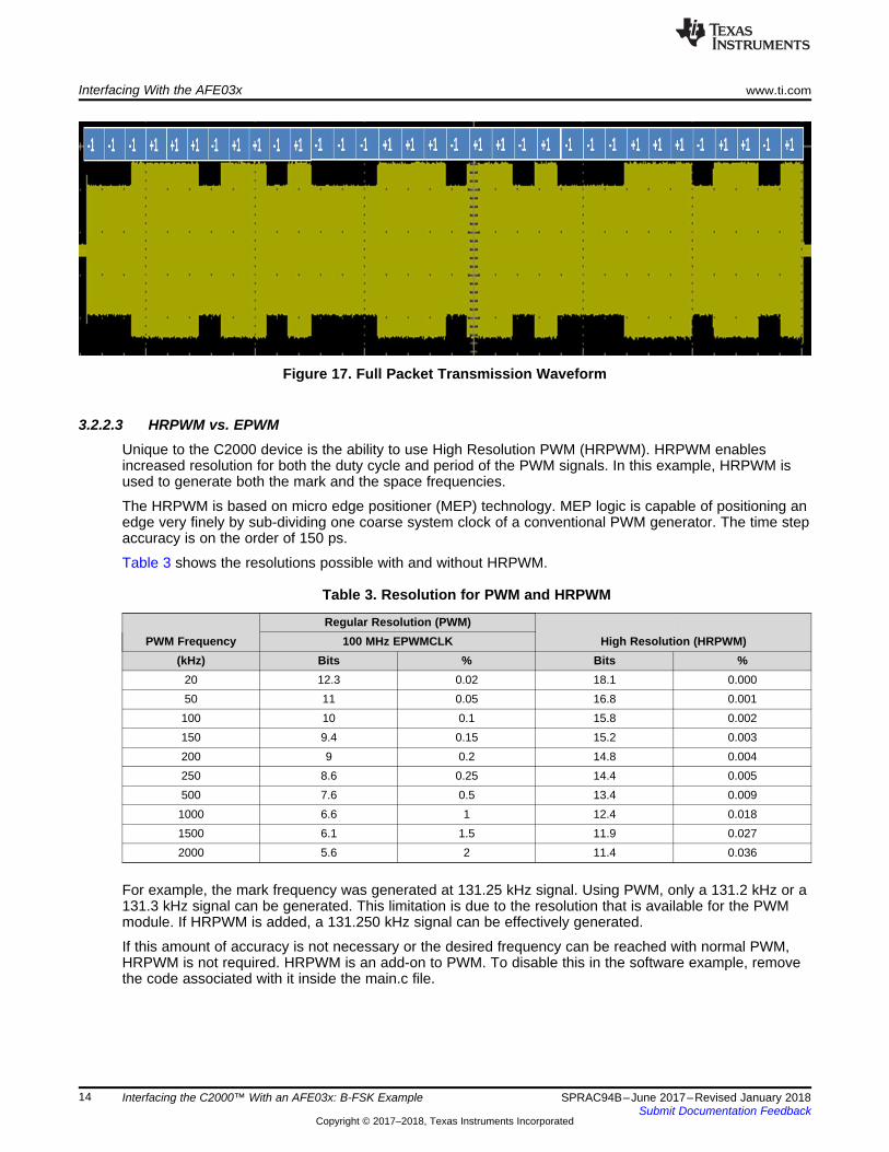
3.2.2.2 Testing ResultsFigure 15 and Figure 16 show that the system created both the mark and space frequencies. Also,Figure 17 shows the complete packet being sent out of the system.
Figure 15. PWM Mode Mark Frequency, 131.25 kHz Figure 16. PWM Mode Space Frequency, 143.75 kHz
Interfacing With the AFE03x www.ti.com
14 SPRAC94B–June 2017–Revised January 2018Submit Documentation Feedback
Copyright © 2017–2018, Texas Instruments Incorporated
Interfacing the C2000™ With an AFE03x: B-FSK Example
Figure 17. Full Packet Transmission Waveform
3.2.2.3 HRPWM vs. EPWMUnique to the C2000 device is the ability to use High Resolution PWM (HRPWM). HRPWM enablesincreased resolution for both the duty cycle and period of the PWM signals. In this example, HRPWM isused to generate both the mark and the space frequencies.
The HRPWM is based on micro edge positioner (MEP) technology. MEP logic is capable of positioning anedge very finely by sub-dividing one coarse system clock of a conventional PWM generator. The time stepaccuracy is on the order of 150 ps.
Table 3 shows the resolutions possible with and without HRPWM.
Table 3. Resolution for PWM and HRPWM
PWM FrequencyRegular Resolution (PWM)
High Resolution (HRPWM)100 MHz EPWMCLK(kHz) Bits % Bits %
20 12.3 0.02 18.1 0.00050 11 0.05 16.8 0.001100 10 0.1 15.8 0.002150 9.4 0.15 15.2 0.003200 9 0.2 14.8 0.004250 8.6 0.25 14.4 0.005500 7.6 0.5 13.4 0.0091000 6.6 1 12.4 0.0181500 6.1 1.5 11.9 0.0272000 5.6 2 11.4 0.036
For example, the mark frequency was generated at 131.25 kHz signal. Using PWM, only a 131.2 kHz or a131.3 kHz signal can be generated. This limitation is due to the resolution that is available for the PWMmodule. If HRPWM is added, a 131.250 kHz signal can be effectively generated.
If this amount of accuracy is not necessary or the desired frequency can be reached with normal PWM,HRPWM is not required. HRPWM is an add-on to PWM. To disable this in the software example, removethe code associated with it inside the main.c file.
www.ti.com Interfacing With the AFE03x
15SPRAC94B–June 2017–Revised January 2018Submit Documentation Feedback
Copyright © 2017–2018, Texas Instruments Incorporated
Interfacing the C2000™ With an AFE03x: B-FSK Example
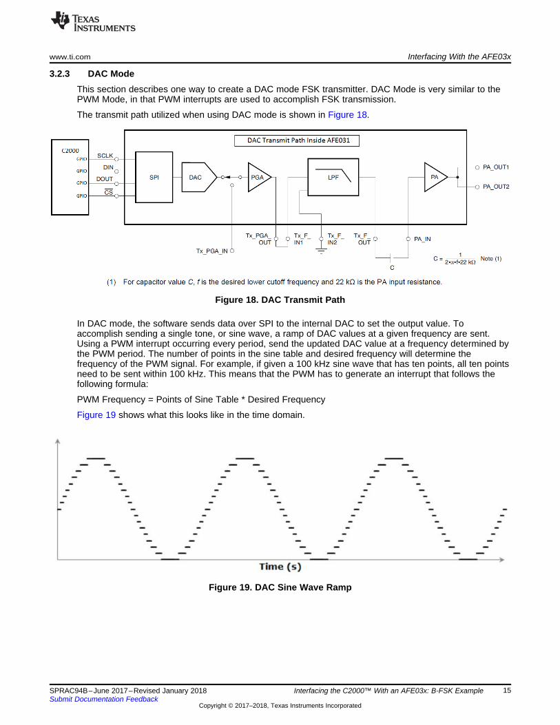
3.2.3 DAC ModeThis section describes one way to create a DAC mode FSK transmitter. DAC Mode is very similar to thePWM Mode, in that PWM interrupts are used to accomplish FSK transmission.
The transmit path utilized when using DAC mode is shown in Figure 18.
Figure 18. DAC Transmit Path
In DAC mode, the software sends data over SPI to the internal DAC to set the output value. Toaccomplish sending a single tone, or sine wave, a ramp of DAC values at a given frequency are sent.Using a PWM interrupt occurring every period, send the updated DAC value at a frequency determined bythe PWM period. The number of points in the sine table and desired frequency will determine thefrequency of the PWM signal. For example, if given a 100 kHz sine wave that has ten points, all ten pointsneed to be sent within 100 kHz. This means that the PWM has to generate an interrupt that follows thefollowing formula:
PWM Frequency = Points of Sine Table * Desired Frequency
Figure 19 shows what this looks like in the time domain.
Figure 19. DAC Sine Wave Ramp

Interfacing With the AFE03x www.ti.com
16 SPRAC94B–June 2017–Revised January 2018Submit Documentation Feedback
Copyright © 2017–2018, Texas Instruments Incorporated
Interfacing the C2000™ With an AFE03x: B-FSK Example
3.2.3.1 Software ImplementationExample program referenced: boostxl_afe031_f28379d_dacmode
To enable DAC mode in software, the following flow needs to be completed• Enable DAC transmit mode internal to AFE.
– To enable the PWM transmit mode, set the TX and PA bits in the enable register to 1, and set theDAC bit to 0.
– Software example function: HAL_afe031_txDACEnable();• Enable the DAC transmit mode with GPIO toggle and Configure word length for SPI
– Set the GPIO connected the the DAC pin to 1.– set word length to 10 bytes for SPI communication.– Software example function: HAL_afe031_dacEnable();
Sending information in DAC mode, can be accomplished very similarly to how the PWM mode operates.One PWM source is used to set the DAC mode value to the correct value of the sine ramp that gets sentout. The second PWM is used for bit rate to generate an interrupt and determine what frequency needs tobe outputted.
A problem does arise if attempting to reach vary precise frequencies with this implementation. Theproblem can be looked at with Equation 1.Number of steps in Sine Table = (Frequency of Interrupt) / (Frequency of Desired Signals) (1)
If trying to generate 131.25 kHz, then only two variables can change. One approach is to set the numberof steps in the sine table. For example, if there are 10 steps in the sine table the Frequency of interrupt is:
Frequency of Interrupt = (Number of Steps in Sine Table) * (Frequency of Desired Signal)
Frequency of Interrupt = 1.3125 MHz
With a 200 MHz clock,even if an interrupt occurs at either 152 or 153 CPU cycles, the interruptfrequencies would be 1.31579 MHz and 1.30719 MHz respectively. These frequencies do not fall withinspec for the frequency tolerances in Table 1. This means setting the step size cannot be the correctimplementation for precise frequency generation.
The other way to think of this is to set the frequency of interrupt. Let's set the interrupt for 1 MHz,something that is possible to generate. The number of steps in the sine wave would then be:
Number of steps in Sine Table = (1 MHz) / (131.25 kHz)
Number of Steps in sine Table = 7.61905
Utlizing the floating-point capability of the F28379D, the processor can keep track of that remainder, andnow the accuracy depends on the sine table, not the 1 MHz clock. The step size can be found using thefollowing formula:
Step Size = (Points in Sine Table)/ (Number of steps in Sine Table)
With a 4096 sine table, and continuing with the previous example, this gives 537.6 as the step size. Thismeans in every interrupt, the sine table will step another 537.6. Since the program is sorting through anarray, this number will be rounded off to 537, but as this number gets added and the program shiftsthrough the sine table, the next step will vary off the decimal step size. An example interrupt routine isshown below:• //Transmit next data point in sine wave. Also convert float SinePosition to unsigned int
– Uint16 temp = sinePosition;– HAL_spi_xmt((sineTable[temp]) );
• //Calculate next step– sinePosition += sineStep; }
• //Check for overflow– if(sinePosition > 4095)– { sinePosition -= 4095; }

www.ti.com Interfacing With the AFE03x
17SPRAC94B–June 2017–Revised January 2018Submit Documentation Feedback
Copyright © 2017–2018, Texas Instruments Incorporated
Interfacing the C2000™ With an AFE03x: B-FSK Example
One aspect to note is that in this implementation, a 1 MHz Interrupt was created, which only moves datafrom one memory address to another. A way to make this less CPU intensive is to utilize the C2000'sDMA (Direct Memory Access). The DMA peripheral moves data from one memory address to anotherbased on a trigger event. Pre-fill two buffers with the correct data that is chosen to send out over SPI, anduse the DMA to switch between the two. When switching from one buffer to the other, the older buffer willrefill with the values.
In the DAC Mode software, a 1 MHz PWM signal is utilized to generate a DMA event that moves datafrom one of these buffers to the SPI TX Buffer. Since the older buffer needs to be re-filled after each use,the DMA will trigger an event each time it finishes reading an entire buffer. During this interrupt, thebuffers are switched, and the old one is re-filled. By following this implementation, CPU utilization vs.memory tradeoffs can be weighed and the buffers can be sized accordingly. If extra memory is available,using a bigger buffer will reduce the CPU overhead. If not a lot of memory is available, then the smallerthe buffer size increases the CPU overhead.
Exactly like the PWM mode software implementation, the PWM2 interrupt handles all of the FSK protocolneeds. The protocol being implemented is a repeatable pattern, which allows the software to be based ona cycle count. One cycle count is the time period for one bit. In this implementation, 33 bits (11 bits perword, three words) are being sent. During each cycle, a check to see the value of the next bit and the stepsize changes to allow the sine table to be sent out at the mark or space frequencies. After 33 cycles, thesystem stops sending DAC values and enters the quiet mode. After 209 cycles, the cycle count is resetand the software starts sending the packet again.With the FSK transmission being handled by the PWM2interrupt, the CPU's main function is free to be used for other applications. By default the softwareexample will transmit a packet_1 referenced in Table 1, but this can be changed to a packet_0 by settingthe packet_to_send variable to a zero.
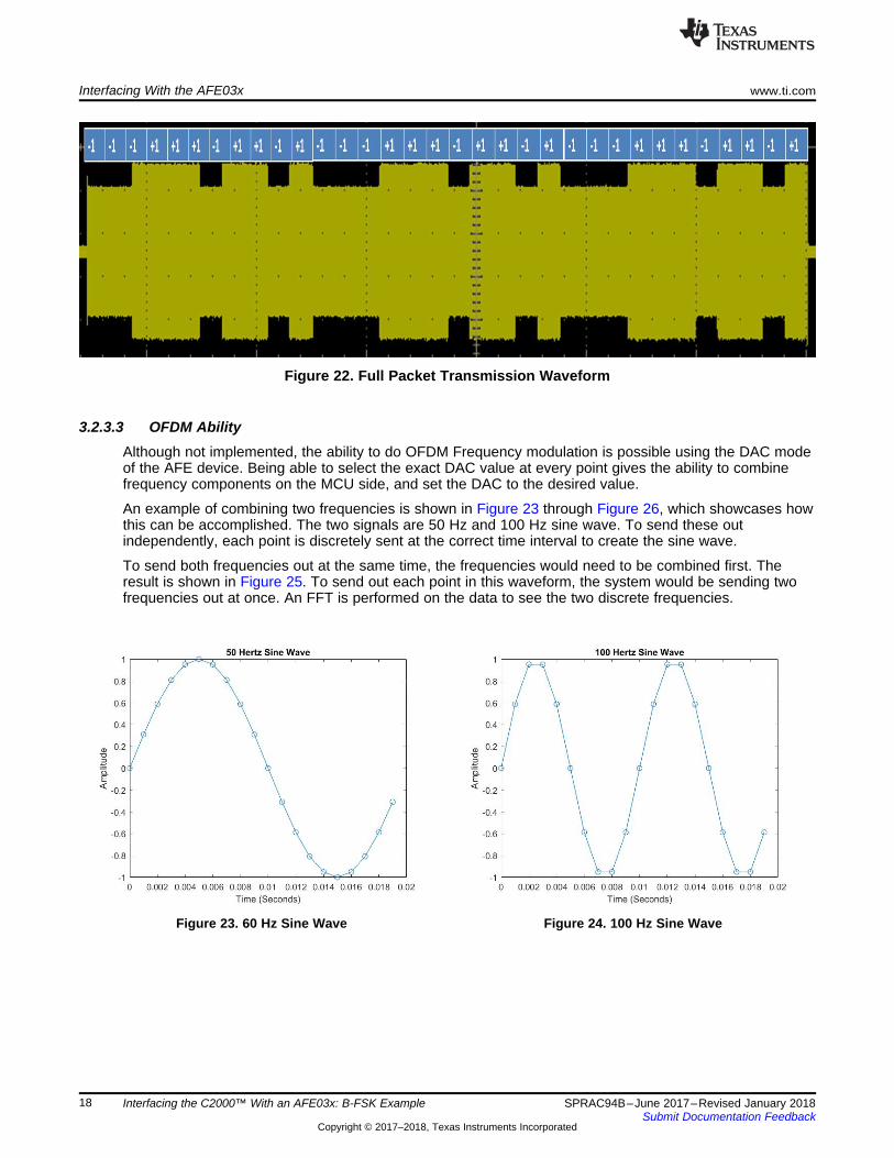
3.2.3.2 Testing ResultsFigure 20 and Figure 21 show that the system created both the mark and space frequencies. Also,Figure 22 shows the complete packet being sent out of the system.
Figure 20. DAC Mode Mark Frequency SpectrumAnalyzer
Figure 21. DAC Mode Space Frequency SpectrumAnalyzer
Interfacing With the AFE03x www.ti.com
18 SPRAC94B–June 2017–Revised January 2018Submit Documentation Feedback
Copyright © 2017–2018, Texas Instruments Incorporated
Interfacing the C2000™ With an AFE03x: B-FSK Example
Figure 22. Full Packet Transmission Waveform
3.2.3.3 OFDM AbilityAlthough not implemented, the ability to do OFDM Frequency modulation is possible using the DAC modeof the AFE device. Being able to select the exact DAC value at every point gives the ability to combinefrequency components on the MCU side, and set the DAC to the desired value.
An example of combining two frequencies is shown in Figure 23 through Figure 26, which showcases howthis can be accomplished. The two signals are 50 Hz and 100 Hz sine wave. To send these outindependently, each point is discretely sent at the correct time interval to create the sine wave.
To send both frequencies out at the same time, the frequencies would need to be combined first. Theresult is shown in Figure 25. To send out each point in this waveform, the system would be sending twofrequencies out at once. An FFT is performed on the data to see the two discrete frequencies.
Figure 23. 60 Hz Sine Wave Figure 24. 100 Hz Sine Wave

PGA2
C2000
ADC
Phase
Neutral
N1 N2
+ +
R2C2L2
R1 L1C1
PGA1
LPFC
Inside AFE031 Receive Path
www.ti.com Interfacing With the AFE03x
19SPRAC94B–June 2017–Revised January 2018Submit Documentation Feedback
Copyright © 2017–2018, Texas Instruments Incorporated
Interfacing the C2000™ With an AFE03x: B-FSK Example
Figure 25. 60 + 100 Hz Sine Wave Figure 26. FFT of Combined Signals
3.3 Receive PathThe C2000 AFE031 interface can also be used as a FSK receiver to translate the transmitted frequencyshifted signal into digital data. This section describes one way to create a FSK receiver using the C2000AFE031 interface.
3.3.1 Receive Path OverviewThe C2000 AFE031 system receive path is shown in Figure 27. There is a significant amount of filteringthe input signal must traverse along the path from the transformer on the right to the input of the C2000ADC on the left. On the AFE side, the AFE031 has vast filtering abilities for these signals.
Figure 27. AFE031 Receive Path Interfaced With C2000 ADC
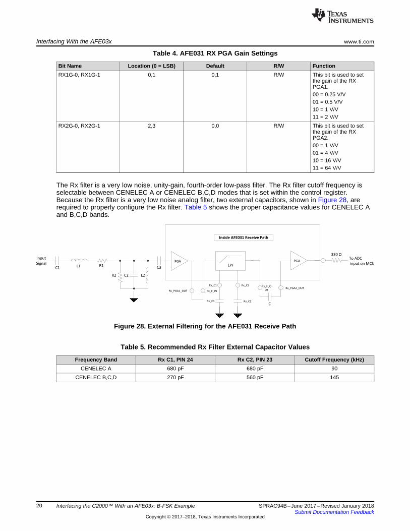
The AFE031 RX path consists of Rx PGA1, the Rx Low Pass Filter, and Rx PGA2. Both Rx PGA1 and RxPGA2 are high performance programmable gain amplifiers that can be configured through SPI. Rx PGA1can operate as either an attenuator, providing loss, or an amplfier, providing gain. The gain steps of theRx PGA1 are 0.25 V/V, 0.5 V/V, 1 V/V, and 2 V/V. The gain steps of the Rx PGA2 are 1 V/V, 4 V/V, 16V/V, and 64 V/V. For specific RX PGA Gain Select Register values, see Table 4. Configuring the RxPGA1 as an attenuator (at gains less than 1 V/V) is useful for applications where the presence of largeinterference signals are present within the signal band. Attenuating the large interference allows thesesignals to pass through the analog Rx signal chain without causing an overload; the interference signalcan then be processed and removed within the microcontroller, as necessary.
PGA
R2 C2 L2
R1L1C1
PGA
LPFC3
Inside AFE031 Receive Path
330 O
Rx_PGA1_OUT Rx_F_IN
Rx_C1 Rx_C2
Rx_C1 Rx_C2
Rx_PGA2_OUTRx_F_O
UT
To ADC
input on MCU
C
Input
Signal
Interfacing With the AFE03x www.ti.com
20 SPRAC94B–June 2017–Revised January 2018Submit Documentation Feedback
Copyright © 2017–2018, Texas Instruments Incorporated
Interfacing the C2000™ With an AFE03x: B-FSK Example
Table 4. AFE031 RX PGA Gain Settings
Bit Name Location (0 = LSB) Default R/W FunctionRX1G-0, RX1G-1 0,1 0,1 R/W This bit is used to set
the gain of the RXPGA1.00 = 0.25 V/V01 = 0.5 V/V10 = 1 V/V11 = 2 V/V
RX2G-0, RX2G-1 2,3 0,0 R/W This bit is used to setthe gain of the RXPGA2.00 = 1 V/V01 = 4 V/V10 = 16 V/V11 = 64 V/V
The Rx filter is a very low noise, unity-gain, fourth-order low-pass filter. The Rx filter cutoff frequency isselectable between CENELEC A or CENELEC B,C,D modes that is set within the control register.Because the Rx filter is a very low noise analog filter, two external capacitors, shown in Figure 28, arerequired to properly configure the Rx filter. Table 5 shows the proper capacitance values for CENELEC Aand B,C,D bands.
Figure 28. External Filtering for the AFE031 Receive Path
Table 5. Recommended Rx Filter External Capacitor Values
Frequency Band Rx C1, PIN 24 Rx C2, PIN 23 Cutoff Frequency (kHz)CENELEC A 680 pF 680 pF 90
CENELEC B,C,D 270 pF 560 pF 145
www.ti.com Interfacing With the AFE03x
21SPRAC94B–June 2017–Revised January 2018Submit Documentation Feedback
Copyright © 2017–2018, Texas Instruments Incorporated
Interfacing the C2000™ With an AFE03x: B-FSK Example
Capacitor Rx C1 is connected between pin 24 and ground, and Rx C2 is connected between pin 23 andground. For the capacitors shown, it is recommended that these components be rated to withstand the fullAVDD power-supply voltage.
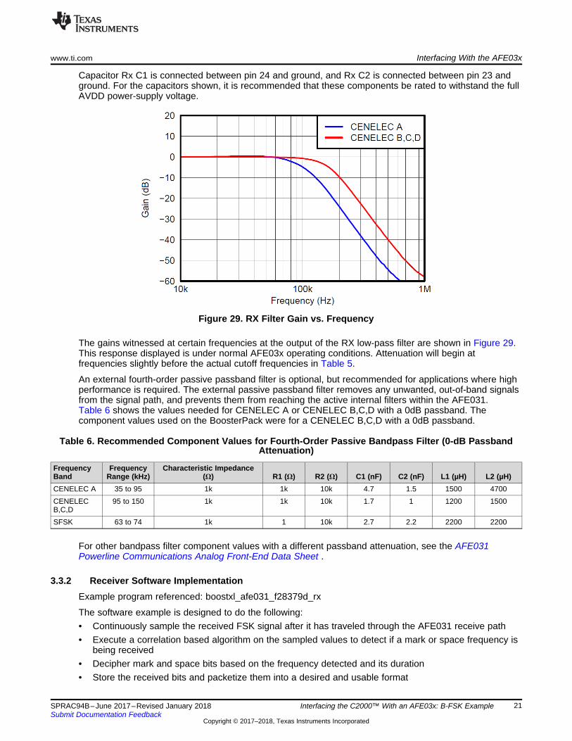
Figure 29. RX Filter Gain vs. Frequency
The gains witnessed at certain frequencies at the output of the RX low-pass filter are shown in Figure 29.This response displayed is under normal AFE03x operating conditions. Attenuation will begin atfrequencies slightly before the actual cutoff frequencies in Table 5.
An external fourth-order passive passband filter is optional, but recommended for applications where highperformance is required. The external passive passband filter removes any unwanted, out-of-band signalsfrom the signal path, and prevents them from reaching the active internal filters within the AFE031.Table 6 shows the values needed for CENELEC A or CENELEC B,C,D with a 0dB passband. Thecomponent values used on the BoosterPack were for a CENELEC B,C,D with a 0dB passband.
Table 6. Recommended Component Values for Fourth-Order Passive Bandpass Filter (0-dB PassbandAttenuation)
FrequencyBand
FrequencyRange (kHz)
Characteristic Impedance(Ω) R1 (Ω) R2 (Ω) C1 (nF) C2 (nF) L1 (µH) L2 (µH)
CENELEC A 35 to 95 1k 1k 10k 4.7 1.5 1500 4700CENELECB,C,D
95 to 150 1k 1k 10k 1.7 1 1200 1500
SFSK 63 to 74 1k 1 10k 2.7 2.2 2200 2200
For other bandpass filter component values with a different passband attenuation, see the AFE031Powerline Communications Analog Front-End Data Sheet .
3.3.2 Receiver Software ImplementationExample program referenced: boostxl_afe031_f28379d_rx
The software example is designed to do the following:• Continuously sample the received FSK signal after it has traveled through the AFE031 receive path• Execute a correlation based algorithm on the sampled values to detect if a mark or space frequency is
being received• Decipher mark and space bits based on the frequency detected and its duration• Store the received bits and packetize them into a desired and usable format

Interfacing With the AFE03x www.ti.com
22 SPRAC94B–June 2017–Revised January 2018Submit Documentation Feedback
Copyright © 2017–2018, Texas Instruments Incorporated
Interfacing the C2000™ With an AFE03x: B-FSK Example
To enable the system to receive in software, the following needs to be completed• The RX bit in the enable register must be set to 1 to open the AFE031 receive path.
– Software example function: HAL_afe031_rxEnable();• Include the fsk_corr_detect library and related header files in the project:
– fsk_corr_detect.lib– fsk_corr_detector.h– fsk_packetization.h
3.3.2.1 Initial Setup and ParametersThe FSK signals being received follow a set of communication parameters that must be designed aroundwithin software.
Figure 30. Received FSK Signal
The communication parameters of interest are illustrated in Figure 30. The labeled parameters representthe following:• Tbit : Bit Period• Fbit : Bit Frequency• Fmark : Mark Frequency• Fspace : Space Frequency• TS : Sampling Period• FS : Sampling Frequency
For the example program the communication parameters being followed by default are stated in Table 1.Create a FSK_CORR_DETECTOR structure, declared in fsk_corr_detector.h, to hold the parametersnecessary for accurate receiving.
volatile FSK_CORR_DETECTOR FSK_struct1; // FSK structure
The example software and fsk_corr_detect library are designed to detect a set of user specifiedfrequencies, one mark frequency and one space frequency. These frequencies will have to be within thefrequency band ranges of the AFE031's CENELEC A or CENELEC B,C,D configurations. The exampleprogram utilizes a mark frequency of 131.25 kHz and a space frequency of 143.75 kHz and is meant to beused with the CENELEC B,C,D configuration. Set the mark_freq and space_freq members of theFSK_CORR_DETECTOR structure with these frequencies.
FSK_struct1.mark_freq = 131250; // Mark Frequency DetectedFSK_struct1.space_freq = 143750; // Space Frequency Detected

www.ti.com Interfacing With the AFE03x
23SPRAC94B–June 2017–Revised January 2018Submit Documentation Feedback
Copyright © 2017–2018, Texas Instruments Incorporated
Interfacing the C2000™ With an AFE03x: B-FSK Example
The C2000's ADC is used to sample the FSK input signal. The sampling frequency, FS, must follow theNyquist theorem; the input signal must be sampled at a rate of at least 2x the highest signal frequencytrying to be detected. That is, if the highest signal frequency to be detected is 100 kHz, FS must be at least200 kHz. In the example program the highest freqeuncy being detected is a 143.75 kHz space frequencyand the sampling rate is set to 300 kHz, which is more than the required rate. Set the isr_freq member ofthe FSK_CORR_DETECTOR structure to the acceptable FS.
FSK_struct1.isr_freq = 300000; // ADC Sampling frequency
A bit decision algorithm is intended to be run at three times the bit frequency. For example, if each bitperiod is 1 ms long, the bit frequency is 1 kHz making the desired bit decision frequency 3 kHz. Theexample program is detecting bits with a period of 5.12 ms making the bit frequency 195.3125 Hz and thedesired bit decision frequency 585.9375 Hz. The bit decision frequency in software should be as close aspossible to the desired frequency to prevent bit boundary issues. Set the bit_freq member of theFSK_CORR_DETECTOR structure with this bit decision frequency.
FSK_struct1.bit_freq = 586; // Bit decision frequency, 3x bit frequency
In summary, the frequency parameters set for the example program are shown in Table 7.
Table 7. Software Frequency Parameters
Parameter FrequencyDetected Mark Frequency 131.25 kHzDetected Space Frequency 143.75 kHzInput Signal Sampling Frequency 300 kHzBit Decision Algorithm Frequency 586 Hz (rounded up)
Set the detection_threshold member of the FSK_CORR_DETECTOR structure. This value plays a role intuning the bit detection senstivity.
#define FSK_BIT_DETECTION_THRESHOLD 0.1 // Bit detection threshold valueFSK_struct1.detection_threshold = FSK_BIT_DETECTION_THRESHOLD; // Set threshold
Complete the fsk_corr_detect library's initialization based on the member values inputted by calling thecorresponding init function.
FSK_CORR_DETECTOR_INIT(&FSK_struct1); // Initialize FSK structure
Additionally, the format of received information is taken into account by setting the following parameterswithin software.• The number of bits that make up a word, #define within fsk_packetization.h:
– #define NUMBER_OF_BITS_PER_WORD 11• The number of words that make up a packet, #define within fsk_packetization.h:
– #define NUMBER_OF_WORDS 3• The number of total bits within a packet, #define within fsk_corr_detector.h:
– #define RX_MESSAGE_SIZE 33
3.3.2.2 Interrupt Service RoutinesISRs running at these predetermined frequencies carry out the main functions of the receiver solution. Theexample program makes use of the C2000's EPwms and CPU timer to trigger necessary interrupts.
An ADC sampling ISR, configured using EPwm1, is set to trigger at the 300 kHz input signal samplingfrequency. The ISR function samples the ADC, scales the sampled value, and passes the scaled value toa library function for signal processing.

Interfacing With the AFE03x www.ti.com
24 SPRAC94B–June 2017–Revised January 2018Submit Documentation Feedback
Copyright © 2017–2018, Texas Instruments Incorporated
Interfacing the C2000™ With an AFE03x: B-FSK Example
A bit-decision ISR, configured using EPwm2, is set to trigger at 585.92 Hz. This frequency is as close tothe desired 585.9375 Hz the EPwm module could achieve. The ISR function takes the signal processingwork of the previous ADC sampling ISR and checks if a mark or space bit has been detected. If a mark orspace bit is detected then the detected bit is placed into a received message buffer. Once the messagebuffer is full, a flag will be set to signify a full packet has been received.
A message timeout ISR, configured using CPU timer 2, is set to trigger if the user specified time limit isreached while receiving. By default this time limit is set to 3 seconds by the RX_MESSAGE_TIMEOUT#define. The timer begins right before the system starts receiving and will reset if a packet is received. If apacket is not received within the specified time limit, the ISR triggers and causes the system to stopreceiving.
3.3.2.3 Run Time OperationDuring run time the receiver operates in the following way:1. The system will begins to continuously receive incoming data by starting the EPwms and CPU timer to
trigger interrupts.a. Example Program Function: Start_Receiving();
2. The ISRs will run until the full packet of data is received or the specified timeout is reached.a. The rxMessage[] buffer will be filled with the received bits while the ISRs are running
3. Once the packet of data is received or the specified timeout is reached, the system will stop receivingdata to reduce CPU utilization during quiet periods.a. Example Program Function: Stop_Receiving();b. The function stops the EPwms and stops and resets the CPU timer
4. The received data is then packetized into the desired format.a. Example Program Function: Packetize(int message[], int packet[]);b. The function takes the rxMessage[] buffer containing 33 received bits and fills the packet[] buffer
with three, 11 bit, words by summing up the received bits for each word. The rxMessage[] buffercontents are then set to zero.i. +1 equates to a W1 following the specs in Table 1ii. -1 equates to a W0 following the specs in Table 1
c. The function sums up the values of the packet[] and saves the sum to the packet_sum variablea. +3 equates to a packet_1 following the specs in Table 1b. -3 equates to a packet_0 following the specs in Table 1
5. The packetized data is used before the receive process restarts.a. Example Program Function: Visual_Indication();b. The function causes the LEDs on the BOOSTXL-AFE031 to blink accordingly
i. Blue LED blinks if a packet_1 was receivedii. Red LED blinks if a packet_0 was receivediii. Red and Blue LEDs blink if neither a packet_1 or packet_0 were received, or if a timeout
occurs
www.ti.com Interfacing With the AFE03x
25SPRAC94B–June 2017–Revised January 2018Submit Documentation Feedback
Copyright © 2017–2018, Texas Instruments Incorporated
Interfacing the C2000™ With an AFE03x: B-FSK Example
3.3.2.4 Testing ResultsThe performance of the FSK receiver solution was tested in a controlled lab environment using either thePWM or DAC mode transmitter solution to provide the input FSK signal. The established setup is similar towhat is shown in Figure 11 without any coupling circuitry. The purpose of the tests were to confirm that thereceiver solution could effectively translate a received FSK signal into the original digital information.
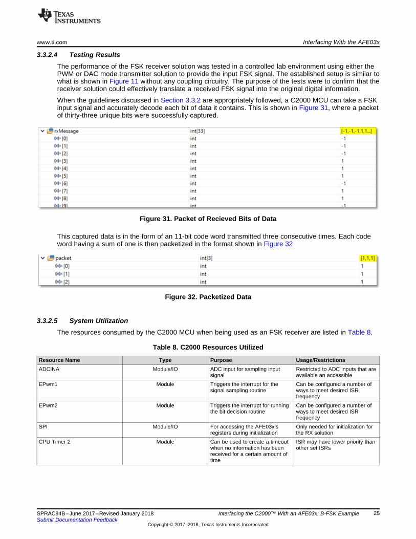
When the guidelines discussed in Section 3.3.2 are appropriately followed, a C2000 MCU can take a FSKinput signal and accurately decode each bit of data it contains. This is shown in Figure 31, where a packetof thirty-three unique bits were successfully captured.
Figure 31. Packet of Recieved Bits of Data
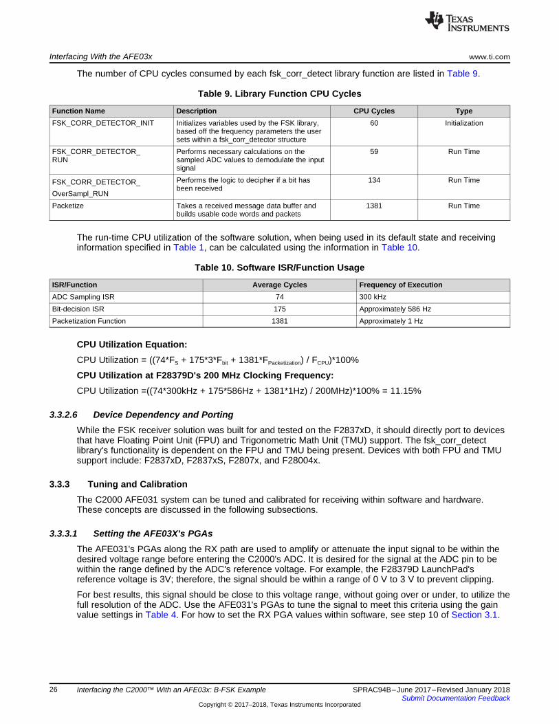
This captured data is in the form of an 11-bit code word transmitted three consecutive times. Each codeword having a sum of one is then packetized in the format shown in Figure 32
Figure 32. Packetized Data
3.3.2.5 System UtilizationThe resources consumed by the C2000 MCU when being used as an FSK receiver are listed in Table 8.
Table 8. C2000 Resources Utilized
Resource Name Type Purpose Usage/RestrictionsADCINA Module/IO ADC input for sampling input
signalRestricted to ADC inputs that areavailable an accessible
EPwm1 Module Triggers the interrupt for thesignal sampling routine
Can be configured a number ofways to meet desired ISRfrequency
EPwm2 Module Triggers the interrupt for runningthe bit decision routine
Can be configured a number ofways to meet desired ISRfrequency
SPI Module/IO For accessing the AFE03x’sregisters during initialization
Only needed for initialization forthe RX solution
CPU Timer 2 Module Can be used to create a timeoutwhen no information has beenreceived for a certain amount oftime
ISR may have lower priority thanother set ISRs
Interfacing With the AFE03x www.ti.com
26 SPRAC94B–June 2017–Revised January 2018Submit Documentation Feedback
Copyright © 2017–2018, Texas Instruments Incorporated
Interfacing the C2000™ With an AFE03x: B-FSK Example
The number of CPU cycles consumed by each fsk_corr_detect library function are listed in Table 9.
Table 9. Library Function CPU Cycles
Function Name Description CPU Cycles TypeFSK_CORR_DETECTOR_INIT Initializes variables used by the FSK library,
based off the frequency parameters the usersets within a fsk_corr_detector structure
60 Initialization
FSK_CORR_DETECTOR_RUN
Performs necessary calculations on thesampled ADC values to demodulate the inputsignal
59 Run Time
FSK_CORR_DETECTOR_OverSampl_RUN
Performs the logic to decipher if a bit hasbeen received
134 Run Time
Packetize Takes a received message data buffer andbuilds usable code words and packets
1381 Run Time
The run-time CPU utilization of the software solution, when being used in its default state and receivinginformation specified in Table 1, can be calculated using the information in Table 10.
Table 10. Software ISR/Function Usage
ISR/Function Average Cycles Frequency of ExecutionADC Sampling ISR 74 300 kHzBit-decision ISR 175 Approximately 586 HzPacketization Function 1381 Approximately 1 Hz
CPU Utilization Equation:CPU Utilization = ((74*FS + 175*3*Fbit + 1381*FPacketization) / FCPU)*100%
CPU Utilization at F28379D's 200 MHz Clocking Frequency:CPU Utilization =((74*300kHz + 175*586Hz + 1381*1Hz) / 200MHz)*100% = 11.15%
3.3.2.6 Device Dependency and PortingWhile the FSK receiver solution was built for and tested on the F2837xD, it should directly port to devicesthat have Floating Point Unit (FPU) and Trigonometric Math Unit (TMU) support. The fsk_corr_detectlibrary's functionality is dependent on the FPU and TMU being present. Devices with both FPU and TMUsupport include: F2837xD, F2837xS, F2807x, and F28004x.
3.3.3 Tuning and CalibrationThe C2000 AFE031 system can be tuned and calibrated for receiving within software and hardware.These concepts are discussed in the following subsections.
3.3.3.1 Setting the AFE03X's PGAsThe AFE031's PGAs along the RX path are used to amplify or attenuate the input signal to be within thedesired voltage range before entering the C2000's ADC. It is desired for the signal at the ADC pin to bewithin the range defined by the ADC's reference voltage. For example, the F28379D LaunchPad'sreference voltage is 3V; therefore, the signal should be within a range of 0 V to 3 V to prevent clipping.
For best results, this signal should be close to this voltage range, without going over or under, to utilize thefull resolution of the ADC. Use the AFE031's PGAs to tune the signal to meet this criteria using the gainvalue settings in Table 4. For how to set the RX PGA values within software, see step 10 of Section 3.1.
www.ti.com Interfacing With a Power Line
27SPRAC94B–June 2017–Revised January 2018Submit Documentation Feedback
Copyright © 2017–2018, Texas Instruments Incorporated
Interfacing the C2000™ With an AFE03x: B-FSK Example
3.3.3.2 Automatic Gain Control (AGC)If the receiver system is to be used within an application that has an input signal with inconsistentamplitudes, it may be necessary to implement some form of Automatic Gain Control (AGC) to manage thesignal before it reaches the C2000's ADC input. The AGC would be a closed-loop feedback system thatmeasures the amplitude of the input signal, or a related response, and based on what is observed amplifyor attenuate the signal.
The AFE031's internal PGAs could be leveraged to dynamically amplify or attenuate the signal to be withinthe desired amplitude range. For gain select times of the two PGAs along the RX path, see the AFE031Datasheet .
Another approach would be to perform the AGC externally before the signal enters the C2000/AFE031system. However, this requires additional circuitry involving a variable gain amplifier (VGA) to be added.
3.3.3.3 Setting the Bit Detection ThresholdThe detection_threshold member of the FSK_CORR_DETECTOR structure, mentioned in Section 3.3.2.1,is in direct relation to the accuracy of bit detections. The threshold needs to be set to a value between 0and 1. If set to a value too high then bits will not be detected at all, but if set too low then there could beconfusion as to what constitutes a mark or space bit and cause bit errors. It may take some trial and errorto find a value that consistently detects bits without errors.
3.3.3.4 FSK Correlation Detector LibraryFor inquiries related to the FSK correlation detector library utilized in the software example, email thefollowing address: [email protected].
To request access to the library’s source code (contingent on end application review and export controlapproval from Texas Instruments Incorporated), follow the instructions at the following url:https://www.ti.com/licreg/docs/swlicexportcontrol.tsp?form_id=268791&prod_no=C2000-AFE031_FSK_RX_SOURCE&ref_url=c2000.
4 Interfacing With a Power LinePower Line Communication (PLC) is utilized with Texas Instruments C2000 paired with the AFE031device, which enables data to be sent over existing power cables. This means that one can both powerand control/retrieve data at the same time with just power cables running though these devices. Thisminimizes the overall cost that would be needed otherwise to create a communications path with extracabling.
4.1 Line CouplingLine coupling is one of the most crucial segments of the PLC system having two primary functions. Thefirst function is to couple the signal from the AFE031 to and from the ac mains/dc Buss. The second is toprevent the low frequency high voltage of 50/60 Hz from the mains from damaging the PLC circuitry.
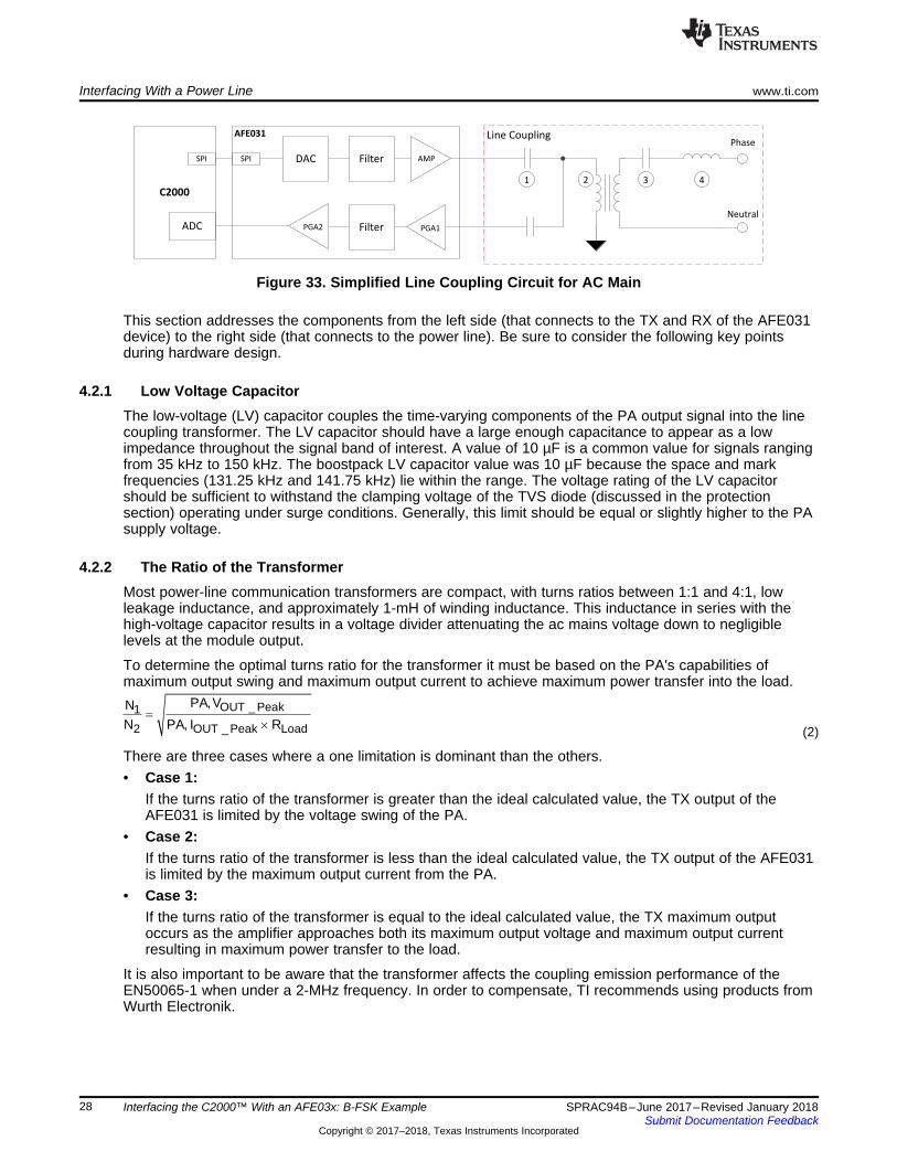
4.2 Coupling to an AC LineFor coupling to the ac main, the following components are needed: low-voltage capacitor, transformer,high-voltage capacitor, and an inductor. It is important to note that this section does not show thenecessary protection circuitry; that information is discussed in Section 4.4 . A simplified diagram is shownFigure 33.
_1
2 _
,
,OUT Peak
OUT Peak Load
PA VNN PA I R
u
Line Coupling
FilterPGA2
AMPFilterDAC
C2000
SPI
ADC
SPI
Phase
Neutral
PGA1
1 2 3 4
AFE031
Interfacing With a Power Line www.ti.com
28 SPRAC94B–June 2017–Revised January 2018Submit Documentation Feedback
Copyright © 2017–2018, Texas Instruments Incorporated
Interfacing the C2000™ With an AFE03x: B-FSK Example
Figure 33. Simplified Line Coupling Circuit for AC Main
This section addresses the components from the left side (that connects to the TX and RX of the AFE031device) to the right side (that connects to the power line). Be sure to consider the following key pointsduring hardware design.
4.2.1 Low Voltage CapacitorThe low-voltage (LV) capacitor couples the time-varying components of the PA output signal into the linecoupling transformer. The LV capacitor should have a large enough capacitance to appear as a lowimpedance throughout the signal band of interest. A value of 10 µF is a common value for signals rangingfrom 35 kHz to 150 kHz. The boostpack LV capacitor value was 10 µF because the space and markfrequencies (131.25 kHz and 141.75 kHz) lie within the range. The voltage rating of the LV capacitorshould be sufficient to withstand the clamping voltage of the TVS diode (discussed in the protectionsection) operating under surge conditions. Generally, this limit should be equal or slightly higher to the PAsupply voltage.
4.2.2 The Ratio of the TransformerMost power-line communication transformers are compact, with turns ratios between 1:1 and 4:1, lowleakage inductance, and approximately 1-mH of winding inductance. This inductance in series with thehigh-voltage capacitor results in a voltage divider attenuating the ac mains voltage down to negligiblelevels at the module output.
To determine the optimal turns ratio for the transformer it must be based on the PA's capabilities ofmaximum output swing and maximum output current to achieve maximum power transfer into the load.
(2)
There are three cases where a one limitation is dominant than the others.• Case 1:
If the turns ratio of the transformer is greater than the ideal calculated value, the TX output of theAFE031 is limited by the voltage swing of the PA.
• Case 2:If the turns ratio of the transformer is less than the ideal calculated value, the TX output of the AFE031is limited by the maximum output current from the PA.
• Case 3:If the turns ratio of the transformer is equal to the ideal calculated value, the TX maximum outputoccurs as the amplifier approaches both its maximum output voltage and maximum output currentresulting in maximum power transfer to the load.
It is also important to be aware that the transformer affects the coupling emission performance of theEN50065-1 when under a 2-MHz frequency. In order to compensate, TI recommends using products fromWurth Electronik.

� �2 2LIMITVA
HVCapVAC fS
u
www.ti.com Interfacing With a Power Line
29SPRAC94B–June 2017–Revised January 2018Submit Documentation Feedback
Copyright © 2017–2018, Texas Instruments Incorporated
Interfacing the C2000™ With an AFE03x: B-FSK Example
4.2.3 HV CapacitorThe high-voltage (HV) capacitor blocks the low-frequency mains voltage by forming a voltage divider withthe winding inductance of the line coupling transformer. While using high voltage CBB capacitors, themaximum voltage range must exceed the amplitude of the power grid ac voltage. Operating the capacitorat approximately 80% of its ac-rated voltage ensures a long component operating life. The next importantrequirement is a standard setting maximum reactive power (VA limit). For example, the European productstandards for attaching a device to the power grid must have a reactive power of less than 10 VAR,resulting in a capacitor values less than .55 µF. The equation below shows how the value .55 µF wasused to determine the HV capacitor value.
(3)

FilterPGA2
AMPFilterDAC
C2000
SPI
ADC
SPI
PGA1
AFE03124V
DC Line
TVS
PA
Power Supply
D1
D2
D3
High-Voltage
Capacitor
Optional
BPF
� �2
1
2L
HVCap fS
u u
� �210
550240 2 50
HVCap nFS
d #u
Interfacing With a Power Line www.ti.com
30 SPRAC94B–June 2017–Revised January 2018Submit Documentation Feedback
Copyright © 2017–2018, Texas Instruments Incorporated
Interfacing the C2000™ With an AFE03x: B-FSK Example
For a 240-VAC, 50-Hz application with a 10-VA limit,
(4)
It is important to note that a metallized polypropylene electromagnetic interference and radio frequencyinterference (EMI/RFI) suppression capacitor is recommended because of the low loss factor associatedwith the dielectric, which results in minimal internal self-heating.
4.2.4 HV Side InductorThe inductor that is connected in series with the HV capacitor is required when driving low lineimpedances and the HV Cap is restricted to approximately 470 nF, for the reasons previously stated. Inapplications that operate in the Cenelec A band, the impedance of the 470-nF capacitance at 40 kHz isapproximately 8.5 Ω. If the application requires the ability to drive a 2-Ω load, for example, this seriesimpedance is restrictive. Adding the series inductor can mitigate this effect. To properly select the value ofthe inductance, the operating frequency range of the system must be known. A common example wouldbe the PRIME frequency band, which is approximately 40 kHz to 90 kHz. Selecting the HV Cap andinductor to have a resonant frequency in the center of the frequency band is recommended, and results ina series inductor value of 12.8 µH and HV Cap value of 470 nF.
(5)
The inductor should be sized to be capable of withstanding the maximum load current without saturation.
4.3 Coupling to DC LineCoupling to a dc line has similar components for protection with the lack of components such as HVinductor, MOV, and the transformer. Figure 34 shows what is needed for coupling circuit and transientprotection.
Figure 34. Coupling Circuit for a DC Line
24V DC
line
24V DC
line
NAC
Unit
1
NAC
Unit
2
NAC
Unit
N
www.ti.com Interfacing With a Power Line
31SPRAC94B–June 2017–Revised January 2018Submit Documentation Feedback
Copyright © 2017–2018, Texas Instruments Incorporated
Interfacing the C2000™ With an AFE03x: B-FSK Example
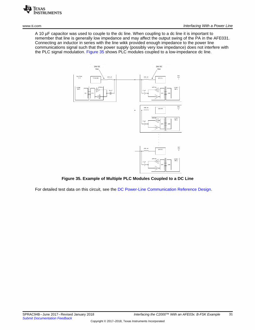
A 10 µF capacitor was used to couple to the dc line. When coupling to a dc line it is important toremember that line is generally low impedance and may affect the output swing of the PA in the AFE031.Connecting an inductor in series with the line wikk provided enough impedance to the power linecommunications signal such that the power supply (possibly very low impedance) does not interfere withthe PLC signal modulation. Figure 35 shows PLC modules coupled to a low-impedance dc line.
Figure 35. Example of Multiple PLC Modules Coupled to a DC Line
For detailed test data on this circuit, see the DC Power-Line Communication Reference Design.
MOV
PAFilterDACSPI SPIPhase
Neutral
AFE031C2000
MOVTVS
PA
Power Supply
D1
D2
D3
Low-Voltage
Capacitor
High-Voltage
Capacitor
N1 N2
+ +
Interfacing With a Power Line www.ti.com
32 SPRAC94B–June 2017–Revised January 2018Submit Documentation Feedback
Copyright © 2017–2018, Texas Instruments Incorporated
Interfacing the C2000™ With an AFE03x: B-FSK Example
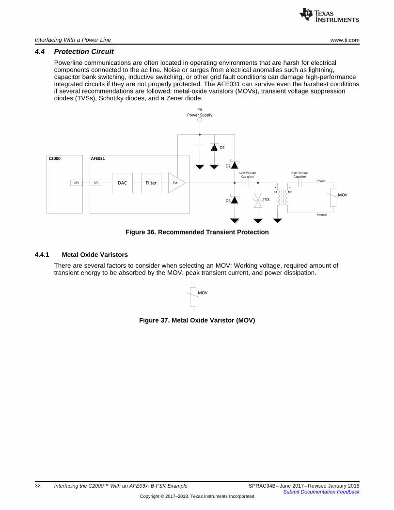
4.4 Protection CircuitPowerline communications are often located in operating environments that are harsh for electricalcomponents connected to the ac line. Noise or surges from electrical anomalies such as lightning,capacitor bank switching, inductive switching, or other grid fault conditions can damage high-performanceintegrated circuits if they are not properly protected. The AFE031 can survive even the harshest conditionsif several recommendations are followed: metal-oxide varistors (MOVs), transient voltage suppressiondiodes (TVSs), Schottky diodes, and a Zener diode.
Figure 36. Recommended Transient Protection
4.4.1 Metal Oxide VaristorsThere are several factors to consider when selecting an MOV: Working voltage, required amount oftransient energy to be absorbed by the MOV, peak transient current, and power dissipation.
Figure 37. Metal Oxide Varistor (MOV)

www.ti.com Interfacing With a Power Line
33SPRAC94B–June 2017–Revised January 2018Submit Documentation Feedback
Copyright © 2017–2018, Texas Instruments Incorporated
Interfacing the C2000™ With an AFE03x: B-FSK Example
A MOV is a device that has high resistance until its triggering voltage is exceeded. Once this voltage levelhas been exceeded, the MOV reduces its resistance and absorbs the energy from the pulse. The I/Vcharacteristic of a typical MOV is shown in Figure 38.
Figure 38. Typical MOV I/V Characteristic

TVS
Interfacing With a Power Line www.ti.com
34 SPRAC94B–June 2017–Revised January 2018Submit Documentation Feedback
Copyright © 2017–2018, Texas Instruments Incorporated
Interfacing the C2000™ With an AFE03x: B-FSK Example
By the nature of the materials and techniques used in the construction of these components, MOVsrespond quickly to a fast transient pulse, have high instantaneous power ratings, and are well-suited forprotection on the ac line. The maximum clamping voltages are typically specified in response to a high-speed transient similar to that shown in Figure 39. The 8/20 µs waveform is commonly associated as awaveform that represents the spectral content of lightning strikes.
Figure 39. Typical 8/20-µs Pulse for MOV and TVS Performance Specification
4.4.2 Transient Voltage SuppressorsA TVS is a very fast-acting clamping device that turns on in the case of an overvoltage condition, shuntingthe surge of current into ground. TVSs are rated primarily by the power handling capability and theclamping voltage. TVSs are available in either unidirectional or bi-directional configurations.
Figure 40. Bi-Directional TVS Diode
www.ti.com Interfacing With a Power Line
35SPRAC94B–June 2017–Revised January 2018Submit Documentation Feedback
Copyright © 2017–2018, Texas Instruments Incorporated
Interfacing the C2000™ With an AFE03x: B-FSK Example
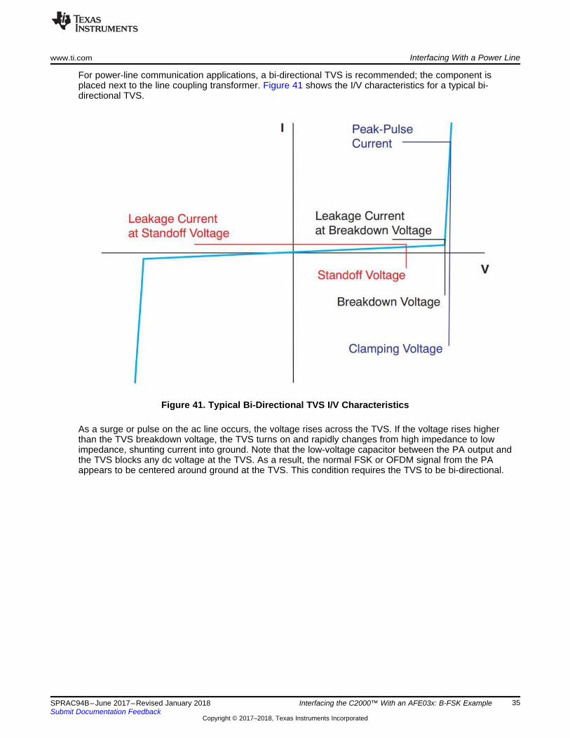
For power-line communication applications, a bi-directional TVS is recommended; the component isplaced next to the line coupling transformer. Figure 41 shows the I/V characteristics for a typical bi-directional TVS.
Figure 41. Typical Bi-Directional TVS I/V Characteristics
As a surge or pulse on the ac line occurs, the voltage rises across the TVS. If the voltage rises higherthan the TVS breakdown voltage, the TVS turns on and rapidly changes from high impedance to lowimpedance, shunting current into ground. Note that the low-voltage capacitor between the PA output andthe TVS blocks any dc voltage at the TVS. As a result, the normal FSK or OFDM signal from the PAappears to be centered around ground at the TVS. This condition requires the TVS to be bi-directional.

Interfacing With a Power Line www.ti.com
36 SPRAC94B–June 2017–Revised January 2018Submit Documentation Feedback
Copyright © 2017–2018, Texas Instruments Incorporated
Interfacing the C2000™ With an AFE03x: B-FSK Example
Figure 42 illustrates this concept.
Figure 42. Typical Signal at the TVS
Because the signal is symmetric around ground at the TVS, the TVS breakdown voltage should be equalto approximately one-half of the PA power-supply voltage. It is important for the TVS to remain off duringnormal operation to avoid clipping and introducing distortions to the output signal. It is also important thatthe TVS turn on and clamp at the lowest possible voltage beyond normal operation to provide maximumprotection.
This BoosterPack was designed with surge protection parts. A bi-directional transient-voltage suppression(TVS) diode with a shunt connection to attach on the LV side of the transformer is used to clamp thevoltage of a surge. The stable voltage of the TVS must be exactly 1/2 of the PA supply voltage of the AFE,meaning a 15-V AFE must use a 7.5-V TVS. This 1/2 ratio is based on the fact that:• The PA of the AFE is a type AB, which uses a single power rail. So, the 12-V powered PA TX output is
at a 6-V bias with a ±6-V amplitude, meaning that the signal has a ±6-V range. While on transmission,the TVS must not be allowed to saturate the signal, so the stable voltage must be kept to ≥ ½ of thePA power rail.
• If a 12-V PA uses a 7.5-V TVS, during the arrival of a surge pulse, the LV side bias is locked-on at 7.5V, but if the surge occurs at the exact moment of a TX maximum amplitude (which is 6 V), then thesignal on the TX route is 7.5 V + 6 V = 13.5 V, which is higher than the power rail and causes damageto the PA of the AFE. So, the TVS voltage must be ≤ 1/2 of the PA power rail.
� �2.878 1.5 2 2 8.25SupplyPA V V V u � u
� �2Supply Load SwingPA V Turns Ratio V u u u
Zener
Diode
Schottky
Diode
www.ti.com Interfacing With a Power Line
37SPRAC94B–June 2017–Revised January 2018Submit Documentation Feedback
Copyright © 2017–2018, Texas Instruments Incorporated
Interfacing the C2000™ With an AFE03x: B-FSK Example
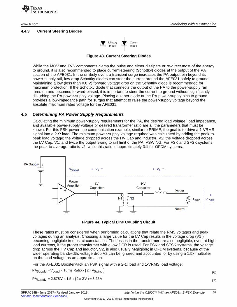
4.4.3 Current Steering Diodes
Figure 43. Current Steering Diodes
While the MOV and TVS components clamp the pulse and either dissipate or re-direct most of the energyto ground, it is also recommended to place current-steering (Schottky) diodes at the output of the PAsection of the AFE031. In the unlikely event a transient surge increases the PA output pin beyond itspower-supply rail, low-drop Schottky diodes can steer the current around the AFE031 safely to ground.Maintaining a low (less than 0.8 V) forward voltage drop on the Schottky diode is recommended formaximum protection. If the Schottky diode that connects the output of the PA to the power-supply railturns on and becomes forward-biased, it is important to steer the current to ground without significantlydisturbing the PA power-supply voltage. Placing a zener diode at the PA power-supply pins to groundprovides a low-impedance path for surges that attempt to raise the power-supply voltage beyond theabsolute maximum rated voltage for the AFE031.
4.5 Determining PA Power Supply RequirementsCalculating the minimum power-supply requirements for the PA, the desired load voltage, load impedance,and available power-supply voltage or desired transformer ratio are all the parameters that must beknown. For this FSK power-line communication example, similar to PRIME, the goal is to drive a 1-VRMSsignal into a 2-Ω load. The minimum power-supply voltage required was calculated by adding the peak-to-peak load voltage; the voltage dropped across the HV Cap and inductor, V2; the voltage dropped acrossthe LV Cap, V1; and twice the output swing to rail limit of the PA, VSWING. For FSK and SFSK systems,the peak-to-average ratio is √2, while this ratio is approximately 3:1 for OFDM systems.
Figure 44. Typical Line Coupling Circuit
These ratios must be considered when performing calculations that relate the RMS voltages and peakvoltages during an analysis. Choosing a large value for the LV Cap results in the voltage drop (V1 )becoming negligible in most circumstances. The losses in the transformer are also negligible, even at highload currents, if the proper transformer with a low DCR is used. For FSK and SFSK systems, the voltagedrop across the HV Cap and inductor, V2, is also usually negligible; in OFDM systems, because of thewider operating bandwidth, voltage drop V2 can be ignored and accounted for by using a 1.5x multiplieron the load voltage as an approximation.
For the AFE031 BoosterPack an FSK signal with a 2-Ω load and 1-VRMS load voltage:
(6)
(7)

� �2Supply Load SwingPA V OFDM Multiplier Turns Ratio V u u u u u
Summary www.ti.com
38 SPRAC94B–June 2017–Revised January 2018Submit Documentation Feedback
Copyright © 2017–2018, Texas Instruments Incorporated
Interfacing the C2000™ With an AFE03x: B-FSK Example
For OFDM, the following equation can be used:
(8)
For more information on Power dissipation of the AFE031, see AFE Design for a Narrowband PLCModem Using the AFE031 .
5 SummaryThe FSK transmitter provides a stepping stone for communications development using an AFE030/1device with a C2000 F28379D. More development could be done to demonstrate the system as a FSKreceiver. By providing this example, the hope is that someone who is interested in PLC communicationscan pick it up and begin learning. By creating hardware that is flexible enough to be used in multiplemodes allows various communications protocols to be implemented on the same hardware. As a finalreminder, all software and hardware can be found in C2000Ware.
6 References• FSK information:
– Spread-Frequency Shift Keying Power Line Modem Software Architecture• SunSpec Protocol:
– SunSpec Home page• AFE031 Information and Designs:
– AFE Design for a Narrowband PLC Modem Using the AFE031– AFE031 Powerline Communications Analog Front-End Data Sheet– DC Power-Line Communcation Reference Design

39SPRAC94B–June 2017–Revised January 2018Submit Documentation Feedback
Copyright © 2017–2018, Texas Instruments Incorporated
Interfacing the C2000™ With an AFE03x: B-FSK Example
Appendix ASPRAC94B–June 2017–Revised January 2018
Schematics
Schematics (PWM Mode) www.ti.com
40 SPRAC94B–June 2017–Revised January 2018Submit Documentation Feedback
Copyright © 2017–2018, Texas Instruments Incorporated
Interfacing the C2000™ With an AFE03x: B-FSK Example
A.1 Schematics (PWM Mode)
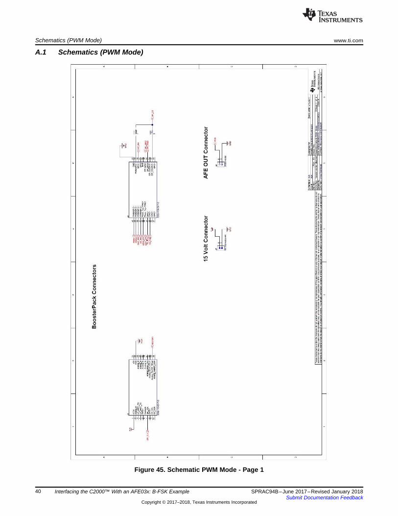
Figure 45. Schematic PWM Mode - Page 1
www.ti.com Schematics (PWM Mode)
41SPRAC94B–June 2017–Revised January 2018Submit Documentation Feedback
Copyright © 2017–2018, Texas Instruments Incorporated
Interfacing the C2000™ With an AFE03x: B-FSK Example
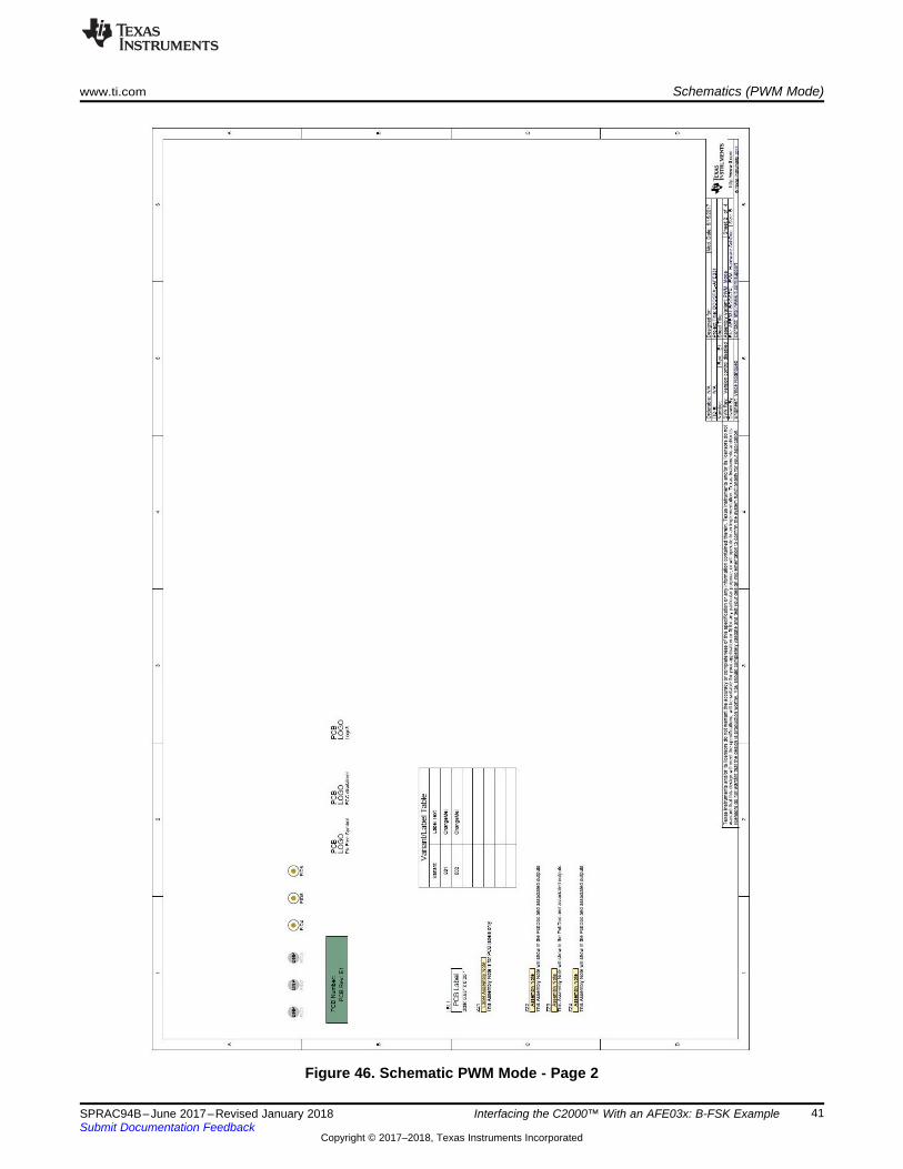
Figure 46. Schematic PWM Mode - Page 2
Schematics (PWM Mode) www.ti.com
42 SPRAC94B–June 2017–Revised January 2018Submit Documentation Feedback
Copyright © 2017–2018, Texas Instruments Incorporated
Interfacing the C2000™ With an AFE03x: B-FSK Example
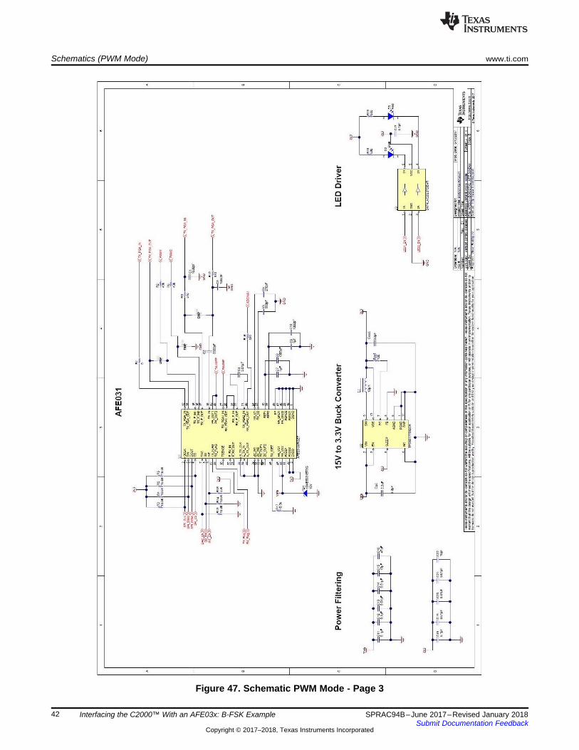
Figure 47. Schematic PWM Mode - Page 3
www.ti.com Schematics (PWM Mode)
43SPRAC94B–June 2017–Revised January 2018Submit Documentation Feedback
Copyright © 2017–2018, Texas Instruments Incorporated
Interfacing the C2000™ With an AFE03x: B-FSK Example
Figure 48. Schematic PWM Mode - Page 4

Schematics (DAC Mode) www.ti.com
44 SPRAC94B–June 2017–Revised January 2018Submit Documentation Feedback
Copyright © 2017–2018, Texas Instruments Incorporated
Interfacing the C2000™ With an AFE03x: B-FSK Example
A.2 Schematics (DAC Mode)
Figure 49. Schematic DAC Mode - Page 1

www.ti.com Schematics (DAC Mode)
45SPRAC94B–June 2017–Revised January 2018Submit Documentation Feedback
Copyright © 2017–2018, Texas Instruments Incorporated
Interfacing the C2000™ With an AFE03x: B-FSK Example
Figure 50. Schematic DAC Mode - Page 2

Schematics (DAC Mode) www.ti.com
46 SPRAC94B–June 2017–Revised January 2018Submit Documentation Feedback
Copyright © 2017–2018, Texas Instruments Incorporated
Interfacing the C2000™ With an AFE03x: B-FSK Example
Figure 51. Schematic DAC Mode - Page 3

www.ti.com Schematics (DAC Mode)
47SPRAC94B–June 2017–Revised January 2018Submit Documentation Feedback
Copyright © 2017–2018, Texas Instruments Incorporated
Interfacing the C2000™ With an AFE03x: B-FSK Example
Figure 52. Schematic DAC Mode - Page 4

Revision History www.ti.com
48 SPRAC94B–June 2017–Revised January 2018Submit Documentation Feedback
Copyright © 2017–2018, Texas Instruments Incorporated
Revision History
Revision HistoryNOTE: Page numbers for previous revisions may differ from page numbers in the current version.
Changes from A Revision (December 2017) to B Revision ........................................................................................... Page
• Updates were made in Section 3.3.3.4. .............................................................................................. 27

IMPORTANT NOTICE FOR TI DESIGN INFORMATION AND RESOURCES
Texas Instruments Incorporated (‘TI”) technical, application or other design advice, services or information, including, but not limited to,reference designs and materials relating to evaluation modules, (collectively, “TI Resources”) are intended to assist designers who aredeveloping applications that incorporate TI products; by downloading, accessing or using any particular TI Resource in any way, you(individually or, if you are acting on behalf of a company, your company) agree to use it solely for this purpose and subject to the terms ofthis Notice.TI’s provision of TI Resources does not expand or otherwise alter TI’s applicable published warranties or warranty disclaimers for TIproducts, and no additional obligations or liabilities arise from TI providing such TI Resources. TI reserves the right to make corrections,enhancements, improvements and other changes to its TI Resources.You understand and agree that you remain responsible for using your independent analysis, evaluation and judgment in designing yourapplications and that you have full and exclusive responsibility to assure the safety of your applications and compliance of your applications(and of all TI products used in or for your applications) with all applicable regulations, laws and other applicable requirements. Yourepresent that, with respect to your applications, you have all the necessary expertise to create and implement safeguards that (1)anticipate dangerous consequences of failures, (2) monitor failures and their consequences, and (3) lessen the likelihood of failures thatmight cause harm and take appropriate actions. You agree that prior to using or distributing any applications that include TI products, youwill thoroughly test such applications and the functionality of such TI products as used in such applications. TI has not conducted anytesting other than that specifically described in the published documentation for a particular TI Resource.You are authorized to use, copy and modify any individual TI Resource only in connection with the development of applications that includethe TI product(s) identified in such TI Resource. NO OTHER LICENSE, EXPRESS OR IMPLIED, BY ESTOPPEL OR OTHERWISE TOANY OTHER TI INTELLECTUAL PROPERTY RIGHT, AND NO LICENSE TO ANY TECHNOLOGY OR INTELLECTUAL PROPERTYRIGHT OF TI OR ANY THIRD PARTY IS GRANTED HEREIN, including but not limited to any patent right, copyright, mask work right, orother intellectual property right relating to any combination, machine, or process in which TI products or services are used. Informationregarding or referencing third-party products or services does not constitute a license to use such products or services, or a warranty orendorsement thereof. Use of TI Resources may require a license from a third party under the patents or other intellectual property of thethird party, or a license from TI under the patents or other intellectual property of TI.TI RESOURCES ARE PROVIDED “AS IS” AND WITH ALL FAULTS. TI DISCLAIMS ALL OTHER WARRANTIES ORREPRESENTATIONS, EXPRESS OR IMPLIED, REGARDING TI RESOURCES OR USE THEREOF, INCLUDING BUT NOT LIMITED TOACCURACY OR COMPLETENESS, TITLE, ANY EPIDEMIC FAILURE WARRANTY AND ANY IMPLIED WARRANTIES OFMERCHANTABILITY, FITNESS FOR A PARTICULAR PURPOSE, AND NON-INFRINGEMENT OF ANY THIRD PARTY INTELLECTUALPROPERTY RIGHTS.TI SHALL NOT BE LIABLE FOR AND SHALL NOT DEFEND OR INDEMNIFY YOU AGAINST ANY CLAIM, INCLUDING BUT NOTLIMITED TO ANY INFRINGEMENT CLAIM THAT RELATES TO OR IS BASED ON ANY COMBINATION OF PRODUCTS EVEN IFDESCRIBED IN TI RESOURCES OR OTHERWISE. IN NO EVENT SHALL TI BE LIABLE FOR ANY ACTUAL, DIRECT, SPECIAL,COLLATERAL, INDIRECT, PUNITIVE, INCIDENTAL, CONSEQUENTIAL OR EXEMPLARY DAMAGES IN CONNECTION WITH ORARISING OUT OF TI RESOURCES OR USE THEREOF, AND REGARDLESS OF WHETHER TI HAS BEEN ADVISED OF THEPOSSIBILITY OF SUCH DAMAGES.You agree to fully indemnify TI and its representatives against any damages, costs, losses, and/or liabilities arising out of your non-compliance with the terms and provisions of this Notice.This Notice applies to TI Resources. Additional terms apply to the use and purchase of certain types of materials, TI products and services.These include; without limitation, TI’s standard terms for semiconductor products http://www.ti.com/sc/docs/stdterms.htm), evaluationmodules, and samples (http://www.ti.com/sc/docs/sampterms.htm).
Mailing Address: Texas Instruments, Post Office Box 655303, Dallas, Texas 75265Copyright © 2018, Texas Instruments Incorporated