inter-plane stitching for optimum high-speed digital ...interplane.pdf · inter-plane stitching for...
TRANSCRIPT

Inter-Plane Stitching for Optimum
High-Speed Digital Signal Integrity
By Robert C. Trautman
©2014
As electronics design engineers we will put on a number of different hats during the
design, development, and testing phases of our circuits and systems. With operating speeds
running well into the gigahertz throughout the past decade, we must be ever more vigilant when
it comes to routing our circuits on Printed Wiring Boards (PWB). Whether you do your own
PWB routing, hand it off to another group within your company, or send it out to be done, it is
more important now than ever before to fully understand the transmission line effects of the
copper traces in our circuits, and how they affect high-speed digital signal integrity.
PWB designers are very capable at their often very tedious and difficult jobs, but some
may not have a deep understanding of transmission line theory. In fact, almost every PWB
designer I’ve ever worked with has been a mechanical engineer. Just as they wouldn’t expect me
to know all of the subtleties of torque conversion or achieving the optimal chamfer (I’d hope), I
wouldn’t expect them to know subtle aspects of transmission line theory. It simply isn’t in their
educational curricula. To the credit of those who route PWBs, no matter what credentials they
carry, they’ve always done quite a good job for me when gently guided, even though they might
not have been formally trained in the more esoteric concepts of electronics theory. It is,
therefore, our responsibility, as the electrical guys (and gals) who have had this training, to
prepare and present as much information as practicable when sending our designs off to be
routed. To do that, we need to understand the effects of transmission lines in circuit boards
thoroughly, ourselves.
With 35-years as a EE under my belt, I’ve watched the not-so-subtle creation of discrete
specialties within our field; Digital circuits, power supplies, analog circuits, RF circuits, and
others. Interestingly, over the past decade, I’ve also started to see these separate design areas
starting to converge again like they’d been prior to the 1970s. In retrospect, this lends validity to
the then-amusing, now-prophetic words of the very seasoned supervisor of the school’s
electronics lab where I’d worked until I graduated at 21. He said, “Digital is just a fad. We live in
an analog world!” That said, I know that there are still a lot of EEs out there who only do digital
design, and might have forgotten the basics of transmission line theory that the RF guys (and
gals) would consider second nature. This represents a disturbing chasm when circuits are now
running more than three orders of magnitude faster than they did in the late 1970s. This article is
designed to help bridge that gap.
When discussing esoteric concepts of electronic theory, I know that pictures speak
volumes. This was my goal in 2005 when I performed a series of experiments with very high
voltage pulses from the first of two versions of a Marx high voltage pulse generator that I’d
constructed at home. Those results were published in Dr. Howard Johnson’s High-Speed Digital
Design Newsletter (Vol. 8, Issue 8), titled “Visible Return Current”. Figure 1 shows the second
version Marx high voltage pulse generator that I built. It was twice as powerful as the first
version, and, like that one, used mostly household items. For the Marx II I used stained oak

boards for the frame, Mylar page protectors and copper foil for the 50kV capacitors, and brass
upholstery tacks for the calibrated ladder-spark-gaps. Throw in some wire, a few scrounged
resistors, an old flyback transformer scavenged from a defunct CRT monitor, a 555 timer circuit,
a high-power FET, and a 24V DC power supply, and I was making sparks in no time!
Figure 1
Irwin Marx had developed his HV pulse generator in 1924 specifically to generate
subatomic particles for nuclear research before the cyclotron, the synchrotron, or even the linear
accelerator yet existed. I built my device for somewhat different reasons. I wanted to subtly
interest my then teenage sons in electronics. I felt that if I could show them something
spectacular…something loud, bright, and dangerous, it’d capture their attention without feeling
like I was pushing my own interests onto them. Well, it half-worked, but that’s another story.
For those who might be inclined to do similarly, I’m compelled to offer a few words of
caution. This is not a toy. Unlike the Van de Graff generator’s fanciful electrostatic sparks, these
sparks have significant current behind them!

Additionally, each ear-splitting discharge also produces an EMP (Electro-Magnetic
Pulse) that is strong enough to damage/disable electronic equipment within about a 10-foot
radius. It produces X-rays, and a wide-band RF signal that would violate FCC regulations if each
momentary discharge lasted much more than just a nanosecond. The Marx generator shown in
Figure 1 produces three nine-inch long (1/4 million Volt) sparks per second. A Faraday cage
keeps the damaging EMI emissions contained.
So, what do these hobbyist atom smashers have to do with transmission line theory as
applied to high-speed digital circuits in printed circuit boards? I can tell you honestly that this
concept wasn’t even on my radar when I built the first generator, so I can truly understand your
skepticism. It was a purely serendipitous observation that took me from the spectacular, nearly
megavolt sparks into bowls of water, to return current paths in circuit boards with high-speed
signals. As Louis Pasteur is quoted as having said, “Chance favors the prepared mind.” I noted
that the tendrils branching off across the surface of the water were not uniform about the spark’s
point of impact as I’d expected. They appeared to be distorted in the shape of the long curved
ground wire inches beneath the water’s surface. I was pretty good with transmission line theory
in school, so I found myself suddenly correlating this bend of the current seeking a path to
ground with that which is associated with high-speed digital return current in a transmission line
structure such as a PWB!
We’ve all been taught that the return current of a high-speed digital signal does not take a
direct, straight-line path through the ground plane back to the source, as will a constant Direct
Current. Instead, it follows the contours of the signal trace. For years I’d accepted this as fact
even though I’d never seen it. In fact, nobody had ever seen it visually…until that fateful day in
2005 when I made a high-speed return current visible in a return-plane-analogue using a quarter
of a million volt pulse
Figure 2 illustrates this concept using a sheet of Plexiglas with conductive squares
forming a grid upon it. This acts as a continuous ground plane, but with spaces between squares
allowing the current to illuminate its own path. A wide strip of copper is affixed to the backside
of the sheet. This forms the signal trace. The long horizontal metal strip on the very bottom is
connected to the generator’s return wire. The purpose of this strip is to eliminate any bias for the
return current. If it didn’t have high-speed qualities to it, then the signal, introduced at the
bottom-right portion of the trace on the back, would show a return path straight down towards
the ground collector strip once it arced over to the front at the top-left. But, because this signal
does have sharp edges, the return current clearly follows the shape of the signal trace on the
opposite side of the Plexiglas.
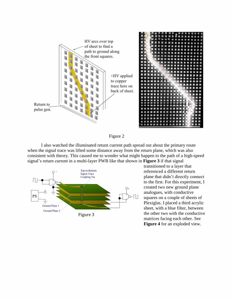
Figure 2
I also watched the illuminated return current path spread out about the primary route
when the signal trace was lifted some distance away from the return plane, which was also
consistent with theory. This caused me to wonder what might happen to the path of a high-speed
signal’s return current in a multi-layer PWB like that shown in Figure 3 if that signal
transitioned to a layer that
referenced a different return
plane that didn’t directly connect
to the first. For this experiment, I
created two new ground plane
analogues, with conductive
squares on a couple of sheets of
Plexiglas. I placed a third acrylic
sheet, with a blue filter, between
the other two with the conductive
matrices facing each other. See
Figure 4 for an exploded view.
Figure 3

Figure 4
For this experiment, I needed to make the front trace, in particular,
transparent so I could view the return current spark behind it. I
accomplished this by using some fine mesh metal screen material
formed in the shape of the traces I wanted. I then connected the
ends of the front and rear traces at the center of the sheets using a
stiff red wire forming a wide radius to avoid an inadvertent arc to
the return planes during the transition of the signal from the front
trace to the back trace, as shown in Figure 5. This red wire is
represented in Figure 4 as the dotted red line, suggesting
effectively a direct connection – a via – from the front to rear
traces. The return wire back to the generator is connected to the
bottom row of the front-most return plane grid.
Figure 5
Figures 4 and 5 are both drawn showing the Plexiglas perimeter just outside of the grids.
This was necessary in order to fit the given image area, but, in reality, this perimeter extended
out no less than six inches on the closest side in order to prevent arcing around the edges. The
actual test setup, showing this wide perimeter, is shown in Figure 6.

Figure 6
With this apparatus and grid configuration, I was able to clearly see visual evidence of
the path that the return current took within each of the two different return planes. The theory
we’re all taught in relation to return current flowing in a return plane directly beneath the signal
trace always implies a single, contiguous trace on one signal layer, referencing one contiguous
ground/return plane. This most definitely is the optimal configuration for high-speed signal
traces, but it’s not always possible to achieve this ideal in a high-density PWB. Let’s see what
happens when a high-speed signal trace transitions layers and picks up a new return plane.
Figure 7 shows a well-behaved return current path. This is because I’ve coupled the front and
back return planes directly at the point of the signal transition (see the green circle near the
center). Because of the blue filter between front and back Plexiglas sheets, the spark following
the rear-most return plane grid is seen as blue, and it won’t precisely align with the front squares,
while that of the front return is naturally white, and traces a path between each of the applicable
visible squares.
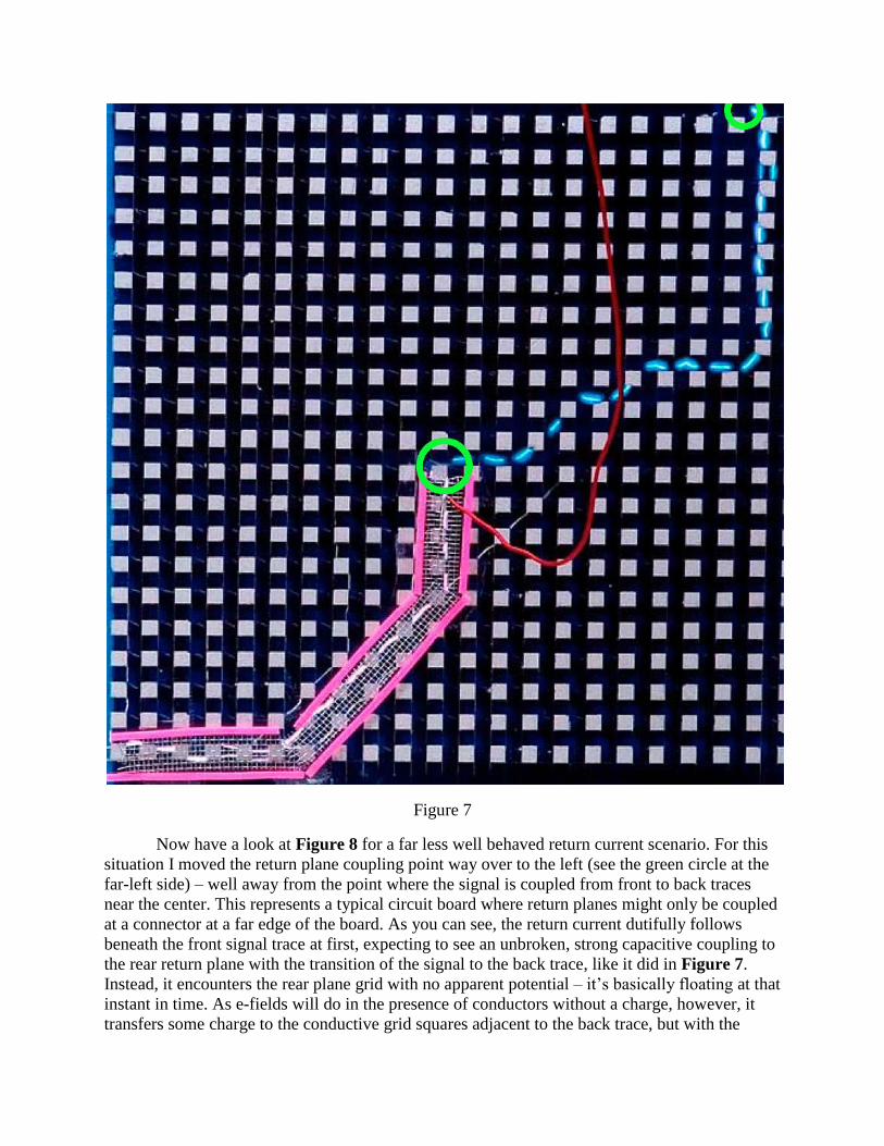
Figure 7
Now have a look at Figure 8 for a far less well behaved return current scenario. For this
situation I moved the return plane coupling point way over to the left (see the green circle at the
far-left side) – well away from the point where the signal is coupled from front to back traces
near the center. This represents a typical circuit board where return planes might only be coupled
at a connector at a far edge of the board. As you can see, the return current dutifully follows
beneath the front signal trace at first, expecting to see an unbroken, strong capacitive coupling to
the rear return plane with the transition of the signal to the back trace, like it did in Figure 7.
Instead, it encounters the rear plane grid with no apparent potential – it’s basically floating at that
instant in time. As e-fields will do in the presence of conductors without a charge, however, it
transfers some charge to the conductive grid squares adjacent to the back trace, but with the

absence of an opposing charge, there is no significant current flow between these squares. At the
same time that the signal wavefront is moving up the back trace to the right, the distant sensation
of a return path far to the left is starting to be “felt” by these charged squares. This causes a
secondary wavefront to travel over to the left side where it’ll finally find a direct path to ground
through the coupling to the front grid. This creates a high-current path that then causes current to
flow between each of the squares of the back grid, finally meeting the end of the signal trace at
the top-right.
Figure 8

Ignoring the long red interconnecting wire – as this is for illustrative purposes only – the
return current path in Figure 7 is equal to that of the signal trace length. Also, all portions of
both the front and back signal traces are properly referenced to their respective (nearest) ground
planes. As such, the signal shape arriving at the destination is very well behaved. Comparing this
to Figure 8, you can clearly see that the return current is now following two separate paths, and
they’re significantly longer than the signal path. Not only will the current profile at both source
and destination be severely distorted, thus distorting the wave shape, but the brief loss of a strong
ground reference will also significantly affect the effective trace impedance. All of these issues
add up to increased reflections and poor wave shapes at the destination. What can be done to
improve waveshapes that have been so distorted? Introduce inter-plane return-current stitches!
While admittedly obscure, the concept of such stitches is nothing new. They’ve been
suggested in a number of publications as early as about 2002, as far as I’m aware. What IS new
is that I’ve just made return current visible. Such visual evidence clearly illustrates just how
severe return current detours can be when we don’t use inter-plane stitches close to signal
transitions in high-speed digital circuits. Few formulas can make as much of an impact on the
engineering community, as a whole, as can brilliant spark photos!
In its most basic form, a return current stitch can be a simple copper via that connects
applicable return planes together local to where high-speed signals transition layers. Figure 9
shows a digital signal launched into an eight-inch copper trace starting on Layer 1. This signal is
referenced to ground on Layer 2. You can see that the return current is immediately established
between these layers, thus creating an impedance of around 50-Ohms. Figure 10 gives us a
snapshot of the signal and its return current about half a nanosecond later where it reaches the
end of the three-inch portion of the signal trace on Layer 1.
The signal transitions from Layer 1 to Layer 10 through a copper via. The return planes
(Layer’s 2 & 9) are coupled with another via (a stitch) right next to that which carries the signal.
Figure 11 gives us another snapshot as the return current propagates along with the signal’s
wavefront in a well-behaved manner, continuing to exhibit an unbroken 50-Ohm impedance.
Finally, in Figure 12, the signal and return current both reach the load simultaneously. As there
is no imbalance in the time between signal and return current, and the impedance has remained
consistent throughout, there will be very little reflection or other distortions, thus providing an
optimal waveshape at the load.

Figure 9
Figure 10

Figure 11
Figure 12

Figures 13 - 17, show precisely the same circuit, except that it does not use an inter-plane
stitch to couple the return planes on Layers 2 & 9. Figures 13 and 14 look very similar to their
Figure 9 equivalents. For the half-nanosecond that the signal travels along the trace on Layer 1,
referenced to return Layer 2, a consistent 50-Ohm impedance will be established. The signal
doesn’t run into problems until it reaches Layer 10. It’s e-field is radiating out, but, at that instant
in time, it can’t “feel” the influence of the return path that had been established back on Layer 2,
so it really doesn’t know where to go. It will, of course, couple into the closest metal, Layer 9,
but it has no direction, therefore, there is no return current, thus, no signal reference. For the
period of time that the signal edge travels along Layer 10 (Figure 15), the trace impedance will
suddenly jump far above its initial 50-Ohms. Figure 16 shows the signal flowing through the
load, finally giving it a path back to the source, but there is no transmission line structure to
establish the impedance yet. Eventually, as shown in Figure 17, the return current will find its
way back to the source, but it’s taken twice the time it should have.
What have we seen here? Just because there was no inter-plane return-current stitch via,
there’s a huge impedance disparity at point of the signal transition, and the return current takes
twice as long to get back to the source. Both of these issues contribute to major reflections and
poor waveshape.
Figure 13

Figure 14
Figure 15

Figure 16
Figure 17

How close does the return-current stitch need to be to the signal via in order to be
effective at maintaining a consistent impedance structure after the signal transitions layers? This
depends upon a couple of factors: 1) How fast is the edge-rate (rise or fall time) of your signal?
2) How fast does your circuit board propagate that signal? Remember, an electronic signal does
not travel along the copper traces of a circuit board at the speed of light. In actuality, such signals
propagate at just half of that speed in a common circuit board. The dielectric constant (r) of the
circuit board material will determine the speed of propagation, and usually the frequency of the
signal will dictate the rise and fall times of its edges in order to produce a well-formed square
wave. Just plug those numbers into Formula 1, and it will give you the recommended maximum
distance that the inter-plane via stitch needs to be from the signal via in order to create an
effective return-current path for the signal.
Formula 1
Where:
d = Distance in inches
c = Speed of light (299,792,458 meters per second)
r = Dielectric constant of circuit board (usually between 3.0 and 4.9)
tr = Rise time (or fall time) of signal edge in nanoseconds
As you can see, the faster the edge rate, the closer the return-current stitch needs to be to
the signal via. This formula is an approximation, but its results are suitable to provide your PWB
people with guidelines for critical signals if layer transitions cannot be avoided. If there is
already a power or ground via going to a decoupling capacitor, that connects the appropriate
planes together, within a reasonable radius of the signal transition via, then no special inter-plane
stitch via is required.
I’m sure that some of you are asking if our 2D and 3D field solvers have been lying to us.
They indicate that we’ll have a nice, consistent impedance when we make the traces with a
certain copper weight a specific width, spaced a particular distance from a return plane, and yet
here it’s obvious that we’ll have a horrendous impedance mismatch if the signal transitions
layers without using an inter-plane stitch. No, they’re not lying to us…exactly. They just didn’t
tell us everything, thus allowing us to make the logical-seeming leap that an impedance structure
on one set of layers will be the same on any other set of layers…without doing anything special
to make this happen. Using inter-plane return-current stitches, these impedance structures will
work as advertised. Otherwise, they will not.
What if, instead of transitioning from Layer 1 to Layer 10, the signal went to Layer 7? Its
closest reference plane is the +3.3V power on Layer 6. Obviously we can’t put a copper via
stitch between Layers 2 (GND) and Layer 6 (+3.3V) without creating what I’d call a good old-
fashioned fuse! Since we don’t like things burning up inside of our circuit boards, the solution in

this situation is to install a small capacitor (10pF to 100pF, depending on target frequency)
between Layers 2 and 6 near the via where the signal transitioned from Layer 1 to 7.
As I’ve effectively illustrated herein, it is very important to provide local paths for return
current back to the source such that proper trace impedance can be maintained throughout.
Without this, severe reflections and the accompanying wave shape distortion will occur. With
reduced margins at increased operating frequencies, such distortion can make an otherwise
clean-seeming design fail. Installing copper or capacitive stitches between planes, as applicable,
where high-speed signals transition is the best way to ensure well-behaved return current paths,
resulting in consistent impedance paths and well-behaved waveforms.
Author’s Bio:
Bob Trautman is an electronics engineer with 35-years of professional experience. Electronics
has been both his hobby and his passion for nearly 48 years. He is also a licensed helicopter
pilot, a professional portrait photographer, and a published author in both magazines and books.
He has two boys (now grown), and lives in Owego, NY.
References:
“High-Speed Signal Propagation: Advanced Black Magic” by Dr. Howard Johnson & Martin
Graham (2003)