intel scalable performance board design...
TRANSCRIPT

Intel® 440BX AGPset / PGA370 Scalable Performance Board Design Guide
October 2001
Order Number: 273296-005

Information in this document is provided in connection with Intel® products. No license, express or implied, by estoppel or otherwise, to any intellectual property rights is granted by this document. Except as provided in Intel’s Terms and Conditions of Sale for such products, Intel assumes no liability whatsoever, and Intel disclaims any express or implied warranty, relating to sale and/or use of Intel products including liability or warranties relating to fitness for a particular purpose, merchantability, or infringement of any patent, copyright or other intellectual property right. Intel products are not intended for use in medical, life saving, or life sustaining applications.
Intel may make changes to specifications and product descriptions at any time, without notice.
Designers must not rely on the absence or characteristics of any features or instructions marked “reserved” or “undefined.” Intel reserves these for future definition and shall have no responsibility whatsoever for conflicts or incompatibilities arising from future changes to them.
The Intel® 440BX AGPset, Intel Celeron™ processor, and Intel Pentium® III processor may contain design defects or errors known as errata which may cause the products to deviate from published specifications. Current characterized errata are available on request.
Contact your local Intel sales office or your distributor to obtain the latest specifications and before placing your product order.
Copies of documents which have an ordering number and are referenced in this document, or other Intel literature may be obtained by calling 1-800-548-4725 or by visiting Intel’s website at http://www.intel.com.
Copyright © Intel Corporation, 2000
*Third-party brands and names are the property of their respective owners.

Intel® 440BX AGPset / PGA370 Scalable Performance Board Design Guide
Contents1.0 Introduction ..................................................................................................................7
1.1 Notation and Terminology .....................................................................................71.2 Reference Documents and Resources .................................................................81.3 Design Features ....................................................................................................9
1.3.1 PGA370-Based Processors .....................................................................91.3.2 Intel® 440BX AGPset ...............................................................................9
1.4 General Considerations.......................................................................................101.4.1 Voltage Definitions .................................................................................101.4.2 General Design Recommendations .......................................................10
1.5 Transitioning from an Intel® Pentium® II Processor / 440BX AGPset Design .................................................................................................................111.5.1 AGTL+ Termination ................................................................................111.5.2 VREF Inputs ............................................................................................111.5.3 System Bus Clock ..................................................................................111.5.4 CMOS Compatibility with Future Processors .........................................111.5.5 Processor Core Voltage Decoupling ......................................................121.5.6 VID[4] Pin ...............................................................................................121.5.7 Phase Lock Loop (PLL) Power...............................................................12
1.5.7.1 PLL Topology ............................................................................121.5.7.2 PLL Filter Specification..............................................................131.5.7.3 PLL Filter Recommendation......................................................14
1.5.8 Bus Frequency Selection .......................................................................151.5.9 New Pin Definitions ................................................................................151.5.10 VCOREDET ..............................................................................................15
2.0 Layout and Routing Guidelines..........................................................................16
2.1 BGA Quadrant Assignment .................................................................................162.2 PGA370-Based Processor Signal Quadrants .....................................................172.3 Board Description................................................................................................202.4 Routing Guidelines ..............................................................................................21
2.4.1 AGTL+ Description .................................................................................212.5 AGTL+ Layout Recommendations ......................................................................21
2.5.1 Network Topology and Conditions .........................................................212.5.2 Recommended Trace Lengths ...............................................................22
2.5.2.1 Board Layout Rules...................................................................222.5.3 Additional Guidelines..............................................................................23
2.6 Pre-Layout Simulation (Sensitivity Analysis) .......................................................232.6.1 Simulation Parameter Values.................................................................232.6.2 Simulation Methodology .........................................................................23
2.6.2.1 Flight Time Simulation...............................................................242.6.2.2 Signal Quality Measurement .....................................................25
2.7 Post-Layout Simulation .......................................................................................252.7.1 Crosstalk and the Multi-Bit Adjustment Factor .......................................25
2.8 Timing Analysis ...................................................................................................262.9 Host Clock Routing Spacing................................................................................27
2.9.1 System Clock Layout..............................................................................282.10 Other Buses ........................................................................................................29
3

Intel® 440BX AGPset / PGA370 Scalable Performance Board Design Guide
3.0 Scalable Performance Board Guidelines ....................................................... 30
3.1 Processor Guidelines .......................................................................................... 303.1.1 Scalable Performance System Design DC Guidelines........................... 303.1.2 System Bus AC Guidelines .................................................................... 323.1.3 Thermal Guidelines ................................................................................ 35
3.2 PGA370 Socket Design Guidelines .................................................................... 363.2.1 VTT and VCCCORE Power Plane Split ..................................................... 363.2.2 BSEL[1:0] Implementation ..................................................................... 363.2.3 CLKREF Circuit Implementation ............................................................373.2.4 AGTL+ Reset Implementation................................................................ 38
3.2.4.1 AGTL+ Reset Layout Topology................................................. 393.2.5 CMOS Voltage Conversion Logic........................................................... 40
4.0 Design Checklist ...................................................................................................... 41
4.1 Overview ............................................................................................................. 414.2 Pull-up and Pull-down Resistor Values ............................................................... 414.3 Processor Checklist ............................................................................................42
4.3.1 PGA370-Based Processors ................................................................... 424.3.2 GND and Power Pin Definition............................................................... 454.3.3 Processor Clocks ................................................................................... 454.3.4 Processor Signals .................................................................................. 464.3.5 Processor Decoupling Capacitors.......................................................... 47
4.3.5.1 Core Voltage High-Frequency Decoupling................................ 474.3.5.2 VTT Decoupling.........................................................................474.3.5.3 VREF Decoupling...................................................................... 48
4.4 Board Component Keep-Out...............................................................................484.5 Thermals/Cooling Solutions ................................................................................ 49
4.5.1 Thermal Solution Design Considerations...............................................494.6 Mechanical Design Considerations..................................................................... 494.7 Electrical Design Considerations ........................................................................ 50
5.0 Third-Party Vendor Information .........................................................................51
5.1 Voltage Regulator Control Silicon ....................................................................... 515.2 Clock Drivers....................................................................................................... 515.3 PGA370 Socket...................................................................................................51
Index .............................................................................................................................. 53
4

Intel® 440BX AGPset / PGA370 Scalable Performance Board Design Guide
Figures
1 PLL Filter Topology .............................................................................................122 PLL Filter Specification........................................................................................133 Using Discrete R .................................................................................................154 No Discrete R ......................................................................................................155 Major Signal Sections of the 82443BX (Top View) .............................................166 PGA370-Based Processor Quadrants ................................................................177 Example ATX Placement for Intel® 440BX AGPset / PGA370-Based
Processor Designs ..............................................................................................188 Example NLX Placement for Intel® 440BX AGPset / PGA370-Based
Processor Design ................................................................................................199 Four-Layer Board Stack-up Example ..................................................................2010 Recommended Topology ....................................................................................2111 Test Load vs. Actual System Load......................................................................2412 Clock Trace Spacing Guidelines .........................................................................2713 Host Clock Topology ...........................................................................................2914 BCLK Waveform..................................................................................................3315 Processor System Bus Valid Delay Timings Waveform......................................3416 Processor System Bus Setup and Hold Timings.................................................3417 Power-On Reset and Configuration Timings.......................................................3518 BSEL[1:0] Circuit Implementation for PGA370 Designs......................................3619 CLKREF Circuit Implementation for PGA370 Designs........................................3720 AGTL+ Reset Implementation.............................................................................3821 AGTL+ Reset Layout Topology...........................................................................3922 CMOS Conversion Logic.....................................................................................4023 Pull-up Resistor Example ....................................................................................4224 Example Capacitor Placement Within the PGA370 Socket ................................4725 Board Component Keep-Out...............................................................................48
5
Intel® 440BX AGPset / PGA370 Scalable Performance Board Design Guide
6
Tables
1 Reference Documents and Resources ................................................................. 82 Recommended Inductor for PLL Filter ................................................................ 143 Recommended Capacitor for PLL Filter.............................................................. 144 Recommended Resistor for PLL Filter ................................................................ 145 Recommended Trace Lengths............................................................................ 226 Parameter Values for Interconnect AGTL+ Simulations ..................................... 237 PGA370-Based Processor and Intel® 440BX AGPset System
Timing Equations ................................................................................................ 268 PGA370-Based Processor and Intel® 440BX AGPset System
Timing Terms ...................................................................................................... 269 Recommended 66/100 MHz System Bus Timing Parameters............................2710 Host Clock Trace Lengths................................................................................... 2811 Voltage and Current Specifications1, 2 for PGA370-Based Processors .............. 3012 Scalable Performance Board Processor System Bus AC Guidelines (Clock)1,2,3
at the Processor Pins .......................................................................................... 3213 Processor System Bus AC Guidelines (AGTL+ Signal Group)1, 2, 3, 4
at the Processor Pins .......................................................................................... 3314 Intel® Celeron™ Processor PPGA Thermal Design Power ................................ 3515 Intel® Pentium® III Processor for the PGA370 Socket Thermal
Design Power...................................................................................................... 3516 Resistor Values for CLKREF Divider (3.3 V Source) .......................................... 3717 AGTL+ Connectivity ............................................................................................4218 CMOS Connectivity............................................................................................. 4319 TAP Connectivity (optional)................................................................................. 4420 Clock Connectivity............................................................................................... 4421 Miscellaneous Connectivity................................................................................. 4422 Power Connectivity ............................................................................................. 4523 No Connects ....................................................................................................... 45
Revision History
Revision Date Description
005 10/01 Updated note on page 36.
004 5/00 Removed VTT and VCCCORE Voltage Sequencing section (3.2.2 in the -003 version).
003 5/00 Renamed document to remove references to “motherboard” and “flexible platform.” The corrected term is now “scalable performance board.” Clarified “CMOS Compatibility with Future Processors” on page 11. Clarified “BSEL[1:0] Implementation” on page 36. Updated Figure 25 with new component keep-out restrictions. Corrected power dissipation specification to 26.7 W. Added VTT and VCCCORE Power Plane Split section and VTT and VCCCORE Voltage Sequencing sec-tion.
002 2/00 Clarified core voltage high frequency decoupling recommendations. Updated Figure 20 and Figure 21.
001 11/99 First publication of this document.

Intel® 440BX AGPset / PGA370 Scalable Performance Board Design Guide
For ble ates
A
1.0 Introduction
The Intel® Celeron™ and Intel Pentium® III processor families include processors that can be installed in a PGA370 socket. This document provides design recommendations and considerations for developing systems based on the Celeron processor in a PPGA package or the Pentium III processor in an FC-PGA package, together with the Intel 440BX AGPset. Likely design considerations are included to alleviate problems during the design and debug phases.
The information contained in this document should be used in conjunction with the Intel® 440BX AGPset Design Guide, which covers Intel 440BX AGPset designs with the Intel Pentium II processor. Refer to that document for topics not covered in this design guide. Exceptions to the Intel® 440BX AGPset Design Guide are listed in this document.
1.1 Notation and Terminology
In this document, a ‘#’ symbol after a signal name identifies the signal as active low; that is, a signal that is in the active state, based on the name of the signal, when driven to a low level.example, when FLUSH# is low, a flush has been requested. When NMI is high, a nonmaskainterrupt has occurred. When a signal name does not imply an active state, a # symbol indicthat the signal is inverted. For example, D[3:0] = ‘HLHL’ refers to a hex ‘A’, and D[3:0]# = ‘LHLH’ also refers to a hex ‘A’ (H= High logic level, L= Low logic level).
The term “PGA370-based processor(s)” refers to the Celeron processor in a PPGA or FC-PGpackage and the PentiumIII processor in an FC-PGA package.
7

Intel® 440BX AGPset / PGA370 Scalable Performance Board Design Guide
1.2 Reference Documents and Resources
Table 1. Reference Documents and Resources
Document Name or Information Source Order Number
Pentium® III Processor for the PGA370 Socket at 500E MHz and 550E MHz datasheet 245264
Intel® Pentium® III Processor Specification Update 244453
Intel® Pentium® III Processor Thermal Metrology for CPUID 068xh Family Processors 245301
Intel® Celeron™ Processor datasheet 243658
Intel® Celeron™ Processor Specification Update 243748
Intel® 440BX AGPset: 82443BX Host Bridge/Controller datasheet 290633
82443BX Host Bridge/Controller Electrical and Thermal Timing Specification - Datasheet Addendum 273218
Intel® 440BX AGPset Design Guide 290634
Intel® 440BX AGPset Design Guide Update 290641
82443BX Application Notes Contact your Intel Field Sales Representative
Intel® 440BX AGPset: 82443BX Host Bridge/Controller Specification Update 290639
Pentium® II Processor Developer’s Manual 243502
Pentium® II Processor Thermal Design Guidelines 243331
82371AB PCI-TO-ISA/IDE Xcelerator (PIIX4) datasheet 290562
82371AB PCI-TO-ISA/IDE Xcelerator (PIIX4) Timing Specifications - Datasheet Addendum 290548
Intel® 82371EB (PIIX4E) Specification Update 290635
370-pin Socket (PGA370) Design Guidelines 244410
PGA370 Heat Sink Cooling in MicroATX Chassis 245025
CK97 CLock Synthesizer Design Guidelines 243867
P6 Family of Processors Hardware Developer’s Manual 244001
8

Intel® 440BX AGPset / PGA370 Scalable Performance Board Design Guide
D) d essor. Grant,
r is A) ow ssors level-
ate
1.3 Design Features
1.3.1 PGA370-Based Processors
The PGA370-based processors implement a dynamic execution microarchitecture and execute Intel MMX™ technology instructions for enhanced media and communication performance. Additionally, the PentiumIII processors feature streaming single instruction, multiple data (SIMextensions for enhanced floating-point and 3-D application performance. The PGA370-baseprocessors also use the same multi-transaction system bus used in the Intel Pentium II procThe PGA370-based processors support multiple low-power states such as AutoHALT, Stop-Sleep, and Deep Sleep to conserve power during idle times.
The PGA370-based processors are based on the P6 processor core. The Celeron processoprovided in a Plastic Pin Grid Array (PPGA) package and a Flip-Chip Pin Grid Array (FC-PGpackage, and the PentiumIII processor is optionally provided in a FC-PGA package for use in lcost systems in the value embedded computing market segment. The PGA370-based proceutilize the AGTL+ system bus used by the Pentium II processor with support limited to singleprocessor-based systems. The Celeron processor (PPGA) includes an integrated 128-Kbytetwo cache with a separate 16-Kbyte instruction and 16-Kbyte data level-one caches. The PentiumIII processor (FC-PGA) includes an integrated 256-Kbyte level-two cache with separ16-Kbyte instruction and 16-Kbyte data level-one caches. The level-two cache is capable of caching 64 Gbyte of system memory address space.
1.3.2 Intel® 440BX AGPset
The Intel 440BX AGPset is a two-component chipset that includes the 82443BX AGP Host Bridge Controller and the 82371AB PCI-TO-ISA/IDE Xcelerator (PIIX4).
The chipset has the following features:
• Support for single Celeron or Pentium III processor configuration
• 64-bit AGTL+ based host bus interface
• 32-bit AGTL+ based host address interface
• 64-bit main memory interface with optimized support for SDRAM at 100 MHz and 66 MHz
• 32-bit primary PCI bus interface (PCI) with an integrated PCI arbiter
• AGP interface (AGP) with 133 MHz data transfer capability configurable as a secondary PCI bus
• Extensive data buffering between all interfaces for high throughput and concurrent operations
• Mobile and “Deep Green” desktop power management support
9

Intel® 440BX AGPset / PGA370 Scalable Performance Board Design Guide
1.4 General Considerations
1.4.1 Voltage Definitions
For the purposes of this document, the following nominal voltage definitions are used:
Note: VCC1.5 and VTT must be sourced by the same voltage regulator.
1.4.2 General Design Recommendations
• Intel recommends using a widely available, programmable Voltage Regulator Module (VRM) installed in a VRM header or an on-board programmable voltage regulator. Please see the VRM 8.4 DC-DC Converter Design Guidelines.
• Board designs targeted for system integrators should be designed according to the boxed processor electrical, mechanical, and thermal specifications provided in the boxed processor section of the Intel® Celeron™ Processor datasheet and the Pentium® III Processor for the PGA370 Socket datasheet. The most notable items are the required fan power header and fan/heatsink physical clearance on the board.
VCC 5.0 V
VCC3.3 3.3 V
VCCCORE Voltage is dependent on the four bit VID setting
VCC2.5 2.5 V
VCC1.5 1.5 V
VCCCMOS 1.5 V or 2.5 V depending on processor
VTT 1.5 V
VREF 1.0 V
AGPVREF 1.32 V
10

Intel® 440BX AGPset / PGA370 Scalable Performance Board Design Guide
e es
mils
set and tails
w the
d ds
1.5 Transitioning from an Intel® Pentium® II Processor / 440BX AGPset Design
The following sections detail the considerations for transitioning from a Intel 440BX AGPset / SC-242 connector design to a PGA370 socket design.
1.5.1 AGTL+ Termination
Intel recommends 56 Ω ± 5% resistors for AGTL+ termination on the board. In addition, high frequency VTT decoupling is also required on the system board. Intel recommends 19 or mor0.1µF capacitors in the 0603 package with one capacitor for every two resistor packs (assumfour resistors per pack).
1.5.2 VREF Inputs
VREF (2/3 VTT) must be supplied to the processor through each of the eight VREF inputs. Intel recommends using one 75Ω ± 1% and 150Ω ± 1% resistor divider of the VTT supply to generate VREF. Intel also recommends placing four 0.1 µF capacitors in the 0603 package within 500of the processor’s VREF pins.
1.5.3 System Bus Clock
Due to the change in system bus trace lengths in the FC-PGA and PPGA packages, the chipprocessor clocks must be tied together to minimize pin-to-pin clock skew. Implementation deare provided in Section 2.5, “AGTL+ Layout Recommendations” on page 21.
It is also recommended that a capacitor site be placed near the processor BCLK input to alloclock skew to be minimized through tuning. This can be done by changing the value at the capacitor site to compensate for the actual board trace lengths.
1.5.4 CMOS Compatibility with Future Processors
All PGA370-based processor CMOS outputs are open drain and require a pull-up to drive toexternal logic. The 0.18 micron process technology utilizes 1.5 V-compatible CMOS signals anthe 0.25 micron process technology utilizes 2.5 V-compatible CMOS signals. Intel recommenthe following CMOS design guidelines.
Intel has defined three new pins for the all PGA370-based processors:
• VCC2.5: This pin should be connected to the system’s 2.5 V supply.
• VCC1.5: This pin should be connected to the system’s 1.5 V supply.
• VCCCMOS: This pin should be used as the system CMOS pull-up voltage. A 0.1 µF decoupling capacitor is recommended.
VCC1.5 and VTT are recommended to be sourced by the same voltage regulator.
The VCCCMOS pin provides the CMOS voltage for the pull-up resistors required on the system board. A 2.5 V source must be provided to the VCC2.5 pin and a 1.5 V source must be provided to the VCC1.5 pin. The source for VCC1.5 must be the same as the one supplying VTT. The processor routes the compatible CMOS voltage source (1.5 V or 2.5 V) through the package and out to the
11

Intel® 440BX AGPset / PGA370 Scalable Performance Board Design Guide
erall .1,
e quiet
l ch alues.
VCCCMOS output pin. Processors based on 0.25 micron process technology (such as the Intel Celeron processor) use 2.5 V CMOS buffers. Processors based on 0.18 micron process technology (such as the Pentium III processor for the PGA370 socket) use 1.5 V CMOS buffers.
These pins have been defined to permit a maximum current of 500 mA.
1.5.5 Processor Core Voltage Decoupling
The system board must implement high frequency decoupling for the processor core voltage. Intel recommends that ten or more 4.7 µF capacitors in the 1206 package (ceramic X5R or better material) be placed within the socket cavity. Placement of the capacitors should minimize ovinductance between VCC/VSS power pins. Implementation details are provided in Section 4.3.5“Core Voltage High-Frequency Decoupling” on page 47.
1.5.6 VID[4] Pin
The Voltage ID pin VID[4] is not available on the processor. Therefore, according to the VRM 8.4 DC-DC Converter Guidelines, VID[4] must be connected to ground on the voltage regulator in order to provide the correct VID[3:0] for 1.30 V to 2.05 V voltage ID encoding.
1.5.7 Phase Lock Loop (PLL) Power
All PGA370-based processors have internal PLL clock generators that are analog and requirpower supplies to minimize jitter.
1.5.7.1 PLL Topology
The general desired topology is shown in Figure 1. Not shown are parasitic routing and locadecoupling capacitors. Excluded from the external circuitry are parasitics associated with eacomponent. See Section 1.5.7.3, “PLL Filter Recommendation” on page 14 for R, L, and C v
Figure 1. PLL Filter Topology
v004
R L
C
PLL2
PLL1
PLL
VSS = 0V
370-PinSocket
VCCCORE
12

Intel® 440BX AGPset / PGA370 Scalable Performance Board Design Guide
1.5.7.2 PLL Filter Specification
The function of the filter is to protect the PLL from external noise through low-pass attenuation. In general, the low-pass description forms an adequate description for the filter.
The low-pass specification, with input at VCCCORE and output measured across the capacitor, is as follows:
< 0.2 dB gain in pass band
< 0.5 dB attenuation in pass band (see DC drop in the notes that follow Figure 2)
> 34 dB attenuation from 1 MHz to 66 MHz
> 28 dB attenuation from 66 MHz to core frequency
The filter specification is graphically shown in Figure 2.
NOTES:1. Diagram not to scale.2. No specification for frequencies beyond fcore.3. fpeak, if it exists, should be less than 0.05 MHz.
Other requirements of the PLL filter are:
• The filter should support DC current > 30 mA.
• A shielded type inductor is required to minimize magnetic pickup.
• The DC voltage drop from VCC to PLL1 should be < 60 mV, which in practice implies series R < 2 Ω; this also means that pass band attenuation (from DC to 1 Hz) is < 0.5 dB for VCC = 1.1 V, and < 0.35 dB for VCC = 1.5 V.
Figure 2. PLL Filter Specification
0dB
-28dB
-34dB
0.2dB
x dB
1 MHz 66 MHz fcorefpeak1HzDC
passbandhigh frequency
bandx = 20.log[(Vcc-60mV)/Vcc]
filt 1 d
13

Intel® 440BX AGPset / PGA370 Scalable Performance Board Design Guide
t,
ce 2.0 -
1.5.7.3 PLL Filter Recommendation
The following tables are examples of components that meet Intel’s recommendations, when configured in the topology shown in Figure 1.
To satisfy damping requirements, total series resistance in the filter (from VCCCORE to the top plate of the capacitor) must be at least 0.35Ω. This resistor can be in the form of a discrete componenor routing, or both. For example, if the selected inductor has a minimum DCR of 0.25Ω, then a routing resistance of at least 0.10Ω is required. Be careful not to exceed the maximum resistanrule (2Ω). For example, if using discrete R1, the maximum DCR of the L should be less than1.1 = 0.9Ω, which precludes using some inductors.
Other routing requirements:
• C should be close to PLL1 and PLL2 pins, < 0.1 Ω per route. These routes do not count towards the minimum damping R requirement.
• The PLL2 route should be parallel and next to PLL1 route (to minimize loop area).
• L should be close to C; any routing resistance should be inserted between VCCCORE and L.
• Any discrete R should be inserted between VCCCORE and L.
Table 2. Recommended Inductor for PLL Filter
Part Number Value Tolerance SRF Rated I DCR
TDK MLF2012A4R7KT 4.7 µH 10% 35 MHz 30 mA 0.56 Ω
Murata LQG21N4R7K00T1 4.7 µH 10% 47 MHz 30 mA 0.70 Ω
Murata LQG21C4R7N00 4.7 µH 30% 35 MHz 30 mA 0.30 Ω
Table 3. Recommended Capacitor for PLL Filter
Part Number Value Tolerance ESL ESR
Kemet T495D336M016AS 33 µF 20% 2.5 nH 0.225 Ω
AVX TPSD336M020S0200 33 µF 20% TBD 0.200 Ω
Table 4. Recommended Resistor for PLL Filter
Value Tolerance Power Note
1 Ω 10% 1/16 W Resistor may be implemented with trace resistance, in which discrete R is not needed.
14

Intel® 440BX AGPset / PGA370 Scalable Performance Board Design Guide
etails
ard
1.5.8 Bus Frequency Selection
The PGA370-based processors utilize the BSEL[0] pins to select 66 MHz and 100 MHz from the CK100 clock synthesizer. Implementation details are provided in Section 3.0, “Scalable Performance Board Guidelines” on page 30.
1.5.9 New Pin Definitions
The following new pins are required for correct operation of the processor. Implementation dare provided in Section 3.0, “Scalable Performance Board Guidelines” on page 30.
1.5.10 VCOREDET
The VCOREDET pin is not used in the Intel 440BX AGPset / PGA370 scalable performance bodesign.
Figure 3. Using Discrete R
Figure 4. No Discrete R
v005
L
C
<0.1 ohm route
PLL2
PLL1
370-PinSocket
<0.1 ohm route
R
VCCCORE
Discrete Resistor
v006
L
C
<0.1 ohm route
PLL2
PLL1
370-PinSocket
<0.1 ohm route
VCCCORE
Trace Resistance
CLKREF Requires a 1.25 V source
EDGCTRL Requires a 51 Ω ± 5% pull-up to VCCCORE
RESET2# Additional reset pin to the processor
RTTCTRL Requires a 110 Ω ± 1% pull-down to VSS
SLEWCTRL Requires a 110 Ω ± 1% pull-down to VSS
15

Intel® 440BX AGPset / PGA370 Scalable Performance Board Design Guide
2.0 Layout and Routing Guidelines
This section describes layout and routing recommendations for ensuring a robust design. Follow these guidelines as closely as possible. Any deviations from the guidelines listed here should be simulated to ensure that adequate margin is maintained in the design.
2.1 BGA Quadrant Assignment
Intel assigned pins on the 82443BX to simplify routing and keep board fab costs down by permitting a board to be routed in four layers. Figure 5 shows the four signal quadrants of the 82443BX. The component placement on the board should be done with this general flow in mind. This simplifies routing and minimizes the number of signals that must cross. The individual signals within the respective groups have also been optimized in order to be routed using only two PCB layers.
For a complete list of signals and ball assignments, see the Intel® 440BX AGPset: 82443BX Host Bridge/Controller datasheet.
Figure 5. Major Signal Sections of the 82443BX (Top View)
Pin #1Corner
ABCDEFGHJKLMNPRTUVWYAAABACADAEAF
AGPQuadrant
PCIQuadrant AGTL+
Quadrant
DRAMQuadrant
12
34
56
78
910
1112
1314
1516
1718
1920
2122
2324
2526
16

Intel® 440BX AGPset / PGA370 Scalable Performance Board Design Guide
2.2 PGA370-Based Processor Signal Quadrants
Figure 6 indicates the signal quadrants for all PGA370-based processors. These quadrants are defined to facilitate layout and placement and illustrate the proposed component placement for a PGA370-based processor for both ATX and NLX form factor designs.
I
Figure 6. PGA370-Based Processor Quadrants
Pin Side View
ANAMALAKAJAHAGAFAEADACABAA
ZYXWVUTSRQPNMLKJHGFEDCBA
ANAMALAKAJAHAGAFAEADACABAAZYXWVUTSRQPNMLKJHGFEDCBA
12
34
56
78
910
1112
1314
1516
1718
1920
2122
2324
2526
2728
2930
3132
3334
3536
37
12
34
56
78
910
1112
1314
1516
1718
1920
2122
2324
2526
2728
2930
3132
3334
3536
37
AGTL+ Signals
CMOS
VCCCMOSPLL1, PLL2
Interrupts
17

Intel® 440BX AGPset / PGA370 Scalable Performance Board Design Guide
ATX Form Factor:
• The ATX placement and layout shown in Figure 7 is recommended for a PGA370-based processor / Intel 440BX AGPset system design.
• The example placement shown in Figure 7 shows 4 PCI slots, 2 ISA slots, 3 DIMM sockets, and one AGP connector.
• For an ATX form factor design, the AGP-compliant graphics device can reside either on the board (device down option) or on an AGP connector (up option).
• The trace length limitation between critical connections is addressed in Section 2.5.2, “Recommended Trace Lengths” on page 22.
• Figure 7 is for reference only. The trade-off between the number of PCI and ISA slots, number of DIMM sockets, and other board peripherals must be evaluated for each design.
Figure 7. Example ATX Placement for Intel® 440BX AGPset / PGA370-Based Processor Designs
A7175-01
82443BXC
KB
FAGP Interface
SDRAM Interface
IDE 0/1
SDRAM DIMMs
Pin A1Host Interface
PCI Interface
PC10370-pin Socket
I/O Ports
AGP/PCI1
PIIX4E
A1 Plug
CK
100
18

Intel® 440BX AGPset / PGA370 Scalable Performance Board Design Guide
NLX Form Factor:
• The NLX placement and layout shown in Figure 8 is recommended for a PGA370-based processor / Intel 440BX AGPset system design.
• The example placement below shows 3 DIMM sockets and an AGP compliant device down on the board. For an NLX form factor design, the AGP compliant graphics device may readily be integrated on the board (device down option). The trace length limitation between critical connections is addressed in Section 2.5.2, “Recommended Trace Lengths” on page 22.
• Figure 8 is for reference only; the trade-off between the number of DIMM sockets and other board peripherals must be evaluated for each design.
Figure 8. Example NLX Placement for Intel® 440BX AGPset / PGA370-Based Processor Design
A7176-01
82443BXCKBF
AGP Interface
SDRAM Interface
SDRAM DIMMs
Host Interface
PCI Interface
I/O P
orts
370-pin Socket
CK
100
PC10/ISA Riser
AGP
PIIX4
19
Intel® 440BX AGPset / PGA370 Scalable Performance Board Design Guide
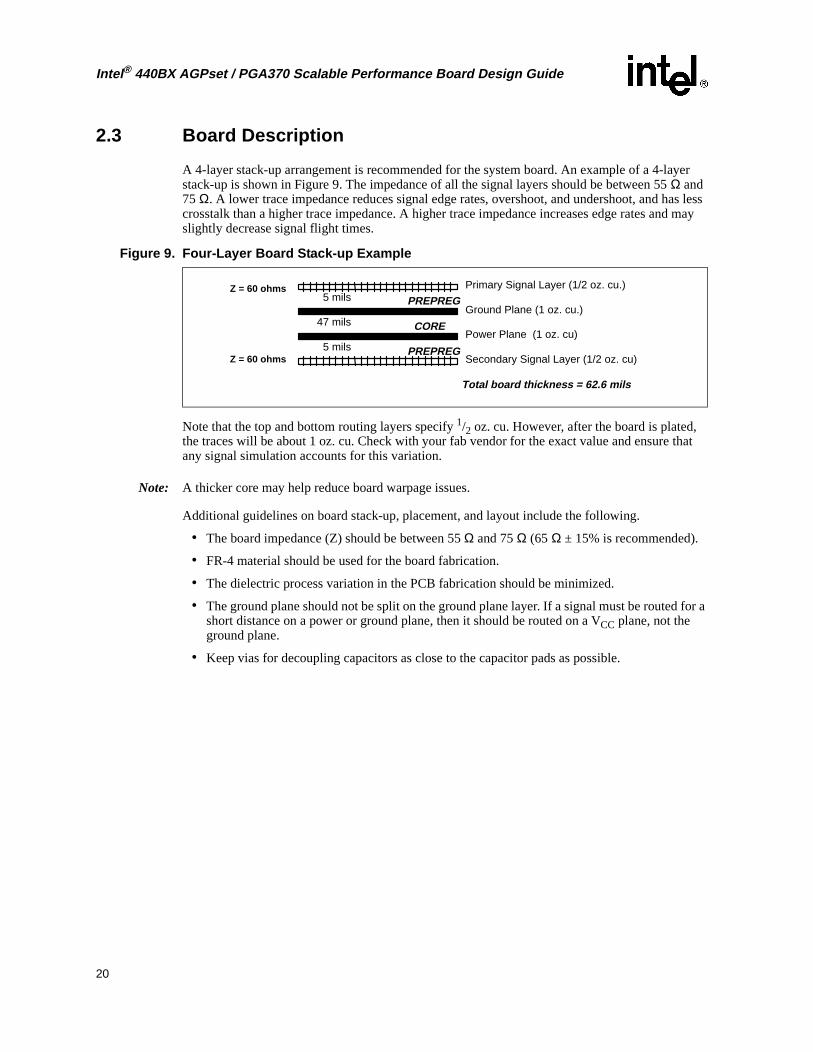
2.3 Board Description
A 4-layer stack-up arrangement is recommended for the system board. An example of a 4-layer stack-up is shown in Figure 9. The impedance of all the signal layers should be between 55 Ω and 75 Ω. A lower trace impedance reduces signal edge rates, overshoot, and undershoot, and has less crosstalk than a higher trace impedance. A higher trace impedance increases edge rates and may slightly decrease signal flight times.
Note that the top and bottom routing layers specify 1/2 oz. cu. However, after the board is plated, the traces will be about 1 oz. cu. Check with your fab vendor for the exact value and ensure that any signal simulation accounts for this variation.
Note: A thicker core may help reduce board warpage issues.
Additional guidelines on board stack-up, placement, and layout include the following.
• The board impedance (Z) should be between 55 Ω and 75 Ω (65 Ω ± 15% is recommended).
• FR-4 material should be used for the board fabrication.
• The dielectric process variation in the PCB fabrication should be minimized.
• The ground plane should not be split on the ground plane layer. If a signal must be routed for a short distance on a power or ground plane, then it should be routed on a VCC plane, not the ground plane.
• Keep vias for decoupling capacitors as close to the capacitor pads as possible.
Figure 9. Four-Layer Board Stack-up Example
Primary Signal Layer (1/2 oz. cu.)
Ground Plane (1 oz. cu.)
Power Plane (1 oz. cu)
Secondary Signal Layer (1/2 oz. cu)
5 mils
47 mils
5 mils
PREPREG
CORE
PREPREG
Z = 60 ohms
Z = 60 ohms
Total board thickness = 62.6 mils
20

Intel® 440BX AGPset / PGA370 Scalable Performance Board Design Guide
2.4 Routing Guidelines
This section lists guidelines to be followed when routing the signal traces during board design. The order in which signals are routed first and last will vary in different designs. Some designers prefer routing all of the clock signals first, while others prefer routing all of the high-speed bus signals first. Either order can be used, as long as the guidelines listed here are followed. If the guidelines listed here are not followed, it is important that your design is simulated, especially on the AGTL+ signals. Even when the guidelines are followed, it is recommended that you simulate as many signals as possible for proper signal integrity, flight time, and crosstalk.
2.4.1 AGTL+ Description
AGTL+ is the electrical bus technology used in the P6 family processors host bus architecture. AGTL+ is a low-output swing, incident wave switching, open-drain bus with external pull-up resistors that provide both the high logic level and termination at the end of the bus. The AGTL+ specification is contained in the Intel® P6 Family Processor Developer’s Manual.
2.5 AGTL+ Layout Recommendations
This section contains the layout recommendations for the AGTL+ signals. The layout recommendations are derived from pre-layout simulations that Intel has performed.
2.5.1 Network Topology and Conditions
Figure 10 shows the recommended topology for 66/100 MHz single processor systems. A termination resistor is placed on the system board. The recommended value for the termination resistor (RTT) is 56 Ω ± 5%.
Figure 10. Recommended Topology
VTT
RTT
L2
L1
Intel® 440BXAGPset
PGA370
21

Intel® 440BX AGPset / PGA370 Scalable Performance Board Design Guide
2.5.2 Recommended Trace Lengths
Table 5 summarizes trace length recommendations. The recommended lengths are derived from the parametric sweeps and Monte Carlo analysis.
The recommended topology for the AGTL+ bus is a single-ended termination topology. A resistor near the processor acts as the pull-up for the bus. In this case, it is recommended that the board trace length be L1.
The actual AGTL+ bus trace width is a standard 5 mil, with minimum edge-to-edge trace spacing set at 12 mils. This helps minimize possible crosstalk effects. The VTT voltage must be held to 1.5 V + 9% (transient condition). It is required that VTT be held to 1.5 V + 3% while the processor system bus is idle (static condition). This is measured at the PGA370 socket pins on the bottom side of the baseboard.
Intel recommends running analog simulations using the available I/O buffer models together with layout information extracted from your specific design. Simulation will confirm that the design adheres to the guidelines.
2.5.2.1 Board Layout Rules
AGTL+ Signals
• AGTL+ signals should be routed with lengths between L1 of trace from the processor pin to the chipset.
• The AGTL+ signals trace length between the processor pin and the resistor pack should be within L2.
• Traces are to be routed with a minimum of 12 mil edge-to-edge spacing, and the ratio of this spacing to the dielectric thickness of the layer should be at least 2:1.
• The trace width is recommended to be 5 mils and not greater than 6 mils.
• The minimum spacing can be decreased to 5 mils for escaping the FC-PGA/PPGA and the BGA areas, for a length of less than 0.25".
• Intel recommends breaking out all signals from the CPU connector on the same layer. If routing is tight, break out from the connector on the opposite routing layer over a ground reference and cross over to the main signal layer near the CPU connector.
• It is strongly recommended that AGTL+ signals be routed on the signal layer next to the ground layer (referenced to ground).
• It is strongly recommended that splits be avoided in the reference plane. Splits disrupt signal return paths and increase overshoot/undershoot due to significantly increased inductance.
• Eliminate parallel traces between layers not separated by a power or ground plane.
• It is strongly recommended that AGTL+ signals do not traverse multiple signal layers.
Note: Following the above layout rules is critical for AGTL+ signal integrity, particularly for processors based on the 0.18 micron process technology.
Table 5. Recommended Trace Lengths
Trace Minimum Length Maximum Length
L1 1.8” 4.3”
L2 0.5” 2.0”
22

Intel® 440BX AGPset / PGA370 Scalable Performance Board Design Guide
eets based on
pins late
ers
2.5.3 Additional Guidelines
General rules for minimizing the impact of crosstalk and other practical considerations in the design of a high speed AGTL+ bus, are provided in the Intel® 440BX AGPset Design Guide.
2.6 Pre-Layout Simulation (Sensitivity Analysis)
2.6.1 Simulation Parameter Values
Parametric Sweeps
The interconnect parameter values that were used in all parametric sweeps are summarized in Table 6.
Note: For simulation purposes, the socket connector can be modeled as a transmission line. The length of the line and the propagation speed must be selected such that they give a total delay of 120 ps in the slow case and 30 ps in the fast case.
2.6.2 Simulation Methodology
Analog simulations are recommended for high-speed system bus designs. Start simulations prior to layout. Pre-layout simulations provide a detailed picture of the working “solution space” that mflight time and signal quality requirements. The layout recommendations in Section 2.5.2 are on pre-layout simulations conducted at Intel. By basing board layout guidelines on the solutispace, the iterations between layout and post-layout simulations can be reduced.
Intel recommends running simulations at the device pads for signal quality and at the devicefor timing analysis. However, simulation results at the device pins may be used later to corresimulation performance against actual system measurements.
Pre-layout analysis includes timing analysis in Section 2.8 and sensitivity analysis using parametric sweeps. Parametric sweep analysis involves varying one or two system parametwhile all others, such as driver strength, package, Zo, and So, are held constant. This way, the
Table 6. Parameter Values for Interconnect AGTL+ Simulations
Parameter Symbol Min Typical Max Tolerance
FC-PGA On-die Termination RTT [Ω] 90 110 130 18%
Board Impedance Z0 [Ω] 74.75 65.00 55.25 15%
Board Velocity S0 [ns/ft] 1.6 2.0 2.2 10-20%
Board TerminationRTT [Ω] 53 56 59 5%
VTT [V] 1.455 1.5 1.545 3%
GTL Reference Voltage VREF[V] 0.95 1.0 1.05 2%
Connector Impedance Z0 [Ω] 50 65 75 N/A
Connector Velocity S0 [ns/ft] 30 100 120 N/A
23

Intel® 440BX AGPset / PGA370 Scalable Performance Board Design Guide
r cessor e and ilable
within
ignal s all nough
s
Bus
sensitivity of the proposed bus topology to varying parameters can be analyzed systematically. The sensitivity of the bus to minimum flight time, maximum flight time, and signal quality should be analyzed as follows:
• Minimum flight time is typically analyzed using fast I/O buffers, a fast package, a fast PGA370 socket, and fast interconnects.
• Maximum flight time is typically analyzed using slow I/O buffers, a slow package, a slow PGA370 socket, and slow interconnects.
• Signal quality is typically analyzed using fast I/O buffers, a slow package, a slow PGA370 socket, and fast interconnects.
The recommended sweep parameter values shown in Table 6 should be used for simulation. The values in Table 6 may be replaced if your supplier’s specific capabilities are known. The cornevalues should comprehend the full range of manufacturing variation. The PGA370-based promodels include the I/O buffer models, core package and socket connector parasitics, packagsocket connector trace length, impedance, and velocity. Intel 440BX AGPset models are avaand include the I/O buffers and package traces. Termination resistors should be controlled to± 5%.
Outputs from each sweep should be analyzed to determine which regions meet timing and squality specifications. To establish the working solution space, find the common space acrosthe sweeps that result in passing timing and signal quality. The solution space should allow edesign flexibility for a feasible, cost-effective layout.
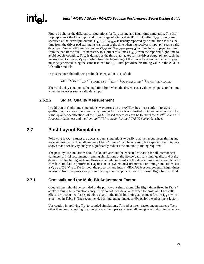
2.6.2.1 Flight Time Simulation
Flight time is the time difference between a signal crossing VREF at the input pin of the receiver and the output pin of the driver crossing VREF where it drives a test load. The timings in the tableand topology discussed in this guideline assume the actual system load is 25Ω for PPGA and 50Ω for FC-PGA and is equal to the test load. The test load can be found in the Processor SystemAC Specifications (GTL+ Signal Group) section of Intel® Celeron™ Processor datasheet and the Pentium® III Processor for the PGA370 Socket datasheet.
Figure 11. Test Load vs. Actual System Load
Q
QSET
CLR
D
RTESTVCC
VTT
TestLoad
I/O Buffer
Q
QSET
CLR
D
RTTVCC
VTT
ActualSystemLoad
I/O Buffer
CLK
CLK
TFLIGHT - SYSTEM
TCO
DriverPin
ReceiverPin
DriverPad
DriverPad
TREF
24
Intel® 440BX AGPset / PGA370 Scalable Performance Board Design Guide
valid
the
time
. The
l has
ct at the ter to
ns, use es
ethod.
le 7
ctor.
ts ctances.
Figure 11 shows the different configurations for TCO testing and flight time simulation. The flip-flop represents the logic input and driver stage of a typical AGTL+ I/O buffer. TCO timings are specified at the driver pin output. TFLIGHT-SYSTEM is usually reported by a simulation tool as the time from the driver pad starting its transition to the time when the receiver’s input pin sees adata input. Since both timing numbers (TCO and TFLIGHT-SYSTEM) will include propagation time from the pad to the pin, it is necessary to subtract this time (TREF) from the reported flight time to avoid double counting. TREF is defined as the time that it takes for the driver output pin to reachmeasurement voltage, VREF, starting from the beginning of the driver transition at the pad. TREF must be generated using the same test load for TCO. Intel provides this timing value in the AGTL+I/O buffer models.
In this manner, the following valid delay equation is satisfied:
Valid Delay = TCO + TFLIGHT-SYS - TREF = TCO-MEASURED + TFLIGHT-MEASURED
The valid delay equation is the total time from when the driver sees a valid clock pulse to thewhen the receiver sees a valid data input.
2.6.2.2 Signal Quality Measurement
In addition to flight time simulations, waveforms on the AGTL+ bus must conform to signal quality specifications to ensure that system performance is not limited by interconnect noisesignal quality specifications of the PGA370-based processors can be found in the Intel® Celeron™ Processor datasheet and the Pentium® III Processor for the PGA370 Socket datasheet.
2.7 Post-Layout Simulation
Following layout, extract the traces and run simulations to verify that the layout meets timing and noise requirements. A small amount of trace “tuning” may be required, but experience at Inteshown that a sensitivity analysis significantly reduces the amount of tuning required.
The post layout simulations should take into account the expected variation for all interconneparameters. Intel recommends running simulations at the device pads for signal quality and device pins for timing analysis. However, simulation results at the device pins may be used lacorrelate simulation performance against actual system measurements. For timing simulatioa VREF of 2/3 VTT ± 2% for both the processor and Intel 440BX AGPset components. Flight timmeasured from the processor pins to other system components use the normal flight time m
2.7.1 Crosstalk and the Multi-Bit Adjustment Factor
Coupled lines should be included in the post-layout simulations. The flight times listed in Tabapply to single bit simulations only. They do not include an allowance for crosstalk. Crosstalkeffects are accounted for separately, as part of the multi-bit timing adjustment factor (Tadj), which is defined in Table 8. The recommended timing budget includes 400 ps for the adjustment fa
Use caution in applying Tadj to coupled simulations. This adjustment factor encompasses effecother than board coupling, such as processor and package crosstalk and ground return indu
25

Intel® 440BX AGPset / PGA370 Scalable Performance Board Design Guide
cation
2.8 Timing Analysis
To determine the available flight time window, perform an initial timing analysis. Analysis of setup and hold conditions will determine the minimum and maximum flight time bounds for the system bus. Use the following equations to establish the system flight time limits.
The terms used in the equations are described in Table 8.
Component timings for the PGA370-based processors are available in the Intel® Celeron™ Processor datasheet and the Pentium® III Processor for the PGA370 Socket datasheet, respectively.
Recommended values for system timings are contained in Table 9. Skew and jitter values for the clock generator device come from the clock driver vendor’s datasheet. The PCB skew specifiis based on the results of extensive simulations at Intel. The Tadj value is based on Intel’s experience with systems that use the Pentium Pro and Pentium II processors.
Table 7. PGA370-Based Processor and Intel® 440BX AGPset System Timing Equations
Driver Receiver Equation
CPU 440BXTflight, min > Thold - Tco,min + Tskew, CLK (CPU leads BX)
Tflight, max < Tcycle - Tco,max - Tsu - Tskew, CLK (BX leads CPU) - Tjit - Tadj
440BX CPUTflight, min > Thold - Tco,min + Tskew, CLK (BX leads CPU)
Tflight, max < Tcycle - Tco,max - Tsu - Tskew, CLK (CPU leads BX) - Tjit - Tadj
Table 8. PGA370-Based Processor and Intel® 440BX AGPset System Timing Terms
Term Description
Tcycle System cycle time, defined as the reciprocal of the frequency.
Tflight,min Minimum system flight time.
Tflight,max Maximum system flight time.
Tco,max Maximum driver delay from input clock to output data.
Tco,min Minimum driver delay from input clock to output data.
TsuMinimum setup time. Defined as the time for which the input data must be valid prior to the input clock.
ThMinimum hold time. Defined as the time for which the input data must remain valid after the input clock.
Tskew,CLK
Clock generator skew. Defined as the maximum delay variation between output clock signals from the system clock generator, the maximum delay variation between clock signals due to system board variation and Intel 440BX AGPset loading variation, and skew due to delay in the PGA370 socket.
Tjit Clock jitter. Defined as the maximum edge to edge variation in a given clock signal.
Tadj
Multi-bit timing adjustment factor. This term accounts for the additional delay that occurs in the network when multiple data bits switch in the same cycle. The adjustment factor includes such mechanisms as package and PCB crosstalk, high inductance current return paths, and simultaneous switching noise.
26

Intel® 440BX AGPset / PGA370 Scalable Performance Board Design Guide
een
The flight time requirements that result from using the component timing specifications and recommended system timings are summarized in Table 7. All component values should be verified against the latest specifications before proceeding with analysis.
2.9 Host Clock Routing Spacing
The PGA370-based processor / Intel 440BX AGPset scalable performance board requires a clock synthesizer for supplying 66/100 MHz system bus clocks, PCI clocks, APIC clocks, SDRAM clocks, and 14 MHz clocks.
To minimize the impact of crosstalk, a minimum of 0.025” spacing should be maintained betwthe clock traces and other traces. A minimum spacing of 0.025” is also recommended for serpentines.
Table 9. Recommended 66/100 MHz System Bus Timing Parameters
Timing Term Value
PGA370-based processors PPGAFC-PGA
Tskew,CLK (CPU leads BX) [ns] 0.6000.250
Tskew,CLK (BX leads CPU) [ns] -0.2500.100
Tjit [ns] 0.25
Tadj [ns] 0.40
Figure 12. Clock Trace Spacing Guidelines
Clo
ck
0.025”
0.025”
27
Intel® 440BX AGPset / PGA370 Scalable Performance Board Design Guide
grity by
gth 0 and
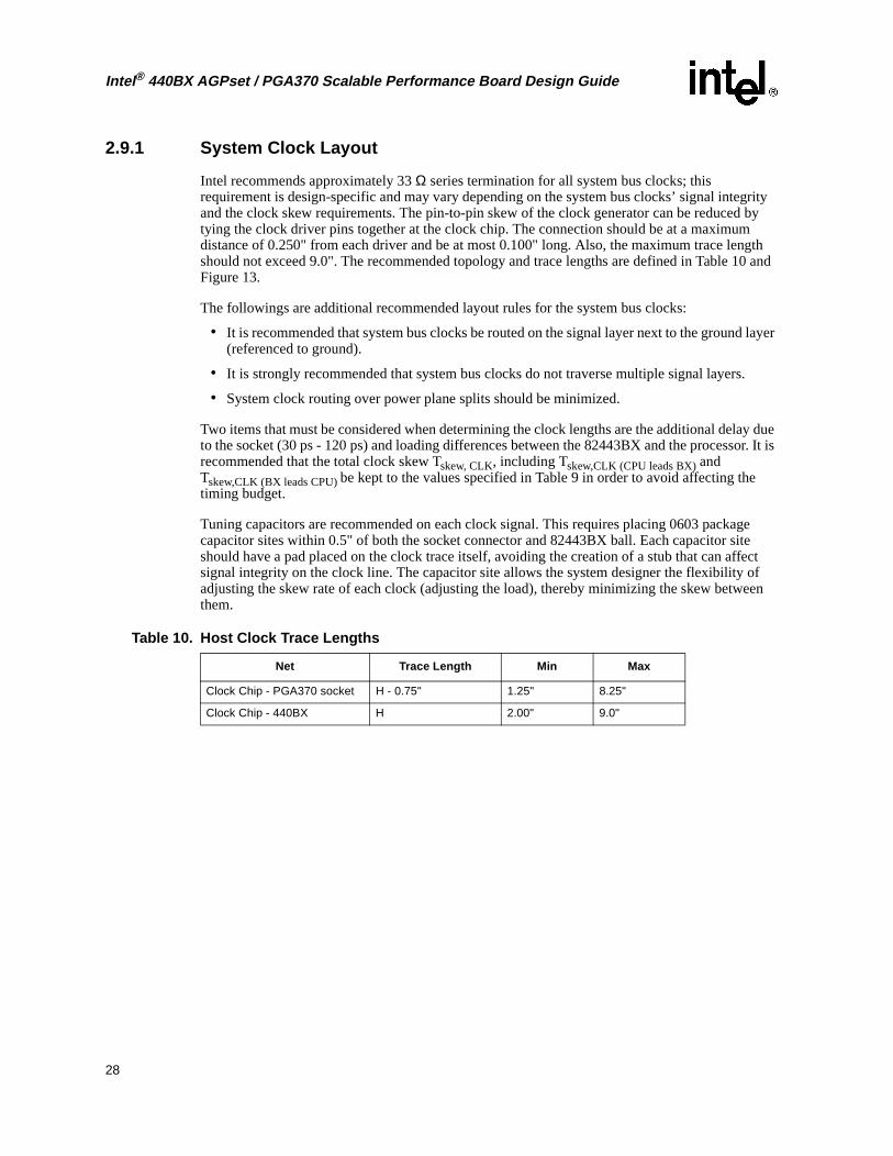
2.9.1 System Clock Layout
Intel recommends approximately 33 Ω series termination for all system bus clocks; this requirement is design-specific and may vary depending on the system bus clocks’ signal inteand the clock skew requirements. The pin-to-pin skew of the clock generator can be reducedtying the clock driver pins together at the clock chip. The connection should be at a maximumdistance of 0.250" from each driver and be at most 0.100" long. Also, the maximum trace lenshould not exceed 9.0". The recommended topology and trace lengths are defined in Table 1Figure 13.
The followings are additional recommended layout rules for the system bus clocks:
• It is recommended that system bus clocks be routed on the signal layer next to the ground layer (referenced to ground).
• It is strongly recommended that system bus clocks do not traverse multiple signal layers.
• System clock routing over power plane splits should be minimized.
Two items that must be considered when determining the clock lengths are the additional delay due to the socket (30 ps - 120 ps) and loading differences between the 82443BX and the processor. It is recommended that the total clock skew Tskew, CLK, including Tskew,CLK (CPU leads BX) and Tskew,CLK (BX leads CPU) be kept to the values specified in Table 9 in order to avoid affecting the timing budget.
Tuning capacitors are recommended on each clock signal. This requires placing 0603 package capacitor sites within 0.5" of both the socket connector and 82443BX ball. Each capacitor site should have a pad placed on the clock trace itself, avoiding the creation of a stub that can affect signal integrity on the clock line. The capacitor site allows the system designer the flexibility of adjusting the skew rate of each clock (adjusting the load), thereby minimizing the skew between them.
Table 10. Host Clock Trace Lengths
Net Trace Length Min Max
Clock Chip - PGA370 socket H - 0.75" 1.25" 8.25"
Clock Chip - 440BX H 2.00" 9.0"
28

Intel® 440BX AGPset / PGA370 Scalable Performance Board Design Guide
2.10 Other Buses
Buses not mentioned in the previous sections should adhere to the recommendations set forth in the Intel® 440BX AGPset Design Guide.
Figure 13. Host Clock Topology
D1
D2
0.250"
0.250" ~33Ω
~33Ω82443BX
PGA370-basedprocessors
tuningcapacitor
tuningcapacitor 0.5"
370-Pin SocketConnector
H
H - 0.75"
0.1"Clock
0.5"
29

Intel® 440BX AGPset / PGA370 Scalable Performance Board Design Guide
3.0 Scalable Performance Board Guidelines
3.1 Processor Guidelines
3.1.1 Scalable Performance System Design DC Guidelines
The processor DC guidelines for scalable system designs provided in this section are defined at the processor pins. Table 11 lists the guidelines for PGA370-based processors. Specifications are valid only if specifications for case temperature, clock frequency, and input voltages are met. Be sure to read all notes associated with each parameter.
Table 11. Voltage and Current Specifications1, 2 for PGA370-Based Processors (Sheet 1 of 2)
Symbol Parameter Core Freq Min Typ Max Unit Notes
VCCCOREVCC for processor core 1.65 V 3, 4, 17
VTT, VCC1.5 Static AGTL+ bus termination voltage 1.455 1.50 1.545 V 1.5 ±3% 5, 16
VTT, VCC1.5 Transient AGTL+ bus termination voltage 1.365 1.50 1.635 V 1.5 ±9% 5
VREFAGTL+ input reference voltage -2% 2/3 VTT +2% V ±2%, 7
VCLKREFCLKREF input reference voltage 1.169 1.25 1.331 V ±6.5%, 15
Baseboard VCCCORE Tolerance, Static
Processor core voltage static tolerance level at the PGA370 socket pins
–0.080 0.040 V 6
Baseboard VCCCORE Tolerance, Transient
Processor core voltage transient tolerance level at the PGA370 socket pins
–0.130 0.080 V 6
ICCCORE ICC for processor core 16.2 A 3, 8, 9
ICCCMOS ICC for VCCCMOS 250 mA
ICLKREFCLKREF voltage supply current 60 µA
IVTTTermination voltage supply current 2.7 A 10
ISGntICC Stop-Grant for processor core 2.5 A 8, 11
ISLPICC Sleep for processor core 2.5 A 8
30

Intel® 440BX AGPset / PGA370 Scalable Performance Board Design Guide
IDSLPICC Deep Sleep for processor core 2.2 A
dICCCORE/dt Power supply current slew rate 240 A/µs 12, 13, 14
dIVTT/dt Termination current slew rate 8 A/µs 12, 13
NOTES:1. Unless otherwise noted, all specifications in this table apply to all processor frequencies.2. All specifications in this table apply only to the PGA370-based processors.3. VCCCORE and ICCCORE supply the processor core and the on-die L2 cache.4. Use the “typical voltage” specification with the “tolerance specifications” to provide correct voltage regulation
to the processor.5. VTT and VCC1.5 must be held to 1.5 V ± 9% while the AGTL+ bus is active. It is required that VTT and VCC1.5
be held to 1.5 V ± 3% while the processor system bus is static (idle condition). The required design target is ±3%; transient noise will add ±9%. This is measured at the PGA370 socket pins on the bottom side of the baseboard.
6. These are the tolerance requirements, across a 20 MHz frequency bandwidth, measured at the processor socket pin on the soldered-side of the board. VCCCORE must return to within the static voltage specification within 100 ms after a transient event; see the VRM 8.4 DC-DC Converter Design Guidelines for further details.
7. VREF should be generated from VTT by a voltage divider of 1% resistors or 1% matched resistors. Refer to the Intel® Pentium® II Processor Developer’s Manual for more details on VREF.
8. Max ICC measurements are measured at VCC typical voltage, under maximum signal loading conditions.9. Voltage regulators may be designed with a minimum equivalent internal resistance to ensure that the output
voltage, at maximum current output, is no greater than the nominal (i.e., typical) voltage level of VCCCORE (VCCCORE_TYP). In this case, the maximum current level for the regulator, ICCCORE_REG, can be reduced from the specified maximum current ICCCORE _MAX and is calculated by the equation:
ICCCORE_REG = ICCCORE_MAX × (VCCCORE_TYP - VCCCORE_STATIC_TOLERANCE) / VCCCORE_TYP
10.The current specified is the current required for a single processor. A similar amount of current is drawn through the termination resistors on the opposite end of the AGTL+ bus, unless single-ended termination is used.
11.The current specified is also for AutoHALT state.12.Maximum values are specified by design/characterization at nominal VCCCORE.13.These values are based on simulation and are averaged over the duration of any change in current. Use
these values to compute the maximum inductance tolerable and the reaction time of the voltage regulator. This parameter is not tested.
14.dICC/dt specifications are measured and specified at the PGA370 socket pins.15.CLKREF must be held to 1.25 V ± 6.5%. This tolerance accounts for a ±5% power supply and ±1% resistor
divider tolerance. It is recommended that the board generate the CLKREF reference from either the 2.5 V or 3.3 V supply. VTT should not be used due to risk of AGTL+ switching noise coupling to this analog reference.
16.Static voltage regulation includes: DC output initial voltage set point adjust, output ripple and noise, and output load ranges specified in the tables above.
17.Listed value is for the Pentium III processor at 850 MHz. Refer to the datasheet for other processor VCCCORE values.
Table 11. Voltage and Current Specifications1, 2 for PGA370-Based Processors (Sheet 2 of 2)
Symbol Parameter Core Freq Min Typ Max Unit Notes
31

Intel® 440BX AGPset / PGA370 Scalable Performance Board Design Guide
3.1.2 System Bus AC Guidelines
Table 12 and Table 13 contain 100 MHz system bus AC guidelines defined at the processor pins.
Table 12 contains the BCLK guidelines and Table 13 contains the AGTL+ system bus guidelines. Processor system bus AC specifications for the AGTL+ signal group at the processor pins for 100 MHz are equivalent to those at 66 MHz. The 66 MHz specification is documented in the processor datasheet.
Table 12. Scalable Performance Board Processor System Bus AC Guidelines (Clock)1,2,3 at the Processor Pins
T# Parameter Min Nom Max Unit Figure Notes
System Bus Frequency 100 MHz All processor core frequencies
T1: BCLK Period 10.0 ns 14 4, 5
T2: BCLK Period Stability ±250 ps 14 5, 6, 7
T3: BCLK High Time 2.5 ns 14 @>2.0 V 5
T4: BCLK Low Time 2.4 ns 14 @<0.5 V
T5: BCLK Rise Time 0.4 1.6 ns 14 (0.5 V–2.0 V) 5
T6: BCLK Fall Time 0.4 1.6 ns 14 (2.0 V–0.5 V) 5
NOTES:1. Unless otherwise noted, all specifications in this table apply to all processor frequencies and cache sizes. 2. All AC timings for the AGTL+ signals are referenced to the BCLK rising edge at 1.25 V at the processor
core pin. All AGTL+ signal timings (address bus, data bus, etc.) are referenced at 1.00 V at the processor core pins.
3. All AC timings for the CMOS signals are referenced to the BCLK rising edge at 1.25 V at the processor core pin. All CMOS signal timings (compatibility signals, etc.) are referenced at 1.25 V at the processor core pins.
4. The BCLK period allows a +0.5 ns tolerance for clock driver variation.5. This specification applies to the processor when operating with a system bus frequency of 100 MHz. 6. Due to the difficulty of accurately measuring clock jitter in a system, it is recommended that a clock driver
be used that is designed to meet the period stability specification into a test load of 10 to 20 pF. This should be measured on the rising edges of adjacent BCLKs crossing 1.25 V at the processor core pin. The jitter present must be accounted for as a component of BCLK timing skew between devices.
7. The clock driver’s closed loop jitter bandwidth must be set low to allow any PLL-based device to track the jitter created by the clock driver. The –20 dB attenuation point, as measured into a 10 to 20 pF load, should be less than 500 KHz. This specification may be ensured by design characterization and/or measured with a spectrum analyzer.
32

Intel® 440BX AGPset / PGA370 Scalable Performance Board Design Guide
Figure 14. BCLK Waveform
Table 13. Processor System Bus AC Guidelines (AGTL+ Signal Group)1, 2, 3, 4 at the Processor Pins
T# Parameter Min Max Unit Figure Notes
System Bus Frequency 100 MHz All processor core frequencies
T7: AGTL+ Output Valid Delay 0.20 3.25 ns 14 5
T8: AGTL+ Input Setup Time 1.20 ns 15 5, 6, 7, 8
T9: AGTL+ Input Hold Time 1.00 ns 15 9
T10: RESET# Pulse Width 1.00 ns 16 7, 10
NOTES:1. Unless otherwise noted, all specifications in this table apply to all processor frequencies.2. These specifications are tested during manufacturing.3. All AC timings for the AGTL+ signals are referenced to the BCLK rising edge at 1.25 V at the processor pin.
All AGTL+ signal timings (compatibility signals, etc.) are referenced at 1.00 V at the processor pins.4. This specification applies to the processor operating with a 66 MHz or 100 MHz system bus.5. Valid delay timings for these signals are specified into 25 Ω to 1.5 V and with VREF at 1.0 V for 66 MHz, and
into 50 Ω to 1.5 V and with VREF at 1.0 V.6. A minimum of three clocks must be guaranteed between two active-to-inactive transitions of TRDY#.7. RESET# can be asserted (active) asynchronously, but must be deasserted synchronously.8. Specification is for a minimum 0.40 V swing.9. Specification is for a maximum 1.0 V swing.
10.After VCCCORE and BCLK become stable.
761a
2.0V1.25V
0.5V
tr
tp
tf
th
tl
CLK
Tr = T5 (Rise Time)Tf = T6 (Fall Time)Th = T3 (High Time)Tl = T4 (Low Time)Tp = T1 (BLCK Period)
33

Intel® 440BX AGPset / PGA370 Scalable Performance Board Design Guide
Figure 15. Processor System Bus Valid Delay Timings Waveform
Figure 16. Processor System Bus Setup and Hold Timings
CLK
Signal
Tx Tx
Tpw
V Valid Valid
Tx T7, T11, T29 (Valid Delay)=
Tpw T14, T15 (Pulse Wdith)=
V 1.0V for GTL+ signal group; 1.25V for CMOS, APIC and JTAG signal groups=
CLK
Signal V Valid
Ts T8, T12, T27 (Setup Time)=
Th T9, T13, T28 (Hold Time)=
V 1.0V for GTL+ signal group; 1.25V for CMOS, APIC and JTAG signal groups=
ThTs
34

Intel® 440BX AGPset / PGA370 Scalable Performance Board Design Guide
3.1.3 Thermal Guidelines
Table 14 and Table 15 provide the recommended thermal design power dissipation for designing a scalable performance system board. The maximum and minimum case temperatures are also specified. A thermal solution should be designed to ensure that the case temperature never exceeds these specifications.
For additional information, refer to the Intel® Pentium® III Processor Thermal Metrology for CPUID 068xh Family Processors.
Figure 17. Power-On Reset and Configuration Timings
Ta
BCLK
VCC, core,VREF
Ta = T15 (PWRGOOD Inactive Pulse Width)Tb
= T10 (RESET# Pulse Width)
Tb
PWRGOOD
RESET#
Vil, maxVih, min
Table 14. Intel® Celeron™ Processor PPGA Thermal Design Power
Processor Power(W)
Minimum TCASE(°C)
Maximum T CASE(°C)
27.0 5 70
NOTE: These values are specified at nominal VCCCORE for the processor core.
Table 15. Intel® Pentium® III Processor for the PGA370 Socket Thermal Design Power
Processor Power(W)
Minimum T junction(°C)
Maximum T junction(°C)
26.7 5 80
NOTE: These values are specified at nominal VCCCORE for the processor core.
35

Intel® 440BX AGPset / PGA370 Scalable Performance Board Design Guide
3.2 PGA370 Socket Design Guidelines
This section summarizes the PGA370 socket design considerations for designs using the Intel 440BX AGPset with PGA370-based processors. These scalable performance designs can support the full range of Celeron and Pentium III processors that utilize the PGA370 socket (66 MHz and 100 MHz bus only). Additional design details are provided in the Intel® 440BX AGPset Design Guide.
3.2.1 VTT and VCCCORE Power Plane Split
The VTT and VCCCORE power planes must be split on the scalable board design. This is required to accommodate different VCCCORE voltages depending on the 4-bit VID setting for the supported PGA370 socket-based processors.
3.2.2 BSEL[1:0] Implementation
The PGA370-based processors utilize the BSEL[0] pins to select the 66/100 MHz system bus frequency setting from the CK100 clock synthesizer. BSEL[1] is unused, and therefore must be pulled down to VSS with a 1 KΩ resistor. Figure 18 details the BSEL[1:0] circuit design.
Note: The Celeron processor datasheet states that BSEL0 is a 2.5 V tolerant pin. For Celeron processors with a 66 MHz processor system bus, BSEL0 is connected to GND on-die; pulling the signal up to 3.3 V has no effect on processor operation.
Figure 18. BSEL[1:0] Circuit Implementation for PGA370 Designs
A7193-01
1K 1K
10K
Vcc 3.3V
440BX
MAB12#
Vcc 3.3V
8.2K8.2K
Vcc 3.3V
PGA370Socket
CK100SEL0
SEL100/66SEL1
BSEL0 BSEL1
36

Intel® 440BX AGPset / PGA370 Scalable Performance Board Design Guide
uded
3.2.3 CLKREF Circuit Implementation
The CLKREF input requires a 1.25 V source. It can be generated from a voltage on the VCC2.5 or VCC3.3 sources utilizing 1% tolerance resistors. A 4.7 µF decoupling capacitor should be inclon this input. See Figure 19 and Table 16 for example CLKREF circuits.
Warning: Do not use VTT as the source for the input reference.
Figure 19. CLKREF Circuit Implementation for PGA370 Designs
Table 16. Resistor Values for CLKREF Divider (3.3 V Source)
R1 (Ω) R2 (Ω) CLKREF Voltage (V)
182 110 1.243
301 182 1.243
374 221 1.226
499 301 1.242
A7169-01
4.7µf
VCC 2.5
Y33
150Ω
150Ω
CLKREF
PGA370Socket
4.7µf
VCC 3.3
Y33
R1
R2
CLKREF
PGA370Socket
37

Intel® 440BX AGPset / PGA370 Scalable Performance Board Design Guide
3.2.4 AGTL+ Reset Implementation
Scalable performance PGA370 socket designs must route the AGTL+ reset signal from the Intel 440BX AGPset to two pins on the processor as well as to the ITP connector. This reset signal is connected to pins AH4 (RESET#) and X4 (RESET2#) at the PGA370 socket. The AGTL+ reset signal must always be terminated to VTT on the board. See Figure 20.
Figure 20. AGTL+ Reset Implementation
A7171-01
VTT
AH4
86Ω
22Ω
240Ω
RESET#
PGA370Socket
82443BX
B23
2RESET#
ITPConnector
X4
RESET2#
VTT
86Ω
10pfRESET#
38

Intel® 440BX AGPset / PGA370 Scalable Performance Board Design Guide
1,
n of
3.2.4.1 AGTL+ Reset Layout Topology
Figure 21 shows the routing and layout recommendations for the AGTL+ reset signal. L1 (length 1) goes from the L4 stub to the junction of L1, L3, and L2. The stub from the junction of L1 and L4 back to the 440BX output must be <0.5”, preferably 0.25” or less. L3 goes from the junction of LL3, and L2 to the junction with L5. The stub from the junction of L5 and L3 to Pin X4 must be less than 0.5” and should preferably be 0.25” or less. This is also true of the stub from the junctioL5 and L3 to the 22Ω resistor. L2 includes the full length from the junction of L1, L3, and L2 tothe ITP.
Figure 21. AGTL+ Reset Layout Topology
Parameter Minimum Maximum
L1 0.5" 1.5"
L2 1.0" 3.0"
L3 0.5" 1.5"
L4 0.5" 1.5"
L5 0.5" 1.5"
A7314-01
440BX
86Ω ± 1%
240Ω
86Ω ± 1%
Daisy Chain
PGA370Socket
22Ω
L4
ITP Jumper
L5
ITP
Pin X4
Pin AH4
L1 L3
VTTVTT
L2
10pf
39

Intel® 440BX AGPset / PGA370 Scalable Performance Board Design Guide
ssor’s
nt to
3.2.5 CMOS Voltage Conversion Logic
Scalable PGA370 socket designs must implement FET voltage conversion logic for the proceFERR# and THERMTRIP# signals. The conversion logic is necessary to convert 1.5 V VCCCMOS signals (for FC-PGA processors) to 3.3 V logic. When choosing the FET switch, it is importaensure that the FET is in saturation mode when it turns on at 1.5 V. See Figure 22.
Figure 22. CMOS Conversion Logic
A7170-01
VCCCMOS VCCCMOS
1.5K 1.5K
3.3V
10K
PIIX4EPGA370Socket
FERR#/THERMTRIP#
40
Intel® 440BX AGPset / PGA370 Scalable Performance Board Design Guide
4.0 Design Checklist
4.1 Overview
The following checklist is intended to be used for schematic reviews of Intel 440BX AGPset desktop designs. It will be revised as new information is available.
4.2 Pull-up and Pull-down Resistor Values
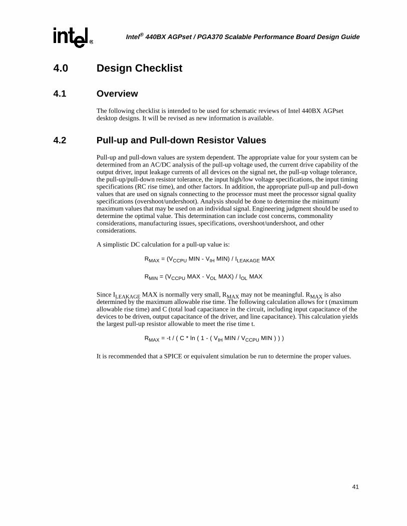
Pull-up and pull-down values are system dependent. The appropriate value for your system can be determined from an AC/DC analysis of the pull-up voltage used, the current drive capability of the output driver, input leakage currents of all devices on the signal net, the pull-up voltage tolerance, the pull-up/pull-down resistor tolerance, the input high/low voltage specifications, the input timing specifications (RC rise time), and other factors. In addition, the appropriate pull-up and pull-down values that are used on signals connecting to the processor must meet the processor signal quality specifications (overshoot/undershoot). Analysis should be done to determine the minimum/maximum values that may be used on an individual signal. Engineering judgment should be used to determine the optimal value. This determination can include cost concerns, commonality considerations, manufacturing issues, specifications, overshoot/undershoot, and other considerations.
A simplistic DC calculation for a pull-up value is:
RMAX = (VCCPU MIN - VIH MIN) / ILEAKAGE MAX
RMIN = (VCCPU MAX - VOL MAX) / IOL MAX
Since ILEAKAGE MAX is normally very small, RMAX may not be meaningful. RMAX is also determined by the maximum allowable rise time. The following calculation allows for t (maximum allowable rise time) and C (total load capacitance in the circuit, including input capacitance of the devices to be driven, output capacitance of the driver, and line capacitance). This calculation yields the largest pull-up resistor allowable to meet the rise time t.
RMAX = -t / ( C * ln ( 1 - ( VIH MIN / VCCPU MIN ) ) )
It is recommended that a SPICE or equivalent simulation be run to determine the proper values.
41

Intel® 440BX AGPset / PGA370 Scalable Performance Board Design Guide
4.3 Processor Checklist
4.3.1 PGA370-Based Processors
Figure 23. Pull-up Resistor Example
Table 17. AGTL+ Connectivity (Sheet 1 of 2)
CPU Pin Pin Connection
A[35:3] A[31:3]: Terminate to VTT / Connect to 82443BXA[35:32]: Leave as NO CONNECT
ADS# Terminate to VTT / Connect to 82443BX
AERR# Leave as NO CONNECT
AP[1:0] Leave as NO CONNECT
BERR# Leave as NO CONNECT
BINIT# Leave as NO CONNECT
BNR# Terminate to VTT / Connect to 82443BX
BP[3:2]# Leave as NO CONNECTOptional Debug: If used, terminate to VTT
BPM[1:0] Leave as NO CONNECTOptional Debug: If used, terminate to VTT
BPRI# Terminate to VTT / Connect to 82443BX
BR[0]# Terminate to VTT / Connect to 82443BX pin BREQ#Optional: connect to ground with a 10 Ω resistor
D[63:0]# Terminate to VTT / Connect to 82443BX
DBSY# Terminate to VTT / Connect to 82443BX
DEFER# Terminate to VTT / Connect to 82443BX
DEP[7:0] Leave as NO CONNECT
VccPU MIN
RMAX
VIH MINILEAKAGE MAX
VccPU MAX
RMin
VOL MAXIOL MAX
v009.vsd
42

Intel® 440BX AGPset / PGA370 Scalable Performance Board Design Guide
DRDY# Terminate to VTT / Connect to 82443BX
HIT# Terminate to VTT / Connect to 82443BX
HITM# Terminate to VTT / Connect to 82443BX
LOCK# Terminate to VTT / Connect to 82443BX
REQ[4:0]# Terminate to VTT / Connect to 82443BX
RESET# Terminate to VTT / Connect to 82443BX. See Section 3.2.4, “AGTL+ Reset Implementation” on page 38.
RESET2# Driven by same signal as RESET#. See Section 3.2.4, “AGTL+ Reset Implementation” on page 38.
RP# Leave as NO CONNECT
RS[2:0]# Terminate to VTT / Connect to 82443BX
RSP# Leave as NO CONNECT
TRDY# Terminate to VTT / Connect to 82443BX
Table 18. CMOS Connectivity
CPU Pin Pin Connection
A20M# Pull-up to VCCCMOS with a ~280 Ω resistor. Connect to PIIX4E.
FERR#Pull-up to VCCCMOS with a 1.5 KΩ resistor. Connect to PIIX4E via the voltage conversion logic. See Section 3.2.5, “CMOS Voltage Conversion Logic” on page 40
FLUSH# Pull-up to VCCCMOS with a ~280 Ω resistor.
IERR# Leave as NO CONNECTOptional: Pull-up to VCCCMOS with a ~280 Ω resistor and connect to error logic
IGNNE# Pull-up to VCCCMOS with a ~280 Ω resistor. Connect to PIIX4E.
INIT# Pull-up to VCCCMOS with a ~280 Ω resistor. Connect to PIIX4E.
LINT[1] / NMI Pull-up to VCCCMOS with a ~280 Ω resistor. Connect to PIIX4E.
LINT[0] / INTR Pull-up to VCCCMOS with a ~280 Ω resistor. Connect to PIIX4E.
PICD[1:0] Pull-up to VCCCMOS with a ~200-330 Ω resistor.
PREQ# Pull up to VCCCMOS with a ~200-330 Ω resistor. Optional debug; connect to ITP.
PWRGOOD Pull-up to VCC2.5 with a ~200-330 Ω resistor. Connect to power sense logic.
SLP# Pull-up to VCCCMOS with a ~280 Ω resistor. Connect to PIIX4E.
SMI# Pull-up to VCCCMOS with a ~280 Ω resistor. Connect to PIIX4E.
STPCLK# Pull-up to VCCCMOS with a ~280 Ω resistor. Connect to PIIX4E.
THERMTRIP#NO CONNECT. Optional: pull-up to VCCCMOS with a 1.5 KΩ resistor. Connect to error logic via the voltage conversion logic. See Section 3.2.5, “CMOS Voltage Conversion Logic” on page 40.
Table 17. AGTL+ Connectivity (Sheet 2 of 2)
CPU Pin Pin Connection
43

Intel® 440BX AGPset / PGA370 Scalable Performance Board Design Guide
Table 19. TAP Connectivity (optional)
CPU Pin Pin Connection
PRDY# 56 Ω pull up to VTT, 240 Ω series resistor to ITP connector
TCK 1 KΩ pull-up to VCCCMOS. 47 Ω series resistor to ITP connector
TDO Connected to ITP/processor. 150 Ω pull-up to VCCCMOS
TDI Connected to ITP/processor. ~200-330 Ω pull-up to VCCCMOS
TMS 1 KΩ pull-up to VCCCMOS. 47 Ω series resistor to ITP connector
TRST# Connect to ITP/processor. 650 Ω pull-down
NOTE: If not used, connect TCK, TD1, TMS, and TRST# to valid logic level; do not leave floating.
Table 20. Clock Connectivity
CPU Pin Pin Connection
BCLK Connect to CK100. Gang with 82443BX HCLK. Tune the 33 Ω series resistor for signal integrity.
PICCLK Connect to CK100. Tune the 33 Ω series resistor for signal integrity.
Table 21. Miscellaneous Connectivity
CPU Pin Pin Connection
BSEL0 Pull-up to VCC3.3 with a 1 KΩ resistor. Connect to CK100 SEL100/66# input, Connect to 82443BX via 10 K Ω resistor. See Section 3.2.2, “BSEL[1:0] Implementation” on page 36.†
BSEL1 1 KΩ resistor pull down to GND
CPUPRES# Tie to GND. Optionally pull-up for external logic.
EDGCTRL Pull-up to VCCCORE with a 51 Ω ± 5% resistor
RTTCTRL 110 Ω 1% pull down to GND
SLEWCTRL 110 Ω 1% pull down to GND
THERMDN NO CONNECT if not used
THERMDP NO CONNECT if not used
VCOREDET Leave as NO CONNECT
VID[3:0] 10 KΩ pull-up to 5 V; connect to VRM.
VID[4] Not on processor. Connect VRM controller pin to GND.
† The Celeron processor datasheet states that BSEL0 is a 2.5 V tolerant pin. For Celeron processors with a 66 MHz processor system bus, BSEL0 is not bonded out; pulling the signal up to 3.3 V has no effect on processor operation.
44

Intel® 440BX AGPset / PGA370 Scalable Performance Board Design Guide
4.3.2 GND and Power Pin Definition
Refer to the Celeron processor and Intel 440BX datasheets, and to the Pentium® III Processor for the PGA370 Socket datasheet for this information.
4.3.3 Processor Clocks
• PICCLK must be driven by a clock even if an I/O APIC is not being used. This clock can be as high as 33.3 MHz in a uniprocessor system.
Table 22. Power Connectivity
CPU Pin Pin Connection
CLKREF
Board divider on VCC2.5 or VCC3.3 to create 1.25 V reference with a 4.7 µF decoupling capacitor. Resistor divider must be created from 1% tolerance resistors. Do not use VTT as source voltage for this reference!. See Section 3.2.3, “CLKREF Circuit Implementation” on page 37.
PLL1 & PLL2
Low pass filter on VCCCORE provided on board. Typically a 4.7 µH inductor in series with VCCCORE is connected to PLL1 then through a series 33 µF capacitor to PLL2. See Section 1.5.7, “Phase Lock Loop (PLL) Power” on page 12 for inductor and capacitor values.
VCC1.5 Connect to 1.5 V supply
VCC2.5 Connect to 2.5 V supply
VCCCMOS Use for system CMOS pull-up voltage. Provide 0.1 µF decoupling
VCCCORE
Connect to VRM output/
Decoupling Guidelines:10 (min) 4.7 µF in 1206 package
VREF[7:0]
Connect to VREF voltage divider made up of 75 Ω ± 1% and 150 Ω ± 1% resistors connected to VTT.
Decoupling Guidelines:4 (min) 0.1 µF in 0603 package
VSS Tie to GND
VTT
Connect AH20, AK16, AL13, AL21, AN11, AN15, and G35 to 1.5 V regulator.
Decoupling Guidelines:19 (min) 0.1 µF in 0603 package placed within 200 mils of AGTL+ termination resistor packs. Use one capacitor for every two rpacks.
Table 23. No Connects
CPU Pin Pin Connection
VTTThe following pins must be left as NO CONNECTS: AA33, AA35, AN21, E23, S33, S37, U35, U37.
Reserved The following pins must be left as NO CONNECTS: AK30, AM2, F10, G37, L33, N33, N35, N37, Q33, Q35, Q37, R2, W35, X2, Y1.
45

Intel® 440BX AGPset / PGA370 Scalable Performance Board Design Guide
t
D”
4.3.4 Processor Signals
• THERMTRIP# must be pulled-up to VCCCMOS (1.5 KΩ) if used by system logic via the voltage conversion logic as shown in Figure 22. The signal may be wire-OR’ed and does norequire an external gate. It may be left as NO CONNECT if it is not used.
• The FERR# output must be pulled up to VCCCMOS (1.5 KΩ) and connected to the PIIX4E via the voltage conversion logic as shown in Figure 22. Please see the reference schematics.
• PICD[1:0] must have ~200-330 Ω pull-ups to VCCCMOS even if an I/O APIC is not being used.
• All CMOS inputs should be pulled up to VCCCMOS with appropriate resistor value.
• The processor inputs should not be driven by 2.5 V, 3.3 V, or 5 V logic. Logic translation of 2.5 V, 3.3 V, or 5 V signals may be accomplished by using open-drain drivers pulled-up to VCCCMOS.
• The PWRGOOD input should be driven to the appropriate level from the active-high “ANof the “Power Good” signals from the 5 V, 3.3 V, and VCCCORE supplies. The output of any logic used to drive PWRGOOD should be a 2.5 V level to the processor.
• VREF should be generated for the processor. Intel recommends using a 75 Ω ± 1% and 150Ω ± 1% resistor divider with VTT for generating VREF. VREF is not locally generated on the processor as it is on the S.E.P. package.
• VTT must have adequate bulk decoupling based on the reaction time of the regulator used to generate VTT. The regulator must provide for a current ramp of up to 8 A/ms while maintaining the voltage tolerance defined in the Intel® Celeron™ Processor datasheet and the Pentium® III Processor for the PGA370 Socket datasheet. In addition, VTT must have adequate high-frequency decoupling on the system board. See decoupling guidelines.
• If an on-board voltage regulator is used instead of a VRM, VCCCORE must have adequate bulk decoupling based on the reaction time of the regulator used to generate VCCCORE. The regulator must provide for a current ramp of up to 20 A/µs while maintaining compliance withthe VRM 8.4 DC-DC Converter Design Guidelines.
• The VID lines should have pull-up resistors on them ONLY if they are required by the Voltage Regulator Module or on-board regulator used. The pull-up voltage used should be to the regulator input voltage (5 V or 12 V); however, if 12 V is used, a resistor divider should be utilized to lower the VID signal to CMOS/TTL levels. A pull-up is not required unless the VID signals are used by other logic requiring CMOS/TTL logic levels. The VID lines on the processor are 5 V tolerant.
• The TAP port must be properly terminated even if it is not used.
• TRST# must be driven low during reset to all components with TRST# pins. Connecting a pull-down resistor to TRST# will accomplish the reset of the port. See the figures in the Integration Tools chapter of the P6 Family Processors Developer’s Manual.
• A single VTT regulator may be used. A simplistic, single-ended termination, calculation for maximum worst case current is 2.7 A. This takes into consideration that some signals are not used by the Intel 440BX AGPset.
• Boards planning to support the boxed processor must provide a matched power header for the boxed processor fan/heatsink power cable connector. Consult the Intel® Celeron™ Processor datasheet for specifications for the fan power cable connector. The power header must be positioned close to the PGA370 socket.
• The CPUPRES# signal is a ground on the processor. The presence of a CPU core can be determined with this pin if it is pulled up on the system board. If not used, connect to ground to provide additional support to the processor.
• DBRESET (ITP Reset signal) requires a 240 Ω pull-up to VCC3.3.
46

Intel® 440BX AGPset / PGA370 Scalable Performance Board Design Guide
ectly rall
f
• The system board should connect the processor’s BR0# signal to the BREQ0# signal on the82443BX. This assigns an agent ID of 0 to the processor. Optionally, this signal may be grounded with a 10Ω resistor.
4.3.5 Processor Decoupling Capacitors
4.3.5.1 Core Voltage High-Frequency Decoupling
• Intel recommends ten or more 4.7 µF capacitors in a 1206 package, 19 or more 1.0 µF in a0805 package. All capacitors should be placed within the socket cavity and mounted diron the primary side of the board. The capacitors should be arranged to minimize the oveinductance between VCC/VSS power pins (See Figure 24).
• Contact your regulator vendor for bulk decoupling recommendations that meet the VRM 8.4 DC-DC Converter Guidelines.
• Decoupling capacitor traces should be as short and wide as possible.
• The VRM 8.4 regulator provides the scalable performance board PGA370 socket guidelines for processor voltage and current.
4.3.5.2 VTT Decoupling
• Intel recommends 19 or more 0.1 µF in a 0603 package placed within 200 mils of R-packs,one capacitor for every two R-packs. These capacitors are shown on the outer exterior oFigure 24. These are located on the board.
Figure 24. Example Capacitor Placement Within the PGA370 Socket
47

Intel® 440BX AGPset / PGA370 Scalable Performance Board Design Guide
e to the ith
4.3.5.3 VREF Decoupling
• Intel recommends four or more 0.1 µF in a 0603 package placed near VREF pins (within 500 mils).
4.4 Board Component Keep-Out
The Keep-Out area represents space where the board component placement is restricted ducombined effect of all thermal solution components. The board component Keep-Out area wcomponent height restrictions is shown in Figure 25.
Figure 25. Board Component Keep-Out
PGA 370 & PGA370S
All dimensions are minimum unless otherwise specified
No components
0 . 122" Max. Height Off MB
EMI Pads
0 . 060" Max. Height Off MB
0 . 127" Max. Height Off MB
1 . 022" Max. Height Off MB
1 . 38
2 . 528 . 005REF .PGA370DESIGNSPEC.
1 . 44
1 . 44
1 . 54
1 . 83
4X . 400 4X . 450
4X . 175
4X . 258
. 210 . 672
+ -
1 . 570 1 . 570
1.315 NOM 1.315 NOM 1 . 68
. 672. 290
48

Intel® 440BX AGPset / PGA370 Scalable Performance Board Design Guide
4.5 Thermals/Cooling Solutions
• For the PGA-370 based processors, an adequate heat sink and air ventilation must be provided to ensure that the TCASE/TJUNCTION specifications are met. These specifications can be found in the Intel® Celeron™ Processor datasheet and the Pentium® III Processor for the PGA370 Socket datasheet. For additional thermal information, refer to Intel® Pentium® III Processor Thermal Metrology for CPUID 068xh Family Processors.
• The scalable performance board guidelines for processor power dissipation is 27 W at a TCASE of 70o C for PPGA processors, and 26.7 W at a TJ of 80 oC for FC-PGA processors.
• Verify that all major components, including the 82443BX can be cooled given the way they are placed.
4.5.1 Thermal Solution Design Considerations
The following questions should be considered when implementing the thermal solution.
• Could anything block the airflow to or from the processor (I/O cards, VRM etc.)?
• Is there anything between the processor and the air intake that may preheat the air flowing into the fan/heatsink?
• If a system fan (other than the power supply fan) is used, have all recirculation paths been eliminated?
• What is the air flow through the PSU/system fan?
• What is the maximum ambient operation temperature of the system?
4.6 Mechanical Design Considerations
• For the processor: The physical space requirements of the processor must be met. See the Intel® Celeron™ Processor datasheet and the Pentium® III Processor for the PGA370 Socket datasheet for details. In addition, the physical space requirements of your heatsink must be met.
• For the boxed processor: The physical space requirements of the boxed processor fan/heatsink must be met. See the Intel® Celeron™ Processor datasheet and the Pentium® III Processor for the PGA370 Socket datasheet for details.
49

Intel® 440BX AGPset / PGA370 Scalable Performance Board Design Guide
4.7 Electrical Design Considerations
• It is recommended that simulations be performed on the AGTL+ bus to ensure that proper bus timings and signal integrity are met, especially if the layout recommendations in this document are not followed.
• It is recommended that simulations be performed to ensure that proper signal integrity is met on the non-AGTL+ (CMOS) signals.
• Verify that the voltage range and tolerance of your VRM or on-board regulator adequately cover the VCCCORE requirements of the PGA370-based processors.
• The maximum current value your VRM or on-board regulator can support at VCCCORE should meet the value specified by the VRM 8.4 DC-DC Converter Guidelines.
• The voltage tolerance of your VRM or on-board regulator at VCCCORE should meet the value specified by the VRM 8.4 DC-DC Converter Guidelines.
• Adequate 5 V and/or 3.3 V decoupling should be provided for all components.
• VREF for the AGPset should be decoupled to VTT with 0.001 µF capacitors at each voltage divider. It should be decoupled to ground to ensure a better solution.
• It is recommended that AC/DC and signal integrity analysis be performed to determine proper pull-up and pull-down values.
50

Intel® 440BX AGPset / PGA370 Scalable Performance Board Design Guide
igns
5.0 Third-Party Vendor Information
This section refers to listings of various third-party vendors who provide products to support the PGA-370-based processors and the Intel 440BX AGPset. The lists of vendors can be used as a starting point for the designer. Intel does not endorse any one vendor or guarantee the availability or functionality of outside components. Contact the manufacturer for specific information regarding performance, availability, pricing, and compatibility.
5.1 Voltage Regulator Control Silicon
Intel’s Developer website lists vendors who offer DC-DC converter silicon and reference desthat meet the Celeron and PentiumIII processor voltage and current requirements:
http://developer.intel.com/design/celeron/components/#POWER.
5.2 Clock Drivers
Intel’s Developer website lists vendors who offer clock drivers for the Celeron and the PentiumIII processors and Intel 440BX AGPset.
http://developer.intel.com/design/celeron/components/#CLOCK.
5.3 PGA370 Socket
The PGA370 Socket Guidelines document can be obtained from:
http://developer.intel.com/design/celeron/applnots/244410.htm
51


Intel® 440BX AGPset / PGA370 Scalable Performance Board Design Guide
Index
440BX AGPset features 982443BX BGA pins 16
AAC guidelines
system bus 32AGTL+
description 21pin connection checklist 42RESET signal 38, 39signal integrity 50signals 22simulations 23termination 11
ATX form factor 18
BBGA pins 16Board
impedance 20keep-out area 48layout rules 22routing guidelines 21stack-up 20topology 21
boarddescription 20
Boxed processors 10BSEL 36Bus frequency selection 15
CCeleron processor
design checklist 42CLKREF 37Clocks
host clock routing 27host clock topology 29pin connections 44processor clock design guidelines 45system clock layout 28
CMOS design guidelines 11CMOS pin connections 43CMOS voltage conversion 40Crosstalk 25
DDC guidelines
for PGA370-based processors 30
Decoupling 50Decoupling capacitors 47Design considerations
electrical 50mechanical 49
Design recommendations-general 10Discrete R 15Documents-related 8
EElectrical design considerations 50
FFlight time simulation 24
HHost clock
routing 27topology 29
IImpedance on board 20Intel 440BX AGPset features 9
KKeep-out area 48
LLayout, board 22
MMechanical design considerations 49Multi-bit timing adjustment factor 25
NNew pins 15NLX form factor 19Notation 7
PParametric sweeps 23PGA370-based processors
53

Intel® 440BX AGPset / PGA370 Scalable Performance Board Design Guide
design features 9pins 17socket design 36voltage specs 30
Pin connectionsCeleron processor 42–45
Pinsnew for PGA370 15
PLL filterrecommendation 14specification 13topology 12
Power-on timings 35Pull-up/pull-down resistors 41
RRelated documents 8Routing guidelines board 21
SSC-242 socket
transitioning from 11Signal quality
measurement 25Signals
AGTL+ RESET 38, 39BSEL 36CLKREF 37processor signal guidelines 46
Simulationflight time 24methodology 23
post-layout 25pre-layout 23
Socket design 36Stack-up
board guidelines 20system board 20
System board description 20System bus
AC guidelines 32timing diagrams 34
System clock layout 28
TTAP pin connections 44Terminology 7Thermal guidelines 35Thermal solutions 49Third-party vendors 51Timing analysis 26Topology
AGTL+ bus 22board 21
Trace lengths 22
VVoltage decoupling 12Voltage definitions 10Voltage ID pin 12Voltage Regulator Module 10Voltages-PGA370-based processors 30VRM guidelines 50
54