intel® advanced+ boot block flash memory (c3) scsp family ... sheets/intel pdfs/28f160xc3,...
TRANSCRIPT

Order Number: 252636, Revision: 00426 Aug 2005
Intel® Advanced+ Boot Block Flash Memory (C3)SCSP Family
Datasheet
Product Features
The Intel® Advanced+ Boot Block Flash Memory (C3) Stacked Chip Scale Package (SCSP) device delivers a feature-rich solution for low-power applications. The C3 SCSP memory device incorporates flash memory and static RAM in one package with low voltage capability to achieve the smallest system memory solution form-factor together with high-speed, low-power operations. The C3 SCSP memory device offers a protection register and flexible block locking to enable next generation security capability. Combined with the Intel® Flash Data Integrator (Intel® FDI) software, the C3 SCSP memory device provides a cost-effective, flexible, code plus data storage solution.
Flash Memory Plus SRAM—Reduces Memory Board Space
Required, Simplifying PCB Design Complexity
SCSP Technology—Smallest Memory Subsystem Footprint
—Area : 8 x 10 mm for 16 Mbit (0.13 µm) Flash + 2 Mbit or 4 Mbit SRAM
—Area : 8 x 12 mm for 32 Mbit (0.13 µm) Flash + 4 Mbit or 8 Mbit SRAM
—Height : 1.20 mm for 16 Mbit (0.13 µm) Flash + 2 Mbit or 4 Mbit SRAM, and 32 Mbit (0.13um) Flash + 8 Mbit SRAM
—Height : 1.40 mm for 32 Mbit (0.13 µm) Flash + 4 Mbit SRAM
—This Family also includes 0.25 µm, 0.18 µm, and 0.13 µm technologies
Advanced SRAM Technology—70 ns Access Time
—Low Power Operation
—Low Voltage Data Retention Mode
Intel® Flash Data Integrator (FDI) Software —Real-Time Data Storage and Code
Execution in the Same Memory Device
—Full Flash File Manager Capability
Advanced+ Boot Block Flash Memory—70 ns Access Time
—Instant, Individual Block Locking
—128 bit Protection Register
—12 V Production Programming
—Fast Program and Erase Suspend
—Extended Temperature –25 °C to +85 °C
Blocking Architecture—Block Sizes for Code + Data Storage
—4-Kword Parameter Blocks
—64-Kbyte Main Blocks
—100,000 Erase Cycles per Block
Low Power Operation—Asynchronous Read Current: 9 mA
(Flash)
—Standby Current: 7 µA (Flash)
—Automatic Power Saving Mode
Flash Technologies—0.25 µm ETOX™ VI, 0.18 µm ETOX™
VII and 0.13 µm ETOX™ VIII Flash Technologies

26 Aug 2005 Intel® Advanced+ Boot Block Flash Memory (C3) SCSP Family Datasheet2 Order Number: 252636, Revision: 004
INFORMATION IN THIS DOCUMENT IS PROVIDED IN CONNECTION WITH INTEL® PRODUCTS. EXCEPT AS PROVIDED IN INTEL’S TERMS AND CONDITIONS OF SALE FOR SUCH PRODUCTS, INTEL ASSUMES NO LIABILITY WHATSOEVER, AND INTEL DISCLAIMS ANY EXPRESS OR IMPLIED WARRANTY RELATING TO SALE AND/OR USE OF INTEL PRODUCTS, INCLUDING LIABILITY OR WARRANTIES RELATING TO FITNESS FOR A PARTICULAR PURPOSE, MERCHANTABILITY, OR INFRINGEMENT OF ANY PATENT, COPYRIGHT, OR OTHER INTELLECTUAL PROPERTY RIGHT.
Intel Corporation may have patents or pending patent applications, trademarks, copyrights, or other intellectual property rights that relate to the presented subject matter. The furnishing of documents and other materials and information does not provide any license, express or implied, by estoppel or otherwise, to any such patents, trademarks, copyrights, or other intellectual property rights.
Intel products are not intended for use in medical, life saving, life sustaining, critical control or safety systems, or in nuclear facility applications.
Intel may make changes to specifications and product descriptions at any time, without notice.
The Intel® Advanced+ Boot Block Flash Memory (C3) may contain design defects or errors known as errata which may cause the product to deviate from published specifications. Current characterized errata are available on request.
Contact your local Intel sales office or your distributor to obtain the latest specifications and before placing your product order.
Copies of documents which have an ordering number and are referenced in this document, or other Intel literature may be obtained by calling 1-800-548-4725 or by visiting Intel's website at http://www.intel.com.
Intel, the Intel logo, Intel StrataFlash, and ETOX are trademarks or registered trademarks of Intel Corporation or its subsidiaries in the United States and other countries.
*Other names and brands may be claimed as the property of others.
Copyright © 2005, Intel Corporation. All rights reserved.

C3 SCSP Flash Memory
Datasheet Intel® Advanced+ Boot Block Flash Memory (C3) SCSP Family 26 Aug 2005Order Number: 252636, Revision: 004 3
Contents1.0 Introduction....................................................................................................................................6
1.1 Document Conventions ........................................................................................................61.2 Product Overview .................................................................................................................61.3 Package Ballout ....................................................................................................................81.4 Signal Definitions ..................................................................................................................9
2.0 Principles of Operation ...............................................................................................................11
2.1 Bus Operation.....................................................................................................................112.1.1 Read ......................................................................................................................122.1.2 Output Disable .......................................................................................................122.1.3 Standby..................................................................................................................132.1.4 Flash Reset............................................................................................................132.1.5 Write ......................................................................................................................13
3.0 Flash Memory Modes of Operation............................................................................................14
3.1 Read Array (FFh)................................................................................................................143.2 Read Identifier (90h) ...........................................................................................................143.3 Read Status Register (70h) ................................................................................................15
3.3.1 Clear Status Register (50h) ...................................................................................163.4 CFI Query (98h)..................................................................................................................163.5 Word Program (40h/10h) ....................................................................................................16
3.5.1 Suspending and Resuming Program (B0h/D0h)....................................................173.6 Block Erase (20h) ...............................................................................................................18
3.6.1 Suspending and Resuming Erase (B0h/D0h)........................................................183.7 Block Locking......................................................................................................................20
3.7.1 Block Locking Operation Summary........................................................................213.7.2 Locked State..........................................................................................................213.7.3 Unlocked State ......................................................................................................213.7.4 Lock-Down State ...................................................................................................213.7.5 Reading Lock Status for a Block............................................................................223.7.6 Locking Operation During Erase Suspend ............................................................223.7.7 Status Register Error Checking .............................................................................22
3.8 128 Bit Protection Register .................................................................................................233.8.1 Reading the Protection Register ............................................................................233.8.2 Programming the Protection Register (C0h)..........................................................243.8.3 Locking the Protection Register .............................................................................24
4.0 Power and Reset Considerations ..............................................................................................25
4.1 Power-Up/Down Characteristics .........................................................................................254.2 Additional Flash Features ...................................................................................................25
4.2.1 Improved 12 Volt Production Programming ...........................................................254.2.2 F-VPP £ VPPLK for Complete Protection ..............................................................25
5.0 Electrical Specifications .............................................................................................................26
5.1 Absolute Maximum Ratings ................................................................................................265.2 Operating Conditions ..........................................................................................................275.3 Capacitance........................................................................................................................27

C3 SCSP Flash Memory
26 Aug 2005 Intel® Advanced+ Boot Block Flash Memory (C3) SCSP Family Datasheet4 Order Number: 252636, Revision: 004
5.4 DC Characteristics.............................................................................................................. 285.5 Flash AC Characteristics. ................................................................................................... 325.6 Flash AC Characteristics—Write Operations......................................................................335.7 Flash Erase and Program Timings(1)................................................................................. 345.8 Flash Reset Operations...................................................................................................... 365.9 SRAM AC Characteristics—Read Operations....................................................................375.10 SRAM AC Characteristics—Write Operations ....................................................................385.11 SRAM Data Retention Characteristics—Extended Temperature ....................................... 40
6.0 Migration Guide Information ...................................................................................................... 41
7.0 System Design Considerations.................................................................................................. 41
7.1 Background......................................................................................................................... 417.1.1 Flash + SRAM Footprint Integration ......................................................................417.1.2 C3 Flash Memory Features ................................................................................... 42
7.2 Flash Control Considerations ............................................................................................. 427.2.1 F-RP# Connected to System Reset....................................................................... 427.2.2 F-VCC, F-VPP and F-RP# Transition ....................................................................42
7.3 Noise Reduction .................................................................................................................437.4 Simultaneous Operation .....................................................................................................44
7.4.1 SRAM Operation during Flash “Busy” ................................................................... 457.4.2 Simultaneous Bus Operations ............................................................................... 45
7.5 Printed Circuit Board Notes ................................................................................................ 457.6 System Design Notes Summary.........................................................................................45
A Program/Erase Flowcharts ............................................................................................................46
B CFI Query Structure ...................................................................................................................... 52
B.1 Query Structure Output....................................................................................................... 52B.2 Query Structure Overview .................................................................................................. 53B.3 Block Lock Status Register................................................................................................. 54B.4 CFI Query Identification String............................................................................................ 54B.5 System Interface Information..............................................................................................55B.6 Device Geometry Definition................................................................................................ 56B.7 Intel-Specific Extended Query Table ..................................................................................57
C Word-Wide Memory Map Diagrams ..............................................................................................59
D Device ID Table............................................................................................................................. 66
E Protection Register Addressing .....................................................................................................67
F Mechanical and Shipping Media Details........................................................................................ 68
F.8 Mechanical Specification .................................................................................................... 68F.9 Media Information............................................................................................................... 71
G Additional Information.................................................................................................................... 73
H Ordering Information...................................................................................................................... 74

C3 SCSP Flash Memory
Datasheet Intel® Advanced+ Boot Block Flash Memory (C3) SCSP Family 26 Aug 2005Order Number: 252636, Revision: 004 5
Revision History
Date of Revision Version Description
02/11/03 -001 Initial release, Stacked Chip Scale Package
01/29/04 -002 Minor text edits.
03/05 -003 Updated Ordering Information figures and table in Appendix H.
26 Aug 2005 -004 Updated Ordering Information to add PF28F1602C3TD70.

C3 SCSP Flash Memory
26 Aug 2005 Intel® Advanced+ Boot Block Flash Memory (C3) SCSP Family Datasheet6 Order Number: 252636, Revision: 004
1.0 Introduction
This document contains the specifications for the Intel® Advanced+ Boot Block Flash Memory (C3) Stacked Chip Scale Package (SCSP) device. C3 SCSP memory solutions are offered in the following combinations:
• 32-Mbit flash + 8-Mbit SRAM
• 32-Mbit flash + 4-Mbit SRAM
• 16-Mbit flash + 4-Mbit SRAM
• 16-Mbit flash memory + 2-Mbit SRAM
1.1 Document Conventions
Throughout this document, the following conventions have been adopted.
• Voltages:
— 2.7 V refers to the full voltage range, 2.7 V–3.3V
— 12 V refers to 11.4 V to 12.6 V
• Main block(s): 32-Kword block
• Parameter block(s): 4-Kword block
1.2 Product Overview
The C3 SCSP device combines flash memory and SRAM into a single package, which provides secure low-voltage memory solutions for portable applications.
The flash memory provides the following features:
• Enhanced security.
• Instant locking/unlocking of any flash block with zero-latency
• A 128-bit protection register that enables unique device identification, to meet the needs of next generation portable applications.
• Improved 12 V production programming for increased factory throughput.
Table 1. Block Organization (x16)
Memory Device Kwords
32-Mbit Flash 2048
16-Mbit Flash 1024
2-Mbit SRAM 128
4-Mbit SRAM 256
8-Mbit SRAM 512
Note: All words are 16 bits each.
C3 SCSP Flash Memory
Datasheet Intel® Advanced+ Boot Block Flash Memory (C3) SCSP Family 26 Aug 2005Order Number: 252636, Revision: 004 7
The flash memory is asymmetrically-blocked to enable system integration of code and data storage in a single device. Each flash block can be erased independently of the others up to 100,000 times.
The flash memory has eight 8-KB parameter blocks located at either the top (denoted by -T suffix) or the bottom (-B suffix) of the address map, to accommodate different microprocessor protocols for kernel code location.
The remaining flash memory is grouped into 32-Kword main blocks.
Any individual flash memory block can be locked or unlocked instantly to provide complete protection for code or data (see Section 5.7, “Flash Erase and Program Timings(1)” on page 34 for details).
The flash memory contains both a Command User Interface (CUI) and a Write State Machine (WSM).
• The CUI is the interface between the microcontroller and the internal operation of the flash memory.
• The internal WSM automatically executes the algorithms and timings necessary for program and erase operations, including verification, thereby unburdening the microprocessor or microcontroller. To indicate the status of the WSM, the flash memory status register signifies block erase or word program completion and status.
Flash program and erase automation enables executing program and erase operations using an industry-standard two-write command sequence to the CUI.
• Program operations are performed in word increments.
• Erase operations erase all locations within a block simultaneously.
The system software can suspend both program and erase operations to read from any other flash block. In addition, data can be programmed to another flash block during an erase suspend.
The C3 SCSP memory device offers two low-power savings features to significantly reduce power consumption:
• Automatic Power Savings (APS) for flash memory. The C3 SCSP memory device automatically enters APS mode after a read cycle completes from the flash memory.
• Standby mode for flash and SRAM. This mode is initiated when the system deselects the device by driving F-CE# and S-CS1# or S-CS2 inactive.
To reset the flash memory, lower the F-RP# signal to GND. Setting F-RP# to GND provides CPU memory reset synchronization and additional protection against bus noise that can occur during system reset and power-up/power-down sequences.

C3 SCSP Flash Memory
26 Aug 2005 Intel® Advanced+ Boot Block Flash Memory (C3) SCSP Family Datasheet8 Order Number: 252636, Revision: 004
1.3 Package Ballout
72-
Notes:1. Flash memory upgrade balls are shown up to A21 (64-Mbit flash) and A22 (128-Mbit flash). In all flash
memory and SRAM combinations, 66 balls are populated on lower density devices. (Upper address balls are not populated). Ball location A10 is NC on 16/2 devices only.
2. To maintain compatibility with all JEDEC Variation B options for the C6 ball location, connect this C6 land pad directly to the land pad for the G4 (A17) ball.
Figure 1. 66-Ball SCSP Package Ballout
1 2 3 4 5 6 7 8
A
B
C
D
E
F
G
H
NC A20 A11 A15 A14 A13 A12
A16 A8 A10 A9 DQ15 S-WE#
F-WE# NC A21 DQ13 DQ6
S-VSS
F-WP# A19 DQ11 DQ10
S-LB# S-UB# S-OE# DQ9 DQ8
A18 A17 A7 A6 A3 A2
NC NC A5 A4 A0 F-CE# F-VSS
F-RP# A22 DQ12 S-CS2
9 10 11 12
F-VSS NC
DQ14DQ7
DQ4 DQ5
DQ2 DQ3
DQ0 DQ1
A1 S-CS1#
F-OE# NC NC
S-VCC F-VCC
Top View, Balls Down
F-VCCQ
F-VPP
C3 SCSP Flash Memory
Datasheet Intel® Advanced+ Boot Block Flash Memory (C3) SCSP Family 26 Aug 2005Order Number: 252636, Revision: 004 9
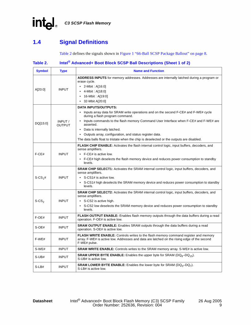
1.4 Signal Definitions
Table 2 defines the signals shown in Figure 1 “66-Ball SCSP Package Ballout” on page 8.
Table 2. Intel® Advanced+ Boot Block SCSP Ball Descriptions (Sheet 1 of 2)
Symbol Type Name and Function
A[20:0] INPUT
ADDRESS INPUTS for memory addresses. Addresses are internally latched during a program or erase cycle.
• 2-Mbit : A[16:0]
• 4-Mbit : A[18:0]
• 16-Mbit : A[19:0]
• 32-Mbit A[20:0]
DQ[15:0] INPUT / OUTPUT
DATA INPUTS/OUTPUTS:
• Inputs array data for SRAM write operations and on the second F-CE# and F-WE# cycle during a flash program command.
• Inputs commands to the flash memory Command User Interface when F-CE# and F-WE# are asserted.
• Data is internally latched.
• Outputs array, configuration, and status register data.
The data balls float to tristate when the chip is deselected or the outputs are disabled.
F-CE# INPUT
FLASH CHIP ENABLE: Activates the flash internal control logic, input buffers, decoders, and sense amplifiers.
• F-CE# is active low.
• F-CE# high deselects the flash memory device and reduces power consumption to standby levels.
S-CS1# INPUT
SRAM CHIP SELECT1: Activates the SRAM internal control logic, input buffers, decoders, and sense amplifiers.
• S-CS1# is active low.
• S-CS1# high deselects the SRAM memory device and reduces power consumption to standby levels.
S-CS2 INPUT
SRAM CHIP SELECT2: Activates the SRAM internal control logic, input buffers, decoders, and sense amplifiers.
• S-CS2 is active high.
• S-CS2 low deselects the SRAM memory device and reduces power consumption to standby levels.
F-OE# INPUT FLASH OUTPUT ENABLE: Enables flash memory outputs through the data buffers during a read operation. F-OE# is active low.
S-OE# INPUT SRAM OUTPUT ENABLE: Enables SRAM outputs through the data buffers during a read operation. S-OE# is active low.
F-WE# INPUTFLASH WRITE ENABLE: Controls writes to the flash memory command register and memory array. F-WE# is active low. Addresses and data are latched on the rising edge of the second F-WE# pulse.
S-WE# INPUT SRAM WRITE ENABLE: Controls writes to the SRAM memory array. S-WE# is active low.
S-UB# INPUT SRAM UPPER BYTE ENABLE: Enables the upper byte for SRAM (DQ8–DQ15).S-UB# is active low.
S-LB# INPUT SRAM LOWER BYTE ENABLE: Enables the lower byte for SRAM (DQ0–DQ7).S-LB# is active low.

C3 SCSP Flash Memory
26 Aug 2005 Intel® Advanced+ Boot Block Flash Memory (C3) SCSP Family Datasheet10 Order Number: 252636, Revision: 004
F-RP# INPUT
FLASH RESET/DEEP POWER-DOWN: Uses two voltage levels (VIL, VIH) to control reset/deep power-down mode.
• When F-RP# is at logic low, the device is in reset/deep power-down mode, which drives the outputs to High-Z, resets the Write State Machine, and minimizes current levels (ICCD).
• When F-RP# is at logic high, the device is in standard operation.
• When F-RP# transitions from logic-low to logic-high, the device resets all blocks to locked and defaults to the read array mode.
F-WP# INPUT
FLASH WRITE PROTECT: Controls the lock-down function of the flexible Locking feature.
• When F-WP# is a logic low, the lock-down mechanism is enabled and blocks marked lock-down cannot be unlocked through software. After F-WP# goes low, any blocks previously marked lock-down revert to that state.
• When F-WP# is logic high, the lock-down mechanism is disabled. Blocks previously locked-down are now locked, and can be unlocked or locked through software.
See Section 7.0, “System Design Considerations” on page 41 for details on block locking.
F-VCC SUPPLY FLASH POWER SUPPLY: [2.7 V–3.3 V] Supplies power for device core operations.
F-VCCQ SUPPLY FLASH I/O POWER SUPPLY: [2.7 V–3.3 V] Supplies power for device I/O operations.
S-VCC SUPPLYSRAM POWER SUPPLY: [2.7 V–3.3 V] Supplies power for device operations.
See Section 7.2.2, “F-VCC, F-VPP and F-RP# Transition” on page 42 for details of power connections.
F-VPP INPUT /SUPPLY
FLASH PROGRAM/ERASE POWER SUPPLY: [1.65 V–3.3 V or 11.4 V–12.6 V] Operates as an input at logic levels to control complete flash memory protection. Supplies power for accelerated flash memory program and erase operations in 12 V ± 5% range. This ball cannot be left floating.
Lower F-VPP ≤ VPPLK, to protect all contents against Program and Erase commands.
Set F-VPP = F-VCC for in-system read, program and erase operations. In this configuration, F-VPP can drop as low as 1.65 V to allow for resistor or diode drop from the system supply.
Note: If F-VPP is driven by a logic signal, then VIH = 1.65 V. That is, F-VPP must remain above 1.65 V to modify in-system flash memory.
Raise F-VPP to 12 V ± 5% for faster program and erase in a production environment. 12 V ± 5% to F-VPP can be applied for a maximum of 1000 cycles on the main blocks and 2500 cycles on the parameter blocks. F-VPP can be connected to 12 V for a total of 80 hours maximum.
F-VSS SUPPLY FLASH GROUND: For all internal circuitry. All ground inputs must be connected.
S-VSS SUPPLY SRAM GROUND: For all internal circuitry. All ground inputs must be connected.
NC NOT CONNECTED: Internally disconnected within the device.
Table 2. Intel® Advanced+ Boot Block SCSP Ball Descriptions (Sheet 2 of 2)
Symbol Type Name and Function

C3 SCSP Flash Memory
Datasheet Intel® Advanced+ Boot Block Flash Memory (C3) SCSP Family 26 Aug 2005Order Number: 252636, Revision: 004 11
2.0 Principles of Operation
The flash memory uses a CUI and automated algorithms to simplify program and erase operations. To automate program and erase operations, the WSM handles data and address latches, WE#, and system status requests.
.
2.1 Bus Operation
All bus cycles to or from the SCSP conform to standard microcontroller bus cycles. Four control signals dictate the data flow in and out of the flash component:
• F-CE#
• F-OE#
• F-WE#
• F-RP#
Four separate control signals handle the data flow in and out of the SRAM component:
• S-CS1#
• S-CS2
• S-OE#
• S-WE#
Table 2 on page 9 and Table 3 on page 12 summarize these bus operations .
Figure 2. Intel® Advanced+ Boot Block SCSP Block Diagram
F-VCC
F-OE#
F-CE#
A[Max:0]
2-, 4- or 8-Mbit
SRAM
28F160C3or
28F320C3
Flash
S-VCC
F-VCCQ
S-CS1
S-CS2
S-OE#
S-WE#
S-UB#
S-LB#
F-VPP
F-WE#
F-VSS
S-VSS
D[15:0]
F-WP#
F-RP#
C3 SCSP Flash Memory
26 Aug 2005 Intel® Advanced+ Boot Block Flash Memory (C3) SCSP Family Datasheet12 Order Number: 252636, Revision: 004
2.1.1 Read
The flash memory device provides four read modes:
• Read array
• Read identifier
• Read status
• CFI query
These flash memory read modes do not depend on the F-VPP voltage. Upon initial device power-up or after exit from reset, the flash memory device automatically defaults to read array mode. F-CE# and F-OE# must be asserted to obtain data from the flash memory device.
The SRAM provides only one read mode. S-CS1#, S-CS2, and S-OE# must be asserted to obtain data from the SRAM device. See Table 3 for a summary of operations.
2.1.2 Output Disable
When F-OE# and S-OE# are deasserted, the SCSP output signals are placed in a high-impedance state.
Table 3. Intel Advanced+ Boot Block Flash Memory SCSP Bus Operations
Modes
Flash Signals SRAM Signals Memory Output
Notes
F-R
P#
F-C
E#
F-O
E1#
F-W
E#
S-C
S1#
S-C
S2
S-O
E1#
S-W
E#
S-U
B#,
S-L
B#(1
)
Mem
ory
Bu
s C
on
tro
l
D0–D15
FL
AS
H
Read H L L HSRAM must be in High Z
Flash DOUT 2,3,4
Write H L H L Flash DIN 2,4
Standby H H X X
Any SRAM mode is allowable
Other High Z 5,6
Output Disable H L H H Other High Z 5,6
Reset L X X X Other High Z 5,6
SR
AM
ReadFLASH must be in High Z
L H L H L SRAM DOUT 2,4
Write L H H L L SRAM DIN 2,4
Standby
Any FLASH mode is allowable
H X X X XOther High Z 4,5,6
X L X X X
Output Disable L H H H X Other High Z 4,5,6
Data Retention same as a standby Other High Z 4,5,7
Notes:1. Two devices cannot drive the memory bus at the same time.2. To place the SRAM into data retention mode, lower the S-VCC signal to the VDR range, as specified.

C3 SCSP Flash Memory
Datasheet Intel® Advanced+ Boot Block Flash Memory (C3) SCSP Family 26 Aug 2005Order Number: 252636, Revision: 004 13
2.1.3 Standby
When F-CE# and S-CS1# or S-CS2 are deasserted, the SCSP enters a standby mode, which substantially reduces device power consumption. In standby mode, outputs are placed in a high-impedance state independent of F-OE# and S-OE#. If the flash memory device is deselected during a program or erase operation, the flash memory continues to consume active power until the program or erase operation is complete.
2.1.4 Flash Reset
The flash memory device enters a reset mode when RP# is driven low. In reset mode, internal circuitry is turned off and outputs are placed in a high-impedance state.
After returning from reset, a time tPHQV is required until outputs are valid. A delay (tPHWL or tPHEL) is required before a write sequence can be initiated. After this wake-up interval, normal operation is restored.
• The flash memory device defaults to read array mode.
• The status register is set to 80h.
• The read configuration register defaults to asynchronous reads.
If RP# is taken low during a block erase or program operation, the operation aborts and the memory contents at the aborted location are no longer valid.
2.1.5 Write
• Writes to flash memory occur when both F-CE# and F-WE# are asserted and F-OE# is deasserted.
• Writes to SRAM occur when both S-CS1# and S-WE# are asserted and S-OE# and S-CS2 are deasserted.
Commands are written to the flash memory Command User Interface (CUI), using standard microprocessor write timings to control flash memory operations. The CUI does not occupy an addressable memory location within the flash memory device. The address and data buses are latched on the rising edge of the second F-WE# or F-CE# pulse, whichever occurs first. (See Figure 6 on page 33 and Figure 7 on page 35 for read and write waveforms.)

C3 SCSP Flash Memory
26 Aug 2005 Intel® Advanced+ Boot Block Flash Memory (C3) SCSP Family Datasheet14 Order Number: 252636, Revision: 004
3.0 Flash Memory Modes of Operation
The flash memory has four read modes:
• Read array
• Read configuration
• Read status
• CFI query
The write modes are:
• Program
• Erase
Three additional modes are available only during suspended operations:
• Erase suspend to program
• Erase suspend to read
• Program suspend to read
These modes are reached using the commands summarized in Table 5 “Flash Memory Command Definitions” on page 19.
3.1 Read Array (FFh)
When F-RP# transitions from VIL (reset) to VIH, the flash memory device defaults to read array mode and responds to the read control inputs without additional CUI commands.
In addition, the address of the desired location must be applied to the address balls. If the flash memory device is not in read array mode, such as after a program or erase operation, the Read Array command (FFh) must be written to the CUI before array reads can take place.
3.2 Read Identifier (90h)
The Read Configuration mode outputs three types of information:
• Manufacturer/device identifier
• Block locking status
• Protection register
1. To switch the flash memory device to this mode, write the read configuration command (90h).
In this mode, read cycles from addresses shown in Table 4 “Read Configuration Table” on page 15 retrieve the specified information.
2. To return to read array mode, write the Read Array command (FFh).

C3 SCSP Flash Memory
Datasheet Intel® Advanced+ Boot Block Flash Memory (C3) SCSP Family 26 Aug 2005Order Number: 252636, Revision: 004 15
Intel reserves other locations within the configuration address space for future use.
3.3 Read Status Register (70h)
The status register indicates the status of device operations, and the success/failure of that operation.
1. After you issue the Read Status Register (70h) command, subsequent reads output data from the status register until another command is issued.
2. To return to reading from the array, issue a Read Array (FFh) command.
The status register bits are output on DQ[7:0]. The upper byte, DQ[15:8], outputs 00h during a Read Status Register command.
The contents of the status register are latched on the falling edge of F-OE# or F-CE#, whichever occurs last. Latching on the falling edge prevents possible bus errors that might occur if status register contents change while being read. F-CE# or F-OE# must be toggled with each subsequent status read, or the status register does not indicate completion of a program or erase operation.
When the WSM is active, SR7 indicates the status of the WSM. The remaining bits in the status register indicate whether the WSM was successful in performing the desired operation (see Table 6 “Flash Memory Status Register Definition” on page 19).
Table 4. Read Configuration Table
Item Address Data Notes
Manufacturer Code (x16) 0x00000 0x0089
Device ID (See Appendix D) 0x00001 ID
Block Lock Configuration 0xXX002 LOCK 1, 2
• Block Is Unlocked DQ0 = 0
• Block Is Locked DQ0 = 1
• Block Is Locked-Down DQ1 = 1
Protection Register Lock 0x80 PR-LK 3
Protection Register (x16) 0x81-0x88 PR
Notes:1. See Section 3.7 for valid lock status outputs.2. “XX” specifies the block address of lock configuration being
read.3. See Section 3.8 for protection register information.

C3 SCSP Flash Memory
26 Aug 2005 Intel® Advanced+ Boot Block Flash Memory (C3) SCSP Family Datasheet16 Order Number: 252636, Revision: 004
3.3.1 Clear Status Register (50h)
The WSM sets status bits 1 through 7 to a 1 value, and clears bits 2, 6 and 7 to a 0 value. However, WSM cannot clear status bits 1 or 3 through 5 to a 0 value. Because bits 1, 3, 4, and 5 indicate various error conditions, only the Clear Status Register (50h) command can clear these bits.
If the system software controls resetting these bits, several operations (such as cumulatively programming several addresses or erasing multiple blocks in sequence) can be performed before reading the status register to determine whether an error occurred during that series.
• Clear the status register before beginning another command or sequence.
• A Read Array command must be issued before data can be read from the memory array.
• Resetting the flash memory device also clears the status register.
3.4 CFI Query (98h)
The CFI query mode outputs Common Flash Interface (CFI) data when the flash memory device is read.
The CFI data structure contains information such as:
• block size
• density
• command set
• electrical specifications
1. To access this mode, write the CFI Query Command (98h).
In this mode, read cycles from addresses shown in Appendix B, “CFI Query Structure” retrieve the specified information.
2. To return to read array mode, write the Read Array command (FFh).
3.5 Word Program (40h/10h)
Programming uses a two-write sequence.
1. The Program Setup command (40h) is written to the CUI.
2. A second write specifies the address and data to program.
3. The WSM executes a sequence of internally timed events to program desired bits of the addressed location
4. The WSM then verifies that the bits are sufficiently programmed.
Programming the memory changes the value of specific bits within an address to 0.
Note: If you attempt to program a 1 value, the memory cell contents do not change and no error occurs.

C3 SCSP Flash Memory
Datasheet Intel® Advanced+ Boot Block Flash Memory (C3) SCSP Family 26 Aug 2005Order Number: 252636, Revision: 004 17
The status register indicates programming status:
• While the program sequence executes, status bit 7 has a 0 value.
• To poll the status register, toggle either F-CE# or F-OE#.
While programming, the only valid commands are:
• Read Status Register
• Program Suspend
• Program Resume
1. When programming is complete, check the program status bits.
— If the programming operation was unsuccessful, status register but SR.4 is set to indicate a program failure.
— If SR.3 is set, then F-VPP was not within acceptable limits, and the WSM did not execute the program command.
— If SR.1 is set, a program operation was attempted on a locked block and the operation aborted.
2. Clear the status register before attempting the next operation.
Any CUI instruction can follow after programming is completed.
3. To prevent inadvertent status register reads, reset the CUI to read array mode.
3.5.1 Suspending and Resuming Program (B0h/D0h)
The Program Suspend command halts an in-progress program operation, so that data can be read from other locations of memory.
1. After the programming process starts, write the Program Suspend command to the CUI.
— This command requests that the WSM suspend the program sequence (at predetermined points in the program algorithm).
— The flash memory device continues to output status register data after the Program Suspend command is written.
2. Poll status register bits SR.7 and SR.2 to determine when the program operation has been suspended (both are set to 1).
Note: tWHRH1/tEHRH1 specifies the program suspend latency.
A Read Array command can be written to the CUI to read data from any block other than the suspended block. The only other valid commands, while program is suspended, are:
• Read Status Register
• Read Configuration
• CFI Query
• Program Resume.
C3 SCSP Flash Memory
26 Aug 2005 Intel® Advanced+ Boot Block Flash Memory (C3) SCSP Family Datasheet18 Order Number: 252636, Revision: 004
After the Program Resume command is written to the flash memory:
• WSM continues the programming process.
• Status register bits SR.2 and SR.7 are automatically cleared.
• The flash memory device automatically outputs status register data when read (see Appendix A, “Program/Erase Flowcharts”).
Note: F-VPP must remain at the same F-VPP level used for program while in program suspend mode. F-RP# must also remain at VIH.
3.6 Block Erase (20h)
To erase a block, write the Erase Set-up and Erase Confirm commands to the CUI, along with an address identifying the block to be erased. This address is latched internally when the Erase Confirm command is issued. Block erasure results in all bits within the block being set to “1.” Only one block can be erased at a time. The WSM will execute a sequence of internally timed events to program all bits within the block to “0,” erase all bits within the block to “1,” then verify that all bits within the block are sufficiently erased. While the erase executes, status bit 7 is a “0.”
When the status register indicates that erasure is complete, check the erase status bit to verify that the erase operation was successful. If the Erase operation was unsuccessful, SR.5 of the status register will be set to a “1,” indicating an erase failure. If F-VPP was not within acceptable limits after the Erase Confirm command was issued, the WSM will not execute the erase sequence; instead, SR.5 of the status register is set to indicate an erase error, and SR.3 is set to a “1” to identify that F-VPP supply voltage was not within acceptable limits.
After an erase operation, clear the status register (50h) before attempting the next operation. Any CUI instruction can follow after erasure is completed; however, to prevent inadvertent status register reads, it is advisable to place the flash in read array mode after the erase is complete.
3.6.1 Suspending and Resuming Erase (B0h/D0h)
An erase operation can take several seconds to complete, therefore, the Erase Suspend command is provided to allow erase-sequence interruption in order to read data from, or program data to, another block in memory. Once an erase sequence has started, writing the Erase Suspend command to the CUI causes the device to suspend the erase sequence at a predetermined point in the erase algorithm. Block erase is suspended when Status Register bits SR[7,6] are set. Suspend latency is specified in Section 5.7, “Flash Erase and Program Timings” on page 31.
When an erase operation has been suspended, a Word Program or Read operation can be performed within any block, except the block that is in an erase suspend state. An erase operation cannot be nested within another erase suspend operation.
A suspended erase operation cannot resume until the nested program operation has completed. Read Array, Read Status Register, Clear Status Register, Read Identifier, CFI Query, Erase Resume, are all valid commands during Erase Suspend. Additionally, Program, Program Suspend, Program Resume, Lock Block, Unlock Block and Lock-Down Block are valid commands during Erase Suspend.
To resume an erase suspend operation, issue the Resume command. The Resume command can be written to any device address. When a program operation is nested within an Erase Suspend operation and the Program Suspend command is issued, the device will suspend the program

C3 SCSP Flash Memory
Datasheet Intel® Advanced+ Boot Block Flash Memory (C3) SCSP Family 26 Aug 2005Order Number: 252636, Revision: 004 19
operation. When the resume command is issued, the device will resume the program operation first. Once the nested program operation is completed, an additional Resume command is required to complete the block operation.
Table 5. Flash Memory Command Definitions
Command NoteFirst Bus Cycle Second Bus Cycle
Operation Address Data Operation Address Data
Read Array 1 Write X FFh
Read Identifier 1, 2 Write X 90h Read IA ID
CFI Query 1, 2 Write X 98h Read QA QD
Read Status Register 1 Write X 70h Read X SRD
Clear Status Register 1 Write X 50h
Word Program 1, 3 Write X 40h/10h Write PA PD
Block Erase/Confirm 1 Write X 20h Write BA D0h
Program/Erase Suspend 1 Write X B0h
Program/Erase Resume 1 Write X D0h
Lock Block 1 Write X 60h Write BA 01h
Unlock Block 1, 4 Write X 60h Write BA D0h
Lock-Down Block 1 Write X 60h Write BA 2Fh
Protection Register Program 1 Write X C0h Write PA PD
Lock Protection Register 1 Write X C0h Write PA FFFD
X = Don’t Care PA = Program Address BA = Block Address IA = Identifier Address QA = Query Address
SRD = Status Register Data PD = Program Data ID = Identifier Data QD = Query Data
Notes:1. When writing commands, the upper data bus [DQ8–DQ15] should be either VIL or VIH, to minimize current draw.2. Following the Read Configuration or CFI Query commands, read operations output device configuration or CFI query
information, respectively. 3. Either 40h or 10h command is valid, but the Intel standard is 40h.4. When unlocking a block, WP# must be held for three clock cycles (1 clock cycle after the second command bus cycle).
Table 6. Flash Memory Status Register Definition
WSMS ESS ES PS VPPS PSS BLS R
7 6 5 4 3 2 1 0

C3 SCSP Flash Memory
26 Aug 2005 Intel® Advanced+ Boot Block Flash Memory (C3) SCSP Family Datasheet20 Order Number: 252636, Revision: 004
3.7 Block Locking
The instant, individual block locking feature that allows any flash block to be locked or unlocked with no latency, which enables instant code and data protection.
This locking offers two levels of protection. The first level allows software-only control of block locking (useful for data blocks that change frequently), while the second level requires hardware interaction before locking can be changed (useful for code blocks that change infrequently).
The following sections will discuss the operation of the locking system. The term “state [XYZ]” will be used to specify locking states; e.g., “state [001],” where X = value of WP#, Y = bit DQ1 of the Block Lock status register, and Z = bit DQ0 of the Block Lock status register. Table 8 “Block Locking State Transitions” on page 23 defines all of these possible locking states.
Bit Number NOTES:
SR.7 WRITE STATE MACHINE STATUS 1 = Ready (WSMS)0 = Busy
Check Write State Machine bit first to determine Word Program or Block Erase completion, before checking Program or Erase Status bits.
SR.6 = ERASE-SUSPEND STATUS (ESS)1 = Erase Suspended0 = Erase In Progress/Completed
When Erase Suspend is issued, WSM halts execution and sets both WSMS and ESS bits to 1. ESS bit remains set to 1 until an Erase Resume command is issued.
SR.5 = ERASE STATUS (ES)1 = Error In Block Erase0 = Successful Block Erase
When this bit is set to 1, WSM has applied the max. number of erase pulses and is still unable to verify successful block erasure.
SR.4 = PROGRAM STATUS (PS)1 = Error in Programming0 = Successful Programming
When this bit is set to 1, WSM has attempted but failed to program a word/byte.
SR.3 = F-VPP STATUS (VPPS)1 = F-VPP Low Detect, Operation Abort0 = F-VPP OK
The F-VPP status bit does not provide continuous indication of VPP level. The WSM interrogates F-VPP level only after the Program or Erase command sequences have been entered, and informs the system if F-VPP has not been switched on. The F-VPP is also checked before the operation is verified by the WSM. The F-VPP status bit is not guaranteed to report accurate feedback between VPPLK and VPP1 min.
SR.2 = PROGRAM SUSPEND STATUS (PSS)1 = Program Suspended0 = Program in Progress/Completed
When Program Suspend is issued, WSM halts execution and sets both WSMS and PSS bits to 1. PSS bit remains set to 1 until a Program Resume command is issued.
SR.1 = BLOCK LOCK STATUS1 = Prog/Erase attempted on a locked block; Operation
aborted.0 = No operation to locked blocks
If a program or erase operation is attempted to one of the locked blocks, this bit is set by the WSM. The operation specified is aborted and the device is returned to read status mode.
SR.0 = RESERVED FOR FUTURE ENHANCEMENTS (R) This bit is reserved for future use and should be masked out when polling the status register.
Note: A Command Sequence Error is indicated when SR.4, SR.5 and SR.7 are set.
C3 SCSP Flash Memory
Datasheet Intel® Advanced+ Boot Block Flash Memory (C3) SCSP Family 26 Aug 2005Order Number: 252636, Revision: 004 21
3.7.1 Block Locking Operation Summary
The following concisely summarizes the locking functionality.
All blocks are locked when powered-up, and can be unlocked or locked with the Unlock and Lock commands.
• The Lock-Down command locks a block and prevents it from being unlocked when WP# = 0.
• When WP# = 1, Lock-Down is overridden and commands can unlock/lock locked-down blocks.
• When WP# returns to 0, locked-down blocks return to Lock-Down.
• Lock-Down is cleared only when the device is reset or powered-down.
The locking status of each block can set to Locked, Unlocked, and Lock-Down, each of which will be described in the following sections. A comprehensive state table for the locking functions is shown in Table 8 on page 23, and a flowchart for locking operations is shown in Figure 19 on page 50.
3.7.2 Locked State
The default status of all blocks upon power-up or reset is locked (states [001] or [101]). Locked blocks are fully protected from alteration. Any program or erase operations attempted on a locked block will return an error on bit SR.1 of the status register. The status of a locked block can be changed to Unlocked or Lock-Down using the appropriate software commands. Unlocked blocks can be locked issuing the “Lock” command sequence, 60h followed by 01h.
3.7.3 Unlocked State
Unlocked blocks (states [000], [100], [110]) can be programmed or erased. All unlocked blocks return to the Locked state when the device is reset or powered down. The status of an unlocked block can be changed to Locked or Locked-Down using the appropriate software commands. A Locked block can be unlocked by writing the Unlock command sequence, 60h followed by D0h.
3.7.4 Lock-Down State
Blocks that are Locked-Down (state [011]) are protected from program and erase operations (just like Locked blocks), but their protection status cannot be changed using software commands alone. A Locked or Unlocked block can be Locked-down by writing the Lock-Down command sequence, 60h followed by 2Fh. Locked-Down blocks revert to the Locked state when the device is reset or powered down.
The Lock-Down function is dependent on the WP# input ball. When WP# = 0, blocks in Lock-Down [011] are protected from program, erase, and lock status changes. When WP# = 1, the Lock-Down function is disabled ([111]) and locked-down blocks can be individually unlocked by software command to the [110] state, where they can be erased and programmed. These blocks can then be re-locked [111] and unlocked [110] as desired while WP# remains high. When WP# goes low, blocks that were previously locked-down return to the Lock-Down state [011] regardless of any changes made while WP# was high. Device reset or power-down resets all blocks, including those in Lock-Down, to Locked state.

C3 SCSP Flash Memory
26 Aug 2005 Intel® Advanced+ Boot Block Flash Memory (C3) SCSP Family Datasheet22 Order Number: 252636, Revision: 004
3.7.5 Reading Lock Status for a Block
The lock status of every block can be read in the configuration read mode of the device. To enter this mode, write 90h to the device. Subsequent reads at Block Address + 00002 will output the lock status of that block. The lock status is represented by the least significant outputs, DQ0 and DQ1. DQ0 indicates the Block Lock/Unlock status and is set by the Lock command and cleared by the Unlock command. It is also automatically set when entering Lock-Down. DQ1 indicates Lock-Down status and is set by the Lock-Down command. It cannot be cleared by software, only by device reset or power-down.
3.7.6 Locking Operation During Erase Suspend
Changes to block lock status can be performed during an erase suspend by using the standard locking command sequences to unlock, lock, or lock-down a block. This is useful in the case when another block needs to be updated while an erase operation is in progress.
To change block locking during an erase operation, first write the erase suspend command (B0h), then check the status register until it indicates that the erase operation has been suspended. Next write the desired lock command sequence to a block and the lock status will be changed. After completing any desired lock, read, or program operations, resume the erase operation with the Erase Resume command (D0h).
If a block is locked or locked-down during a suspended erase of the same block, the locking status bits will be changed immediately, but when the erase is resumed, the erase operation will complete.
Locking operations cannot be performed during a program suspend.
3.7.7 Status Register Error Checking
Using nested locking or program command sequences during erase suspend can introduce ambiguity into status register results.
Since locking changes are performed using a two cycle command sequence, e.g., 60h followed by 01h to lock a block, following the Configuration Setup command (60h) with an invalid command will produce a lock command error (SR.4 and SR.5 will be set to 1) in the status register. If a lock command error occurs during an erase suspend, SR.4 and SR.5 will be set to 1, and will remain at 1 after the erase is resumed. When erase is complete, any possible error during the erase cannot be detected via the status register because of the previous locking command error.
A similar situation happens if an error occurs during a program operation error nested within an erase suspend.
Table 7. Block Lock Status
Item Address Data
Block Lock Configuration XX002 LOCK
• Block Is Unlocked DQ0 = 0
• Block Is Locked DQ0 = 1
• Block Is Locked-Down DQ1 = 1
C3 SCSP Flash Memory
Datasheet Intel® Advanced+ Boot Block Flash Memory (C3) SCSP Family 26 Aug 2005Order Number: 252636, Revision: 004 23
3.8 128 Bit Protection Register
The C3 SCSP architecture includes a 128-bit protection register than can be used to increase the security of a system design. For example, the number contained in the protection register can be used to “mate” the flash component with other system components such as the CPU or ASIC, preventing device substitution.
3.8.1 Reading the Protection Register
The protection register is read in the configuration read mode. The device is switched to this mode by writing the Read Configuration command (90h). Once in this mode, read cycles from addresses shown in Appendix E retrieve the specified information. To return to read array mode, write the Read Array command (FFh).
Table 8. Block Locking State Transitions
Current State Erase/Program Allowed?
Next State after Command Input
WP# DQ1 DQ0 Name Lock Unlock Lock-Down
0 0 0 Unlocked Yes Go To [001] – Go To [011]
1 0 0 Unlocked Yes Go To [101] – Go To [111]
0 0 1 Locked (Default) No – Go To [000] Go To [011]
1 0 1 Locked No – Go To [100] Go To [111]
0 1 1 Locked-Down No – – –
1 1 0 Lock-Down Disabled
Yes Go To [111] – Go To [111]
1 1 1 No - Go To [110] –
Notes:1. “–” indicates no change in the current state.2. In this table, the notation [XYZ] denotes the locking state of a block, where X = WP#, Y = DQ1, and Z = DQ0. The
current locking state of a block is defined by the state of WP# and the two bits of the block lock status (DQ0, DQ1). DQ0 indicates if a block is locked (1) or unlocked (0). DQ1 indicates if a block has been locked-down (1) or not (0).
3. At power-up or device reset, all blocks default to Locked state [001] (if WP# = 0). holding WP# = 0 is the recommended default.
4. The “Erase/Program Allowed?” column shows whether erase and program operations are enabled (Yes) or disabled (No) in that block’s current locking state.
5. The “Lock Command Input Result [Next State]” column shows the result of writing the three locking commands (Lock, Unlock, Lock-Down) in the current locking state. For example, “Goes To [001]” would mean that writing the command to a block in the current locking state would change it to [001].
6. The 128 bits of the protection register are divided into two 64-bit segments. One of the segments is programmed at the Intel factory with a unique 64 bit number, which is unchangeable. The other segment is left blank for customer designs to program as desired. Once the customer segment is programmed, it can be locked to prevent reprogramming.

C3 SCSP Flash Memory
26 Aug 2005 Intel® Advanced+ Boot Block Flash Memory (C3) SCSP Family Datasheet24 Order Number: 252636, Revision: 004
3.8.2 Programming the Protection Register (C0h)
The protection register bits are programmed using the two-cycle Protection Program command. The 64-bit number is programmed 16 bits at a time for word-wide parts. First write the Protection Program Setup command, C0h. The next write to the device will latch in address and data and program the specified location. The allowable addresses are shown in Appendix E. See Figure 20 “Protection Register Programming Flowchart” on page 51.
Any attempt to address Protection Program commands outside the defined protection register address space will result in a status register error (program error bit SR.4 will be set to 1). Attempting to program or to a previously locked protection register segment will result in a status register error (program error bit SR.4 and lock error bit SR.1 will be set to 1).
3.8.3 Locking the Protection Register
The user-programmable segment of the protection register is lockable by programming Bit 1 of the PR-LOCK location to 0. Bit 0 of this location is programmed to 0 at the Intel factory to protect the unique device number. This bit is set using the Protection Program command to program FFFDh to the PR-LOCK location. After these bits have been programmed, no further changes can be made to the values stored in the protection register. A Protection Program command to locked words will result in a status register error (program error bit SR.4 and Lock Error bit SR.1 will be set to 1). The protection register lockout state is not reversible.
Figure 3. Protection Register Memory Map
4 WordsFactory Programmed
4 WordsUser Programmed
PR-LOCK
88H
85H84H
81H
80H
C3 SCSP Flash Memory
Datasheet Intel® Advanced+ Boot Block Flash Memory (C3) SCSP Family 26 Aug 2005Order Number: 252636, Revision: 004 25
4.0 Power and Reset Considerations
4.1 Power-Up/Down Characteristics
In order to prevent any condition that may result in a spurious write or erase operation, it is recommended to power-up F-VCC, F-VCCQ and S-VCC together. Conversely, F-VCC, F-VCCQ and S-VCC must power-down together. It is also recommended to power-up F-VPP with or slightly after F-VCC. Conversely, F-VPP must power down with or slightly before F-VCC.
If F-VCCQ and/or F-VPP are not connected to the F-VCC supply, then F-VCC should attain F-VCCMin before applying F-VCCQ and F-VPP. Device inputs should not be driven before supply voltage = F-VCCMin. Power supply transitions should only occur when F-RP# is low.
4.2 Additional Flash Features
C3 SCSP products provide in-system programming and erase in the 1.65 V–3.3 V range. For fast production programming, it also includes a low-cost, backward-compatible 12 V programming feature.
4.2.1 Improved 12 Volt Production Programming
When F-VPP is between 1.65 V and 3.3 V, all program and erase current is drawn through the F-VCC signal. Note that if F-VPP is driven by a logic signal, VIH min = 1.65 V. That is, F-VPP must remain above 1.65 V to perform in-system flash modifications. When F-VPP is connected to a 12 V power supply, the device draws program and erase current directly from the F-VPP signal. This eliminates the need for an external switching transistor to control the voltage F-VPP. Figure 12 “Example Power Supply Configurations” on page 43 shows examples of how the flash power supplies can be configured for various usage models.
The 12 V F-VPP mode enhances programming performance during the short period of time typically found in manufacturing processes; however, it is not intended for extended use. 12 V may be applied to F-VPP during program and erase operations for a maximum of 1000 cycles on the main blocks and 2500 cycles on the parameter blocks. F-VPP may be connected to 12 V for a total of 80 hours maximum. Stressing the device beyond these limits may cause permanent damage.
4.2.2 F-VPP ≤ VPPLK for Complete Protection
In addition to the flexible block locking, the F-VPP programming voltage can be held low for absolute hardware write protection of all blocks in the flash device. When F-VPP is below VPPLK, any program or erase operation will result in a error, prompting the corresponding status register bit (SR.3) to be set.

C3 SCSP Flash Memory
26 Aug 2005 Intel® Advanced+ Boot Block Flash Memory (C3) SCSP Family Datasheet26 Order Number: 252636, Revision: 004
5.0 Electrical Specifications
5.1 Absolute Maximum Ratings
Warning: Stressing the device beyond the Absolute Maximum Ratings in Table 9 might cause permanent damage. These are stress ratings only. Do not operate the flash memory device beyond the Operating Conditions in Table 10. Extended exposure beyond these Operating Conditions might affect device reliability.
NOTICE: This datasheet contains information on products in full production. The specifications are subject to change without notice. Verify with your local Intel Sales office that you have the latest datasheet before finalizing a design.
Table 9. Absolute Maximum Ratings
Parameter Maximum Rating Notes
Extended Operating Temperature
–25°C to +85°CDuring Read
During Flash Block Erase and Program
Temperature under Bias
Storage Temperature –65°C to +125°C
Voltage on Any Ball (except F-VCC /F-VCCQ / S-VCC and F-VPP) with Respect to GND
–0.5 V to +3.3 V 1
F-VPP Voltage (for Block Erase and Program) with Respect to GND –0.5 V to +13.5 V 1,2,4
F-VCC / F-VCCQ / S-VCC Supply Voltage with Respect to GND –0.2V to +3.3 V
Output Short Circuit Current 100 mA 3
Notes:1. Minimum DC voltage is –0.5 V on input/output balls. During transitions, this level may undershoot
to –2.0 V for periods < 20 ns. Maximum DC voltage on input/output balls is F-VCC / F-VCCQ / S-VCC + 0.5 V which, during transitions, may overshoot to F-VCC / F-VCCQ / S-VCC + 2.0 V for periods < 20 ns.
2. Maximum DC voltage on F-VPP may overshoot to +14.0 V for periods < 20 ns.3. F-VPP voltage is normally 1.65 V–3.3 V. Connection to supply of 11.4 V–12.6 V can only be done
for 1000 cycles on the main blocks and 2500 cycles on the parameter blocks during program/erase. F-VPP may be connected to 12 V for a total of 80 hours maximum. See Section 4.2.1 for details
4. Output shorted for no more than one second. No more than one output shorted at a time.

C3 SCSP Flash Memory
Datasheet Intel® Advanced+ Boot Block Flash Memory (C3) SCSP Family 26 Aug 2005Order Number: 252636, Revision: 004 27
5.2 Operating Conditions
5.3 Capacitance
TCASE = +25°C, f = 1 MHz
Table 10. Maximum Operating Conditions
Symbol Parameter Notes Min Max Units
TCASE Operating Temperature –25 +85 °C
VCC / VCCQF-VCC /F-VCCQ /S-VCC Supply Voltage 1 2.7 3.3 Volts
VPP1 Supply Voltage 1 1.65 3.3 Volts
VPP2 1, 2 11.4 12.6 Volts
Cycling Block Erase Cycling 2 100,000 Cycles
Notes:1. F-VCC/F-VCCQ must share the same supply. F-VCC/S-VCC must share the same supply when not in
data retention.2. Applying F-VPP = 11.4 V–12.6 V during a program/erase can only be done for a maximum of 1000
cycles on the main blocks and 2500 cycles on the parameter blocks. F-VPP may be connected to 12 V for a total of 80 hours maximum. See Section 4.2.1 for details.
Table 11. Capacitance
Sym Parameter Notes Typ Max Units Conditions
CIN Input Capacitance 1 16 18 pF VIN = 0 V
COUT Output Capacitance 1 20 22 pF VOUT = 0 V
Note: Sampled, not 100% tested.
C3 SCSP Flash Memory
26 Aug 2005 Intel® Advanced+ Boot Block Flash Memory (C3) SCSP Family Datasheet28 Order Number: 252636, Revision: 004
5.4 DC Characteristics
Table 12. DC Characteristics (Sheet 1 of 2)
Symbol Parameter Device Note2.7 V – 3.3 V
Unit Test ConditionsTyp Max
ILI Input Load Current Flash/SRAM 1 ± 2 µA
F-VCC/S-VCC = VCC Max
VIN = VCCMax or GND
ILO Output Leakage Current Flash/ SRAM 1 0.2 ± 10 µA
F-VCC/S-VCC = VCC Max
VIN = VCC Max or GND
ICCS VCC Standby Current
0.25µm Flash 1 10 25
µA
F-VCC = VCC MaxF-CE# = F-RP# = VCC F-WP# = VCC or GND VIN = VCC Max or GND
0.13µm and
0.18µm Flash
1 7 15
2-Mb SRAM 1 - 10 µA S-VCC = VCC Max
S-CS1# = VCC, S-CS2 = VCC or S-CS2 = GND
VIN = VCC Max or GND4-Mb
SRAM 1 - 15 µA
8-Mb SRAM 1 - 25 µA
ICCD VCC Deep Power-Down Current
0.25µm Flash 1 7 25
µA
F-VCC = VCCMax
VIN = VCC Max or GND
F-RP# = GND ± 0.2 V
0.13µm and
0.18µm Flash
1 7 15
ICCOperating Power Supply Current (cycle time = 1 µs)
2-Mb SRAM 1 - 7 mA IIO = 0 mA, S-CS1# = VIL
S-CS2 = S-WE# = VIHVIN = VIL or VIH 4-Mb
SRAM 1 - 10 mA
8-Mb SRAM 1 - 10 mA
ICC2Operating Power Supply Current(min cycle time)
2-Mb SRAM 1 - 40 mA Cycle time = Min, 100% duty,
IIO = 0 mA, S-CS1# = VIL, S-CS2 = VIH, VIN = VIL or VIH4-Mb
SRAM 1 - 45 mA
8-Mb SRAM 1 - 50 mA
ICCR VCC Read Current
0.25µm Flash 1,2 10 18 mA F-VCC = VCCMax
F-OE# = VIH, F-CE# = VIL
f = 5 MHz, IOUT = 0 mA
VIN = VIL or VIH
0.13µm and
0.18µm Flash
1,2 9 18 mA
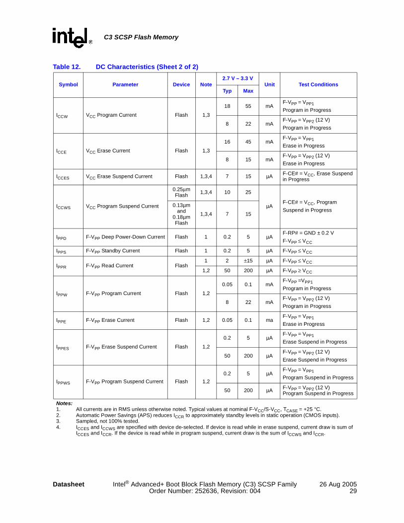
C3 SCSP Flash Memory
Datasheet Intel® Advanced+ Boot Block Flash Memory (C3) SCSP Family 26 Aug 2005Order Number: 252636, Revision: 004 29
ICCW VCC Program Current Flash 1,3
18 55 mAF-VPP = VPP1
Program in Progress
8 22 mAF-VPP = VPP2 (12 V)
Program in Progress
ICCE VCC Erase Current Flash 1,3
16 45 mAF-VPP = VPP1
Erase in Progress
8 15 mAF-VPP = VPP2 (12 V)
Erase in Progress
ICCES VCC Erase Suspend Current Flash 1,3,4 7 15 µA F-CE# = VCC, Erase Suspend in Progress
ICCWS VCC Program Suspend Current
0.25µm Flash 1,3,4 10 25
µAF-CE# = VCC, Program
Suspend in Progress0.13µm
and 0.18µm Flash
1,3,4 7 15
IPPD F-VPP Deep Power-Down Current Flash 1 0.2 5 µAF-RP# = GND ± 0.2 V
F-VPP ≤ VCC
IPPS F-VPP Standby Current Flash 1 0.2 5 µA F-VPP ≤ VCC
IPPR F-VPP Read Current Flash1 2 ±15 µA F-VPP ≤ VCC
1,2 50 200 µA F-VPP ≥ VCC
IPPW F-VPP Program Current Flash 1,2
0.05 0.1 mAF-VPP =VPP1
Program in Progress
8 22 mAF-VPP = VPP2 (12 V)
Program in Progress
IPPE F-VPP Erase Current Flash 1,2 0.05 0.1 maF-VPP = VPP1
Erase in Progress
IPPES F-VPP Erase Suspend Current Flash 1,2
0.2 5 µAF-VPP = VPP1
Erase Suspend in Progress
50 200 µAF-VPP = VPP2 (12 V)
Erase Suspend in Progress
IPPWS F-VPP Program Suspend Current Flash 1,2
0.2 5 µAF-VPP = VPP1
Program Suspend in Progress
50 200 µA F-VPP = VPP2 (12 V)Program Suspend in Progress
Notes:1. All currents are in RMS unless otherwise noted. Typical values at nominal F-VCC/S-VCC, TCASE = +25 °C.2. Automatic Power Savings (APS) reduces ICCR to approximately standby levels in static operation (CMOS inputs).3. Sampled, not 100% tested.4. ICCES and ICCWS are specified with device de-selected. If device is read while in erase suspend, current draw is sum of
ICCES and ICCR. If the device is read while in program suspend, current draw is the sum of ICCWS and ICCR.
Table 12. DC Characteristics (Sheet 2 of 2)
Symbol Parameter Device Note2.7 V – 3.3 V
Unit Test ConditionsTyp Max

C3 SCSP Flash Memory
26 Aug 2005 Intel® Advanced+ Boot Block Flash Memory (C3) SCSP Family Datasheet30 Order Number: 252636, Revision: 004
Note: CL includes jig capacitance.
Table 13. DC Characteristics
Symbol Parameter Device Note2.7 V – 3.3 V
Units Test ConditionsMin Max
VIL Input Low Voltage Flash/SRAM –0.2 0.6 V
VIH Input High Voltage Flash/SRAM 2.3 VCC
+0.2 V
VOL Output Low Voltage Flash/SRAM –0.10 0.10 V
F-VCC/S-VCC = VCC Min
IOL = 100 µA
VOH Output High Voltage Flash/SRAM
VCC –0.1 V
F-VCC/S-VCC = VCC Min
IOH = –100 µA
VPPLK F-VPP Lock-Out Voltage Flash 1 1.0 V Complete Write Protection
VPP1 F-VPP during Program / Erase Flash 1 1.65 3.3 V
VPP2 Operations 1,2 11.4 12.6
VLKO VCC Prog/Erase Lock Voltage Flash 1.5 V
VLKO2 VCCQ Prog/Erase Lock Voltage Flash 1.2 V
Notes:1. Erase and Program are inhibited when F-Vpp < VPPLK and not guaranteed outside the valid F-Vpp ranges of VPP1 and
VPP2.2. Applying F-Vpp = 11.4V–12.6V during program/erase can only be done for a maximum of 1000 cycles on the main
blocks and 2500 cycles on the parameter blocks. F-Vpp may be connected to 12 V for a total of 80 hours maximum. See Section 4.2.1 for details.
Figure 4. Input/Output Reference Waveform
Note: AC test inputs are driven at VCCQ for a logic “1” and 0.0V for a logic “0.” Input timing begins, and output timing ends, at VCCQ/2. Input rise and fall times (10%–90%) <10 ns. Worst case speed conditions are when VCCQ = VCCQMin.
Figure 5. Test Configuration
INPUT OUTPUTTEST POINTS
VCC
0.0
VCC
2VCC
2
DeviceUnder Test Out
CL

C3 SCSP Flash Memory
Datasheet Intel® Advanced+ Boot Block Flash Memory (C3) SCSP Family 26 Aug 2005Order Number: 252636, Revision: 004 31
Flash Test Configuration Component Values Table
Test Configuration CL (pF)
2.7 V–3.3 V Standard Test 50
C3 SCSP Flash Memory
26 Aug 2005 Intel® Advanced+ Boot Block Flash Memory (C3) SCSP Family Datasheet32 Order Number: 252636, Revision: 004
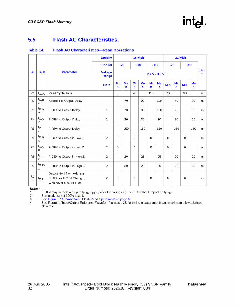
5.5 Flash AC Characteristics.
Table 14. Flash AC Characteristics—Read Operations
# Sym Parameter
Density 16-Mbit 32-Mbit
Unit
Product -70 -90 -110 -70 -90
VoltageRange 2.7 V - 3.3 V
Note Min
Max
Min
Max
Min
Max Min Ma
x Min Max
R1 tAVAV Read Cycle Time 70 90 110 70 90 ns
R2 tAVQV
Address to Output Delay 70 90 110 70 90 ns
R3 tELQV
F-CE# to Output Delay 1 70 90 110 70 90 ns
R4 tGLQV
F-OE# to Output Delay 1 20 30 30 20 20 ns
R5 tPHQV
F-RP# to Output Delay 150 150 150 150 150 ns
R6 tELQX
F-CE# to Output in Low Z 2 0 0 0 0 0 ns
R7 tGLQX
F-OE# to Output in Low Z 2 0 0 0 0 0 ns
R8 tEHQZ
F-CE# to Output in High Z 2 20 25 25 20 20 ns
R9 tGHQZ
F-OE# to Output in High Z 2 20 20 20 20 20 ns
R10 tOH
Output Hold from Address
F-CE#, or F-OE# Change,
Whichever Occurs First
2 0 0 0 0 0 ns
Notes:1. F-OE# may be delayed up to tELQV–tGLQV after the falling edge of CE# without impact on tELQV2. Sampled, but not 100% tested.3. See Figure 6 “AC Waveform: Flash Read Operations” on page 33.4. See Figure 4, “Input/Output Reference Waveform” on page 28 for timing measurements and maximum allowable input
slew rate.
C3 SCSP Flash Memory
Datasheet Intel® Advanced+ Boot Block Flash Memory (C3) SCSP Family 26 Aug 2005Order Number: 252636, Revision: 004 33
5.6 Flash AC Characteristics—Write Operations
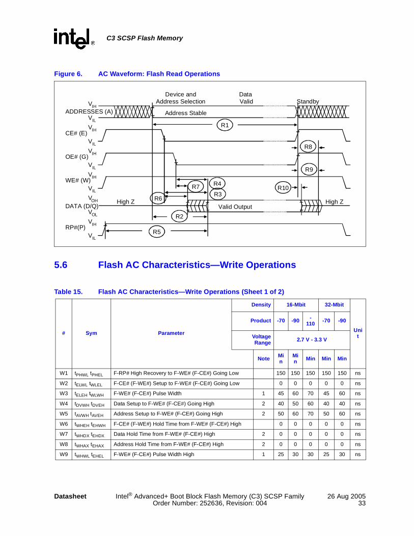
Figure 6. AC Waveform: Flash Read Operations
Table 15. Flash AC Characteristics—Write Operations (Sheet 1 of 2)
# Sym Parameter
Density 16-Mbit 32-Mbit
Unit
Product -70 -90 -110 -70 -90
VoltageRange 2.7 V - 3.3 V
Note Min
Min Min Min Min
W1 tPHWL tPHEL F-RP# High Recovery to F-WE# (F-CE#) Going Low 150 150 150 150 150 ns
W2 tELWL tWLEL F-CE# (F-WE#) Setup to F-WE# (F-CE#) Going Low 0 0 0 0 0 ns
W3 tELEH tWLWH F-WE# (F-CE#) Pulse Width 1 45 60 70 45 60 ns
W4 tDVWH tDVEH Data Setup to F-WE# (F-CE#) Going High 2 40 50 60 40 40 ns
W5 tAVWH tAVEH Address Setup to F-WE# (F-CE#) Going High 2 50 60 70 50 60 ns
W6 tWHEH tEHWH F-CE# (F-WE#) Hold Time from F-WE# (F-CE#) High 0 0 0 0 0 ns
W7 tWHDX tEHDX Data Hold Time from F-WE# (F-CE#) High 2 0 0 0 0 0 ns
W8 tWHAX tEHAX Address Hold Time from F-WE# (F-CE#) High 2 0 0 0 0 0 ns
W9 tWHWL tEHEL F-WE# (F-CE#) Pulse Width High 1 25 30 30 25 30 ns
Address Stable
Device andAddress Selection
IHV
ILVADDRESSES (A)
IHV
ILV
IHV
ILV
IHV
ILV
CE# (E)
OE# (G)
WE# (W)
DATA (D/Q)
IHV
ILVRP#(P)
OLV
OHVHigh Z
Valid Output
DataValid Standby
High Z
R1
R2
R3
R4
R5
R6
R7
R8
R9
R10

C3 SCSP Flash Memory
26 Aug 2005 Intel® Advanced+ Boot Block Flash Memory (C3) SCSP Family Datasheet34 Order Number: 252636, Revision: 004
See Figure 4 “Input/Output Reference Waveform” on page 30 for timing measurements and maximum allowable input slew rate.
See Figure 7 “AC Waveform: Flash Program and Erase Operations” on page 35.
5.7 Flash Erase and Program Timings(1)
W10 tVPWH tVPEH F-VPP Setup to F-WE# (F-CE#) Going High 3 200 200 200 200 200 ns
W11 tQVVL F-VPP Hold from Valid SRD 3 0 0 0 0 0 ns
Notes:1. Write pulse width (tWP) is defined from F-CE# or F-WE# going low (whichever goes low last) to F-CE# or
F-WE# going high (whichever goes high first). Hence, tWP= tWLWH = tELEH = tWLEH = tELWH. Similarly, write pulse width high (tWPH) is defined from F-CE# or F-WE# going high (whichever goes high first) to F-CE# or F-WE# going low (whichever goes low first). Hence, tWPH = tWHWL = tEHEL = tWHEL = tEHWL.
2. Refer to Table 5 “Flash Memory Command Definitions” on page 19 for valid AIN or DIN.3. Sampled, but not 100% tested.
Table 15. Flash AC Characteristics—Write Operations (Sheet 2 of 2)
# Sym Parameter
Density 16-Mbit 32-Mbit
Unit
Product -70 -90 -110 -70 -90
VoltageRange 2.7 V - 3.3 V
Note Min
Min Min Min Min
Table 16. Flash Erase and Program Timings
Symbol ParameterF-VPP 1.65 V– 3.3 V 11.4 V– 12.6 V
UnitNote Typ(1) Max Typ(1) Max
tBWPB 4-KW Parameter Block Program Time (Word) 2, 3 0.10 0.30 0.03 0.12 s
tBWMB 32-KW Main Block Program Time (Word) 2, 3 0.8 2.4 0.24 1 s
tWHQV1 / tEHQV1
0.25 µm Word Program Time 2, 3 22 200 8 185µs
0.13 µm and 0.18 µm Word Program Time 2, 3 12 200 8 185
tWHQV2 / tEHQV2 4-KW Parameter Block Erase Time (Word) 2, 3 0.5 4 0.4 4 s
tWHQV3 / tEHQV3 32-KW Main Block Erase Time (Word) 2, 3 1 5 0.6 5 s
tWHRH1 / tEHRH1 Program Suspend Latency 3 5 10 5 10 µs
tWHRH2 / tEHRH2 Erase Suspend Latency 3 5 20 5 20 µs
Notes:1. Typical values measured at TCASE = +25 °C and nominal voltages.2. Excludes external system-level overhead.3. Sampled, but not 100% tested.

C3 SCSP Flash Memory
Datasheet Intel® Advanced+ Boot Block Flash Memory (C3) SCSP Family 26 Aug 2005Order Number: 252636, Revision: 004 35
Notes:1. F-CE# must be toggled low when reading Status Register Data. F-WE# must be inactive (high) when
reading Status Register Data.2. F-VCC Power-Up and Standby.3. Write Program or Erase Setup Command.4. Write Valid Address and Data (for Program) or Erase Confirm Command.5. Automated Program or Erase Delay.6. Read Status Register Data (SRD): reflects completed program/erase operation.7. Write Read Array Command.
Figure 7. AC Waveform: Flash Program and Erase Operations
ADDRESSES [A]
CE#(WE#) [E(W)]
OE# [G]
WE#(CE#) [W(E)]
DATA [D/Q]
RP# [P]
IHV
ILV
IHV
ILV
IHV
ILV
IHV
ILV
ILV
ILV
IND
INA INA
ValidSRDIND
IHV
High Z
IHV
ILV
V [V]PP
PPHV
PPLKVPPHV 1
2
WP# ILV
IHV
IND
A B C D E F
W8
W6
W9
W3
W4
W7
W1
W5
W2
W10 W11
(Note 1)
(Note 1)
ADDRESSES [A]
CE#(WE#) [E(W)]
OE# [G]
WE#(CE#) [W(E)]
DATA [D/Q]
RP# [P]
IHV
ILV
IHV
ILV
IHV
ILV
IHV
ILV
ILV
ILV
IND
INA INA
ValidSRDIND
IHV
High Z
IHV
ILV
V [V]PP
PPHV
PPLKVPPHV 1
2
WP# ILV
IHV
IND
A B C D E F
W8
W6
W9
W3
W4
W7
W1
W5
W2
W10 W11
(Note 1)
(Note 1)

C3 SCSP Flash Memory
26 Aug 2005 Intel® Advanced+ Boot Block Flash Memory (C3) SCSP Family Datasheet36 Order Number: 252636, Revision: 004
5.8 Flash Reset Operations
Figure 8. AC Waveform: Reset Operation
Table 17. Reset Specifications(1)
Symbol Parameter NoteF-VCC 2.7 V – 3.3 V
UnitMin Max
tPLPHF-RP# Low to Reset during Read (If F-RP# is tied to VCC, this specification is not applicable) 2,4 100 ns
tPLRH1 F-RP# Low to Reset during Block Erase 3,4 22 µs
tPLRH2 F-RP# Low to Reset during Program 3,4 12 µs
Notes:1. See Section 2.1.4, “Flash Reset” on page 13 for a full description of these conditions.2. If tPLPH is < 100 ns the device may still reset but this is not guaranteed.3. If F-RP# is asserted while a block erase or word program operation is not executing, the reset will
complete within 100 ns.4. Sampled, but not 100% tested.
IHV
ILV
RP# (P)
PLPHt
IHV
ILVRP# (P)
PLPHt(A) Reset during Read Mode
AbortComplete PHQVt
PHWLtPHELt
PHQVtPHWLtPHELt
(B) Reset during Program or Block Erase, <PLPHt PLRHt
PLRHt
IHV
ILV
RP# (P)
PLPHt
AbortComplete PHQVt
PHWLtPHELtPLRHt
DeepPower-Down
(C) Reset Program or Block Erase, > PLPHt PLRHt

C3 SCSP Flash Memory
Datasheet Intel® Advanced+ Boot Block Flash Memory (C3) SCSP Family 26 Aug 2005Order Number: 252636, Revision: 004 37
5.9 SRAM AC Characteristics—Read Operations
Table 18. SRAM AC Characteristics—Read Operations(1)
# Sym Parameter
Density 2/4/8-Mbit
UnitVoltage Range 2.7 V– 3.3 V
Note Min Max
R1 tRC Read Cycle Time 70 – ns
R2 tAA Address to Output Delay – 70 ns
R3 tCO1, tCO2 S-CS1#, S-CS2 to Output Delay – 70 ns
R4 tOE S-OE# to Output Delay – 35 ns
R5 tBA S-UB#, LB# to Output Delay – 70 ns
R6 tLZ1, tLZ2 S-CS1#, S-CS2 to Output in Low Z 2,3 5 – ns
R7 tOLZ S-OE# to Output in Low Z 3 0 – ns
R8 tHZ1, tHZ2 S-CS1#, S-CS2 to Output in High Z 2,3,4 0 25 ns
R9 tOHZ S-OE# to Output in High Z 3,4 0 25 ns
R10 tOH
Output Hold from Address, S-CS1#, S-CS2, or S-OE# Change, Whichever Occurs First
0 – ns
R11 tBLZ S-UB#, S-LB# to Output in Low Z 3 0 – ns
R12 tBHZ S-UB#, S-LB# to Output in High Z 3 0 25 ns
Note:1. See Figure 9 “AC Waveform: SRAM Read Operations” on page 38.2. At any given temperature and voltage condition, tHZ (Max) is less than and tLZ (Max) both for a given
device and from device to device interconnection.3. Sampled, but not 100% tested.4. Timings of tHZ and tOHZ are defined as the time at which the outputs achieve the open circuit
conditions and are not referenced to output voltage levels.
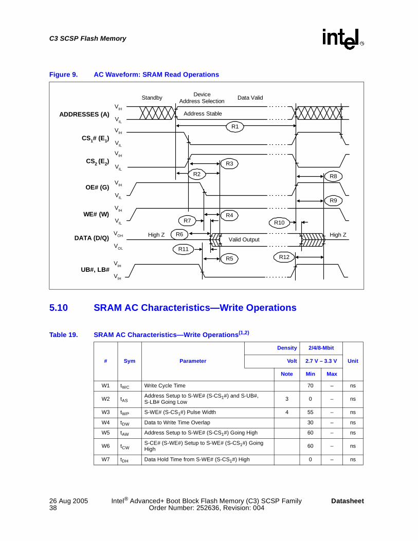
C3 SCSP Flash Memory
26 Aug 2005 Intel® Advanced+ Boot Block Flash Memory (C3) SCSP Family Datasheet38 Order Number: 252636, Revision: 004
5.10 SRAM AC Characteristics—Write Operations
Figure 9. AC Waveform: SRAM Read Operations
Table 19. SRAM AC Characteristics—Write Operations(1,2)
# Sym Parameter
Density 2/4/8-Mbit
UnitVolt 2.7 V – 3.3 V
Note Min Max
W1 tWC Write Cycle Time 70 – ns
W2 tASAddress Setup to S-WE# (S-CS1#) and S-UB#, S-LB# Going Low 3 0 – ns
W3 tWP S-WE# (S-CS1#) Pulse Width 4 55 – ns
W4 tDW Data to Write Time Overlap 30 – ns
W5 tAW Address Setup to S-WE# (S-CS1#) Going High 60 – ns
W6 tCWS-CE# (S-WE#) Setup to S-WE# (S-CS1#) Going High 60 – ns
W7 tDH Data Hold Time from S-WE# (S-CS1#) High 0 – ns
High ZValid Output
Address Stable
Data ValidDevice
Address SelectionStandby
ADDRESSES (A)VIH
VIL
VIH
VIL
CS1# (E1)
VIH
VIL
VOH
VOL
VIH
OE# (G)
WE# (W)
DATA (D/Q)
UB#, LB#
High Z
VIH
VIL
R1
R2
R4
R3
R6
R7
R8
R9
R10
CS2 (E2)VIH
VIL
VIH
R5
R11R12

C3 SCSP Flash Memory
Datasheet Intel® Advanced+ Boot Block Flash Memory (C3) SCSP Family 26 Aug 2005Order Number: 252636, Revision: 004 39
W8 tWR Write Recovery 5 0 – ns
W9 tBW S-UB#, S-LB# Setup to S-WE# (S-CS1#) Going High 60 – ns
Notes:1. See Figure 10 “AC Waveform: SRAM Write Operations” on page 39.2. A write occurs during the overlap (tWP) of low S-CS1# and low S-WE#. A write begins when S-CS1#
goes low and S-WE# goes low with asserting S-UB# or S-LB# for single byte operation or simultaneously asserting S-UB# and S-LB# for double byte operation. A write ends at the earliest transition when S-CS1# goes high and S-WE# goes high. The tWP is measured from the beginning of write to the end of write.
3. tAS is measured from the address valid to the beginning of write.4. tWP is measured from S-CS1# going low to end of write.5. tWR is measured from the end of write to the address change. tWR applied in case a write ends as S-
CS1# or S-WE# going high.
Figure 10. AC Waveform: SRAM Write Operations
Table 19. SRAM AC Characteristics—Write Operations(1,2)
# Sym Parameter
Density 2/4/8-Mbit
UnitVolt 2.7 V – 3.3 V
Note Min Max
High ZData In
Address Stable
DeviceAddress Selection
Standby
ADDRESSES (A)VIH
VIL
VIH
VIL
CS1# (E1)
VIH
VIL
VOH
VOL
VIH
OE# (G)
WE# (W)
DATA (D/Q)
UB#, LB#
High Z
VIH
VIL
W1
W8
CS2 (E2)VIH
VIL
VIH
W9
W6
W5
W2
W3
W4W7

C3 SCSP Flash Memory
26 Aug 2005 Intel® Advanced+ Boot Block Flash Memory (C3) SCSP Family Datasheet40 Order Number: 252636, Revision: 004
5.11 SRAM Data Retention Characteristics—Extended Temperature
Table 20. SRAM Data Retention Characteristics(1)—Extended Temperature
Sym Parameter Note Min Typ Max Unit Test Conditions
VDR S-VCC for Data Retention
2
1.5 – 3.3 V CS1# ≥VCC – 0.2 V
IDR
Deep Retention Current -
8-Mbit– – 6 µA
S-VCC = 1.5 VCS1# ≥VCC – 0.2 V
Deep Retention Current -
4-Mbit– – 5 µA
Deep Retention Current -
2-Mbit– – 4 µA
tSDR Data Retention Set-up Time 0 – – ns See Data Retention Waveform
tRDR Recovery Time tRC – – ns
Notes:1. Typical values at nominal S-VCC, TCASE = +25 °C.2. S-CS1# ≥ VCC – 0.2 V, S-CS2 ≥ VCC – 0.2 V (S-CS1# controlled) or S-CS2 ≤ 0.2 V (S-CS2 controlled).
Figure 11. SRAM Data Retention Waveform
VCC
3.0/2.7V
CS1# (E1) 2.2V
VDR
CS2 (E2)
GND
VCC
3.0/2.7V
0.4V
VDR
GND
CS1# Controlled
CS2 Controlled
Data Retention ModetSDR tRDR
Data Retention ModetSDR tRDR

C3 SCSP Flash Memory
Datasheet Intel® Advanced+ Boot Block Flash Memory (C3) SCSP Family 26 Aug 2005Order Number: 252636, Revision: 004 41
6.0 Migration Guide Information
Typically, it is important to discuss footprint migration compatibility between a new product and existing products. In this specific case, the SCSP allows the system designer to remove two separate memory footprints for individual flash and SRAM and replace them with a single footprint, thus resulting in an overall reduction in board space required. This implies that a new printed circuit board would be used to take advantage of this feature.
Since the flash in SCSP shares the same features as the C3 features, conversions from the C3 are described in AP-658 Designing for Upgrade to the Advanced+ Boot Block Flash Memory, order number 292216.
Please contact your local Intel representation for detailed information about specific Flash + SRAM system migrations.
7.0 System Design Considerations
This section contains information that would have been contained in a product design guide in earlier generations. In an effort to simplify the amount of documentation, relevant system design considerations have been combined into this document.
7.1 Background
The C3 SCSP combines the features of the C3 flash memory architecture with a low-power SRAM to achieve an overall reduction in system board space. This enables applications to integrate security with simple software and hardware configurations, while also combining the system SRAM and flash into one common footprint. This section discusses how to take full advantage of the C3 SCSP.
7.1.1 Flash + SRAM Footprint Integration
The SCSP memory solution can be used to replace a subset of the memory subsystem within a design. Where a previous design may have used two separate footprints for SRAM and Flash, you can now replace with the industry-standard I-ballout of the SCSP device. This allows for an overall reduction in board space, which allows the design to integrate both the flash and the SRAM into one component.
C3 SCSP Flash Memory
26 Aug 2005 Intel® Advanced+ Boot Block Flash Memory (C3) SCSP Family Datasheet42 Order Number: 252636, Revision: 004
7.1.2 C3 Flash Memory Features
C3 adds the following new features to Intel Advanced Boot Block architecture:
• Instant, individual block locking provides software/hardware controlled, independent locking/unlocking of any block with zero latency to protect code and data.
• A 128-bit Protection Register enables system security implementations.
• Improved 12 V production programming simplifies the system configuration required to implement 12 V fast programming.
• Common Flash Interface (CFI) provides component information on the chip to allow software-independent device upgrades.
For more information on specific advantages of the C3, please see AP-658 Designing with the Advanced+ Boot Block Flash Memory Architecture.
7.2 Flash Control Considerations
The flash device is protected against accidental block erasure or programming during power transitions. Power supply sequencing is not required, since the device is indifferent as to which power supply, F-VPP or F-VCC, powers-up first. Example flash power supply configurations are shown in Figure 12 “Example Power Supply Configurations” on page 43.
7.2.1 F-RP# Connected to System Reset
The use of F-RP# during system reset is important with automated program/erase devices since the system expects to read from the flash memory when it comes out of reset. If a CPU reset occurs without a flash memory reset, proper CPU initialization will not occur because the flash memory may be providing status information instead of array data. Intel recommends connecting F-RP# to the system CPU RESET# signal to allow proper CPU/flash initialization following system reset.
System designers must guard against spurious writes when F-VCC voltages are above VLKO. Since both F-WE# and F-CE# must be low for a command write, driving either signal to VIH will inhibit writes to the device. The CUI architecture provides additional protection since alteration of memory contents can only occur after successful completion of the two-step command sequences. The device is also disabled until F-RP# is brought to VIH, regardless of the state of its control inputs.
By holding the device in reset (F-RP# connected to system PowerGood) during power-up/down, invalid bus conditions during power-up can be masked, providing yet another level of memory protection.
7.2.2 F-VCC, F-VPP and F-RP# Transition
The CUI latches commands as issued by system software and is not altered by F-VPP or F-CE# transitions or WSM actions. Its default state upon power-up, after exit from reset mode or after F-VCC transitions above VLKO (Lockout voltage), is read array mode.
After any program or block erase operation is complete (even after F-VPP transitions down to VPPLK), the CUI must be reset to read array mode via the Read Array command if access to the flash memory array is desired.

C3 SCSP Flash Memory
Datasheet Intel® Advanced+ Boot Block Flash Memory (C3) SCSP Family 26 Aug 2005Order Number: 252636, Revision: 004 43
Note: 1. A resistor can be used if the F-VCC supply can sink adequate current based on resistor value.
7.3 Noise Reduction
SCSP memory’s power switching characteristics require careful device decoupling. System designers should consider three supply current issues for both the flash and SRAM:
• Standby current levels (ICCS)
• Read current levels (ICCR)
• Transient peaks produced by falling and rising edges of F-CE#, S-CS1#, and S-CS2.
Transient current magnitudes depend on the device outputs’ capacitive and inductive loading. Two-line control and proper decoupling capacitor selection will suppress these transient voltage peaks. Each device should have a capacitors between individual power (F-VCC, F-VCCQ, F-VPP, S-VCC) and ground (GND) signals. High-frequency, inherently low-inductance capacitors should be placed as close as possible to the package leads.
Noise issues within a system can cause devices to operate erratically if it is not adequately filtered. In order to avoid any noise interaction issues within a system, it is recommended that the design contain the appropriate number of decoupling capacitors in the system. Noise issues can also be reduced if leads to the device are kept very short, in order to reduce inductance.
Decoupling capacitors between VCC and VSS reduce voltage spikes by supplying the extra current needed during switching. Placing these capacitors as close to the device as possible reduces line inductance. The capacitors should be low inductance capacitors; surface mount capacitors typically exhibit lower inductance.
It is highly recommended that systems use a 0.1 µf capacitor for each of the D9, D10, A10 and E4 grid ballout locations (see Figure 1 “66-Ball SCSP Package Ballout” on page 8 for ballout). These capacitors are necessary to avoid undesired conditions created by excess noise. Smaller capacitors can be used to decouple higher frequencies.
Figure 12. Example Power Supply Configurations
VCC
VPP
12 V Fast Programming
Absolute Write Protection With V PP ≤ VPPLK
System Supply
12 V Supply
10 ≤ KΩ
VCC
VPP
System Supply
12 V Supply
Low Voltage and 12 V Fast Programming
VCC
VPP
System Supply
Prot#(Logic Signal)
VCC
VPP
System Supply
Low-Voltage Programming
Low-Voltage Programming
Absolute Write Protection via Logic Signal
(Note 1)

C3 SCSP Flash Memory
26 Aug 2005 Intel® Advanced+ Boot Block Flash Memory (C3) SCSP Family Datasheet44 Order Number: 252636, Revision: 004
Notes:1. Substrate connections refer to ballout locations shown in Figure 1 “66-Ball SCSP Package Ballout” on
page 8.2. 0.1µf capacitors should be used with D9, D10, A10and E4.3. Some SRAM devices do not have a S-VSSQ; in this case, this pad is a S-VSS.4. Some SRAM devices do not have a S-VSSQ; in this case, this pad is a VCC.
7.4 Simultaneous Operation
The term simultaneous operation in used to describe the ability to read or write to the SRAM while also programming or erasing flash. In addition, F-CE#, S-CS1# and S-CS2 should not be enabled at the same time. (See Table 2 “Intel® Advanced+ Boot Block SCSP Ball Descriptions” on page 9 for a summary of recommended operating modes.) Simultaneous operation of the can be summarized by the following:
• SRAM read/write are during a Flash Program or Erase Operation are allowed.
• Simultaneous Bus Operations between the Flash and SRAM are not allowed (because of bus contention).
Figure 13. Typical Flash + SRAM Substrate Power and Ground Connections
S-VSSQ
D10
SRAM DIEFLASH DIE
SUBSTRATE
XX
S-X
F-X
Substrate connection to package ball
SRAM die bond pad connection
Flash die bond pad connection
S-VCCQ
S-VCCS-VSS
F-VPP
F-VSSQ
F-VCC
F-VCCQ
F-VSS H8
A9
D9
E4
D3
A10

C3 SCSP Flash Memory
Datasheet Intel® Advanced+ Boot Block Flash Memory (C3) SCSP Family 26 Aug 2005Order Number: 252636, Revision: 004 45
7.4.1 SRAM Operation during Flash “Busy”
This functionality provides the ability to use both the flash and the SRAM “at the same time” within a system, similar to the operation of two devices with separate footprints. This operation can be achieved by following the appropriate timing constraints within a system.
7.4.2 Simultaneous Bus Operations
Operations that require both the SRAM and Flash to be in active mode are disallowed. An example of these cases would include simultaneous reads on both the flash and SRAM, which would result in contention for the data bus. Finally, a read of one device while attempting to write to the other (similar to the conditions of direct memory access (DMA) operation) are also not within the recommended operating conditions. Basically, only one memory can drive the outputs out the device at one given point in time.
7.5 Printed Circuit Board Notes
The Intel SCSP will save significant space on your PCB by combining two chips into one BGA style package. Intel SCSP has a 0.8 mm pitch that can be routed on your Printed Circuit Board with conventional design rules. Trace widths of 0.127 mm (0.005 inches) are typical. Unused balls in the center of the package are not populated to further increase the routing options. Standard surface mount process and equipment can be used for the Intel SCSP.
Note: Top View
7.6 System Design Notes Summary
The C3 SCSP allows higher levels of memory component integration. Different power supply configurations can be used within the system to achieve different objectives. At least three different 0.1 µf capacitors should be used to decouple the devices within a system. SRAM reads or writes during a flash program or erase are supported operations. Standard printed circuit board technology can be used.
Figure 14. Standard PCB Design Rules Can be Used with SCSP Device
Land Pad Diameter: 0.35 mm (0.0138 in)Solder Mask Opening: 0.50 mm (0.0198 in)
Trace Width: 0.127 mm (0.005 in)Trace Spaces: 0.160 mm (0.00625 in)
Via Capture Pad: 0.51 mm (0.020 in)Via Drill Size: 0.25 mm (0.010 in)

C3 SCSP Flash Memory
26 Aug 2005 Intel® Advanced+ Boot Block Flash Memory (C3) SCSP Family Datasheet46 Order Number: 252636, Revision: 004
Appendix A Program/Erase Flowcharts
Figure 15. Automated Word Programming Flowchart
Start
Write 40H
Program Address/Data
Read Status Register
SR.7 = 1?
Full StatusCheck if Desired
Program Complete
Read Status RegisterData (See Above)
VPP Range Error
Programming Error
Attempted Program toLocked Block - Aborted
Program Successful
SR.3 =
SR.4 =
SR.1 =
FULL STATUS CHECK PROCEDURE
Bus Operation
Write
Write
Standby
Repeat for subsequent programming operations.
SR Full Status Check can be done after each program or after a sequence ofprogram operations.
Write FFH after the last program operation to reset device to read array mode.
Bus Operation
Standby
Standby
SR.3 MUST be cleared, if set during a program attempt, before furtherattempts are allowed by the Write State Machine.
SR.1, SR.3 and SR.4 are only cleared by the Clear Staus Register Command,in cases where multiple bytes are programmed before full status is checked.
If an error is detected, clear the status register before attempting retry or othererror recovery.
No
Yes
1
0
10
1
0
Command
Program Setup
Program
Comments
Data = 40H
Data = Data to ProgramAddr = Location to Program
Check SR.71 = WSM Ready0 = WSM Busy
Command Comments
Check SR.31 = VPP Low Detect
Check SR.11 = Attempted Program toLocked Block - ProgramAborted
ReadStatus Register Data ToggleCE# or OE# to Update StatusRegister Data
StandbyCheck SR.41 = VPP Program Error

C3 SCSP Flash Memory
Datasheet Intel® Advanced+ Boot Block Flash Memory (C3) SCSP Family 26 Aug 2005Order Number: 252636, Revision: 004 47
0645_13
Figure 16. Program Suspend/Resume Flowchart
Start
Write B0H
Read Status Register
No
Comments
Data = B0HAddr = X
Data = FFHAddr = X
SR.7 =
SR.2 =
1
Write FFH
Read Array Data
Program Completed
DoneReading
Yes
Write FFHWrite D0H
Program Resumed Read Array Data
0
1
Read array data from blockother than the one beingprogrammed.
Status Register Data ToggleCE# or OE# to Update StatusRegister DataAddr = X
Check SR.71 = WSM Ready0 = WSM Busy
Check SR.21 = Program Suspended0 = Program Completed
Data = D0HAddr = X
BusOperation Command
0
Write 70HStatus Register Data ToggleCE# or OE# to Update StatusRegister DataAddr = X
Write
Write
Write
Read
Read
Standby
Standby
Write
Data = 70HAddr = X
Command
ProgramSuspend
Read Status
Read Array
ProgramResume

C3 SCSP Flash Memory
26 Aug 2005 Intel® Advanced+ Boot Block Flash Memory (C3) SCSP Family Datasheet48 Order Number: 252636, Revision: 004
0645_14
Figure 17. Automated Block Erase Flowchart
Start
Write 20H
Write D0H andBlock Address
Read Status Register
SR.7 =
Full StatusCheck if Desired
Block Erase Complete
FULL STATUS CHECK PROCEDURE
Bus Operation
Write
Write
Standby
Repeat for subsequent block erasures.
Full Status Check can be done after each block erase or after a sequence ofblock erasures.
Write FFH after the last write operation to reset device to read array mode.
Bus Operation
Standby
SR. 1 and 3 MUST be cleared, if set during an erase attempt, before furtherattempts are allowed by the Write State Machine.
SR.1, 3, 4, 5 are only cleared by the Clear Staus Register Command, in caseswhere multiple bytes are erased before full status is checked.
If an error is detected, clear the status register before attempting retry or othererror recovery.
NoYes
Suspend Erase
SuspendErase Loop
1
0
Standby
Command
Erase Setup
Erase Confirm
Comments
Data = 20HAddr = Within Block to BeErased
Data = D0HAddr = Within Block to BeErased
Check SR.71 = WSM Ready0 = WSM Busy
Command Comments
Check SR.31 = VPP Low Detect
Check SR.4,5Both 1 = Command SequenceError
Read Status RegisterData (See Above)
VPP Range Error
Command SequenceError
Block EraseSuccessful
SR.3 =
SR.4,5 =
1
0
10
Block Erase ErrorSR.5 =1
0
Attempted Erase ofLocked Block - Aborted
SR.1 =1
0
ReadStatus Register Data ToggleCE# or OE# to Update StatusRegister Data
StandbyCheck SR.51 = Block Erase Error
StandbyCheck SR.11 = Attempted Erase ofLocked Block - Erase Aborted

C3 SCSP Flash Memory
Datasheet Intel® Advanced+ Boot Block Flash Memory (C3) SCSP Family 26 Aug 2005Order Number: 252636, Revision: 004 49
0645_15
Figure 18. Erase Suspend/Resume Flowchart
Start
Write B0H
Read Status Register
No
Comments
Data = B0HAddr = X
Data = FFHAddr = X
SR.7 =
SR.6 =
1
Write FFH
Read Array Data
Erase Completed
DoneReading
Yes
Write FFHWrite D0H
Erase Resumed Read Array Data
0
1
Read array data from blockother than the one beingerased.
Status Register Data ToggleCE# or OE# to Update StatusRegister DataAddr = X
Check SR.71 = WSM Ready0 = WSM Busy
Check SR.61 = Erase Suspended0 = Erase Completed
Data = D0HAddr = X
BusOperation
Write
Standby
Write
Read
Standby
Read
Command
0
Write 70HStatus Register Data ToggleCE# or OE# to Update StatusRegister DataAddr = X
Write
Write
Data = 70HAddr = X
Command
Erase Suspend
Read Status
Read Array
Erase Resume

C3 SCSP Flash Memory
26 Aug 2005 Intel® Advanced+ Boot Block Flash Memory (C3) SCSP Family Datasheet50 Order Number: 252636, Revision: 004
0645_16
Figure 19. Locking Operations Flowchart
Start
Write 60H(Configuration Setup)
No
Comments
Data = 60HAddr = X
Write 90H(Read Configuration)
Read Block Lock Status
LockingChange
Confirmed?
Locking ChangeComplete
BusOperation
Write
Command
Write01H, D0H, or 2FH
Write
Write
Data= 01H (Lock Block) D0H (Unlock Block) 2FH (Lockdown Block)Addr=Within block to lock
Command
Config. Setup
Lock, Unlock,or Lockdown
Data = 90HAddr = X
Write(Optional)
ReadConfiguration
Block Lock Status DataAddr = Second addr of block
Read(Optional)
Block LockStatus
Confirm Locking Change onDQ1, DQ0. (See Block LockingState Table for validcombinations.)
Standby(Optional)
Opt
iona
l
Write FFh(Read Array)

C3 SCSP Flash Memory
Datasheet Intel® Advanced+ Boot Block Flash Memory (C3) SCSP Family 26 Aug 2005Order Number: 252636, Revision: 004 51
0645_17
Figure 20. Protection Register Programming Flowchart
Start
Write C0H(Protection Reg.Program Setup)
Write Protect. RegisterAddress/Data
Read Status Register
SR.7 = 1?
Full StatusCheck if Desired
Program Complete
Read Status RegisterData (See Above)
VPP Range Error
Protection RegisterProgramming Error
Attempted Program toLocked Register -
Aborted
Program Successful
SR.3, SR.4 =
SR.1, SR.4 =
SR.1, SR.4 =
FULL STATUS CHECK PROCEDURE
Bus Operation
Write
Write
Standby
Protection Program operations can only be addressed within the protectionregister address space. Addresses outside the defined space will return anerror.
Repeat for subsequent programming operations.
SR Full Status Check can be done after each program or after a sequence ofprogram operations.
Write FFH after the last program operation to reset device to read array mode.
Bus Operation
Standby
Standby
SR.3 MUST be cleared, if set during a program attempt, before furtherattempts are allowed by the Write State Machine.
SR.1, SR.3 and SR.4 are only cleared by the Clear Staus Register Command,in cases of multiple protection register program operations before full status ischecked.
If an error is detected, clear the status register before attempting retry or othererror recovery.
No
Yes
1, 1
0,1
1,1
Command
Protection ProgramSetup
Protection Program
Comments
Data = C0H
Data = Data to ProgramAddr = Location to Program
Check SR.71 = WSM Ready0 = WSM Busy
Command Comments
SR.1 SR.3 SR.4 0 1 1 V PP Low
0 0 1 Prot. Reg. Prog. Error
1 0 1 Register Locked: Aborted
ReadStatus Register Data ToggleCE# or OE# to Update StatusRegister Data
Standby

C3 SCSP Flash Memory
26 Aug 2005 Intel® Advanced+ Boot Block Flash Memory (C3) SCSP Family Datasheet52 Order Number: 252636, Revision: 004
Appendix B CFI Query Structure
This appendix defines the data structure or “database” returned by the Common Flash Interface (CFI) Query command. System software should parse this structure to gain critical information such as block size, density, x8/x16, and electrical specifications. Once this information has been obtained, the software will know which command sets to use to enable flash writes, block erases, and otherwise control the flash component. The Query is part of an overall specification for multiple command set and control interface descriptions called Common Flash Interface, or CFI.
B.1 Query Structure Output
The Query “database” allows system software to gain information for controlling the flash component. This section describes the device’s CFI-compliant interface that allows the host system to access Query data.
Query data are always presented on the lowest-order data outputs (DQ0-7) only. The numerical offset value is the address relative to the maximum bus width supported by the device. On this family of devices, the Query table device starting address is a 10h, which is a word address for x16 devices.
For a word-wide (x16) device, the first two bytes of the Query structure, “Q” and “R” in ASCII, appear on the low byte at word addresses 10h and 11h. This CFI-compliant device outputs 00h data on upper bytes. Thus, the device outputs ASCII “Q” in the low byte (DQ0-7) and 00h in the high byte (DQ8-15).
At Query addresses containing two or more bytes of information, the least significant data byte is presented at the lower address, and the most significant data byte is presented at the higher address.
In all of the following tables, addresses and data are represented in hexadecimal notation, so the “h” suffix has been dropped. In addition, since the upper byte of word-wide devices is always “00h,” the leading “00” has been dropped from the table notation and only the lower byte value is shown. Any x16 device outputs can be assumed to have 00h on the upper byte in this mode.
Table 21. Summary of Query Structure Output as a Function of Device and Mode
Device Hex Offset Code ASCII Value
Device Address
10: 51 “Q”
11: 52 “R”
12: 59 “Y”

C3 SCSP Flash Memory
Datasheet Intel® Advanced+ Boot Block Flash Memory (C3) SCSP Family 26 Aug 2005Order Number: 252636, Revision: 004 53
B.2 Query Structure Overview
The Query command causes the flash component to display the Common Flash Interface (CFI) Query structure or “database.” The structure sub-sections and address locations are summarized below.
Table 22. Example of Query Structure Output of x16 and x8 Devices
Word Addressing Byte Addressing
Offset Hex Code Value Offset Hex Code Value
A15–A0 D15–D0 A7–A0 D7–D0
0010h 0051 “Q” 10h 51 “Q”
0011h 0052 “R” 11h 52 “R”
0012h 0059 “Y” 12h 59 “Y”
0013h P_IDLO PrVendor 13h P_IDLO PrVendor
0014h P_IDHI ID # 14h P_IDLO ID #
0015h PLO PrVendor 15h P_IDHI ID #
0016h PHI TblAdr 16h ... ...
0017h A_IDLO AltVendor 17h
0018h A_IDHI ID # 18h
... ... ... ...
Table 23. Query Structure
Offset Sub-Section Name Description Notes
00h Manufacturer Code 1
01h Device Code 1
(BA+2)h Block Status Register Block-specific information 1,2
04-0Fh Reserved Reserved for vendor-specific information 1
10h CFI Query Identification String Command set ID and vendor data offset 1
1Bh System Interface Information Device timing & voltage information 1
27h Device Geometry Definition Flash device layout 1
P Primary Intel-Specific Extended Query Table
Vendor-defined additional information specific to the Primary Vendor Algorithm 1,3
Notes:1. Refer to the Query Structure Output section and offset 28h for the detailed definition of offset address
as a function of device bus width and mode.2. BA = The beginning location of a Block Address (e.g., 08000h is the beginning location of block 1
when the block size is 32 Kword).3. Offset 15 defines “P” which points to the Primary Intel-specific Extended Query Table.

C3 SCSP Flash Memory
26 Aug 2005 Intel® Advanced+ Boot Block Flash Memory (C3) SCSP Family Datasheet54 Order Number: 252636, Revision: 004
B.3 Block Lock Status Register
The Block Status Register indicates whether an erase operation completed successfully or whether a given block is locked or can be accessed for flash program/erase operations.
Block Erase Status (BSR.1) allows system software to determine the success of the last block erase operation. BSR.1 can be used just after power-up to verify that the VCC supply was not accidentally removed during an erase operation. This bit is only reset by issuing another erase operation to the block. The Block Status Register is accessed from word address 02h within each block.
B.4 CFI Query Identification String
The Identification String provides verification that the component supports the Common Flash Interface specification. It also indicates the specification version and supported vendor-specified command set(s).
Table 24. Block Status Register
Offset Length Description Address Value Notes
(BA+2)h 1 Block Lock Status Register BA+2: --00 or --01 1
BSR.0 Block Lock Status 0 = Unlocked 1 = Locked
BA+2: (bit 0): 0 or 1
BSR.1 Block Lock-Down Status 0 = Not locked down 1 = Locked down
BA+2: (bit 1): 0 or 1
BSR 2–7: Reserved for future use BA+2: (bit 2–7): 0
Note: 1. BA = The beginning location of a Block Address (i.e., 008000h is the beginning location of block 1 in word mode.)
Table 25. CFI Identification
Offset Length Description Addr. Hex Code Value
10h 3 Query-unique ASCII string “QRY“ 10 --51 “Q”
11: --52 “R”
12: --59 “Y”
13h 2 Primary vendor command set and control interface ID code. 13: --03
16-bit ID code for vendor-specified algorithms 14: --00
15h 2 Extended Query Table primary algorithm address 15: --35
16: --00
17h 2 Alternate vendor command set and control interface ID code 17: --00
0000h means no second vendor-specified algorithm exists 18: --00
19h 2 Secondary algorithm Extended Query Table address. 19: --00
0000h means none exists 1A: --00

C3 SCSP Flash Memory
Datasheet Intel® Advanced+ Boot Block Flash Memory (C3) SCSP Family 26 Aug 2005Order Number: 252636, Revision: 004 55
B.5 System Interface Information
Table 26. System Interface Information
Offset Length Description Addr. Hex Code Value
1Bh 1VCC logic supply minimum program/erase voltage bits 0–3 BCD 100 mV bits 4–7 BCD volts
1B: --27 2.7 V
1Ch 1VCC logic supply maximum program/erase voltage bits 0–3 BCD 100 mV bits 4–7 BCD volts
1C: --36 3.3 V
1Dh 1VPP [programming] supply minimum program/erase voltage bits 0–3 BCD 100 mV bits 4–7 HEX volts
1D: --B4 11.4 V
1Eh 1VPP [programming] supply maximum program/erase voltage bits 0–3 BCD 100 mV bits 4–7 HEX volts
1E: --C6 12.6 V
1Fh 1 “n” such that typical single word program time-out = 2n µs 1F: --05 32 µs
1Bh 1VCC logic supply minimum program/erase voltage bits 0–3 BCD 100 mV bits 4–7 BCD volts
1B: --27 2.7 V
1Ch 1VCC logic supply maximum program/erase voltage bits 0–3 BCD 100 mV bits 4–7 BCD volts
1C: --36 3.3 V
1Dh 1VPP [programming] supply minimum program/erase voltage bits 0–3 BCD 100 mV bits 4–7 HEX volts
1D: --B4 11.4 V
20h 1 “n” such that typical max. buffer write time-out = 2n µs 20: --00 n/a
21h 1 “n” such that typical block erase time-out = 2n ms 21: --0A 1 s
22h 1 “n” such that typical full chip erase time-out = 2n ms 22: --00 n/a
23h 1 “n” such that maximum word program time-out = 2n times typical 23: --04 512 µs
24h 1 “n” such that maximum buffer write time-out = 2n times typical 24: --00 n/a
25h 1 “n” such that maximum block erase time-out = 2n times typical 25: --03 8 s
26h 1 “n” such that maximum chip erase time-out = 2n times typical 26: --00 NA

C3 SCSP Flash Memory
26 Aug 2005 Intel® Advanced+ Boot Block Flash Memory (C3) SCSP Family Datasheet56 Order Number: 252636, Revision: 004
B.6 Device Geometry Definitionn
Table 27. Device Geometry Definition
Offset Length Description CodeSee Table Below
27h 1 “n” such that device size = 2n in number of bytes 27:
28h 2 Flash device interface: x8 async x16 async x8/x16 async 28: --01 x16
28:00,29:00 28:01,29:00 28:02,29:00 29: --00
2Ah 2 “n” such that maximum number of bytes in write buffer = 2n 2A: --00 0
2B: --00
2Ch 1
Number of erase block regions within device:
1. x = 0 means no erase blocking; the device erases in “bulk”
2. x specifies the number of device or partition regions with one or more contiguous same-size erase blocks.
3. Symmetrically blocked partitions have one blocking region
4. Partition size = (total blocks) x (individual block size)
2C: --02 2
2Dh 4 Erase Block Region 1 Information 2D:
bits 0–15 = y, y+1 = number of identical-size erase blocks 2E:
bits 16–31 = z, region erase block(s) size are z x 256 bytes 2F:
30:
31h 4 Erase Block Region 2 Information 31:
bits 0–15 = y, y+1 = number of identical-size erase blocks 32:
bits 16–31 = z, region erase block(s) size are z x 256 bytes 33:
34:

C3 SCSP Flash Memory
Datasheet Intel® Advanced+ Boot Block Flash Memory (C3) SCSP Family 26 Aug 2005Order Number: 252636, Revision: 004 57
B.7 Intel-Specific Extended Query Table
Certain flash features and commands are optional. The Intel-Specific Extended Query table specifies this and other similar types of information.
Device Geometry Definition
Address16-Mbit 32-Mbit
–B –T –B –T
27: --15 --15 --16 --16
28: --01 --01 --01 --01
29: --00 --00 --00 --00
2A: --00 --00 --00 --00
2B: --00 --00 --00 --00
2C: --02 --02 --02 --02
2D: --07 --1E --07 --3E
2E: --00 --00 --00 --00
2F: --20 --00 --20 --00
30: --00 --01 --00 --01
31: --1E --07 --3E --07
32: --00 --00 --00 --00
33: --00 --20 --00 --20
34: --01 --00 --01 --00
Table 28. Primary-Vendor Specific Extended Query (Sheet 1 of 2)
Offset(1)
P = 35h Length Description(Optional Flash Features and Commands) Addr. Hex
Code Value
(P+0)h 3 Primary extended query table 35: --50 “P”
(P+1)h Unique ASCII string “PRI” 36: --52 “R”
(P+2)h 37: --49 “I”
(P+3)h 1 Major version number, ASCII 38: --31 “1”
(P+4)h 1 Minor version number, ASCII 39: --30 “0”
(P+5)h 4 Optional feature and command support (1=yes, 0=no) 3A: --66
(P+6)hbits 9–31 are reserved; undefined bits are “0.” If bit 31 is “1” then another 31 bit field of optional features follows at the end of the bit-30 field.
3B: --00
(P+7)h 3C: --00
(P+8)h 3D: --00
bit 0 Chip erase supported bit 0 = 0 No
bit 1 Suspend erase supported bit 1 = 1 Yes
bit 2 Suspend program supported bit 2 = 1 Yes
bit 3 Legacy lock/unlock supported bit 3 = 0 No

C3 SCSP Flash Memory
26 Aug 2005 Intel® Advanced+ Boot Block Flash Memory (C3) SCSP Family Datasheet58 Order Number: 252636, Revision: 004
bit 4 Queued erase supported bit 4 = 0 No
bit 5 Instant individual block locking supported bit 5 = 1 Yes
bit 6 Protection bits supported bit 6 = 1 Yes
bit 7 Page mode read supported bit 7 = 0 No
bit 8 Synchronous read supported bit 8 = 0 No
(P+9)h 1Supported functions after suspend: read array, status, queryOther supported operations are:bits 1–7 reserved; undefined bits are “0”
3E: --01
bit 0 Program supported after erase suspend bit 0 = 1 Yes
(P+A)h 2 Block status register mask 3F: --03
(P+B)h bits 2–15 are Reserved; undefined bits are “0” 40: --00
bit 0 Block Lock-Bit Status register active bit 0 = 1 Yes
bit 1 Block Lock-Down Bit Status active bit 1 = 1 Yes
(P+C)h 1VCC logic supply highest performance program/erase voltagebits 0–3 BCD value in 100 mVbits 4–7 BCD value in volts
41: --33 3.3 V
(P+D)h 1VPP optimum program/erase supply voltagebits 0–3 BCD value in 100 mVbits 4–7 HEX value in volts
42: --C0 12.0 V
Table 29. Protection Register Information
Offset(1)
P = 35h Length Description(Optional Flash Features and Commands) Addr. Hex
Code Value
(P+E)h 1 Number of Protection register fields in JEDEC ID space.“00h,” indicates that 256 protection bytes are available 43: --01 01
(P+F)h
4
Protection Field 1: Protection Description 44: --80 80h
(P+10)h
This field describes user-available One Time Programmable (OTP) Protection register bytes. Some are pre-programmed with device-unique serial numbers. Others are user programmable. Bits 0–15 point to the Protection register Lock byte, the section’s first byte. The following bytes are factory pre-programmed and user-programmable.
45: --00 00h
(P+11)h
bits 0–7 = Lock/bytes JEDEC-plane physical low addressbits 8–15 = Lock/bytes JEDEC -plane physical high addressbits 16–23 = “n” such that 2n = factory pre- programmed bytesbits 24–31 = “n” such that 2n = user programmable bytes
46: --03 8 byte
(P+12)h 47: --03 8 byte
(P+13)h Reserved for future use 48:
Note: 1. The variable P is a pointer which is defined at CFI offset 15h.
Table 28. Primary-Vendor Specific Extended Query (Sheet 2 of 2)
Offset(1)
P = 35h Length Description(Optional Flash Features and Commands) Addr. Hex
Code Value

C3 SCSP Flash Memory
Datasheet Intel® Advanced+ Boot Block Flash Memory (C3) SCSP Family 26 Aug 2005Order Number: 252636, Revision: 004 59
Appendix C Word-Wide Memory Map Diagrams
Table 30. 16, 32, and 64 Mbit Memory Addressing (Sheet 1 of 3)
16-Mbit, 32-Mbit 64-Mbit Word-Wide Memory Addressing
Top Boot Bottom Boot
Size(KW) 16-Mbit 32-Mbit 64-Mbit Size
(KW) 16-Mbit 32-Mbit 64-Mbit
4 FF000-FFFFF 1FF000-1FFFFF 3FF000-3FFFFF 32 3F8000-
3FFFFF
4 FE000-FEFFF 1FE000-1FEFFF
3FE000-3FEFFF 32 3F0000-
3F7FFF
4 FD000-FDFFF 1FD000-1FDFFF
3FD000-3FDFFF 32 3E8000-
3EFFFF
4 FC000-FCFFF 1FC000-1FCFFF
3FC000-3FCFFF 32 3E0000-
3E7FFF
4 FB000-FBFFF 1FB000-1FBFFF
3FB000-3FBFFF 32 3D8000-
3DFFFF
4 FA000-FAFFF 1FA000-1FAFFF 3FA000-3FAFFF 32 3D0000-
3D7FFF
4 F9000-F9FFF 1F9000-1F9FFF 3F9000-3F9FFF 32 3C8000-
3CFFFF
4 F8000-F8FFF 1F8000-1F8FFF 3F8000-3F8FFF 32 3C0000-
3C7FFF
32 F0000-F7FFF 1F0000-1F7FFF 3F0000-3F7FFF 32 3B8000-
3BFFFF
32 E8000-EFFFF 1E8000-1EFFFF
3E8000-3EFFFF 32 3B0000-
3B7FFF
32 E0000-E7FFF 1E0000-1E7FFF 3E0000-3E7FFF 32 3A8000-
3AFFFF
32 D8000-DFFFF 1D8000-1DFFFF
3D8000-3DFFFF 32 3A0000-
3A7FFF
32 D0000-D7FFF 1D0000-1D7FFF
3D0000-3D7FFF 32 398000-
39FFFF
32 C8000-CFFFF 1C8000-1CFFFF
3C8000-3CFFFF 32 390000-
397FFF
32 C0000-C7FFF 1C0000-1C7FFF
3C0000-3C7FFF 32 388000-
38FFFF
32 B8000-BFFFF 1B8000-1BFFFF
3B8000-3BFFFF 32 380000-
387FFF
32 B0000-B7FFF 1B0000-1B7FFF 3B0000-3B7FFF 32 378000-
37FFFF

C3 SCSP Flash Memory
26 Aug 2005 Intel® Advanced+ Boot Block Flash Memory (C3) SCSP Family Datasheet60 Order Number: 252636, Revision: 004
32 A8000-AFFFF 1A8000-1AFFFF
3A8000-3AFFFF 32 370000-
377FFF
32 A0000-A7FFF 1A0000-1A7FFF 3A0000-3A7FFF 32 368000-
36FFFF
32 98000-9FFFF 198000-19FFFF 398000-39FFFF 32 360000-
367FFF
32 90000-97FFF 190000-197FFF 390000-397FFF 32 358000-
35FFFF
32 88000-8FFFF 188000-18FFFF 388000-38FFFF 32 350000-
357FFF
32 80000-87FFF 180000-187FFF 380000-387FFF 32 348000-
34FFFF
32 78000-7FFFF 178000-17FFFF 378000-37FFFF 32 340000-
347FFF
32 70000-77FFF 170000-177FFF 370000-377FFF 32 338000-
33FFFF
32 68000-6FFFF 168000-16FFFF 368000-36FFFF 32 330000-
337FFF
32 60000-67FFF 160000-167FFF 360000-367FFF 32 328000-
32FFFF
32 58000-5FFFF 158000-15FFFF 358000-35FFFF 32 320000-
327FFF
32 50000-57FFF 150000-157FFF 350000-357FFF 32 318000-
31FFFF
32 48000-4FFFF 148000-14FFFF 348000-34FFFF 32 310000-
317FFF
32 40000-47FFF 140000-147FFF 340000-347FFF 32 308000-
30FFFF
32 38000-3FFFF 138000-13FFFF 338000-33FFFF 32 300000-
307FFF
32 30000-37FFF 130000-137FFF 330000-337FFF 32 2F8000-
2FFFFF
32 28000-2FFFF 128000-12FFFF 328000-32FFFF 32 2F0000-
2F7FFF
32 20000-27FFF 120000-127FFF 320000-327FFF 32 2E8000-
2EFFFF
32 18000-1FFFF 118000-11FFFF 318000-31FFFF 32 2E0000-
2E7FFF
Table 30. 16, 32, and 64 Mbit Memory Addressing (Sheet 2 of 3)
16-Mbit, 32-Mbit 64-Mbit Word-Wide Memory Addressing
Top Boot Bottom Boot
Size(KW) 16-Mbit 32-Mbit 64-Mbit Size
(KW) 16-Mbit 32-Mbit 64-Mbit

C3 SCSP Flash Memory
Datasheet Intel® Advanced+ Boot Block Flash Memory (C3) SCSP Family 26 Aug 2005Order Number: 252636, Revision: 004 61
32 10000-17FFF 110000-117FFF 310000-317FFF 32 2D8000-
2DFFFF
32 08000-0FFFF 108000-10FFFF 308000-30FFFF 32 2D0000-
2D7FFF
32 00000-07FFF 100000-107FFF 300000-307FFF 32 2C8000-
2CFFFF
32 0F8000-0FFFFF 2F8000-2FFFFF 32 2C0000-
2C7FFF
32 0F0000-0F7FFF 2F0000-2F7FFF 32 2B8000-
2BFFFF
32 0E8000-0EFFFF
2E8000-2EFFFF 32 2B0000-
2B7FFF
32 0E0000-0E7FFF 2E0000-2E7FFF 32 2A8000-
2AFFFF
32 0D8000-0DFFFF
2D8000-2DFFFF 32 2A0000-
2A7FFF
32 0D0000-0D7FFF
2D0000-2D7FFF 32 298000-
29FFFF
32 0C8000-0CFFFF
2C8000-2CFFFF 32 290000-
297FFF
32 0C0000-0C7FFF
2C0000-2C7FFF 32 288000-
28FFFF
32 0B8000-0BFFFF
2B8000-2BFFFF 32 280000-
287FFF
32 0B0000-0B7FFF 2B0000-2B7FFF 32 278000-
27FFFF
32 0A8000-0AFFFF
2A8000-2AFFFF 32 270000-
277FFF
This column continues on next page This column continues on next page
Table 30. 16, 32, and 64 Mbit Memory Addressing (Sheet 3 of 3)
16-Mbit, 32-Mbit 64-Mbit Word-Wide Memory Addressing
Top Boot Bottom Boot
Size(KW) 16-Mbit 32-Mbit 64-Mbit Size
(KW) 16-Mbit 32-Mbit 64-Mbit

C3 SCSP Flash Memory
26 Aug 2005 Intel® Advanced+ Boot Block Flash Memory (C3) SCSP Family Datasheet62 Order Number: 252636, Revision: 004
Table 31. 16, 32, and 64 Mbit Memory Addressing (Sheet 1 of 3)
16-Mbit, 32-Mbit 64-Mbit Word-Wide Memory Addressing
Top Boot Bottom Boot
Size(KW) 16-Mbit 32-Mbit 64-Mbit Size
(KW) 16-Mbit 32-Mbit 64-Mbit
32 0A0000-0A7FFF 2A0000-2A7FFF 32 268000-
26FFFF
32 098000-09FFFF 298000-29FFFF 32 260000-
267FFF
32 090000-097FFF 290000-297FFF 32 258000-
25FFFF
32 088000-08FFFF 288000-28FFFF 32 250000-
257FFF
32 080000-087FFF 280000-287FFF 32 248000-
24FFFF
32 078000-07FFFF 278000-27FFFF 32 240000-
247FFF
32 070000-077FFF 270000-277FFF 32 238000-
23FFFF
32 068000-06FFFF 268000-26FFFF 32 230000-
237FFF
32 060000-067FFF 260000-267FFF 32 228000-
22FFFF
32 058000-05FFFF 258000-25FFFF 32 220000-
227FFF
32 050000-057FFF 250000-257FFF 32 218000-
21FFFF
32 048000-04FFFF 248000-24FFFF 32 210000-
217FFF
32 040000-047FFF 240000-247FFF 32 208000-
20FFFF
32 038000-03FFFF 238000-23FFFF 32 200000-
207FFF
32 030000-037FFF 230000-237FFF 32 1F8000-
1FFFFF1F8000-1FFFFF
32 028000-02FFFF 228000-22FFFF 32 1F0000-
1F7FFF1F0000-1F7FFF
32 020000-027FFF 220000-227FFF 32 1E8000-
1EFFFF1E8000-1EFFFF
32 018000-01FFFF 218000-21FFFF 32 1E0000-
1E7FFF1E0000-1E7FFF
32 010000-017FFF 210000-217FFF 32 1D8000-
1DFFFF1D8000-1DFFFF

C3 SCSP Flash Memory
Datasheet Intel® Advanced+ Boot Block Flash Memory (C3) SCSP Family 26 Aug 2005Order Number: 252636, Revision: 004 63
32 008000-00FFFF 208000-21FFFF 32 1D0000-
1D7FFF1D0000-1D7FFF
32 000000-007FFF 200000-207FFF 32 1C8000-
1CFFFF1C8000-1CFFFF
32 1F8000-1FFFFF 32 1C0000-1C7FFF
1C0000-1C7FFF
32 1F0000-1F7FFF 32 1B8000-1BFFFF
1B8000-1BFFFF
32 1E8000-1EFFFF 32 1B0000-
1B7FFF1B0000-1B7FFF
32 1E0000-1E7FFF 32 1A8000-1AFFFF
1A8000-1AFFFF
32 1D8000-1DFFFF 32 1A0000-
1A7FFF1A0000-1A7FFF
32 1D0000-1D7FFF 32 198000-
19FFFF198000-19FFFF
32 1C8000-1CFFFF 32 190000-
197FFF190000-197FFF
32 1C0000-1C7FFF 32 188000-
18FFFF188000-18FFFF
32 1B8000-1BFFFF 32 180000-
187FFF180000-187FFF
32 1B0000-1B7FFF 32 178000-17FFFF
178000-17FFFF
32 1A8000-1AFFFF 32 170000-
177FFF170000-177FFF
32 1A0000-1A7FFF 32 168000-16FFFF
168000-16FFFF
32 198000-19FFFF 32 160000-167FFF
160000-167FFF
32 190000-197FFF 32 158000-15FFFF
158000-15FFFF
32 188000-18FFFF 32 150000-157FFF
150000-157FFF
32 180000-187FFF 32 148000-14FFFF
148000-14FFFF
32 178000-17FFFF 32 140000-147FFF
140000-147FFF
Table 31. 16, 32, and 64 Mbit Memory Addressing (Sheet 2 of 3)
16-Mbit, 32-Mbit 64-Mbit Word-Wide Memory Addressing
Top Boot Bottom Boot
Size(KW) 16-Mbit 32-Mbit 64-Mbit Size
(KW) 16-Mbit 32-Mbit 64-Mbit
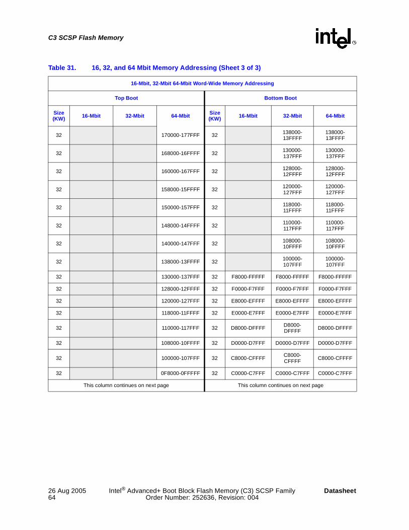
C3 SCSP Flash Memory
26 Aug 2005 Intel® Advanced+ Boot Block Flash Memory (C3) SCSP Family Datasheet64 Order Number: 252636, Revision: 004
32 170000-177FFF 32 138000-13FFFF
138000-13FFFF
32 168000-16FFFF 32 130000-137FFF
130000-137FFF
32 160000-167FFF 32 128000-12FFFF
128000-12FFFF
32 158000-15FFFF 32 120000-127FFF
120000-127FFF
32 150000-157FFF 32 118000-11FFFF
118000-11FFFF
32 148000-14FFFF 32 110000-117FFF
110000-117FFF
32 140000-147FFF 32 108000-10FFFF
108000-10FFFF
32 138000-13FFFF 32 100000-107FFF
100000-107FFF
32 130000-137FFF 32 F8000-FFFFF F8000-FFFFF F8000-FFFFF
32 128000-12FFFF 32 F0000-F7FFF F0000-F7FFF F0000-F7FFF
32 120000-127FFF 32 E8000-EFFFF E8000-EFFFF E8000-EFFFF
32 118000-11FFFF 32 E0000-E7FFF E0000-E7FFF E0000-E7FFF
32 110000-117FFF 32 D8000-DFFFF D8000-DFFFF D8000-DFFFF
32 108000-10FFFF 32 D0000-D7FFF D0000-D7FFF D0000-D7FFF
32 100000-107FFF 32 C8000-CFFFF C8000-CFFFF C8000-CFFFF
32 0F8000-0FFFFF 32 C0000-C7FFF C0000-C7FFF C0000-C7FFF
This column continues on next page This column continues on next page
Table 31. 16, 32, and 64 Mbit Memory Addressing (Sheet 3 of 3)
16-Mbit, 32-Mbit 64-Mbit Word-Wide Memory Addressing
Top Boot Bottom Boot
Size(KW) 16-Mbit 32-Mbit 64-Mbit Size
(KW) 16-Mbit 32-Mbit 64-Mbit

C3 SCSP Flash Memory
Datasheet Intel® Advanced+ Boot Block Flash Memory (C3) SCSP Family 26 Aug 2005Order Number: 252636, Revision: 004 65
Table 32. 16, 32, and 64 Mbit Memory Addressing (Sheet 1 of 2)
16-Mbit, 32-Mbit 64-Mbit Word-Wide Memory Addressing
Top Boot Bottom Boot
Size(KW) 16-Mbit 32-Mbit 64-Mbit Size
(KW) 16-Mbit 32-Mbit 64-Mbit
32 0F0000-0F7FFF 32 B8000-BFFFF B8000-BFFFF B8000-BFFFF
32 0E8000-0EFFFF 32 B0000-B7FFF B0000-B7FFF B0000-B7FFF
32 0E0000-0E7FFF 32 A8000-AFFFF A8000-AFFFF A8000-AFFFF
32 0D8000-0DFFFF 32 A0000-A7FFF A0000-A7FFF A0000-A7FFF
32 0D0000-0D7FFF 32 98000-9FFFF 98000-9FFFF 98000-9FFFF
32 0C8000-0CFFFF 32 90000-97FFF 90000-97FFF 90000-97FFF
32 0C0000-0C7FFF 32 88000-8FFFF 88000-8FFFF 88000-8FFFF
32 0B8000-0BFFFF 32 80000-87FFF 80000-87FFF 80000-87FFF
32 0B0000-0B7FFF 32 78000-7FFFF 78000-7FFFF 78000-7FFFF
32 0A8000-0AFFFF 32 70000-77FFF 70000-77FFF 70000-77FFF
32 0A0000-0A7FFF 32 68000-6FFFF 68000-6FFFF 68000-6FFFF
32 098000-09FFFF 32 60000-67FFF 60000-67FFF 60000-67FFF
32 090000-097FFF 32 58000-5FFFF 58000-5FFFF 58000-5FFFF
32 088000-08FFFF 32 50000-57FFF 50000-57FFF 50000-57FFF
32 080000-087FFF 32 48000-4FFFF 48000-4FFFF 48000-4FFFF
32 078000-07FFFF 32 40000-47FFF 40000-47FFF 40000-47FFF
32 070000-077FFF 32 38000-3FFFF 38000-3FFFF 38000-3FFFF
32 068000-06FFFF 32 30000-37FFF 30000-37FFF 30000-37FFF
32 060000-067FFF 32 28000-2FFFF 28000-2FFFF 28000-2FFFF
32 058000-05FFFF 32 20000-27FFF 20000-27FFF 20000-27FFF
32 050000-057FFF 32 18000-1FFFF 18000-1FFFF 18000-1FFFF
32 048000-04FFFF 32 10000-17FFF 10000-17FFF 10000-17FFF
32 040000-047FFF 32 08000-0FFFF 08000-0FFFF 08000-0FFFF
32 038000-03FFFF 4 07000-07FFF 07000-07FFF 07000-07FFF

C3 SCSP Flash Memory
26 Aug 2005 Intel® Advanced+ Boot Block Flash Memory (C3) SCSP Family Datasheet66 Order Number: 252636, Revision: 004
Appendix D Device ID Table
32 030000-037FFF 4 06000-06FFF 06000-06FFF 06000-06FFF
32 028000-02FFFF 4 05000-05FFF 05000-05FFF 05000-05FFF
32 020000-027FFF 4 04000-04FFF 04000-04FFF 04000-04FFF
32 018000-01FFFF 4 03000-03FFF 03000-03FFF 03000-03FFF
32 010000-017FFF 4 02000-02FFF 02000-02FFF 02000-02FFF
32 008000-00FFFF 4 01000-01FFF 01000-01FFF 01000-01FFF
32 000000-007FFF 4 00000-00FFF 00000-00FFF 00000-00FFF
Table 33. Device ID
Read Configuration Address and Data
Item Address Data
Manufacturer Code x16 00000 0089
Device Code
16-Mbit x 16-T x16 00001 88C2
16-Mbit x 16-B x16 00001 88C3
32-Mbit x 16-T x16 00001 88C4
32-Mbit x 16-B x16 00001 88C5
Note: Other locations within the configuration address space are reserved by Intel for future use.
Table 32. 16, 32, and 64 Mbit Memory Addressing (Sheet 2 of 2)
16-Mbit, 32-Mbit 64-Mbit Word-Wide Memory Addressing
Top Boot Bottom Boot
Size(KW) 16-Mbit 32-Mbit 64-Mbit Size
(KW) 16-Mbit 32-Mbit 64-Mbit

C3 SCSP Flash Memory
Datasheet Intel® Advanced+ Boot Block Flash Memory (C3) SCSP Family 26 Aug 2005Order Number: 252636, Revision: 004 67
Appendix E Protection Register Addressing
Table 34. Protection Register Addressing
Word-Wide Protection Register Addressing
Word Use A7 A6 A5 A4 A3 A2 A1 A0
LOCK Both 1 0 0 0 0 0 0 0
0 Factory 1 0 0 0 0 0 0 1
1 Factory 1 0 0 0 0 0 1 0
2 Factory 1 0 0 0 0 0 1 1
3 Factory 1 0 0 0 0 1 0 0
4 User 1 0 0 0 0 1 0 1
5 User 1 0 0 0 0 1 1 0
6 User 1 0 0 0 0 1 1 1
7 User 1 0 0 0 1 0 0 0
Note: All address lines not specified in the above table must be 0 when accessing the Protection Register—for example, A21–A8 = 0.

C3 SCSP Flash Memory
26 Aug 2005 Intel® Advanced+ Boot Block Flash Memory (C3) SCSP Family Datasheet68 Order Number: 252636, Revision: 004
Appendix F Mechanical and Shipping Media Details
F.8 Mechanical Specification
Note: Shaded pins indicate upper address balls for 64-Mbit and 128-Mbit devices. In all Flash and SRAM combinations, 66 balls are populated on lower density devices. (Upper address balls are not populated).
E
1 2 3 4 5 6 7 8
A
B
C
D
E
F
G
H
9 10 11 12
A1Index
D
12345678
A
B
C
D
E
F
G
H
9101112
S2
S1
b
e
Bottom View - Ball UpTop View - Ball Down
AA2
Y
A1
Table 35. Packaging Specifications (0.18µm and 0.25µm) (Sheet 1 of 2)
Millimeters Inches
Sym Min Nom Max Min Nom Max
Package Height A 1. 400 0.0551
Ball Height A1 0.250 0.0098
Package Body Thickness A2 0.960 0.0378
Ball Lead Diameter b 0.350 0.400 0.450 0.0138 0.0157 0.0177
Package Body Length – 16-Mbit/2-Mbit
D
9.900 10.00 10.100 0.3898 0.3937 0.3976
Package Body Length –
32-Mbit/4-Mbit, 16-Mbit/4-Mbit11.900 12.000 12.100 0.4685 0.4724 0.4764
Package Body Length –
32-Mbit/8-Mbit 13.900 14.000 14.100 0.5472 0.5512 0.5551
Package Body Width –
16-Mbit/2-Mbit, 16-Mbit/4-Mbit,
32-Mbit/4-Mbit, 32-Mbit/8-Mbit
E 7.900 8.000 8.100 0.3110 0.3150 0.3189

C3 SCSP Flash Memory
Datasheet Intel® Advanced+ Boot Block Flash Memory (C3) SCSP Family 26 Aug 2005Order Number: 252636, Revision: 004 69
Pitch e 0.800 0.0315
Ball (Lead) Count N 66 66
Seating Plane Coplanarity Y 0.100 0.0039
Corner to Ball A1 Distance Along E16-Mbit/2-Mbit, 16-Mbit/4-Mbit,
32-Mbit/4-Mbit, 32-Mbit/8-Mbit
S1 1.100 1.200 1.300 0.0433 0.0472 0.0512
Corner to Ball A1 Distance Along D
16-Mbit/2-Mbit
S2
0.500 0.600 0.700 0.0197 0.0236 0.0276
Corner to Ball A1 Distance Along D
32-Mbit/4-Mbit, 16-Mbit/4-Mbit1.500 1.600 1.700 0.0591 0.0630 0.0669
Corner to Ball A1 Distance Along D
32-Mbit/8-Mbit2.500 2.600 2.700 0.0984 0.1024 0.1063
Table 35. Packaging Specifications (0.18µm and 0.25µm) (Sheet 2 of 2)
Millimeters Inches
Sym Min Nom Max Min Nom Max

C3 SCSP Flash Memory
26 Aug 2005 Intel® Advanced+ Boot Block Flash Memory (C3) SCSP Family Datasheet70 Order Number: 252636, Revision: 004
Table 36. Packaging Specifications (0.13µm)
Millimeters Inches
Sym Min Nom Max Min Nom Max
Package Height
16/02-Mb, 16/04-Mb, 32/08-MbA
1. 200 0.0472
Package Height
32/04-Mb1. 400 0.0551
Ball Height
16/02-Mb, 16/04-Mb, 32/08-MbA1
0.200 0.0079
Ball Height
32/04-Mb0.250 0.0098
Package Body Thickness
16/02-Mb, 16/04-Mb, 32/08-MbA2
0.860 0.0339
Package Body Thickness
32/04-Mb0.960 0.0378
Ball (Lead) Width
16/02-Mb, 16/04-Mb, 32/08-Mbb
0.325 0.375 0.425 0.0128 0.0148 0.0167
Ball (Lead) Width
32/04-Mb0.350 0.40 0.450 0.0138 0.0157 0.0177
Package Body Length
16/02-Mb, 16/04-MbD
9.900 10.000 10.100 0.3898 0.3937 0.3976
Package Body Length
32/04-Mb, 32/08-Mb11.900 12.000 12.100 0.4685 0.4724 0.4764
Package Body Width
16/02-Mb, 16/04-Mb, 32/04-Mb, 32/08-MbE 7.900 8.000 8.100 0.3110 0.3150 0.3189
Pitch e 0.800 0.0315
Ball (Lead) Count N 66 66
Seating Plane Coplanarity Y 0.100 0.0039
Corner to Ball A1 Distance Along E
16/02-Mb, 16/04-Mb, 32/04-Mb, 32/08-MbS1 1.100 1.200 1.300 0.0433 0.0472 0.0512
Corner to Ball A1 Distance Along D
16/02-Mb, 16/04-MbS2 0.500 0.600 0.700 0.0197 0.0236 0.0276
Corner to Ball A1 Distance Along D
32/04-Mb, 32/08-MbS2 1.500 1.600 1.700 0.0591 0.0630 0.0669

C3 SCSP Flash Memory
Datasheet Intel® Advanced+ Boot Block Flash Memory (C3) SCSP Family 26 Aug 2005Order Number: 252636, Revision: 004 71
F.9 Media Information
Note: Top view, ball side down. Drawing is not to scale and is only designed to show orientation of devices.
Tray Chamfer
Device Pin 1

C3 SCSP Flash Memory
26 Aug 2005 Intel® Advanced+ Boot Block Flash Memory (C3) SCSP Family Datasheet72 Order Number: 252636, Revision: 004
Note: Top view, ball side down.
Figure 21. SCSP Device in 24 mm Tape (10 mm x 8 mm and 12 mm x 8 mm)
Device Pin 1

C3 SCSP Flash Memory
Datasheet Intel® Advanced+ Boot Block Flash Memory (C3) SCSP Family 26 Aug 2005Order Number: 252636, Revision: 004 73
Appendix G Additional Information
Table 37. Related Documents
Order Number Document/Tool
292216 AP-658 Designing for Upgrade to the Advanced+ Boot Block Flash Memory
292215 AP-657 Designing with the Advanced+ Boot Block Flash Memory Architecture
Contact Your Intel Representative Flash Data Integrator (FDI) Software Developer’s Kit
297874 FDI Interactive: Play with Intel’s Flash Data Integrator on Your PC
Notes:1. Please call the Intel Literature Center at (800) 548-4725 to request Intel documentation.
International customers should contact their local Intel or distribution sales office.2. Visit Intel’s World Wide Web home page at http://www.Intel.com or http://developer.intel.com for
technical documentation and tools.

C3 SCSP Flash Memory
26 Aug 2005 Intel® Advanced+ Boot Block Flash Memory (C3) SCSP Family Datasheet74 Order Number: 252636, Revision: 004
Appendix H Ordering Information
.
Table 38. Ordering Information for Product Combinations with 0.25 µm to 0.13 µm Flash
Table 39. Ordering Information for Combinations specific to 32M 0.13 µm Flash
R D 2 8 F 1 6 0 2 C 3 T D 7 0
PackageRD = Leaded Ball Stacked -CSP
Product Line Designator
16 Mbit = 70, 90, or 110 ns32 Mbit = 70 or 90 ns
Access Speed (ns)
28F or 38F = Intel® Flash Memory
Flash Density320 = x16 (32 Mbit)160 = x16 (16 Mbit)
SRAM Device Density8 = x16 (8 Mbit)4 = x16 (4 Mbit)2 = x16 (2 Mbit)
Parameter LocationT = Top BlockingB = Bottom Blocking
D = 0.13µm<blank> = 0.25µm or 0.18µm (refer to access speed for differientation)
Technology Differentiator
C = Advanced+ Boot Block Flash Memory
Product Family
PF = Lead-Free Ball Stacked-CSP
Parameter Location
R D 3 8 F 1 0 1 0 C 0 Z T L 0
PackageRD = Leaded Ball Stacked-CSP
Product Line Designator
DensityFlash #1 = 1 = 32 MbitFlash #2 = 0 = No DieFlash #3 = 1 = 4 Mbit SRAM = 2 = 8 Mbit SRAM Flash #4 = 0 = No Die
Product Family
0 = Original Version ofthis product:Flash Speed = 70 nsFlash Process = 0.13 µmVccq = 2.7 V to 3.3 V
Device Details
L = 72 ball "I"-balloutPinout Indicator
T = Top BlockingB = Bottom Blocking
VoltageZ = 3.0V I/O
C = Advanced+ Boot Block Flash Memory
38F = Intel Flash Stacked Memory®
PF = Lead-Free Ball Stacked-CSP

C3 SCSP Flash Memory
Datasheet Intel® Advanced+ Boot Block Flash Memory (C3) SCSP Family 26 Aug 2005Order Number: 252636, Revision: 004 75
Table 40. Ordering Information Valid Combinations
0.25µm C3 SCSP 0.18µm C3 SCSP 0.13µm C3 SCSP
32-Mbit No longer available.
RD28F3208C3T70
RD28F3208C3B70
RD28F3208C3T90
RD28F3208C3B90
RD28F3204C3T70
RD28F3204C3B70
RD38F1010C0ZTL0
RD38F1010C0ZBL0
PF38F1010C0ZTL0
PF38F1010C0ZBL0
RD38F1020C0ZTL0
RD38F1020C0ZBL0
16-Mbit
RD28F1604C3T90
RD28F1604C3B90
RD28F1604C3T110
RD28F1604C3B110
RD28F1602C3T90
RD28F1602C3B90
RD28F1602C3T110
RD28F1602C3B110
RD28F1602C3T70
RD28F1602C3B70
PF28F1602C3TD70
RD28F1602C3TD70
RD28F1602C3BD70
RD28F1604C3TD70
RD28F1604C3BD70