integrated power & energy efficiency - catrene,...
TRANSCRIPT

Catrene Scientific Committee Working Group: Integrated power & energy efficiency
Integrated power & energy efficiency
Power device technologies, simulations, assembly and circuit topographies enabling
high energy efficiency applications

Integrated power & energy efficiency ii
Integrated power & energy efficiency committee members
Prof. Gaudenzio Meneghesso (UniPD - IUNET) – Coordinator Working group members: Dr. Anton Bauer (Fraunhofer IISB) Prof. Braham Ferreira (TU DELFT) Dr. Jean-Pierre Ganne (Thales Research & Technology) Dr. Renaud Gillon (On-Semi) Thomas Harder (General Manager ECPE) Dr. Eckart Hoene (Fraunhofer IZM) Dr. Jürgen Lorenz (Fraunhofer IISB) Dr. Peter Moens (On-Semi - B) Prof. Mikael Östling (KTH) Dr. Jelena Popovic (TUDelft) Dr. Jan Sonsky (NXP - Belgium) Dr. Renaud Stevens (SOITEC) Dr. Steve Stoffels (IMEC) Other contributors:
Dr. Oliver Ambacher (IAF) Dr. Jean-Jacques Aubert (CEA-Leti) Dr. Filip Bauwens (ONSemi) Dr. Marco Camalleri (STMicro) Dr. Wolfgang Dettmann (Infineon) Dr. Peter Friedrichs (Infineon) Dr. Klaus Heyers (Bosch GmbH) Dr. Richard Lebourgeois (Thales) Prof. Leo Lorenz (President ECPE) Dr. Angelo Magrì (ST Micro) Dr. Frans Pansier (NXP)
Dr. Alfonso Patti (STMicro) Dr. Joachim Pelka (Fraunhofer VµE) Caroline Perfetti (Soitec)) Dr. Martin Rambach (Bosch) Daniel Rondi (Soitec) Dr. Matthias Rose (NXP) Dr. Phil Rutter (NXP) Dr. Lothar Schindele (Bosch GmbH) Yann Sinquin (Soitec) Dr. Daan van Wyk (UJ) Prof. Enrico Zanoni (University of Padova)

Catrene Scientific Committee Working Group: Integrated power & energy efficiency
Summary Integrated power & energy efficiency committee members ................................................. ii 1. Abstract ..................................................................................................................... 1 2. Executive Summary ................................................................................................... 2 3. Section 1: Power electronics enabling energy efficiency ............................................ 10
Energy Savings Potential ........................................................................................... 10 Energy supply and CO2 emissions ..................................................................................................... 11 Role of power electronics in improving energy efficiency in key applications ................................... 11 Power electronics in the global view ................................................................................................. 13 Conclusions ...................................................................................................................................... 16
4. Section 2: Power devices ......................................................................................... 17 Figure of merit and Benchmarking Power- Si – SiC – GaN ........................................ 17
Electrical parameters ......................................................................................................................... 18 Power transistor figures of merit ....................................................................................................... 20 Benchmarking ................................................................................................................................... 21 Conclusion ........................................................................................................................................ 22
Si –Power devices ...................................................................................................... 26 Discrete vs. Integrated Power Devices .............................................................................................. 26 Low Voltage MOSFETs .................................................................................................................... 28 High Voltage MOSFETs ................................................................................................................... 31 IGBTs ............................................................................................................................................... 34 Device vs. Application landscape ...................................................................................................... 35 Si-power Devices, key topics & requirements for future funded projects: .......................................... 36
SiC Power semiconductor devices ............................................................................. 38 Introduction ...................................................................................................................................... 38 High voltage blocking ....................................................................................................................... 40 SiC diodes/rectifiers ......................................................................................................................... 40 Switch devices .................................................................................................................................. 40 JFETs ............................................................................................................................................... 41 MOSFETs ......................................................................................................................................... 41 Bipolar Junction Transistors ............................................................................................................. 41 Very High Voltage - High Injection Devices ..................................................................................... 42 Concluding remarks and Issues of concerns for SiC power devices ................................................... 42
Power GaN Device Technology ................................................................................. 44 GaN material and device physics ...................................................................................................... 45

Integrated power & energy efficiency ii
Device architectures .......................................................................................................................... 47 Ohmic contacts ................................................................................................................................. 48 E-mode devices ................................................................................................................................. 48 Breakdown voltage engineering and limitations ................................................................................ 50 Conclusion ........................................................................................................................................ 51
New materials and Substrates for WBG power devices ............................................. 56 State of the art of the existing substrates for power devices ............................................................... 56 Supply Chain of GaN and SiC substrates .......................................................................................... 58 Large GaN-on-Si substrates .............................................................................................................. 60 Advanced substrates .......................................................................................................................... 64 Innovation through layer transfer technologies ................................................................................. 65
Simulation of Power devices ...................................................................................... 67 Process Simulation ............................................................................................................................ 68 Device Simulation ............................................................................................................................. 70 Mixed-Mode simulations .................................................................................................................. 71 Circuit Simulation ............................................................................................................................ 72 Conclusion ........................................................................................................................................ 73
Reliability issues in Si-Power devices ........................................................................ 74 Overview of Power MOSFET reliability and qualification testing .................................................... 74 Oxide Reliability Effects. .................................................................................................................. 76 Thermally Induced Degradation and Failure. .................................................................................... 79 Interaction Mold Compound—Si Structure. ..................................................................................... 80 Silicon Defects. ................................................................................................................................. 82 Radiation Hardness ........................................................................................................................... 84 Conclusion ........................................................................................................................................ 86
Reliability issues in SiC power devices ...................................................................... 88 Intrinsic defects ................................................................................................................................. 89 Gate oxide stability ........................................................................................................................... 90 Contact and metallization stability ................................................................................................... 92 High temperature stability ................................................................................................................ 92
Reliability issues in GaN power devices .................................................................... 93 Parasitic and dispersion effects: ........................................................................................................ 93 Reliability issues ............................................................................................................................... 98
High temperature performances, thermal management, Limits of High temperature operation ................................................................................................................. 106
Wide bandgap devices ..................................................................................................................... 106 High temperature packaging ........................................................................................................... 109 High temperature Gate drives ......................................................................................................... 110

Integrated power & energy efficiency ii
Passives for High Temperature Power Electronics .......................................................................... 110 Packaging issues and solutions for Power devices .................................................... 113
New packaging technologies for high power modules ..................................................................... 113 High efficient double sided cooling technology (for E-Mobility) ..................................................... 114 Embedding ...................................................................................................................................... 114 Die attach ....................................................................................................................................... 115 Top side interconnects .................................................................................................................... 115 Encapsulation ................................................................................................................................. 115
High power Passives for Inverter / Converter ......................................................... 116 Magnetic components and frequency evolution of SMPS (from kHz to multi MHz) ........................ 116 Trends in the evolution of magnetic components ............................................................................ 119 Research directions on high frequency passive components: four challenges. .................................. 120
5. Section 3: Integrated Power and Efficient conversion circuits ................................. 122 Integration of WB devices into systems and circuits ................................................ 122
Alternative approaches are needed to system design ....................................................................... 123 Capacitive effects and issues ........................................................................................................... 124 Evolution of existing technology platforms ..................................................................................... 124 Bridging the gap between power and RF electronics ....................................................................... 125 High temperature operation ............................................................................................................ 125
Gate drivers (co-integration) (GaN) ........................................................................ 126 GaN gate driver requirements ......................................................................................................... 126 Monolithic integration approaches ................................................................................................. 129 Heterogenous integration ................................................................................................................ 131 GaN drivers and GaN co-integration, key topics & requirements for future funded projects ........... 131
Thermal design and thermal management ................................................................ 132 Spreading the heat of small WBG dies ............................................................................................ 132 Thermal management vs. high frequency operation ........................................................................ 133 New thermal management design approaches ................................................................................. 133 High temperature operation ............................................................................................................ 134 Thermal management of passives .................................................................................................... 134 Market penetration ......................................................................................................................... 134
EMC of power devices ............................................................................................. 135

Integrated power & energy efficiency 1
1. Abstract Today already 40% of the world wide used energy is provided by electric power. It is
expected that this share is going to rise to about 60% by 2040. This enormous amount of energy not only needs to be produced environmentally friendly, but it also should be distributed and used efficiently. For that, power electronic devices, circuits, modules and systems are needed in large numbers, so that, depending on the application, the suitable electric current electric voltage and frequency profile can be produced. The goal is to consequently minimize the dissipation factor and the production costs of these devices. The introduction of efficient power electronics in the fields of renewable energies and automobile electronics, can, by itself, enable possible energy savings from 20 to 35%. Innovations span from new advanced semiconductor materials, like a promising class of novel wide bandgap semiconductors (WBS), to new device technologies (advanced Si, vertical and lateral structures, etc.) to innovative circuit and system solution able to optimize energy conversion, energy storage, energy distribution and finally energy usage.
European industry and academia are amongst the global leaders in the complex More Than Moore technologies for the power electronic devices and Europe is leading in measures towards reducing green house gas emissions. This perfect match of technological leadership and ambitious societal targets could be leveraged by European and national funding for power electronic devices and technologies. Collaborative projects will strengthen the European industrial and academic landscape by securing and generating employment in a key enabling technology domain enabling energy efficient solutions for the future.
The scope of this document is to present the state of the art of the available power devices, highlight the main potential and limitation and indicate the path for the future materials and device technology that will be required to meet the request for a green energy world. Starting with a general introduction on the role of power electronics in improving energy efficiency, a summary of the main advances in device technology will then been presented. Advanced new Si technologies, new power device based on Silicon Carbide (SiC) and Gallium Nitride (GaN) will be described in detail together with a benchmark of the different technologies, highlighting the main potential and limitation of the different technologies. Indeed, TCAD simulation tools will play a crucial role for the development of highly performing, robust and reliable power devices, and for this reason a section is dedicated also to this topic. The main challenges for the availability of new materials and new substrates will be discussed. These materials and substrates need to be available with very high quality and at very low cost. Then, reliability issues of the different power devices technologies (Si, SiC and GaN) will be presented. This study will highlight the main issues, which are limiting the production of reliable devices in applications where, next to efficiency, also reliability is a must (automotive, satellite, …). Furthermore, passive devices and packaging will very likely present the main bottleneck for exploiting the full capabilities of future WBS devices, and will require the development of new concepts ; these aspects will be discussed in the two specific sessions. Finally, the main open issues for the integration of wide band gap semiconductors devices in in systems will also be discussed with specific attention to thermal management and electromagnetic interference and immunity.
This document is the result of the work of many European researchers either from industrial and academic research centers, that have decided to produce a document that hopefully will represent a starting point for those who would like to know about the development of power technologies for the implementation of very high efficient systems. To facilitate the reader, an executive summary reporting the main point collected in this document, is presented in the following pages.

Integrated power & energy efficiency
2
2. Executive Summary Energy Savings Potential
Power Electronics is the technology associated with the efficient conversion, control and conditioning of electric energy from the source to the load. It is the enabling technology for the generation, distribution and efficient use of electrical energy. It is a cross-functional technology covering the very high Giga Watt (GW) power (e.g. in energy transmission lines) down to the very low milliWatt (mW) power needed to operate a mobile phone. Many market segments such as domestic and office appliances, computer and communication, ventilation, air conditioning and lighting, factory automation and drives, traction, automotive and renewable energy, can potentially benefit from the application of power electronics technology. The ambitious goals of the European Union to reduce the energy consumption and CO2 emissions can only be achieved by an extensive application and use of Power Electronics, as power electronics is the basic prerequisite for:
• Efficiently feeding-in wind and solar energy to the grids; • The stabilization of the power grids with increasing share of fluctuating renewable energies; • Highly efficient variable speed motor drives; • Energy efficient and low-emission mobility with hybrid and full electric vehicles; • An energy saving lighting technology; • Efficient recovery of braking energy; • Energy management of batteries; • Control appliances and building management systems via the grid interface (smart grids).
The estimated energy savings potential that can be achieved by introducing power electronics into systems is enormous, more than 25% of the current electricity consumption in the EU countries. Since power electronics is a key technology in achieving a sustainable energy society, the demand for power electronics solutions will show significant growth in the coming decades. The European industry holds a strong position in the field of power semiconductors and modules and is establishing a wide band-gap semiconductors technology base. Europe also has high quality power electronics research groups at universities and research institutes with well-established networks and associations in Europe to provide platforms for discussion, cooperation and joint research. On the other hand, outsourcing of research and technology to other countries (not only Japan, USA, but also emerging countries), strong research increment in these countries, and the possibility of key European companies being taken over by competitors from Asia, make it even more critical for Europe to keep up with the technological development. This requires continuous investments in research and development.
Benchmarking In this section the most important figure of merit for switching power are reported for the
latest generation of power components on the market, and this for different competing technologies. It is shown that the FOM for silicon technologies are close to material dictated limits and it will be hard and expensive to get further incremental improvements in performance. GaN and SiC on the other hand are disruptive technologies that offer orders of magnitude better FOM’s than silicon. First generation products already show figures of merit, which are a factor 4 to 5 better than the latest generation of silicon technologies, with much headroom for future improvements. For GaN the biggest gain for the FOM is currently achieved in the medium voltage range (200V-600V), while for the low voltage range the contact resistance needs to come down further and currently puts a limit on the low voltage FOM. SiC on the other hand is currently only available for the higher end of the medium voltage range (1200V), due to its high cost, which makes it difficult to compete in the lower voltage ranges. Investment in GaN should focus on optimizing it’s advantage in the medium power range and driving the cost of the products down to compete more easily in this market. The medium voltage range houses market segment such as
Integrated power & energy efficiency
3
home appliances and consumer electronics and thus present a huge potential market opportunity.At the same time effort should be spend on lowering the contact resistances in the GaN material to allow penetration of the technology in the lower voltage ranges, where there is a huge market for switched mode power supplies for IT and servers. SiC should leverage its strength at the high voltage ranges. Power transmission and large electrical engines such as locomotives should be a potential market and funding should focus on developing SiC technology to displace established IGBT’s and Thyristors in this voltage range.
Si –Power devices Si power devices have evolved over last several decades and dedicated device structures were
engineered for different voltage classes. Along the way, numerous innovations have been realized to improve different aspects of device performance often beyond the so-called silicon-material-limits. This chapter will start with discussion of key differences between discrete and integrated power devices and the following sub-sections will zoom-in to different available discrete technologies, including Low Voltage MOSFETs, High Voltage MOSFETs and IGBTs. Each section will cover key device types and innovation trends, including comparative performance assessment of the different competing components. Secondly the essential manufacturing technologies required to produce the different components will be discussed. Thirdly typical failure modes and reliability aspects specific to each technology type will be addressed. Finally fundamental performance limitations will be outlined. This will provide a good link to the other parts of the report discussing potential of wideband-gap based power components. As the device scaling continues, higher switching frequency is utilized and operating temperature increases, one of the innovation trends is towards so-called “smart discrete”. These are components with on-chip integrated self-protection components. This part of the report will conclude with mapping the different power components and technologies on applications and circuit topologies.
SiC Power semiconductor devices This subsection will focus on the state of the art in silicon carbide power device technology.
A general overview will be presented on the status of silicon carbide wafer quality and availability. A brief discussion on possible switching speed advantage by using SiC devices vs traditional Si devices will be included. Size and weight advantages will be demonstrated. The second part will focus on current and future MOSFET devices. Fabrication strategies as well as a discussion on fundamental and practical performance limitations are included. A special focus will be on oxide properties and hence channel mobility. The third part is devoted to JFET devices and fabrication strategies. Current device ratings and availability as well as device types are discussed. Both normally-on and normally-off devices will be discussed as well as high temperature properties. The fourth part concerns bipolar junction transistors. Also here current fabrication strategies and device designs will be explored. A paragraph will also be devoted to operation under harsh environments. High voltage design above 3 kV will be included as well as high voltage junction termination extension structures.
Power GaN Device Technology The research and development of GaN technology for power switching has made large
strides in the past decade, several key challenges have been addresses since the inception of GaN as a power technology. To succeed as a power technology, the transistors need to exhibit a high breakdown voltage, a low on-resistance, a low leakage current a positive threshold voltage, high stability, reliability and should be cost competitive (at least at system level) with established silicon technologies. It has been shown by several research labs, universities and companies that GaN components do exhibit figures of merit which are an order of magnitude better than what is achievable with silicon and even SiC. However several key issues remain. Beyond the obvious challenge of scaling the technology to higher breakdown voltages and power levels, there were some other less obvious challenges. Historically GaN HEMT’s were grown on a SiC substrate. The high price of this solution would make it difficult for GaN to compete in the world of power
Integrated power & energy efficiency
4
electronics. To address this issue, researchers have introduced the GaN-on-Si technology which removed the expensive SiC substrate and leveraged the industrial strength of the large install base of silicon fabs. To ensure CMOS compatibility, necessary for processing in a silicon fab, all Au containing steps had to be removed from the process. This has meant a re-optimization of the ohmic contacts with silicon compatible metals. To secure the leadership of Europe in GaN technology, we need to make sure that we leverage the strength and cost competiveness of the GaN-on-Si technology and make targeted investments to bring this technology further along in its maturity level. An important step in reducing the overall costs of production is scaling up the wafer size to 200mm. First demonstrators have been shown on 200mm wafers, but further optimization is needed to increase yield, assess reliability and evaluate proper packaging techniques for these components. Furthermore, the ohmic metal stack and gate metal stack should be re-optimized to ensure silicon compatibility, while at the same time showing reproducibility, stability and a good performance. Contact resistance and gate leakage are key metrics for this optimization. Also, functional demonstrators for target applications would make a strong case for field testing the technology and identifying key issues in early stage of development. Currently the only GaN devices on the market (EPC) have a maximum breakdown voltage of 200V. To capture larger portions of the market and assure market leading performance in 90% of the power market, it would be necessary to scale up the technology to at least 600V. Demonstrates in literature have shown breakdown voltages of 2000V, with record RonQg products, an order of magnitude below silicon. However, none of these technologies have been proven outside of research labs, and use tricks that might not be suited for large scale fabrication. Moreover, reliability and high voltage dispersion data has not been presented for these components and should all be addressed before high voltage GaN components can be introduced in the market. If Europe wants to play a leading role in this market, these issues should be addressed. A final challenge for GaN devices, which would require dedicated research and investment is in achieving true enhancement-mode (e-mode, normally off) operation. GaN devices are naturally depletion mode (d-mode), which means that in the case of a gate driver failure, the device will conduct current, potentially destroying the entire system. This mode of operation is not preferred by system designers, who prefer e-mode. Currently manufacturers prefer to couple a well-developed d-mode device with a low voltage silicon component in series. However, a high performance e-mode device would be the preferred solution from cost and performance perspective. If Europe wants to play a role in the future of GaN, resources should be spent on achieving reliable GaN transistors, with low on-state resistance and true e-mode operation. Several companies in US and Asia are heavily investigating these devices; therefore Europe cannot afford to miss the train.
New materials and Substrates for WBG power devices As the electrical power supply demand is increasing with the generalization of electric
devices in the consumer market, the challenge of the power management is to provide highly efficient components that reduce the power loss in all conversion steps needed in between electrical power generation, electrical transportation and final power use. To answer the technical challenges for high efficiency and small form factor, wide band gap material are gaining strong interest, in particular Gallium Nitride material (GaN) that enables performance breakthrough in key parameter devices compared to the established Si based devices. A number of challenges are however associated with the development of efficient GaN substrates, the first being a limited offer for industrial epitaxial GaN wafers in Europe at the moment. On top of this, there are currently no substrates at market compatible price for the next generation device with high performances, which will require a better material quality. This limits the innovation of European industrial power devices makers. Finally, typical key players in automotive or energy conversion are expecting the emergence of reliable GaN substrate providers to secure the global supply chain and allow the development of new innovative and competitive devices. New advanced substrates based on customized thin film stacking technologies could give access to high performance, flexible and thick GaN and overcome the challenges of directivity and dislocations due to lattice matching and

Integrated power & energy efficiency
5
thermal expansion variation. In this chapter WBG material and substrates for power devices will be described, focusing more specifically on the 2 most widely used, SiC and GaN. In the first section, the various existing technologies will be reviewed and assessed, and the inherent properties of materials such as SiC and GaN will be discussed. The key aspect of the supply chain for SiC and GaN will be evaluated in the second section. The third section will focus on the large GaN on Silicon substrates. Finally, we will discuss the emergence of a new type of advanced substrates.
Simulation of Power devices It is common understanding in industry and research that TCAD simulations are an
invaluable mean to investigate and optimize new processes and devices and to identify and analyze factors that cause parametric yield loss in manufacturing, when new processes, new device architectures and/or new materials are introduced. Appropriate use of TCAD strongly contributes to the reduction of development times and costs, and to increasing product yield on a wide range of technologies. This very well justifies investment in the development of the models and tools needed to carry out the required simulation studies. Especially, new, extended or adapted physical models must be developed and be made available in the standard tools used in industry, in order to cope with the requirements of specific materials, processes and architectures used for power devices. Technology Computer Aided Design (TCAD) has during the last decades developed into a key tool to support the development and optimization of semiconductor technologies, devices and circuits. Its scope extends from the simulation of process equipment through simulation of processes and devices to the simulation of circuits and systems. It is based on a thorough understanding of the physical effects involved at all these levels, the extraction of the required physical parameters, and the implementation of the models developed into simulation tools which enable an efficient and predictive simulation. The International Technology Roadmap for Semiconductors ITRS among others also contains a chapter on Modeling and Simulation. This chapter gives an estimate of about one third for the reduction of development times and costs for best practice cases in nanoelectronics. This should also be the aim for power electronics. Because the core of simulation comprises quantitative physical understanding and efficient algorithms, leading-edge simulation tools are mostly quite generic and may be used for a large variety of processes and devices. The range of such applications spans from aggressively scaled memory and logic devices to RF and power devices. In this chapter, the main additional features needed for the simulation of power devices and their fabrication, as well as the state-of-the art in these areas, are summarized. Important additional requirements are identified in the areas of process, device and circuit simulation. As part of this, also the numerical algorithms are faced with additional challenges.
Reliability issues in Si-Power devices Today Si power devices and technologies are in the market for a very long time, and have
matured in terms of reliability and qualification level. Due to the very high quality of Si starting material, and the thermally, chemically and electrically stable SiO2 with low interface states, Si power device technologies are qualified for the most demanding markets, like e.g. automotive applications, achieving very low ppm levels. However, since Si power devices have to compete against wide bandgap devices based on SiC and GaN, both having superior material parameters, novel and more advanced structures and features have to be implemented to remain cost-competitive, e.g. trench gate structures, deep trench super-junction structures, thin wafer technology etc. These new features introduce new reliability challenges to be worked on and to improve: high quality gate oxides grown on trench sidewalls, and the subsequent acceleration testing and modeling; void free epitaxial growth in deep trench structures; strain management in thin Si fins. This section provides an overview of the most relevant reliability issues in Si based power devices (diodes, MOSFETs, IGBTs,…). Although Si technologies are well established and have proven long term reliability, some important reliability issues deserve further study and improvement, especially for high voltage devices. As many silicon-based power devices are MOS-type (power MOSFETs, IGBTs etc), and as power MOS devices have a large Si area (several mm2

Integrated power & energy efficiency
6
up to a few cm2), both intrinsic as well as extrinsic reliability of the dielectric is important. The former is especially true for high temperature operation, since power MOSFETs can reach high local junction temperatures, leading to an accelerated dielectric degradation. The latter is defect driven, and scales with the device area. On top, many novel Power MOSFETs and IGBTs have trench gates or trench super-junctions, so that oxide and interface quality on trench sidewalls is important. To account for the need of higher voltages in the Si-Power devices, very often as in the case of IGBTs and diodes, the Silicon background doping is severely lowered. This puts more constraints on the power limitations since a low current density in the device during switching can already destroy its avalanche ruggedness. This effect is well understood and some tricks exist to overcome the problem, e.g. introduction of buffer layers, injection of minority carriers, etc. However this always comes at a cost and thus avoiding the sensitivity towards destruction by low current density switching is favored. Materials with higher maximum electric field capability compared to Silicon are preferred in that respect. Additional reliability issues mainly include passivation integrity failures, due to the lack of sufficient screening of the mobile charges in the mold compound from the lowly doped epi layers in the device termination (HTRB and H3TRB testing), cracking of the passivation layers, and device parameters shifting upon avalanche conditions (repetitive UIS testing)
Reliability issues in SiC power devices Despite the fact, that power devices on 4H-SiC shows superior properties compared to
silicon due to its wider band gap, and that several devices, like Schottky-barrier-diodes, JFETs, MOSFETs etc., are already on the market for some time, the penetration of the power device market by SiC devices is not as strong as it should be. SiC power devices target next to others at uninterrupted power supplies, automotive, wind turbine, PV inverters or grid applications. Here the users of power devices for the power electronic systems are very conservative. Their main concern is next to the price, the reliability of the devices. Except the SB-diode, which is sold times without numbers, the other devices show no significant application in systems in the field so far and, therefore no thorough reliability data are available. This section will describe the reliability issues of 4H-SiC power devices. It is divided in four subsections. The first subsection will identify and describe defects in the 4H-SiC substrate and how they can propagate into the epitaxy layers or better how they can be reduced or even avoided by epitaxy. Here, also life-time enhancement in the bulk of the epi-layer will be considered. Key points are very high temperature sacrificial oxidation or carbon implantation with subsequent high temperature annealing to increase lifetime. Both, the appropriate epitaxy as well as additional carbon introduction can increase the minority carrier lifetime in pin-diodes significantly. The second subsection covers the stability of gate oxides in MOSFETs, but also, because the issues are comparable, the stability of oxide passivation in high power applications. Here, interface state densities and their influence on threshold voltage and on channel mobility is the biggest reliability issue in 4H-SiC power devices in and of itself. Furthermore, the build-up of charges in the oxide and the dielectric breakdown fields will be addressed. In the third subsection the reliability of Ohmic- as well as Schottky-contacts will be considered. If the interface between metallization and SiC is not perfectly smooth or the consistency of the used metal layers is not well controlled, phase separation or even precipitation in the contact metallization will occur which will negatively influence the device stability. In the last section the thermal stability will be addressed very briefly. Finally the following aspects will be covered: i) high temperature stability ii) reliability iii) availability of high temperature applicable packaging and assembly and iv) passives for high temperature.
Reliability issues in GaN power devices GaN High Electron Mobility Transistors are excellent devices for high power and high
frequency applications. Thanks to the advantageous material properties of GaN-based semiconductors, such devices will operate at very high drain voltages, where the extremely high electric fields drive high current densities in the two-dimensional channel electron gas at fairly high channel temperatures. The resulting operating conditions are by far more severe than those

Integrated power & energy efficiency
7
encountered by any other semiconductor developed so far. Even though significant improvements in the quality of GaN-related substrates and epitaxial structures have been achieved in the past few years, GaN based devices still have material-related issues which need to be resolved. This section will present an overview of the parasitic and reliability issues in Gallium Nitride-based transistors. From the parasitic point of view the following represent the main open issues related to the GaN-HEMTs technology: (i) trap-related effects leading to the deleterious dynamic RDSON (due to surface, interface, bulk traps), (ii) gate leakage current, (iii) kink phenomena. The effects of surface, interface and bulk traps will be discussed, on the basis of experimental data obtained by means of pulsed measurements, Deep Level Transient Spectroscopy, photocurrent spectroscopy and of 2D device simulation results. Reliability issues in GaN HEMTs devices will be also largely described. The main target of this section is to highlight the peculiarity of the degradation mechanism in these devices. In particular, it will be shown that new failure mechanisms are present in the devices based on this material system (gate edge degradation and semiconductor cracking), and also that many of the observed degradation mechanisms do not completely follow the typical activation energy law, that have been (and is nowadays) largely applied in Silicon power devices. Failure modes and mechanisms of GaN HEMTs will be critically reviewed, including the time-dependent gate leakage increase during reverse bias tests, hot-electron-induced drain current degradation, gate and ohmic contact degradation, delamination of passivation and electron trapping. Finally, a review of the most commonly known technological countermeasures for alleviating reliability issues will also be briefly described (Single and multiple field plate designs, Cap layer (thin GaN cap, p-type GaN cap, buffer optimization (heterostructure, Fe-doping etc), passivation (in-situ, ex-situ), MISHEMT structure versus Schottky-based HEMT etc.
High temperature performances, thermal management, high temperature operation Increasing the working temperature of power devices and modules is a key issue for
improving and simplifying the heat exchangers and cooling systems of power applications as well as for introducing power devices in high temperature environments such as deep drilling or aeronautics. New technologies around wide bandgap semiconductors, silicon carbide and gallium nitride mainly, are important breakthroughs to improve on the intrinsic temperature limitations of silicon technology. But, while the new materials themselves are able to stand very high operation temperatures, thermal limitations may still occur at the device level, the module level or the system level. At the device level, the diffusion processes can reduce the lifetime but the main issue will certainly appear at the metallization level, increasing electromigration and requiring a shift from aluminum to copper. At the module level, increasing the working temperature will require the removal of insulating gels and a change in the nature of the packaging polymers. Thermal management will be the key. At the system level, increasing working frequency and temperature at the same time as well as the need for compactness will need to put the gate drives as close as possible to the devices, demanding the use of high temperature silicon logic technologies. And finally, one of the main temperature limitations can come from the passive components, essentially capacitors and their dielectric materials. Carefull attention has to be paid to this particular point.
Packaging issues and solutions for Power devices The evolution of power semiconductors has arrived at a level where packaging restricts the
achievable performance of the final device. A package for a power semiconductor has to remove the heat, provide security insulation against the heat sink, conduct current and has to be electromagnetically and thermo mechanically reliable. The development of solutions for these multiple requirements has to be based on in depth knowledge of application demands as well as material and production. This complexity is one reason, why European companies still have a leading position in the world market. The future development of packages has to face several aspects: (1) The increase of power density requires more sophisticated thermal design; (2) The possibility for higher junction temperatures can only partly be used due to the reduced live time of the package. A higher temperature would reduce system volume due to smaller heat sinks. This is especially valid for semiconductors with wide band gap like SiC an GaN; (3) More functions

Integrated power & energy efficiency
8
included in the power semiconductor package can reduce system costs; (4) Higher switching slopes force a more precise electro-magnetic design of the package and will influence the technology selection; (5) Packaging technologies with longer life time pay off by reduced system costs; (6) Production processes always remain an issue for improvements. In this chapter these aspects will be worked out in detail with examples for applications.
High power Passives for Inverter / Converter Magnetic components (inductors and transformers) are the limiting factor for the
miniaturization of Switched-Mode Power Supplies. Increasing their switching frequencies enables the miniaturization of magnetic components, but materials properties and component designs vary with frequency. Wide bandgap semi-conductors components open the way to Multi MHz switching, but the materials and designs used for passive components in present high frequency (several 100 kHz) SMPS cannot be transposed. New materials and new designs must be developed for Multi MHz passive components. The following chapter is divided into three parts. In the first part we explain why high-frequency switching enables to miniaturize the passives, and how the choice of magnetic materials is closely linked with the switching frequency. We introduce a merit factor for power magnetic materials that characterizes their ability to transmit a high volumetric density of power with low power dissipation. We show how the preferred choice of magnetic materials, based on this criteria, depends on switching frequencies. In the second part we identify three current trends in the evolution of magnetic components: the development of new materials, the replacement of bulky components with planar shapes, and the research of technologies able to integrate the conductors with the magnetic materials inside a monolithic ceramic component, made by a multilayer ceramic technology. Although multilayer ceramic capacitors, chip inductors, and multilayer ceramic substrates have long been fabricated in this way, integrating different ceramic materials with metallic conductors in order to make multilayer integrated passive components is still a big challenge. To date only partial integration has been demonstrated, for instance of high-k materials for capacitors inside low-k ceramic substrates. In the third and last part four challenges are identified for the future research: High frequency, high power magnetic materials, Low thermal resistance and low dissipation, Components and windings at very high frequency, Capacitors and integrated passive components.
Integration of wide bandgap devices into systems and circuits Wide bandgap (WB) materials offer the possibility to increase the switching speed and the
voltage rating by an order of magnitude, compared to silicon. For this reason WB devices already show great potential as a replacement technology of Si in existing converter circuits and systems. However, in order to exploit the true potential that the new devices have to offer it is necessary to revisit the design of switchmode based circuits and systems. Point-of-load dc power supplies are leading the way in high switching frequencies. These power supplies operate at low voltages. With WB devices similar switching speeds are possible at line voltages so that power conversion of line converters should be possible at switching frequencies above 1MHz. Due to the very good voltage blocking properties of WB devices, resonant circuit topologies that were not favored by Si can become attractive when WB devices are used. High step up ratios of dc converters can in theory be achieved at high efficiency, which is important in applications such as photovoltaics. Industry favors 1.5kV Si IGT’s to 2kV+ devices because the high voltage devices are much slower having too high switching losses. Field effect WB transistors can easily achieve high breakdown voltages at very high switching speeds. If the voltage is scaled then the energy stored in capacitive parasitic become more dominant and when combined with the fast dv/dt of WB devices a new problem is created. New circuit topologies and alternative resonant transition solutions are needed. WB devices could drive a disruptive change in power electronics technology if it becomes possible to do switchmode conversion in the 10 – 100MHz frequency range. This would yield unprecedented power densities and remove the need for filters for conducted EMI. However, to achieve this new electromagnetic design approaches need to be developed that are based on RF and microstrip theory. WB band gap devices can operate at higher temperatures than their Si counterparts which

Integrated power & energy efficiency
9
useful for conversion systems that have to operate under extreme conditions. To fulfill the high temperature requirements not only the active switching devices need to withstand the elevated temperatures, but also the other components in the systems, passive components and sensors. Due to the limited availability of high temperature electromagnetic materials and consequently the smaller values of realizable inductors and capacitors and a smaller selection of sensors, it becomes necessary to find new circuit and topology solutions.
Gate drivers (co-integration) (GaN) The GaN-on-Si technology and components are lateral and thus has a potential to integrate
multiple components or even full circuitry together with the power devices. The ultimate dream is to co-integrate drivers with the GaN power components on the same chip. This ambition is motivated by removing parasitic stray inductances and other parasitics, which is required to operate the power supplies at multi-MHz or even at multi-10s MHz frequencies. This section will discuss first differences in gate-driver requirements for Cascoded-GaN components vs. enhancement mode GaN devices. Secondly different approaches being investigated by academia for monolithic integration of driver circuitry with GaN power devices will be outlined. Examples are building logic circuitry directly in GaN by means of advanced epitaxy and local removal of the selected layers to allow optimized islands for logic N-type transistor and logic P-type transistor. Other approach is based on building logic circuitry in the Si-carrier wafer and perform wafer bonding with GaN-layers. Finally, heterogenous integration approaches using multiple dies in a single package will be discussed and advantages and limitations of each approach will be sketched.
Thermal design and thermal management The implementation of WBG devices in power electronic converters requires new thermal management approaches if the device is to be optimally exploited at high switching frequencies. For the same power rating the cross sectional area of the dies is substantially reduced. To remove the same amount of losses more and better heat spreading is needed. Furthermore, the devices are able to operate at higher temperatures so that larger thermal resistances could be tolerated. There is a trade-off between a high frequency operation and good thermal management in WBG converter. For fast switching the components have to be placed close to each other to minimize parasitic reducing the area for heat spreading. The capacitive coupling between the heat spreaders and heat sink impairs a high frequency operation. The packages suitable for high frequency operation require surface mount assembly and are unsuitable for large volume consumer applications. Furthermore, there is a change in the power loss distribution between active and passive components in WBG power converters. Power semiconductors are not necessarily the largest contributors to the total losses in WBG converters especially at very high switching frequencies. High frequency operation leads to miniaturization of electrically active parts of the converter, especially passives. The volume of thermal management parts, however, could take up a significant portion of the total volume.
How to strengthen the technological leadership and enhance employment in Europe The European achievements in complex technologies, integration technologies and system solution are based on excellence of knowledge and on investments in the past, which are the base for future success. New investments in manufacturing technologies in Europe by leading industrial players (300mm wafer based power semiconductors, fab conversion to power technologies, module manufacturing, new equipment for wide band semiconductors) demonstrate the trust in own capabilities and in the future of keeping and enhancing the market shares. Further European collaborative projects will support the success path of Europe in power semiconductors.

Integrated power & energy efficiency
10
3. Section 1: Power electronics enabling energy efficiency
Energy Savings Potential
Thomas Harder (General Manager ECPE) With the contribution of:
Jelena Popovic-‐Gerber (TU Delft) Abstract
Power Electronics is the technology associated with the efficient conversion, control and conditioning of electric energy from the source to the load. It is the enabling technology for the generation, distribution and efficient use of electrical energy. It is a cross-functional technology covering the very high Giga Watt (GW) power (e.g. in energy transmission lines) down to the very low milli Watt (mW) power needed to operate a mobile phone. Many market segments such as domestic and office appliances, computer and communication, ventilation, air conditioning and lighting, factory automation and drives, traction, automotive and renewable energy, can potentially benefit from the application of power electronics technology.
The ambitious goals of the European Union to reduce the energy consumption and CO2
emissions can only be achieved by an extensive application and use of Power Electronics, as power electronics is the basic prerequisite for:
• Efficiently feeding-in wind and solar energy to the grids, • The stabilisation of the power grids with increasing share of fluctuating renewable energies, • Highly efficient variable speed motor drives, • Energy efficient and low-emission mobility with hybrid and full electric vehicles, • An energy saving lighting technology, • Efficient recovery of braking energy, • Energy management of batteries, • Control appliances and building management systems via the grid interface (smart grids)
The estimated energy savings potential that can be achieved by introducing power electronics into systems is enormous, more than 25% of the current EU-25 electricity consumption [E4U2009, Popovic2012].
Since power electronics is a key technology in achieving a sustainable energy society, the demand for power electronics solutions will show significant growth in the coming decades. The European industry holds a strong position in the field of power semiconductors and modules and is establishing a wide band-gap semiconductors technology base. Europe also has high quality power electronics research groups at universities and research institutes with well-established networks and associations in Europe to provide platforms for discussion, cooperation and joint research. On the other hand, outsourcing of research and technology to other country (not only Japan, USA, but also emerging countries), strong research increment in these countries, and the possibility of key European companies being taken over by competitors from Asia, make it even more critical for Europe to keep up with the technological development. This requires continuous investments in research and development.
Integrated power & energy efficiency
11
Energy supply and CO2 emissions The ever-increasing demand for energy, the shortage of fossil fuels and the need for carbon
footprint reduction have resulted in a global awareness of the importance of energy savings and energy efficiency. This topic is taking high priority in today’s society, leading to many governmental policies and measures, industrial programs and research, both in Europe and worldwide. Combating the energy and climate problem requires a complex, interdisciplinary approach involving technological solutions such as sustainable energy sources and more efficient energy use as well as political measures and general public commitment. In its Action Plan for Energy Efficiency, the European Commission presented an energy policy, which seeks to enable the European Union to reduce greenhouse gases by at least 20%, to reduce energy consumption by 20% and increase to 20% the share of renewable energies in energy generation by 2020. Furthermore, the European Union committed itself in 2009 to the reduction of its Greenhouse gas (GHG) emissions by between 80% and 95% by 2050. However, the interpretation of the energy savings target in EU law is much weaker than for the other two pillars of the EU climate package: greenhouse gases (GHG) and renewable energy. As a result, recent evidence suggests that the energy savings target will be missed by a wide margin even though it could be met largely through cost-effective measures. It should be noted that energy savings have the potential to cover half of the EU 80% emission reduction target for 2050.
Role of power electronics in improving energy efficiency in key applications
The demand for electricity is continuously growing and will continue to do so at a much faster rate than other energy sources over the coming decades, twice that of the overall energy consumption. Today 20% of final energy consumption in EU is electrical energy (which translates into up 40% of total primary energy), but this is predicted to grow significantly in the next few decades. Power Electronics is the technology associated with the efficient conversion, control and conditioning of electric energy from the source to the load. It is the enabling technology for the generation, distribution and efficient use of electrical energy. It is a cross-functional technology covering the very high GigaWatt power e.g. in energy transmission lines down to the very low milliWatt power needed to operate a mobile phone. Many market segments such as domestic and office appliances, heating, ventilation and air conditioning, lighting, computers and communication, factory automation and drives, traction, automotive and renewable energy can potentially benefit from the application of power electronics technology.
Table 3-1 shows the large electrical energy consuming sectors that have significant energy-savings potential. A few major areas can be identified:
• Motor control – It is estimated that motor-driven systems account for more than 50% of total electricity consumption (65% of industrial electricity, 38% of tertiary and 35% of residential). The energy-saving potential of Variable Speed Drives (VSDs) comes from the ability to control the motor speed to match the output with the system needs at very high efficiencies. The energy savings potential by introducing VSDs is estimated to be 30 - 40% for most applications. The technical potential for energy savings is for about 40 - 50% of all motors depending on the application, and given that VSDs have already been applied to about 15 - 20% of all motors the remaining potential is estimated to be about 30%. Combining all these figures, the total electrical energy-savings potential of VSDs is about 5 - 6% of the current electrical energy consumption.
• Buildings (commercial, industrial and residential) o Lighting – Currently 21% of total electrical energy is consumed by lighting. Savings
of up to 70% of this can be achieved using technology solutions which are already on the market, such as replacing traditional fluorescent sources by high-efficiency ones using electronic ballasts (> 90% efficiency), and intelligent dimming based on

Integrated power & energy efficiency
12
data for occupancy and daylight (collected by wireless sensors). This translates into 14% of the total electricity consumption. The savings will be greater with new technologies based on solid-state lighting (i.e. LEDs).
o Heating, ventilation and air conditioning (HVAC) – HVAC accounts for 40% of the total energy consumption in buildings (including electrical and non-electrical heating). Using advance control together with energy-efficient appliances it is possible to save around 20% of total energy consumption (electrical and non-electrical).
• Information and Communication Technology (ICT ) o Electrical energy demanded by data centers and servers in the Western Europe was
56 TWh in 2007 and is forecast to increase incrementally to 104 TWh in 2020. In a typical data center, less than half of this power is delivered to the compute load, which includes microprocessors, memory and disk drives. The rest of the power is lost in power conversion, distribution, and cooling. The use of advanced power electronics techniques, like new DC distribution networks, can lead to a 10% reduction of the required energy. The integration of ICT technologies and power electronics and improving energy management can save an additional 20%, and the implementation of best practices can lead to a 50% reduction, which translates into 1% savings of the total electricity consumption. Further research on reliability, implementation and cost reduction can further improve these numbers.
o Estimates indicate that the telecom industry consumes 1% of the global electricity consumption, and more than 90% is consumed by networks operators. Almost 30% of electrical energy savings can be achieved in radio base stations (RBS) by employing efficient power electronics technologies such as efficient power amplifiers and techniques for low consumption in standby mode.
o The annual electricity consumption related to standby functionalities and off-mode losses in the EU was estimated to have been 47 TWh in 2005. It has been estimated that the total annual energy savings potential for standby consumption in the EU is 35TWh, and power semiconductor manufacturers claim that more than 90% standby consumption reduction is feasible.
To summarize: the estimated energy savings potential that can be achieved by introducing power electronics into systems in the shown areas only is enormous: 25% of the current EU-25 electricity consumption.
Table 3-1 Power electronics applications and electrical energy-saving potential
Application Electricity consumption [% of EU cons.]
Electrical energy saving potential
Energy saving potential [% of EU consumption]
Motor control - industrial applications - appliances, HVAC, lifts - traction drives
~ 50% 30 - 40% (feasible in ~ 50% applications)
5 - 6%
Lighting 21% > 70% > 14%
ICT
Data centres and servers
2% 50% 1%
Radio base stations
1% 30% 0.3%
Standby consumption
4% 80 - 90% 3.6%
Integrated power & energy efficiency
13
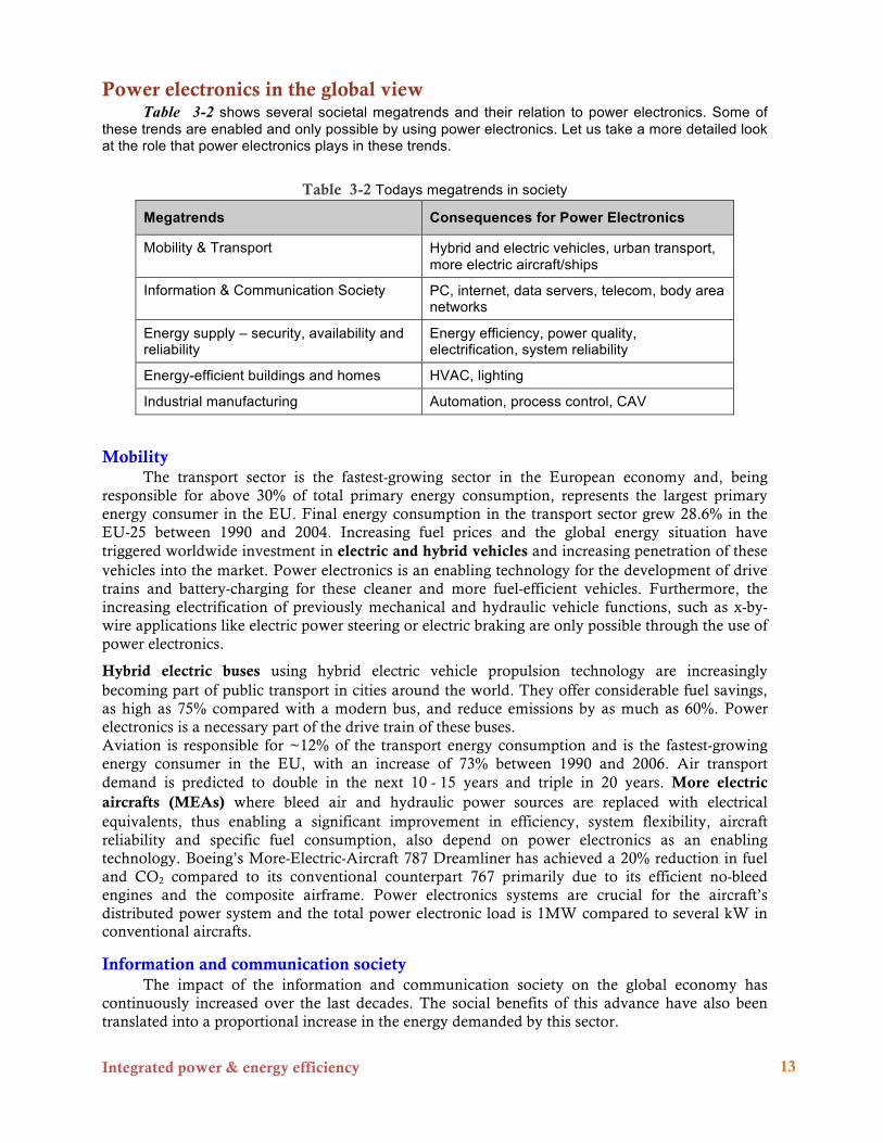
Power electronics in the global view Table 3-2 shows several societal megatrends and their relation to power electronics. Some of
these trends are enabled and only possible by using power electronics. Let us take a more detailed look at the role that power electronics plays in these trends.
Table 3-2 Todays megatrends in society
Megatrends Consequences for Power Electronics
Mobility & Transport Hybrid and electric vehicles, urban transport, more electric aircraft/ships
Information & Communication Society PC, internet, data servers, telecom, body area networks
Energy supply – security, availability and reliability
Energy efficiency, power quality, electrification, system reliability
Energy-efficient buildings and homes HVAC, lighting
Industrial manufacturing Automation, process control, CAV
Mobility The transport sector is the fastest-growing sector in the European economy and, being
responsible for above 30% of total primary energy consumption, represents the largest primary energy consumer in the EU. Final energy consumption in the transport sector grew 28.6% in the EU-25 between 1990 and 2004. Increasing fuel prices and the global energy situation have triggered worldwide investment in electric and hybrid vehicles and increasing penetration of these vehicles into the market. Power electronics is an enabling technology for the development of drive trains and battery-charging for these cleaner and more fuel-efficient vehicles. Furthermore, the increasing electrification of previously mechanical and hydraulic vehicle functions, such as x-by-wire applications like electric power steering or electric braking are only possible through the use of power electronics.
Hybrid electric buses using hybrid electric vehicle propulsion technology are increasingly becoming part of public transport in cities around the world. They offer considerable fuel savings, as high as 75% compared with a modern bus, and reduce emissions by as much as 60%. Power electronics is a necessary part of the drive train of these buses. Aviation is responsible for ~12% of the transport energy consumption and is the fastest-growing energy consumer in the EU, with an increase of 73% between 1990 and 2006. Air transport demand is predicted to double in the next 10 - 15 years and triple in 20 years. More electric aircrafts (MEAs) where bleed air and hydraulic power sources are replaced with electrical equivalents, thus enabling a significant improvement in efficiency, system flexibility, aircraft reliability and specific fuel consumption, also depend on power electronics as an enabling technology. Boeing’s More-Electric-Aircraft 787 Dreamliner has achieved a 20% reduction in fuel and CO2 compared to its conventional counterpart 767 primarily due to its efficient no-bleed engines and the composite airframe. Power electronics systems are crucial for the aircraft’s distributed power system and the total power electronic load is 1MW compared to several kW in conventional aircrafts.
Information and communication society The impact of the information and communication society on the global economy has
continuously increased over the last decades. The social benefits of this advance have also been translated into a proportional increase in the energy demanded by this sector.

Integrated power & energy efficiency
14
In Western Europe the demand for IT services was about 60 TWh of electricity consumption (with another 20 TWh in the residential sector) and it is expected to rise to 104 TWh per year by 2020. In 2006, the power use associated with servers and data centers, including storage and network equipment, was about 1.5% of total US electricity consumption, and it is projected to increase to 2.5% of total electricity consumption by 2011. The peak load consumption of US data centers is around 8 GW, equivalent to 16 base-load power plants. The use of advanced power electronics techniques, like new DC distribution networks, can lead to a 10% reduction of the required energy. The integration of ICT technologies and power electronics, improving energy management, can yield an additional 20% energy saving, and the implementation of best practices can lead to a 50% reduction.
Today microprocessor industry is not only focused on the performance per euro but also on the performance per watt. Load consumption can be dramatically reduced by appropriate power supply strategy. Techniques like Dynamic Voltage Scaling that adjust the supply voltage of the microprocessor as a function of the work load can achieve significant reduction on the consumed power. Further improvements can be achieved increasing the efficiency of the power converters under light load conditions (e.g. when the processor is in idle mode) by means of reconfigurable power stage as a function of the load, adjustable digital control and optimization of dead times.
The annual electricity consumption related to standby functionalities and off-mode losses in the EU was estimated to be 47 TWh in 2005. Without taking specific measures, the consumption is predicted to increase to 49 TWh in 2020. An important portion of these losses is related to power supplies hence novel power electronics techniques for achieving high efficiencies at low loads are necessary. Further savings can be expected from the application of efficient power supplies in electronics appliances, such as TVs, VCRs, microwave ovens, etc.
It is estimated that European consumption of broadband equipment will be up to 50 TWh per year by 2015. Power amplifiers are one of the main building blocks of all modern wireless communications systems. They are used in all base stations and all the mobile units which are currently available. To maintain the required levels of system performance current commercially available amplifiers are designed to operate with extremely poor levels of efficiency, which means they consume far more energy than is strictly necessary. Power electronics techniques are also here crucial for reducing the energy consumption.
Energy supply – security, availability and reliability The increasing energy demand, the shortage and finiteness of fossil fuels and the need for
carbon footprint reduction in order to prevent hazardous climate changes have brought the issue of energy into the spotlight of political and public attention. Electrical energy is one of the cleanest, most efficient and versatile forms of energy and it is predicted that its demand will continue to grow at a much faster rate than other energy sources in the coming decades. In recent years there has been a growing awareness within the electricity supply industry of the need to reinvent Europe’s electricity networks in order to meet the demands of twenty-first-century customers. In 2005 the European SmartGrids Technology Platform was established as a coherent approach to meet the challenges envisaged by network owners, operators and particularly users, across the EU. In the EC paper “Vision and Strategy for Europe’s Electricity” it was concluded that future electricity markets and networks must provide all consumers with a highly reliable, flexible, accessible and cost-effective power supply, fully exploiting the use of both large centralised generators and smaller distributed power sources across Europe. End users will become significantly more interactive with both markets and grids; electricity will be generated by centralised and dispersed sources; and grid systems will become more inter-operable at a European level to enhance security and cost-effectiveness. This new concept of electricity networks is described as the ‘SmartGrids’ vision.

Integrated power & energy efficiency
15
One of the priority actions of the EC Action Plan for Energy Efficiency is to make power generation and distribution more efficient. Transmission and distribution (T&D) losses of electrical energy are typically between 6% and 8%. Business Roundtable’s Energy Task Force T&D Working Group, which ABB chairs, identified a number of energy-efficient technologies for grids, including power electronics technologies such as HVDC, FACTS, power electronic transformers, distributed generation/microgrids (power electronics is necessary to interface distributed generators such as wind turbines, solar cells etc. to the grid) etc. Power electronics has been identifies as a key technology in all four pillars of Smart Grids:
• Integration of renewables (wind turbine converters, HVDC for offshore wind park connection, SVC/STATCOM for grid code compliance, energy storage for improving stability and decreasing power fluctuations, solar converters etc.)
• Integration of electric vehicles ((fast) charging of electric vehicles, traction drive for hybrid (electric) vehicles, dynamic energy storage to absorb peaks due to simultaneous (fast) charging of electric vehicles)
• Reliability and efficiency (efficient long distance transmission with HVDC, variable speed drives in industrial plants and pumped hydro stations, energy storage for emergency and peak power, power quality solutions for industry etc.)
• Demand response (converter interface to distributed generation with built-in load management capability, drives in pumped hydro station with remote control from control centre).
Sustainable buildings and homes Energy use in residential and commercial buildings is responsible for about 40% of the EU's
total final energy consumption and CO2 emissions of which more than 50% is electrical energy. The cost-effective energy-saving potential by 2020 is significant: 30% less energy use within the sector is feasible. This equals a reduction of 11% of the EU's final energy use. The sector has significant untapped potential for cost-effective energy savings which, if realised, would mean an 11% reduction in total energy consumption in the EU by 2020.
Smart Homes, also known as automated homes, intelligent buildings, integrated home systems or domotics, have been gaining in popularity in the past few years. Smart homes incorporate common devices that control features of the home. Originally, smart home technology was used to control environmental systems such as lighting and heating, but recently the use of smart technology has developed so that almost any electrical component within the house can be included in the system. A reliable source of energy is mandatory for all these developments. Home energy management relying on power electronic systems is therefore one of the key issues for home automation. Such a distributed energy management would also interface the local renewable energy sources such as solar panels and the home loads.
Energy-positive buildings are those that generate more power than their needs. They include the management of local energy sources (mainly renewable, e.g. solar, fuel cells, micro-turbines) and the connection to the power grid in order to sell energy if there is excess or, conversely, to buy energy when their own is not sufficient. They use systems and components such as advanced Heating, Ventilating and Airconditioning (HVAC) and highly efficient lighting. They are equipped with intuitive devices that not only meter the energy consumed but also provide real-time information (e.g. on incentive pricing, deviations from standard consumption) to help people living in (or managing) these environments save energy while maintaining the desired comfort levels. They include Plug-in Electric Vehicles infrastructures in order to facilitate not only clean transport but also alternative local energy storage.
Lighting consumes more than 20% of all electricity generated in the European Union (EU). The situation is similar in the United States and the percentage is even higher in some developing
Integrated power & energy efficiency
16
countries, since lighting is one of the largest uses of electric power. Power electronics is an enabling technology for new energy efficient lighting technologies. Gas discharge lamps such as fluorescent and HID lamps cannot be operated directly from the mains, because they have negative incremental impedance, and therefore, must be operated in series with current controlled ballast. To improve the efficiency of gas discharge lamps, the traditional magnetic ballasts can be replaced by high-efficiency electronic ballasts. The use of high-frequency electronic ballasts results in significant ballast volume and weight reduction and improves the performance of the discharge lamp. The high-frequency operation also makes the lamp start easily and reliably, and eliminates audible noise and flickering effects. In addition, due to the advances in power electronics, power regulation can be easily incorporated into the ballast, making intelligent energy management feasible. LED technologies and in some case plasma technology is being used for both indoor and outdoor next generation high efficiency lighting solutions and power electronics is playing a key role in developing high efficiency drivers for optimising their operation.
Industrial manufacturing Nearly one-third of the world’s energy consumption and 36% of its carbon dioxide (CO2)
emissions are attributable to manufacturing industries. Manufacturing is still the driving force of the European economy, contributing over 6.500 billion euro in GDP. It covers more than 25 different industrial sectors, largely dominated by SMEs. There is an increasing demand for greener, more customised and higher quality products. The European manufacturing sector faces an intense and growing competitive pressure in global markets. European companies are faced with continuous competition in the high-tech sectors from other developed economies, such as the U.S, Japan and Korea. Manufacturing has to address the challenge of producing more products with less material, less energy and less waste. Together with other industrial technologies, ICT and advanced materials, power electronics-enabled variable-speed control of motors as an enabler for higher automation and better process control will improve the competitiveness of the companies. Power electronics in combination with wireless sensor technology can also be utilised for machine conditional monitoring applications, checking that electrical machines are operating in accordance with expected efficiency norms as well as enabling predictive maintenance to ensure machines are repaired/maintained in advance of breakdown thereby minimising downtime and associated losses.
Conclusions Power electronics is a key technology for the efficient conversion, control and conditioning of electric energy from the source to the load. The energy saving potential of power electronics in various applications is related to highly efficient variable speed motor drives with energy recovery, to smart power supplies enabling high efficiency over a wide load range and zero-power standby function as well as to energy efficient and low-emission mobility with hybrid and full electric vehicles. Furthermore, power electronics is enabling a sustainable energy supply based on renewables by feeding-in wind and solar power efficiently to the electricity grid and by stabilizing the grids while the share of fluctuating renewables is increasing. The estimated energy savings potential that can be achieved by introducing power electronics into systems is enormous, more than 25% of the current EU-25 electricity consumption. References [E4U2009] Public Final Report of the E4U Project ´Electronics enabling efficient energy usage´
funded by the European Commission´s ICT programme in FP7 (project no. 224161), 2009 [Popovic2012] J. Popovic-Gerber et al ´Power electronics enabling efficient energy usage: energy
savings potential and technological challenges´ IEEE Transactions on Power Electronics, vol. 27, no. 5, pp. 2338-2353, May 2012

Integrated power & energy efficiency
17
4. Section 2: Power devices
Figure of merit and Benchmarking Power- Si – SiC – GaN
Steve Stoffels (IMEC) With the contribution of:
Anton Bauer (Fraunhofer IISB) Jürgen Lorenz (Fraunhofer IISB) Leo Lorenz (ECPE) Angelo Magrì (STMicroelectronics) Peter Moens (ONsemiconductor) Joachim Pelka, (Fraunhofer VµE) Jan Sonsky (NXP) Renaud Stevens (SOITEC)
Abstract
This section will describe the figures of merit and perform a benchmarking of several technologies and devices to each other. This benchmarking will be split in three different ranges which target different market segments, namely low voltage devices (for e.g. switched mode power supplies), medium voltage devices (for motor control and heavy duty appliances) and the high voltage range (energy transmission and distribution).
The section is split in three different subsections. The first subsection will identify and describe important electrical parameters, which are commonly used to characterize power transistors. These parameters are breakdown voltage, leakage (gate and drain), on-resistance, threshold voltage, input-output and transfer capacitance and the gate charge (with gate-source and gate drain components. The second subsection will look into more detail at several key figures of merit. These figures of merit relate several material properties and/or electrical characteristics to each other in such a way that the value of the FOM can act as a metric for comparing different devices or technologies to each other. The significance and meaning of each figure of merit will be explained and the analytical formula’s used for calculating their values will be shown. The figures of merit that will be described are the conduction losses, on-state losses, specific on-resistance, Johnson figure of merit, Keyes figure of merit, Baliga’s figure of merit and Baliga’s high frequency figure of merit.
In the last subsection the datasheets for of several selected power semiconductor components will be shown. Components will be selected for each of the device technologies under investigation in this document, namely Silicon, SiC and GaN. Furthermore, different device architectures (e.g. unipolar versus bipolar) will also be compared. To leverage the strengths of each device architecture and technology, the subsection will be split in a low-voltage, medium voltage and high voltage category. In this way the proper device architecture can be chose for the specific category and compared to relevant device from other material systems. The figures of merit will also be calculated and plotted on a graph, together with the intrinsic material dictated limits for each technology.

Integrated power & energy efficiency
18
Electrical parameters In a standard datasheet one can find many electrical parameters related to the electrical and
thermal performance of the component. To be able to compare and benchmark different components, it is necessary to understand the meaning of these parameters and how they relate to device performance and operation. An example of such a datasheet for a typical MOS transistor is shown below (Figure 4-1):
Figure 4-1 Example of a datasheet for a silicon POWERMOS datasheet (Fairchild
FDMS039N08B).
Integrated power & energy efficiency
19
The most important electrical parameters in the datasheet and their significance are described in the rest of this section.
Breakdown voltage (BVds): is the drain-source voltage at which no more than the specified drain current will flow at the specified temperature and with zero gate-source voltage (in the case of normally OFF devices). In high-voltage Silicon devices, BVds is normally defined by the avalanche process whereas in WBG devices other phenomena could be relevant. BVds is typically defined above the nominal voltage of the application in order to accommodate parameter dispersion and overvoltage. In the application, voltage overshoots exceeding BVds could result in reliability issues as well as self-damping effect.
Drain-source leakage (Idss): is the drain-source leakage current at a specified drain-source voltage when the gate-source voltage is zero voltage (in the case of normally OFF devices).. Although Idss increases with temperature, the off-state power loss is Idss times drain-source voltage and it is usually negligible.
Gate reverse leakage (Igss): is the leakage current that flows through the gate terminal at a specified gate-source voltage. Igss is normally negligible with respect to the current supplied to charge or discharge the gate thus having no influence on the system losses.
On-resistance (Rds,on): is the drain-source resistance at a specified drain current and gate-source voltage. Rds,on governs the power switch conduction losses, which are calculated by Rds,on times the drain current square.
Threshold voltage (Vth): is the gate-source voltage above which drain current becomes relevant. In the application, the driving voltages and gating energies are reduced with Vth.
Input capacitance (Ciss): is the capacitance measured between the gate and source terminals for AC signals (drain shorted to source). Ciss is constituted by the gate to drain capacitance Cgd in parallel with the gate to source capacitance Cgs. Ciss must be charged to the threshold voltage before the device begins to turn on, and discharged to the plateau voltage before the device turns off. Therefore, Ciss has a direct effect on the turn on and turn off delays.
Output capacitance (Coss): is the capacitance measured between the drain and source terminals for AC voltages (gate shorted to source). Coss is constituted by the drain to source capacitance Cds in parallel with the gate to drain capacitance Cgd. Coss affects the dV/dt and the resonance of the circuit during transient times.
Reverse transfer capacitance (Crss): is the capacitance measured between the drain and gate terminals for AC voltages (source connected to ground), often referred to as the Miller capacitance. Crss is equal to the gate to drain capacitance. Crss is one of the major parameters affecting voltage rise and fall times during switching.
Gate-source charge (Qgs): is the charge related to the gate-source capacitance. Besides its important contribution to the total Qg, Qgs plays an important role in preventing spurious turn-on events in the application.
Gate-drain charge (Qgd): is the charge related to the Miller capacitance and depends on drain-source voltage. It is also a parameter that influences switching characteristics.
Gate charge (Qg): is the total gate charge, made up by Qgs, Qgd and the “overdrive charge” after charging the Miller capacitance. This is the characteristic parameter that determines gate peak current for driving the gate and drive loss.

Integrated power & energy efficiency
20
Power transistor figures of merit In this section several key figures of merit will be introduced, which will allow one to
evaluate the performance of several different components and technologies, with respect to each other. We will mainly focus on the efficiency as a metric to compare the performance of different power components.
Efficiency: Power convertor circuits are not ideal, therefore part of the energy that is switched or converted will be lost either as heat or another form of energy. The efficiency is a value defining how “good” a circuit is in converting electrical energy. Efficiency should be as high as possible to reduce the amount of losses. A large part of these losses are generated in the power switching component. The understanding and minimization of these losses on component level is required to further improve performance of power electronics.
The power losses for a semiconductor power component are given by the following relation [Nakagawa2006]: 𝑃!"## = 𝑅!"(!")𝐼!,!"#! + 𝐼!𝑉!
𝑄!"𝐼!
𝑓 +13𝑄!"𝑉!𝑓 (1)
Where Rds(on) is the on-resistance, ID is the current through the transistor in the on-state, ID,rms the root mean square value of ID, VD is the voltage over the transistor in off-state, Ig is the current applied at the gate, Qsw is the total charge injected at the gate during switching, f is the switching frequency and Qds is the charge related to the junction capacitance between source and drain.
In eqn (1) there are several loss mechanisms present; the first term on the right hand side represents the on-state losses. These are joule losses because of the resistance of the transistor when in the on-state. The second and third terms are the switching losses and the junction capacitance losses [Nakagawa2006], which are caused by stored charges in the component. Usually the junction capacitance losses are neglected and one focuses on the on-state and switching losses for power switching components.
The conduction losses and switching losses scale differently with the area, leading to a tradeoff in die-size when minimizing the losses, see Figure 4-2.
Figure 4-2 Tradeoff between conduction (on-state) losses and switching losses versus the device active area. Shown for a 30V, 500A MOSFET structure [Baliga2008].

Integrated power & energy efficiency
21
The minimum power loss can be calculated by summing the conduction and switching losses and finding the point at which dP!"##/dA = 0, leading to a value of:
P!"##,!"# = 2I!,!"#
V!I!fi!
R!"(!") ⋅ Q!",!"
The first term in the minimum losses (Ploss,min) is related to the operation of the circuit, while the second parameter is determined by technology, therefore a figure of merit for switching losses can be derived [Huang2004]:
FOM = R!" ⋅ Q!"
In the literature Qsw is often taken to be the total gate charge Qg leading to the often seen figure of merit:
HFOM = R!" ⋅ Q!
This is the most important Figure of merit when comparing different technologies to each other. There are several other figures of merit, which are often used to evaluate the effectiveness of different material as a base for a power technology. Such examples are the Baliga Figure of merits and Johnson figure of merit [Baliga1989, Johnson1965]
Benchmarking Semiconductor switches are not ideal; therefore not all switches can be used in all type of
applications. It is therefore necessary to make a distinction between different applications and have a critical look at the power rating for these applications, i.e. the voltage/current handling ability and switching speed.
There is a wide range of voltages over which power conversion should operate, this ranges from several volts (V) to tens of kilovolts (kV). There are three big classes into which power semiconductors are classified, namely low voltage, medium voltage and high voltage applications [Rohm2011].
1. Low voltage (several volt-600V): The low voltages are the least demanding and usually require low cost combined with compact sizes, voltages range from several volts to several hundred volt and the main applications are consumer gadgets, IT power supplies and lighting.
2. Medium voltage (600V-1.2kV): In the medium range there are applications, which are of interest in the field of renewables and sustainable energy, namely electrical drivetrains for cars, solar panel convertors, motor drives and robotics.
3. High voltage (2kV-10’s of kV): This range is dominated by electrical power transmission and drives for electrical trains.
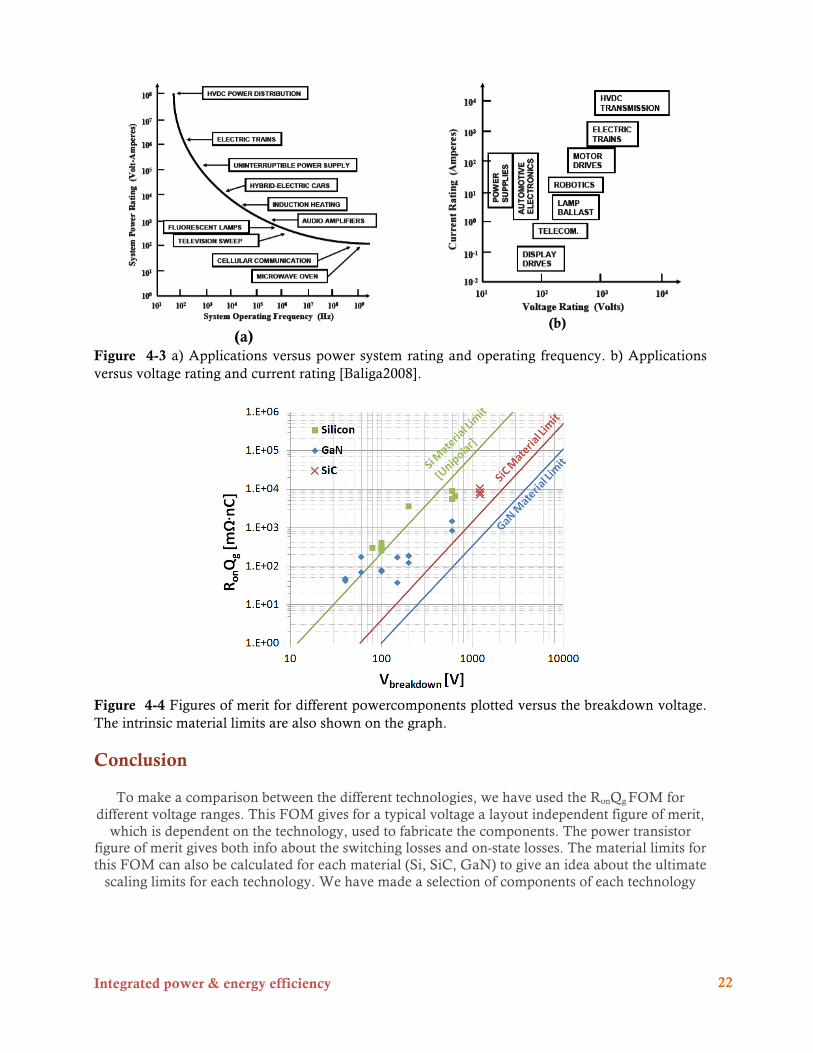
Integrated power & energy efficiency
22
(a)
(b)
Figure 4-3 a) Applications versus power system rating and operating frequency. b) Applications versus voltage rating and current rating [Baliga2008].
Figure 4-4 Figures of merit for different powercomponents plotted versus the breakdown voltage. The intrinsic material limits are also shown on the graph.
Conclusion
To make a comparison between the different technologies, we have used the RonQg FOM for different voltage ranges. This FOM gives for a typical voltage a layout independent figure of merit,
which is dependent on the technology, used to fabricate the components. The power transistor figure of merit gives both info about the switching losses and on-state losses. The material limits for this FOM can also be calculated for each material (Si, SiC, GaN) to give an idea about the ultimate
scaling limits for each technology. We have made a selection of components of each technology

Integrated power & energy efficiency
23
and calculated the FOMs, the components are listed in
Table 4-1. We also plotted the calculated figures of merit, together with the material limits in Figure 4-4. It can clearly be seen that both GaN and SiC already exhibit Figures of Merit, which are currently about a factor 5 better than what can be achieved with silicon technologies. Currently the biggest improvements for GaN can be seen for the medium voltage range (200-600V). For the low voltage applications (60V-200V), the figures of merit for GaN are slightly better than what is achievable with silicon, however they are not yet under the material limit of silicon. There is still much room for improvement in the low voltage range by further optimizing the contact resistance in the component. SiC components currently only exist for high voltage applications (1200V), the FOM is an order of magnitude better than silicon FOM’s. It is harder however for SiC to compote in the medium-low voltage ranges due to the high price of the components. In general all of the FOM’s for the wide bandgap (WBG) power components are still orders of magnitude above the material limit, so there is still much headroom to improve the performance of these components.

Integrated power & energy efficiency
24
Table 4-1 Characteristics and FOM for selected GaN/SiC/Si power components
In this section the most important figure of merit for switching power component was calculated for the latest generation of power components on the market, and this for different competing technologies. It was shown that the FOM for silicon technologies are close to material dictated limits and it will be hard and expensive to get further incremental improvements in performance. GaN and SiC on the other hand are disruptive technologies that offer orders of magnitude better FOM’s than silicon. First generation products already show figures of merit, which are a factor 4 to 5 better than the latest generation of silicon technologies, with much headroom for future improvements. For GaN the biggest gain for the FOM is currently achieved in the medium voltage range (200V-600V), while for the low voltage range the contact resistance needs to come down further and currently puts a limit on the low voltage FOM. SiC on the other hand is currently only available for the higher end of the medium voltage range (1200V), due to its high cost which makes it difficult to compete in the lower voltage ranges. Investment in GaN should focus on optimizing in advantage in the medium power range and driving the cost of the products down to compete more easily in this market. Home appliances and consumer electronics are a huge potential market with applications in this voltage range. At the same time effort should

Integrated power & energy efficiency
25
be spend on lowering the contact resistances in the GaN material to allow penetration of the technology in the lower voltage ranges, where there is a huge market for switched mode power supplies for IT and servers. SiC should leverage its strength at the high voltage ranges. Breakdown voltages and on-state voltage drops are unmatched for vertical SiC devices. Power transmission and large electrical engines such as locomotives should be a potential market and funding should focus on developing SiC technology to displace established IGBT’s and Thyristors in this voltage range. In the literature, bipolar SiC transistors have been shown to operate at breakdown voltages between 10.000-20.000V. Such high breakdown voltages translate in a drastic reduction of the amount of components needed to handle the very large voltages for electric power distribution, which can be in excess of 100kV. At the same time SiC will offer in these voltage ranges improved figures of merit, with respect to silicon, leading to a reduction of losses. SiC should therefore be an enabler for an efficient smart grid of the future. In the higher regions of the medium voltage range (target application = automotive), there will be an intense competition between GaN and SiC. GaN holds the price advantage and prospect of improved figure of merit, but currently lacks a stable and reliable device at these breakdown voltages. The potential for the technology to operate in this field is there, therefore strategic investments should be necessary to further develop the technology for this application domain (increase breakdown voltage, avalanche rating of components and addressing dispersion are key challenges). SiC already exhibits voltages in the range needed for automotive (1200V), but reliability concerns should be addressed.
References [Baliga1989] Power Semiconductor Device Figure of Merit for High-Frequency Applications. Baliga, B. J.
October 1989, IEEE Electron Device Letters, Vol. 10, pp. 455-457. [Baliga2008] Baliga, B. Jayant. Fundamentals of Power Semiconductor Devices . s.l. : Springer, 2008.
ISBN:978-0-387-47313-0. [Huang2004] New Unipolar Switching Power Device Figures of Merit. Huang, Alex Q. 5, May 2004,
IEEE Electron device Letters, Vol. 25, pp. 298-301. [Johnson1965] Physical limitations on frequency and power parameters of transistors. Johnson,
E. O. 1965, RCA Rev., pp. 163-177. [Nakagawa2006] Evolution of silicon power devices and challenges to material limit. Nakagawa, Akio.
2006. International Conference on Microelectronics. pp. 158-165. [Rohm2011] Rohm semiconductors. [Online] [Cited: 05 01, 2011.]
http://www.rohm.com/products/sic/dmos.html.

Integrated power & energy efficiency
26
Si –Power devices
Sonsky Jan (NXP Belgium) With the contribution of:
Magrì Angelo (STMicroelectronics) Peter Moens (ON-Semiconductor) Wolfgang Dettmann (Infineon) Pelka, Joachim (Fraunhofer) Jürgen Lorenz (IISB) Leo Lorenz (ECPE)
Abstract Si power devices have evolved over last several decades and dedicated device structures were
engineered for different voltage classes. Along the way, numerous innovations have been realized to improve different aspects of device performance often beyond the so-called silicon-material-limits. This chapter will start with discussion of key differences between discrete and integrated power devices and the following sub-sections will zoom-in to different available discrete technologies, including Low Voltage MOSFETs, High Voltage MOSFETs and IGBTs.
Each section will cover key device types and innovation trends, including comparative performance assessment of the different competing components. Secondly the essential manufacturing technologies required to produce the different components will be discussed. Thirdly typical failure modes and reliability aspects specific to each technology type will be addressed. Finally fundamental performance limitations will be outlined. This will provide a good link to the other parts of the report discussing potential of wideband-gap based power components. As the device scaling (and hence power density increase) continues, higher switching frequency is utilized and operating temperature increases, one of the innovation trends is towards so-called “smart discrete”. These are components with on-chip integrated self-protection components. Finally this part of the report will conclude with mapping the different power components and technologies on applications and circuit topologies.
Discrete vs. Integrated Power Devices The power device implementations and solutions have branched out to several distinct paths
already several decades ago. Power devices integrated in CMOS technologies alongside logic and analog circuit blocks are typically used in different power management ICs, display drivers or automotive networking ICs. Integrated power follows mainstream CMOS roadmap with about 2 to 5 years delay (see Figure 4-5). Low-voltage (below 50V) components are usually realized using Lateral DMOS (LDMOS) devices with different type of substrate isolation depending on robustness requirements, from implanted wells to buried epitaxy layers to SOI isolation. Device components aiming at higher voltage (50V up to several 100s V) or higher robustness are usually implemented as Vertical DMOS with deep & heavily doped buried region used as drain terminal. The drain is eventually connected upwards using implanted or trench-based link.
Discrete power devices are mostly vertical. Low Voltage (LV, below 100V) have usually both drift region as well as channel region vertical to maximize area efficiency and reduce total specific RON. Since on-resistance of high voltage (HV, above 600V) is determined by 90% or more by drift

Integrated power & energy efficiency
27
region resistance, HV components are VDMOS-type with channel region located on top-surface. HV components for high-current applications (above 20A) are predominately based on insulated-gate bipolar (IGBT) technology. Examples of different device solutions are shown in Figure 4-6 and will be discussed in more details in following sub-sections.
Figure 4-5 Integrated Power vs. mainstream CMOS roadmap.
(a)
(c)
(b)
Figure 4-6 Typical device architectures: (a) lateral DMOS, (b) integrated vertical DMOS, (c)
discrete vertical DMOS.

Integrated power & energy efficiency
28
Low Voltage MOSFETs Since the introduction of the discrete vertical DMOS introduced by International Rectifier in
the early 1980s, the performance of power MOSFETs has significantly improved aided by the introduction of more complex device structures and the use of advanced techniques such as RESURF and superjunctions. This is demonstrated in Figure 4-7, which shows the improvement over time of the on resistance (RDS(on)) and gate charge for a 30V power MOSFET in an SO8 footprint.
Figure 4-7 Lowest RDS(on) available from NXP Semiconductors in an SO8
In power ICs, lateral device structures (Figure 4-8 a), are commonly employed using
extended drain and RESURF concepts. The advantage of this type of structure is that it is easily integrated with control circuitry on a single die and is common in low power applications. However, due to the high mask count and high RDS(on) per unit area of this type of structure, discrete vertical devices are more cost effective at higher power levels. A critical factor in determining the RDS(on) of a device is the physical size (cell pitch) of the structure. Lateral devices need to include the drift region of the devices within the cell pitch (i.e. in the lateral direction). The drift region is the part of the device that is used to withstand the voltage rating of the MOSFET and increases in length as the voltage rating of the MOSFET increases. This ultimately limits the reduction in device size/cell pitch as process technology improves (i.e. it prevents lateral power devices following the reductions in size achieved in CMOS technologies). To overcome this limitation the vertical DMOS structure was introduced in the early 1980’s (Figure 4-8b), in this device the channel (the actual MOSFET switch) is on the surface and conduction through the channel is lateral but the drift region of the structure is incorporated vertically and thus no longer

Integrated power & energy efficiency
29
restricts reduction in device size; there are also now two channels created within the cell pitch. From 1995 onwards, the trench structure, introduced by Siliconix, replaced the vertical DMOS structure for voltages below 100V. The trench structure (Figure 4-8c) allowed for a further reduction in device size by making a true vertical device where both the channel and drift region are vertical.
A disadvantage of the trench structure, which achieves a low RDS(on) by having allowing for a small cell pitches (<1µm is common), is that the gate charge is high. This is due to the additional gate drain capacitance at the bottom of the trench, which is not present in lateral structures. This high gate charge, lead to further evolutions in the trench structure, initially by using a thick oxide at the bottom of the trench (≈2004, Figure 4-8d) and by employing the more complex split gate structure (Figure 4-8e). This structure first demonstrated by NXP in 2007 and available commercially from around 2008 is now the industry standard structure for low voltage MOSFETs. Whilst trench based structures allow for a small cell pitch, it does not significantly impact the resistance of the drift region, which becomes of increasing importance above 40V. To address this issue, the design of trench based technologies have been supplemented by applying the RESURF (or charge balance) principle. This can be achieved either by using the superjunction approach commonly used for 600V power MOSFETs (Figure 4-8f) or using field plates (Figure 4-8g), which is easily combined with the split gate approach (Figure 4-8e).
However, the pursuit of low RDS(on) is not always beneficial as it can result in poor switching performance and low efficiency in fast switching circuits. This has lead to the introduction by TI of a pseudo lateral structures (Figure 4-8h) based on RF LDMOS technology, which provides a level of performance only matched by the most advanced Trench technologies as shown in Figure 4-9. High cell densities are also detrimental in applications where the power MOSFET is used to control the current (e.g. motor control, inrush current limiting). In these applications modern devices are prone to thermal runaway. In these cases either vertical DMOS or wide cell pitch trench technologies are preferred.
With the low channel and drift resistances afforded by modern devices approaching theoretical limits, package and substrate resistance also are being improved. The use of copper clip interconnects are now standard for low RDS(on) devices. At voltages ≤30V the substrate can contribute up to a third of the total resistance, which has lead to a drive ever decreasing wafer thickness with the trend to 50µm thick wafers. A survey of the lowest RDS(on) as a function of voltage rating and manufactures in an SO8 footprint is shown in Figure 4-10.
Modern power MOSFETs are extremely robust with respect to voltage overshoot, where early devices could fail catastrophically when taken into avalanche, the use of high cell densities and trench structures mean that the parasitic npn bipolar, the cause of failure during avalanche, is shorted out. Current focus on the reliability of power MOSFETs is on the screening out of manufacturing defects especially in the Automotive market where zero defect programs are implemented. In this instance the high ruggedness capability of these devices allows high current avalanche screening tests to be used to remove defective products
The most common technology node to create low voltage power devices is 0.35µm, which is commonly available in depreciated foundry fabs with a trend towards 0.18µm at ≤40V where submicron cell pitches are common. Production is largely on 200mm and 150mm wafers with at least one manufacturer developing production on 300mm.

Integrated power & energy efficiency
30
(a) (b) (c)
(d) (e) (f)
(g)
(h)
Figure 4-8. Power MOSFET structures: (a) Lateral MOSFET, (b) Vertical DMOS; (c) Trench, (d) Thick bottom oxide trench, (e) split-poly (charge balanced) trench, (f) superjunction trench, (g) Charge balanced trench,.(h) Pseudo-Lateral MOSFET
N- N+N+
PP
GS D G
S
D
S
G
D
N+ N+
P
N
G
D
S
S S
SG
D
S

Integrated power & energy efficiency
31
Figure 4-9 Comparison of Gate Charge vs. RDS(on) of three Trench technologies and a Pseudo
lateral structure optimised for low gate charge.
Figure 4-10 Survey of lowest RDS(on) MOSFET available in a power SO8 footprint as a function of
voltage rating
High Voltage MOSFETs A traditional HV MOSFET (Figure 4-11) has high voltage off-state capability determined by
n-epitaxy thickness and doping. The triangular electrical field profile leads to poor scaling of on-resistance with BVds. In 600V-rated MOSFETs, Ron due to epitaxy is typically 90% or more of the total device resistance. Invention of superjunction led to brekthrough in HV MOSFET performance. Superjunctions are based on alternating n- and p-type regions in the drift regions. These regions are designed so that the charges in the p- & n-regions are in exact balance. This leads to an enhanced depletion alongside the additional p/n junction leading to rectangular electrical

Integrated power & energy efficiency
32
field profile in the drift region and hence much better scalling of BVds with epitaxy thickness. The increased doping in the electron-conducting n-regions results in lower Ron.
Figure 4-11 High Voltage Vertical DMOS with different on-resistance contributions.
The main challenge in manufacturing superjunction MOSFETs is to ensure sufficient
process robustness against variation of the charge balance in the n- and p-type regions. Different practiced approaches are summarizied in Figure 4-12. The first approach pioneered by Infineon is based on multiple epitaxy growth (n-type region) with multiple p-type doping (p-type regions). The doping control (and hence charge balance) can be controlled within 2-3% for n-epitaxy regions and about 1% for the p-doped regions. This method is relatively costly as it requires repeating the process sequence several times to realize structure supporting 600V or higher voltage. It is also believed that the pitch of n-type and p-type regions is limited due to the outdiffusion of p-type doped regions during the subsequent epitaxy growth.
To address these limitations, alternative approach is based on etching very deep trenches (throughout the HV epitaxy thickness) and refilling the complete trench with p-type epitaxy to realize the p-doped regions. Since doping in both n-/p-regions is defined by epitaxy, the charge control is limited to about 2-3% in each region. Given the advances in deep-trench etching, it is believed that this approach has better pitch scalability. The main challenge is realizing defect and void free epitaxy in such highly non-conformal structure.
Alternative approach also utilizes deep-trenches, but the p-type regions are only formed on the trench sidewall using Boron drive from plasma (vapor phase doping). The trenches are then partly or completely filled with a dielectric. The charge control is similar to epitaxy-based solutions, while the complex epitaxy is no longer required. The main challenge is dielectri-filling of the deep trenches and related build-in stress.
Yet another approach is based on realizing the n- and p-type regions on the sidewall of deep trench using a dual-epitaxy. The trench is then refilled with a dielectric or a dielectric plug is used at the top of the trench leaving void behind.

Integrated power & energy efficiency
33
(a)
(b)
(c)
(d)
Figure 4-12 Different types of superjunction HV-MOSFETs: (a) multiple-epitaxy & multiple-implant, e.g. CoolMOS by Infineon, (b) deep trench etch and epitaxy refill (e.g. Fairchild), (c) deep
trench etch with sidewall p-type doping and dielectric refill (e.g. NXP) and (d) deep-trench etch with dual n/p-type epitaxy refill (e.g. ON-Semi).
Figure 4-13 Specific Ron roadmap of superjunction VDMOS transistor by different semiconductor makers. Data are for 600V, unless mentioned otherwise.

Integrated power & energy efficiency
34
On-resistance evolution of the different 600V superjunction MOSFETs is shown Figure 4-13. The on-going R&D activities on superjunction devices are mainly focused on
• Further reduction of specific on-resistance
• Realizing and improving Ron of 900V rated MOSFETs
• Improving avalanche ruggedness
• Reducing Eoss and Qoss (i.e. energy and charge stored in output capacitance) to improve efficiency of hard-switching circuits
Reducing Qg and Rg to enable higher switching frequency operation
IGBTs In many fields of application, ranging from industrial to consumer electronics, need for
power has increased dramatically in the last years. The insulated Gate Bipolar Transistor (IGBT) plays a key role in mid/high power range, having both the advantages of bipolar conduction and insulated-gate voltage control that means both low on-state voltage drop and low switching losses. Thanks to these peculiarities, big efforts have been conducted to improve the IGBT technology.
In about twenty years we have experienced many generations of planar technologies in which the device elementary cell shrinking allowed a higher channel density in order to improve the forward conduction performances.
After, we have experienced the success of trench-gate IGBT. This structure allows a much higher channel density, leading to a lower channel resistance than planar devices. Furthermore, the parasitic JFET effect is completely eliminated in the trench structure, thus further reducing the forward voltage drop.
Having reached the limit in terms of performances regarding the top structure of the device, the vertical structure has been investigated. The two existing concepts, punch-through (PT) and No-punch-through (NPT), have been improved optimizing the buffer layer structure and the lifetime killing processes for the PT structure and reducing wafer thickness for the NPT structure (see. Figure 4-14 a and b). In spite of these enhancements the PT structure (Figure 4-14c) shows a high concentration of minority carriers in the drift layer, giving rise to high switching losses or to high on-state voltage drop in case of heavy lifetime killing, and the NPT structure shows a thick drift layer due to the triangular electric field which means both static and dynamic losses along with the unavailability of the structure for the voltage range below 1.2 KV.
Subsequently a new device concept has been introduced, the Field Stop (FS) IGBT. This approach is indeed a hybrid approach which mixes the best qualities of both the PT and NPT structures. In other terms, the field stop layer concept is a compromise between the trapezoidal electric field shape in a PT device and the low injection/low doped emitter along with the high carrier lifetime of a NPT device. The FS technology, in such a way, is an evolution of the PT technology, where the FS layer is a buffer layer at lower concentration, adopted with the only purpose to decrease to zero the electric field within itself, in the reverse blocking status. At this low concentration, the FS layer affects slightly the holes injection from the emitter, which can be doped at low concentration. Due to the trapezoidal electric field shape the thickness of the drift layer can be reduced. The result is a device with thin drift layer, where the electric field is sustained during reverse blocking operating mode; in the forward bias operating mode, a constant minority carrier concentration is established in the drift layer, due to a long carrier lifetime related to the adoption of FZ wafers, resulting in a lower forward voltage drop. Moreover, the low-doped emitter implies lower holes injection, ensuring a MOS-similar turn-off (no current tail). This kind of device shows
Integrated power & energy efficiency
35
better performances both in static forward conduction losses and dynamic switching losses. Different design approaches have been adopted in order to offer an optimized trade-off between these two parameters, like the integration density shrinking and the device total thickness reduction. Unfortunately, these design trends mean, respectively, increased current density and decreased heat capacity of the silicon or, in other words, decreased short-circuit capabilities.
The FS-IGBT implies some important technological concern. The manufacturing of a device with PNP transistor emitter obtained by ion implantation requires the adoption of innovative processes as regards wafer thickness reduction and dopants annealing. After the standard manufacturing of the top side of the device, it is indeed necessary to properly reduce the wafers final thickness to values ranging from 100 µm to 40 µm (depending on the breakdown voltage class needed) and subsequently implant and activate both field-stop layer (N-type) and emitter (P-type). The final step is the back metallization.
These processes are quite complex both in terms of manufacturing and technical issues. As regards manufacturing, it is important to underline that handling of such thin wafers is crucial. In order to improve handling two solutions are mainly adopted:
- Temporary bonding of the thin wafer to a thick wafer (carrier);
- Leaving a thick border all around the thin wafer.
Both techniques show pros and cons above all regarding the maximum temperature allowed during manufacturing. This means that it is impossible to activate the back implantation with standard process (high temperature in oven). Laser annealing is the best technique in order to obtain very high percentage of activation without damaging the top structure of the device.
Having the opportunity to process the back side of the device enables new device concepts like the one referred to as reverse conducting (RC) IGBT (Figure 4-14d). This technology provides a trench-gate FS-IGBT with a monolithically integrated reverse diode. In this way the combination of an IGBT and an anti-parallel diode, mandatory for some applications, can be avoided. The reverse conduction capability of the RC-IGBT is provided by an appropriate short structure of the IGBT anode. The backside shows a pattern of P and N doped regions. The N-doped region enables the IGBT to conduct a current when the polarity of the collector-emitter voltage is reversely biased. These N-doped regions act as a cathode emitter, while the p-body of the IGBT region in the top side act as an anode emitter of a diode integrated into the chip in this way. The forward voltage condition leads to a slightly different behavior of the RC-IGBT compared to the conventional IGBT. Some fraction of the MOS current is by-passing the emitter which will lead to a delayed minority carrier injection from the anode emitter.
Device vs. Application landscape The power application landscape is captured in Figure 4-15. Broadly speaking the applications can be categorized as follows:
(1) Computing applications (below 50V) – typical example is point-of-load conversion 12V to 1V. Most commonly used power components are TrenchMOS devices
(2) Automotive applications (below 100V) – e.g. small motor controls, transmission controls etc. with TrenchMOS power devices commonly used
(3) Hybrid-electrical car applications (100-900V) – e.g. battery chargers, traction invertors etc. Wide range of power devices is used, see Figure 4-16, depending on voltage and current requirements
(4) Power supply for consumer applications (600V) – e.g. notebook adapters, PCpower silver box and other mains connected applications. Depending on cost-sensitivity and efficiency requirements, VDMOS or Superjunction (e.g. COOLMOS) MOSFETs are used in combination with diodes.
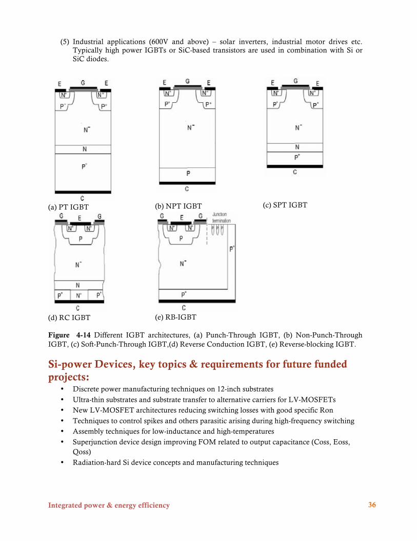
Integrated power & energy efficiency
36
(5) Industrial applications (600V and above) – solar inverters, industrial motor drives etc. Typically high power IGBTs or SiC-based transistors are used in combination with Si or SiC diodes.
(a) PT IGBT
(b) NPT IGBT
(c) SPT IGBT
(d) RC IGBT
(e) RB-IGBT
Figure 4-14 Different IGBT architectures, (a) Punch-Through IGBT, (b) Non-Punch-Through IGBT, (c) Soft-Punch-Through IGBT,(d) Reverse Conduction IGBT, (e) Reverse-blocking IGBT.
Si-power Devices, key topics & requirements for future funded projects:
• Discrete power manufacturing techniques on 12-inch substrates
• Ultra-thin substrates and substrate transfer to alternative carriers for LV-MOSFETs
• New LV-MOSFET architectures reducing switching losses with good specific Ron
• Techniques to control spikes and others parasitic arising during high-frequency switching
• Assembly techniques for low-inductance and high-temperatures
• Superjunction device design improving FOM related to output capacitance (Coss, Eoss, Qoss)
• Radiation-hard Si device concepts and manufacturing techniques

Integrated power & energy efficiency
37
Figure 4-15 Landscape of selected power applications vs. total current and voltage rating.
Figure 4-16 Typical power components usage vs. current and voltage rating.

Integrated power & energy efficiency
38
SiC Power semiconductor devices
Mikael Östling (KTH) With the contribution of:
Anton Bauer (Fraunhofer IISB) Wolfgang Dettmann (Infineon) Klaus Heyers (Bosch) Angelo Magrì (STMicroelectronics) Joachim Pelka, (Fraunhofer VµE) Lothar Schindele (Bosch)
Abstract
This subsection will focus on the state of the art in silicon carbide power device technology. A general overview will be presented on the status of silicon carbide wafer quality and availability. The section is divided into 8 parts starting with rectifying devices such as PN, PiN and Schottky devices for low loss and low on resistance. A brief discussion on possible switching speed advantage by using SiC devices vs traditional Si devices will be included. Size and weight advantages will be demonstrated.
The second part will focus on current and future MOSFET devices. Fabrication strategies as well as a discussion on fundamental and practical performance limitations are included. A special focus will be on oxide properties and hence channel mobility.
The third part is devoted to JFET devices and fabrication strategies. Current device ratings and availability as well as device types are discussed. Both normally-on and normally-off devices will be discussed as well as high temperature properties.
The fourth part concerns bipolar junction transistors. Also here current fabrication strategies and device designs will be explored. A paragraph will also be devoted to operation under harsh environments. High voltage design above 3 kV will be included as well as high voltage junction termination extension structures.
Introduction Silicon carbide (SiC) semiconductor devices for high power applications are now
commercially available as discrete devices. Schottky diodes are offered since several years by both USA and Europe based companies. Active switching devices such as bipolar junction transistors (BJTs), field effect transistors (JFETs and MOSFETs) have also reached the market recently. The interest is rapidly growing for these devices in high power and high temperature applications. The main advantages of wide bandgap semiconductors are their very high critical electric field capability. From a power device perspective the high critical field strength can be used to design switching devices with much lower losses than conventional silicon based devices both for on-state losses and reduced switching losses.
Several scientific papers have been published and comprehensive textbooks, book chapters and invited papers have been written on SiC power devices and process technology and the readers are referred to [Zetterling2002, Östling2010MRS, Östling2010IEDM, Zetterling2012] and references therein. The device technology is greatly dependent on substrate and epitaxial material quality and the number of detrimental defects. Over the years this has been one of the limiting

Integrated power & energy efficiency
39
factors for a commercial success of the high voltage and high current device market. Today the materials quality of 4H-SiC wafers and epitaxy is at such a high quality that many companies are offering commercial SiC wafers and epitaxy on 4H-SiC with wafer diameter with reasonable lifetime and low basal plane dislocation density 100 mm.
The key figure of merit for power switches is the so called on-resistance Ron. This parameter tells directly how much resistive loss a device generates in the forward conduction mode. The Ron is usually given in mΩcm2 and can be calculated from equation 1 below by:
𝑅!" =!
!!!!!= !!!
!
!!!!!! (1)
where VB denotes the breakdown voltage and Ec the critical electrical field. Since the Ec of
4H-SiC is about 7-8 times higher than that of Si one can easily understand the enormous advantage of using SiC devices.
In Figure 4-17 the theoretical unipolar limits comparing Si and SiC are depicted. Many reports have been published with commendable device results approaching close to the theoretical limit. In a recent paper by Zetterling, C.M. [Zetterling2012] a table of device performances is presented on current commercially available SiC devices, see
Table 4-1. It is encouraging to see that several of the published data by commercial companies [CreeWeb, RohmWeb, SemisouthWeb, InfineonWeb, GenesicsemiWeb, TransicWeb,], i.e. Cree, SemiSouth and TranSiC, refer to data for large devices. Many university data are made on small devices.
Figure 4-17 Theoretical breakdown voltage vs Ron

Integrated power & energy efficiency
40
Table 4-1 Recently published commercial devices presented by respective company.
High voltage blocking A high blocking voltage is a key feature for SiC power devices. The electric field crowding at
the edge of the junction is usually the main cause for the device breakdown. Hence, an efficient and easy to fabricate junction edge protection or termination must be implemented. A mesa design integrated with junction termination extensions (JTEs) is shown to be a very effective approach. The JTE can be formed in several ways. A common way is by ion implantation which can be easily implemented but creates lifetime-killing defects in SiC that act as recombination centers and results in smaller common emitter current gain (β). Furthermore ion implantation needs high temperature annealing to activate the implanted dopants which cause crystal damage and surface roughness [Ghandi2009]. This extra step also affects the performance of the fabricated device. An alternative to avoid ion implantation steps in the device fabrication is the etched epitaxial junction termination extension which also results in lower fabrication cost. In general, high breakdown voltage calls for a large area junction termination which becomes costly.
SiC diodes/rectifiers The main application areas for SiC diodes are in power factor correction circuits (PFC),
power supplies and recently in photovoltaic (PV) inverters as free-wheeling diodes in parallel with an inductive load, to limit the overvoltage on the switch, or in the rectifiers. The main advantage of the SBD is the almost zero reverse recovery current during switching. Hence it is possible to increase the switching frequency considerably. This in turn makes it possible to significantly decrease the volume, weight and cost for the system because all passive components such as inductors and capacitors can be made smaller. Generally a minimum low forward voltage drop is desired. Specifically for SiC is that the series resistance in the drift layer can be made very low because of high doping and thin layer thickness. The high bandgap makes the pn-junction built in voltage very high and less advantageous than using a Schottky metal. Also for the Schottky contact the built-in voltage is much higher than for silicon but still low enough to favour a low forward voltage drop. Moreover the leakage current is very low because of the comparably higher Schottky barrier height. For voltages beyond 1-2 kV a combination of a pn-diode structure and a Schottky diode design referred to as the Junction Barrier Schottky (JBS) [Hallén2010] or Merged PiN Schottky (MPS) are preferred because of the superior reverse blocking and surge current capability. A popular application for the SiC JBS diode is as a free-wheeling diode for a Si IGBT where the switching frequency can be increased.
Switch devices The maturity of SiC is evident from the commercial availability of SiC switches for high
voltage applications. At this point 1200 V and some 1700 V devices are available, see Table I.

Integrated power & energy efficiency
41
Interestingly several device types are competing in this range: bipolar transistors, JFETs and MOSFETs. The Si CoolMOS dominates the voltage range up to 900 V, but above 1 kV the SiC devices have to compete with the Si IGBT. The forward voltage drop of the switches is dominated by the on-resistance of the blocking region as analyzed before, but other parasitic resistances have to be included as well.
JFETs The vertical junction field effect transistor (JFET) can be made as a normally-on or normally
off device, depending on the doping and spacing between the gates. Apart from the on-resistance of the blocking region, a pinch region resistance is added. The tradeoff between a small pinch resistance (normally-on design) and a larger pinch resistance (normally-off design) depends on the application demands. The high input impedance and voltage control makes it an attractive switch. Two main variants exist: the trench type structure and recently Infineon released a version called CoolSiC wich features a lateral pinch region that includes a built-in body diode.
The fabrication process of JFETs is quite straight forward. The main drawback with VJFETs is that they are usually normally-on (depletion mode), which is considered unsafe in power applications. Recently SemiSouth has demonstrated normally-off VJFETs. The operational threshold voltage margin is however limited for such a device and they may have a limited temperature of operation. JFETs exhibit a small capacitance and can thus be operated at high switching speed. From a reliability issue JFETs are considered as very promising since they rely primarily on pn-junction operation and not dependent on the quality of gate control dielectrics. SiC JFETs provide excellent high temperature operability. The potential for very high voltage operation is limited since the device operation relies on unipolar device operation and hence the Ron is proportional to the breakdown voltage.
MOSFETs The most desired power device to date is the vertical power MOSFET. It operates normally-
off (enhancement mode) and with small current demand on the drive circuits. The SiC vertical MOSFET is similar to the Si DMOSFET, except all doping is done using ion implantation. The on-resistance consists of the same three parts as for the JFET: the on-resistance of the blocking region, the pinch region resistance and the channel resistance. The most challenging part in the SiC MOSFET is the channel mobility which is very low because a large part of the channel charge is trapped in the oxide interface. The main drawbacks are the questionable reliability because of the sensitive gate dielectrics and the relatively poor channel mobility under the gate dielectrics. The low mobility gives the MOSFETs a relatively high Ron for medium breakdown voltage (<2kV). Recently Cree’s 1200V MOSFET family was introduced on the market. Although the MOSFET can be driven by a gate over-voltage so that channel charge can be increased (and hence lower resistance), recommendations are to keep the maximum electric field below about 3 MV/cm across the gate dielectrics to avoid reliability issues. The same concern is also in the reverse bias direction.
Bipolar Junction Transistors The bipolar junction transistor (BJT) main advantages as power switch are its low
conduction loss combined with fast switching. The BJT potentially has the lowest voltage drop among the switch devices. The BJT operation in the forward direction is beneficial for reaching a low on-state loss since the two built-in pn-junctions cancel each other, hence the on-state loss is mostly dependent on the drift layer resistance and the contact resistance. As substrate- and epi-materials become better the minority carrier lifetime will be high enough so that by conductivity modulation of the low doped collector region under high injection conditions the on-resistance could be further reduced. However, at present this is not yet fully demonstrated. Traditionally, Si BJT was not the preferred device at high voltages, because of the relatively low base doping level

Integrated power & energy efficiency
42
causing base push out at high injection, also known as the Kirk effect. The SiC BJTs higher doping concentration delays the onset of the Kirk-effect. One main advantage with the SiC BJT is that the SiC BJT is a normally-off device that does not have a sensitive gate oxide. However, it is a current controlled device, and depending on current gain, the gate drive circuit can consume some power. SiC BJTs are easy to connect in parallel. Increased complexity in drive circuitry and the moderate current gain are drawbacks of BJTs compared to FETs, whereas a normally-off characteristic in the BJT is an advantage over the JFET. The BJT is extremely robust with high surge current capability, high temperature performance and high cosmic-ray radiation hardness [Hallén20]. The table below lists some commendable BJT results.
Very High Voltage - High Injection Devices Devices for very high voltage beyond 5 kV require ultimate materials quality for two main reasons. Firstly, at these high voltages defects in the material will cause immature breakdown and secondly, in order to yield a reasonable low on-resistance the devices must operate during high injection which also calls for ultimate high quality SiC wafers with a minimum basal plane dislocation density.
Concluding remarks and Issues of concerns for SiC power devices The market of SiC commercial devices is rapidly increasing. Commendable performances on
both SiC Rectifiers , JFETs, MOSFETs and BJTs are already available. Some concerns for the future R&D activities should include;
1. Substrate size and defect control with respect to carrier lifetime, killing defects and basal plane dislocation density.
2. Reduced cost of the wafer fabrication process and the epitaxial growth process is a must 3. Establishment of a competitive European supply chain for SiC wafers. 4. Serious research activities must be devoted to Junction termination Extensions for high
voltage junction and surface termination geometries and efficient and low cost structure manufacturing technology.
5. Larger device areas must be explored. 6. MOSFETs channel resistance must be substantially improved. Subsequent research on gate
dielectric technology must be emphasized. 7. New and improved contact technologies must be engineered to yield lower contact
resistance at lower process temperatures.
Ref Title Author Year BV (V)
Ron
(mΩ.cm2) Current gain β
Ryu2000 1800 V, 3.8 A bipolar junction transistors in 4H-SiC
S. H. Ryu
2000 1800 10.8 20
Domeij2010 2.2 kV SiC BJTs with low VCESAT fast switching and short-circuit capability
M. Domeij
2010 2200 4.5 35
Zhang2004 10 kV, 10 A Bipolar Junction Transistors and Darlington Transistors on 4H-SiC
J. Zhang 2010 10000
130 28
Ghandi2011
High-Voltage (2.8 kV) Implantation-Free 4H-SiC BJTs With Long-Term Stability of the Current Gain
R. Ghandi
2011 2800 4.5 55
Miyake2012 21-kV SiC BJTs With Space-Modulated Junction Termination Extension
H. Miyake
2012 21000
321 63

Integrated power & energy efficiency
43
8. Very high voltages above 10 kV are fairly little explored in SiC and need to be addressed properly.
References [CreeWeb] http://www.cree.com/power/products [Domeij2010] M. Domeij et al., “2.2 kV SiC BJTs with low VCESAT fast switching and short-‐circuit
capability,” Materials Science Forum, vol. 645-‐648, pp. 1033-‐1036, 2010. [Ghandi2009] R. Ghandi, B. Buono, M. Domeij, G. Malm , C.-‐M. Zetterling, and M. Östling, “High
voltage 4H-‐SiC PiN diodes with etched junction termination extension,” IEEE Electron Device Lett., vol. 30, pp. 1170-‐1172, 2009
[Ghandi2011] R. Ghandi, B. Buono, M. Domeij, C.-‐M. Zetterling, and M. Östling, “High Voltage (2.8 kV) Implantation-‐free 4H-‐SiC BJTs with Long-‐Term Stability of the Current Gain,” IEEE Transactions on Electron Devices, vol. 58, no. 8, pp. 2665 -‐ 2669, 2011.
[GenesicsemiWeb] http://www.genesicsemi.com/index.php/sic-‐products [Hallén2010] A. Hallén, M. Nawaz, C. Zaring, M. Usman, M. Domeij, and M. Östling, ”Low-‐
temperature annealing of radiation-‐induced degradation in 4H-‐SiC bipolar junction transistors,” IEEE Electron Device Lett., vol. 31, pp. 707-‐709, 2010.
[InfineonWeb] http://www.infineon.com/cms/en/product/index.html [Miyake2012] H. Miyake, T. Okuda, H. Niwa, T. Kimoto, and J. Suda, “21-‐kV SiC BJTs With Space-‐
Modulated Junction Termination Extension,” IEEE Electron Device Letters, vol. 33, no. 11, pp. 1598–1600, Nov. 2012
[Östling2010MRS] M. Östling et al “SiC Bipolar Power Transistors -‐ Design and Technology Issues for Ultimate Performance” in Silicon Carbide 2010 — Materials, Processing, and Devices, edited by S.E. Saddow, E. Sanchez, F. Zhao, M. Dudley (Mater. Res. Soc. Symp. Proc. Volume 1246, Warrendale, PA, 2010, B08-‐01,
[Östling2010IEDM] M. Östling, Silicon Carbide Based Power Devices, International Electron Devices Meeting, 2010 INTERNATIONAL ELECTRON DEVICES MEETING -‐ TECHNICAL DIGEST, pp. 13.3.1-‐13.3.4, International Electron Devices Meeting (IEDM), San Francisco, CA, DEC 06-‐08, 2010.
[RohmWeb] http://www.rohm.com/products/sic/ [Ryu2000] S.-‐Hyung Ryu, A, A. K. Agarwal, R. Singh, and J. W. Palmour, “1800V , 3 . 8A Bipolar
Junction Transistors in 4H-‐Sic,” in DRC, 2000, vol. 19, no. 12, pp. 133-‐134. [SemisouthWeb] http://semisouth.com/power-‐semiconductors [TransicWeb] http://www.transic.com/ [Zhang2004] J. Zhang, J. H. Zhao, P. Alexandrov, and T. Burke, “Demonstration of first 9.2 kV 4H-‐
SiC bipolar junction transistor,” Electronics Letters, vol. 40, no. 21, pp. 49-‐50, 2004. [Zetterling2002] C.-‐M. Zetterling (Ed.), “Process technology for silicon carbide devices,” Institution
of Electrical Engineers, 2002. [Zetterling2012] C.-‐M. Zetterling,.Present and future applications of Silicon Carbide devices and
circuits, Custom Integrated Circuits Conference (CICC), 2012 IEEE, San Jose, CA, Proceedings, p.1-‐8

Integrated power & energy efficiency
44
Power GaN Device Technology
Steve Stoffels (IMEC) With the contribution of:
Oliver Ambacher (Fraunhofer IAF) Jean Jacques Aubert (CEA – Leti) Angelo Magrì (STMicroelectronics) Gaudenzio Meneghesso (University of Padova and IUNET) Peter Moens (ONsemiconductor) Joachim Pelka, (Fraunhofer VµE) Jan Sonsky (NXP)
Abstract
In this subsection the GaN power device technology will be explained starting from a general overview of the device architecture and device physics. Several inherent device challenges will be discussed in more detail, such as ohmic contacting, e-mode operation and the engineering of the device to achieve high breakdown. The subsection is split in six parts.
The first part will give a general overview of the GaN material and basic device physics such as polarization effects and 2DEG formation at the heterojunction to serve as a basis for the remainder of the section.
In the second part the different device architectures will be looked at into more detailed and an overview given of how they are fabricated. First, the high electron mobility structure with a Schottky gate (HEMT) will be discussed. The following structure, which will be discussed a HEMT with an insulated gate (i.e. dielectric under the gate). Thirdly the different options for achieving vertical GaN devices will be investigated. And finally the technology for making bi-directional switches in GaN will be detailed.
The third part of the section will explain the process of the formation of ohmic contacts with a low contact resistance. Processes existing in literature will be investigated and attention will be spent to identify the different metal alloy systems used for achieving these contacts.
The fourth part handles about depletion mode (d-mode) versus enhancement (e-mode) device concepts. In its natural state, the GaN/AlGaN material system tends towards the formation of a highly conductive electron gas at its interface (2DEG) and devices are thus normally d-mode. In this part several concepts will be investigated which can lead to e-mode operation. Namely recessing of the gate region, fluoride treatment of the gate region or growing p-type layers to deplete the channel.
The fifth part will detail ways to increase the breakdown voltage of GaN devices and inherent limitations. GaN is normally grown in a heteroepitaxy step on a foreign substrate due to the inherent costs of intrinsic GaN substrates. This growth can lead to problems at the interface between the substrate and GaN epitaxial stack, which can limit the breakdown of the GaN components. This section will describe the issue and solutions to this problem. These solutions are

Integrated power & energy efficiency
45
the engineering of the GaN buffer to withstand higher breakdown voltages or cut the conductive paths at the GaN substrate interface by either substrate implantation or removal.
The sixth and last part will describe limitations on real performances in the application environment due to traps presence either at semiconductor interfaces or the epitaxial material. The trapping and de-trapping mechanism will affect the application, increasing Rds,on in switching condition or limiting maximum power at high frequency. This section will describe issues and solutions to mitigate this problem. Solutions could come from surface passivation, cleaning of interfaces or from engineering of the epitaxial stack.
GaN material and device physics The physics underpinning the transistor action in GaN HEMTs in completely different from
traditional silicon components. In Si it is necessary to dope the material to create n- or p-type regions whose interaction leads to the physical behavior of the component. In the AlGaN/GaN material systems no dopants are used to create the highly conductive channel layer, rather it is an interplay between the electronic and piezoelectric behavior of the material which leads to the formation of the highly conductive channel, also named two dimensional electron gas (2-DEG) [Mishra2002]. Because of these fundamental differences, it is necessary to understand at least at a fundamental level the physics behind the component, which will be explained in this section.
The III-V nitrides (AlGaN/GaN/InGaN/InAlGaN) all have a hexagonal wurtzite crystal structure. This crystal structure is non axisymmetric and mechanical deformation will lead to a polarization of the material, this polarization leads to a net excess (bound) charge layer on one interface of the material and the opposite charge at the other end of the material [Mishra2002]. The sign of this charge depends on whether the material is terminated with a Ga (Ga-face) or a N (N-face). The GaN-based material will then be naturally polarized (as grown) and this is called spontaneous polarization. For the most common growth technique (MOCVD), however the material will always be terminated with a Ga face and have negative bound charges at this interface.
Figure 4-18 Polarization charges in Ga- and N-face AlGaN/GaN Heterostructures
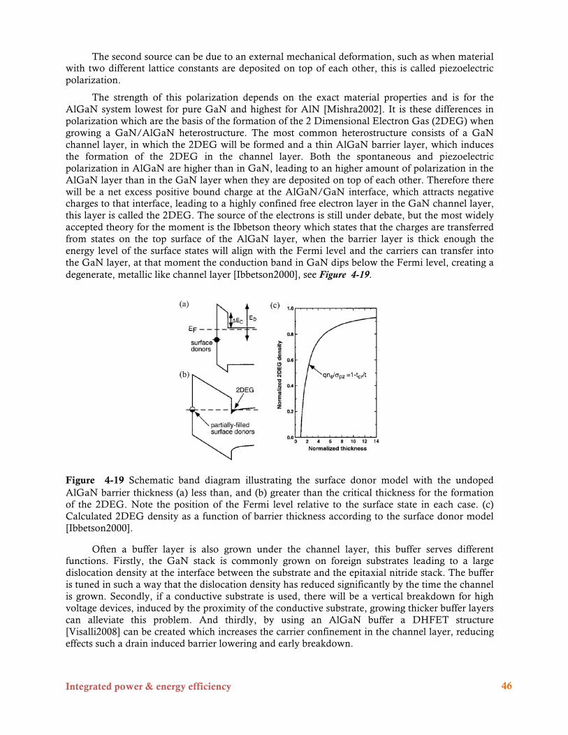
Integrated power & energy efficiency
46
The second source can be due to an external mechanical deformation, such as when material with two different lattice constants are deposited on top of each other, this is called piezoelectric polarization.
The strength of this polarization depends on the exact material properties and is for the AlGaN system lowest for pure GaN and highest for AlN [Mishra2002]. It is these differences in polarization which are the basis of the formation of the 2 Dimensional Electron Gas (2DEG) when growing a GaN/AlGaN heterostructure. The most common heterostructure consists of a GaN channel layer, in which the 2DEG will be formed and a thin AlGaN barrier layer, which induces the formation of the 2DEG in the channel layer. Both the spontaneous and piezoelectric polarization in AlGaN are higher than in GaN, leading to an higher amount of polarization in the AlGaN layer than in the GaN layer when they are deposited on top of each other. Therefore there will be a net excess positive bound charge at the AlGaN/GaN interface, which attracts negative charges to that interface, leading to a highly confined free electron layer in the GaN channel layer, this layer is called the 2DEG. The source of the electrons is still under debate, but the most widely accepted theory for the moment is the Ibbetson theory which states that the charges are transferred from states on the top surface of the AlGaN layer, when the barrier layer is thick enough the energy level of the surface states will align with the Fermi level and the carriers can transfer into the GaN layer, at that moment the conduction band in GaN dips below the Fermi level, creating a degenerate, metallic like channel layer [Ibbetson2000], see Figure 4-19.
Figure 4-19 Schematic band diagram illustrating the surface donor model with the undoped AlGaN barrier thickness (a) less than, and (b) greater than the critical thickness for the formation of the 2DEG. Note the position of the Fermi level relative to the surface state in each case. (c) Calculated 2DEG density as a function of barrier thickness according to the surface donor model [Ibbetson2000].
Often a buffer layer is also grown under the channel layer, this buffer serves different functions. Firstly, the GaN stack is commonly grown on foreign substrates leading to a large dislocation density at the interface between the substrate and the epitaxial nitride stack. The buffer is tuned in such a way that the dislocation density has reduced significantly by the time the channel is grown. Secondly, if a conductive substrate is used, there will be a vertical breakdown for high voltage devices, induced by the proximity of the conductive substrate, growing thicker buffer layers can alleviate this problem. And thirdly, by using an AlGaN buffer a DHFET structure [Visalli2008] can be created which increases the carrier confinement in the channel layer, reducing effects such a drain induced barrier lowering and early breakdown.

Integrated power & energy efficiency
47
Device architectures
HEMT (Schottky) The high electron mobility transistor (HEMT) is the most investigated transistor structure in
the AlGaN/GaN system. The channel layer of the transistor is the 2DEG, described above. To form a transistors, three thermals are needed, a source and drain contact to conduct the current and a gate contact to modulate the current in the channel. The source and drain contact need to be ohmic contacts, to have a low resistive path for the current to flow. The gate contact was traditionally a Schottky contact, with a high work function (e.g. Ni, Pt, Mo, Ir) to create a barrier which blocks the current flow, but allows a modulation of the channel [Khan1993, Khan1994, Ueda2005]. The Schottky gate performs well and is still used in production for RF-HEMT components nowadays. However the Schottky architecture has some limitations, firstly it has a high leakage current when a reverse blocking voltage is put over it. This limits the usefulness for high voltage applications, as these components need to be able to withstand very high blocking voltage (~600V), with low leakage. The requirement for power transistors is normally a five decade difference between on-state and off-state current, which for GaN translates in a leakage current (<1µA/mm). Secondly, the maximum gate overdrive is limited because the Schottky gate opens around 2V. In a switching circuit this limits the maximum speed at which the component can be switched.
The 2DEG is naturally formed in the AlGaN/GaN system and is present without any applied external potential. The HEMTs are therefore normally on (Depletion mode, D-mode), i.e. a negative voltage needs be applied to switch off the device. The voltage required to switch of the components is also called the threshold voltage (Vth) that is negative ion D-mode devices. For power transistors normally OFF devices are preferred (Enhancement mode, E-mode) because it allows the component to naturally switch off in case of failure of the gate driver. Therefore much research effort is being spend on developing E-mode operation for GaN components. Several of these technologies are discussed later.
MIS-HEMT A MISHEMT is a type of HEMT with an insulated gate instead of a Schottky gate. This gate
architecture was developed The main motivation to introduce such a gate is to allow a reduction in gate leakage and to increase the maximum gate overdrive. It has been shown in several publications that the leakage current can be decreased from the typical mA/mm for Schottky gate structures to nA/mm for insulated gate structures [Sugimoto2005, Chen2011, VanHove2012, Fontsere2012]. Maximum gate voltages of 10V or higher can easily be achieved with these insulated gate structures.
Vertical devices Vertical devices are possible to fabricate from intrinsic GaN wafers and have shown good
performance, but are currently too expensive. GaN wafers suitable for vertical devices are about three orders of magnitude more expensive than silicon wafers, and this for a maximum wafer size of 2 inch which is currently available [Yole2010].
Another route to fabricate vertical components is to grow a highly conductive n+ GaN layer below the buffer layer during the epitaxial growth of the GaN stack. Etching the buffer and creating an ohmic contact to this n+ GaN allows the formation of a back contact. The maximum breakdown voltage of this component will be limited by the buffer thickness, which is limited due to cost and wafer bow restrictions.
Most AlGaN/GaN power HEMTs are horizontal devices, however, in high voltage applications, vertical transistors are highly preferred due to their lower parasitic inductance, higher blocking voltage, and smaller size. There have been several reports on GaN vertical transistors such as the Current Aperture Vertical Electron Transistor (CAVET) [Chowdhury2008] and the vertical

Integrated power & energy efficiency
48
trench gate GaN MOSFET [Otake2008], but they all suffer from either high leakage current or poor channel mobility. Furthermore, they were fabricated on expensive bulk GaN substrate, which makes their commercialization very challenging. Moreover for this concept the excellent properties of the 2DEG can not be exploited and vertical devices will therefore have higher on-resistances, making them less attractive for power applications.
Ohmic contacts Much work has been performed on achieving good and reliable ohmic contact the 2DEG in
an AlGaN/GaN heterostructures. This is a non-trivial task due to the large bandgap of the nitride materials. There are two main routes which have been followed to create ohmic contacts. The first is to deposit a low work function metal on top of the AlGaN, followed by an ohmic alloy to create the ohmic contact. The second route is to regrow the contact with a highly doped n+ GaN layer to create a reliable and low resistive contact.
The most commonly used metallization scheme that gives good and reliable ohmic contacts is the Ti/Al/x/Au contact, where x is a diffusion barrier such as Mo/Ni [Bright2001, Gong2010, VanDaele2005]. Ti and Al react with the AlGaN to form TiN and AlN, extracting N from the AlGaN and leaving N vacancies behind. The N vacancies act as donors, allowing the formation of a low resistive tunnel contact through the barrier. Au should act as a low resistive top metallization for easy interconnection, however in practice it is seen that Au diffuses out and plays a role in creating low ohmic contacts. Contact resistances achieved with this metallization scheme are often quotes around 0.5 ohm·mm or lower. This is good enough to form a reliable contact to the AlGaN, there are however some doubts about the stability and cost of this process.
The current industry drive is to implement GaN technology on an industry standard CMOS fab with wafer sizes starting at 150mm, but scaling up to 200mm to drive costs further down. The GaN process could be established next to existing CMOS lines to cut costs and make use of those high productivity fabs. However, to make use of these fabs all processes should be CMOS compatible, which means that Au containing contacts can not be used, as Au acts as a source of contamination and yield killer for Si. There is thus a need to also develop Au-free contacts. There have been several reports in literature of Au free contacts [DeJaeger2012, Lee2011], use a Ti/Al/W metal stack achieving a contact resistance of 0.49 Ω·mm. It was shown that ohmic recess has a positive impact on the contact resistance, and was essential to achieve a contact resistance below 0.5 Ω·mm [Lee2011]. Substitution of Au with Ag and using V instead of Ti in a V/Al/V/Ag stack by Miller et al. [Miller2008, Miller2008b], has lead to low contacts of 0.27 Ω·mm, however Ag is, just as Au, not a desirable material in CMOS processing, so further work is needed to make the V contacts CMOS compatible.
To reduce contact resistances even further, it is possible to etch of the AlGaN barrier and GaN channel and regrow a highly doped n+ GaN layer. The top metalization on this n+ layer does not require any further annealing. Contact resistance values as low as 0.153Ω·mm have been shown in literature for MOCVD [Huang2012], and 0.035Ω·mm for MBE regrowth [Faria2012]. These results indicate a route to achieve ultra low contact resistances for GaN transistors, albeit at slightly higher cost than pure metal contacts.
E-mode devices In previous sections it was explained that the 2DEG is naturally present in the AlGaN/GaN
heterostructure and therefore the HEMT transistors fabricated from this heterostructure are naturally on (D-mode), for the most common device geometry the Vth usually lies around -3V. For safety and reliably concerns for high voltage/power devices it is actually preferred to have a device which is normally off (E-mode). Therefore extra effort is needed to achieve AlGaN/GaN HEMTs which can achieve E-mode operation. Most techniques modify the region by introducing extra processing steps, which modify the charge density near the gate with respect to the rest of the

Integrated power & energy efficiency
49
component. There is however also the option to put the GaN transistor in series with a low voltage silicon E-mode component (cascade) to achieve E-mode operation for the overall layout. In this section several techniques recently reported to achieve E-mode will be discussed.
Thin AlGaN gate barrier One of the most straightforward ways to achieve e-mode operation is to recess the AlGaN
barrier in the gate region. According to the Ibbetson theory for the 2DEG formation [Ibbetson2000], there is a critical thickness tcr for the AlGaN barrier, below which the 2DEG does not form. It has been shown in literature [Ota2009, Maeda2012], that by performing a recess etch of the gate region, before deposition of the gate metal, the Vth can be shifted to more positive values. An alternative implementation was shown by [Derluyn2009], the authors exploit the fact the in-situ grown Si3N4 increased the electron density in the channel. Combining a thin barrier with an in-situ grown Si3N4, allows for a relatively low access resistance in the source, drain regions, while the removal of the in-situ Si3N4 in the gate region leaves only the thin barrier layer, which depletes the region under the gate. Currently a maximum positive Vth of around 0.5V is achieved using the various type of “thin gate barrier” techniques. Challenges remain to scale further to values around 2V-4V, which are required by industry.
Charge incorporation The second way in which to increase the threshold voltage is to incorporate negative charges
in the gate electrode, which can compensate the charges in the 2DEG and thus deplete the gate region, achieving E-mode operation. Several ways have been presented in literature to achieve the charge incorporation.
The first ways is by treating the surface of the gate with a fluorine based plasma [Cai2005, Chen2011b]. This treatment will implant negatively charged F- ions in the barrier/cap/dielectric layer. Positive shifts up to a Vth of 1V have been observed [Cai2005]. There are some lingering concerns about stability of the implantation which are still unresolved.
P-GaN or p-AlGaN gate structure Growing a p-type GaN or AlGaN layer in the gate region is another way to introduce
compensating charges in the gate region [Suh2006, Uemoto2007, Hwang2012]. Tuning the thickness and doping concentration in the p-type layer allows to achieve high threshold voltages, which can be as high as 3V [Hwang2012]. P-type layers are currently the most promising route to achieve high threshold voltages, however these devices suffer from slightly increased on-resistances, with respect to D-mode devices, due to a decreased carrier concentration in the channel. Authors have also used a doped gate oxide (NiO) to introduce compensating charges [Kaneko2009] at the gate region. A Vth of 0.8V was demonstrated by the authors.
HEMT/FET Hybrid Another approach to e-mode is to fabricate a hybrid HEMT/FET transistor, where the
access regions (source/drain) are formed by a 2DEG, while the gate control is achieved by the attraction of electrons which form a channel layer under the gate, similar as to what happens for silicon MOSFET’s [Oka2008, Kambayashi2009, Medjoub2010, Li2012]. For this approach authors etch of the GaN channel and form a MISFET/MOSFET type gate. Threshold voltages of 2.8V have been demonstrated for this approach [Kambayashi2009]. The disadvantage of this approach is the increased on-resistance due to the presence of a MOSFET region under the gate, which has a higher access resistance than the equivalent 2DEG structure.

Integrated power & energy efficiency
50
Cascode The final approach to E-mode, which has been investigated in the literature, is to combine
connect a D-mode GaN in series with a low voltage E-mode Si transistor [micro2012], forming in this way a cascode structure. The GaN transistor will deliver the blocking voltage needed for high voltage application, while the Si transistor delivers the necessary gate control such that the cascode structure switches on for positive gate voltages. Advantages of this are that a well developed GaN D-mode transistor can be used for creating the cascode, the D-mode transistors are much better developed than the E-mode GaN transistors and can deliver lower on-state resistance, lower leakage current and better understood reliability. The disadvantage is that due to the presence of a second Si component, it will slightly increase the price, complexity and on-resistance with respect to an isolated D-mode GaN transistor (due to the low voltage nature of the Si transistor, the on-resistance increase is still acceptable).
Breakdown voltage engineering and limitations One of the critical parameters for any high power semiconductor technology is the
maximum blocking voltage that the components can withstand. GaN is an excellent material from this perspective, because the critical electrical field in the material is around 3.3MV/cm, which is around 10 times higher than silicon and 10 percent higher than SiC. Nonetheless there are critical challenges left to achieve high breakdown voltages during device operation.
The main parameter to scale when increasing the breakdown voltage is the distance between the gate to drain (LGD) terminals of the transistor. The larger distance will make sure that the critical breakdown field in GaN is reached for higher drain voltages. The tradeoff is that by increasing the LGD, the on-resistance (RON) is also increased due to the increased path length through the semiconductor.
The main route that is being followed to fabricate cost effective GaN powertransistors to grow the heteroepitaxy on top of a cheap silicon substrate [Marcon2012, Cheng2012, DeJaeger2012]. This adds some extra complexities while striving to achieve high breakdown voltages. Due to the presence of a semi-conducting silicon substrate, charges can accumulate at the interface between the GaN buffer and the silicon substrate [Visali2011]. Due to this phenomenon, a vertical “buffer” breakdown can occur in the component, limiting the maximum achievable breakdown for a certain GaN epi stack. The challenge for GaN-on-Si powercomponents is to optimize the buffer, interface or substrate in such a way that high breakdown voltages can be achieved. There are several routes, which can be followed; one is to optimize the AlGaN/GaN buffer structure to reach high breakdown voltages. Another path is to work on the charge accumulation at the silicon interface; in fact by cutting the path for the electrons to flow, it is possible to increase the breakdown voltage. Examples are the implantation of the silicon near the buffer/Si interface [Umeda2010] to inhibit the charge accumulation under the contacts or the removal of silicon after the device processing has been completed [Srivastava2011] which eliminates the charge accumulation.
An important note is that due to the lateral nature of the GaN-on-Si technology, there is a limit to how far the breakdown can be scaled before the costs of the component becomes inhibitive. Even if the vertical buffer breakdown can be eliminated, the lateral breakdown will be limited by the spacing between the gate and drain contact. Therefore the only way to increase the breakdown is to increase the size of the component and thus the cost.
Buffer engineering Often, the limiting factor in scaling to higher voltages is the buffer layer, under the GaN
channel. Increasing the complexity of the buffer is therefore an obvious route to explore to achieve higher breakdown values. One of the routes that has been followed is scaling the buffers to higher thicknesses [Alrulkaman2005, Ikeda2008, Ikeda2010], as was demonstrated by researchers of the

Integrated power & energy efficiency
51
Yokohoma R&D labs at Furukawa Electric Company. They have demonstrated 7µm thick buffers and a breakdown voltage exceeding 2kV [Ikeda2010. However, these demonstrations were limited to small wafer sizes; scaling up to large wafer sizes, which is necessary to reduce costs in production, will be challenging. This is because the growth of thick AlGaN/GaN stacks on silicon causes significant amounts of stress, leading to wafer bow and cracking. Secondly, the growth of these layers is fairly slow and growing thicker buffers will increase costs significantly.
Another technique that has been used to improve the breakdown is the doping of the buffer with Fe [Choi2006, Oshimura2011] or C [Hilt2011]. This suppresses early breakdown occurring at the buffer/AlN/Si junction. Devices with this type of buffer exhibit more consistent and enhanced breakdown voltages compared to devices without Fe or C doping. However, while for this case it is possible to get closes to the intrinsic material limit, the breakdown will still be limited by the buffer thickness.
Substrate implantation Panasonic proposed to modify the substrate properties in order to increase the blocking
voltage [Umeda2010]. Their concept was called Blocking Voltage Boosting and consisted of a selective ion implantation to create p+ regions at the periphery of the transistor. Implanting these regions inhibits the electrons flowing between the bottom substrate contact and the source/drain, effectively doubling the maximum achievable breakdown voltage. They showed an improvement from 780V to 1500V for the non-implanted versus implanted structure. This structure is very effective in cutting the path between the contacts and the substrate, however there is still a path through the silicon between source and drain. The breakdown will thus still be limited by the buffer thickness, the technology will need to be developed further to also address these issues.
Substrate removal At IMEC an alternative technology has been developed to increase the breakdown voltage,
while at the same time maintaining a thin AlGaN buffer, such that costs and wafer bow can be kept under control, even for large wafer sizes. The approach followed was to perform a local silicon removal around the drain contact [Srivastava2011]. This removal effectively cuts the path for electrons to flow between source and drain and thus inhibits the charge accumulation, which leads to vertical breakdown. It has been shown that after the local silicon removal, the breakdown voltage of the transistors does not depend on the buffer thickness but rather is linear dependent on the gate-drain distance and has been shown to exceed 2kV, even for buffers as thin as 600nm. Therefore the local substrate removal technology proves to be a promising route for fabricating high voltage, cost effective GaN power transistors on large area silicon wafers. Future development should focus on making the technology compatible with grounded substrates, as currently it only works for a floating substrate.
Conclusion The research and development of GaN technology for power switching has made large
strides in the past decade, several key challenges have been addresses since the inception of GaN as a power technology. To succeed as a power technology, the transistors need to exhibit a high breakdown voltage, a low on-resistance, a low leakage current a positive threshold voltage, high stability, reliability and should be cost competitive (at least on system level) with established silicon technologies. It has been shown by several research labs, universities and companies that GaN components do exhibit figures of merit which are an order of magnitude better than what is achievable with silicon and even SiC. However several key issues remain.
Beyond the obvious challenge of scaling the technology to higher breakdown voltages and power levels, there were some other less obvious challenges. Historically GaN HEMT’s were grown on a SiC substrate. The high price of this solution would make it difficult for GaN to compete in the world of power electronics. To address this issue, researchers have introduced the
Integrated power & energy efficiency
52
GaN-on-Si technology which removed the expensive SiC substrate and leveraged the industrial strength of the large install base of silicon fabs. To ensure CMOS compatibility, necessary for processing in a silicon fab, all Au containing steps had to be removed from the process. This has meant a re-optimization of the ohmic contacts with silicon compatible metals. To secure the leadership of Europe in GaN technology, we need to make sure that we leverage the strength and cost competiveness of the GaN-on-Si technology and make targeted investments to bring this technology further along in its maturity level. An important step in reducing the overall costs of production is scaling up the wafer size to 200mm. First demonstrators have been shown on 200mm wafers, but further optimization is needed to increase yield, assess reliability and evaluate proper packaging techniques for these components. Furthermore, the ohmic metal stack and gate metal stack should be re-optimized to ensure silicon compatibility, while at the same time showing reproducibility, stability and a good performance. Contact resistance and gate leakage are key metrics for this optimization. Also, functional demonstrators for target applications would make a strong case for field testing the technology and identifying key issues in early stage of development.
Currently the only GaN devices on the market (EPC) have a maximum breakdown voltage of 200V. To capture larger portions of the market and assure market leading performance in 90% of the power market, it would be necessary to scale up the technology to at least 600V. Demonstrates in literature have shown breakdown voltages of 2000V, with record RonQg products, an order of magnitude below silicon. However, none of these technologies have been proven outside of research labs, and use tricks that might not be suited for large scale fabrication. Moreover, reliability and high voltage dispersion data has not been presented for these components and should all be addressed before high voltage GaN components can be introduced in the market. If Europe wants to play a leading role in this market, these issues should be addressed.
A final challenge for GaN devices, which would require dedicated research and investment is in achieving true e-mode operation. GaN devices are naturally depletion mode, which means that in the case of a gate driver failure, the device will conduct current, potentially destroying the entire system. This mode of operation is not preferred by system designers, who prefer e-mode. Currently manufacturers prefer to couple a well developed d-mode device with a low voltage silicon component in series. However, a high performance e-mode device would be the preferred solution from cost and performance perspective. If Europe wants to play a role in the future of GaN, resources should be spend on achieving reliable GaN transistors, with low on-state resistance and true e-mode operation. Several companies in US and Asia are heavily investigating these devices; therefore Europe cannot afford to miss the train.
References [Arulkumaran2005] S. Arulkumaran, T. Egawa, S. Matsui, and H. Ishikawa, “Enhancement of
breakdown voltage by AlN buffer layer thickness in AlGaN / GaN high-electron-mobility transistors on 4in . diameter silicon,” Applied Physics Letters, vol. 86, p. 123503, 2005.
[Binari2007] S. C. Binari, et al., Proc. IEEE, vol. 90, No.6, pp. 1048-1058, June 2007. [Bright 2001] A. N. Bright, P. J. Thomas, M. Weyland, D. M. Tricker, C. J. Humphreys, and R.
Davies, “Correlation of contact resistance with microstructure for Au / Ni / Al / Ti / AlGaN / GaN ohmic contacts using transmission electron microscopy,” Journal of Applied Physics, pp. 3143–3150, 2001.
[Cai2005] Y. Cai, Y. Zhou, K. J. Chen, and K. M. Lau, “High-Performance Enhancement-Mode AlGaN / GaN HEMTs Using Fluoride-Based Plasma Treatment,” IEEE ELECTRON DEVICE LETTERS, vol. 26, no. 7, pp. 435–437, 2005.
[Chen2011] K. J. Chen and C. Zhou, “Enhancement-mode AlGaN/GaN HEMT and MIS-HEMT technology,” Physica Status Solidi (a), vol. 208, no. 2, pp. 434–438, Feb. 2011.

Integrated power & energy efficiency
53
[Chen2011b] C. Chen, X. Liu, B. Tian, P. Shu, Y. Chen, W. Zhang, H. Jiang, and Y. Li, “Fabrication of Enhancement-Mode AlGaN / GaN MISHEMTs by Using Fluorinated Al2O3 as Gate Dielectrics,” vol. 32, no. 10, pp. 1373–1375, 2011.
[Cheng2012] K. Cheng et al., “AlGaN/GaN/AlGaN Double Heterostructures Grown on 200mm Silicon (111) Substrates with High Electron Mobility”, Appl. Phys. Express, Vol. 5, p. 011002 (2012).
[Choi2006] Y. C. Choi, M. Pophristic, H.-y. Cha, B. Peres, M. G. Spencer, and L. F. Eastman, “The Effect of an Fe-doped GaN Buffer on OFF -State Breakdown Characteristics in AlGaN / GaN HEMTs on Si Substrate,” IEEE Transactions On Electron Devices, vol. 53, no. 12, pp. 2926–2931, 2006.
[Chowdhury2008]S. Chowdhury, B. L. Swenson, and U. K. Mishra, “Enhancement and Depletion Mode AlGaN/GaN CAVET with Mg-Ion-Implanted GaN as Currrent Blocking Layer,” IEEE Electron Device Lett., vol. 29, no. 6, June 2008.
[DeJaeger2012] B. D. Jaeger, M. V. Hove, D. Wellekens, X. Kang, H. Liang, G. Mannaert, K. Geens, and S. Decoutere,“Au-free CMOS-compatible AlGaN / GaN HEMT processing on 200 mm Si substrates,” ISPSD, pp. 49–52, 2012.
[Derluyn2009] J. Derluyn, M. Van Hove, D. Visalli, A. Lorenz, D. Marcon, P. Srivastava, K. Geens, B. Sijmus, J. Viaene, X. Kang, J. Das, F. Medjdoub, K. Cheng, S. Degroote, M. Leys, G. Borghs, and
[Germain2009] M. Germain, “Low leakage high breakdown e-mode GaN DHFET on Si by selective removal of in-situ grown Si3N4,” IEEE International Electron Devices Meeting, pp. 157–160, Dec. 2009.
[Fan2010] R. Fan, H. Zhi-Biao, W. Lei, W. Lai, L. Hong-Tao, and L. Yi, Chin. Phys. B Vol. 19, No. 1 017306 (2010).
[Faria2012] F. A. Faria, J. Guo, P. Zhao, G. Li, P. K. Kandaswamy, M. Wistey, H. G. Xing, and D. Jena, Ultra-low resistance ohmic contacts to GaN with high si dopingconcentrations grown by molecular beam epitaxy," Applied Physics Letters, vol. 101,no. 3, pp. 032 109+, 2012.
[Fontsere2012] A. Fontsere, A. Perez-Tomas, V. Banu, P. Godignon, J. Millan, H. D. Vleeschouwer, J. M. Parsey, and P. Moens, “A HfO 2 based 800V / 300 o C Au-free AlGaN / GaN-on-Si HEMT Technology,” ISPDS, no. June, pp. 37–40, 2012.
[Gong2010] R. Gong, J. Wang, S. Liu, Z. Dong, M. Yu, C. P. Wen, Y. Cai, and B. Zhang, “Analysis of surface roughness in Ti/Al/Ni/Au Ohmic contact to AlGaN / GaN high electron mobility transistors,” Applied Physics Letters, p. 062115, 2010.
[Hilt2011] O. Hilt, F. Brunner, E. Cho, A. Knauer, E. Bahat-Treidel and J. Wu rfl, “Normally-off High-Voltage p-GaN Gate GaN HFET with Carbon-Doped Buffer”, Proceedings of the 23rd International Symposium on Power Semiconductor Devices & IC's, May 23-26, 2011 San Diego, CA
[Huang2012] T. Huang, X. Zhu, and K. M. Lau, “Enhancement-Mode AlN/GaN MOSHFETs on si substrate with regrown Source/Drain by MOCVD,” Electron Device Letters, IEEE, vol. 33, no. 8, pp. 1123–1125, Aug. 2012.
[Hwang2012] I. Hwang, H. Choi, J. Lee, H. S. Choi, J. Kim, J. Ha, C.-y. Um, S.-K. Hwang, J. Oh, J.-y. Kim, J. K. Shin,Y. Park, U.-i. Chung, I.-k. Yoo, and K. Kim, “1.6kV, 2.9 m cm2 Normally-off p-GaN HEMT Device,” ISPDS, pp. 41–44, 2012.
[Ibbetson2000] J. P. Ibbetson, P. T. Fini, K. D. Ness, S. P. Denbaars, J. S. Speck, and U. K. Mishra, “Polarization effects ,surface states , and the source of electrons in AlGaN/GaN heterostructure field effect transistors,” Applied Physics Letters, vol. 77, no. 2, pp. 250–252, 2000.
[Ikeda2008] N. Ikeda, S. Kaya, J. Li, Y. Sato, S. Kato, and S. Yoshida, “High power AlGaN/GaN HFET with a high breakdown voltage of over 1.8 kV on 4 inch Si substrates and the suppression of current collapse,” ISPSD, pp. 287–290, May 2008.

Integrated power & energy efficiency
54
[Ikeda2010] N. Ikeda, Y. Niiyama, H. Kambayashi, Y. Sato, T. Nomura, S. Kato, and S. Yoshida, “GaN Power Transistors on Si Substrates for Switching Applications,” Proceedings of the IEEE, vol. 98, no. 7, pp. 1151–1161, Jul. 2010.
[Joh2008] Joh J and Alamo J A, IEEE Electron Dev. Lett. 29, 287 (2008). [Kambayashi2009] H. Kambayashi, Y. Satoh, Y. Niiyama, T. Kokawa, M. Iwami, T. Nomura,
and T. P. Chow, “Enhancementmode GaN Hybrid MOS-HFETs on Si substrates with Over 70 A operation,” ISPSD, pp. 21–24, 2009.
[Kaneko2009] N. Kaneko, O. Machida, M. Yanagihara, S. Iwakami, R. Baba, H. Goto, and A. Iwabuchi, “Normally-off AlGaN/GaN HFETs using NiO gate with recess,” ISPSD, pp. 25–28, Jun. 2009.
[Khan1993] M. A. Khan, J. N. Kuznia, A. R. Bhattarai, and D. T. Olson, “Metal semiconductor field effect transistor based on single crystal GaN,” Appl. Phys. Lett., pp. 1786–1787, 1993.
[Khan1994] M. A. Khan, J. N. Kuznia, D. T. Olson, W. J. Schaff, J. W. Burm, W. J. Schafff, J. W. Burm, and M. S. Shur, “Microwave performance of a 0 . 25 µm gate AlGaN / GaN heterostructure field effect transistor Microwave performance effect transistor,” Applied Physics Letters, pp. 1121–1123, 1994.
[Kumar2006] V. Kumar, G. Chen, S. Guo, and I. Adesida, IEEE Trans. Electron Devices 53, 1477 (2006).
[Lee2011] H.-s. Lee, D. S. Lee, and T. Palacios, “AlGaN / GaN High-Electron-Mobility Transistors Fabricated Through a Au-Free Technology,” IEEE ELECTRON DEVICE LETTERS, vol. 32, no. 5, pp. 623–625, 2011.
[Li2012] Z. Li, J. Waldron, R. Dayal, L. Parsa, M. Hella, and T. P. Chow, “High Voltage Voltage Normally-off GaN MOSC-HEMTs MOSC-HEMTs on on High Silicon Substrates for Power Switching Applications,” ISPSD, pp. 45–48, 2012.
[Ling2010] Y. Ling, H. Gui-Zhou, H. Yue, M. Xiao-Hua, Q. Si, Y. Li-Yuan, and J. Shou-Gao, Chin. Phys. B Vol. 19, 047301, (2010). [Maeda2012] N. Maeda, M. Hiroki, S. Sasaki, and Y. Harada, “High-Temperature Characteristics in Normally Off AlGaN/GaN Heterostructure Field-Effect Transistors with Recessed-Gate Enhanced-Barrier Structures,” Applied Physics Express, vol. 5, pp. 4–6, 2012.
[Marcon2012] D. Marcon et al., “Manufacturing challenges of GaN-on-Si HEMTs in a 200mm CMOS fab”, ISSM 2012
[Medjoub2010] F. Medjdoub, J. Derluyn, K. Cheng, M. Leys, S. Degroote, D. Marcon, D. Visalli, M. V. Hove, M. Germain, and G. Borghs, “Low On-Resistance High-Breakdown Normally,” IEEE Electron Device Letters, vol. 31, no. 2, pp. 111–113, 2010.
[Medjoub2012] F. Medjdoub, D,Ducatteau, M,.Zegaoui, B. Grimbert, N. Rolland, P.-A. Rolland, Applied Physics Express 5, 034103 (2012).
[Micro2012] Microgan website, http://www.microgan.com, last consulted, november 2012 [Miller2008] M. A. Miller, S.-K. Lin, and S. E. Mohney, “V/Al/V/Ag contacts to n-GaN and n-
AlGaN,” Journal of Applied Physics, vol. 104, p. 064508, 2008. [Miller2008b] M. A. Miller and S. E. Mohney, “High and low temperature behavior of Ohmic
contacts to AlGaN / GaN heterostructures with a thin GaN cap,” J. Vac. Sci. Technol. B, vol. 26, no. 6, pp. 1883–1886, 2008.
[Mishra2002] U. K. Mishra, P. Parikh, and Y.-F. Wu, “AlGaN/GaN HEMTs-an overview of device operation and applications,” Proceedings of the IEEE, vol. 90, no. 6, pp. 1022–1031, Nov. 2002.
[Mizutani2002] T. Mizutani, Y. Ohno, M. Akita, S. Kishimoto and K. Maezawa, Physica Status Solidi A, 194(2):447–451, (2002).
[Oka2008] T. Oka and T. Nozawa, “AlGaN / GaN Recessed MIS-Gate HFET With High-Threshold Voltage Normally-Off Operation for Power Electronics Applications,” IEEE Electron Device Letters, vol. 29, no. 7, pp. 668–670, 2008.
[Oshimura2011] Y. Oshimura, T. Sugiyama, K. Takeda, M. Iwaya, T. Takeuchi, S. Kamiyama, I. Akasaki, and H. Amano, “AlGaN / GaN Heterostructure Field-Effect Transistors on Fe-

Integrated power & energy efficiency
55
Doped GaN Substrates with High Breakdown Voltage,” Japanese Journal of Applied Physics, vol. 50, pp. 1–5, 2011.
[Ota2009] K. Ota, K. Endo, Y. Okamoto, Y. Ando, H. Miyamoto, and H. Shimawaki, “A normally-off GaN FET with high threshold voltage uniformity using a novel piezo neutralization technique,”IEEE International Electron Devices Meeting (IEDM), pp. 153–156, Dec. 2009
[Otake2008] H. Otake, K. Chikamatsu, A. Yamaguchi, T. Fujishima, and H. Ohta, “Vertical GaN-Based Trench Gate Metal Oxide Semiconductor Field-Effect Transistors on GaN Bulk Substrates,” The Japan Society of Applied Physics, Applied Physics Express 1, (2008) 011105.
[Saito2007] W. Saito, et al., IEEE Trans. Electron Devices, vol. 54, No.8, pp. 1825-1830, (2007). [Saito2007b] W. Saito, I. Omura and K. Tsuda, CS MANTECH Conference, May 14-17, 2007,
Austin, Texas, USA. [Srivastava2011] P. Srivastava, H. Oprins, M. V. Hove, J. Das, P. E. Malinowski, B. Bakeroot, D.
Marcon, D. Visalli, X. Kang, S. Lenci, K. Geens, J. Viaene, K. Cheng, M. Leys, I. D. Wolf, S. Decoutere, R. P. Mertens, and G. Borghs, “Si Trench Around Drain ( STAD ) Technology of GaN-DHFETs on Si Substrate for Boosting Power Performance,” IEEE IEDM, pp. 473–476, 2011.
[Sugimoto2005] M. Sugimoto, M. Kodama, N. Soejima, E. Hayashi, T. Uesugi, and T. Kachi, “A Study of MIS-AlGaN / GaN HEMTs with SiO 2 Films as Gate Insulator,” ISPSD, pp. 307–310, 2005.
[Suh2006] C. S. Suh, A. Chinia, C. Poblenzb, and U. K. Mishraa, “p-GaN/AlGaN/GaN,” Device Research Conference, pp. 163–164, 2006.
[Ueda2005] H. Ueda, M. Sugimoto, T. Uesugi, O. Fujishima, and T. Kachi, “High current operation of GaN power HEMTs,”ISPSD, pp. 311–314, 2005.
[Uemoto2007] Y. Uemoto, D. Shibata, M. Yanagihara, H. Ishida, H. Matsuo, S. Nagai, N. Batta, M. Li, Tetsuzo Ueda, T. Tanaka, and D. Ueda, “8300V Blocking Voltage AlGaN/GaN Power HFET with Thick Poly-AIN Passivation,” IEEE IEDM, pp. 861–864, 2007.
[Umeda2010] H. Umeda, A. Suzuki, Y. Anda, M. Ishida, T. Ueda, T. Tanaka, and D. Ueda, “Blockingvoltage boosting technology for GaN transistors by widening depletion layer in Si substrates,” 2010 International Electron Devices Meeting, pp. 480–483, Dec. 2010.
[VanDaele2005] B. V. Daele, G. V. Tendeloo, W. Ruythooren, J. Derluyn, M. R. Leys, and M. Germain, “The role of Al on Ohmic contact formation on n-type GaN and AlGaN / GaN,” Applied Physics Express, pp. 11–13, 2005.
[VanHove2012] M. Van Hove et al., “CMOS Process-Compatible High-Power Low-Leakage AlGaN/GaN MISHEMT on Silicon”, IEEE Electron Device Lett., Vol. 33, No. 05, p. 667 (2012).
[Vetury2001] R. Vetury, N. Q. Zhang, S. Keller and U. K. Mishra, IEEE Transactions on Electron Devices, 48(3):560–566, (2001).
[Visalli2008] D. Visalli, M. Van Hove, J. Derluyn, S. Degroote, M. Leys, K. Cheng, M. Germain, and G. Borghs, “AlGaN/GaN/AlGaN double heterostructures on silicon substrates for high breakdown voltage field-effect transistors with low ON-resistance,” Jpn. J. Appl. Phys., vol. 48, no. 4, p. 04C 101, Apr. 2008.
[Visalli2011] D. Visalli, M. V. Hove, P. Srivastava, D. Marcon, K. Geens, X. Kang, E. Vandenplas, J. Viaene, M. Leys, K. Cheng, B. Sijmus, S. Decoutere, and G. Borghs, “GaN-on-Si For High-Voltage Applications Domenica Visalli,” ECS Transactions, vol. 41, no. 8, pp. 101–112, 2011.
[Waki2008] E. Waki, T. Deguchi, A. Nakagawa, and T. Egawa, Applied Physics Letter, 92, 103507 (2008).
[Yole2010] Yole Power Gan report, 2010 [Zanoni2007] Zanoni E, Meneghesso G, Verzellesi G and Danesin F et al. , IEEE IEDM Tech.
Digest. 381 (2007).

Integrated power & energy efficiency
56
New materials and Substrates for WBG power devices
Renaud Stevens (Soitec) With the contribution of:
Marco Camalleri (STMicroelectronics) Angelo Magri (STMicroelectronics) Caroline Perfetti (Soitec) Daniel Rondi (Soitec) Yann Sinquin (Soitec) Steve Stoffel (IMEC)
Abstract
As the electrical power supply demand is increasing with the generalization of electric devices in the consumer market, the challenge of the power management is to provide highly efficient components that reduce the power loss in all conversion steps needed in between electrical power generation, electrical transportation and final power use.
To answer the technical challenges for high efficiency and small form factor, wide band gap material are gaining strong interest, in particular Gallium Nitride material (GaN) that enables performance breakthrough in key parameter devices compared to the established Si based devices.
A number of challenges are however associated with the development of efficient GaN substrates, the first being a limited offer for industrial epitaxial GaN wafers in Europe at the moment. On top of this, there are currently no substrates at market compatible price for the next generation device with high performances, which will require a better material quality. This limits the innovation of European industrial power devices makers. Finally, typical key players in automotive or energy conversion are expecting the emergence of reliable GaN substrate providers to secure the global supply chain and allow the development of new innovative and competitive devices. New advanced substrates based on customized thin film stacking technologies could give access to high performance, flexible and thick GaN and overcome the challenges of directivity and dislocations due to lattice matching and thermal expansion variation.
In this chapter we will describe the WBG material and substrates for power devices, focusing more specifically on the 2 most widely used, SiC and GaN. In the first section, the various existing technologies will be reviewed and assessed, and the inherent properties of materials such as SiC and GaN will be discussed. The key aspect of the supply chain for SiC and GaN will be evaluated in the second section. The third section will focus on the large GaN on Silicon substrates. Finally, we will discuss the emergence of a new type of advanced substrates.
State of the art of the existing substrates for power devices There are currently 4 main types of substrates for power devices: Silicon, SOI (Silicon on
Insulator), SiC and GaN.

Integrated power & energy efficiency
57
Silicon is still the most widely used mainly because it the low cost and availability. The solutions proposed through Super Junction MOSFET or IGBT offer high power up to 900V for a very low cost per wafer. For power switching applications, Si is running out of steam due to its limitations in material properties. This is especially true for devices in the voltage class above 600V. Although Si-based power devices are still improving performance through complex, hence expensive, device architectures and processing (e.g. super-junctions, thin-wafer IGBTs, etc), the relatively low bandgap of Si will ultimately tip over the balance towards wide-bandgap materials such as SiC and GaN.
SOI is an interesting alternative to Silicon: it can address a broad range of analog and power applications, handling breakdown voltages of up to 700V. It is of particular interest in smart power technology to integrate logic, protection, sensors and power driving circuits. The maximum junction temperature is also significantly higher than bulk silicon (225°C as compared to 125°C for Si), and enables very high reliability systems for high temperature environments. It is also particulary well suited for gate driver ICs, as low side and high side driver circuits, that have different voltages requirements, can be integrated easily on the same chip. The SOI substrate and SiC or GaN substrate are therefore complementary. The gate driver could be realized on SOI and switches onto wide band gap material and all integrated into the same module. The SOI substrate can also bring further integration by enabling GaN island onto a silicon platform. The wide range of thicknesses available for the top silicon and the buried oxide layers and the different silicon crystal orientations allow to finely tune the layer structure to fit devices and integration requirements [Merchant, 1991] - [Yasuhara, 1991].
SiC offers some very attractive performances in terms of Energy Gap, Electron Velocity, Melting point and thermal conductivity, as shown in the Figure of merit section. It is likely to be the prefered choice for high temperature and very high voltage applications. The high cost of SiC devices is mainly due to the SiC wafer technology cost and wafer diameter scalability, today’s wafer production being at 4 inch diameter. Even with targeted price reduction, the technology will probably remain out of the consumer market. Therefore, the energy efficiency challenges (electricity demand increasing and CO2 emission decrease need) are only partially answered by the SiC technology.
While the Silicon Carbide (SiC) power devices have been around for some years, GaN power semiconductors have just appeared in the market. One of the key reasons for the promising outlook for GaN power devices is because GaN is a wide bandgap material which offers similar performance benefits to SiC but has greater cost reduction potential. The physical properties of GaN make this wide bandgap material very attractive for microelectronics, optoelectronics and solar applications. Today, it is well acknowledged that, thanks to its very high breakdown field, high peak and saturation velocity, high electron mobility and respectable thermal conductivity GaN material is a revolution in semiconductor sector. Thanks to huge market potential, industrial interest and R&D collaborative projects, GaN technology development is quickly gaining momentum.

Integrated power & energy efficiency
58
Figure 4-20 Theoretical limits of Si, SiC and GaN for power applications – specific on-Resistance as function of breakdown voltage
Supply Chain of GaN and SiC substrates
Gallium nitride (GaN) and Silicon Carbide (SiC) technologies are the most promising candidates for performance beyond the limits of traditional silicon components. The advantage of these components is that they have a higher switching speed than comparable established technologies. This alone can already result in a cost reduction at the system level, by reducing the size and thus the cost of the passives. But, there is also considerable room to make the device processing cheaper.
Supply chain SiC Some of the barriers to break for SiC to be massively adopted by power components industry
are its price and availability; both being linked together. Specifically speaking of SiC supply two things are to be considered: SiC epi-ready-wafer supply and SiC epi-wafers supply.
SiC epi-ready wafer fabrication is limited to a small number of actors, with a dominating one and some competitive newcomers. Starting from these bulk wafers called “epi-ready”, one can then process SiC epitaxial layer(s) with specific characteristics. The product being supplied then is a substrate called “epi-wafer” ready for processing components. In this category much more actors are involved including epi-ready wafers suppliers themselves.
Bulk SiC epi-‐ready supply chain Cree has long been dominating the supply of SiC wafers, introducing in 2005 the 4’’ version
and recently announcing a transition to 6’’ with a mass introduction planned to start in 2013. But this situation is currently moving fast, with a demand from SiC components players to become independent of Cree for bulk supplying as it is meanwhile in frontal concurrency with them on the SiC components side. Price reductions would then be possible cumulated with the predicted transition to 6’’ for the whole suppliers over the next years.
The most used growth technology is PVT sublimation for 4H- and 6H-SiC, where major players are Cree, Dow Corning, Nippon Steel, Bridgestone, II-VI, and Rohm, thanks to an intense merger/acquisition period that occurred over the past few years. Alongside PVT some other

Integrated power & energy efficiency
59
techniques are developed for example Hoya which makes 3C-SiC with an heteroepitaxy scheme. Over this, Europe shows a few and low volume manufacturers, Norstel and Novasic. And if many of the new companies launching SiC bulk products and depositing many patents the last decade are in the Asian area (Rohm, Tankeblue, Posco, Toyota, Denso), the market share is still today highly polarized in the US as it is said that Cree, Dow Corning and II/VI share 75% of the wafer business. Japanese own 5% (higher now with SiCrystal acquisition). Today 4H-SiC 4’’ bulk price turns around 800-1000$/wafer depending on quality, supplier and purchased volume.
Alternative supply As SiC cost is still high there is room for techniques which save material. With analogy to
Silicon On Insulator technology wafers (SOI) mainly supplied by Soitec thanks to its Smart CutTM technology, successful demonstrations of SiC on Si (“SiCOI”) and SiC on polySiC (“SiCopSiC”) have been made. Here the point is to transfer a thin layer of a SiC epi-ready bulk wafer to a cheap Si wafer or a low-cost/CTE-matched polySiC wafer, meanwhile recycling SiC from which we can again transfer a layer, and so on, allowing a decrease on supplied substrate cost . Production is possible but not yet used today.
Epi-‐wafer supply chain There is a high number of companies delivering SiC epi-wafer, made either from their own
SiC epi-ready bulk or through bulk supplying we discussed above. Generally speaking 4H polytype is grown for power, 6H for LED. Many options concerning epi orientation, off-axis, doping type and level are possible, one can find suppliers in the references. Sources: [IMS, 2012], [Yole, 2012], [GSA, 2012], [ACS, 2012]
Supply chain GaN Like SiC, price and availability will be key for GaN to break. And one of the key issue for
now is that a GaN supply chain, worthy of its name especially in Europe, has yet to be defined. Especially for the microelectronic applications of GaN as, for LED, device manufacturers have mainly decided to go with in-house development of the substrates.
Thus for now the GaN substrates supply chain is composed, on one side, of big device manufacturers with in-house expertise, mainly for the optoelectronics (LED) market, and on the other side of startups or universities’ spinoffs. But as those small companies do have the scientific knowledge and experience to develop GaN products, they still do not have enough industrial credibility to convince big power device manufacturers to feel safe in investing massively in the development of a GaN-on-Si technology process.
GaN-‐on-‐Si for LED to GaN-‐on-‐Si for Power: different approaches In the optoelectronics industry and since its early days, the great majority of the companies
were used to grow their own III/V epitaxial material. Nowadays, companies worldwide, from leading incumbent LED producers to startups, are developing GaN-on-silicon technology. The Chinese LatticePower is the only one commercially producing GaN-on-silicon LEDs [ElectroIQ, 2012]. But other companies will also soon bring silicon-based devices to market: German Osram Opto Semiconductors, with its GaN-on-silicon technology license from the German epiwafer manufacturer Azzurro Semiconductors, claims to be two years away from being able to manufacture in volume. Also the American Bridgelux announced in 2011 that it would shift all its manufacturing from sapphire to silicon substrates [Bridgelux, 2011]. Further, California's Philips Lumileds is working on exploiting silicon substrates and Samsung, the Korean conglomerate that has ventured into LED manufacturing in recent years, is also working on GaN-on-Si for Power devices but for internal use only. For all those players, the GaN supply chain is not an issue, they are moving forward with the technology, either internally or in very tight relation with Epiwafers suppliers. It is just the continuation of the ecosystem that started more than 30 years ago when they grew GaAs or GaP materials by LPE to produce the first red and green LED.

Integrated power & energy efficiency
60
But for their microelectronics counterparts, the strategy is different: microelectronics device manufacturers have very rapidly outsourced their substrates’ production and are now used to buy their substrates, mainly bulk Si, to external supplier. Given the current economic situation, they would stick with that strategy. GaN-on-Si will not be an exception as it is in addition a new type of material: III/V, quite different from the IV (Si) or IV/IV (SiGe) material they were used to. So, for now, big device manufacturers such as NXP, ST, ON Semi or TI need guarantees that they will be able to rely on a strong GaN supply chain in parallel of moving forward.
Also, looking ahead, the picture is not clear if LED device manufacturers that have developed in-house Epiwafer expertise will address the Power market as well, although it will be a completely different and new market for them. In that case, it might reinforce the GaN Power supply chain that still has a lot to prove, especially on the industrialization side, or completely modify it depending on how they will address that market: as Epi supplier or as device producer competitors.
A weak European supply chain The GaN-on-Si supply chains in the US and Japan are developing at a faster pace than in
Europe thanks to vertically integrated device manufacturers. The two main vendors are the Americans International Rectifier (4,500 employees) and Efficient Power Conversion (20 employees) with its enhancement-mode Gallium-Nitride-on-Silicon (eGaN®) [EP, 2011]. Also Nitronex, with its Proprietary SIGANTIC® manufacturing process (for RF) [Nitronex, 2012], is one of the pioneer of GaN for Microelectronics and Transphorm is one of the first to have qualified a GaN product for high voltage (600V). Translucent with its v-GaN substrate technology has started to develop products for LED and intends to move on to Power. In Japan, numerous device manufacturers and Epiwafers are also working on GaN-on-Si. Sumitomo, Toshiba and Panasonic are among the most popular device vertical integrated manufacturers and Dowa among the most popular Epiwafer manufacturers.
In Europe, device manufacturers are working on the device technology but are not very comfortable as their potential suppliers are startups or small companies like the German Azzurro Semiconductors or the Belgian EpiGaN. And despite their high technical expertise, those companies are not mature enough for those big manufacturers to be fully confident in a secured and strong enough industrial supply chain of GaN Epi material.
Given the importance of GaN and the necessity to develop a complete European supply chain, projects like KORRIGAN, MORGAN, HiPoSwitch, the future AGATE or G2REC have been, EU or nationally, funded to build this new industrial field taking into account its whole value chain. Soitec, the French substrates supplier, is actively taking part of some of those projects adding its industrial credibility to the whole picture and also offering alternatives with engineered substrates (SOI like). Another big European substrate supplier that could also add great credibility to a European GaN-on-Si supply chain, Cardiff-based semiconductor wafer supplier IQE, has developed expertise in GaN-on-silicon structures, including by external growth with the acquisition of NanoGaN in 2009, but has not made a clear move yet.
If the European GaN-on-Si for Power landscape does not evolve to become more industrialized when it comes to Epi substrates suppliers, device manufacturers will have little choice but to order their substrates from non-European suppliers.
Large GaN-on-Si substrates GaN is one of the most promising wide-band-gap semiconductor for next generation high-
frequency and high-power switching devices. To enter the power devices arena GaN based substrates need to fit some simply rules:
1) High volumes must be available with a price comparable with standard Si substrates

Integrated power & energy efficiency
61
2) Nonstandard processes must be minimized to allow process integration within power devices existing Fab
3) Defectivity should allow high yield for large active area and/or long channel perimeter devices.
Today’s GaN HEMTs are fabricated on small diameter wafers, on dedicated processing
lines, and often on sapphire or SiC substrates, with a resulting high fabrication cost. However, in contrast to SiC, which is available only as small diameter and expensive wafers, GaN can combine high performance with a low cost technology thanks to the fact that GaN can be grown on 200 mm inexpensive Si(111) substrates (GaN-on-Si) that can be processed in a high productivity CMOS fab. There have been recent results in some research labs, such as e.g. IMEC [Marcon2012], with published results in the literature showing the feasibility, challenges and solutions to tackle the fabrication and processing of such wafers.
But doing so will involve a number of nontrivial technical challenges. First, you need to be able to grow the required GaN epilayer stacks defect-free and crack-free on 200 mm silicon wafers. And secondly, you need to make sure that these wafers are compatible with standard processing tools in a 200mm fab.
Silicon is a cheap choice for substrate and relatively good 150mm wafers are already available from several players. Moreover, 200mm wafers will be ready for commercialization very soon. In this way a first very important scale up trend is already active in this field and some LED players are going to qualify GaN-on-Si substrates for their productions. According to Yole Developpement analysis [Yole2012] in the next years pure LED players could use theirs extra capacity to supply wafers for power devices.
In this scenario high volumes could be achievable in principle. But to make it happen, power devices producers need a clear and reliable substrate cost reduction roadmap. High volumes in fact cannot be addressed within high price niche markets.
A typical epistack for GaN technology consists of a thick Al(Ga)N-based buffer layer that is epitaxially grown on a foreign substrate such as Si, SiC or Al2O3. This is followed by a GaN channel layer on which a thin AlGaN barrier layer is grown. The interaction between the latter two materials gives rise to the spontaneous formation of a two dimensional electron gas (2DEG), which is well confined at the AlGaN/GaN interface thanks to the difference in bandgap of the two materials [Marcon2012]
Due to the large lattice mismatch between (Al)GaN and Si, growing high quality crack-free GaN epitaxial layer on 200 mm Si substrates requires an intensive optimization of the epitaxy [Chen2012]. The main challenge at the epitaxial level is to obtain a high and uniform epitaxial quality, crackfree layers, combined with a sufficiently low wafer bow to allow processing in a CMOS fab. For the growth of ~3 µm thick AlGaN/GaN/AlGaN epilayer stack, 1.15 mm thick silicon wafers instead of the commonly used 0.725 mm wafers. This thickness proves necessary to obtain an acceptable wafer bow (<= ±50 µm) and wafer brittleness [Marcon2012]. The wafer bow has been successfully controlled below ±50µm by using stress mitigating buffer layers as well as 1.15 mm thick Si substrates instead of the standard 0.725 mm thick substrates.
It has been shown [VanHove2012] that this structure results in reproducible and uniform two-dimensional electron gas (2DEG) characteristics over the 200 mm wafers. The 2DEG sheet resistance (Rsh) measured on Van-der-Pauw structures on 18 wafers with identical epilayer stack is 360 Ω /sq, with a 1σ standard deviation of 5% (24 of 48 dies measured over the wafers). Hall data show a 2DEG carrier density nS of ~ 8.9e12 cm-2 and a carrier mobility µS of ~1950 cm2V-1s-1, reproducibility of this process over different runs is shown in Figure 4-21.
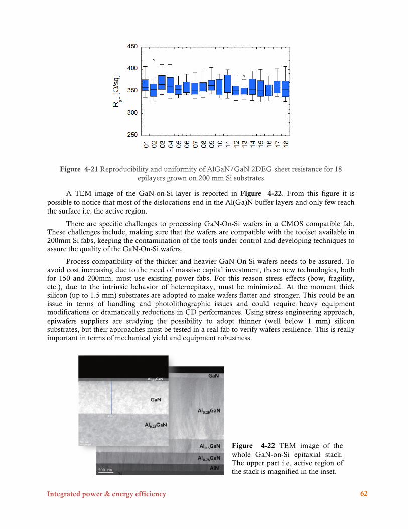
Integrated power & energy efficiency
62
Figure 4-21 Reproducibility and uniformity of AlGaN/GaN 2DEG sheet resistance for 18 epilayers grown on 200 mm Si substrates
A TEM image of the GaN-on-Si layer is reported in Figure 4-22. From this figure it is possible to notice that most of the dislocations end in the Al(Ga)N buffer layers and only few reach the surface i.e. the active region.
There are specific challenges to processing GaN-On-Si wafers in a CMOS compatible fab. These challenges include, making sure that the wafers are compatible with the toolset available in 200mm Si fabs, keeping the contamination of the tools under control and developing techniques to assure the quality of the GaN-On-Si wafers.
Process compatibility of the thicker and heavier GaN-On-Si wafers needs to be assured. To avoid cost increasing due to the need of massive capital investment, these new technologies, both for 150 and 200mm, must use existing power fabs. For this reason stress effects (bow, fragility, etc.), due to the intrinsic behavior of heteroepitaxy, must be minimized. At the moment thick silicon (up to 1.5 mm) substrates are adopted to make wafers flatter and stronger. This could be an issue in terms of handling and photolithographic issues and could require heavy equipment modifications or dramatically reductions in CD performances. Using stress engineering approach, epiwafers suppliers are studying the possibility to adopt thinner (well below 1 mm) silicon substrates, but their approaches must be tested in a real fab to verify wafers resilience. This is really important in terms of mechanical yield and equipment robustness.
Figure 4-22 TEM image of the whole GaN-on-Si epitaxial stack. The upper part i.e. active region of the stack is magnified in the inset.

Integrated power & energy efficiency
63
Therefore in [Marcon2012, DeJaeger2012] an assessment was made. It was shown that the thicker and heavier GaN-on-Si wafers could be processed on most production tools without significant hardware or process modifications. Occasionally, the robot speed of the wafer transport systems had to be lowered due to the larger inertia of thicker Si substrates.
In order to assure high quality devices, each wafer needs to be inspected for defects prior processing. CANDELA optical metrology systems from KLA Tencor are conventionally designed for transparent substrates and daily used in LED fabs to assess wafer quality. This system has been adapted for non-transparent wafers such as GaN-on-Si. [Marcon2012].
With the CANDELA system it is possible to obtain a wafer map of different types of defects, such as hexagonal defects (Figure 4-23a) and particles (Figure 4-23b). Eventually, these defect maps can be correlated with the final electrical device characterization map to identify detrimental defects.
Figure 4-23 SEM image of a a) hexagonal defect and b) particle
Since Ga is a p-type dopant for Si, one of the major concerns of processing GaN wafers in a CMOS fab is Ga contamination. One source of Ga contamination is the backside of the GaN-on-Si wafer since it is in contact with the chuck of the MOCVD epi tool. This is confirmed by TXRF (Total Reflection X-ray Fluorescence) analysis performed on bare Si wafers that were in contact with the chuck [Marcon2012].
To avoid Ga contamination, a HF/H2O2-based cleaning procedure was succesfully developed to be applied to the backside of GaN-on-Si wafers [Marcon2012]. The Ga contamination level of a Si wafer can be reduced to a level close to the detection limit of TXRF after using the proper cleaning steps [Marcon2012].
The second source of Ga contamination is related to etching steps. It was observed that etching tools got strongly contaminated when Ga-based layers were etched. Conventional F-containing cleaning recipes can form non-volatile GaFx species (i.e. GaFx is not volatile below 800°C), therefore in [Marcon2012] a new Cl2-based clean was developed that forms volatile GaCl3 at a much lower temperatures of ~ 200°C. This cleaning procedure effectively maintains the Ga contamination level well below the maximum allowed level for the whole monitored period
In conclusion, it can be said that there are currently no bottlenecks for the implementation and industrialization of large area GaN-On-Si wafers. Reports in the literature have shown that thick, crack free GaN epi layers can be grown on 200mm Si wafers, while keeping stress and bow under control. Furthermore, these wafers have been run through an industry compatible pilot line at Imec where no significant problems where found for processing these type of wafers. Tools can be adjusted to handle GaN-On-Si wafers through small and inexpensive modifications. Moreover, it has been proven that Ga contamination can be kept under control by using the proper cleans,
a) b)

Integrated power & energy efficiency
64
and etch recipes. This means that the GaN processes is compatible and can run in parallel with existing industry standard Si processes. Also QA assurance can be guaranteed on these wafers by using the proper non destructive metrology tools.
Advanced substrates In the III/V technologies, the design of a device structure requires the epitaxial growth of the
device layers stack. Usually the epitaxial growth is done on a bulk substrate of the same nature as the layer stack: bulk GaAs for GaAs related devices or bulk InP for InP related devices. This homoepitaxy allows an excellent quality of the epitaxial material.
The technologies for bulk GaN wafers exist today. It shows excellent crystal quality (dislocation density in the E4/cm² range) that could make a breakthrough in device performances but the wafer cost is not compatible with the market needs.
In order to be cost effective, other substrates have been used with a tradeoff between cost and performances, Depending on application, relevant substrates are Silicon, Sapphire and Silicon Carbide.
• GaN on Si is already available (several suppliers). It is the current substrate for Electronics power application.
• GaN on Sapphire (Al2O3) is settled as kind of standard in LED lighting business, competing with SiC.
• GaN on SiC is the reference substrate for electronic RF applications.
From today’s point of view, the advanced GaN substrates would compete with technologies like “GaN on Sapphire”, “GaN on SiC”, “GaN on Si” and/or “GaN on GaN”:
- GaN bulk substrate would obviously be the preferred substrate as it allows homoepitaxy, but cost and availability is currently unacceptable for high volume manufacturing of devices like LED’s or Power electronics.
- SiC substrate’s advantages are the acceptable CTE and lattice mismatched, the good thermal conductivity. Disadvantage are the cost and the availability in large diameter 150 mm and furthermore 200 mm.
- Sapphire substrate advantage is a CTE mismatch to GaN which lead to compressive strain in the GaN epitaxial device layer, the drawback of this material is the lattice mismatch leading to the difficulty of growing low defect GaN and low scalability towards larger dimension and the related cost. The low thermal conductivity of sapphire is also an issue and lead to use epitaxy lift off of the final device for some applications.
- Silicon substrate advantages are a better compatibility with standard process lines, low price (high availability) and large wafer diameters (up to 200mm – as 111 wafers are not available in 300mm). Furthermore, silicon has higher thermal conductivity compared with sapphire, and is easily thinnable to maximize thermal conductivity especially important in LEDs. However, disadvantages are directly linked to the hetero-epitaxy: the CTE mismatch (vs GaN) which leads to tensile strain in the GaN epitaxial layer and lattice mismatch (vs GaN); both leading to the need of thick and complex buffer and difficulties to grow crack free GaN layer with low defectivity and low bow. In any case, the thickness of the GaN active layers remains limited to some µm. The crystal quality and epitaxial layer thickness impacts reliability of devices and the maximum voltage operation. The BOW degradation impacts strongly fabrication yield and could be a stopper for further scalability to 200mm and beyond. Thus the level of performance might not be sufficient for the market needs. The complexity and CTE
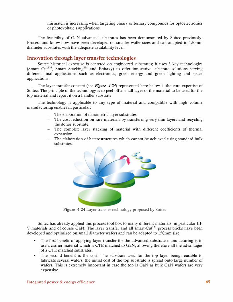
Integrated power & energy efficiency
65
mismatch is increasing when targeting binary or ternary compounds for optoelectronics or photovoltaic’s applications.
The feasibility of GaN advanced substrates has been demonstrated by Soitec previously.
Process and know-how have been developed on smaller wafer sizes and can adapted to 150mm diameter substrates with the adequate availability level.
Innovation through layer transfer technologies Soitec historical expertise is centered on engineered substrates; it uses 3 key technologies
(Smart CutTM, Smart StackingTM and Epitaxy) to offer innovative substrate solutions serving different final applications such as electronics, green energy and green lighting and space applications.
The layer transfer concept (see Figure 4-24) represented here below is the core expertise of Soitec. The principle of the technology is to peel-off a small layer of the material to be used for the top material and report it on a handler substrate.
The technology is applicable to any type of material and compatible with high volume manufacturing enables in particular:
– The elaboration of nanometric layer substrates, – The cost reduction on rare materials by transferring very thin layers and recycling
the donor substrate, – The complex layer stacking of material with different coefficients of thermal
expansion, – The elaboration of heterostructures which cannot be achieved using standard bulk
substrates.
Figure 4-24 Layer transfer technology proposed by Soitec
Soitec has already applied this process tool box to many different materials, in particular III-
V materials and of course GaN. The layer transfer and all smart-CutTM process bricks have been developed and optimized on small diameter wafers and can be adapted to 150mm size.
• The first benefit of applying layer transfer for the advanced substrate manufacturing is to use a carrier material which is CTE matched to GaN, allowing therefore all the advantages of a CTE matched substrates.
• The second benefit is the cost. The substrate used for the top layer being reusable to fabricate several wafers, the initial cost of the top substrate is spread onto large number of wafers. This is extremely important in case the top is GaN as bulk GaN wafers are very expensive.

Integrated power & energy efficiency
66
• The third benefit is the preservation of the initial substrate (GaN Raw material) crystal quality by the Smart Cut™ technology. Thanks to that, a GaN wafer with dislocation density of 10E4/cm² at compatible cost is possible.
• Finally the wafer deformation can be minimized by engineering the handle substrate to match the BOW deformation requirement. The choice for handle substrate is opened to material compatible with the thermal expansion coefficient of the GaN material.
Conclusions
GaN and SiC materials are already widely used in the power RF applications. There still remain many barriers for broader adoption of these materials in energy conversion applications, such as material cost and availability, quality, wafer diameter scalability and a well-established industrial supply chain. There is also room for innovations in the advanced substrates technologies. References [ACS, 2012] “SiC Systems” Corp presentation, Angel Capital Summit, 22sdMarch2012 [Bridgelux, 2011] Bridgelux, Aug 9, 2011, Bridgelux announces new breakthrough in GaN-on-
Silicon technology for solid-state lighting (http://bridgelux.com/media-center/press-releases/bridgelux-announces-new-breakthrough-in-gan-on-silicon-technology-for-solid-state-lighting/)
[Cheng, 2012] K. Cheng et al., “AlGaN/GaN/AlGaN Double Heterostructures Grown on 200mm Silicon (111) Substrates with High Electron Mobility”, Appl. Phys. Express, Vol. 5, p. 011002 (2012).
[De Jarger, 2012] B. De Jaeger et al., “Au-free CMOS-compatible AlGaN/GaN HEMT processing on 200 mm Si substrates”, proceeding of ISPSD, pp. 49-52, 2012.
[ElectroIQ, 2012] ElectroIQ, Jun 12, 2012, Lattice Power ramps high-power GaN-on-Si LED production (http://www.electroiq.com/articles/sst/2012/06/lattice-power-ramps-high-power-gan-on-si-led-production.html)
[EP, 2011] Electronic Products, Jan 2011, Enhancement-mode GaN power transistor points to the look of the future,
[EPC2011] http://www2.electronicproducts.com/ [GSA, 2012] “Unleashing Growth in Wide Bandgap : The upcoming disruptions in power
electronics”, GSA Semiconductor Leaders Forum Taiwan, McKinsey&Company [IMS, 2012] “The world market for silicon carbide & gallium nitride power semiconductors – 2012
edition”, IMS Research, 2012 [Marcon, 2012] D. Marcon et al., “Manufacturing challenges of GaN-on-Si HEMTs in a 200mm
CMOS fab”, ISSM 2012 [Merchant, 1991] S. Merchant, E. Arnold; H. Baumgart, S. Mukherjee, H. Pein, R. Pinker,
“Realisation of high breakdown voltage (>700V) in thin SOI devices”, ISPSD’91, pp 31-35, 991.
[Nitronex, 2012] Nitronex Corporate Fact Sheet - 2Fwww.nitronex.com [Van Hove, 2012] M. Van Hove et al., “CMOS Process-Compatible High-Power Low-Leakage
AlGaN/GaN MISHEMT on Silicon”, IEEE Electron Device Lett., Vol. 33, No. 05, p. 667 (2012).
[Yasuhara, 1991] N. Yasuhara, A. Nakagawa, K. Furukawa, “SOI devices structures implementing 650V high voltage output devices on VLSIs”, Electron Devices Meeting, pp 141-144, Dec 1991.
[Yole, 2012] “SiC Market, 2010-2020: 10 year market projection”, Yole, 3rdnov2012 (Yole public advertising document for the report)

Integrated power & energy efficiency
67
Simulation of Power devices
Jürgen Lorenz (Fraunhofer IISB) With the contribution of:
Wolfgang Dettmann (Infineon) Angelo Magrì (STMicroelectronics) Peter Moens (ONsemiconductor) Joachim Pelka, (Fraunhofer VµE) Jan Sonsky (NXP)
Abstract
Technology Computer Aided Design (TCAD) has during the last decades developed into a key tool to support the development and optimization of semiconductor technologies, devices and circuits. Its scope extends from the simulation of process equipment through simulation of processes and devices to the simulation of circuits and systems. It is based on a thorough understanding of the physical effects involved at all these levels, the extraction of the required physical parameters, and the implementation of the models developed into simulation tools which enable an efficient and predictive simulation.
The International Technology Roadmap for Semiconductors ITRS among others also contains a chapter on Modeling and Simulation. This chapter gives an estimate of about one third for the reduction of development times and costs for best practice cases in nanoelectronics [ITRS2013]. This should also be the aim for power electronics.
Because the core of simulation comprises quantitative physical understanding and efficient algorithms, leading-edge simulation tools are mostly quite generic and may be used for a large variety of processes and devices. The range of such applications spans from aggressively scaled memory and logic devices to RF and power devices. In parallel to new device architectures being suggested and explored, simulation tools have developed from relatively simple one-dimensional tools in the 1970s [Antoniades1979, Ryssel1980, Oldham1979] to two-dimensional one in the 80s and 90s (e.g. [Law1988]) to the sophisticated three-dimensional tools, which are currently needed for many applications. In consequence, the generation and adaptation of suitable numerical meshes has become a key challenge for simulation, which is still not fully solved in spite of the considerable progress having been achieved (see e.g. the subchapter on “Numerical Methods and Interoperability of Tools” in the “Modeling and Simulation” chapter of the ITRS [ITRS2013]). Besides this, power electronic applications are based on specific circuit architectures and devices, and partly use specific device fabrication technologies not found in other areas. Moreover, some effects which are also existing in other applications are much more important in power devices due to the large power densities involved.
The market for TCAD tools is currently dominated by some large suppliers mainly based in the US, like Synopsys [Synopsys2013] and Silvaco [Silvaco2013], which offer a variety of integrated tools, covering most of the area of TCAD. Besides this, research institutions and smaller companies provide some alternative pro-grams and especially leading-edge solutions with particular advantages in specific areas (e.g. lithography simulation, see e.g. [Prolith2013], [Litho2013]). Generally, in the last decade, the leading TCAD vendors have strengthened their position among others by buying and integrating smaller innovative competitors. For

Integrated power & energy efficiency
68
semiconductor industry, the disadvantage is the existence of an oligopoly or partly duopoly of suppliers, which leaves the industry with little alternatives.
In this chapter, the main additional features needed for the simulation of power devices and their fabrication, as well as the state-of-the art in these areas, are summarized. Important additional requirements are identified in the areas of process, device and circuit simulation. As part of this, also the numerical algorithms are faced with additional challenges.
Process Simulation During the last three decades, the models used in process simulation have evolved from
rather simple phenomenological approaches to partly quite sophisticated physically based models which are at least to some extent and in some areas of application predictive. The most critical element for the research work on such models has been the design and conduction of dedicated experiments, which are suitable to separate and understand the physical processes occurring, to set up model equations describing these effects, and to extract the required model parameters. Due to the diversity of expertizes and of experimental facilities needed, a close cooperation between key players from industry and research is needed especially for such work on model development. Very good examples for the success of this cooperative approach are European projects like ATOMICS [Atomics2009], finished in 2009. Figure 4-25 shows the comparison of simulation results to SIMS measurements for combined spike and flash annealing. A similar cooperative approach should also be adopted for improvements needed especially for the simulation of power devices. Whereas industrial applications largely rely on commercial programs from US-based software houses like Synopsys or Silvaco, current enhancements of physical models are frequently first developed outside such tools, often using their open model interfaces and scripting languages
Figure 4-25 Comparison of simulation results to SIMS measurements on a sample implanted with an energy of 1 keV and a dose of 1015 cm-2 after a spike anneal at 1000°C followed by a flash anneal at 1300° [Martinez2008]
Various extensions and adaptations are needed for application to power devices. This starts from the use of complementary dopant species such as aluminum, which requires model parameters to be newly extracted, and partly also the model equations themselves. A similar but even larger modification results from the use of other materials instead of silicon: For silicon carbide (SiC), as an example, diffusion is about negligible, whereas dopant activation is the major problem and must therefore be accurately modeled: Presently, there is no complete picture available for the implantation and annealing in SiC. The properties of SiC devices are strongly influenced by defects like the generation of traps at the interface between SiC and oxide, basal plane dislocations and their glide during current flow, or recombination centers in epitaxial layers.

Integrated power & energy efficiency
69
Furthermore, additional specific process steps are used for power devices and need to be covered in simulation. Typical examples are lifetime engineering in silicon by the diffusion of gold or platinum, or the implantation of hydrogen or helium, as well as the etching of deep trenches required by advanced power semiconductor device architectures such as CoolMOS/superjunction transistors.
Since several years the need for three-dimensional simulation has developed in nanoelectronics, because aggressive scaling increasingly requests three-dimensional device structures such as the well-known FinFET transistors. This has raised large challenges in the development of tools both for process and device simulation, in terms of surface and bulk meshing, simulation of geometries developing during the device fabrication process, and generally efficiency of simulation tools in terms of memory usage and computation time, in order to deal with the large increase of the number of mesh points when going from two- to three dimensional simulation. Nanoelectronics applications have been the driving force for this development, e.g. in the cooperative EC projects like MAGIC_FEAT [Magic2013], and led to considerable progress, which among others shows up in commercial simulation tools e.g. from Synopsys and Silvaco. Figure 4-26 shows an example for geometry, mesh and doping distribution of a 21 nm FinFET NMOS transistor.
Figure 4-26 Example for geometry, arsenic distribution and mesh of a 21 nm NMOS transistor, simulated with Sentaurus Process from Synopsys
However, major improvements and extensions are still needed, also to cope with the requirements of advanced power devices such as CoolMOS or superjunction. The challenge of providing versatile, efficient and user-friendly automatic meshing tools especially for three-dimensional simulation is still only partly met. The general target is to achieve a sufficient accuracy in the solution of the discretized model equations whereas at the same time limiting the effort in terms of memory requirements and computation times to acceptable values. An absolutely mandatory requirement for each meshing tool is an appropriate and automatic adaptation of the meshes to varying quantities in the bulk, e.g. steep dopant or carrier profiles. Here, mesh refinement by insertion of additional mesh points is the easier problem, whereas mesh un-refinement in areas where mesh nodes have become obsolete is quite difficult to implement in some meshing concepts. Specific to process simulation is the requirement to first appropriately discretize surfaces and interfaces, which are frequently highly non-planar and for some process steps also time-dependent. Such surface discretization is indispensable to accurately describe the development of device geometries during processing. The other specific meshing requirement is the need to suitably combine bulk meshes with these surface meshes, especially for the three-dimensional simulation of oxidation. Whereas considerable effort has been spent during the last years on the development of meshing tools, current tools still need to be enhanced in various
Integrated power & energy efficiency
70
respects. This is especially true for current and upcoming highly three-dimensional device architectures, such as FinFETs in nanoelectronics or CoolMOS/superjunction power devices.
Besides full 3D process simulations there is also the industrial need to perform 3D emulation of power devices, which is a helpful instrument for the design of very big discrete devices. As an example, SEMulator3D (Coventor) [Coventor2013] emulates physical process steps using parameterized geometric modeling algorithms. The SEMulator3D modeling engine is based on unique voxel modeling technology. Voxels are like 3D pixels filled with one or more materials (similar to the RGB colors in a pixel) that enable SEMulator3D to model arbitrary geometric shapes. Starting from a GDSII input file and a brief process flow, SEMulator3D builds a 3D wide structure with a very low time consuming. Although they do not allow for predictive simulation, tools like SEMulator3D provide a “Virtual FAB” which permits industry to assess layouts and process bugs.
In summary, in order to make process simulation as useful for the development and fabrication of power devices as for that of CMOS for memory or logic applications, new, extended or adapted physical models must be developed and be made available in the standard tools used in industry. This requires significant cooperative efforts between the power semiconductor industry and research. A major non-scientific problem is the lack of major software vendors based in Europe and, in turn, the need to organize a suitable cooperation with US-based software houses.
Device Simulation Also in device simulation, the large progress obtained during the last decades has mainly
been promoted by the requirements raised by aggressively scaled nanoelectronic transistors, which led to several elaborated methods e.g. based on the Boltzmann equation for carrier transport and for quantum-mechanical effects. In parallel to this, the need for three-dimensional device simulation became essential, and has in the meantime led to several three-dimensional device simulation tools, e.g. the commercial ones from Synopsys and Silvaco. Similar to process simulation, appropriate adaptive meshing and computational efficiency have been key challenges. Whereas moving surfaces and interfaces have been the specific problem for process simulation, in case of device simulation the quality of the mesh elements (“Delaunay criterion”) is even more important to enable correct and efficient simulations, in order to meet the requirements of the Scharfetter-Gummel [Scharfetter1969] stabilization scheme which is essential for device simulation. Again, in spite of the progress obtained so far, considerable enhancements are still needed. For power devices, meshes and algorithms must be especially adapted to accurately simulate the high voltages and currents occurring during switching.
Based on the remarkable progress obtained in the development and implementation of physical models for aggressively scaled nanoelectronic devices, several effects must be modeled which gain additional importance for power devices. This includes the impact of traps on device performance, carrier velocity saturation, impact ionization, current filamentation, mobility degradation, the JFET effect, and non-linear charge storage effects. Due to the large electrical currents in power devices, the formation of suitable contacts is a major issue and needs to be addressed: E.g. the formation of contacts on SiC is still a problem due to its large bandgap, and existing models for Schottky contacts are only valid for even surfaces.
Even more than for scaled nanoelectronic devices, electro-thermo-mechanical interactions within the active device and with its contacts and packages critically influences device performance and reliability and must therefore be simulated. Figure 4-27 shows an example for the self-heating of a bulk NMOSFET following specifications for 2015 from the 2011 ITRS. Generally, models must be extended and adapted to allow the simulation of devices based on semiconducting materials such as SiC, GaN, and their alloys. Especially for SiC MOSFETS, the impact of carbon clusters, nitrogen and of defects located close to the SiC surface must be modeled. Figure 4-28 shows exemplarily the impact of these defects on the transfer characteristics of SiC-MOSFETs.

Integrated power & energy efficiency
71
The variant of simulation without taking the surface related defects into account differs very much from the measurements and only simulations accounting for these defects are capable to reproduce the measurements. The effect of the surface related defects is strongly influenced by several technological options and must be characterized for different variants of transistor processing.
Figure 4-27 Temperature distribution due to self-heating in a 17 nm SOI silicon NMOSFET in the on-state [Burenkov2011], simulated with SENTAURUS-Device from Synopsys
Figure 4-28 Transfer characteristics of a 4H-SiC MOSFET at drain voltage of 0.1 V simulated with the impact of the defects on the interface between the SiC and the gate oxide (a) and ideal interface (b) in comparison with measurements (c - dots)
Among others there are several open issues concerning the simulation of the physical effects at the AlGaN/GaN interface. For some advanced power device architectures such as CoolMOS/superjunction, charge carrier lifetimes are more important than in conventional CMOS. Requirements for the accuracy of impact ionization models are higher than in the case of standard CMOS because the avalanche process must be controlled in power devices. The simulation of radiation effects is insufficient in current commercial device simulators and needs to be improved to predict the impact on the reliability of power devices, especially by removing the limitations of current meshing tools, as mentioned above.
Mixed-Mode simulations Due to more and more complex structures, designers need a wide range of static and
dynamic simulations to predict the overall circuit behavior. To do that, particularly when suitable

Integrated power & energy efficiency
72
compact models are not available, more complex simulations are required involving both device structure and circuit layout.
Mixed-mode simulations satisfy this requirement by solving the semiconductor equations if needed for several devices at the same time and for boundary conditions defined by the external circuitry comprising active and passive devices. Circuitry information is typically provided in a SPICE-like netlist format. Particularly for power semiconductors, a self-consistent solution of heat generation and dissipation together with the semiconductor equations will be necessary. With these considerations, the mixed-mode simulations are normally addressed to replicate standard test procedures (turn-on/off, UIS, gate charge, reverse recovery …) but also to assist in the circuit-device co-design for application-oriented purposes. Power losses in high-frequency converters (>1MHz), for instance, represent an interesting field of study due to the predominance of the complex transient mechanism. In PowerMOSFETs, as an example, an accurate prediction of the intrinsic parasitic capacities (CISS, COSS, CRSS,-input, output and reverse transfer capacitance, respectively) play an important role during the switch-on/off process. Note that, in general, CISS, COSS, CRSS are non-linear and, sometimes, their VDS dependence is difficult to fit with a simple exponential or inverse proportional decay (normally implemented in SPICE models). Moreover, if the PowerMOSFET acts as synchronous rectifier, the behavior during the ID-VD third quadrant and the reverse recovery of the parasitic diode become relevant. The previous mechanisms become complicated to evaluate by simple SPICE models when the current is diverted through different paths, namely channel and parasitic transistor. Accounting for the device physics and structural details, mixed-mode simulations allow a significant gain in precision when predicting circuit efficiencies but it also provides physical insight in problems related to voltage/current overshoots or cross conduction among others. On the other hand the computational time is generally superior to the one required by pure SPICE simulations. The latest issue could be partially alleviated by defining simulation strategies, which combine stationary with transient simulations, in a periodic behavior, but also by simplifying some of the circuit blocks.
Circuit Simulation Circuit simulators such as SPICE and its commercial variants like HSPICE and PSPICE
employ a text netlist consisting of circuit elements such as transistors, resistors, capacitative and inductive elements, and derive from these algebraic differential equations to be solved. In some cases semiconductor companies also derived their proprietary variants, such as TITAN by Infineon. Besides the efficiency and performance of the algorithms used to solve these equations, the quality of the results obtained by circuit simulation depends on the physical models used to describe the circuit elements, e.g. using the widely spread BSIM models for MOS transistors. An industrial association called Compact Modeling Council [CMC2013] was established to review newly suggested models and in this way give guidelines for model development and application. It is important to point out that here “model” has a completely different meaning compared with process and device simulation, where they are mostly based on partial differential equations discretized on meshes in space and time, plus equations for the basic physical expressions and parameters used, such as diffusion coefficients or carrier mobilities. In contrast to this, circuit models are based on simple analytical formulas describing the electrical behavior of the circuit elements, and employ model parameters such as threshold voltage, subthreshold slope, saturation current, etc. These parameters can be extracted either from experiment or from numerical device simulations.
Extensions needed for the application of circuit simulation to power electronics consist especially of the development and extraction of the compact models which are needed to describe circuit elements specific for power electronics. This includes especially power transistors such as CoolMOS / superjunctions. Furthermore, it is important to note that thermal effects are even more important in power electronics than for scaled More Moore devices, which raises the requirement for suitable extensions of the compact models and the circuit simulators.

Integrated power & energy efficiency
73
Conclusion It is common understanding in industry and research that TCAD simulations are an
invaluable mean to investigate and optimize new processes and devices and to identify and analyze factors that cause parametric yield loss in manufacturing, when new processes, new device architectures and/or new materials are introduced. Appropriate use of TCAD strongly contributes to the reduction of development times and costs, and to increasing product yield on a wide range of technologies. This very well justifies investment in the development of the models and tools needed to carry out the required simulation studies. Especially, new, extended or adapted physical models must be developed and be made available in the standard tools used in industry, in order to cope with the requirements of specific materials, processes and architectures used for power devices. This requires significant cooperative efforts between the power semiconductor industry and research, which can best be carried out in cooperative projects such as CATRENE.
References [Antoniades1979] D.A. Antoniades, R.W. Dutton, “Models for Computer Simulation of
Complete IC Fabrication Processes”, IEEE Trans. Electron Devices, vol. 26, pp. 490-500, Apr. 1979.
[Atomics2009] EC FP6 project 027152 ATOMICS –http://cordis.europa.eu/projects/rcn/80668_en.html
[Burenkov2011] Alex Burenkov, Jürgen Lorenz, “Self-Heating Effects in Nano-Scaled MOSFETs and Thermal-Aware Compact Models”, in Proc. of the 17th International Workshop on Thermal investigations of ICs and Systems, THERMINIC 2011, 27-29 September 2011, Paris, France.
[CMC2013] See http://www.geia.org/CMC-Introduction [Coventor2013] See http://www.coventor.com/products/semulator3d/ (latest access at Jan. 3,
2013) [ITRS2011] The International Technology Roadmap for Semiconductors, 2011 issue: Modeling
and Simulation chapter, table MS3, see http://www.itrs.net/Links/2011ITRS/Home2011.htm
[Law1988] M.E. Law and R.W. Dutton, “Verification of Analytic Point Defect Models using SUPREM-IV,” IEEE Transactions on Computer Aided Design, 7(2), p. 181–190 1988.
[Litho2013] Dr.LiTHO - see http://www.drlitho.com/cms/website.php (latest access at Jan. 3, 2013)
[Magic2012] EC FP5 project 11433 MAGIC_FEAT – Meshes and Global Integration for Semiconductor Front-End Simulation, Start: 1/1/2000 - End: 12/31/2002
[Martinez2008] A. Martinez-Limia, P. Pichler, C. Steen, S. Paul, W. Lerch, “Modeling and Simulation of Advanced Annealing Processes”, Materials Science Forums Vols. 573-574 (2008), pp. 279-293, online at http://www.scientific.net/MSF.573-574.279
[Oldham1979] W. Oldham, S. Nandgaonkar, A. Neureuther and M. O’Toole, “A general simulator for VLSI lithography and etching processes: Part I – Applications to projection lithography”, IEEE Trans. Electron Devices, vol. 26, pp. 717-722, Apr. 1979.
[Prolith2013] PROLITH - see http://www.kla-tencor.com/lithography-modeling/chip-prolith.html
[Ryssel1980] H. Ryssel, K. Haberger, K. Hoffmann, G. Prinke, R. Dümcke, A. Sachs, “Simulation of Doping Processes”, IEEE Trans. Electron Devices, vol. 27, pp. 1484-1492, Aug. 1980.
[Scharfetter1969] D.L Scharfetter and H.K. Gummel, “Large-Signal Analysis of a Silicon Read Diode Oscillator,” IEEE Trans. Electron Devices, vol. 16, pp. 64–77, January 1969.
[Silvaco2013] See http://www.silvaco.com/products/tcad/index.html (latest access at Jan. 3. 2013)
[Synopsys2013] See http://www.synopsys.com/Tools/TCAD/Pages/default.aspx
Integrated power & energy efficiency
74
Reliability issues in Si-Power devices
Peter Moens (ONSemiconductor) With the contribution of:
Filip Bauwens (ONSemiconductor) Angelo Magrì (STMicroelectronics) Jan Sonsky (NXP)
Abstract
This section provides an overview of the most relevant reliability issues in Si based power devices (diodes, MOSFETs, IGBTs,…). Although Si technologies are well established and have proven long term reliability, some important reliability issues deserve further study and improvement, especially for high voltage devices.
As many silicon-based power devices are MOS-type (power MOSFETs, IGBTs etc), and as power MOS devices have a large Si area (several mm2 up to a few cm2), both intrinsic as well as extrinsic reliability of the dielectric is important. The former is especially true for high temperature operation, since power MOSFETs can reach high local junction temperatures, leading to an accelerated dielectric degradation. The latter is defect driven, and scales with the device area. On top, many novel Power MOSFETs and IGBTs have trench gates or trench super-junctions, so that oxide and interface quality on trench sidewalls is important.
To account for the need of higher voltages in the Si-Power devices, very often as in the case of IGBTs and diodes, the Silicon background doping is severely lowered. This puts more constraints on the power limitations since a low current density in the device during switching can already destroy its avalanche ruggedness. This effect is well understood and some tricks exist to overcome the problem, e.g. introduction of buffer layers, injection of minority carriers, etc. However this always comes at a cost and thus avoiding the sensitivity towards destruction by low current density switching is favored. Materials with higher maximum electric field capability compared to Silicon are preferred in that respect.
Additional reliability issues mainly include passivation integrity failures, due to the lack of sufficient screening of the mobile charges in the mold compound from the lowly doped epi layers in the device termination (HTRB and H3TRB testing), cracking of the passivation layers, and device parameters shifting upon avalanche conditions (repetitive UIS testing)
Overview of Power MOSFET reliability and qualification testing
Table 4-2 overviews the standard extrinsic reliability and qualification testing for Si-based Power MOSFETs, for both industrial, automotive and military qualification.
Table 4-3 overviews the standard intrinsic reliability testing for Si-based power MOSFETs
for platform qualification. Both tables are compliant with the general Si Power device qualification spec AEC-Q101.
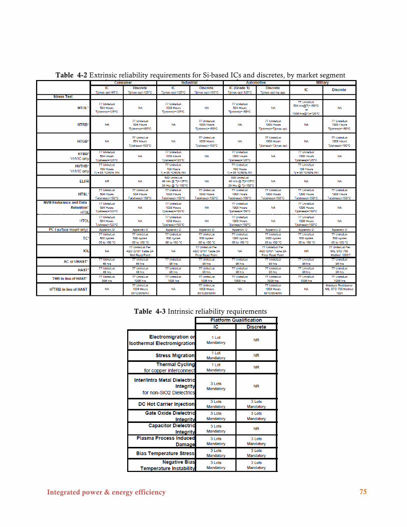
Integrated power & energy efficiency
75
Table 4-2 Extrinsic reliability requirements for Si-based ICs and discretes, by market segment
Table 4-3 Intrinsic reliability requirements
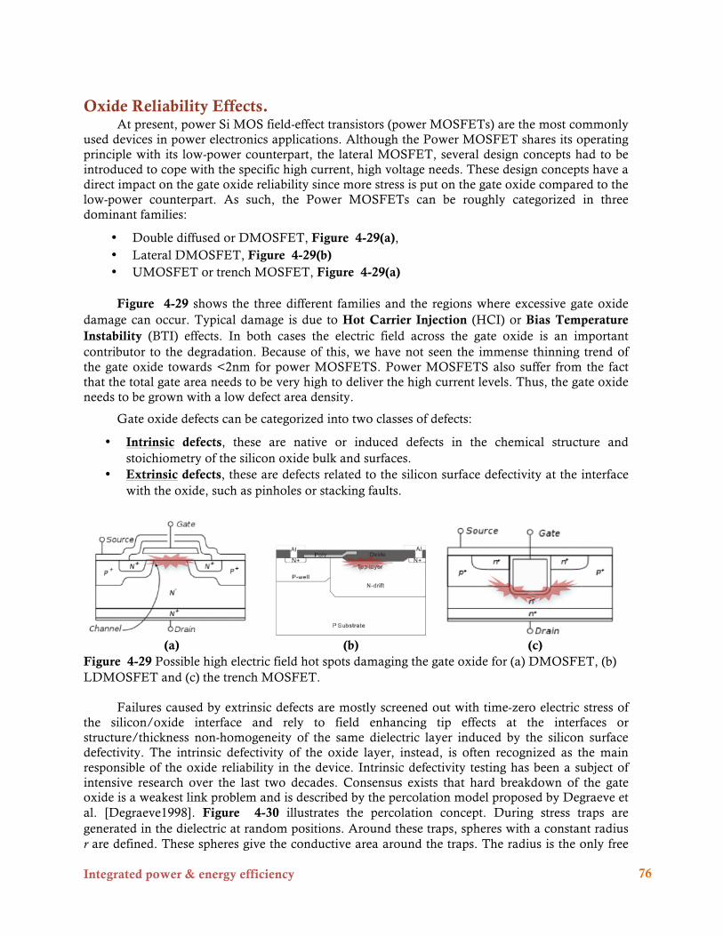
Integrated power & energy efficiency
76
Oxide Reliability Effects. At present, power Si MOS field-effect transistors (power MOSFETs) are the most commonly
used devices in power electronics applications. Although the Power MOSFET shares its operating principle with its low-power counterpart, the lateral MOSFET, several design concepts had to be introduced to cope with the specific high current, high voltage needs. These design concepts have a direct impact on the gate oxide reliability since more stress is put on the gate oxide compared to the low-power counterpart. As such, the Power MOSFETs can be roughly categorized in three dominant families:
• Double diffused or DMOSFET, Figure 4-29(a), • Lateral DMOSFET, Figure 4-29(b) • UMOSFET or trench MOSFET, Figure 4-29(a)
Figure 4-29 shows the three different families and the regions where excessive gate oxide
damage can occur. Typical damage is due to Hot Carrier Injection (HCI) or Bias Temperature Instability (BTI) effects. In both cases the electric field across the gate oxide is an important contributor to the degradation. Because of this, we have not seen the immense thinning trend of the gate oxide towards <2nm for power MOSFETS. Power MOSFETS also suffer from the fact that the total gate area needs to be very high to deliver the high current levels. Thus, the gate oxide needs to be grown with a low defect area density.
Gate oxide defects can be categorized into two classes of defects:
• Intrinsic defects, these are native or induced defects in the chemical structure and stoichiometry of the silicon oxide bulk and surfaces.
• Extrinsic defects, these are defects related to the silicon surface defectivity at the interface with the oxide, such as pinholes or stacking faults.
(a) (b) (c)
Figure 4-29 Possible high electric field hot spots damaging the gate oxide for (a) DMOSFET, (b) LDMOSFET and (c) the trench MOSFET.
Failures caused by extrinsic defects are mostly screened out with time-zero electric stress of the silicon/oxide interface and rely to field enhancing tip effects at the interfaces or structure/thickness non-homogeneity of the same dielectric layer induced by the silicon surface defectivity. The intrinsic defectivity of the oxide layer, instead, is often recognized as the main responsible of the oxide reliability in the device. Intrinsic defectivity testing has been a subject of intensive research over the last two decades. Consensus exists that hard breakdown of the gate oxide is a weakest link problem and is described by the percolation model proposed by Degraeve et al. [Degraeve1998]. Figure 4-30 illustrates the percolation concept. During stress traps are generated in the dielectric at random positions. Around these traps, spheres with a constant radius r are defined. These spheres give the conductive area around the traps. The radius is the only free
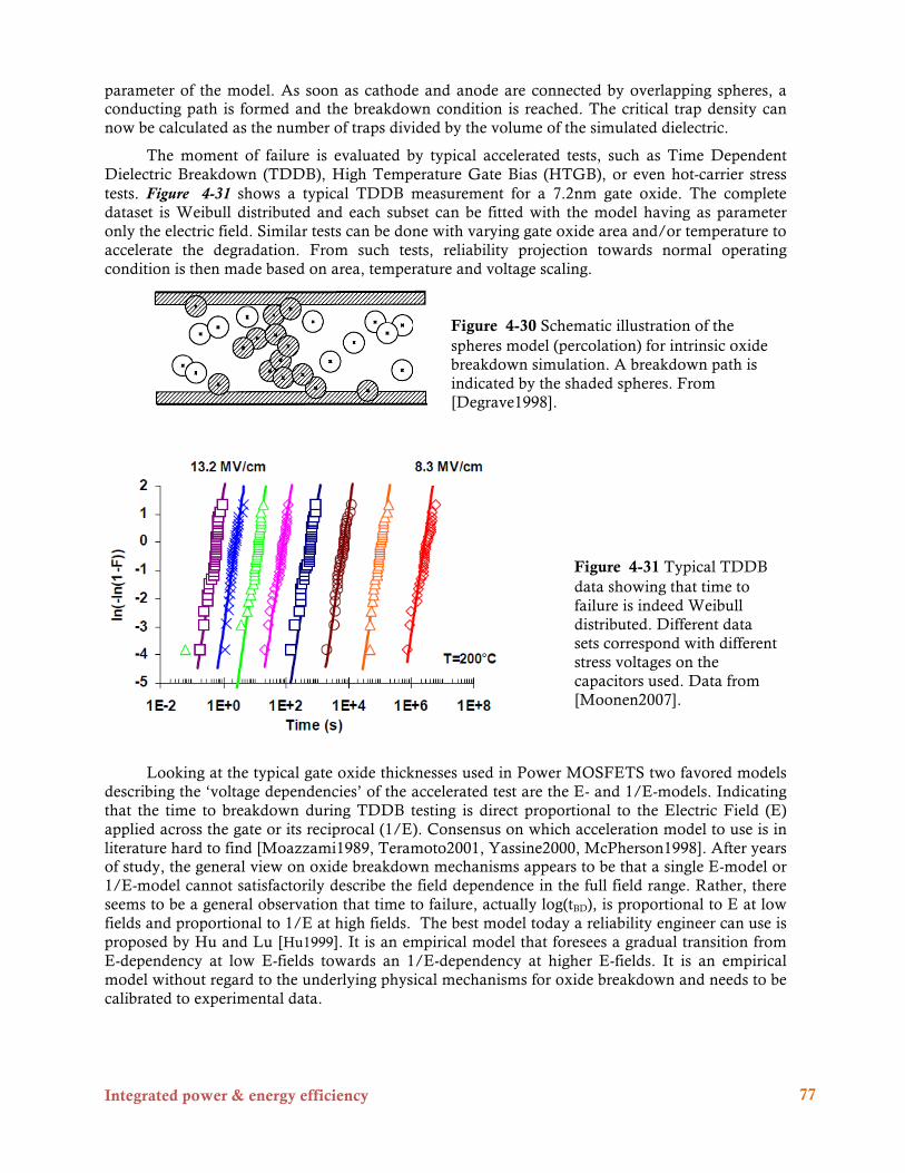
Integrated power & energy efficiency
77
parameter of the model. As soon as cathode and anode are connected by overlapping spheres, a conducting path is formed and the breakdown condition is reached. The critical trap density can now be calculated as the number of traps divided by the volume of the simulated dielectric.
The moment of failure is evaluated by typical accelerated tests, such as Time Dependent Dielectric Breakdown (TDDB), High Temperature Gate Bias (HTGB), or even hot-carrier stress tests. Figure 4-31 shows a typical TDDB measurement for a 7.2nm gate oxide. The complete dataset is Weibull distributed and each subset can be fitted with the model having as parameter only the electric field. Similar tests can be done with varying gate oxide area and/or temperature to accelerate the degradation. From such tests, reliability projection towards normal operating condition is then made based on area, temperature and voltage scaling.
Figure 4-30 Schematic illustration of the spheres model (percolation) for intrinsic oxide breakdown simulation. A breakdown path is indicated by the shaded spheres. From [Degrave1998].
Figure 4-31 Typical TDDB data showing that time to failure is indeed Weibull distributed. Different data sets correspond with different stress voltages on the capacitors used. Data from [Moonen2007].
Looking at the typical gate oxide thicknesses used in Power MOSFETS two favored models describing the ‘voltage dependencies’ of the accelerated test are the E- and 1/E-models. Indicating that the time to breakdown during TDDB testing is direct proportional to the Electric Field (E) applied across the gate or its reciprocal (1/E). Consensus on which acceleration model to use is in literature hard to find [Moazzami1989, Teramoto2001, Yassine2000, McPherson1998]. After years of study, the general view on oxide breakdown mechanisms appears to be that a single E-model or 1/E-model cannot satisfactorily describe the field dependence in the full field range. Rather, there seems to be a general observation that time to failure, actually log(tBD), is proportional to E at low fields and proportional to 1/E at high fields. The best model today a reliability engineer can use is proposed by Hu and Lu [Hu1999]. It is an empirical model that foresees a gradual transition from E-dependency at low E-fields towards an 1/E-dependency at higher E-fields. It is an empirical model without regard to the underlying physical mechanisms for oxide breakdown and needs to be calibrated to experimental data.

Integrated power & energy efficiency
78
21
21
BDBD
BDBDBDUnified tt
ttt+
=
Where tBDUnified is the time to breakdown, tBD1 is fitted by a single linear-E relation in the low field regime (tBD1=t1exp(-γEox), see Figure 4-32(a) and tBD2 is fitted by a single 1/E-relation in the high field regime ( tBD2=t2exp(G/Eox), see Figure 4-32(b). Finally the unified TDDB model is illustrated in Figure 4-32(c), where the tBD shows a linear E dependence in low field region and 1/E dependence in high field region, and a smooth transition between the two mechanisms.
Even today, the calibration towards low E-fields is still problematic since it involves time-consuming stressing experiments. Furthermore it is debatable if these lowest feasible accelerated stress conditions can be used to predict reliability at normal operating conditions since even the lowest feasible accelerated stress conditions rely on the fact that some tunneling current needs to be present to accelerate the aging effect of the oxide. This condition is different from normal operating conditions where no measurable tunneling current is present.
(a) (b)
(c) Figure 4-32: (a) TDDB data from different sources shows E-field dependency at low E-fields. (b) 1/E-field dependency at high E-fields for different technologies. (c) the Unified TDDB model showing a good fit over the complete E-field range. Data from [Hu1999 and references herein].
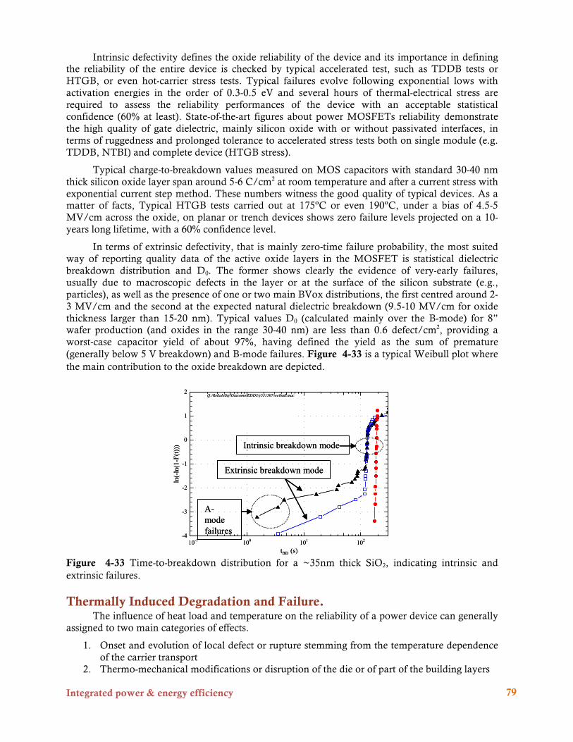
Integrated power & energy efficiency
79
Intrinsic defectivity defines the oxide reliability of the device and its importance in defining the reliability of the entire device is checked by typical accelerated test, such as TDDB tests or HTGB, or even hot-carrier stress tests. Typical failures evolve following exponential lows with activation energies in the order of 0.3-0.5 eV and several hours of thermal-electrical stress are required to assess the reliability performances of the device with an acceptable statistical confidence (60% at least). State-of-the-art figures about power MOSFETs reliability demonstrate the high quality of gate dielectric, mainly silicon oxide with or without passivated interfaces, in terms of ruggedness and prolonged tolerance to accelerated stress tests both on single module (e.g. TDDB, NTBI) and complete device (HTGB stress).
Typical charge-to-breakdown values measured on MOS capacitors with standard 30-40 nm thick silicon oxide layer span around 5-6 C/cm2 at room temperature and after a current stress with exponential current step method. These numbers witness the good quality of typical devices. As a matter of facts, Typical HTGB tests carried out at 175ºC or even 190ºC, under a bias of 4.5-5 MV/cm across the oxide, on planar or trench devices shows zero failure levels projected on a 10-years long lifetime, with a 60% confidence level.
In terms of extrinsic defectivity, that is mainly zero-time failure probability, the most suited way of reporting quality data of the active oxide layers in the MOSFET is statistical dielectric breakdown distribution and D0. The former shows clearly the evidence of very-early failures, usually due to macroscopic defects in the layer or at the surface of the silicon substrate (e.g., particles), as well as the presence of one or two main BVox distributions, the first centred around 2-3 MV/cm and the second at the expected natural dielectric breakdown (9.5-10 MV/cm for oxide thickness larger than 15-20 nm). Typical values D0 (calculated mainly over the B-mode) for 8” wafer production (and oxides in the range 30-40 nm) are less than 0.6 defect/cm2, providing a worst-case capacitor yield of about 97%, having defined the yield as the sum of premature (generally below 5 V breakdown) and B-mode failures. Figure 4-33 is a typical Weibull plot where the main contribution to the oxide breakdown are depicted.
Figure 4-33 Time-to-breakdown distribution for a ~35nm thick SiO2, indicating intrinsic and extrinsic failures.
Thermally Induced Degradation and Failure. The influence of heat load and temperature on the reliability of a power device can generally
assigned to two main categories of effects.
1. Onset and evolution of local defect or rupture stemming from the temperature dependence of the carrier transport
2. Thermo-mechanical modifications or disruption of the die or of part of the building layers
10-1 100 101 102
tBD (s)
-4
-3
-2
-1
0
1
2
ln(-
ln(1
-F(t)
))
wf.19 -Chip B No II sourcewf.21 - Chip B with II Sourcewf.21 - Scribe line capacitor
Lot. Y531307 EDD3: Pattern devices capacitors vs. scribe line capacitors
Q:/Reliability/Giacomo/EDD3/y531307/weibull.mac
Extrinsic breakdown mode
Intrinsic breakdown mode
A-mode failures

Integrated power & energy efficiency
80
The first class comprises all those failure mechanisms that can be prompted or favored by a steady temperature level above proper limits. When increasing the junction temperature of a power device from room temperature to 150 ºC, for instance, a typical increase of even 5 orders of magnitudes occurs in the generated electron-hole pairs, that is a similar increase in the leakage current across the same region. If a power BJT or MOSFET is subjected to a high voltage stress at high temperature in blocking mode, the current may be so high that the corresponding generated heat by Joule mechanism can cause thermal override and runaway. This definitively leads to the disruptive device failure.
Typical reliability test methods used to screen such kind of failures are those that submit the device both to electrical and thermal solicitations, like HTRB (High Temperature Reverse Bias) test. It can be easily understood that the above described mechanism can be strongly affected by the same test apparatus, specially in the case of high or very high voltage devices where reverse leakage current is in the order of tens of mA or larger. Another example of test able to screen out failures of the first category is the Operative Lifetime Test (OLT), where a ON-OFF switching of the device, with given pulse duration and duty cycle, is accompanied by a thermal ramp-up / ramp/down sequence. In this latter case, the importance of current transients and thermally induced relaxation /discharging is highlighted by properly selecting the temperature levels and duty cycle.
The second category of thermally induced reliability effects is much more linked to the package and back-end processes adopted to manufacture the power device.
As well known, temperature means thermally induced shape/size modifications in all the layers and parts that form the device. The way in which the various layers are patterned on the device surface, as well as the strength of the bonding among the various sequential layers, reflect in a more or less complex stress-strain field distribution across the whole device.
Some part of the structure may not tolerate high stress levels, both in steady state heating and during thermal shock. That is the case of delamination of the silicon die from the metal frame of the package, or also the case of final passivation layer cracking, or even metal interconnection detachment from special areas of the device.
A most famous thermally induced failure in a power device is electromigration, that is the mass migration of a metallic material along a stripe when a large current density is forced across the same at relatively high temperatures. However, in many cases of power devices, such as in discrete power MOSFETs, electromigration is not an important issue, being the metal layer usually unpatterned in stripes and with a thickness of few or several mm.
In the special case of discrete power MOSFETs thermally induced reliability effects are generally absent or strictly linked to the package structure choice.
Interaction Mold Compound—Si Structure. Deformations of metal interconnects , cracks in interlayer dielectrics and passivation layers
in combination with plastic-packaging are still a major reliability concern for integrated circuit power semiconductors In order to describe and understand the failure mechanism and its root cause, already a lot of work has been done in the past [Inayoshi1979, Isagawa1980, Usell1981, Okikawa1983, Suo2002, Huang2002, Huang2001].
The main root cause of the issues is the different nature of the silicon chip and the molding compound (MC) embedding this silicon. In general the plastic is softer (low young’s modulus) and has a high coefficient of thermal expansion (CTE). In contradiction, the silicon is hard and has a much lower CTE. This mismatch of the material properties leads to a thermo-mechanically induced shear stress in operational conditions with varying thermal conditions. Worst case conditions are observed at the outer edges and in the corner regions of the silicon devices; there

Integrated power & energy efficiency
81
the thermo-mechanical stress reaches its maximum value. Interconnects of power devices are often made of aluminum. To protect the aluminum during mechanical handling, from corrosion and to limit moisture penetration in the underlying interlayer dielectrics (ILD) integrated circuits are coated with plasma silicon nitride (SiN). Again there is a significant mismatch between these two materials. The aluminum is soft and has a high CTE, while the SiN is hard and brittle and has a low CTE.
Together with the wide and thick metal layers as used in general on power devices, this combination leads to cracks in the SiN. After temperature cycling stressing, cracks mainly occur at the corners and edges of the device where the thermo-mechanical stress conditions are the most extreme (Figure 4-34).
In a number of cases, cracks propagate into the ILD layers and even into the Si underneath, are causing electrical shorts. On top of that, moisture can penetrate the IC from outside causing corrosion or other moisture related defects. Since the failure mechanism needs time to develop, these failures must be considered as a sever reliability hazard.
Figure 4-34 Left: Typical passivation cracks on large Al areas near the corner of the die after 1000 TCs between −65 and +175 C. Right: FIB Cross section through a typical power IC metallization layer coated with SiN passivation.
In order to reduce the risks for reliability failures, the impact of the metal stack, passivation
layer, layout and MC are being studied in detail with the help of a finite element model (FEM). Conclusions are that the whole counterforce against the shear stress during TC, is built up by the edges of the passivation layer only [Alpern2009]. More detailed studies show the impact of the shape of this metal edge profile on the resistance to crack formation is a critical factor.
An accurate measurement of mechanical stress distribution over the die inside the package is required. Current metrologies are invasive and/or destructive. There is a need for novel non-destructive metrologies to be developed or extended in utility and capability via advanced thermo-mechanical modeling and verified using appropriate test structures leading to expected improvements in the performance and reliability of advanced smart systems by industrial end users.
While there is a large selection of currently available metrologies, none of these can non-destructively measure or image stress/strain, warpage or defects beneath the SoC/SiP package lid, which is a major drawback, especially since the electrical performance of the SoC/SiP is governed by the semiconducting Si (or SiGe, Ge, GaAs, InP, etc.) chips embedded in the system. Even more challenging is the need to probe the strains in several stacked dies simultaneously without disturbing the stress fields. Furthermore, measuring non-destructively and in situ changes to the stacked dies undergoing thermal processing is virtually impossible without integrating piezoelectric (PZT or similar) sensors on-chip combined with a priori finite element modeling, which itself is invasive and changes the thermal properties of the SoC/SiP and/or is reliant on the assumed accuracy of the FEM. This lack of a suitable metrology tool is becoming a major cause for concern as these smart systems are becoming ever more complex. The deposition of various epoxies and

Integrated power & energy efficiency
82
metals, their thermal curing (often up to approx. 350oC) and the trend towards using even thinner Si (e.g. only tens of microns thick) will have damaging consequences for device and chip reliability.
Silicon Defects. In the early years of silicon device development, silicon defects were studied extensively
theoretically as well as experimentally [Hu1973, Plantinga 1969]. Classification of observed defects and general guidelines were set up. Later on, with the advent of features like LOCOS, STI isolation, DRAM structures and larger wafer diameters [Su2003, Ishimaru 1997], the interest was renewed in order to achieve high-yielding wafer. Nowadays, when making very large power devices (gate widths of meters) based on trench technologies including very deep trenches, thick oxidations, film depositions in trenches, trench densities of more than 30% of the wafer area, but also thick film and spacer depositions on non-flat surfaces, the silicon is again put again under much more stress than before [Fan1997, Nevin 2001].
When making such large unconventional structures, any of a few silicon defects can lead to many unwanted effects:
• Drain or collector leakages exhibiting different electrical signatures (early breakdown, linear or exponential leakage at low/high Vds, Vgs-dependent leakage, snapback,…). Distinct wafer patterns might occur (Figure 4-35) [Su2001]
• Gate oxide integrity issues: silicon defects before or after gate oxide growth will compromise either gate oxide yield, or lifetime issues.
• Wafer breakage or bow/warpage leading to unprocessable wafers in the Fab (Figure 4-36).
Defects are so varied in nature (point defects, dislocations, twins, oxidation-induced stacking faults, COPS,…) that the analysis requires a multitude of techniques. The random and localized nature (over a wafer, but now with trench technologies also deeper into the silicon) enhances the challenges to capture them, especially when a few defects over a large device can cause havoc already.
Defects can have many interacting origins [Fahey1992, Hu1991]:
• Substrate condition (oxygen content, impurities, backside gettering layers, edge condition) [Wang2006]
• The more and more complicated processing: Long thermal or thick oxidation steps, short temperature shocks, non-uniform heating during RTP, trench etching with its silicon attack, thick film depositions, heavy implants,… Larger wafer diameters might enhance non-uniformities even more.
• Growth of defects: this is often not understood well, and can lead to misleading guidelines (creation of the defect can have different dependencies compared to their growth, and when a harmless substrate defects grows into the device active area it leads to severe yield loss).
Overall, the current power FET development faces two issues:
• Analysis o Electrical analysis leads to a multitude of signatures not easy to comprehend (e.g.
dopants can be involved, leading to punch-through-like behavior, and if in the neighbourhood of a vertical gate on a trench wall, can look like a short-channel effect)
o The regular F47-based etches reveal only some defect types and only on a very small surface area. Wright etch can cover larger areas, but again only on one (tilted)

Integrated power & energy efficiency
83
surface. More fancy etch methods (Figure 4-37) are being developed, but again it needs to be combined with electrical analysis (like EMMI) after the facts.
o X-ray diffraction can handle a whole wafer, but its resolution is limited (Figure 4-38). [Bedescan2005]
o Microraman can study the stress in a device, and in-Fab wafer warpage measurements can be performed, but their relation to defect formation is not well described as yet.
o Because of the –generally- many harsh process steps, identifying when stress or defects build up during the process, and disentangling the interplay between these steps, is very cumbersome.
• Prediction o Even with more powerful TCAD and other simulation tools, it is still impossible to
predict defect behavior. Stress can be simulated (albeit not yet in 3D when oxidation is involved), and compared/calibrated e.g. to microraman studies (Figure 4-39, Figure 4-40), so a general qualitative study can be made (safe vs not-safe). However, the individual defect cannot be predicted, nor the interplay with the trench structures, wafer area (non-uniform processes), bow, substrate or backside condition, or dopant behavior along the defect.
o The general guidelines adopted earlier might lose their validity when confronted with the unconventional and rather brute processing of trench processing (e.g. fast vs slow temperature ramps, high- or low-temperature oxidations, about which contradictions exist in literature).
Overall, the study of defects enters a new era where the treatment of the silicon monocrystal is ever more harsh, and its effects have a larger effect on yields, performance and reliability.
Figure 4-35 example of wafer-patterned yield loss due to several types of drain leakage [Su2003].
Figure 4-36: evolution of wafer warpage during a process flow. Resulting grinded wafers in box below.

Integrated power & energy efficiency
84
Figure 4-37: Some etch techniques to reveal defects: classic SIRTL etch on the right. A silicon etch followed by a coating to reveal stacking faults in the silicon mass on the left.
Figure 4-38: examples of X-ray diffraction to reveal substrate sliplines, relating to dotted-out yield loss and different wafer yield patterns [Bedescan2005].
Figure 4-39: TCAD simulation of stress buildup in a trench device after several process steps
Figure 4-40: microraman experiment on the same device (end-of-process)
Radiation Hardness Silicon Power devices are widely used for converters in space applications, and as such need
to be radiation hard. Radiation hardness means that device operation has to be guaranteed for several effects taking place in a space environment such as radiation (Van Allen belt), solar flares, galactic cosmic rays etc.
The two most important effects are : • Total Ionization Dose (TID) effect leading to trapping of charges in the (gate) dielectric of
the MOS transistors resulting in ageing of the devices. As an example, a satellite at 300km sustains little radiation, but at 1400km it is heavily impacted by the ionizing dose effect: 5years at 2000km leads to 300 krad behind 10mm of Aluminum). In a geostationary position (32000km), the outer electron belt is the main radiation source leading to 100 krad behind 5mm of Aluminum after 18 years, and to 10 krad behind 10mm of Aluminum after 18 years. Radiation hard devices should withstand at least several tens of krad TID.
• Single Event Upset (SEU) effect, caused by heavy ions. Here we distinguish 1) SEU transient effects (mainly affecting memories) 2) SEL (Single Event Latch up) mainly affecting CMOS;

Integrated power & energy efficiency
85
3) SEB (Single Event Burn out) mainly affecting power MOS devices; 4) SEGR (Single Event Gate rupture).
In Power MOS devices, the TID effect causes trapping of holes in the gate dielectric, leading to increase in off-state leakage current, VTH shift (see Figure 4-41), increase in subtreshold slope and mobility degradation (hence increase in on-resistance). Since Power MOS devices have a relatively thick gate dielectrics (in excess of 10nm), they are more prone to TID than low voltage CMOS since the latter have thin dielectrics which allow tunneling of the holes through the dielectric without causing trapping and damage to the insulation layer. Hence, Power MOS devices are faced with the dilemma that higher radiation tolerance needs thin oxide while higher voltage needs thicker oxide.
Figure 4-41: VFB shift per Mrad ionization dose, as a function of gate oxide thickness (tox). [Sachs1984]
For these reasons, Power MOS transistors that are fulfilling radiation hard specs are difficult to make. Typically, these devices are a few generations behind the leading edge Si Power devices, due to the specific optimizations and reliability testing that have to be gone through. Table 4-4 below summarizes some typical radiation hardened Power MOSFET device offerings from some power device manufacturing companies.
Wide bandgap materials are less prone to ionization effects since a much larger energy is required to created electron-hole pairs in the lattice. On top, JFETs and Schottky based GaN HEMTs have no gate dielectric, and hence will not suffer from radiation induced degradation in the gate dielectric.

Integrated power & energy efficiency
86
Table 4-4: Typical specs for some radiation hardened Si-based Power MOSFETs, available on the market.
Company Voltage (V) Ron (mOhm) TID (krad) SSE (LIT) IR 100-600 10-3000 300 IFX 100-250 25-100 100 55 ST 100 30 70 FCS 100-250 11-600 300 36
Conclusion Today Si power devices and technologies are in the market for a very long time, and have
matured in terms of reliability and qualification level. Due to the very high quality of Si starting material, and the thermally, chemically and electrically stable SiO2 with low interface states, Si power device technologies are qualified for the most demanding markets, like e.g. automotive applications, achieving very low ppm levels.
However, since Si power devices have to compete against wide bandgap devices based on SiC and GaN --both having superior material parameters—novel and more advanced structures and features have to be implemented to remain cost-competitive, e.g. trench gate structures, deep trench super-junction structures, thin wafer technology etc. These new features introduce new reliability challenges to be worked on and to improve: high quality gate oxides grown on trench sidewalls, and the subsequent acceleration testing and modeling; void free epitaxial growth in deep trench structures ; strain management in thin Si fins.
Since Si power device continue to improve the device figure-of-merits, the power density in the devices increases leading to higher junction temperatures. Thermally induced failures are one of the most important aspects to be worked on. Progress is still expected from research in thermally aware design (hot spot reduction) and improved mold compounds. The latter also impacts failure modes like metal shearing, passivation cracking etc.
Finally, a lot of research and improvement can still be done to make Si power technologies radiation hard, such as exploring gate oxide thinning, dedicated layouts (guard rings) etc. References [Alpern2009] Alpern P, Nelle P, Barti E, Gunther H, Kessler A, Tilgner R, et al. On the way to
zero defect of plastic-encapsulated electronic power devices—part I to part III, vol. 9; 2009. p. 269–95.
[Bedescan2005]: BedeScan™, whitepaper, 2005 [Degraeve1998] R. Degraeve et al., “New Insights in the Relation Between Electron Trap
Generation and the Statistical Properties of Oxide Breakdown”, IEEE Trans. Electron Devices, vol. 45, no. 4, pp. 904-911, 1998.
[Fahey1992]: P.M. Fahey et al., IBM J. Res. Develop. Vol36, No2, march 1992 [Fan1997]: Y.H. Fan and T. Qiu, IEEE Trans.Semicond.Manufact., vol10, No4, November 1997 [Hu1973]: S.M. Hu, Appl.Phys.Lett, Vol22, No5, 1 March 1973 [Hu1999] C. Hu and Q.Lu, “A unified gate oxide reliability model”, Proc. Inter. Reliability
Physics Symp., Mar. 1999, pp.47-51. [Hu1991]: S.M. Hu, J. Appl. Phys. 70 (6), September 1991 [Huang2001] M. Huang, Z. Suo, and Q. Ma, “Metal film crawling in interconnect structures
caused by cyclic temperatures,” Acta Mater., vol. 49, no. 15, pp. 3039–3049, Sep. 2001. [Huang2002] M. Huang, Z. Suo, and Q. Ma, “Plastic ratcheting induced cracks in thin film
structures,” J. Mech. Phys. Solids, vol. 50, no. 5, pp. 1079–1098,May 2002. [Inayoshi1979] H. Inayoshi, K. Nishi, S. Okikawa, and N. Nakashima, “Moisture induced
aluminum corrosion and stress on the chip in plastic encapsulated LSIs,” in Proc. IEEE 17th IRPS, 1979, pp. 113–117.

Integrated power & energy efficiency
87
[Isagawa1980] M. Isagawa, Y. Iwasaki, and T. Sutoh, “Deformation of Al metallization in plastic encapsulated semiconductor devices caused by thermal shock,” in Proc. IEEE 18th IRPS, 1980, pp. 171–177.
[Ishimaru1997]: K. Ishimaru et al., Symp. On VLSI tech, 1997, pp.123 [McPherson1998]: J.W. McPherson et al., “Comparison of E and 1/E TDDB Models for SiO2
under long-term/low-field test conditions”, IEDM 98-171, 1998 [Moazzami1989] R. Moazzami, J.C. Lee, and C. Hu, “Temperature acceleration of time-
dependent dielectric breakdown”, IEEE Trans. Electron Devices, vol. 36, pp. 2462–2465, Nov. 1989.
[Moonen2007] R. Moonen et al., “Study of Time-Dependent Dielectric Breakdown on Gate Oxide Capacitors at High Temperature”, IPFA 2007, pp.288-291.
[Nevin2001]: W.A. Nevin et al., Journal Electrochemical Society, 148 (11), 2001 [Okikawa1983] S. Okikawa, M. Sakimoto, M. Tanaka, T. Sato, T. Toya, and Y. Hara, “Stress
analysis of passivation film crack for plastic molded LSI caused by thermal stress,” in Proc. IEEE ISTFA, 1983, pp. 275–280.
[Plantinga1969]: G.H. Plantinga, IEEE trans.el.devices, vol. ED-16, No4, April 1969 [Sachs1984] Sachs et. al. IEEE Trans. Nuclear Science NS-31, 1249 (1984) [Su2001]: G.K. Su, Semicon Taiwan, 2001 [Su2003]: G.K.Su, Semiconductor Manufacturing, December 2003 [Suo2002] Z. Suo, “Reliability of interconnect structures,” in Comprehensive Structural Integrity,
vol. 8,W. Gerberich,W. Yang, I. Milne, R. O. Ritchie, and B. Karihaloo, Eds. Amsterdam, The Netherlands: Elsevier, 2002, pp. 1–61.
[Teramoto2001] A. Teramoto, H. Umeda, and K. Azamawari, “Timedependent dielectric breakdown of SiO2 films in a wide electric field range”, Microelectronics Reliability, 41, 2001, 47–52.
[Usell1981] R. J. Usell, Jr. and S. A. Smiley, “Experimental and mathematical determination of mechanical strains within plastic IC packages and their effect on devices during environmental tests,” in Proc. IEEE 19th IRPS, 1981, pp. 65–73.
[Yassine2000] Yassine. A.M. et al., “Time Dependent Breakdown of Ultrthin Gate Oxide”, IEEE Trans. Electron Devices, vol. 47, no. 7, pp. 1416-1420, 2000.
[Wang2006]: Q. Wang et al., J. Vac. Sci. Technol. A24(4), july 2006
Integrated power & energy efficiency
88
Reliability issues in SiC power devices
Anton Bauer (Fraunhofer IISB) With the contribution of:
Peter Friedrichs (Infineon) Klaus Heyers (Bosch) Angelo Magrì (STMicroelectronics) Mikael Ostling (KTH) Martin Rambach (Bosch)
Abstract
Despite the fact, that power devices on 4H-SiC shows superior properties compared to silicon due to its wider band gap, and that several devices, like Schottky-barrier-diodes, JFETs, MOSFETs etc., are already on the market for some time, the penetration of the power device market by SiC devices is not as strong as it should be. SiC power devices target next to others at uninterrupted power supplies, automotive, wind turbine, PV inverters or grid applications. Here the users of power devices for the power electronic systems are very conservative. Their main concern is next to the price, the reliability of the devices. Except the SB-diode, which is sold times without numbers, the other devices show no significant application in systems in the field so far and, therefore no thorough reliability data are available.
This section will describe the reliability issues of 4H-SiC power devices. It is divided in four subsections.
The first subsection will identify and describe defects in the 4H-SiC substrate and how they can propagate into the epitaxy layers or better how they can be reduced or even avoided by epitaxy. Here, also life-time enhancement in the bulk of the epi-layer will be considered. Key points are very high temperature sacrificial oxidation or carbon implantation with subsequent high temperature annealing to increase lifetime. Both, the appropriate epitaxy as well as additional carbon introduction can increase the minority carrier lifetime in pin-diodes significantly.
The second subsection covers the stability of gate oxides in MOSFETs, but also, because the issues are comparable, the stability of oxide passivation in high power applications. Here, interface state densities and their influence on threshold voltage and on channel mobility is the biggest reliability issue in 4H-SiC power devices in and of itself. Furthermore, the build-up of charges in the oxide and the dielectric breakdown fields has to be addressed.
In the third subsection the reliability of Ohmic- as well as Schottky-contacts will be considered. To form low Ohmic-contacts high temperatures are necessary. If the interface between metallization and SiC is not perfectly smooth or the consistency of the used metal layers is not well controlled, phase separation or even precipitation in the contact metallization will occur which will negatively influence the device stability.
In the last section the thermal stability will be addressed very briefly. Most aspects have been already tackled in the first subsections. But, to go further into detail for high temperature stability of SiC power devices, the issues with the reliability or even availability of high temperature applicable packaging and assembly as well as high temperature applicable passives have been solved.

Integrated power & energy efficiency
89
Intrinsic defects We are entering a new age of large area SiC power devices which have become possible due
to continuing advances in SiC materials quality. The 100 mm 4H-SiC substrates show a record low average micro-pipe density of < 0.4/cm2, in production [1]. Therefore, micro-pipes are no longer a big issue and are not considered here. The average morphological defect density for 1200 – 1700 class epitaxial layers is less than 0.3/cm2, in production [1]. Even these values are excellent, they can influence device characteristics negatively, especially at high voltages.
Epitaxy The so-called bipolar degradation of 4H-Silicon Carbide (4H-SiC) power electronic devices
has been an obstacle for the commercialization of high-voltage, bipolar devices for the last ten years. This certain type of device degradation is characterized by drift of the forward characteristics of pn-junctions after electrical stressing, which is accompanied by the formation and expansion of stacking faults within the active area of the device. According to the mechanism of recombination enhanced dislocation glide (REDG) [1], such stacking faults originate from Basal Plane Dislocations (BPDs). BPDs are present in 4H-SiC substrates and can either convert to Threading Edge Dislocations (TEDs) or propagate to the epitaxial layer, i.e. the active area of bipolar diodes [2]. Therefore, it is expected that the bipolar degradation of power electronic devices can be suppressed by using BPD-free Epi-layers for the production of bipolar devices.
Several attempts for the production of BPD-free epitaxial layers have been evaluated: The preparation of substrates by e.g. etching techniques has been proven to enable the growth of BPD-free Epi-layers [3,4], but this attempt is quite cost-intensive. A low cost attempt is the use of vicinal substrates with a small off-cut angle. It has been shown that the density of propagated BPDs in Epil-ayers decreases with decreasing off-cut angle of the substrate, i.e. BPD-free Epi-layers can be grown on 4°, 2° and 0° off-cut substrates without additional effort [5,6]. The optimization of certain epitaxial growth parameters like e.g. the mixture of precursor gases [4] as well as in-situ growth interrupts [7] are known to be beneficial for low BPD densities in Epi-layers. Furthermore, Epi-layers suitable for the production of bipolar devices, i.e. 60 µm thick, low n-type Epi-layers, can be grown without generation of additional BPDs [8].
Recently, it has been proven that the bipolar degradation is suppressed by using BPD-free Epi-layers for the production of 6.5 kV bipolar diodes [9]. Such devices were fabricated on Epi-layers with and without BPDs. The devices being manufactured on BPD-free Epi-layers did not show any bipolar degradation, but those on BPD-containing Epi-layers showed significant forward voltage drift as well as the formation and expansion of stacking faults within the active device area. Therefore, suitable proposals were found to reduce/eliminate the obstacle of bipolar degradation. But, these findings are on laboratory scale and final test methods are missing to prove the stability.
[1] A. Galeckas, J. Linnros, P. Pirouz; Physical Review Letters 96 (2006) 25502. [2] T. Ohno, H. Yamaguchi, S. Kuroda, K. Kojima, T. Suzuki, K. Arai; Journal of Crystal Growth 260
(2004) 209-216. [3] Z. Zhang, T. Sudarshan; Applied Physics Letters 87 (2005) 151913. [4] B. Kallinger, B. Thomas, J. Friedrich; Material Science Forum 600-603 (2009) 143-146. [5] J. Hassan, J.P. Bergman, A. Henry, E. Janzén; Journal of Crystal Growth 310 (2008) 4424-4429. [6] B. Kallinger, B. Thomas, S. Polster, P. Berwian, J. Friedrich; Materials Science Forum 645-648
(2010) 299-302. [7] B. L. VanMil, R. E. Stahlbush, R. L. Myers-Ward, K.-K. Lew, C. R. Eddy Jr., D. K. Gaskill, Journal
of Vacuum Science and Technology B 26 (2008) 1504. [8] B. Kallinger, P. Berwian, J. Friedrich, G. Müller, A.-D. Weber, E. Volz, G. Trachta, E. Spiecker, B.
Thomas; Journal of Crystal Growth 349 (2012) 43-49. [9] B. Kallinger, P. Berwian, J. Friedrich, C. Hecht, D. Peters, P. Friedrichs, B. Thomas; accepted by
Materials Science Forum (2012).

Integrated power & energy efficiency
90
Carrier Lifetime in 4H-SiC Epi layers For high power applications operating at several kV, vertical bipolar devices are necessary to
provide high conductivity in the on-state and still hold off high voltage in the off-state. These devices require a thick low-doped drift region with long minority carrier lifetime to support effective conductivity modulation and thus to minimize dissipative losses. In order to control switching times, longer lifetimes are required for lifetime control. In general, reduced carrier lifetimes result from fast carrier recombination.
Deep levels are generated during epitaxial growth and device fabrication steps such as ion implantation and reactive ion etching. On high quality n-type Epi-layers, work is focused on characterizing the major defect levels in the material, primarily by DLTS measurements, and associating these spectral signatures to two mainly electron traps: Z1/2 and EH6/7, which were suspected to the lifetime killers, whereas EH6/7 shows only a minimal effect on the carrier lifetime. Further investigations led to the conclusion that both defects were probably carbon vacancy-related (Vc) [2].
In the literature several methods have been proposed to reduce/eliminate Vc and by the way to increase the reliability:
• Increasing the thickness of the low doped Epi-layer à better crystal quality à lower Vc density
• Carbon implantation and subsequent Ar annealing at high temperatures. The carbon interstitials formed during implantation diffuse into the bulk, thus annihilating the Vc-related centers.
• Thermal oxidation up to temperatures of 1400°C and times up to 16.5h. The Z1/2 reduction may be derived from diffusion of interstitials generated at the SiO2/SiC interface during oxidation. Carbon interstitials diffuse into SiC bulk and occupy carbon vacancies. For this method the grown oxide layer has to be removed afterwards in order to go on in the fabrication process.
Even, if the lifetimes can be significantly enhanced by the above methods, they are still too short for some device applications. The recombination mechanism for these samples is due to carrier recombination at the surface. Surface passivation by dielectric growth or deposition and re-oxidation or anneal is required. Therefore, for very high injection conditions, the dominating lifetime limiting process is no longer bulk recombination, but surface or interface recombination. Additionally, it was found that lifetime enhancement works better for n-type than for p-type 4H-SiC which is not yet understood. Using C-face instead of Si-face maybe also has an influence on lifetime.
As shown above lifetime is still a big issue especially for high voltage application under high injection conditions. This influences the reliability of such devices significantly. There are several promising methods proposed in the literature to enhance lifetime, but, they are not fully developed or ripe for manufacturing. A lot of work has been performed on surface passivation, but it is still an issue. Lifetime engineering in p-type 4H-SiC is not yet understood. Less work has been performed on the C-side. [1] John Palmour, Anant Agarwal, Al Burk, Lin Cheng, Brett Hull, Michael O'Loughlin, Sei-Hyung Ryu,
and Jon Zhang, „Entering the Age of Large Area SiC Power Devices” ECSCRM 2012 St Petersburg [2] P.B. Klein, "Long Carrier Lifetimes in n-type 4H-SiC Epi-layers”, Materials Science Forum Vols. 717-
720 (2012) pp 279-284
Gate oxide stability SiC power devices show great promise for high-power density switching applications. In
particular, the SiC MOSFET is desirable for its high input impedance and thus simple gate drive

Integrated power & energy efficiency
91
design. Some of the most important key problems limiting the commercialization of SiC power MOSFETs are:
• high positive fixed charge in the gate oxide • high interface density • low threshold voltage • low effective inversion-layer electron mobility • poor reproducibility of these very important parameters.
All these problems are interrelated. The conventional understanding is that the high fixed
charge in the gate dielectric is balanced by an equally high negative charge in the acceptor-like states near the conduction band edge resulting in low and poorly reproducible threshold voltages. The high density of interface states not only removes the inversion layer electrons from the conduction band but also reduces the effective electron mobility by scattering. Since 1990, numerous papers have been written on the factors limiting the performance of SiC MOSFETs. All the papers addressing the low effective inversion layer mobility, µeff, of n-channel MOSFETs have focused on the role of the interface state density, Dit. Recently it was proposed [1,2] that bulk traps in SiC also play a role similar to the interface traps in reducing µeff. These bulk traps may already be present in high numbers and are significantly increased by processing such as thermal oxidation or ion implantation followed by high-temperature anneals. It was recently postulated [3] that the bulk traps are related to carbon clusters in the SiC bulk.
Except of silicon, silicon carbide is the only semiconductor where a reliable and stable oxide can be grown at high temperatures. A high percentage of publications to devices on 4H-SiC are related to gate oxides for MOSFET application. This is due to the manifold oxidation and/or deposition methods which can be performed. Therefore, wet oxidation, dry oxidation, oxidation in N2O, in NO and their combinations together with an Ar or N anneal at the end of the process have been investigated. The oxidation and annealing temperatures have been varied in all possible ways. Recently, deposited oxides (LPCVD as well as ALD) with subsequent oxidation, nitridation, and/or annealing steps have been applied. Exotic elements like Na, K, and P have been introduced into the oxide to passivate the interface traps and to increase the mobility in the channel. The lowest interface densities and by the way highest mobility values can be gained for oxides grown in N2O or NO or for deposited oxides re-oxidized in N2O or NO. But, the highest achieved peak mobility values are still one tenth of the theoretical one. For low and median electrical field strengths, the mobility behaviour is explained by Coulomb scattering due to trapped electrons in the interface states. Dependent on the temperature and the applied voltage the number of the trapped electrons is changing and so the mobility. Fixed oxide charges or doping the channel increase or decreases the applied electric field and as a result influences the mobility, too. But, for electrical field strengths higher than 6 MV/cm the channel mobility is quite independent on oxidation parameters, temperature or channel doping. This is attributed to surface roughness scattering. But, it is not yet understood, what surface roughness scattering really means.
To achieve higher currents on comparable areas and to avoid the JFET region, trench MOSFETs are proposed. For trench MOSFETs additional reliability issues as increased leakage currents at edges or corners, higher roughness at the trench walls due to plasma etching, and different crystal orientations and thus different mobilities can arose.
Since SiC MOSFETs have the potential to operate at higher temperature, threshold may become more instable and since most MOSFETs operates at low thresholds to achieve a higher mobility, severe reliability problems may arise.
[1] K. Hamada, phys. stat. sol. (b) 245, No. 7, 1223 (2008). [2] A. Agarwal and S. Haney, Journal of Electronic Materials, 37, No. 5, 646 (2008). [3] T. Zheleva, A. Lelis, G. Duscher, F. Liu, I. Levin and M. Das, Appl. Phys. Lett. 93, 022108 (2008).

Integrated power & energy efficiency
92
Contact and metallization stability Device performances are strongly dependent on the properties of metal/semiconductor
contacts. The difficulties for controlling the interface properties between the metal and SiC to obtain low resistive Ohmic contacts have not been overcome yet. Ohmic contacts are in principle leaky Schottky contacts and an appropriate combination of substrate doping, metal, and post deposition processing has to be used to obtain the desired contact properties. A high doping concentration results in a narrower barrier so that under reverse bias the charge carriers can pass through the barrier by quantum mechanical tunneling. The appropriate metal is required in order to match the doping type of the semiconductor. For example, nickel layers have been studied for the Ohmic contacts on n and p-type. But for p-type SiC, satisfying Ohmic contacts are not yet found. Al/Ti or Al/Ni alloys may be a promising alternative. Finally, Ohmic characteristics are only obtained after post deposition annealing of the deposited contact. For Ohmic Ni contacts, annealing temperatures of typically 950°C are required to transform the Schottky into an Ohmic contact. The high temperature annealing leads to solid state chemical reactions. The exact products of these reactions depends on the deposited metal, the pretreatment of the SiC surface and the annealing temperatures.
Furthermore silicon carbide is widely recognized as one of the materials of choice for high temperature, harsh environment sensors and electronics due to its ability to survive and continue normal operation in such environments. Sensors and electronics in SiC have been developed that are capable of operating at temperatures of 600°C. While SiC alone can withstand these temperatures, a major challenge is to develop reliable electrical contacts to the device itself with appropriate passivation layers above the contacts in order to facilitate high temperature operation, even in harsh environments.
High temperature stability Several groups have presented high performance SiC devices, even MOSFETs, working at
temperatures up to 500°C and in some cases beyond that. Actually, high temperature digital and analogue circuits in silicon carbide have been shown. The stability of the device parameters has been quite well. But most of the high temperature testing was performed on wafer level, because no appropriate packaging and assembly technology for such high temperatures is available. There are several initiatives to tackle the issues with packaging and assembly for higher temperatures, but, already for temperatures higher than 300°C, there is nearly no cost attractive solution in sight. Furthermore, to test the SiC devices at higher temperatures, they have to be integrated in a power electronic system with capacitors and inductors. Also here, the temperature stability of the passives is well beyond the stability of the SiC devices. Most of these challenges are well described in the chapters “High temperatures performances, thermal management, limits of high temperature operation”, “High power passives for inverter/converter”, and “Thermal design and management”, because these issues are also true for each power device independent of the semiconductor material on which it is manufactured. Even, if devices on SiC perform highly stable at high temperatures, the high temperature stability of the passives or the packaging and assembly is the big challenge.

Integrated power & energy efficiency
93
Reliability issues in GaN power devices
Gaudenzio Meneghesso (University of Padova and IUNET) With the contribution of:
Oliver Ambacher (Fraunhofer IAF) Peter Moens (ONSemiconductor) Steve Stoffel (IMEC) Enrico Zanoni (University of Padova)
Abstract
This section will present an overview of the parasitic and reliability issues in Gallium Nitride-based transistors. From the parasitic point of view the following represent the main open issues related to the GaN-HEMTs technology: (i) trap-related effects leading to the deleterious dynamic RDSON (due to surface, interface, bulk traps), (ii) gate leakage current, (iii) kink phenomena. The effects of surface, interface and bulk traps will be discussed, on the basis of experimental data obtained by means of pulsed measurements, Deep Level Transient Spectroscopy, photocurrent spectroscopy and of 2D device simulation results. Reliability issues in GaN HEMTs devices will be also described. The main target of this section is to highlight the peculiarity of the degradation mechanism in these devices.
In particular, it will shown that new failure mechanisms are present in the devices based on this material system (gate edge degradation and semiconductor cracking), and also that many of the observed degradation mechanisms does not completely follow the typical activation energy law, that have been (and is nowadays) largely applied in Silicon power devices. Failure modes and mechanisms of GaN HEMTs will be critically reviewed, including the time-dependent gate leakage increase during reverse bias tests, hot-electron-induced drain current degradation, gate and ohmic contact degradation, delamination of passivation, electron trapping.
Finally, a review of the most commonly known technological countermeasures for alleviating reliability issues will also be briefly described (Single and multiple field plate designs, Cap layer (thin GaN cap, p-type GaN cap, buffer optimization (heterostructure, Fe-doping etc), passivation (in-situ, ex-situ), MISHEMT structure versus Schottky-based HEMT etc.
Parasitic and dispersion effects:
Current collapse (Gate-lag, Drain-Lag, Dynamic RDS-ON) Current collapse (CC) is one of the major factors limiting the output-power density at
microwave frequencies in RF GaN-based FETs [Daumiller2001], and in power device is translated into the well know dynamic RON [Jin2012]. A critical requirement in power electronics is obtaining a very low ON resistance (RON) immediately after switching from a high-voltage OFF state to a low-voltage ON state. In the much more mature RF power GaN HEMTs, dynamic switching problems such as current collapse, gate lag and drain lag are often present and detract from RF power performance. In power switching applications, these same issues would manifest themselves as a dynamic ON resistance in which after an OFF-to-ON switching event, RON remains high for a period of time that can vary from ns (ideal case) to millisecond or even longer (deleterious case) [Saito2007]. To restore the drain-source current and consequently the intrinsic device performances, all trapped charge must be released.

Integrated power & energy efficiency
94
Surface trapping The mechanism by which a high-density distribution of surface states can cause the collapse
has been clearly delineated in [Vetury2001]: the ungated surfaces between gate and source/drain contacts act as “virtual gates,” modulating the underlying depletion region through changes in the trapped charge density; as the gate–source voltage (VGS) is changed abruptly, these virtual gates respond with the times characteristic of carrier capture/emission phenomena, this leading to delayed switching, hence, the collapse.
This degradation mechanism can be explained as follows: During the negative gate bias, electrons flowing out of the gate electrode are captured by the free surface states at the area between gate and drain as shown in Figure 4-42. Electrons captured by the surface states cause a virtual gate due to the reduction of the amount of net positive charge at the surface in donor-like states, causing a decrease in the drain-source current and transconductance. The parameter that now determines the drain current from the device is the potential on the virtual gate
Figure 4-42 Schematic structure of mechanism of current collapse. Negative biased gate leads to trapping of electrons in the surface states and formation of the virtual gate in the region between gate and drain
There are two mechanisms enabling electrons to modulate the surface charge:
1) Charging up of surface states in the drain access region can occur due to tunneling of electrons from the gate into the surface states, possibly followed by surface conduction provided by hopping effects or loss dielectrics [Vetury2001, Kohn2003, Koley2003],
2) During operation at high drain voltages, hot electrons in the channel can overcome the potential barrier at the interface and in the AlGaN layer, and be trapped at the surface, as it occurs in other III-V MESFETs and HEMTs [Meneghesso1996].
Indications in favor of surface-induced collapse are:
1) Dispersion effects are reduced by SiN surface passivation [Green2000] which decreases the density of deep levels, and/or it blocks electrons from getting trapped at the surface [Koley2003], or it traps positive charge at the interface, neutralizing the net negative charge at the surface.
2) In unpassivated devices dispersion is also strongly reduced by adding p or n layers on access regions [Jimenez2002].

Integrated power & energy efficiency
95
Bulk trapping and bulk engineering Bulk traps are also important for this detrimental parasitic effect, and it is becoming one of
the dominant aspect in power switching devices, where very high electric field are present in the device active area during normal operation [Uren2012]. Buffer-related current collapse was explained in a generic way as being due to hot-carrier injection into the buffer followed by trapping in deep levels. These deep levels are a necessary requirement for device operation since they suppress buffer leakage and short channel effects [Uren2006]. The GaN buffer was originally rendered insulating using intrinsic growth defects, and this approach has continued to deliver outstanding device performance [Uren2006]. More recent GaN/AlGaN HFET devices have often preferred to use extrinsic deep-level dopants to make the buffer insulating, partly due to the ease of monitoring and control during growth. The two widely used buffer dopants are iron (Fe) and carbon (C). It is shown in [Chini2012] and in [Uren2012] that associated with these acceptors is an inherent CC whose magnitude is set by geometric effects and dopant density distribution.
Evaluating trapping effects The detrimental consequences of the charge trapping on device performance have been
shown by using different experimental techniques, including measurements of pulsed versus drain–source-voltage (VDS) characteristics, gate- and drain-lag transients, transconductance (gm) frequency dispersion, and RF response [Daumiller2001, Vetury2001, Binari2001, Tirado2007]. Several studies suggest that surface states can play a predominant role in originating the observed device behavior,
It is well known that current collapse in GaN devices is related to the finite time required by traps to respond to an external voltage signal. Moreover, the trapping/detrapping time has been reported to vary, in devices fabricated by different research groups, from several minutes/hours to few nano/microseconds [Daumiller2001, Vetury2001]. To characterize the current collapse, pulsed measurements are the most suitable. Figure 4-43 shows the comparison between the ID-VDS characteristics measured in DC conditions and those obtained by pulsing the gate in the gate turn-on mode for a pulse width of 10 s. A significant collapse is evident in the gate turn-on pulsing mode. The observed collapse is more severe in the linear region, while it is reduced when larger drain voltages are involved. The output characteristics at VGS =0 V are reported in Figure 4-44 for different pulse width values. In this particular device, gate turn-on pulses shorter than 1 ms induce large current decrease. As we can see in Figure 4-43, the gate lag phenomena can also be defined as an increase in the dynamic RON value (measured under pulsed conditions), comparing to the static RON value (measured in steady state). Furthermore, Even if apparently devices do not suffer from current collapse, continuous exposure to high drain voltages can induce a remarkable increase in the on-resistance (RON) [Meneghini2012EDL]. The increase in RON can be recovered by leaving the device in rest conditions. Temperature-dependent analysis indicates that the activation energy of the detrapping process is equal to 0.47 eV. By time-resolved electroluminescence characterization, we show that this effect is related to the capture of electrons in the gate–drain access region.
A new methodology to study the dynamic ON-resistance (RON) of high-voltage GaN High-Electron- Mobility Transistors (HEMTs) have developed in [Jin2012]. With this technique the dynamic RON transients over a time span of 11 decades can be measured. In OFF to ON time transients, they observed a fast release of trapped electrons through a temperature-independent tunneling process, and they attribute this effect to border traps at the AlGaN barrier/AlN spacer interface.

Integrated power & energy efficiency
96
Figure 4-43. Experimental ID-VDS characteristics obtained in dc and in gate turn-on mode, by pulsing VGS from -5 V to the quoted VGS (10-μs pulse width, 0.01% duty cycle).
Figure 4-44 I –V characteristics at VGS = 0 V obtained in DC and in gate turn-on mode by pulsing VGS from -5 V to 0 V. The pulse width is varied from 1 ms to 1 μs with a 100-ms period.
Reducing trapping effects Different approaches have proposed to eliminate the current collapse, such as surface
passivation using different dielectrics, surface charge control with GaN cap layer or the use of field plate, and with a proper design of the buffer layer (back barrier or compensation).
The surface passivation prevents the formation of virtual gate on the surface of the device in the gate drain access region and thus reduces the effect of the current collapse. The possible mechanism which prevents the current collapse are: (i) the passivation makes the surface donors inaccessible to electrons leaking from the gate metal; (ii) the process of depositing silicon nitride passivation causes Si to incorporate as a shallow donor at the AlGaN surface in sufficiently large quantities to replace the surface donor. Charge trapping can also negatively impact the long time stability and reliability of the device characteristic and performance. In this context, the optimization of the grow condition (temperature, layers thickness etc.) is necessary to improve the device performances. Several dielectrics are used as passivation layer, such as SiO2, Si3N4, Al2O3 etc. In the case of Si3N4, some authors have demonstrated that the high NH3 flow in the PECVD process is useful for suppressing the current collapse and reducing the surface state [Lin2010]. Other authors have stated that the High-frequency plasma-enhanced chemical vapour deposition of SiN can enhance the 2DEG by inducing extra tensile strain in the AlGaN layer explaining the reduced current collapse. On the other hand the low-frequency deposition weakens 2DEG greatly due to an extra compressive strain and ion bombardment damage.
Another method is given by the deposition of GaN cap layer by metal organic chemical vapor deposition. Also in this case is necessary to optimize the characteristics of cap layer. In particular, it has been observed that the crystalline structure changes with the growth temperature, and it has been demonstrated that the polycrystalline structure provides the most effective GaN layer for suppressing current collapse.
The other possible solution is the use of Field plates (FP) which tailor the electric-field profile near the drain edge of the gate for enhancing the breakdown voltage and also reducing the effect of current collapse [Saito2007]. It is well recognized that the field plate can improve the gate and drain breakdown voltage, which would improve device reliability. Gate field plates and source field plates are the most common types used for power applications. The gate field plate reduces the peak electric field at the edge of the gate on the drain side. However, the gate field plate increases

Integrated power & energy efficiency
97
gate-to-drain capacitance, reduces the saturation current, and degrades the rf gain characteristics. The source field plate can increase the gate and drain breakdown voltage and reduce the gate-to-drain capacitance, and thus improve rf performance. Some authors demonstrated the correlation between the on–resistance and the gate-edge electric field, verifying that the electron trapping is caused by the electric field related acceleration of the electrons at the gate electrode edge. Therefore, the FP structure design is important to suppress the current collapse by the management of the electric field under high-applied voltage.
Recently, it was also demonstrated that the use of back-barrier, by means of Al8Ga92N buffer layer, on AlN/GaN HEMTs allows a drastic reduction of the current collapse. They demonstrated that the good electron confinement avoids the injection of electrons from the 2DEG in the GaN buffer layer under a high electric field [Medjoub2012]
Gate leakage current One of the critical issues that still remain for GaN HEMTs is the leakage current which in
general poses severe reliability problems [Piner2006, Meneghesso2008]. Experimental results also indicate that a leakage current results in a lowered breakdown voltages, increased OFF-state losses and reduced power supply efficiency [Saito2005TED].
Different approaches were proposed to reduce the gate leakage current; One straightforward solution was to add an additional gate dielectric layer (MIS-HEMT structure) to block the leakage current path. A gate leakage current that is as low as 10−9 A/mm was reported [Adivarahan2003], while the transconductance was relatively low due to the reduced channel control capability [Ye2005]. In addition, fluoride or O2 plasma treatments were employed to reduce the gate leakage current [Chu2008], and a leakage current in the range of 10−5 to 10−8 A/mm was achieved.
A method using the oxide-filled mesa region, followed by post-gate annealing under a N2/H2 mixture, was employed to reduce the transistor leakage current in [Lin2010]. With the proposed oxide-filled structure, the surface states and traps around the mesa edge can effectively be eliminated. Compared with the conventional mesa-isolated structure, the gate finger tips across the trap rich mesa edge can also be prevented.
Finally the simultaneous optimization of GaN growth and of device passivation results in a drastic reduction of buffer and surface traps as well as a strong reduction of gate leakage current. In-situ Si3N4 capping (<5 nm), developed by IMEC, allow flat, crack-free HEMT epi-wafers with diameter up to 150 mm, exhibiting very low sheet resistivity (260 Q/sq.) and high uniformity (<2%).
Drain leakage current and Breakdown Limitations in GaN-on-Si HEMTs Devices fabricated on Si (111) have the disadvantage that the mechanism of electrical
breakdown occurs vertically through the silicon substrate due to the large electric field peak present at the drain side of the gate electrode [Zhou2012]. This is because of the ten times lower silicon electrical field strength (0.3 MV/cm) compared with that of AlGaN. This is a serious drawback for their use at very high voltage applications.
Furthermore in the GaN on Si system, the conductive Si substrate is one of the possible choices to attain a higher BV because the conductive Si substrate acts as a backside field plate [Hikita2005]. However, the conductive substrate brings a certain amount of switching power loss under medium- and high-frequency switching operations due to significant drain-to-substrate and gate-to-substrate parasitic capacitances. Semiinsulating Si substrate is thus an ideal candidate for the realization of AlGaN/GaN HEMTs, and forms the basis for this paper. For semi-insulating Si substrates, good electrical isolation of the devices from the Si substrate is necessary to achieve both channel pinch-off and efficient OFF-state high-voltage blocking, which is supported by the low concentration of carriers in the GaN buffer layer.

Integrated power & energy efficiency
98
Several device improvements have been proposed to achieve a high breakdown voltages in GaN-based transistors. The common approaches are as follows:
• Field plate Engineering [Bahat2010, Chu2011] • Doping the buffer with Fe or C [Choi2006, Uren2006], • Use of a thick buffer [Ikeda2008, Selvaraj2009], • Schottky Drain Technology [Lu2010EDL, Lian2012] • Selective silicon substrate removal [Srivastava2011, Lu2010DRC]. • Multiple Grating Field Plates [Bahat2010] • Blocking-Voltage Boosting (BVB) [Umeda2010] • AlGaN Double Heterostructures confinement [Bahat2008, Lee2012]
It must be highlighted that the use of thick GaN or AlGaN buffers on Si substrates makes the stress control in metal–organic chemical vapor deposition (MOCVD) growth more difficult, hereby increasing the risk for high wafer bow and crack formations [Selvaraj2009]. IMEC also showed that the effect of the FP for large gate-to-drain distances is not significant because the breakdown is still dominated by the silicon substrate. The increase in VBD due to the FP is significant only for devices with small gate–drain distances [Visalli2010].
The selective silicon substrate removal and a layer-transfer process proposed by IMEC is an interesting approach to increase the breakdown voltage in GaN-on-Si devices [Srivastava2010]. Also at MIT it has been proved that by removing the Si substrate the breakdown voltage of AlGaN/GaN HEMTs can be improved significantly [Lu2010DRC].
Reliability issues A substantial effort has been devoted in the past years to the identification of failure
mechanisms of AlGaN/GaN HEMTs. In fact, in addition to the traditional potential failure mechanisms, the physics of the GaN devices introduces the possibility for several new failure mechanisms [Leach2010, Meneghesso2008, Zanoni2007, Zanoni2009, Treu2009]. AlGaN/GaN HEMTs operate at higher drain bias, electric fields, and temperatures with respect to conventional GaAs transistors; their quality and reliability may be affected by the defectiveness of the AlGaN/GaN epitaxial layers grown on the SiC substrate and by the quality of the SiC substrate itself. The piezoelectric nature of GaN introduces potential risks related to the additional strain induced by the high electric fields. Finally, the mechanism of charge generation in the 2D electron gas (2DEG) makes channel conductivity sensitive to surface states.
Figure 4-45 shows a cross-section of a schematic AlGaN/GaN HEMT showing failure mechanisms, which have been recently identified. Failure mechanisms identified in red (1,2,3 and 4) refer to thermally activated degradation mechanisms, which have been previously observed in devices processed in other semiconductors systems (Si, GaAs, InP, SiC, etc.), and hence these failure mechanisms are more inherent to the metallization scheme rather than to the GaN material itself. Mechanisms 1 and 2, marked in blue, are related to the presence of hot electrons, which are common to all high-voltage field-effect-transistors. Also hot-electrons related degradation has been largely reported in all the other semiconductor devices (Si, GaAs, InP, etc.); hence, also these failure mechanisms are more inherent to the hot-electrons effects itself, rather than to the GaN material. Finally, green characters refer to mechanisms 1, 2 and 4, which are peculiar to GaN devices due to the polar and piezoelectric nature of this semiconductor material. This opens a new window in the reliability physics study, since these mechanisms have never been clearly identified in the other semiconductors. In the following, each failure mechanism is described with reference to the various technologies.

Integrated power & energy efficiency
99
Figure 4-45 Schematic drawing illustrating the main degradation mechanisms present in GaN HEMTs
Gate Edge degradation When high reverse bias voltages are applied to the gate (with VS = VD = 0 V), degradation of
electrical characteristics has been observed in almost all tested wafers, consisting in an increase in gate leakage, a worsening of current collapse, and – in some devices – an increase in drain (source) parasitic resistance and a decrease of DC saturated current IDSS. This mechanism has been repeatedly observed reported by several research groups [Joh2007, Chowdhury2008, Park2009, Inoue2007, Marcon2010]. Figure 4-46 (from [Joh2007]) shows the change in IDmax (drain current at VDS = 5 V and VGS = 2 V), RS, RD, stress gate current, and IGoff (gate current at VDS = 0.1 V and VGS = −5 V) as the stress experiment proceeds. There is a negligible degradation up to around VDG = VSG = 26 V. At this critical voltage, degradation in all figures of merit starts sharply and increases as the stress experiment proceeds. The degradation mechanism involves the presence or the generation of defects at the gate edges, where the electric field is higher. The defects promote the injection of electrons from the gate into the AlGaN barrier layer, through a trap-assisted tunneling mechanism, see Figure 4-47.

Integrated power & energy efficiency
100
Figure 4-46 Change in normalized IDmax, RD, RS, IGstress, and IGoff as a function of stress voltage in a step-stress experiment in the VDS = 0 state (VDG = 10−50 V in 1-V steps). From [Joh2007].
Figure 4-47 (left) Z-contrast images of a stressed devices. Material below the horizontal interface is
semiconductor; the trapezoidal shape defines the gate metal. Right side is toward the drain, and left side is toward the source in all three images. Figure shows a severe case of degradation where the gate metal (Pt) has diffused into the crack formed (from [Chowdhury2008]). (right) Schematic
drawing of the gate edge degradation mechanisms
A simple way to verify the presence of this failure mechanism is to carry out a reverse-bias step-stress experiment, i.e. to increase the gate negative voltage in steps either with the device in off-condition or with the drain at ground and the source contact also at ground or floating.
During the tests, localized damage points are created, inducing sudden “jumps” in the leakage current [Meneghesso2008]; each “jump” corresponds to the creation of a new breakdown point and may be followed by a decrease in the leakage current, possibly corresponding to a localized fusion of the vertical conducting path [Zanoni2007], or, more likely, due to trapping on the generated deep levels, which decreases locally the electric field and/or reduces the number of available traps for tunneling [Zanoni2009]. The leakage current becomes very noisy; the observed features resemble those of time dependent dielectric breakdown effects in metal oxide semiconductor (MOS) transistors, see Figure 4-48 taken from [Meneghini2012APL].
In [Douglas2012] it has also been observed that the critical voltage (VCRI)of the investigated devices at 24° C was 30 V. As the temperature of the devices is increased to 150 °C, the critical voltage is observed to linearly decrease (Fig. 5). Due to the fact that VCRI occurs at lower voltages as the temperature increases, the maximum electric field present at the edge of the gate at VCRI also
Gate Metal
AlGaN barrier GaN

Integrated power & energy efficiency
101
decreases. ATLAS/Blaze electrical simulations indicate that the peak electric field decreases from 3.3 MV/cm at a critical voltage of - 28 V with a stress temperature of 28°C to 2.6 MV/cm at a critical voltage of -18 V at 150 °C. This result reveals that the breakdown which results in a sharp increase in gate leakage current does not occur at the same electric field, and therefore does not occur at the same piezoelectric induced stress.
Figure 4-48 Evolution of the gate leakage current during the step-stress experiments. During stress at moderate gate voltage levels (here, for |VG|<30 V), gate current decreases monotonically during each step. At a certain step (here, for VG=-30 V), gate current becomes noisy, indicating that the device is about to degrade. Degradation is detected as a non-recoverable increase in gate current (see step at VG=-35V and beyond). Inset: schematic representation of the adopted stress conditions. From [Meneghini2012APL].
Figure 4-49 Stress temperature vs. critical voltage of 0.14 lm gate length HEMT, and stress temperature vs. maximum electric field at the edge of the Schottky contact when critical voltage occurs determined by ATLAS/Blaze 2D simulations. From [Douglas 2012]
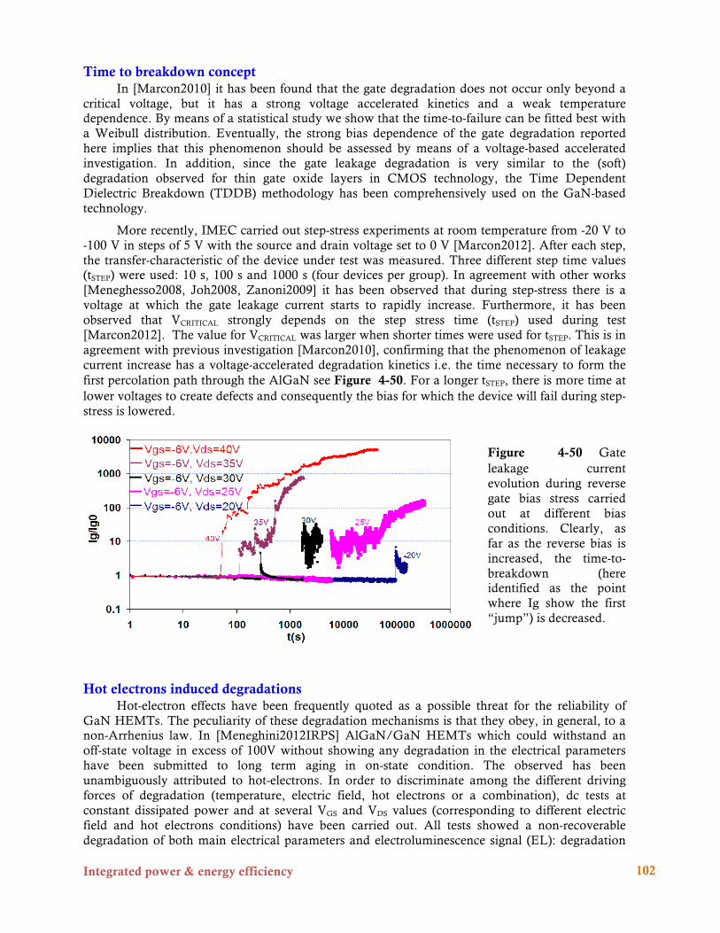
Integrated power & energy efficiency
102
Time to breakdown concept In [Marcon2010] it has been found that the gate degradation does not occur only beyond a
critical voltage, but it has a strong voltage accelerated kinetics and a weak temperature dependence. By means of a statistical study we show that the time-to-failure can be fitted best with a Weibull distribution. Eventually, the strong bias dependence of the gate degradation reported here implies that this phenomenon should be assessed by means of a voltage-based accelerated investigation. In addition, since the gate leakage degradation is very similar to the (soft) degradation observed for thin gate oxide layers in CMOS technology, the Time Dependent Dielectric Breakdown (TDDB) methodology has been comprehensively used on the GaN-based technology.
More recently, IMEC carried out step-stress experiments at room temperature from -20 V to -100 V in steps of 5 V with the source and drain voltage set to 0 V [Marcon2012]. After each step, the transfer-characteristic of the device under test was measured. Three different step time values (tSTEP) were used: 10 s, 100 s and 1000 s (four devices per group). In agreement with other works [Meneghesso2008, Joh2008, Zanoni2009] it has been observed that during step-stress there is a voltage at which the gate leakage current starts to rapidly increase. Furthermore, it has been observed that VCRITICAL strongly depends on the step stress time (tSTEP) used during test [Marcon2012]. The value for VCRITICAL was larger when shorter times were used for tSTEP. This is in agreement with previous investigation [Marcon2010], confirming that the phenomenon of leakage current increase has a voltage-accelerated degradation kinetics i.e. the time necessary to form the first percolation path through the AlGaN see Figure 4-50. For a longer tSTEP, there is more time at lower voltages to create defects and consequently the bias for which the device will fail during step-stress is lowered.
Figure 4-50 Gate leakage current evolution during reverse gate bias stress carried out at different bias conditions. Clearly, as far as the reverse bias is increased, the time-to-breakdown (here identified as the point where Ig show the first “jump”) is decreased.
Hot electrons induced degradations Hot-electron effects have been frequently quoted as a possible threat for the reliability of
GaN HEMTs. The peculiarity of these degradation mechanisms is that they obey, in general, to a non-Arrhenius law. In [Meneghini2012IRPS] AlGaN/GaN HEMTs which could withstand an off-state voltage in excess of 100V without showing any degradation in the electrical parameters have been submitted to long term aging in on-state condition. The observed has been unambiguously attributed to hot-electrons. In order to discriminate among the different driving forces of degradation (temperature, electric field, hot electrons or a combination), dc tests at constant dissipated power and at several VGS and VDS values (corresponding to different electric field and hot electrons conditions) have been carried out. All tests showed a non-recoverable degradation of both main electrical parameters and electroluminescence signal (EL): degradation

Integrated power & energy efficiency
103
rate was found to have a strong dependence on the EL signal emitted by the devices during stress, and a negligible dependence on temperature. Degradation was therefore ascribed to electron trapping induced by hot electrons in the gate-drain access region. Also in [Tapajina2012] hot electron degradation has been proposed in GaN HEMTs. Devices stressed in OFF-state at room temperature showed strongest degradation than those stressed at higher temperature. The degradation mechanism was attributed to trap generation in the maximum-electric-field region that was proposed to be related to hot-carriers.
Contact/Metallization/Passivation-Stability As well described in [Leach2010], in addition to degradation inherent to the semiconductor
crystal itself, metallurgical issues such as metal–semiconductor diffusion, phase changes in metal stacks, and electromigration within the metal are sources of potential permanent degradation. Electromigration of the gate electrode metal, impurity activation, and contact diffusion effects are reasonably well understood particularly in conjunction with, e.g., GaAs-based devices. However, GaN-based devices push the metallization technology to its limit causing some metallurgical changes, particularly under prolonged high-current or high-temperature operation. Ti/Al-based metallization schemes are typically utilized for the Ohmic contacts to AlGaN/GaN HFET structures and indeed are being used by the commercial entities. Reports on thermal stability are difficult to compare since various authors use different thermal stressing schemes to ascertain the quality of their ohmic contact metallization, but long-term thermal stability tests (representing aging of the device) have been demonstrated with some success in terms of minimal to no change in the contact resistivity of the ohmic metals in some systems. However, there is no universal consensus as to the best metal scheme to employ in terms of performance and long-term reliability, although the Ti/Al/Ni/Au is likely the most widely adopted. In terms of the thermal stability, the ohmic contacts are likely less of an issue as compared to the Schottky contacts [Sozza2005], which even in the absence of applied bias, may show some change with time under elevated temperatures. In case of Schottky, interdiffusion of the metals at elevated temperatures would obviously be an issue for the reliability. In fact, Pt-Au interdiffusion is known to occur at temperatures as low as 200°C. Although it is unclear precisely what role gate leakage plays in the degradation of the HFETs, it has been suggested that a silicide can form in devices employing Ni-based Schottky contacts and SiNx passivation layers at the SiNx–Ni interface and that the reduced barrier height of the Ni–silicide contact causes higher gate leakage. Additionally, the nonuniform nature of the silicide results in localized leakage conduction paths, which results in current crowding and gate electrode degradation, an increased instance of the “sudden degradation” phenomenon, and much lower device lifetimes [Ohki2009].
References [Adivarahan2003] V. Adivarahan et al., “Submicron gate Si3N4/AlGaN/GaN–metal–insulator–
semiconductor heterostructure field-effect transistors,” IEEE Electron Device Lett., vol. 24, no. 9, pp. 541–543, Sep. 2003.
[Bahat2008] Bahat-Treidel, E.; et al.,” Punchthrough-Voltage Enhancement of AlGaN/GaN HEMTs Using AlGaN Double-Heterojunction Confinement”, IEEE Transactions on Electron Devices, vol: 55 , no: 12, pp. 3354 – 3359, 2008
[Bahat2010] Bahat-Treidel, E.; et al., “AlGaN/GaN/AlGaN DH-HEMTs Breakdown Voltage Enhancement Using Multiple Grating Field Plates (MGFPs”), IEEE Transactions on Electron Devices, vol.: 57 , no: 6, pp. 1208 – 12162010, 2010
[Binari2001] S. C. Binari, et al., “Trapping effects and microwave power performance in AlGaN–GaN HEMTs,” IEEE Trans. Electron Devices, vol. 48, pp. 465–471, Mar. 2001.
[Chini2012] A. Chini, et al., “Experimental and Numerical Correlation between Current-Collapse and Fe-doping Profiles in GaN HEMTs” IRPS2012, International Reliability Physics Symposium, Anaheim, CA, USA, April 15-19, 2012.

Integrated power & energy efficiency
104
[Choi2006] Y. C. Choi, et al., “The effect of an Fe-doped GaN buffer on OFFstate breakdown characteristics in AlGaN/GaN HEMTs on Si substrate,” IEEE Trans. Electron Devices, vol. 53, no. 12, pp. 2926–2931, Dec. 2006.
[Chowdhury2008] Chowdhury, U. et al.: TEM observations of crack- and pit-shaped defects in electrically degraded GaN HEMTs. IEEE Electron Dev. Lett,, 29 (10) (2008), 1098–1100.
[Chu2008] R. Chu, et al., “Plasma treatment for leakage reduction in AlGaN/GaN and GaN Schottky contacts,” IEEE Electron Device Lett., vol. 29, no. 4, pp. 297–299, Apr. 2008.
[Chu2011] R. Chu, et al., “1200-V Normally Off GaN-on-Si Field-Effect Transistors With Low Dynamic ON-Resistance”, IEEE Electron Device Letters, Vol. 32, No. 5, pp. 632-634, 2011.
[Daumiller2001] I. Daumiller, et al., “Current instabilities in GaN-based devices,” IEEE Electron Device Lett., vol. 22, pp. 62–64, Feb. 2001.
[Douglas2012] E.A. Douglas, et al., “Investigation of the effect of temperature during off-state degradation of AlGaN/GaN High Electron Mobility Transistors”, Microelectronics Reliability 52 (2012) 23–28
[Green2000] B. M. Green, et al., “The effect of surface passivation on the microwave characteristics of undoped AlGaN–GaN HEMTs,” IEEE Electron Device Lett., vol. 21, pp. 268–270, June 2000.
[Hikita2005] M. Hikita, et al., “AlGaN/GaN power HFET on silicon substrate with source-via grounding (SVG) structure,” IEEE Trans. Electron Devices, vol. 52, no. 9, pp. 1963–1968, Sep. 2005.
[Ikeda2008] N. Ikeda, et al., “High power AlGaN/GaN HFET with a high breakdown voltage of over 1.8 kV on 4-inch Si substrate and the suppression of the current collapse,” 20th Int. Symp. Power Semicond. Devices ICs, Orlando, FL, May 18–22, 2008, pp. 287–290.
[Jimenez2002] A. Jimenez, et al., “Effect of p-doped overlayer thickness on RF-dispersion in GaN junction FETs,” IEEE Electron Device Lett., vol. 23, pp. 306–308, Apr. 2002.
[Jin2012] D. Jin and J. A. del Alamo, "Mechanisms responsible for dynamic ON-resistance in GaN high-voltage HEMTs", Proceedings of the 2012 24th International Symposium on Power Semiconductor Devices and ICs 3-7 June 2012 - Bruges, Belgium.
[Joh2007] Joh, J.; del Alamo, J.A.: Critical voltage for electrical degradation of GaN high-electron mobility transistors. IEEE Electron Dev. Lett., 29 (4) (2008), 287–289.
[Kohn2003] E. Kohn et al., “Transient characteristics of GaN-based heterostructure field-effect transistors,” IEEE Trans. Microwave Theory Tech., vol. 51, pp. 634–642, Feb. 2003.
[Koley2003] G. Koley, et al., “Slow transients observed in AlGaN HFETs: Effects of SiN passivation and UV illumination,” IEEE Trans. Electron Devices, vol. 50, pp. 886–893, May 2003.
[Leach2010] J. H. Leach, H. Morkoc, “Status of Reliability of GaN-Based Heterojunction Field Effect Transistors”, Proceedings of the IEEE, Vol. 98, No. 7, July 2010, pp.1127-1139
[Lee2012] H-S Lee, et al., “3000-V 4.3-mΩ · cm2 InAlN/GaN MOSHEMTs With AlGaN Back Barrier”, IEEE Electron Device Letters, Vol. 33, No. 7, July 2012, pp.982-984
[Lian2012] Y-W Lian, et al., “AlGaN/GaN HEMTs on Silicon With Hybrid Schottky–Ohmic Drain for High Breakdown Voltage and Low Leakage Current”, IEEE Electron Device Letters, Vol. 33, No. 7, July 2012 973
[Lu2010EDL] B. Lu, et al., “Schottky-Drain Technology for AlGaN/GaN High-Electron Mobility Transistors”, IEEE Electron Device Lett., vol. 31, no. 4, pp. 302– 304, April. 2010.
[Lin2010] Y-S Lin, et al., “AlGaN/GaN HEMTs With Low Leakage Current and High On/Off Current Ratio”, IEEE Electron Device Lett., vol. 31, no. 2, pp. 102–104, Feb. 2010.
[Lu2010DRC] B. Lu et al., “Breakdown Mechanism in AlGaN/GaN HEMTs on Si Substrate.” Proceedings of the Device Research Conference (DRC), 2010. 193–194.
[Marcon2010] D. Marcon, et al., “A Comprehensive Reliability Investigation of the Voltage-, Temperature- and Device Geometry-Dependence of the Gate Degradation on state-of-the-art GaN-on-Si HEMTs”; 2010 IEEE International Electron Devices Meeting, San Francisco, CA December 6-8, 2010.
[Marcon2012] D. Marcon, et al., “Reliability of AlGaN/GaN HEMTs: Permanent leakage current increase and output current drop”, Microelectronics Reliability, Vol. 52, no. 9–10, Pages 1751-2512, pp. 2188-2193, 2012
[Medjdoub2012] F. Medjdoub, et al., “First Demonstration of High-Power GaN-on-Silicon Transistors at 40 GHz”, IEEE Electron Device Letters, Vol. 33, No. 8, pp. 1168-1170, 2012
[Meneghesso1996] G. Meneghesso, et al., “Evidence of interface trap creation by hot electrons in AlGaAs/GaAs HEMTs,” Appl. Phys. Lett., vol. 69, no. 10, pp. 1411–1413, Sept. 1996.
[Meneghesso2008] G. Meneghesso , et al., “Reliability of GaN highelectron- mobility transistors: State of the art and perspectives,” IEEE Trans. Device Mater. Rel., vol. 8, no. 2, pp. 332–343, Jun. 2008.
Integrated power & energy efficiency
105
[Meneghini2012EDL] M. Meneghini, et al., “Time- and Field-Dependent Trapping in GaN-Based Enhancement-Mode Transistors With p-Gate”, IEEE Electron Device Lett., v.33, pp. 375-378, 2012
[Meneghini2012APL] M. Meneghini, et al., “Time-dependent degradation of AlGaN/GaN high electron mobility transistors under reverse bias”, Applied Physics Letters 100, 033505 (2012)
[Meneghini2012IRPS] M. Meneghini, et al., “Impact of Hot Electrons on the Reliability of AlGaN/GaN High Electron Mobility Transistors” IRPS2012, International Reliability Physics Symposium, 2012 Anaheim, CA, USA, April 15-19.
[Ohki2009] T. Ohki, et al., “Reliability of GaN HEMTs: Current status and future technology” in Proc. 47th. Int. Reliab. Phys. Symp., Montreal, QC, Canada, 2009, pp. 61–70.
[Park2009] Park, S.Y. et al.: Physical degradation of GaN HEMT devices under high drain bias reliability testing. Microelectron. Reliab., 49 (2009), 478–483.
[Piner2006] E. L. Piner, et al., “Device degradation phenomena in GaN HFET technology: Status, mechanisms, and opportunities,” in IEDM Tech. Dig., 2006, pp. 411–414
[Selvaraj2009] S. L. Selvaraj, et al., “Breakdown enhancement of AlGaN/GaN HEMTs on 4-in silicon by improving the GaN quality on thick buffer layers,” IEEE Electron Device Lett., vol. 30, no. 6, pp. 587– 589, Jun. 2009.
[Saito2005TED] W. Saito, M. Kuraguchi, et al.,, “Influence of surface defect charge at AlGaN–GaN-HEMT upon Schottky gate leakage current and breakdown voltage,” IEEE Trans. Electron Devices, vol. 52, no. 2, pp. 159–164, Feb. 2005.
[Saito2005TED2] Saito, W.; et al., “Design optimization of high breakdown voltage AlGaN-GaN power HEMT on an insulating substrate for RONA-VB tradeoff characteristics”, IEEE Transactions on Electron Devices, Vol. 52, no. 1, pp. 106 – 111, 2005.
[Saito2007] W. Saito, et al., “Suppression of dynamic on-resistance increase and gate charge measurements in high-voltage GaN-HEMTs with optimized field plate structure,” IEEE Trans. Electron Devices, vol. 54, no. 8, pp. 1825 – 1830, Aug. 2007
[Srivastava2011] Srivastava, et al., “Record Breakdown Voltage (2200 V) of GaN DHFETs on Si With 2- um Buffer Thickness by Local Substrate Removal”, IEEE Electron Device Lett., vol. 32, no. 1, pp. 30–32, 2011.
[Tapajina2012] M. ˇTapajna, et al., “Non-Arrhenius Degradation of AlGaN/GaN HEMTs Grown on Bulk GaN Substrates” IEEE Electron Device Letters, Vol. 33, No. 8, pp.1126-1128, 2012
[Tirado2007] J.M.Tirado, J.L. Sánchez-Rojas, J.I Izpura, "Trapping Effects in the Transient Response of AlGaN/GaN HEMT Devices" IEEE Trans. on Electron Devices, Vol. 54, No. 3, pp. 410-417, 2007
[Treu2009] Trew, R.J.; et al., AlGaN/GaN HFET reliability. IEEE Microw. Mag., 10 (4) (2009), 116–127. [Umeda2010] H. Umeda, et al., “Blocking-Voltage Boosting Technology for GaN Transistors by Widening
Depletion Layer in Si Substrates”, Tech. Digest 2010 IEEE Int. Electron Devices Meeting, San Francisco, CA December 6-8, 2010.
[Uren2006] M. J. Uren, et al., “Punchthrough in short-channel AlGaN/GaN HFETs,” IEEE Trans. Electron Devices, vol. 53, no. 2, pp. 395–398, Feb. 2006.
[Uren2012] M. J. Uren et al., “Buffer Design to Minimize Current Collapse in GaN/AlGaN HFETs” IEEE Transactions on Electron Devices, Vol. 59, No. 12, pp. 3327-3333, 2012
[Vetury2001] R. Vetury, et al., “The impact of surface states on the dc and RF characteristics of AlGaN–GaN HFETs,” IEEE Trans. Electron Devices, vol. 48, pp. 560–566, Mar. 2001.
[Visalli2010] D. Visalli et al. “Limitations of Field Plate Effect Due to the Silicon Substrate in AlGaN/GaN AlGaN DHFETs”, IEEE Transactions On Electron Devices, Vol. 57, No. 12, pp. 3333- 3339, 2010
[Ye2005] P. D. Ye, et al., “GaN metal–oxide–semiconductor high-electrontransistor with atomic layer deposited Al2O3 as gate dielectric,” Appl. Phys. Lett., vol. 86, no. 6, pp. 063501 1-3, Jan. 2005.
[Zanoni2007] Zanoni, E. et al.: A review of failure modes and mechanisms of GaN-based HEMTs, in Proc. of the IEEE Int. Electron Device Meeting (IEDM), 2007, 381–384.
[Zanoni2009] Zanoni, E. et al.: Localized damage in AlGaN/GaN HEMTs induced by reverse bias testing. IEEE Electron Dev. Lett., 30 (5) (2009), 427–429
[Zhou2012] C. Zhou, et al., “Vertical Leakage/Breakdown Mechanisms in AlGaN/GaN-on-Si Structures”, Proceedings of the 2012 24th International Symposium on Power Semiconductor Devices and ICs - Bruges, Belgium, 3-7 June 2012

Integrated power & energy efficiency
106
High temperature performances, thermal management, Limits of High temperature operation
Contributors: Oliver Ambacher (Fraunhofer IAF) Jean Jacques Aubert (CEA – Leti) Jean-‐Pierre Ganne (Thales Research & Technology) Eckart Hoene (Fraunhofer-‐IZM) Gaudenzio Meneghesso (University of Padova and IUNET) Peter Moens (ONSemiconductor) Joachim Pelka, (Fraunhofer VµE)
Abstract Increasing the working temperature of power devices and modules is a key issue for improving and simplifying the heat exchangers and cooling systems of power applications as well as for introducing power devices in high temperature environments such as deep drilling or aeronautics. New technologies around wide bandgap semiconductors, silicon carbide and gallium nitride mainly, are important breakthroughs to walk around the intrinsic temperature limitations of silicon technology. But if the new materials themselves are able to stand very high operation temperatures, the limitations may occur at the device level and also at the module level and the system level. At the device level, the diffusion processes can reduce the lifetime but the main issue will certainly appear at the metallization level, increasing electromigration and needing the shift from aluminum to copper. At the module level, increasing the working temperature require the removal of insulating gels and change in the packaging polymers nature. Thermal management will be the key. At the system level, increasing working frequency and temperature at the same time as well as the need for compactness will need to put the gate drives as close as possible to the devices asking for high temperature silicon logic technologies. And finally, one of the main temperature limitation can come from the passive components, essentially capacitors and their dielectric materials. A great attention has to be paid to this particular point.
Wide bandgap devices High performance power electronic circuits are expected to make a major impact on various applications spamming from power supply converters, automotive, aircrafts, satellites, and others. Si-based power devices cannot meet the temperature, voltage, switching speed, size and efficiency requirements to realize these benefits. Wide bandgap semiconductors, particularly SiC and GaN, are well suited to meet these requirements. The wide bandgap results in very low intrinsic carrier concentration that provides negligible junction leakage current up to 500°C [mishra2002]. This allows high temperature operation cooling requirements. The high breakdown strength of SiC and GaN results in thinner drift layers for a given blocking voltage, as compared to silicon, thus reducing the specific on resistance and storage of minority carriers. Recently, there has been a renewed interest in high-resistivity Si substrates owing to their low cost, availability in large size, and good thermal conductivity (of 1.57 W/cm · K) that helps minimize self-heating effects in the overlying epilayers.

Integrated power & energy efficiency
107
Temperature characteristics of GaN HEMT and MOSFET devices In [Vitanov2010] a very detailed modeling of the material thermal has been carried out in GaN on SiC substrate; they performed two-dimensional hydrodynamic electro-thermal simulations with our device simulator Minimos-NT, which proved to be a suitable tool for the analysis of heterostructure devices. Their setup allows for a proper modeling of the drain current also at elevated temperatures. As an example, Figure 4-51 shows the output characteristics at 425 K. Two curves are shown for VGS = 2 V: without self-heating, which greatly overestimates the current; with self-heating, which delivers a significantly better match, but requires a higher computational effort. Clearly in [Vitanov2010] current density decrease at increasing temperature, in agreement with other studies [Pérez-Tomás2009], see Figure 4-52, carried out either in Schottky and MOS gate structures.
Figure 4-51 Calibrated output characteristics versus experimental data for Lg = 0.25 um HEMT at 425 K. Dot-dashed line-w/o self-heating, solid line-with self-heating.
Figure 4-52 (a) Transistor on resistance Ron at VDS=0.5 V vs temperature for MOSFETs (with different definitions of the active area) and HEMTs and (b) contact resistivity evolution with temperature
A detailed study on the high-temperature performance of AlGaN/GaN MOSHEMT with SiO2 gate insulator fabricated on Si (111) substrate has also been recently reported [Husna2012] and compared with those of references AlGaN/ GaN HEMTs. The device dc parameters, such as the drain-source current (IDS), extrinsic transconductance (gme), subthreshold currents, and gate–source leakage currents (IGS) were measured and evaluated. Both types of transistors were found to exhibit a maximum output current density of about 0.73 A/mm at room temperature (RT) and very low specific ON-resistances between 0.42 and 0.52 mΩ·cm2. Figure 4-53 shows typical dc I–V characteristics of the AlGaN/GaN MOSHEMT and conventional HEMT on Si (111) measured for devices with a gate length LG = 2.5 um, a gate width WG = 1 × 100 µm, and a drain–gate opening of 4µm. The data were measured at RT and 200 °C, and the gate voltage was swept from VGS = +2 V to −6 V in −1 V steps. The saturation output current show a relatively smaller degradation in both devices.

Integrated power & energy efficiency
108
Figure 4-53 Typical dc output characteristics of AlGaN/GaN (a) HEMT and (b) MOSHEMT on Si (111) substrate measured at RT and 200 C. The two types of devices were processed on the same wafer using exactly the same procedure, except for the additional step of SiO2 deposition under the MOSHEMT’s gate.
Figure 4-54 Subthreshold drain–source leakage current in AlGaN/GaN HEMT and MOSHEMT on Si. Figure 4-54 shows typical subthreshold characteristics of HEMTs and MOSHEMTs at RT and 200 °C. At 200 °C, the subthreshold drain-source leakage currents were 300 µA/mm for the HEMT and about 30 times smaller for the MOSHEMT (at ∼10 µA/mm) even though the degradation rate of the residual current at elevated temperatures was much faster for the latter device. On the other hand, the subthreshold slope was 410–500 mV/decade for the MOSHEMTs as compared to ∼300 mV/decade for HEMTs. The corresponding RT subthreshold slope values were 100 and 120 mV/decade, respectively. The larger increase in the subthreshold slope for the MOSHEMTs under thermal stress probably originates from the activation of interface states introduced by the SiO2 dielectric. The outcome of these characterizations establishes the SiO2/AlGaN/GaN MOSHEMTs on Si as a promising alternative for cost-effective and high-

Integrated power & energy efficiency
109
temperature power electronic systems owing to an improved performance as compared to their Schottky counterparts. However, this statement must be taken with great attention, since other studied has highlighted the important negative effect of scattering effects at the insulator/semiconductor interface that induce large mobility degradation [Pérez-Tomás2009].
Temperature characteristics of SiC-based devices The most suitable and established SiC polytype for high temperature power electronics is the hexagonal 4H polytype. The main advantages related to material properties are: its wide bandgap, high electric field strength and high thermal conductivity. Almost all different types of electronic devices have been successfully fabricated and characterized. The most promising devices for high temperature applications are pn-diodes, junction field effect transistors and thyristors. MOSFET is another important candidate, but is still under development due to some hidden problems causing low channel mobility. The maximum operating temperature of a Schottky diode in SiC may be limited by an increasing leakage currents, but active power devices for operation at high temperature has been presented. UMOSFET (U-shaped trench Metal Oxide Semiconductor Field Effect Transistor) made from SiC that operate up to 450 C and thyristors (6 A, 700 V) that operate at 350 °C have been presented. Furthermore, SiC MOSFETs have been reported to operated even at 650 °C.
High temperature packaging The limitations of actual packaging technologies coming to higher temperatures are to a significant part life time limits. Packages are designed to reach a defined life time before thermo-mechanical wear out. Up to now these limits are mostly lower than the maximum allowed temperature of the package and therefore increasing this temperature has to come along with improved thermo-mechanical reliability. The reason for the thermo-mechanical wear out is the mismatch of the thermal expansion of the materials used in the package. Thereby materials and interfaces are mechanically stressed when warming up and cooling down again and fail after a certain time of operation. Therefore two aspects have to be solved coming to higher temperatures: the temperature stability of all used materials and a reduction of thermo-mechanical mismatch. The packaging challenges to be solved are:
• Semiconductor metallization Diffusion barriers between semiconductor and metallization have to be enhanced for higher temperature operation. Surface metallization like Aluminum will come to its limits and will not be suited any more
• Electrical conductors The biggest share of power semiconductors are vertical devices. They are mostly attached to a conductor providing the electrical connection and that is part of the major heat path. As the well conducting metals have a high coefficient of thermal expansion (CTE) this leads to thermo-mechanical stress between conductor and the low CTE chip. In power modules this problem is solved by using DCB (Direct Copper Bond) or comparable substrates. Here the ceramic substrate forces the metal to a lower CTE by a high stability interconnect. At higher temperatures this does not work properly any more, as the mechanical stability of the ceramic is reached. Therefore there is a need for a thermally and electrically well conducting material with low CTE at a reasonable price.
• Encapsulation Encapsulation materials are mostly based on silicone or epoxy basis, where especially the epoxy is limited in temperature. Here material development is required (see Chapter Packaging).
• Thermally conducting Insulator
Integrated power & energy efficiency
110
Ceramic substrates are in principle suited for higher temperatures. Future challenge will be to develop a substrate with metallization, that can withstand higher thermal cycles compared to the current power substrates.
• Package innovations Thermo-mechanical stress can be reduced by innovations in the package structure. If interfaces can be decoupled mechanically cracks or delaminations are avoided. On the other hand mechanical decoupled interfaces still have to conduct thermally and electrically. Here basic research is necessary, which materials are suited to act as thermal interface material for low roughness surfaces (e.g. semiconductor chips), how their performance and long term stability is and how these packages can look like.
High temperature Gate drives The application temperature of microelectronic circuits has been steadily increasing over the
years. This is due to new challenges regarding energy efficiency, reduction of emissions, and reduction of system size, for example in the automotive and aviation markets. While some years ago 125°C was considered the maximum required temperature in automotive application today customers ask for 150°C and even 175°C. Better motor control to reduce emission and the introduction of electronic actors demand for even higher temperatures in the near future. The exploration of natural energy resources (gas, oil, geothermal) is a high tech operation with sophisticated sensor and data acquisition systems that are among the core technologies to enable deep hole drilling. Today´s deep hole drilling requires system function at temperatures close to 200°C, the next generation of explorations fields will require temperatures in excess of 200°C. The demand for energy efficiency pushes the microelectronic technology industry to develop high performance power electronics systems. Whether for niche markets or global applications, power electronic devices must deliver high performance in term of compactness, reliability and efficiency. The recent availability of power devices based on GaN and SiC offer the potential for making significant progress since they can operate at temperatures beyond 200°C, increasing overall system efficiency and drastically reducing cooling effort and package size. However, in order to exploit the high temperature capability of these new power devices the CMOS control electronics must also be able to operate at these high temperatures. Due to exponentially increasing leakage currents with higher temperature standard circuits based on CMOS technology that are available today have an upper limit of typically 150°C, in special cases of 175°C.
Thus, there is a need to develop a high temperature CMOS technology with 0.35µm structure size for application temperatures of up to 250°C. The technology is based on Silicon On Insulator (SOI) wafers which suppresses the detrimental leakage currents to a large extent. Currently worldwide only two companies offer high temperature electronics based on SOI for temperatures over 200°C, however with structure size 0.8µm and larger, no non-volatile memories and limited access/reliability.
Driving the new wide band gap SiC and GaN devices will therefore need a large step beyond the state of the art towards complex highly integrated electronic circuits for high temperature applications.
Passives for High Temperature Power Electronics
Challenges for passive components: capacitors and inductors or transformers Nearly all the passive components used to-day in electronics were developed for a working temperature range from –50°C to 125°C. Recently the needs of high temperature operation for the new applications with growing importance such as oil drilling, automotive etc… led the producers to extend their component offer towards higher working temperatures, but in most cases they are still limited to 200°C or 250°C in the best cases, and hardly no solution for passive components working at higher temperatures such as 300 or 400°C.

Integrated power & energy efficiency
111
The emergence of new semiconductor technologies such as SOI, SiC, GaN will be a suitable answer to the needs of high temperature operation, on the condition that that the packaging technologies and the passive components evolve in the same direction. To-day three main technologies are used for storage and filtering capacitors, every one with its own applicability domain:
- electrolytic capacitors (with liquid or solid electrolyte) - polymer film capacitors - multilayer ceramic capacitors.
The electrolytic capacitors using liquid electrolytes are severely limited towards high temperature by the boiling point of their electrolyte. Aqueous electrolytic capacitors cannot be used above 80°C. For reaching higher operation temperature it is necessary to develop new liquid (organic) electrolytes with higher boiling points, or new composite gel electrolytes with a solid porous polymer network inside which the liquid phase can circulate freely and reach the electrode surfaces. These approaches could extend the use of these capacitors well above 80 °C and they are certainly ways to explore, also because they present close connections with the researches on high temperature batteries.
Tantalum capacitors are electrolytic capacitors with solid electrolyte. They are more naturally suited for high temperature operation because they are made mainly of metals (Tantalum, Silver), oxides (Tantalate, Manganite) and some organic composite of graphite or conducting polymer. To-day most tantalum capacitors are specified for operation up to 150°C. Indeed some companies are starting to offer tantalum capacitors working up to 200°C or more. According to them, the main problems to extend their use towards higher temperature ranges do not originate from the metal electrodes or from the layers of oxide, but from the organic materials used in this technology. Therefore one key to increase their working temperature is to find polymeric materials, either insulating or conducting, that withstand higher temperatures.
Polymer film capacitors are made from polymer dielectric films which are metallised and wound or stacked. They present a number of advantages. Thanks to the ability of polymers to withstand large breakdown fields, and to be shaped as rolls of relatively thin films, they present a relatively high volumetric capacity to store electric charge and energy. They can be produced easily in large quantities, with various shapes and sizes, at moderate cost. Unfortunately they present a poor ability to withstand high temperature, limited by their dielectric material. As of today, the most used materials are limited to 120°C. Some polymers can withstand much higher temperatures (up to 270°C) but they are difficult to produce in films and expensive. There is a strong need to find low-cost high-temperature metallised dielectric film materials that can be processed easily to make wound or stacked capacitors like present polymer film capacitors. Several promising ways are being explored in the literature, mainly in the USA, but it does not seem that any of these is more advanced: dielectric oxide thin films (e.g. PLZT, Hafnium oxide, silicon dioxide) on metal tape (Nickel, stainless steel, copper), new polymer or copolymer blends to make films etc… There seem to be very little (not to say no) research effort in Europe on this topic, this situation should be changed by encouraging research and development.
Multilayer ceramic capacitors have long been used for filtering in analog circuits or for decoupling the supply lines of integrated circuits in digital circuits. To-day they are the most numerous capacitor parts produced in the world (the order of magnitude is one trillion or 1012), and any consumer electronic apparatus contains tens or hundreds of those ones. The are particularly well suited for high temperature use because they are made only of inorganic materials (metals and ceramic oxides), and they are fabricated by co-firing together these materials at a very high temperature, typically higher than 1000°C. However they use ferroelectric oxides based on barium titanate, that present a very high dielectric constant (or relative permittivity) in the usual range of temperatures, but not at high temperatures, because barium titanate gets paraelectric above its

Integrated power & energy efficiency
112
Curie Temperature TC (120°C), and then its permittivity decrease according to Curie’s law as 1/(T-TC). Another problem is that Barium Titanate may contain charged defects whose migration is thermally activated. These defects give a negligible contribution to conduction and dielectric losses in the usual range of temperature, but this is no more the case at high temperatures. For these working conditions, new ceramic ferroelectric or relaxor dielectric need to be developed, with higher Curie temperatures, avoiding the use of Lead in their composition. Indeed PLZT could be good dielectric materials to substitute barium titanate because depending on their composition they can present higher Curie temperatures but unfortunately they contain lead. New complex dielectric compositions without lead and based for example on relaxor phase diagrams such as Bismuth-Zinc-Niobium Oxides, or “incipient” ferroelectric such as Silver-Niobium-Tantalum Oxides etc… should be evaluated for making multilayer ceramic capacitors for high working temperatures.
Concerning magnetic components such as transformers and inductors, to-day they are made of three parts:
- a yoke made of a soft magnetic material that can be metallic (such as permalloy, nanocrystalline finemet), composite (iron powder in polymer, thin metallic tapes encapsulated with polymer films) or ceramic (different types of ferrites)
- one or several conducting windings made of metallic wires or planar that must be isolated with a resin
- a mechanical holder or a casing in order to hold and protect the component Concerning the magnetic materials, their ability to keep their magnetic properties is driven by their Curie temperature above which they lose their ferromagnetic (or ferrimagnetic properties). Most magnetic metallic alloys present high Curie Temperature. For nanocrystalline or amorphous metallic alloys the problem is more the stability of the amorphous or nanocrystalline structure. For ferrites their Curie temperatures are lower, and present a strong dependence with composition, so that the choice of compositions is more limited for high temperature operation than for usual conditions. However the main obstacle to increase working temperatures is the use of organic materials for isolation, either in standard winding technology (where resins are used to isolate the conductors and to encapsulate the finished component) or in planar technology (where printed circuit boards are used to realize the windings). A possible solution is to use planar technology with printed circuit board for high temperature (see the part on PCBs for high temperature). Another more radical solution is to get rid of all organic materials by using a ceramic multilayer technology to realize the transformers and inductors with integrated windings. As a conclusion, the ultimate goal could be to integrate in the same LTCC substrate all the necessary passive components, lines, capacitors, inductors, transformers, by selecting materials that can be co-fired and present the required characteristics (permittivity, permeability, low losses) at the intended working temperature. References [mishra2002] U. K. Mishra, P. Parikh, and Y.-F. Wu, “AlGaN/GaN HEMTs—An overview of device
operation and applications,” Proc. IEEE, vol. 90, no. 6, pp. 1022–1031, Jun. 2002. [Tan2006] W. S. Tan, M. J. Uren, P. W. Fry, P. A. Houston, R. S. Balmer, and T. Martin, “High
temperature performance of AlGaN/GaN HEMTs on Si substrates,” Solid State Electron., vol. 50, no. 3, pp. 511–513, Feb. 2006.
[Husna2012] F. Husna, M. Lachab, M. Sultana, V. Adivarahan, Q. Fareed, A. Khan, “High-Temperature Performance of AlGaN/GaN MOSHEMT With SiO2 Gate Insulator Fabricated on Si (111) Substrate”, IEEE Transactions On Electron Devices, Vol. 59, No. 9, September 2012, p.2424
[Vitanov2010] S. Vitanov, V. Palankovski, S. Maroldt, R. Quay, “High-temperature modeling of AlGaN/GaN HEMTs”, Solid-State Electronics 54 (2010) 1105–1112
[Pérez-Tomás2009] A. Peres-Tomás, M. Placidi, N. Baron, S. Chenot, Y. Cordier, J. C. Moreno, A. Constant, P. Godignon, and J. Millán, “GaN transistor characteristics at elevated temperatures,” J. Appl. Phys., vol. 106, no. 7, p. 074519, Oct. 2009

Integrated power & energy efficiency
113
Packaging issues and solutions for Power devices
Eckart Hoene (Fraunhofer-‐IZM) With the contribution of:
Jean Jacques Aubert (CEA – Leti) Klaus Heyers (Bosch) Angelo Magrì (STMicroelectronics) Joachim Pelka, (Fraunhofer VµE) Lothar Schindele (Bosch)
Abstract
The evolution of power semiconductors has arrived at a level where packaging restricts the achievable performance of the final device. A package for a power semiconductor has to remove the heat, provide security insulation against the heat sink, conduct current and has to be electromagnetically and thermo mechanically reliable. The development of solutions for these multiple requirements has to be based on in depth knowledge of application demands as well as material and production. This complexity is one reason, why European companies still have a leading position in the world market.
The future development of packages has to face the following aspects:
• The increase of power density requires more sophisticated thermal design • The possibility for higher junction temperatures can only partly be used due to the reduced
live time of the package. A higher temperature would reduce system volume due to smaller heat sinks. This is especially valid for semiconductors with wide band gap like SiC an GaN.
• More functions included in the power semiconductor package can reduce system costs • Higher switching slopes force a more precise electro-magnetic design of the package and
will influence the technology selection. • Packaging technologies with longer life time pay off by reduced system costs • Production processes always remain an issue for improvements
In this chapter these aspects will be worked out in detail with examples for applications.
New packaging technologies for high power modules Decentralized energy generation by renewable sources significantly increases the amount of
power electronics needed in the higher power range. To control energy generation, flow and consumption efficiently, power electronics with higher voltages and high currents are necessary to be able to handle high energies. At the same time the reliability for high power applications is crucial. To face these requirements the research and development for Semiconductor Packages has to tackle the following questions:
1. Improvement of reliability Improved reliability reduces system costs due to lower efforts for cooling and/or costs of ownership due to reduced maintenance. It can be achieved by optimization of interconnects, the Die attach, new materials and encapsulation (see below). As power modules will always be designed for a limited life time, state of health monitoring is a solution to avoid stand still due to an unexpected maintenance. Research has to be carried out to make this kind of monitoring possible and cost efficient.

Integrated power & energy efficiency
114
2. Balancing series and parallel connected chips Faster switching speeds can help to reduce system costs in many applications. At higher power levels the current and voltage handling capability of single semiconductor chips is mostly not sufficient and parallel and/or series connections have to be used. These connections can be handled at nowadays switching speed, but in future handling the static and dynamic unbalance will require more effort in design and degrees of design freedom by the package. Therefore suited technologies have to be developed, that allow lower inductance setups, knowledge on designing parasitic effects and integration of switching cells in the package.
3. Packages for high voltage applications with series connected semiconductors The insulation of the semiconductors to the heat sink is restricted to approx. 10 kV using ceramic substrates. At higher voltages mostly air is used as insulator, this decreases the power density tremendously. In these cases the heat sinks are not on ground potential anymore and need to be cooled by non conducting fluids like oil. Future research has to focus these challenges by reducing semiconductor losses, improved insulation strategies and innovative cooling solutions. The package development has to interact with inverter development to come to generate maximum benefit.
High efficient double sided cooling technology (for E-Mobility) In hybrid cars the coolant temperature is high compared to other applications. Therefore
double sided cooling of semiconductors pays of, as less chip area is needed for the same power handling capability. There are several issues to be solved for this kind of package:
1. Reduction of thermal impedance on both sides of the chip To achieve a benefit from double side cooling the thermal path on both sides has to be low. Therefore a low number of layers between the chip and the coolant is required that have to show high thermal conductivity. The required safety insulation to both sides up to now is solved by two DCB substrates. As they severely bend in opposite direction during manufacturing mechanical stress is brought into interconnects. This results in a low lifetime and has to be solved.
2. Insulation Mounting chips upside down requires new solutions for insulation, as the distances between different potentials are much lower than in conventional packages. Furthermore the classical insulation materials are not suited, e.g the silicone due to its high CTE and the missing possibility to expand and the Transfer Mold Technology due to its limited ability to fill long and thin gaps. Here new solutions have to be developed.
At the same time the double sided cooling technology has to pay off by reducing the required amount of silicon chips, therefore the extra effort on packaging has to come down to a level lower than the saved silicon costs.
Embedding Embedding semiconductors into a PCB like substrate has recently shown to be an alternative
to the classical packaging process with die attach, wire bonds and encapsulation. Up to now low cost packages are manufactured by this technology, the cost reduction is mainly achieved by the batch type production process. Nevertheless there are more opportunities to be taken. The technology offers an easy integration of other functions into a package, as the border between PCB and components dissolves. A PCB can be used to package a single semiconductor as well as a semiconductor can be integrated into a PCB which will be assembled in a standard SMD process. Furthermore the height of semiconductor packages can be reduced, as vertical interconnections are replaced. Finally the increased number of layers allows a more flexible design, which is required for very fast switching semiconductors.

Integrated power & energy efficiency
115
Open aspects which require research in this area are: § Materials with higher temperature resistance able to work at junction T of 175°C. § Insulation materials for safety insulation and high thermal conductivity § Qualification of material and production process for power needs: Insulation, Power
cycling, life time
Die attach The Die attach has been dominated by soldering for decades. Recently several alternatives
were developed and are in different stages of market acceptance: the low temperature silver sintering, the transient liquid phase bonding (TLPB) and the transient liquid phase soldering (TLPS). Silver sintering offers superior reliability properties compared to soldering, major drawback is the manufacturing process. Up to now pressure and temperature are needed to form the joint and this increases production time significantly. Although this interconnect seems to be the solution for high temperature interconnects, a significant lifetime decrease of the joint was observed at temperatures of 175°C and 200°C [Mer04]. TLPB also promises high reliability, but is not yet fully qualified and commercialized. Compared to silver sintering it has advantages due to the lower required pressure and faster manufacturing. Nevertheless TLPB requires joining surfaces with lower roughness as its layers have to be thin. TLPS could be an alternative. Research effort is required for the following aspects:
§ Development of pastes for pressure less silver sintering § Development of sintering pastes for direct application to copper § High temperature stability of sinter joints § Process development and qualification of TLPB/TLPS
Top side interconnects Although many alternatives to standard aluminum bond wires were developed recently, the
majority of semiconductors are packaged in this classical way. The alternatives can be clustered in different categories:
§ Metallurgical modifications of aluminum § Combinations of different metals § Copper wires with copper surfaces on the chips § Galvanic copper (see chapter “Embedding”) § Sintered top side contacts
Furthermore geometrical modifications for wires and tools are tested. All of these technologies have promising properties either in reliability, current capability, inductance or manufacturing. Nevertheless research has to be carried out in process development, qualification and materials. Especially the copper metallization of chips is not qualified for mass production yet.
Encapsulation Materials used mostly for encapsulation in power electronics are Silicone and Epoxy Mold
Compound (EMC). Silicone is well suited to be used also in higher temperature applications while EMC requires modifications in future. Coming to higher semiconductor temperatures resins with high glass temperature and high amount of fillers are required towards packages with 250°C junction temperature. As there are resins with glass temperature above 280°C there is a chance to reach this goal with intensified research effort. Another research path is the integration of power and control circuitry in a package. There mainly the reduction of warpage of these packages with very different materials and components inside is a critical topic as well as the increase of operation temperature by reduction of thermal mismatch.
References [Mer04] Mertens, C., „Die Niedertemperatur-Verbindungstechnik der Leistungselektronik“, Dissertation, TU Braunschweig, 2004

Integrated power & energy efficiency
116
High power Passives for Inverter / Converter
Jean-‐Pierre Ganne (Thales Research & Technology France) With the contribution of:
Braham Ferreira (TUDELFT) Richard Lebourgeois (Thales Research & Technology France) Jelena Popovic (TUDELFT)
Abstract Magnetic components ( inductors and transformers) are the limiting factor for the miniaturization of Switched-Mode Power Supplies. Increasing their switching frequencies enables to miniaturize magnetic components, but materials properties and component designs vary with frequency. Wide-Band semi-conductors components opens the way to Multi MHz switching , but the materials and designs used for passive components in present high frequency (several 100 kHz) SMPS cannot be transposed. New materials and new designs must be developed for Multi MHz passive components. The following chapter is divided into three parts. In the first part we explain why high-frequency switching enables to miniaturize the passives, and how the choice of magnetic materials is closely linked with the switching frequency. We introduce a merit factor for power magnetic materials that characterizes their ability to transmit a high volumetric density of power with low power dissipation. We show how the preferred choice of magnetic materials, based on this criteria, depends on switching frequencies. In the second part we identify three current trends in the evolution of magnetic components: the development of new materials, the replacement of bulky components with planar shapes, and the research of technologies able to integrate the conductors with the magnetic materials inside a monolithic ceramic component, made by a multilayer ceramic technology. Although multilayer ceramic capacitors, chip inductors, and multilayer ceramic substrates have long been fabricated in this way, integrating different ceramic materials with metallic conductors in order to make multilayer integrated passive components is still a big challenge. To date only partial integration has been demonstrated, for instance of high-k materials for capacitors inside low-k ceramic substrates. In the third and last part four challenges are identified for the future research: High frequency, high power magnetic materials, Low thermal resistance and low dissipation, Components and windings at very high frequency, Capacitors and integrated passive components.
Magnetic components and frequency evolution of SMPS (from kHz to multi MHz)
Magnetic and dielectric oxides (ferrites and perovskites) are used in passive components such as inductors, transformers and capacitors.
In switched-mode power supplies, the choice of the soft magnetic materials used for manufacturing transformers and inductors depends on their switching frequency. The power density transmitted by a transformer is proportional to the product B×f of the induction B with the frequency f. Therefore, the B×f product is used as a figure of merit to compare different magnetic

Integrated power & energy efficiency
117
materials, and there is a trend to increase switching frequencies of power supplies in order to decrease the size and weight of magnetic components.
Increase of switching frequency allows the size reduction of reactive passive components : capacitors and magnetic components which are the biggest, because in a circuit Cω or Lω are given, and C or L is size dependent. If ω increases, the necessary values C or L decrease, and the sizes of components decrease.
New WBG power active components enable working at high switching frequencies above 1 MHz with high efficiency. Today the switching frequency of high power density converters is limited to about 100 – 500 kHz, above these frequencies switching losses become too high, but new GaN active components will enable working at higher frequencies (1-5 MHz).
The choice of magnetic materials depends on working frequencies. The following table gives a synthesis of current choices.
At low frequencies, one can use metallic materials because they present the highest saturation magnetization Bs, and the magnetic losses inside the materials remain low as long as B remains lower enough than Bs (typically B < 0,5 Bs), and the losses by eddy currents are moderate. Typically one uses Soft Fe-Si or metallic alloys such as permalloys Fe-Ni-Co. Because the magnetic components are bulky and account for a large part of the volume and weight of the power converter, one tends to increase their working frequency in order to decrease their size, but eddy currents rapidly increase, which implies increased losses in metallic conducting materials. There are two ways to limit eddy currents, either by using less conducting materials or by structuring the materials with inner insulating barriers. In the first case one uses ferrites, in the second case composite materials such as magnetic powders in polymers or magnetic films (thick or thin) alternating with insulating layers. This last approach can be used at mean frequencies (1-10 kHz) with amorphous or nanocrystalline metallic materials but at higher frequencies the use of insulating materials (ferrites) is mandatory because the losses by eddy currents increase very fast with frequency and become prohibitive.
The best soft ferrites between 10 kHz and 1 MHz are Mn-Zn ferrites. Today these ferrites are frequency limited (f < 3 MHz) because their electrical resistivity is not high enough to prevent eddy current loss. Because of their high electrical resistivity (more than 1000 times higher than Mn-Zn
Material Permeability Frequency range
Metallic sheets or ribbons
(Conductive)
iron-silicon High> 1000
Low< 1 kHz
iron-nickel, iron-cobalt High> 1000
Low< 1 kHz
Amorphous, nanocrystallinemetallic alloys (FeSiB based)
Very High> 10 000
Medium< 100 kHz
Ferrites(Insulator)
Manganese-zinc ferrites High > 1000Very High, > 10 000
Medium10 to 1000 kHz
Nickel-zinc-(copper) ferrites Medium< 1000
High1 to 100 MHz
Metallic powder based Composites
(Insulator)
Iron, carbonyl ironLow, < 100Very low,
< 10
Medium10 to 1000 kHzIron-nickel-(molybdenum)
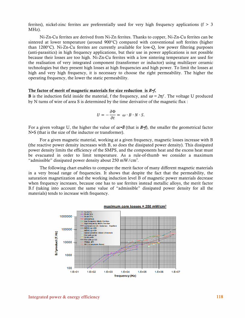
Integrated power & energy efficiency
118
ferrites), nickel-zinc ferrites are preferentially used for very high frequency applications (f > 3 MHz).
Ni-Zn-Cu ferrites are derived from Ni-Zn ferrites. Thanks to copper, Ni-Zn-Cu ferrites can be sintered at lower temperature (around 900°C) compared with conventional soft ferrites (higher than 1200°C). Ni-Zn-Cu ferrites are currently available for low-Q, low power filtering purposes (anti-parasitics) in high frequency applications, but their use in power applications is not possible because their losses are too high. Ni-Zn-Cu ferrites with a low sintering temperature are used for the realisation of very integrated component (transformer or inductor) using multilayer ceramic technologies but they present high losses at high frequencies and high power. To limit the losses at high and very high frequency, it is necessary to choose the right permeability. The higher the operating frequency, the lower the static permeability.
The factor of merit of magnetic materials for size reduction is Bf. B is the induction field inside the material, f the frequency, and ω = 2πf . The voltage U produced by N turns of wire of area S is determined by the time derivative of the magnetic flux :
𝑈 = −𝜕Φ𝜕𝑡
= 𝜔 ∙ 𝐵 ∙ 𝑁 ∙ 𝑆. For a given voltage U, the higher the value of ωB (that is Bf), the smaller the geometrical factor NS (that is the size of the inductor or transformer).
For a given magnetic material, working at a given frequency, magnetic losses increase with B (the reactive power density increases with B, so does the dissipated power density). This dissipated power density limits the efficiency of the SMPS, and the components heat and the excess heat must be evacuated in order to limit temperature. As a rule-of-thumb we consider a maximum “admissible” dissipated power density about 250 mW/cm3.
The following chart enables to compare the merit factor of many different magnetic materials in a very broad range of frequencies. It shows that despite the fact that the permeability, the saturation magnetization and the working induction level B of magnetic power materials decrease when frequency increases, because one has to use ferrites instead metallic alloys, the merit factor B.f (taking into account the same value of “admissible” dissipated power density for all the materials) tends to increase with frequency.

Integrated power & energy efficiency
119
Trends in the evolution of magnetic components Development of new ferrite materials To-day new commercial ferrites proposed are based on Mn-Zn ferrites but this not the best choice for frequencies well above 1 MHz, because their losses tend to increase faster at high frequencies than the losses of Ni-Zn ferrites. Indeed losses in Mn-Zn ferrites are dominated by eddy currents and domain wall relaxations and increase as f2, while in Ni-Zn ferrites losses are due to resonance-relaxation of spin rotation and are proportional to f. Today new Ni-Zn-Cu ferrites present lower losses than Mn-Zn ferrites at high power and high frequencies. The question is how to improve the power density (or decrease power losses) further?
Planar circuits based on Power PCB Conventional windings based on Copper wires or Litz Wire tends to be replaced with copper circuits in PCB. This presents many advantages: the components are flatter, the windings are easier to realize, the component are mounted easily, the flat shape favours the evacuation of heat. But there are also some drawbacks such as increased parasitic elements. There are strong interactions between windings, which must be taken into account in the design. The question is how to design windings and circuits at high frequencies?
Improved integration Increased integration of magnetic materials with windings Today magnetic materials, windings and connectors are produced separately and assembled. Conventional inductors and transformers are made by winding bulk ferrite parts, and soldering with leadframe and encapsulating them in polymer. Some companies propose different innovative processes. Example: Microspire Process. Multilayer ceramic technology enable to produce SMD (surface mounted) miniature inductors. But these components are low-Q and present losses, they are not optimized for power, LTCC technology is proposed for designing and producing inductors and transformers (examples: Via-Electronics, Nascent). LTCC technology could be used in order to integrate different passive functions (capacitive, resistive, inductive) in a single multi-layer ceramic substrate… Already partial integration of was demonstrated. For example: Embedded capacitors in a LTCC substrate (PIDEA Project Pacific Boat collaboration with Thales Microelectronics and Via-Electronics), see Figure 4-55.
Figure 4-55 Left: high-k material (brown, BZN made by Thales Research and Technology, K=80) co-fired with low-k material (Blue, DuPont 951, K=7). Right: the LTCC substrate was mounted
and tested on a PCB by BGA
-

Integrated power & energy efficiency
120
But we need to develop a set of different functional materials (dielectric, magnetic, resistive…) that can be assembled as tapes or screen-printed thick films, and co-fired (without interdiffusion, without warpage etc…). Other possibilities include various 3D prototyping techniques (ink-jet printing laser sintering etc…) allowing to assemble different materials (metal, low-k and high-k dielectrics, low-permeability and high-permeability magnetics).
Research directions on high frequency passive components: four challenges.
WB devices makes it possible to increase the power conversion frequencies at a given power level beyond what has been possible with Si devices. This takes the design of passive components into an unchartered fields. Experience obtained with RF circuits and power supplies for induction heaters could be useful but does not meet the specific requirements for many power electronic applications. Leading work in this field (for example, Perrault at MIT, Sullivan at Dartmounth and papers presented at the PowerSOC) have been dealing with magnetic components at multi MHz frequencies, but at low power and low voltage. Therefore fundamental and original research is necessary to design and construct suitable passive components; inductors, transformers as well as capacitors.
At elevated frequencies the design of the passive components becomes a tight compromise between managing the losses and controlling possible parasitic elements that could affect the circuit operation. As long one can operate at large enough electric and magnetic field values the power density increases with frequency. However since the losses also increase with frequency the loss density of the components will also rise. In addition the current penetration in the copper or aluminum conductors of the windings decreases by the square root of the frequency (known as skin depth) making it difficult to achieve large currents in windings.
The following are challenges and questions that need to be addressed:
Challenge 1: High frequency, high power magnetic materials The increase of the operating frequency of transformers in power converters is necessary to
achieve higher power densities, in order to realize smaller components for a given power. The optimization of the magnetic components (transformers and inductors) requires finding the best compromise between a sufficiently high permeability to limit the volume and low magnetic losses to limit the heating and to achieve a high efficiency.
There is a need to develop new magnetic materials for high frequency and high power. The new magnetic materials should present several advantages compared with conventional ferrites, mainly: - Lower magnetic losses at low and high power level at high frequencies. - High electrical resistivity and low dielectric losses. - Compatibility with other materials (metals, dielectrics, etc.) to make integrated passive functions. This property is necessary in order to respond to the last (but not least) challenge (see below).
Challenge 2 : Low thermal resistance, low dissipation It is common to de-rate the excitation level of magnetic and dielectric material when the
frequency becomes high. For example the datasheet values of MHz optimized power ferrites are gives typically at 10% of the saturation flux density. The thermal conductivity of the magnetic material should be higher so that the heat can be effectively extracted allowing high as possible flux

Integrated power & energy efficiency
121
densities. The same is also true for dielectric materials where increased thermal conductivities are equally desirable.
The thermal resistance can be reduced, allowing the excitation levels to be increased, if the aspect ratio is changed. Already a trend exists towards low profile passive components that have a better surface to area ratio which improves the cooling and reduces the thermal resistance. The question is how planar and thin passive components should become at very high frequencies. An interesting approach would be to introduce anisotropic properties, either in the material or in the component design so that the thermal conduction is low in directions that matter while high energy storage may be possible in another (orthogonal) direction.
Challenge 3: Components and windings at very high frequency Magnetic cores suitable for very thin transformers and inductors.
Flat power supplies are useful in many applications because of space restrictions of system integration considerations. If a design is already at the minimum number of turns (for example when the low voltage winding has one turn) then the magnetic core becomes flatter if the frequency is increased. A particularly challenge for flat magnetic components are power-supplies-on-a-chip applications that would also need flat passive-components-on-a-chip, including a solution for high voltage capacitors.
Coreless magnetic components designs
If the losses in magnetic materials are unacceptably high, air cored magnetic components may be more attractive. Considering the frequency range that will become possible with WB devices, it is possible that air cores may become better at a certain frequency.
Windings designs
There is also a need to optimize the design of the windings because at very high frequencies the parasitic elements rapidly increase and play a key role in the performances of the magnetic components. Skin and proximity effects make winding design difficult at elevated frequencies. Suitable shapes, sizes and interleaving techniques need to be investigated. Other innovations could include special litz wire and innovative winding transposition techniques.
Challenge 4: Capacitors and integrated passive components The dielectric materials are needed that are tuned for low losses at the elevated frequencies.
Since low ESL (series inductance) is probably more important than the ESR in capacitors low profile capacitors would be favored. To this end the optimal shape and sizes should be found.
Integration of the required circuit capacitance in inductors and transformers (integrated LC's) should be revisited because the parasitic capacitances in magnetic components are enhanced to fulfill useful functions in the circuit operation instead of limiting high frequency operation.

Integrated power & energy efficiency
122
5. Section 3: Integrated Power and Efficient conversion circuits
Integration of WB devices into systems and circuits
Braham Ferreira (TU Delft) With the contribution of:
Frans Pansier (NXP) Jelena Popovic (TUDELFT) Daan van Wyk (UJ)
Abstract
Wide bandgap materials offer the possibility to increase the switching speed and the voltage rating by an order of magnitude, compared to silicon. For this reason WB devices already show great potential as a replacement technology of Si in existing converter circuits and systems. However, in order to exploit the true potential that the new devices have to offer it is necessary to revisit the design of switchmode based circuits and systems.
Point-of-load dc power supplies are leading the way in high switching frequencies. These power supplies operate at low voltages. With WB devices similar switching speeds are possible at line voltages so that power conversion of line converters should be possible at switching frequencies above 1MHz. Due to the very good voltage blocking properties of WB devices, resonant circuit topologies that were not favored by Si can become attractive when WB devices are used. High step up ratios of dc converters can in theory be achieved at high efficiency, which is important in applications such as photovoltaics.
Industry favors 1.5kV Si IGT’s to 2kV+ devices because the high voltage devices are much slower having too high switching losses. Field effect WB transistors can easily achieve high breakdown voltages at very high switching speeds. If the voltage is scaled then the energy stored in capacitive parasitics become more dominant and when combined with the fast dv/dt of WB devices a new problem is created. New circuit topologies and alternative resonant transition solutions are needed.
WB devices could drive a disruptive change in power electronics technology if it becomes possible to do switchmode conversion in the 10 – 100MHz frequency range. This would yield unprecedented power densities and remove the need for filters for conducted EMI. However, to achieve this new electromagnetic design approaches need to be developed that are based on RF and microstrip theory.
WB band gap devices can operate at higher temperatures than their Si counterparts which useful for conversion systems that have to operate under extreme conditions. To fulfill the high temperature requirements not only the active switching devices need to withstand the elevated temperatures, but also the other components in the systems, passive components and sensors. Due to the limited availability of high temperature electromagnetic materials and consequently the smaller values of realizable inductors and capacitors and a smaller selection of sensors , it becomes necessary to find new circuit and topology solutions.

Integrated power & energy efficiency
123
Alternative approaches are needed to system design The construction of power electronic circuits is an assembly technology that has
changed little the past 50 years. The components are physically large, are individually packaged and interconnected by wire leads and printed circuit tracks. The switching transients of the first generations of semiconductors were slow, typically in the microsecond range. As one generation of power devices were succeeded by the next generation the switches became faster and consequently the role of circuit parasitics became more prominent. Power electronic engineers tried their best to adapt the layout and to minimize the parasitics within the constraints of the layout and assembly technologies. The shape and the format of the packages have also slowly been evolving to reduce switching losses associated with parasitics and to deal with ringing and EMI noise. However, the basic assembly technology changed little. A significant recent development is the trend towards SMT packages for low voltage power semiconductors.
Wide bandgap materials offer the possibility to increase the switching speed and the voltage rating by an order of magnitude, compared to silicon. When switching speed and voltage rating both increase by an order of magnitude, the device packaging and circuit lay-out becomes more sensitive to capacitive parasitics by TWO orders of magnitude. For this reason WB devices already show great potential as a replacement technology of Si in existing converter circuits and systems. However, in order to exploit the true potential that the new devices have to offer it is necessary to revisit the assembly technology of switchmode based circuits and systems. In Fig. 1 a vision is given of how the high frequency switching properties of WB devices could translate into more compact line voltage converters by introducing the following innovations:
- Using of filters and impedance matching devices that are embedded in the PCB, - Extensively replacing leaded components with geometrically shaped SMT
components, - New multilayer PCB technologies, - Increasing the switching frequency to a value that falls outside the conducted EMI
frequency band. - Very high power densities if suitable magnetic and dielectric material would be
available for very high frequency operation, - Or alternatively air-cored magnetic components could be used, which would
require more volume, but will result in very light weight converters because of small heatsinks and the elimination of magnetic material. However the stray fields need to be contained to avoid EMI.
- At the switching speed and frequencies that WB devices are capable of, coupled with the advanced thermal requirements, the current semiconductor packages are inapplicable and will become obsolete. The packaging requirements of SiC and GaN devices are different because the first is a vertical device while the second is a horizontal device. Packaging of GaN is in particular challenging high voltage, high current connections need to be made on a single sided device that offers monolithic integration possibilities. Taking the step to a full-converter-in-a-package would be a leap in the assembly technology compared to Figure 5-1.
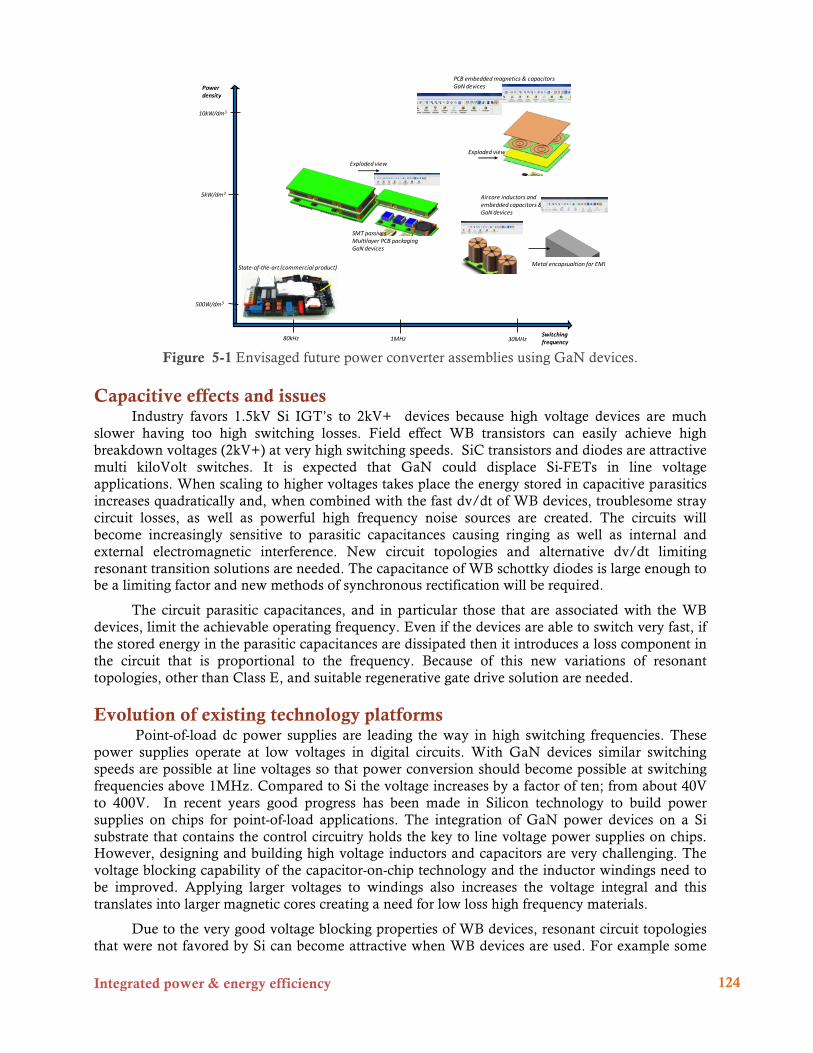
Integrated power & energy efficiency
124
Figure 5-1 Envisaged future power converter assemblies using GaN devices.
Capacitive effects and issues Industry favors 1.5kV Si IGT’s to 2kV+ devices because high voltage devices are much
slower having too high switching losses. Field effect WB transistors can easily achieve high breakdown voltages (2kV+) at very high switching speeds. SiC transistors and diodes are attractive multi kiloVolt switches. It is expected that GaN could displace Si-FETs in line voltage applications. When scaling to higher voltages takes place the energy stored in capacitive parasitics increases quadratically and, when combined with the fast dv/dt of WB devices, troublesome stray circuit losses, as well as powerful high frequency noise sources are created. The circuits will become increasingly sensitive to parasitic capacitances causing ringing as well as internal and external electromagnetic interference. New circuit topologies and alternative dv/dt limiting resonant transition solutions are needed. The capacitance of WB schottky diodes is large enough to be a limiting factor and new methods of synchronous rectification will be required.
The circuit parasitic capacitances, and in particular those that are associated with the WB devices, limit the achievable operating frequency. Even if the devices are able to switch very fast, if the stored energy in the parasitic capacitances are dissipated then it introduces a loss component in the circuit that is proportional to the frequency. Because of this new variations of resonant topologies, other than Class E, and suitable regenerative gate drive solution are needed.
Evolution of existing technology platforms Point-of-load dc power supplies are leading the way in high switching frequencies. These
power supplies operate at low voltages in digital circuits. With GaN devices similar switching speeds are possible at line voltages so that power conversion should become possible at switching frequencies above 1MHz. Compared to Si the voltage increases by a factor of ten; from about 40V to 400V. In recent years good progress has been made in Silicon technology to build power supplies on chips for point-of-load applications. The integration of GaN power devices on a Si substrate that contains the control circuitry holds the key to line voltage power supplies on chips. However, designing and building high voltage inductors and capacitors are very challenging. The voltage blocking capability of the capacitor-on-chip technology and the inductor windings need to be improved. Applying larger voltages to windings also increases the voltage integral and this translates into larger magnetic cores creating a need for low loss high frequency materials.
Due to the very good voltage blocking properties of WB devices, resonant circuit topologies that were not favored by Si can become attractive when WB devices are used. For example some
Power density
Switching frequency80kHz
500W/dm3
1MHz
5kW/dm3
10kW/dm3
30MHz
SMT passivesMultilayer PCB packagingGaN devices
PCB embedded magnetics & capacitorsGaN devices
State-‐of-‐the-‐art (commercial product)
Exploded view
Exploded view
Aircore inductors and embedded capacitors &GaN devices
Metal encapsualtion for EMI

Integrated power & energy efficiency
125
quasi resonant topologies exist where the semiconductor devices have to block voltages that could be two or more times larger than the input or output voltage. High step up ratios of dc converters can in theory be achieved at very high efficiency, which is important in applications such as photovoltaics.
SiC devices need to be packaged in power modules requiring new methods and technologes of hybrid integration. Since the SiC chips are very small, substantial heat spreading is needed which is not conducive for designing circuit layouts that minimize the loops that commutate the current between the power chips during switching. Due to the fast switching transients new ways have to be found to bring low inductance bus bars closer to the power chips. The fast dv/dts on the back sides of the chips will couple to other power chips in the module and the external heatsink. New power module layouts and mounting methods are needed to deal with the increased EMI threat.
Thermal challenges for GaN devices are much more severe than for Si devices, since the GaN devices are an order of magnitude smaller, yet only have a heat conductivity 3 times higher that Si.
Bridging the gap between power and RF electronics Best would be if a new packaging and circuit integration concept could be developed. Such a
concept would optimally place the switching and the electromagnetic energy storage and magnetic coupling functions in the three dimensional space while at the same time distribute the heat evenly. The conduction of heat and current could be done using an integral approach. A technology platform would be needed that gives more freedom to place the power devices, possible voltage and current sensors and to create and shape the electromagnetic fields associated with inductors, capacitors and transformers.
At frequencies approaching 100MHz, and when low loss magnetic and dielectric material would be available that have high relative permeabilities or permittivities, micro strip transmission line approaches may become relevant. At this point the distinction between power and RF electronics will begin to fade.
High temperature operation WB band gap devices can operate at higher temperatures than their Si counterparts which
useful for conversion systems that have to operate under extreme conditions. To fulfill the high temperature requirements not only the active switching devices need to withstand the elevated temperatures, but also the other components in the systems, passive components and sensors. Due to the limited availability of high temperature electromagnetic materials and consequently the smaller values of realizable inductors and capacitors and a smaller selection of sensors , it becomes necessary to find new circuit layout and topology solutions. For example, a converter could be split into two sub-circuits where the one contains the hot components and the other cold components.

Integrated power & energy efficiency
126
Gate drivers (co-integration) (GaN)
Jan Sonsky (NXP) With the contribution of:
Jean Jacques Aubert (CEA – Leti) Peter Moens (ONSemiconductor) Matthias Rose (NXP) Phil Rutter (NXP)
Abstract
The GaN-on-Si technology and components are lateral and thus has a potential to integrate multiple components or even full circuitry together with the power devices. The ultimate dream is to co-integrate drivers with the GaN power components on the same chip. This ambition is motivated by removing parasitic stray inductances and other parasitics, which is required to operate the power supplies at multi-MHz or even at multi-10s MHz frequencies. This section will discuss first differences in gate-driver requirements for Cascoded-GaN components vs. enhancement mode GaN devices.
Secondly different approaches being investigated by academia for monolithic integration of driver circuitry with GaN power devices will be outlined. Examples are building logic circuitry directly in GaN by means of advanced epitaxy and local removal of the selected layers to allow optimized islands for logic N-type transistor and logic P-type transistor. Other approach is based on building logic circuitry in the Si-carrier wafer and perform wafer bonding with GaN-layers.
Finally, heterogenous integration approaches using multiple dies in a single package will be discussed. To conclude, advantages and limitations of each approach will be sketched.
GaN gate driver requirements
Driver requirements for cascode GaN transistors Figure 5-2 shows the well known approach of a series connection of a normally-on (MGaN)
and a normally-off (MSi) power switch in a cascode configuration. This approach is becoming more and more popular for power electronic applications as new GaN (gallium nitride) power semiconductors with superior device characteristics compared to Silicon based switches are emerging into the market.
Basic GaN power semiconductors are depletion mode (normally-on) devices. Attempts to introduce additional layers in the layer stack of the power semiconductor to make the device normally-off come together with device performance penalties. Therefore cascoding high-voltage GaN switches with conventional low-voltage silicon trench MOSFETs is a viable option to combine the advantages of Silicon and GaN power devices.
To be able to benefit from the performance potential of GaN the drivers need to support their specific behavior. Applications using wide band gap transistors will tend toHigher efficiency,
- Higher switching frequencies, - Higher operating voltages and - More toward hard switching operation.

Integrated power & energy efficiency
127
Figure 5-2 Cascode configuration of a normally-on (MGaN) and a normally-off (MSi) power switch
This will lead in many cases toward optimized gate drivers for these kind of switches. But when considering driver circuits for GaN cascode switches, there is more than one solution. In Figure 5-3 the most prominent cascode configurations are depicted that are partly known from SiC cascode transistors already.
When considering the depicted GaN cascode switch configurations, there are basically two different ways to drive a cascode:
(1) The MOSFET MSi is driven directly by a gate driver and the GaN HEMT MGaN is controlled by the MOSFET drain-to-source voltage.
(2) The MOSFET MSi and the GaN HEMT MGaN are directly driven by two separate gate drivers. (active HEMT control)
In case of an active HEMT control, the two driver stages must be combined in a single driver circuit. New features are e.g. a negative driver supply, a synchronized turn-on/off behavior of the two switches to avoid over-voltages across the MOSFET and other cascode specific safety features.
Figure 5-3 GaN cascode HEMT alternatives

Integrated power & energy efficiency
128
Driver requirements for enhancement mode GaN transistors When defining the requirements for a e-mode GaN transistor, one need to distinguish
between an insulated gate and a Schottky gate transistor. These two device types require different driver circuit features. The main differences between these drivers are shown in Figure 5-4.
Figure 5-4 Basic gate driver cell to support GaN applications
In Figure 5-4 a basic gate driver cell is depicted. When considering to design such a gate driver cell specifically for GaN e-modes transistor then the following requirements need to be fulfilled:
- The driver core should have o gate protection against over-current and over-voltage, o a possibility to operate at a low gate voltage swing (reduced driver losses) o a low delay mismatch between digital input and driver output and o separate sink and source outputs to adjust turn-on and turn-off behavior separately.
- The driver supply should have o an active overvoltage clamp circuit or o a stable integrated driver supply regulator.
- The under-voltage lockout (UVLO) should be designed for o low driver supplies with narrow UVLO limits.
- The level shifter has to assist o high dv/dt level shifting.
All these requirements are defined considering the nature of GaN transistors to switch faster than comparable MOSFET counterparts. Therefore, a GaN specific gate driver mainly needs to support device operation at higher switching frequencies.
Additional GaN specific driver requirements can be defined when considering a half-bridge gate driverge driver circuit are:
- An extended basic driver cell that includes o de-saturation protection to protect the GaN device in case of over-current or short-
circuit conditions, o an active miller clamp to prevent the GaN device from self-turn-on and o integrated gate voltage wave shaping methods to improve the EME behavior.
- In order to enable high frequency operation, the driver should offer o high band width level shifters, o embedded DC/DC driver supply to reduce driver losses and o an adaptive dead time control to reduce free-wheeling losses.

Integrated power & energy efficiency
129
Monolithic integration approaches The monolithic integration of GaN power devices with logic circuitry allows number of
performance advantages and new application implementations. The key performance and functionality advantages include
• Device oscillation control and voltage overshoot limitation • Reduced stray parasitics to gate driver • Efficiency improvements and higher operating frequency • Reduced output capacitance due to less parasitic bondpads • Reduced stray inductances due to on-chip connection between multiple power devices
On application level, integration of power GaN stages with CMOS based ICs will allow for example supply current distribution over long-distance on CMOS chip at higher voltage (and lower total current) with local down-conversion using DC:DC converters based on GaN operating at much higher frequencies (100MHz). This will enable significant reduction in current consumption and related distribution losses.
It is expected that such integration will proceed in a few sequential steps. Initially, controlling circuitry such as resistors, diodes or logic-transistors will be incorporated in gate-lines of power transistors, see example in In Figure 5-5 [Boyi2011]. These additional circuit elements are already used to limit overshoot voltages and oscillations, and related losses for high-frequency power switching in lateral Si-power devices. Similar approach will be adopted also for lateral GaN technology.
Figure 5-5 Example of lateral power-Si devices and integrated on-chip circuitry (red elements) for NexFET power technology developed by TI [Boyi2011].
Next step will be half-bridge or full inverter on-chip integration as shown in Figure 5-6. Key benefits are in reducing total foot-print, reducing stray inductances and reducing bondpad capacitances.
The following steps will consists of a full-scale on-chip integration of GaN power devices with CMOS logic. This will allow full driver + power-stage on-chip integration as well as integration of different functionalities. There are two conceptually different approaches being under investigation.

Integrated power & energy efficiency
130
Figure 5-6 Example of 3-phase inverter stage integration on a single chip [Uemoto2009].
First approach is based on realizing low-voltage logic n-type and p-type transistors in GaN alongside power-stage devices. Technical realisation of this concept can be based on multi-epitaxial layer structure that comprises layers required to realize the different devices. Layers required to support logic N/P-transistors are realized in top of the structure, while layers required for high-voltage devices are located in lower part of the epitaxy. Subsequently, local removal of selected layers is used to create islands suitable for each component. Sketch of this approach is shown in Figure 5-7. Key challenges and limitations of this approach include
• Complex epitaxy growth • Realization of p-type logic device in GaN • Competitive performance of logic components • Reusability of standard logic, analog etc circuit blocks
Figure 5-7 Monolithic Integration of different electronic and optical devices in single GaN chip [Chow2011]
The second monolithic integration approach is based on wafer bonding of GaN-on-Si wafers with SOI wafer [Chung2009], see Figure 5-8. Using further wafer-bonding and Si-backgrinding technology results in wafer comprising Si-SiO2-GaN-Si that can be used as starting material for IC manufacturing comprising both CMOS and GaN-specific technological steps. Key advantage of this approach is that logic/analog components are build in Si using standard and known manufacturing processes. Key challenges includes
• Multiple wafer bonding • CMOS build in a relatively thin Si-layer • Compatibility of CMOS manufacturing with GaN
CMOS LEDHV FETs

Integrated power & energy efficiency
131
Figure 5-8 Monolithic integration of Si-CMOS and GaN-power components [Chung2009].
Heterogenous integration Prior to monolithic integration, it is expected that GaN based products will be dominated by
multi-chip modules comprising for example
• GaN die + Si LVMOS die (Cascode) • GaN die + Si LVMOS die (Cascode) + driver die • GaN die (E-mode) + driver die
The one package approach for Cascode implementation is required to minimize critical parasitic inductance of the connection between GaN source and LVMOS drain. The advantages of driver co-integration in a single package with either Cascode or E-mode GaN device becomes more prominents at higher operating frequency (above 1MHz).
GaN drivers and GaN co-integration, key topics & requirements for future funded projects • Strong combination of driver/appl and device architecture • Technologies (epitaxy, process) enabling complementary devices, i.e. also P-channel • High-freq. & efficient driver designs • Technologies exploring advanced cooling • Technologies for substrate engineering and integrated passives • Packaging and Assembly approaches with reduced inductances & good heat-sinking References [Boyi2011] Boyi Yang et al., “NexFET Generation 2, New Way to Power”, IEDM 2011
proceeding, pp. 583-586. [Uemoto2009] Yasuhiro Uemoto et al., “GaN Monolithic Inverter IC Using Normally-off Gate
Injection Transistors with Planar Isolation on Si Substrate”, IEDM2009 proceeding, pp. 165-168.
[Chow2011] T. Paul Chow et al., “Recent advances and Commercialization of SiC and GaN Devices”, CPES seminar 2011
[Chung2009] Jinwook W. Chung et al., “Seamless On-Wafer Integration of Si(100) MOSFETs and GaN HEMTs”, IEEE EDL 30 (10), 2009, pp. 1015-1017

Integrated power & energy efficiency
132
Thermal design and thermal management
Jelena Popovic (TU Delft) With the contribution of:
Braham Ferreira (TU Delft) Tomas Harder (ECPE) Daan van Wyk (UJ)
Abstract The implementation of WBG devices in power electronic converters requires new thermal
management approaches for the following reasons:
- For the same power rating the cross sectional area of the dies is substantially reduced. To remove the same amount of losses more and better heat spreading is needed.
- The devices are able to operate at higher temperatures so that larger thermal resistances could be tolerated.
- There is a trade-off between a high frequency operation and good thermal management in WBG converter. For fast switching the components have to be placed close to each other to minimize parasitics reducing the area for heat spreading. The capacitive coupling between the heat spreaders and heat sink impairs a high frequency operation.
- There is a change in the power loss distribution between active and passive components in WBG power converters. Power semiconductors are not necessarily the largest contributors to the total losses in WBG converters.
- High frequency operation leads to miniaturization of electrically active parts of the converter, especially passives. The volume of thermal management parts, however, could take up a significant portion of the total volume.
- The packages suitable for high frequency operation require surface mount assembly and are unsuitable for large volume consumer applications.
Spreading the heat of small WBG dies For the same power rating the surface area of WBG dies is several times smaller than that of
their silicon counterparts. In order to remove the heat from these devices, better heat spreading is needed. Furthermore, in the case of GaN devices the low thermally conductivity of Si and the influence of the thermal resistance of the transitional buffer layer makes the situation worse. Better heat spreading solutions are needed on both die and assembly level. On the die level approaches such as integrating more devices into one die for lateral GaN devices, removing the Si substrate or integrating microchannel coolers are some of the possibilities.
The conventional design rules for heat spreading on PCBs are no longer valid. Increasing the size of the heat spreader is not enough, better materials and more advanced substrate designs have to be used. In the case of discrete packaged devices, heat spreaders made of materials with anisotropic thermal conductivities such as composite materials used in RF power packaging should be investigated. For bare dies packaged on a substrate (power module or a PCB) designs with multilayer heat spreading and high thermal conductivity substrates are needed. Assembly technologies allowing for double sided heat removal where both sides considerably contribute to the heat removal are the most desirable. These could include planar metallization and assembly technologies in power modules or 3D stacking of power devices.

Integrated power & energy efficiency
133
In the case of GaN devices it is desirable to utilize the top side of the die for heat removal due to the lower thermal resistance and omitting the transitional buffer layer resistance (which can be as high as 30% of the total thermal resistance for GaN-on-Si and even more for SiC substrates). However, the thermal resistance of the available interconnection technologies such as flip chip solder bumps is several times larger than that of the backside mounted device. Alternative top side interconnection technologies such as copper bumps and mounting technologies are needed. These technologies may have an influence on the metallization of the dies.
Thermal management vs. high frequency operation There are fundamental trade-offs between a high frequency operation of WBG power
electronic circuits and an effective thermal management if conventional design approaches are used. Large areas required for heat spreading are counter indicated to a high frequency operation of WBG converters. Components need to be placed close to each other in order to reduce parasitic inductances detrimental for fast switching of devices, which does not give much space for heat spreading. In order to achieve high frequency operation it will be desirable to place decoupling capacitors as close as possible to the devices, for e.g. preferably on top of the devices which will prohibit the use of the top side for heat removal. Furthermore, multilayer layout techniques for reducing parasitic inductance tend to increase parasitic capacitance. The capacitive coupling between the heat spreader of the devices (e.g. lead frame of a discrete package) and the heat sink is directly proportional to the surface area of the heat spreader and will be in the order of magnitude of the parasitic drain-source capacitance of the die or even larger which will significantly increase the losses at high frequency switching. Circuit topologies, heat spreading layouts and three dimensional physical designs (e.g. three dimensional stacking of power devices) that can handle these trade-offs will need to be developed. 3-D packaging removes constraints imposed by two dimensional lay-outs in terms of coupling heat removal and electromagnetic improvement in the design. Conduction losses in conductors at very high switching frequencies due to the skin effect and proximity effect can lead to the reduced current capability of conductors for the allowed temperature rise, requiring more effective cooling of conductors.
New thermal management design approaches Due to their fast switching, WBG devices enable power conversion at much higher switching
frequencies. This enables miniaturization of converters, especially through the reduction in the volume of passive components. The result can be that the thermal management parts take up considerable portion of the converter volume. More efficient approaches to thermal management such as the multifunctional use of converter parts (e.g. heat conduction, electrical interconnection, mechanical support) are needed.
Due to the limitations in heat spreading of WBG devices, more modular based converter architectures where heat is distributed over multiple sources can be desirable. This can be reinforced with the benefit of having each cell or module operate under a narrow range of operating conditions thus allowing a high efficiency operation. In order to get the full benefit of the use of these WBG switches the existing approaches are insufficient. New mechanical (and partly electrical) technologies are to be investigated thoroughly.
Three general approaches for exploiting WBG devices from the thermal point of view are possible: • The devices run at moderate temperature to improve reliability. This imposes the need for
optimizing heat transfer from the die to the heat removal devices (pcb, substrate, heatsink ..) • Both devices and substrate running at high temperature. This gain needs a low thermal
resistivity between die and substrate, but imposes a burden on the connecting technology, as that will have to sustain quite some thermal stress.
• The device runs at high temperature, while the other parts of the circuit are still running at moderate temperature.

Integrated power & energy efficiency
134
High temperature operation In case of WBG devices operating at much higher temperatures compared to the rest of the
parts in a power converter assembly, the thermo-mechanical behaviour of the assembly will be different. Since the thermo-mechanical stresses are proportional to the differences in the expansion of materials which is a product of a CTE and ∆T the higher temperature excursion of semiconductors and lower CTE compared to lower temperature excursion and higher CTE of substrates may even be exploited to reduce thermal stresses. This will also involve the introduction of new interconnection technologies, as also for high temperature the connection must remains stable, and reliable, while maintaining low thermal and/or electrical resistance.
High temperature operation, alternative approach A traditional approach in thermal management is to reduce the thermal resistance of
semiconductor packages as much as possible in order to reduce the semiconductors’ operating temperatures. Since WBG devices can operate at much higher operating temperatures (~400C or higher) it can be envisaged that in some applications it may be beneficial to have a high thermal resistance package so that the semiconductor works at a higher temperature and the rest of the converter at lower temperatures.
Potential benefit of this approach is, that the high temperature capabilities of the WBG devices can be exploited fully, while maintaining relative low temperature of the surrounding components, thus improving their reliability and most often lowering the losses in these other components. It will also relieve the thermal stress in all parts, and on the connecting technologies, leaving less expensive (and partly more conventional, with proven reliability) technologies feasible..
Thermal management of passives Due to the low on-resistance and fast switching of WBG devices, the loss distribution among
active and passive devices in WBG converters will change and power semiconductors will not necessarily be the largest loss contributors as already illustrated in WBG converter prototypes in literature. This is especially the case for very high frequency operations where passive components become very lossy (e.g. in VHF power converter prototypes active components contribute less than 20% to the total loss). For this reason both new materials for passive components better suited for MHz operation need to be developed and new thermal management approaches for passive components on the component and on the converter level. These may include 3D heat spreading concepts, integrating thermally active parts in the construction of passive components and the use of new materials such as thermally conductive polymers for overmoulding and housing of passive components and whole sub-assemblies.
Market penetration Chip-size packages and interconnection technologies, such as flip chip packages (LBGA),
are preferred for high frequency operation due to their low parasitics. However, they require to be assembled with reflow soldering and need to be assembled on thermally enhanced substrates for heat removal. This is cost prohibitive in some applications (e.g. consumer) where only wave soldering and low performance PCBs are allowed. These applications could be crucial for large volume application of WBG devices, especially of GaN. For these applications, packages that can be mounted on a heat sink and wave soldered are required. This comes at a price of increased package parasitic. Alternative approaches are needed to fully exploit the potential of WBG devices in these applications.
A challenge for this market is to come with topologies (and/or control of switching behavior) that limits the negative consequences of these parasitic.

Integrated power & energy efficiency
135
EMC of power devices
Renaud Gillon (ONSemiconductor) With the contribution of:
Eckart Hoene (Fraunhofer-‐IZM) Peter Moens (ONSemiconductor) Joachim Pelka, (Fraunhofer VµE)
Abstract The electro-magnetic compatibility (EMC) of power devices, involves both the aspects of
their immunity to external unwanted signals, and the emissions of conducted and radiated interference signals. The final EMC performance of the power converter system is in both cases the result of interactions between the power device itself and its immediate “environment” usually schematically represented as the “loads” attached to its terminals.
Hence is the EMC performance of future power devices conditioned both by the features and limitations of power device technology itself, as well as those of the surrounding system components. The sensitivity of the EMC performance of the converter to particular features of the power devices and the surrounding components is itself modulated by the selected converter topology. Introduction of new technologies for the power device or for the other components that shift the performance trade-offs and enable new grounds in terms of energy efficiency, also create significant new opportunities and risks in terms of EMC. The current trend towards more compact and faster power devices will most likely impact the following effects :
• Susceptibility of the power devices to external perturbation, most often witnessed as unintentional turn-on or turn-off of the device during operation, (Bona & Fiori, 2011), which in some cases may lead to destruction. Higher gain and bandwidth of the power devices will require tighter design constraints on the surrounding network in order to maintain the immunity levels.
• Emission of conducted perturbances on the supplies. The smaller size and capacitances of the power devices will probably shift emission spectra to higher frequencies, which will likely facilitate the filtering, (Majid, Saleem, & Bertilsson, 2012). However as the frequencies rise, the location of the filtering elements will become more critical, and crowding might become an issue.
• Radiated emissions from magnetic sources caused by resonating current loops, (Bhargava A. , Pommerenke, Kam, Centola, & Lam, 2011). Higher oscillation frequencies will make structures more efficient antenna’s, so the risk of exceeding radiated emission levels might increase. However, increased frequencies could ease the shielding, as skin-depth becomes small with respect to conductor thicknesses.
• Radiated emissions from electric sources caused by oscillating voltages. Until now the main radiation risks in converters was related to magnetic type sources. With the advent of faster high-voltage capable devices, and the multiplication of direct mains conversion applications, the risk of emissions from electric-type antenna’s will likely increase, calling for additional shielding measures. The typical structure of GaN HEMT devices with the floating substrate presents a challenge in this respect, as signals from fast switching electrodes (drain) can couple capacitively to the substrate and eventually couple into such structures as heat-sinks and radiate.

Integrated power & energy efficiency
136
Publications about realizations of high-frequency power converters relying on GaN HEMT power transistors show that radiated emissions are indeed becoming a source of concerns, and that package design as well as substrate or module layouts must be carefully optimized in order to keep radiated emissions at acceptable levels, (Delaine, Jeannin, Frey, & Guepratte, 2012).
In order to enable the effective deployment of high-frequency GaN-based power converters, it is essential to address EMC risks related to this family of new applications in a cost-effective manner. A series of gaps can be identified in relation with the key EMC effects described earlier, which unless addressed will hamper the development of GaN-based power converters by exacerbating the EMC risks or the costs related to their mitigation. Hence future research should allow to target the following objectives :
• Availability of low-profile packages allowing to minimize inductances and reduce the area of possible resonance loops which could act as radiating magnetic dipoles.
• Availability of packages which in the case of high-voltage switching provide sufficient shielding in order to avoid coupling harmonics capacitively to neighbouring structures which could radiate.
• Substrates with thin dielectric layers offering a maximum of decoupling capacitances but also allowing to obtain maximum cancellation of resonance currents by their images in a nearby ground conductor.
• Ability to co-integrate de-coupling or tuning elements like capacitors, resistors or diodes along with the power transistor, either on-chip or in the package
• Availability of electro-magnetic simulation technology capable of handling the complexity of the full geometry of a power converter module, in order to identify resonances and compute the loads seen by the power transistor over a broad range of frequencies
• Availability of power transistor models allowing to not only account for the current-voltage characteristics, but also deal with the distributed nature of such effects as self-heating, signal propagation delays along electrodes and impact of current-crowding induced by external magnetic fields
• Ability to probe high-frequency currents and voltages with high fidelity (no delay, distortion, attenuation, etc.) at PCB level or inside modules.
References
[1] C. Bona and F. Fiori, "MOS power transistor model for Electromagnetic Susceptibility analysis," Microelectronics Reliability, vol. 51, no. 8, pp. 1356-1364, 2011. [Online]. http://www.sciencedirect.com/science/article/pii/S0026271411000795
[2] A. Majid, J. Saleem, and K. Bertilsson, "EMI filter design for high frequency power converters," in Environment and Electrical Engineering (EEEIC), 2012 11th Int. Conference on, may 2012, pp. 586-589.
[3] A. Bhargava, D. Pommerenke, K.W. Kam, F. Centola, and Cheng Wei Lam, "DC-DC Buck Converter EMI Reduction Using PCB Layout Modification," Electromagnetic Compatibility, IEEE Transactions on, vol. 53, no. 3, pp. 806-813, Aug. 2011.
[4] J. Delaine, P.-O. Jeannin, D. Frey, and K. Guepratte, "High frequency DC-DC converter using GaN device," in Applied Power Electronics Conference and Exposition (APEC), 2012 Twenty-Seventh Annual IEEE, feb. 2012, pp. 1754-1761.
[5] Peng Shao, F. Chang, C. Reade, P. Ilavarasan, and D. Pommerenke, "Finding return current paths via synchronized measurements in a multiphase DCDC buck converters," in Electromagnetic Compatibility, 2009. EMC 2009. IEEE International Symposium on, aug. 2009, pp. 53-57.
[6] K. Shah and K. Shenai, "Performance Evaluation of Point-of-Load Chip-Scale DC-DC Power Converters Using Silicon Power MOSFETs and GaN Power HEMTs," in Green Technologies Conference (IEEE-Green), 2011 IEEE, april 2011, pp. 1-5.

Integrated power & energy efficiency
137
[7] Ming-Jen Pan and C.A. Randall, "A brief introduction to ceramic capacitors," Electrical Insulation Magazine, IEEE, vol. 26, no. 3, pp. 44-50, May-June 2010.
[8] I. Omura, W. Saito, T. Domon, and K. Tsuda, "Gallium Nitride power HEMT for high switching frequency power electronics," in Physics of Semiconductor Devices, 2007. IWPSD 2007. International Workshop on, dec. 2007, pp. 781-786.
[9] K. Matsuura, H. Yanagi, S. Tomioka, and T. Ninomiya, "Power-density development of a 5MHz-switching DC-DC converter," in Applied Power Electronics Conference and Exposition (APEC), 2012 Twenty-Seventh Annual IEEE, feb. 2012, pp. 2326-2332.
[10] Reinel Marante, M. Nieves Ruiz, Leysi Rizo, Lorena Cabria, and Jose A. Garcia, "A UHF class E2 DC/DC converter using GaN HEMTs," in Microwave Symposium Digest (MTT), 2012 IEEE MTT-S International, june 2012, pp. 1-3.
[11] Zhe Li and D. Pommerenke, "EMI specifics of synchronous DC-DC buck converters," in Electromagnetic Compatibility, 2005. EMC 2005. 2005 International Symposium on, vol. 3, aug. 2005, pp. 711 - 714 Vol. 3.
[12] Hongyu Li et al., "Conducted EMI simulation of switched mode power supply," in Electromagnetic Compatibility, 2009. EMC 2009. IEEE International Symposium on, aug. 2009, pp. 155-160.
[13] H.B. Kotte, R. Ambatipudi, and K. Bertilsson, "High speed cascode flyback converter using multilayered coreless printed circuit board (PCB) step-down power transformer," in Power Electronics and ECCE Asia (ICPE ECCE), 2011 IEEE 8th International Conference on, 30 2011-june 3 2011, pp. 1856-1862.
[14] Keong Kam et al., "Quantification of Self-Damping of Power MOSFET in a Synchronous Buck Converter," Electromagnetic Compatibility, IEEE Transactions on, vol. 53, no. 4, pp. 1091-1093, nov. 2011.
[15] K.W. Kam, D. Pommerenke, Cheung-Wei Lam, and R. Steinfeld, "EMI analysis methods for synchronous buck converter EMI root cause analysis," in Electromagnetic Compatibility, 2008. EMC 2008. IEEE International Symposium on, aug. 2008, pp. 1-7.
[16] J. A. Garcia, R. Marante, and M. de las Nieves Ruiz Lavin, "GaN HEMT Class Resonant Topologies for UHF DC/DC Power Conversion," Microwave Theory and Techniques, IEEE Transactions on, vol. PP, no. 99, pp. 1-10, 2012.
[17] S. Dargahi, P. Valizadeh, and S.S. Williamson, "Proof-of-concept gallium-nitride power electronic converter design for HEV energy management application," in Vehicle Power and Propulsion Conference (VPPC), 2011 IEEE, sept. 2011, pp. 1-5.
[18] Wanjun Chen, King-Yuen Wong, and K.J. Chen, "Monolithic integration of lateral field-effect rectifier with normally-off HEMT for GaN-on-Si switch-mode power supply converters," in Electron Devices Meeting, 2008. IEDM 2008. IEEE International, dec. 2008, pp. 1-4.
[19] A. Bhargava et al., "EMI prediction in switched power supplies by full-wave and non-linear circuit co-simulation," in Electromagnetic Compatibility, 2009. EMC 2009. IEEE International Symposium on, aug. 2009, pp. 41-46.
[20] M. Acanski, J. Popovic-Gerber, and J.A. Ferreira, "Comparison of Si and GaN power devices used in PV module integrated converters," in Energy Conversion Congress and Exposition (ECCE), 2011 IEEE, sept. 2011, pp. 1217-1223.