integrated photonic beamformer employing
DESCRIPTION
Integrated photonic beamformer employing continuously tunable ring resonator-based delays in CMOS-compatible LPCVD waveguide technology. C. G. H. Roeloffzen* a , A. Meijerink a , L. Zhuang a , D. A. I. Marpaung a , R. G. Heideman b , A. Leinse b , M. Hoekman b , W. van Etten a . - PowerPoint PPT PresentationTRANSCRIPT
1 / 32
Integrated photonic beamformer employing continuously tunable ring resonator-based
delays in CMOS-compatible LPCVD waveguide technology
C. G. H. Roeloffzen*a, A. Meijerinka, L. Zhuanga, D. A. I. Marpaunga, R. G. Heidemanb, A. Leinseb, M. Hoekmanb, W. van Ettena.
aUniversity of Twente, Faculty of Electrical Engineering, Mathematics and Computer Science, Telecommunication Engineering Group, P.O. Box 217, 7500 AE Enschede, The Netherlands bLioniX B.V., P.O. Box 456, 7500 AH Enschede, The Netherlands
2 / 30MWP » MWP in PAAs » SMART » Conclusions » Questions
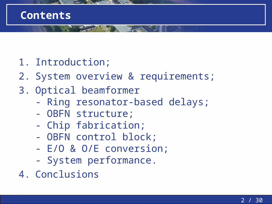
Contents
1. Introduction;
2. System overview & requirements;
3. Optical beamformer- Ring resonator-based delays;- OBFN structure;- Chip fabrication;- OBFN control block;- E/O & O/E conversion;- System performance.
4. Conclusions
3 / 46MWP » MWP in PAAs » SMART » Conclusions » Questions »
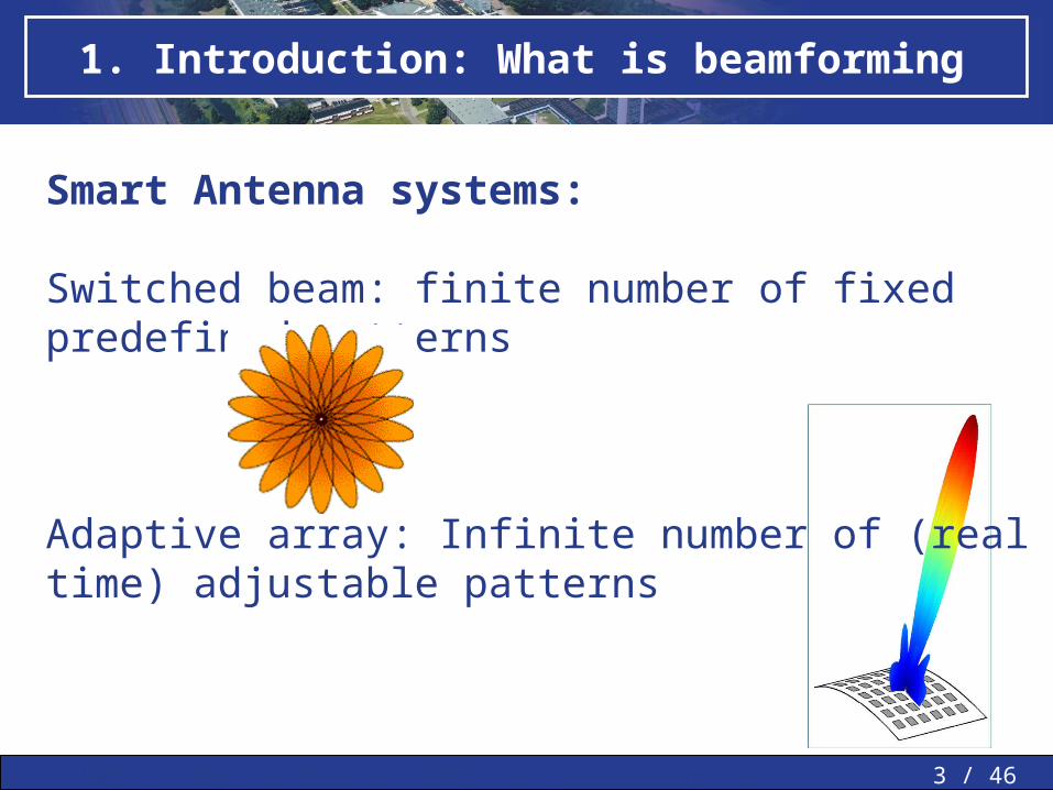
1. Introduction: What is beamforming
Smart Antenna systems:
Switched beam: finite number of fixed predefined patterns
Adaptive array: Infinite number of (real time) adjustable patterns
4 / 46MWP » MWP in PAAs » SMART » Conclusions » Questions »
1. Introduction: Smart antenna
Smart Antenna systems:
Using a variety of new signal-processing algorithms, the adaptive system takes advantage of its ability to effectively locate and track various types of signals to dynamically minimize interference and maximize intended signal reception.
Beamforming: spatial filtering
5 / 46MWP » MWP in PAAs » SMART » Conclusions » Questions »
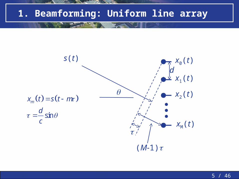
1. Beamforming: Uniform line array
x0(t)d
x1(t)
x2(t)
xM(t)
s(t)
(M-1)
sin
mx t s t m
d
c
6 / 46MWP » MWP in PAAs » SMART » Conclusions » Questions »
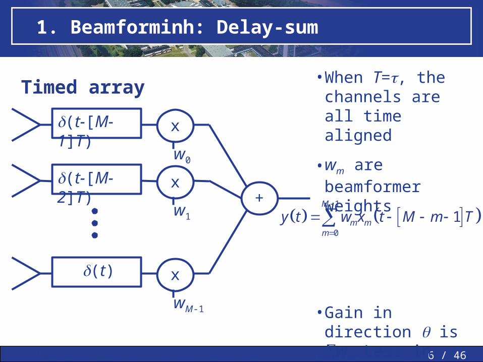
1. Beamforminh: Delay-sum
Timed array
+
(t-[M-1]T)
(t-[M-2]T)
(t)
w0
x
w1
x
wM-1
x
• When T=, the channels are all time aligned
• wm are beamformer weights
• Gain in direction is wm. Less in other directions due to incoherent addition.
1
0
1M
m mm
y t w x t M m T
7 / 46MWP » MWP in PAAs » SMART » Conclusions » Questions »
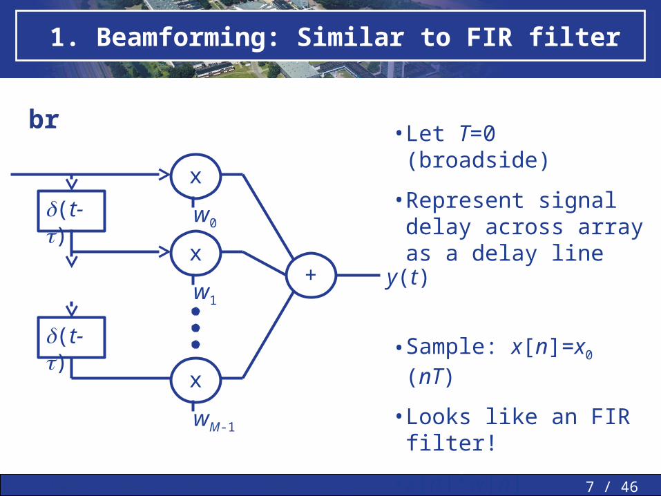
1. Beamforming: Similar to FIR filter
br
+
w0
x
w1
x
wM-1
x
• Let T=0 (broadside)
• Represent signal delay across array as a delay line
• Sample: x[n]=x0 (nT)
• Looks like an FIR filter!
• x[n]*w[n]
• Design w with FIR methods
(t-)
(t-)
y(t)
8 / 46MWP » MWP in PAAs » SMART » Conclusions » Questions »
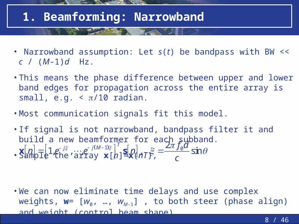
1. Beamforming: Narrowband
• Narrowband assumption: Let s(t) be bandpass with BW << c / (M-1)d Hz.
• This means the phase difference between upper and lower band edges for propagation across the entire array is small, e.g. < /10 radian.
• Most communication signals fit this model.
• If signal is not narrowband, bandpass filter it and build a new beamformer for each subband.
• Sample the array x[n]=x(nT),
• We can now eliminate time delays and use complex weights, w= [w0, …, wM-1] , to both steer (phase align) and weight (control beam shape)
1 021, , , , sin
Tj Mj f d
n e e nc
x s
9 / 46MWP » MWP in PAAs » SMART » Conclusions » Questions »
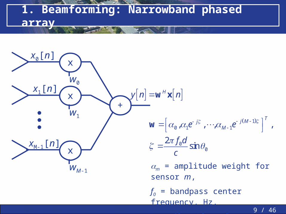
1. Beamforming: Narrowband phased array
+
w0
x
w1
x
wM-1
x
m = amplitude weight for sensor m,
f0 = bandpass center frequency, Hz,
0 = direction of max response
x0[n]
x1[n]
xM-1[n]
Hy n nw x
10 1 1
00
, , , ,
2sin
Tj MjMe e
f d
c
w
10 / 46MWP » MWP in PAAs » SMART » Conclusions » Questions »
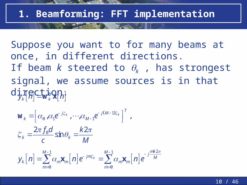
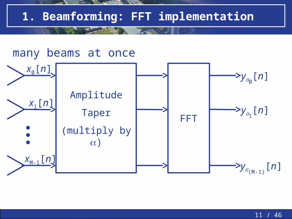
1. Beamforming: FFT implementation
Suppose you want to for many beams at once, in different directions.If beam k steered to k , has strongest signal, we assume sources is in that direction.
Hk ky n nw x
10 1 1
0
, , , ,
2 2sin
kkTj Mj
k M
k k
e e
f d k
c M
w
21 1
0 0
k
mkM M jjm Mk m m m m
m m
y n n e n e
x x
11 / 46MWP » MWP in PAAs » SMART » Conclusions » Questions »
1. Beamforming: FFT implementation
many beams at oncex0[n]
x1[n]
xM-1[n]
Amplitude
Taper
(multiply by )
FFT
y0[n]
y1[n]
y(M-1)[n]
12 / 46MWP » MWP in PAAs » SMART » Conclusions » Questions »
1. Beamforming: Examples
Beamforming:
Electronic
Digital
Optical
13 / 46MWP » MWP in PAAs » SMART » Conclusions » Questions »
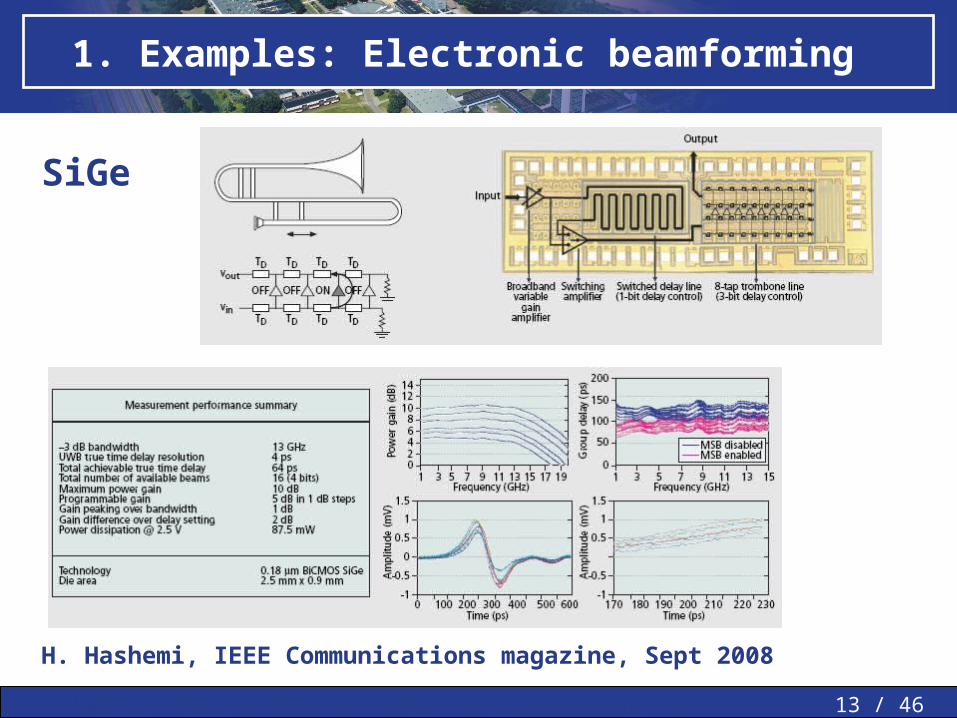
1. Examples: Electronic beamforming
SiGe
H. Hashemi, IEEE Communications magazine, Sept 2008
14 / 46MWP » MWP in PAAs » SMART » Conclusions » Questions »
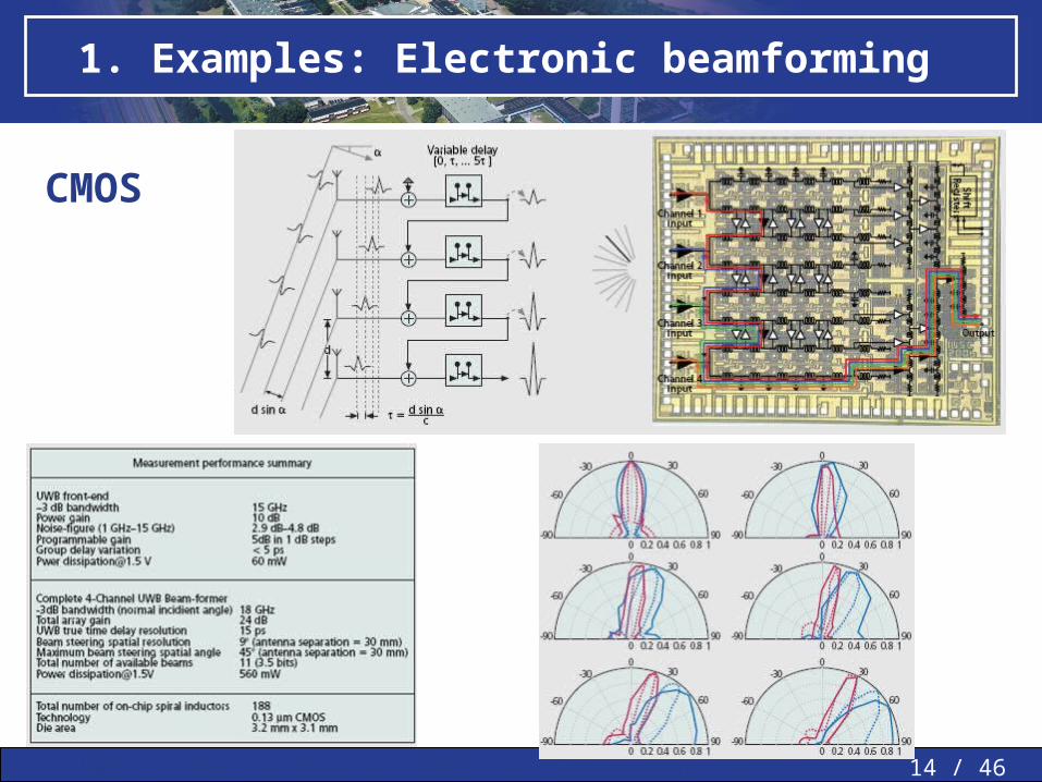
1. Examples: Electronic beamforming
CMOS
15 / 46MWP » MWP in PAAs » SMART » Conclusions » Questions »
1. Examples: Electronic beamforming
MMIC (CMOS & SiGe)
+ very small chip+ TTD & phase shifters- Switched delay+ Large bandwidth+ low power consumption- Large coupling between channels
16 / 46MWP » MWP in PAAs » SMART » Conclusions » Questions »
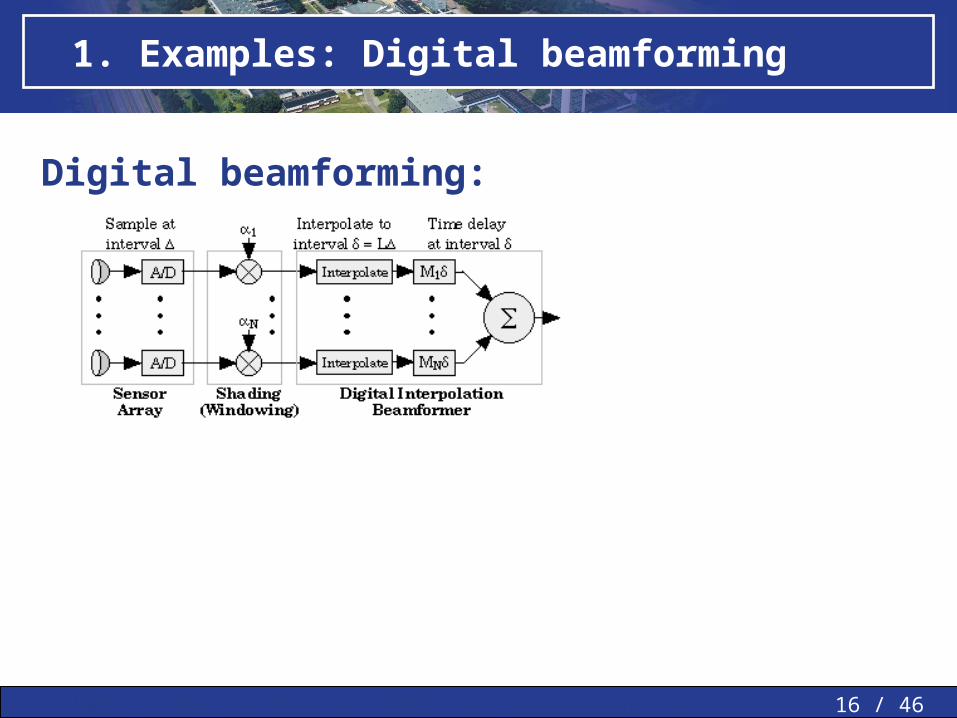
1. Examples: Digital beamforming
Digital beamforming:
17 / 46MWP » MWP in PAAs » SMART » Conclusions » Questions »
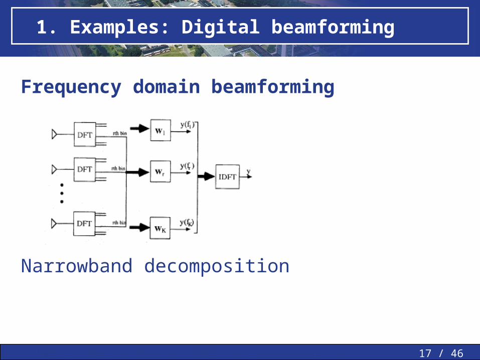
1. Examples: Digital beamforming
Frequency domain beamforming
Narrowband decomposition
18 / 46MWP » MWP in PAAs » SMART » Conclusions » Questions »
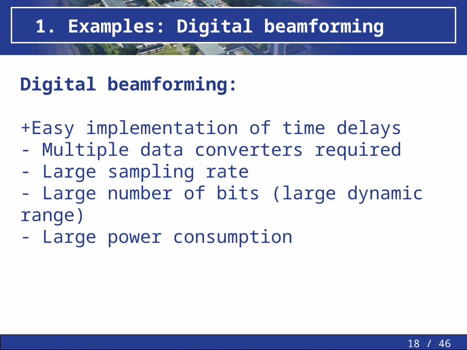
1. Examples: Digital beamforming
Digital beamforming:
+Easy implementation of time delays- Multiple data converters required- Large sampling rate- Large number of bits (large dynamic range)- Large power consumption
19 / 46MWP » MWP in PAAs » SMART » Conclusions » Questions »
1. Examples: Optical beamforming
Optical beamforming:
+Easy

20 / 46MWP » MWP in PAAs » SMART » Conclusions » Questions »
1. Int: aose
Smart
21 / 46MWP » MWP in PAAs » SMART » Conclusions » Questions »
1. Introduction: aim and purpose
Aim:
Development of a novel Ku-band antenna for airborne reception of satellite signals
Purpose:• Live weather reports;• High-speed Internet access;• Live television through Digital Video
Broadcasting via satellite (DVB-s)
, using a broadband conformal phased array
22 / 46MWP » MWP in PAAs » SMART » Conclusions » Questions »
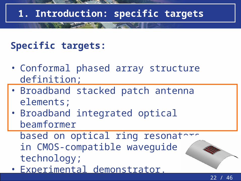
1. Introduction: specific targets
Specific targets:
• Conformal phased array structure definition; • Broadband stacked patch antenna elements;• Broadband integrated optical beamformer
based on optical ring resonatorsin CMOS-compatible waveguide technology;
• Experimental demonstrator.
23 / 46MWP » MWP in PAAs » SMART » Conclusions » Questions »
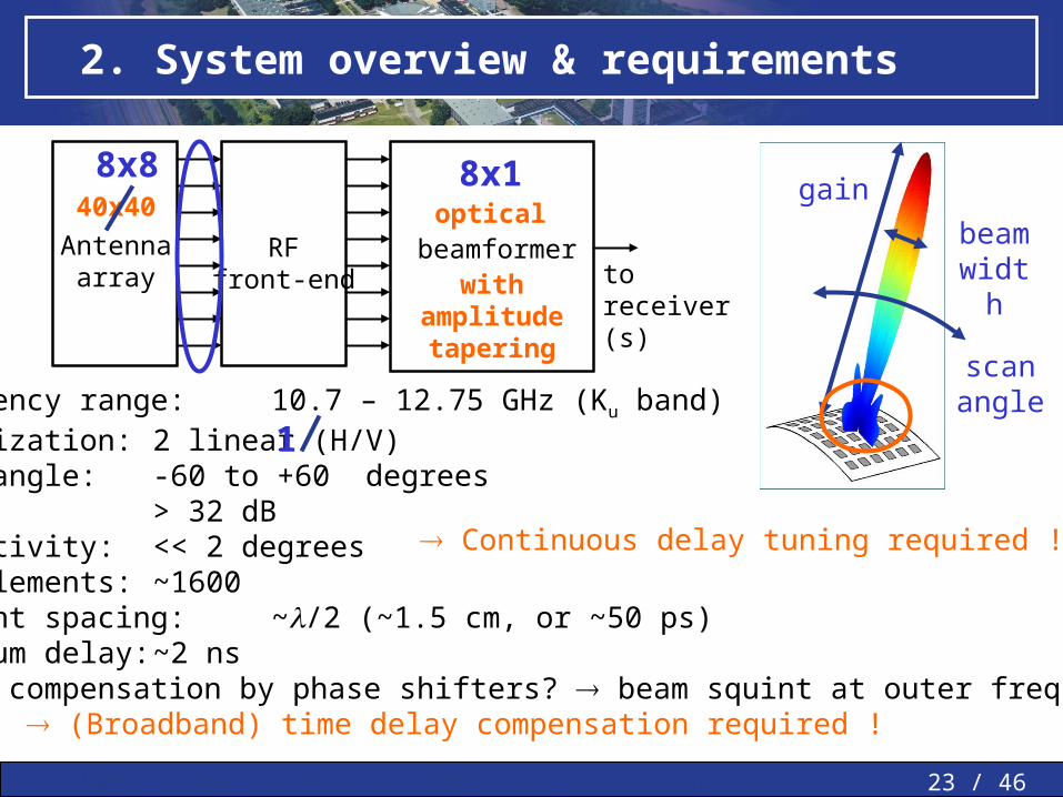
2. System overview & requirements
beamformerAntennaarray
RFfront-end to
receiver(s)
Frequency range: 10.7 – 12.75 GHz (Ku band)Polarization: 2 linear (H/V)Scan angle: -60 to +60 degreesGain: > 32 dBSelectivity: << 2 degreesNo. elements: ~1600Element spacing: ~/2 (~1.5 cm, or ~50 ps)Maximum delay: ~2 nsDelay compensation by phase shifters? beam squint at outer frequencies! (Broadband) time delay compensation required !
40x40
Continuous delay tuning required !
gain
beam width
scan angle
optical
with amplitude tapering
8x8
1
8x1
24 / 46MWP » MWP in PAAs » SMART » Conclusions » Questions »
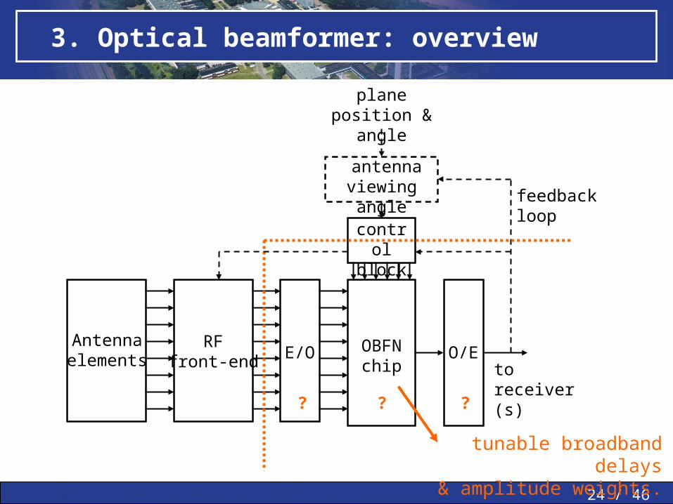
3. Optical beamformer: overview
OBFN chip
Antennaelements
RFfront-end to
receiver(s)
E/O O/E
? ?
tunable broadband delays& amplitude weights.
?
controlblock
antenna viewing angle
plane position & angle
feedbackloop
25 / 46MWP » MWP in PAAs » SMART » Conclusions » Questions »
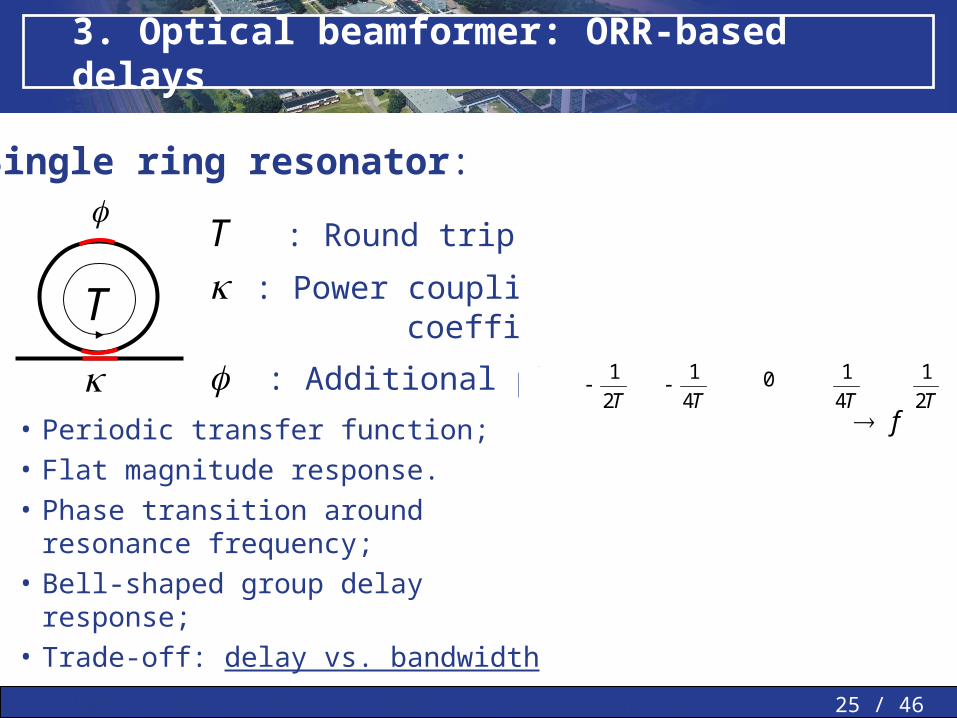
3. Optical beamformer: ORR-based delays
T
T4
1 0
T4
1
T2
1
2
T8
T4
T2
T6
0
2.1
T10
6.1
0
T2
1
8.0
4.0
f
Gro
up
d
ela
y
P
has
e
TFSR
1
Single ring resonator:
T : Round trip time;
: Power coupling coefficient;
: Additional phase.
• Periodic transfer function;• Flat magnitude response.• Phase transition around
resonance frequency;• Bell-shaped group delay response;• Trade-off: delay vs. bandwidth
T4
1 0
T4
1
T2
1
T2
1
f
26 / 46MWP » MWP in PAAs » SMART » Conclusions » Questions »
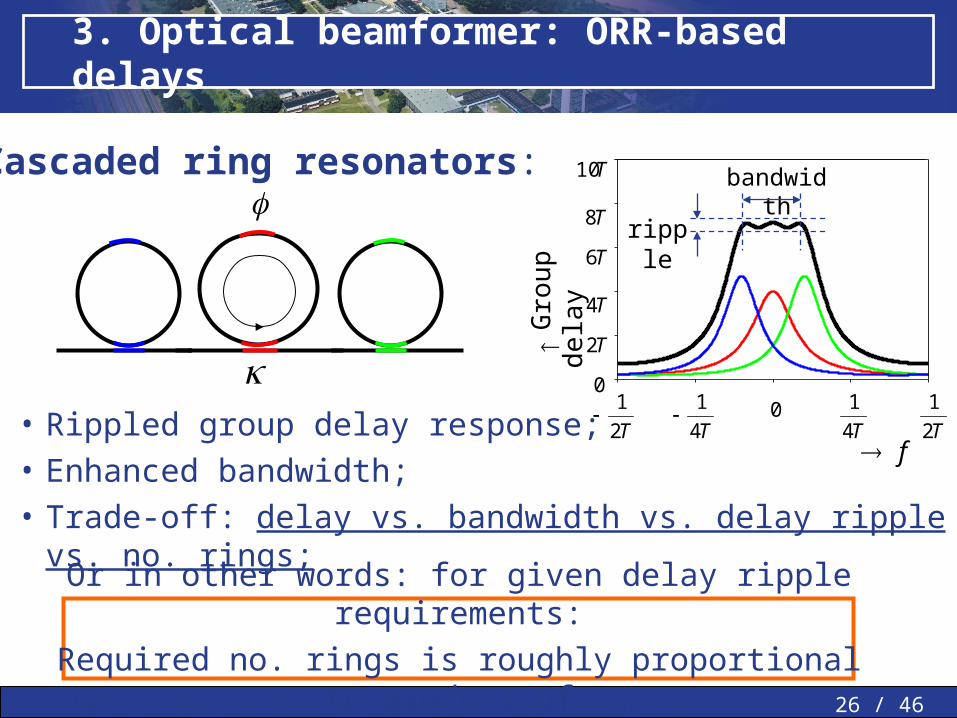
3. Optical beamformer: ORR-based delays
Cascaded ring resonators:
• Rippled group delay response;• Enhanced bandwidth;• Trade-off: delay vs. bandwidth vs. delay ripple vs. no. rings;
ripple
bandwidth
T4
1 0
T4
1
T2
1
T2
1
f
T8
T4
T2
T6
0 G
rou
p
del
ay
T10
Or in other words: for given delay ripple requirements:
Required no. rings is roughly proportional to product of required optical bandwidth and maximum delay
27 / 46MWP » MWP in PAAs » SMART » Conclusions » Questions »
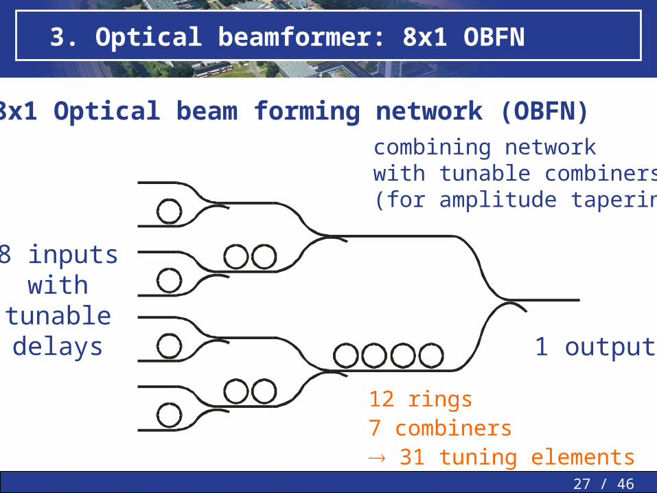
3. Optical beamformer: 8x1 OBFN
8x1 Optical beam forming network (OBFN)
8 inputswith
tunabledelays 1 output
combining networkwith tunable combiners(for amplitude tapering)
12 rings7 combiners 31 tuning elements
28 / 46MWP » MWP in PAAs » SMART » Conclusions » Questions »
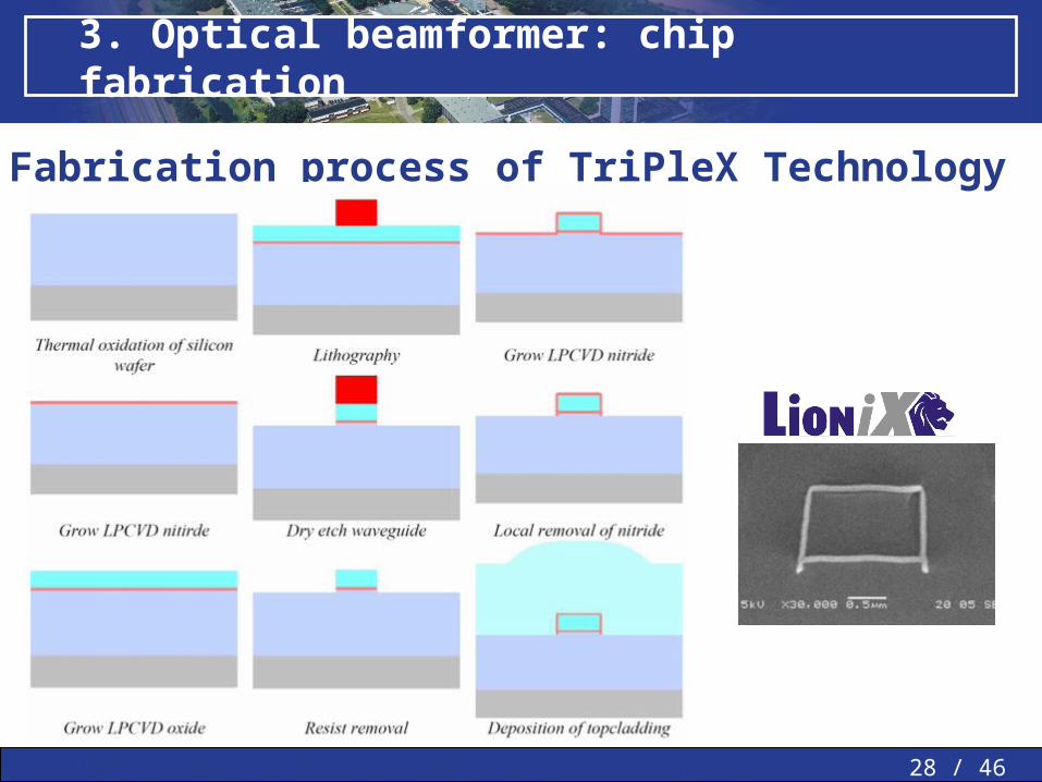
3. Optical beamformer: chip fabrication
Fabrication process of TriPleX Technology
29 / 46MWP » MWP in PAAs » SMART » Conclusions » Questions »
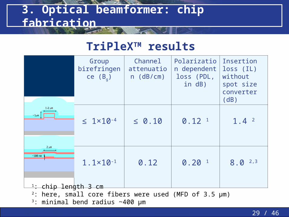
3. Optical beamformer: chip fabrication
TriPleXTM resultsGroup
birefringence (Bg)
Channel attenuation
(dB/cm)
Polarization dependent
loss (PDL, in dB)
Insertion loss (IL) without spot size converter (dB)
≤ 1×10⁻⁴ ≤ 0.10 0.12 1 1.4 2
1.1×10⁻¹
0.12 0.20 1 8.0 2,3
1: chip length 3 cm2: here, small core fibers were used (MFD of 3.5 µm)3: minimal bend radius ~400 µm
1-2 m
~1m
2 m
~100 nm
30 / 46MWP » MWP in PAAs » SMART » Conclusions » Questions »
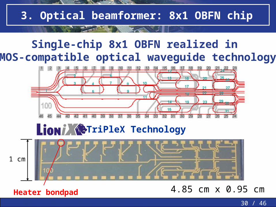
3. Optical beamformer: 8x1 OBFN chip
4.85 cm x 0.95 cm
1 cm
Heater bondpad
TriPleX Technology
Single-chip 8x1 OBFN realized inCMOS-compatible optical waveguide technology
31 / 46MWP » MWP in PAAs » SMART » Conclusions » Questions »
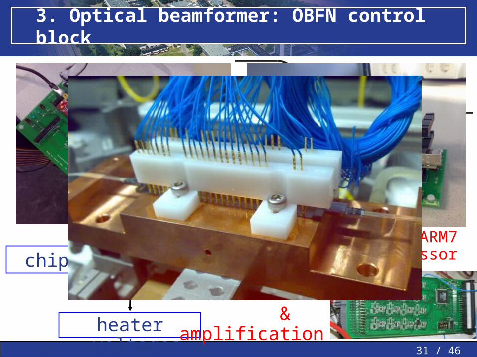
3. Optical beamformer: OBFN control block
beam angle
delays + amplitudes
chip parameters (is and is)
heater voltages
DA conversion & amplification
ARM7microprocessor
436
43
43
1
1
1
2
2
2
5
7
32 / 46MWP » MWP in PAAs » SMART » Conclusions » Questions »
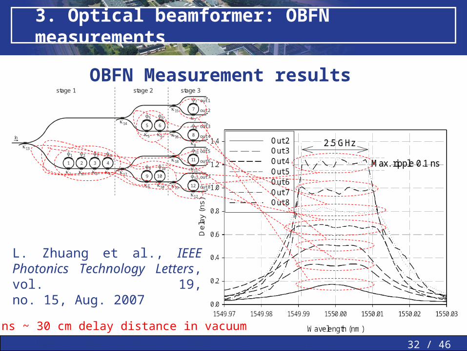
3. Optical beamformer: OBFN measurements
OBFN Measurement results
1 ns ~ 30 cm delay distance in vacuum
5 6 16
5 6
5 6
7
7
out 27
8
8
8
15
out 1
out 4
out 314
9 10 19
9 10
9 10
11
11
out 611
12
12
12
18
out 5
out 8
out 7173 4
3 4
3 4
1 2
1 2
1 2
in
13
stage 1 stage 2 stage 3
L. Zhuang et al., IEEE Photonics Technology Letters, vol. 19,no. 15, Aug. 2007
33 / 46MWP » MWP in PAAs » SMART » Conclusions » Questions »
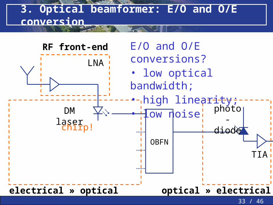
3. Optical beamformer: E/O and O/E conversion
OBFN
electrical » optical optical » electrical
RF front-end
LNA
TIA
DM laser
chirp!
E/O and O/E conversions?• low optical bandwidth;• high linearity;• low noise
photo-diode
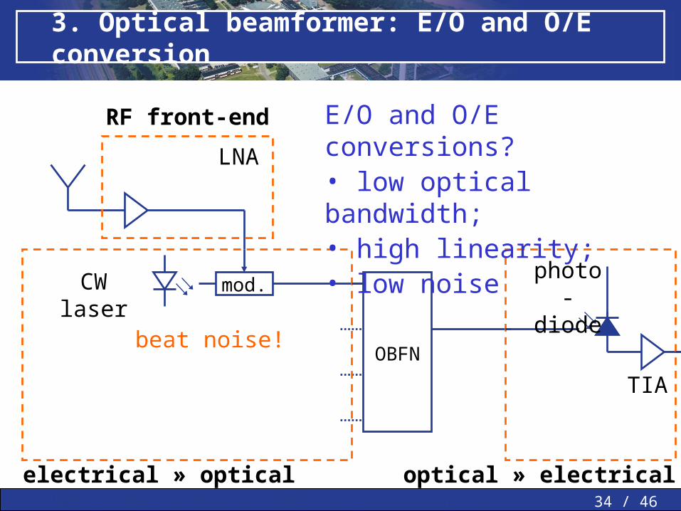
34 / 46MWP » MWP in PAAs » SMART » Conclusions » Questions »
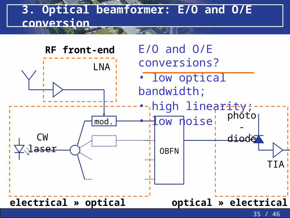
3. Optical beamformer: E/O and O/E conversion
OBFN
electrical » optical optical » electrical
RF front-end
LNA
TIA
CW laser
beat noise!
mod.
E/O and O/E conversions?• low optical bandwidth;• high linearity;• low noise
photo-diode
35 / 46MWP » MWP in PAAs » SMART » Conclusions » Questions »
3. Optical beamformer: E/O and O/E conversion
OBFN
electrical » optical optical » electrical
RF front-end
LNA
TIA
mod.
CW laser
E/O and O/E conversions?• low optical bandwidth;• high linearity;• low noise
photo-diode
36 / 46MWP » MWP in PAAs » SMART » Conclusions » Questions »
3. Optical beamformer: E/O and O/E conversion
mod.
OBFN
RF front-end
LNA
spectrum
frequency
TIA
electrical » optical optical » electrical
CW laser
10.7 GHz
12.75 GHz2 x 12.75 = 25.5 GHz
photo-diode
37 / 46MWP » MWP in PAAs » SMART » Conclusions » Questions »
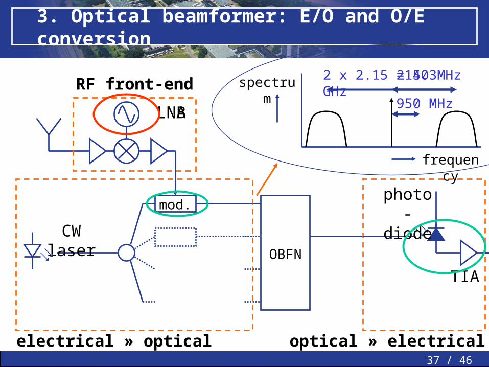
3. Optical beamformer: E/O and O/E conversion
mod.
OBFN
RF front-end
LNALNB
spectrum
frequency
TIA
electrical » optical optical » electrical
CW laser
2 x 2.15 = 4.3 GHz
950 MHz
2150 MHz
photo-diode
38 / 46MWP » MWP in PAAs » SMART » Conclusions » Questions »
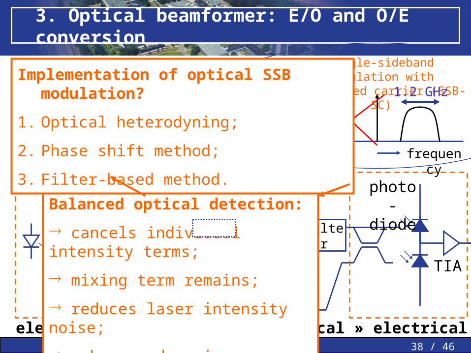
3. Optical beamformer: E/O and O/E conversion
mod.
OBFN
RF front-end
filter
filter
LNB
spectrum
frequency
TIA
single-sideband modulation withsuppressed carrier (SSB-SC)
electrical » optical optical » electrical
CW laser
1.2 GHz
SSB-SCBalanced optical detection:
cancels individual intensity terms;
mixing term remains;
reduces laser intensity noise;
enhances dynamic range.
Implementation of optical SSB modulation?
1. Optical heterodyning;
2. Phase shift method;
3. Filter-based method.
photo-diode
39 / 46MWP » MWP in PAAs » SMART » Conclusions » Questions »
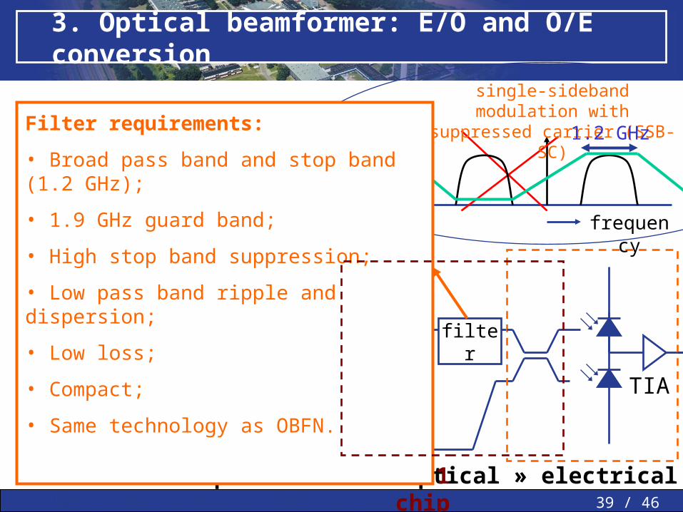
3. Optical beamformer: E/O and O/E conversion
mod.
OBFN
RF front-end
filter
LNB
spectrum
frequency
TIA
single-sideband modulation withsuppressed carrier (SSB-SC)
electrical » optical optical » electrical
CW laser
1.2 GHzFilter requirements:
• Broad pass band and stop band (1.2 GHz);
• 1.9 GHz guard band;
• High stop band suppression;
• Low pass band ripple and dispersion;
• Low loss;
• Compact;
• Same technology as OBFN.
1 chip !
40 / 46MWP » MWP in PAAs » SMART » Conclusions » Questions »
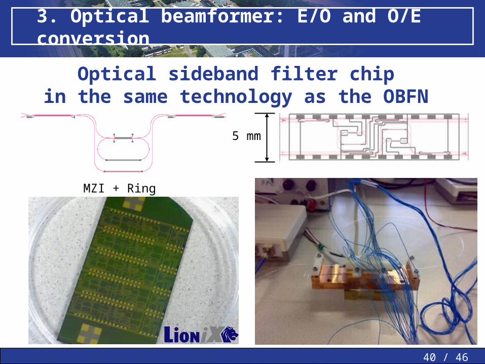
3. Optical beamformer: E/O and O/E conversion
MZI + Ring
5 mm
Optical sideband filter chip in the same technology as the OBFN
41 / 46MWP » MWP in PAAs » SMART » Conclusions » Questions »
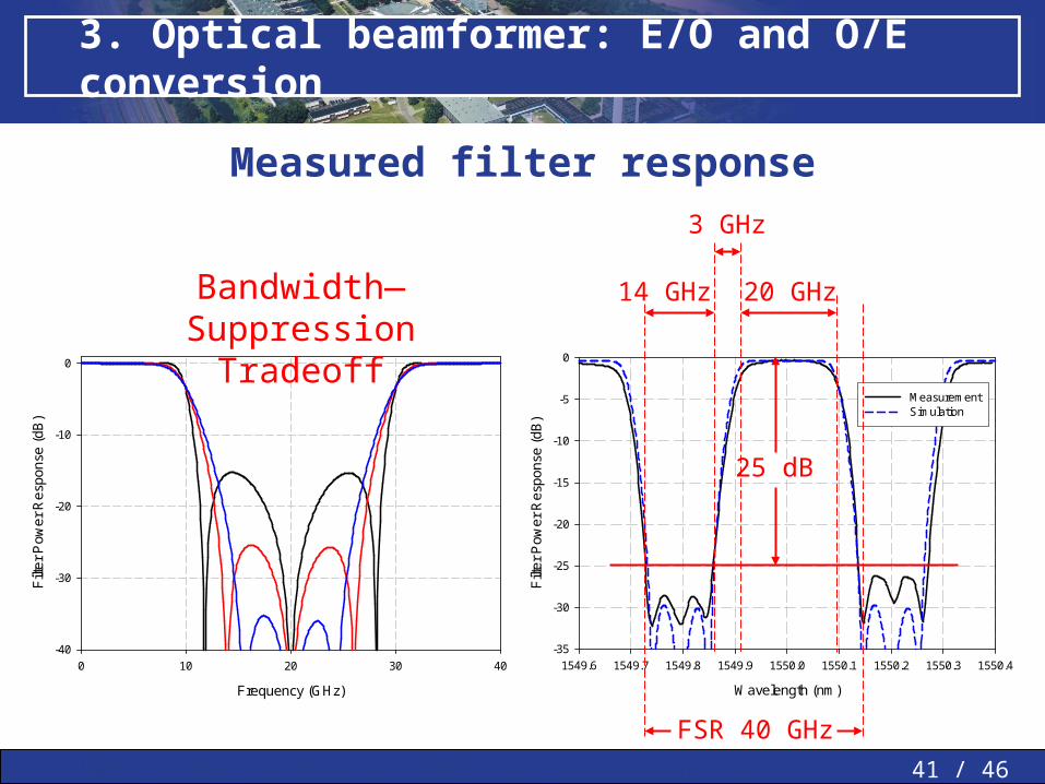
3. Optical beamformer: E/O and O/E conversion
Measured filter response
Wavelength (nm)
1549.6 1549.7 1549.8 1549.9 1550.0 1550.1 1550.2 1550.3 1550.4
Filt
er P
ower
Res
pons
e (d
B)
-35
-30
-25
-20
-15
-10
-5
0
MeasurementSimulation
20 GHz14 GHz
3 GHz
Frequency (GHz)
0 10 20 30 40
Filt
er
Po
we
r R
esp
on
se (
dB
)
-40
-30
-20
-10
0
Bandwidth—Suppression Tradeoff
25 dB
FSR 40 GHz
42 / 46MWP » MWP in PAAs » SMART » Conclusions » Questions »
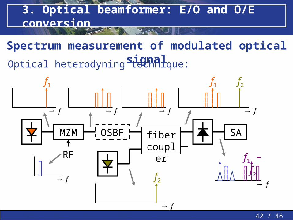
3. Optical beamformer: E/O and O/E conversion
Spectrum measurement of modulated optical signal
Optical heterodyning technique:
f
f f f
f1
f
f1 f2
MZM OSBF SAfiber coupler
RF
f
f1 – f2
f
f2
43 / 46MWP » MWP in PAAs » SMART » Conclusions » Questions »
3. Optical beamformer: E/O and O/E conversion
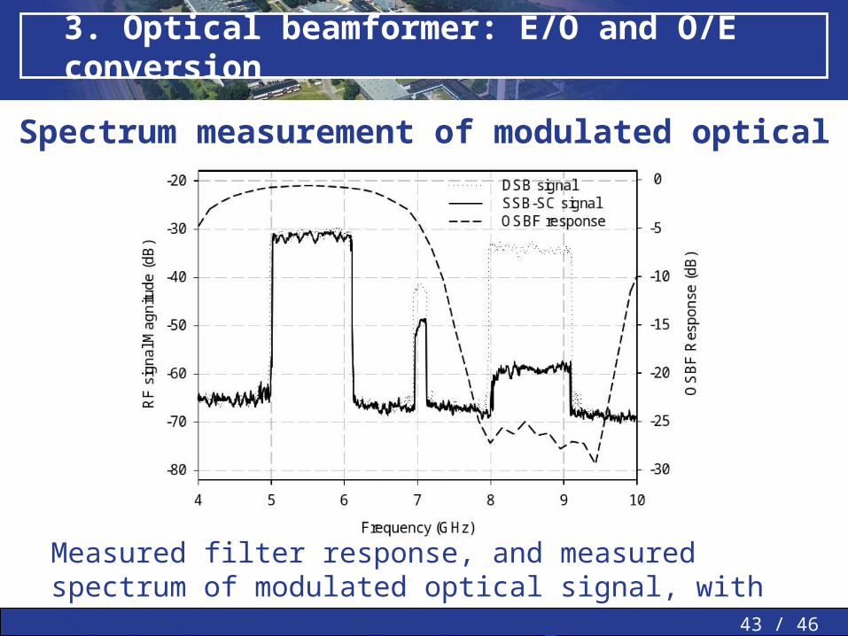
Spectrum measurement of modulated optical signal
Measured filter response, and measured spectrum of modulated optical signal, with and without sideband-filtering
44 / 46MWP » MWP in PAAs » SMART » Conclusions » Questions »
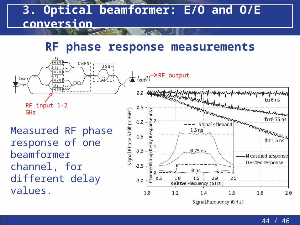
3. Optical beamformer: E/O and O/E conversion
RF phase response measurementsMZM
MZM
I tout( )MZM
MZM
OBFNOSBF
s1( )t
s3( )t
s2( )t
s4( )t
laser
RF input 1-2 GHz
RF output
Measured RF phase response of one beamformer channel, for different delay values.
45 / 46MWP » MWP in PAAs » SMART » Conclusions » Questions »
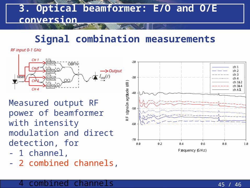
3. Optical beamformer: E/O and O/E conversion
Signal combination measurements
Frequency (GHz)
0.0 0.2 0.4 0.6 0.8 1.0
RF
sig
nal m
agtit
ude
(dB
)
-70
-60
-50
-40
-30
-20
ch 1ch 2ch 3ch 4ch 1&2ch 3&4ch All
CH 1
CH 2
CH 3
CH 4
Output
RF input 0-1 GHz
Measured output RF power of beamformer with intensity modulation and direct detection, for - 1 channel, - 2 combined channels, - 4 combined channels
46 / 46MWP » MWP in PAAs » SMART » Conclusions » Questions »
3. Optical beamformer: Conclusions
Conclusions• A novel squint-free, continuously tunable beamformer mechanism for a phased
array antenna system has been described and partly demonstrated. It is based
on filter-based optical SSB-SC modulation, and ORR-based OBFN, and
balanced coherent detection.
• This scheme minimizes the bandwidth requirements on OBFN and enhances
the dynamic range.
• Different measurements on optical beamformer chip successfully verify the
feasibility of the proposed system.