integral cycle speed control of single phase induction motor using at89c51 microcontroller.pdf
TRANSCRIPT
1
INTEGRAL CYCLE SPEED CONTROL OF SINGLE
PHASE INDUCTION MOTOR USING AT89C51
MICROCONTROLLER AA PPrroojjeecctt RReeppoorrtt SSuubbmmiitttteedd ttoo
JJaawwaahhaarrllaall NNeehhrruu TTeecchhnnoollooggiiccaall UUnniivveerrssiittyy,, HHyyddeerraabbaadd
iinn ppaarrttiiaall ffuullffiillllmmeenntt ffoorr tthhee aawwaarrdd ooff tthhee ddeeggrreeee
BBAACCHHEELLOORR OOFF TTEECCHHNNOOLLOOGGYY
IINN
EELLEECCTTRRIICCAALL AANNDD EELLEECCTTRROONNIICC EENNGGIINNEEEERRIINNGG
Submitted bbyy
BB..SSAASSHHIIDDAARR RREEDDDDYY 0099224455AA00221122
MM..SSUUBBHHAASSHH 0088224411AA00224488
PP..RRUUPPAAKK PPRRAANNAAVV TTEEJJ 0088224411AA00224411
MM..AABBHHIISSHHEEKK 0088224411AA00220022
Under the Guidance of
K.SATISH KUMAR, Asst. Professor
DEPARTMENT OF ELECTRICAL AND ELECTRONIC ENGINEERING
GOKARAJU RANGARAJU COLLEGE OF ENGINEERING AND
TECHNOLOGY
HYDERABAD, ANDHRA PRADESH

2
CCEERRTTIIFFIICCAATTEE
This is to certify that this project report entitled “INTEGRAL CYCLE 1PHASE
INDUCTION MOTOR SPEED CONTROL USING MICRO CONTROLLER” that is
being submitted by B.SASHIDAR REDDY, M.SUBHASH, P.RUPAK PRANAV TEJ, M.
ABHISHEK, in partial fulfillment for the award of the degree of Bachelor of Technology in
ELECTRICAL AND ELECTRONIC ENGINEERING to the Jawaharlal Nehru
Technological University is a record of bonafide work carried out by him under my guidance
and supervision. The results embodied in this project report have not been submitted to any
other University or Institute for the award of any degree or diploma.
HEAD OF THE DEPARTMENT INTERNAL GUIDE
MR.P.M.SARMA K.SATISH KUMAR EEE DPT EEE DPT
GRIET, HYDERABAD

3
ACKNOWLEDEGEMENT
I thank Sri. P. S. Raju Garu, Prof.EEE and Director of Gokaraju Rangaraju Institute of
Engineering And Technology, Hyderabad for the facilities provided and constant
encouragement.
I take our pleasure to acknowledge Dr. J.N.M Murthy Garu, Principal of Gokaraju
Rangaraju Institute Of Engineering And Technology, Hyderabad, for providing good environment for studies and continuous support in achieving our goals.
We are also thankful to Dr. S. N. Saxena, Prof. EEE for providing us constant guidance and
giving us regular feedback on the work done by us, which helped us a great deal to complete our project in time and with desired outputs.
I would like to express gratitude and indebtedness to MR.P.M. Sharma, HOD.EEE and
Sri. M. Chakravarthy, Prof. EEE, for their valuable advice and guidance without which this
project would not have seen the light of the day.
I would also thank MR.K SATISH KUMAR, Asst. Prof.EEE for his guidance and support
due to which the project has been a success.
The satisfaction and euphoria that accompany the successful completion of the task would be
great, but incomplete without the mention of the people who made it possible, whose constant
guidance and encouragement crown all the efforts with success. In this context, I would like
to thank all the other staff members, both teaching and non-teaching, who have extended their
timely help and eased my task.
ABSTRACT
Now a days speed control of single phase induction motor has got more importance and used
in many applications. We are using various methods to control the speed. This project is
basically designed to control the 1-phase induction motor speed Effectively and
economically.
Integral cycle control is a method to remove portions of full cycles/one cycle of an ac signal
for controlling ac power across fan loads interfaced to a programmed micro controller. In
Integral cycle control supply is switched on to the load for some cycles called ON cycles and
supply is switched off to the load for some cycles called OFF cycles by varying this ON and
OFF cycles we can get variable voltage across the load i.e fan. Hence we can get variable

4
controlled speed .This process of power control generates 1% total harmonic distortion as
against 61% of phase angle control. There by harmonic losses are less, hence having more
efficiency.
This type of control is used in applications which have high mechanical inertia and high
thermal time constant (such as industrial heating and speed control of ac motors).
CONTENTS
Chapters Page. No
1. Introduction
1.1 AC Voltage Controllers 1-8 1.1.1 Phase Control 1.1.2 Integral Cycle Control
1.2 Principle of Integral Cycle Control 9-16 1.2.1 Circuit Diagram/Block Diagram 1.2.2 Theory 1.2.3 Output Voltage Waveforms 1.2.4 Derivations of R.M.S Voltage, Current and PF
1.3 Micro Controller 8051 17
1.3.1 Block Diagram 1.3.2 Pin Diagram/Pin Description
1.3.3 Registers
1.3.4 Timers and Interrupts
1.4 Optocoupler 21 1.4.1 Theory 1.4.2 Circuit Diagrams
1.4.3 Symbols and Abberiviations
1.5 Triac 23 1.5.1 Name of Device and Symbol
1.5.2 Latch and Hold Characteristics 1.5.3 Characteristics of the Triac
1.5.4 Methods of Control AC Switch 1.5.5 Zero Point Switching 1.5.6 Zero Point Switching Techniques
5
1.6 Single Phase Induction Motor 28 1.6.1 Theory
1.6.2 Motor Slip 1.6.3 Equivalent Circuit
1.7Push Buttons 31 1.7.1 images
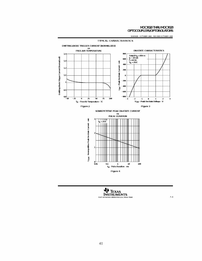
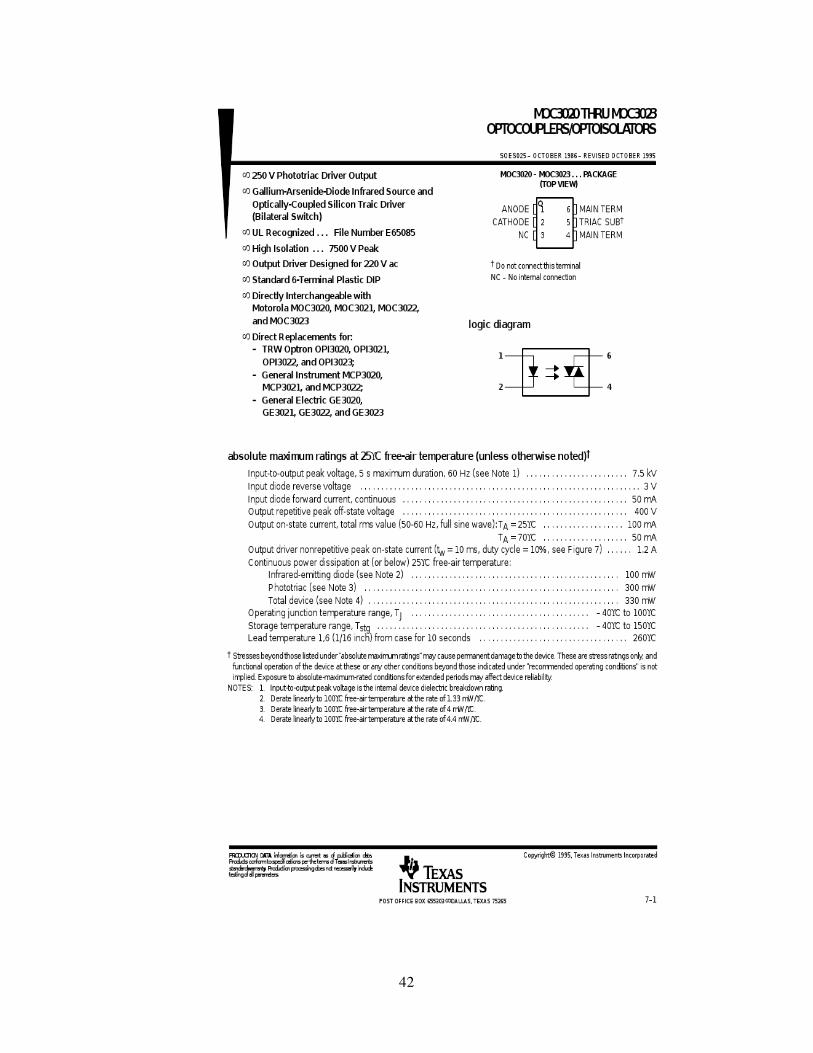
1.8. Data Sheets 32 1.8.1 Micro controller 8051 (AT89S52) 1.8.2 Optocoupler MOC3021
1.8.3 Triac BTA12
LIST OF FIGURES PAGE
NO
FIG 1.1 AC TO VARIABLE AC 6
FIG 1.2 SINGLE PHASE FULL WAVE AC VOLTAGE CONTROLLER 9
FIG 1.3 WAVEFORMS 12
FIG 1.4 BLOCK DIAGRAM OF MICRO CONTROLLER 8051 16
FIG 1.5 40-LEAD PDIP 17
FIG 1.6 IMAGES OF OPTOCOUPLER 21
FIG 1.7 TRIAC 23
FIG 1.8 TRIAC VPLTAGE CHARACTERISTICS 24
FIG 1.9 EQUIVALENT CIRCUIT OF MOTOR 29
FIG 2.1 SCHEMATIC DIAGRAM 30
CHAPTER1
Introduction
AC VOLTAGE CONTROLLER (AC-AC CONVERTER)
AC voltage controllers (ac line voltage controllers) are employed to vary the RMS value of the
alternating voltage applied to a load circuit by introducing thyristors between the load and a
constant voltage ac source. The RMS value of alternating voltage applied to load circuit is controlled by controlling the triggering angle of the thyristors in the ac voltage controller
circuits. In brief, an ac voltage controller is a type of thyristor power converter which is used to
convert a fixed voltage, fixed frequency ac input supply to obtain a variable voltage ac output.
6
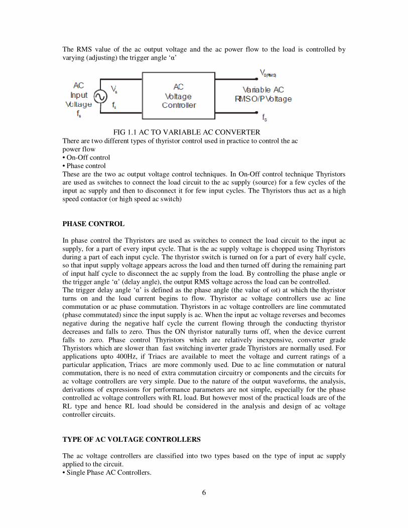
The RMS value of the ac output voltage and the ac power flow to the load is controlled by
varying (adjusting) the trigger angle ‘α’
FIG 1.1 AC TO VARIABLE AC CONVERTER There are two different types of thyristor control used in practice to control the ac
power flow
• On-Off control
• Phase control
These are the two ac output voltage control techniques. In On-Off control technique Thyristors are used as switches to connect the load circuit to the ac supply (source) for a few cycles of the
input ac supply and then to disconnect it for few input cycles. The Thyristors thus act as a high
speed contactor (or high speed ac switch)
PHASE CONTROL
In phase control the Thyristors are used as switches to connect the load circuit to the input ac
supply, for a part of every input cycle. That is the ac supply voltage is chopped using Thyristors
during a part of each input cycle. The thyristor switch is turned on for a part of every half cycle, so that input supply voltage appears across the load and then turned off during the remaining part
of input half cycle to disconnect the ac supply from the load. By controlling the phase angle or
the trigger angle ‘α’ (delay angle), the output RMS voltage across the load can be controlled. The trigger delay angle ‘α’ is defined as the phase angle (the value of ωt) at which the thyristor
turns on and the load current begins to flow. Thyristor ac voltage controllers use ac line
commutation or ac phase commutation. Thyristors in ac voltage controllers are line commutated (phase commutated) since the input supply is ac. When the input ac voltage reverses and becomes
negative during the negative half cycle the current flowing through the conducting thyristor
decreases and falls to zero. Thus the ON thyristor naturally turns off, when the device current
falls to zero. Phase control Thyristors which are relatively inexpensive, converter grade Thyristors which are slower than fast switching inverter grade Thyristors are normally used. For
applications upto 400Hz, if Triacs are available to meet the voltage and current ratings of a
particular application, Triacs are more commonly used. Due to ac line commutation or natural commutation, there is no need of extra commutation circuitry or components and the circuits for
ac voltage controllers are very simple. Due to the nature of the output waveforms, the analysis,
derivations of expressions for performance parameters are not simple, especially for the phase controlled ac voltage controllers with RL load. But however most of the practical loads are of the
RL type and hence RL load should be considered in the analysis and design of ac voltage
controller circuits.
TYPE OF AC VOLTAGE CONTROLLERS
The ac voltage controllers are classified into two types based on the type of input ac supply
applied to the circuit.
• Single Phase AC Controllers.

7
• Three Phase AC Controllers.
Single phase ac controllers operate with single phase ac supply voltage of 230V RMS at 50Hz in
our country. Three phase ac controllers operate with 3 phase ac supply of 400V RMS at 50Hz supply frequency.
Each type of controller may be sub divided into
• Uni-directional or half wave ac controller.
• Bi-directional or full wave ac controller. In brief different types of ac voltage controllers are
• Single phase half wave ac voltage controller (uni-directional controller).
• Single phase full wave ac voltage controller (bi-directional controller). • Three phase half wave ac voltage controller (uni-directional controller).
• Three phase full wave ac voltage controller (bi-directional controller).
APPLICATIONS OF AC VOLTAGE CONTROLLERS
• Lighting / Illumination control in ac power circuits.
• Induction heating.
• Industrial heating & Domestic heating.
• Transformer tap changing (on load transformer tap changing). • Speed control of induction motors (single phase and poly phase ac induction motor control).
• AC magnet controls.

8
PRINCIPLE OF ON-OFF CONTROL TECHNIQUE (INTEGRAL CYCLE CONTROL)
The basic principle of on-off control technique is explained with reference to a single phase full
wave ac voltage controller circuit shown below. The thyristor switches 1 T and 2 T are turned on by applying appropriate gate trigger pulses to connect the input ac supply to the load for ‘n’
number of input cycles during the time interval ON t . The 3 thyristor switches 1 T and 2 T are turned
off by blocking the gate trigger pulses for ‘m’ number of input cycles during the time interval OFF t
The ac controller ON time t usually consists of an integral number of input cycles.

9

10
Thyristors are turned ON precisely at the zero voltage crossings of the input supply.The
thyristor 1 T is turned on at the beginning of each positive half cycle by applying the gate trigger
pulses to 1 T as shown, during the ON time ON t . The load current flows in the positive direction, which is the downward direction as shown in the circuit diagram when 1 T conducts. The thyristor
2 T is turned on at the beginning of each negative half cycle, by applying gating signal to the gate
of 2 T , during ON t . The load current flows in the reverse direction, which is the upward direction
when 2 T conducts. Thus we obtain a bi-directional load current flow (alternating load current flow) in a ac voltage controller circuit, by triggering the thyristors alternately.
This type of control is used in applications which have high mechanical inertia and high thermal
time constant (Industrial heating and speed control of ac motors). Due to zero voltage and zero current switching of Thyristors, the harmonics generated by switching actions are reduced.
For a sine wave input supply voltage, vs =Vm sinωt = 2VS sinωtS V =RMS value of input ac supply
=2m V = RMS phase supply voltage. If the input ac supply is connected to load for ‘n’ number of input cycles and disconnected for ‘m’ number of input cycles, then, ON OFF t = n×T t =m×T Where
T 1f= = input cycle time (time period) andf = input supply frequency.
ON t = controller on time = n×T . OFF t = controller off time = m×T .
O T = Output time period = ( ) ( ) ON OFF t + t = nT + mT .

11

12

13
14
15
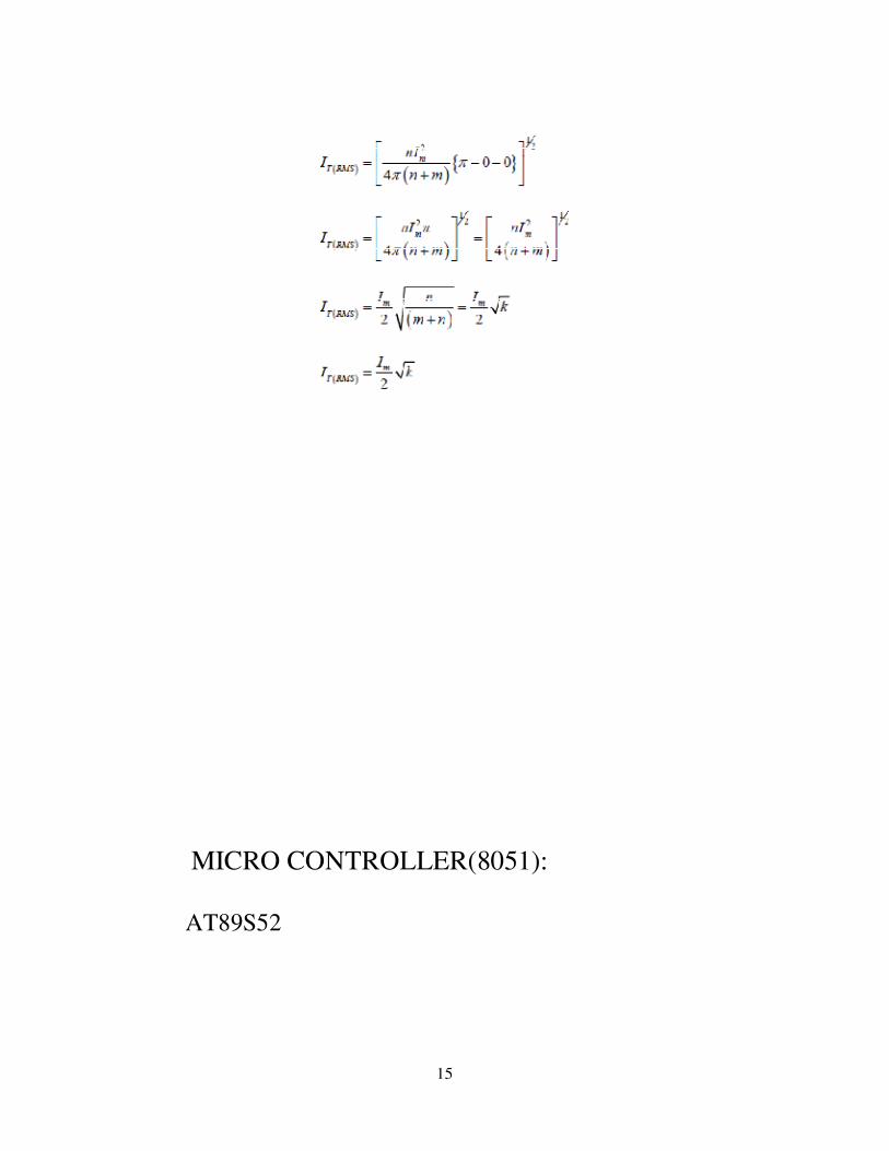
MICRO CONTROLLER(8051):
AT89S52

16
FIG 1.4 BLOCK DIAGRAM OF 8051
4. Pin Description
4.1 VCC Supply voltage.
4.2 GND Ground.
4.3 Port 0
Port 0 is an 8-bit open drain bidirectional I/O port. As an output port, each pin can sink eight TTL inputs. When 1s are written to port 0 pins, the pins can be used as high-
impedance inputs. Port 0 can also be configured to be the multiplexed low-order address/data bus during accesses to external program and data memory. In this mode, Phase internal pull-
ups. Port 0 also receives the code bytes during Flash programming and outputs the code bytes dur-ing program verification. External pull-ups are required during program verification.

17
FIG 1.5 40-LEAD PDIP
4.4 Port 1 Port 1 is an 8-bit bidirectional I/O port with internal pull-ups. The Port 1
output buffers can sink/source four TTL inputs. When 1s are written to Port 1 pins, they are
pulled high by the inter-nal pull-ups and can be used as inputs. As inputs, Port 1 pins that are
externally being pulled low will source current (IIL) because of the internal pull-ups. In
addition, P1.0 and P1.1 can be configured to be the timer/counter 2 external count input
(P1.0/T2) and the timer/counter 2 trigger input (P1.1/T2EX), respectively, as shown in the
follow-ing table. Port 1 also receives the low-order address bytes during Flash programming
and verification.
Port Pin Alternate Functions
P1.0 T2 (external count input to Timer/Counter 2), clock-out
P1.1 T2EX (Timer/Counter 2 capture/reload trigger and direction control P1.5 MOSI (used for In-System Programming)
P1.6 MISO (used for In-System Programming)
P1.7 SCK (used for In-System Programming)
4.5 Port 2 Port 2 is an 8-bit bidirectional I/O port with internal pull-ups. The Port 2
output buffers can sink/source four TTL inputs. When 1s are written to Port 2 pins, they are
pulled high by the inter-nal pull-ups and can be used as inputs. As inputs, Port 2 pins that are
externally being pulled low will source current (IIL) because of the internal pull-ups. Port 2
emits the high-order address byte during fetches from external program memory and dur-ing
accesses to external data memory that use 16-bit addresses (MOVX @ DPTR). In this
application, Port 2 uses strong internal pull-ups when emitting 1s. During accesses to external
data memory that use 8-bit addresses (MOVX @ RI), Port 2 emits the contents of the P2

18
Special Function Register. Port 2 also receives the high-order address bits and some control
signals during Flash program-ming and verification.
Port 3 Port 3 is an 8-bit bidirectional I/O port with internal pull-ups. The Port 3
output buffers can sink/source four TTL inputs. When 1s are written to Port 3 pins, they are
pulled high by the inter-nal pull-ups and can be used as inputs. As inputs, Port 3 pins that are externally being pulled low will source current (IIL) because of the pull-ups. Port 3 receives
some control signals for Flash programming and verification. Port 3 also serves the functions of various special features of the AT89S52, as shown in the fol-lowing table.
Port Pin Alternate Functions P3.0 RXD (serial input port)
P3.1 TXD (serial output port)
P3.2 INT0 (external interrupt 0)
P3.3 INT1 (external interrupt 1)
P3.4 T0 (timer 0 external input)
P3.5 T1 (timer 1 external input)
P3.6 WR (external data memory write strobe) P3.7 RD (external data memory read
strobe)
5 1919D–MICRO–6/08 AT89S52
4.6 Port 3 Port 3 is an 8-bit bidirectional I/O port with internal pull-ups. The Port 3
output buffers can sink/source four TTL inputs. When 1s are written to Port 3 pins, they are
pulled high by the inter-nal pull-ups and can be used as inputs. As inputs, Port 3 pins that are
externally being pulled low will source current (IIL) because of the pull-ups. Port 3 receives
some control signals for Flash programming and verification. Port 3 also serves the functions of various special features of the AT89S52, as shown in the fol-lowing table.
4.7 RST Reset input. A high on this pin for two machine cycles while the oscillator is running resets the device. This pin drives high for 98 oscillator periods after the Watchdog
times out. The DISRTO bit in SFR AUXR (address 8EH) can be used to disable this feature. In the default state of bit DISRTO, the RESET HIGH out feature is enabled.
4.8 ALE/PROG Address Latch Enable (ALE) is an output pulse for latching the low byte of the address during accesses to external memory. This pin is also the program pulse
input (PROG) during Flash programming. In normal operation, ALE is emitted at a constant
rate of 1/6 the oscillator frequency and may be used for external timing or clocking purposes.
Note, however, that one ALE pulse is skipped dur-ing each access to external data memory.
If desired, ALE operation can be disabled by setting bit 0 of SFR location 8EH. With the bit
set, ALE is active only during a MOVX or MOVC instruction. Otherwise, the pin is weakly
pulled high. Setting the ALE-disable bit has no effect if the microcontroller is in external
execution mode.
9 PSEN Program Store Enable (PSEN) is the read strobe to external program
memory. When the AT89S52 is executing code from external program memory, PSEN is
activated twice each machine cycle, except that two PSEN activations are skipped during
each access to exter-nal data memory.
4.10 EA/VPP External Access Enable. EA must be strapped to GND in order to enable the device to fetch code from external program memory locations starting at 0000H up
to FFFFH. Note, however, that if lock bit 1 is programmed, EA will be internally latched on reset. EA should be strapped to VCC for internal program executions. This pin also receives
the 12-volt programming enable voltage (VPP) during Flash programming.
19
4.11 XTAL1 Input to the inverting oscillator amplifier and input to the internal clock
operating circuit. 4.12 XTAL2 Output from the inverting oscillator amplifier.
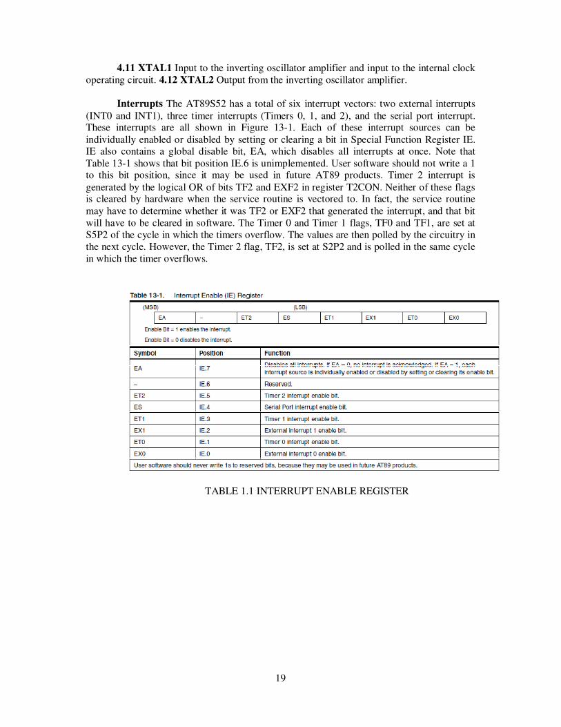
Interrupts The AT89S52 has a total of six interrupt vectors: two external interrupts
(INT0 and INT1), three timer interrupts (Timers 0, 1, and 2), and the serial port interrupt. These interrupts are all shown in Figure 13-1. Each of these interrupt sources can be
individually enabled or disabled by setting or clearing a bit in Special Function Register IE. IE also contains a global disable bit, EA, which disables all interrupts at once. Note that
Table 13-1 shows that bit position IE.6 is unimplemented. User software should not write a 1 to this bit position, since it may be used in future AT89 products. Timer 2 interrupt is
generated by the logical OR of bits TF2 and EXF2 in register T2CON. Neither of these flags is cleared by hardware when the service routine is vectored to. In fact, the service routine
may have to determine whether it was TF2 or EXF2 that generated the interrupt, and that bit
will have to be cleared in software. The Timer 0 and Timer 1 flags, TF0 and TF1, are set at
S5P2 of the cycle in which the timers overflow. The values are then polled by the circuitry in
the next cycle. However, the Timer 2 flag, TF2, is set at S2P2 and is polled in the same cycle
in which the timer overflows.
TABLE 1.1 INTERRUPT ENABLE REGISTER
20
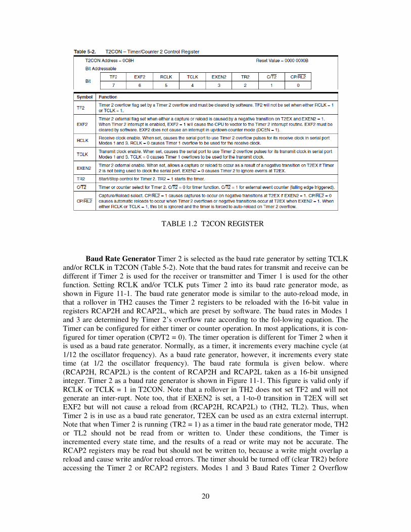
TABLE 1.2 T2CON REGISTER
Baud Rate Generator Timer 2 is selected as the baud rate generator by setting TCLK
and/or RCLK in T2CON (Table 5-2). Note that the baud rates for transmit and receive can be
different if Timer 2 is used for the receiver or transmitter and Timer 1 is used for the other
function. Setting RCLK and/or TCLK puts Timer 2 into its baud rate generator mode, as
shown in Figure 11-1. The baud rate generator mode is similar to the auto-reload mode, in
that a rollover in TH2 causes the Timer 2 registers to be reloaded with the 16-bit value in
registers RCAP2H and RCAP2L, which are preset by software. The baud rates in Modes 1
and 3 are determined by Timer 2’s overflow rate according to the fol-lowing equation. The
Timer can be configured for either timer or counter operation. In most applications, it is con-
figured for timer operation (CP/T2 = 0). The timer operation is different for Timer 2 when it is used as a baud rate generator. Normally, as a timer, it increments every machine cycle (at
1/12 the oscillator frequency). As a baud rate generator, however, it increments every state time (at 1/2 the oscillator frequency). The baud rate formula is given below. where
(RCAP2H, RCAP2L) is the content of RCAP2H and RCAP2L taken as a 16-bit unsigned integer. Timer 2 as a baud rate generator is shown in Figure 11-1. This figure is valid only if
RCLK or TCLK = 1 in T2CON. Note that a rollover in TH2 does not set TF2 and will not generate an inter-rupt. Note too, that if EXEN2 is set, a 1-to-0 transition in T2EX will set
EXF2 but will not cause a reload from (RCAP2H, RCAP2L) to (TH2, TL2). Thus, when
Timer 2 is in use as a baud rate generator, T2EX can be used as an extra external interrupt.
Note that when Timer 2 is running (TR2 = 1) as a timer in the baud rate generator mode, TH2
or TL2 should not be read from or written to. Under these conditions, the Timer is
incremented every state time, and the results of a read or write may not be accurate. The
RCAP2 registers may be read but should not be written to, because a write might overlap a
reload and cause write and/or reload errors. The timer should be turned off (clear TR2) before
accessing the Timer 2 or RCAP2 registers. Modes 1 and 3 Baud Rates Timer 2 Overflow

21
Rate 16 ----------------------------------------------------------- = Modes 1 and 3 Baud Rate --------
------------------------------- Oscillator Frequency 32 x [65536-RCAP2H,RCAP2L)]
OPTOCOUPLER THEORY:
1. INTRODUCTION
This application note discusses the common mode transient immunity (CMTI) properties of
optocouplers. It covers phototransistor output and optically coupled logic gates. Common mode transient immunity, (CMTI), common mode transient rejection (CMTR), or common
mode rejection(CMR), are a measure of ability of an optocoupler’s output amplifier to reject fast transient noise signals that are present between the input (LED) and the output side of the
optocoupler. To characterize the CMTI behavior of an optocoupler it is necessary to describe it with two values: • VCM - common mode voltage (VCM = VCM)• dV/dt - rate of rise or
fall of the common mode voltage(dV/dt = VCM/tr or dV/dt = VCM/tf)Figure 1 shows
how these two values are defined. Only when both values are specified can the CMTI be
evaluated properly. The ability of the optocoupler to withstand a given common mode
transient is called common mode transient immunity at logic low level or logic high level; the
abbreviation is CML or CMH. The optocoupler fails if its output ’high’ voltage drops below
2.0 V or its output ’low’ voltage rises above 0.8 V, in the presence of the common mode
transient noise signal.
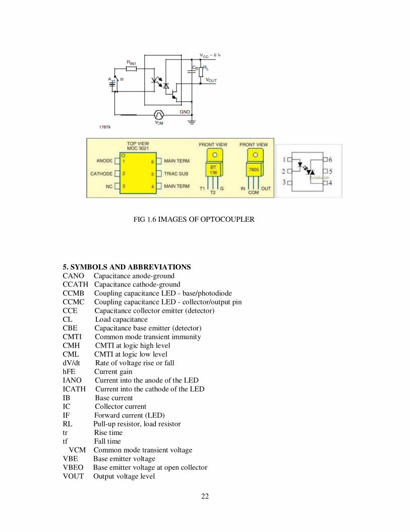
22
FIG 1.6 IMAGES OF OPTOCOUPLER
5. SYMBOLS AND ABBREVIATIONS
CANO Capacitance anode-ground CCATH Capacitance cathode-ground
CCMB Coupling capacitance LED - base/photodiode
CCMC Coupling capacitance LED - collector/output pin
CCE Capacitance collector emitter (detector)
CL Load capacitance
CBE Capacitance base emitter (detector)
CMTI Common mode transient immunity
CMH CMTI at logic high level
CML CMTI at logic low level
dV/dt Rate of voltage rise or fall
hFE Current gain
IANO Current into the anode of the LED
ICATH Current into the cathode of the LED
IB Base current IC Collector current
IF Forward current (LED) RL Pull-up resistor, load resistor
tr Rise time
tf Fall time
VCM Common mode transient voltage
VBE Base emitter voltage
VBEO Base emitter voltage at open collector
VOUT Output voltage level
23
VOH Output voltage at high level
VOL Output voltage at low level
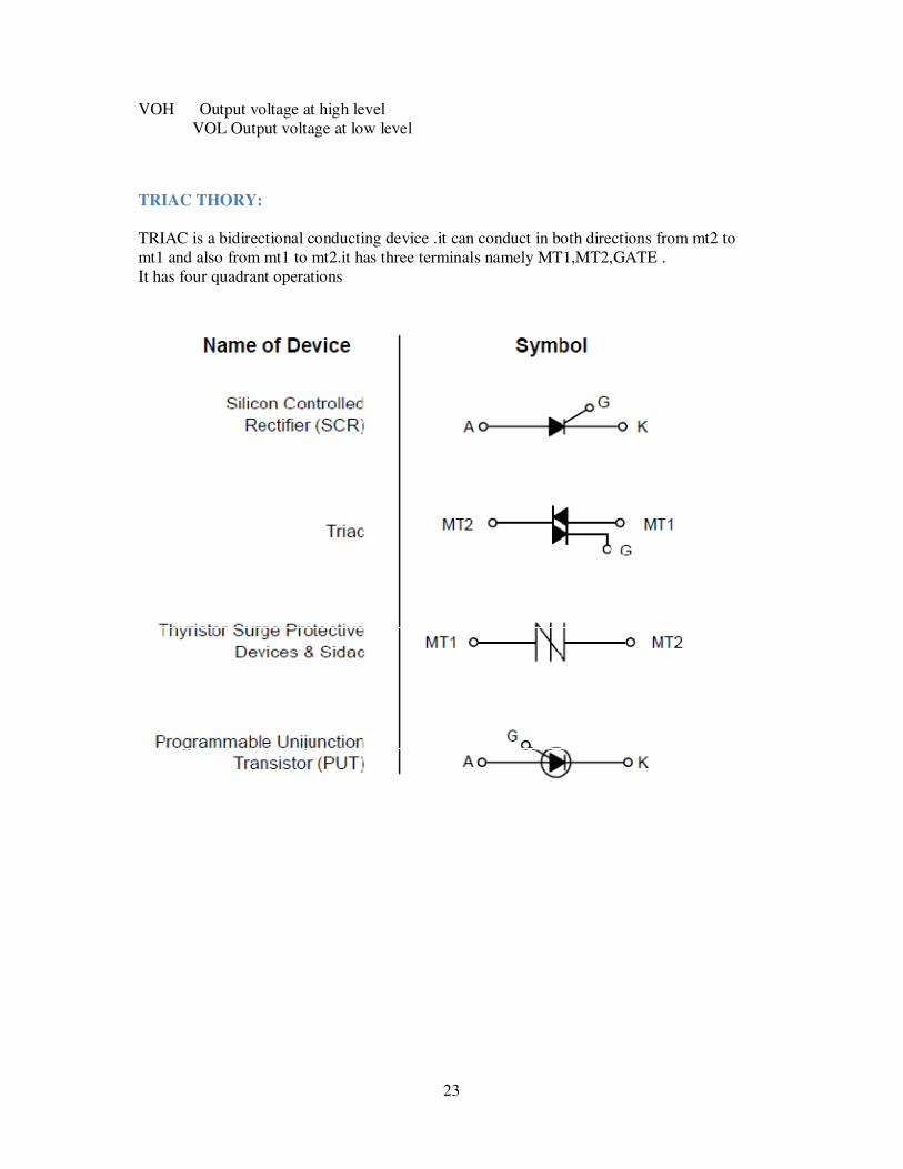
TRIAC THORY:
TRIAC is a bidirectional conducting device .it can conduct in both directions from mt2 to
mt1 and also from mt1 to mt2.it has three terminals namely MT1,MT2,GATE .
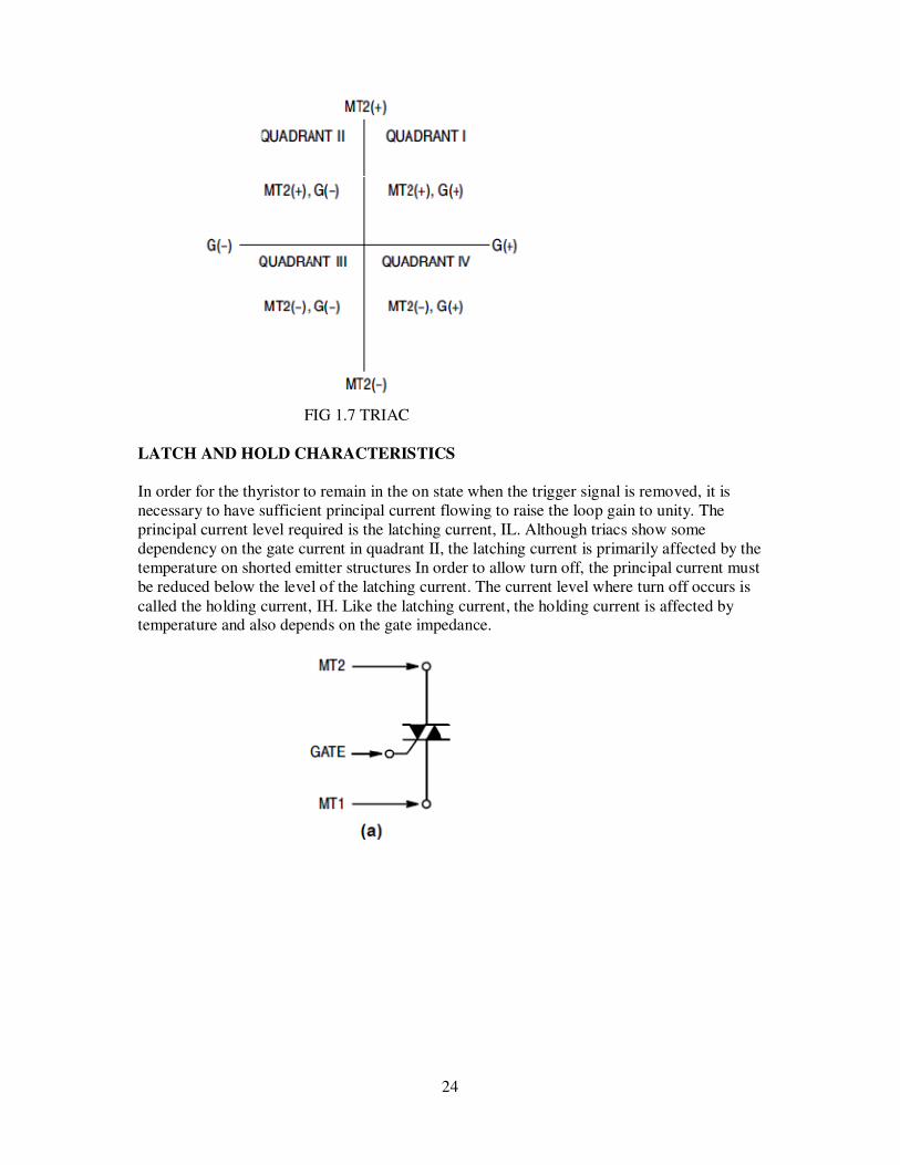
It has four quadrant operations
24
FIG 1.7 TRIAC
LATCH AND HOLD CHARACTERISTICS
In order for the thyristor to remain in the on state when the trigger signal is removed, it is
necessary to have sufficient principal current flowing to raise the loop gain to unity. The
principal current level required is the latching current, IL. Although triacs show some
dependency on the gate current in quadrant II, the latching current is primarily affected by the
temperature on shorted emitter structures In order to allow turn off, the principal current must
be reduced below the level of the latching current. The current level where turn off occurs is
called the holding current, IH. Like the latching current, the holding current is affected by temperature and also depends on the gate impedance.
25
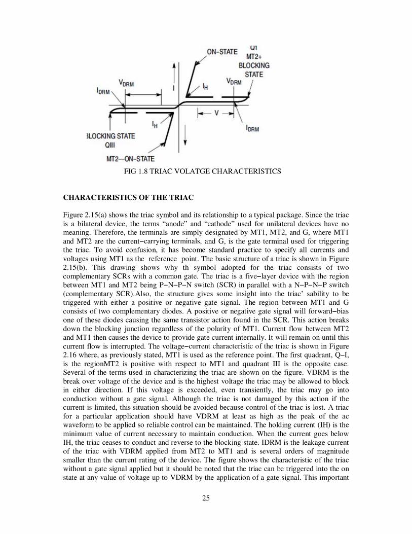
FIG 1.8 TRIAC VOLATGE CHARACTERISTICS
CHARACTERISTICS OF THE TRIAC
Figure 2.15(a) shows the triac symbol and its relationship to a typical package. Since the triac
is a bilateral device, the terms “anode” and “cathode” used for unilateral devices have no meaning. Therefore, the terminals are simply designated by MT1, MT2, and G, where MT1
and MT2 are the current−carrying terminals, and G, is the gate terminal used for triggering the triac. To avoid confusion, it has become standard practice to specify all currents and
voltages using MT1 as the reference point. The basic structure of a triac is shown in Figure
2.15(b). This drawing shows why th symbol adopted for the triac consists of two
complementary SCRs with a common gate. The triac is a five−layer device with the region
between MT1 and MT2 being P−N−P−N switch (SCR) in parallel with a N−P−N−P switch
(complementary SCR).Also, the structure gives some insight into the triac’ sability to be
triggered with either a positive or negative gate signal. The region between MT1 and G
consists of two complementary diodes. A positive or negative gate signal will forward−bias
one of these diodes causing the same transistor action found in the SCR. This action breaks
down the blocking junction regardless of the polarity of MT1. Current flow between MT2
and MT1 then causes the device to provide gate current internally. It will remain on until this
current flow is interrupted. The voltage−current characteristic of the triac is shown in Figure 2.16 where, as previously stated, MT1 is used as the reference point. The first quadrant, Q−I,
is the regionMT2 is positive with respect to MT1 and quadrant III is the opposite case. Several of the terms used in characterizing the triac are shown on the figure. VDRM is the
break over voltage of the device and is the highest voltage the triac may be allowed to block in either direction. If this voltage is exceeded, even transiently, the triac may go into
conduction without a gate signal. Although the triac is not damaged by this action if the current is limited, this situation should be avoided because control of the triac is lost. A triac
for a particular application should have VDRM at least as high as the peak of the ac waveform to be applied so reliable control can be maintained. The holding current (IH) is the
minimum value of current necessary to maintain conduction. When the current goes below
IH, the triac ceases to conduct and reverse to the blocking state. IDRM is the leakage current
of the triac with VDRM applied from MT2 to MT1 and is several orders of magnitude
smaller than the current rating of the device. The figure shows the characteristic of the triac
without a gate signal applied but it should be noted that the triac can be triggered into the on
state at any value of voltage up to VDRM by the application of a gate signal. This important
26
characteristic makes the triac very useful. Since the triac will conduct in either direction and
can be triggered with either a positive or negative gate signal there are four possible
triggering modes (Figure 2.3): Quadrant I; MT2 (+), G(+), positive voltage and positive gate
current. Quadrant II; MT2 (+), G (−), positive voltage and negative gate current. Quadrant
III; MT2 (−), G(−), negative voltage and negative gate current. Quadrant IV; MT2 (−), G(+),
negative voltage and positive gate current. Present triacs are most sensitive in quadrants I and
III, slightly less so in quadrant II, and much less sensitive in quadrant IV. Therefore it is not recommended to use quadrant IV unless special circumstances dictate it. An important fact to
remember is that since a triac can conduct current in both directions, it has only a brief interval during which the sine wave current is passing through zero to recover and revert to
its blocking state. OF or this reason, reliable operation of present triacs is limited to 60 Hz line frequency and lower frequencies. For inductive loads, the phase−shift between the
current and voltage means that at the time the current falls below IH and the triac ceases to
conduct, there exists a certain voltage which must appear across the triac. If this voltage
Appears too rapidly, the triac will resume conduction and control is lost. In order to achieve
control with certain inductive loads, the rate of rise in voltage (dv/dt) must be limited by a
series RC network across the triac. The capacitor will then limit the (dv/dt) across the triac.
The resistor is necessary to limit the surge of current from the capacitor when the triac fires,
and to damp the ringing of the capacitance with the load inductance.
METHODS OF CONTROL AC SWITCH
A useful application of triac is as a direct replacement for an ac mechanical relay. In this application, the triac on−off control and the power−regulating ability of the triac is not
utilized. The control circuitry for this application is usually very simple, consisting of a source for the gate signal and some type of small current switch, either mechanical or
electrical. The gate signal can be obtained from a separate source or directly from the line voltage at terminal MT2 of the triac.
PHASE CONTROL
An effective and widely−used method of controlling the average power to a load through the
triac is by phase control. Phase control is a method of utilizing the triac to apply the ac supply
to the load for a controlled fraction of each cycle. In this mode of operation, the triac is held
in an off or open condition for a portion of each positive and negative cycle, and then is
triggered into an on condition at a time in the half cycle determined by the control circuitry.
In the on condition, the circuit current is limited only by the load — i.e., the entire line
voltage (less the forward drop of the triac) is applied to the load.
Figure 2.17 shows the voltage waveform along with some common terms used in describing
triac operation. Delay angle is the angle, measured in electrical degrees, during which the
triac is blocking the line voltage. The period during which the triac is on is called the
conduction angle. It is important to note that the triac is either off (blocking voltage) or fully on (conducting). When it is in the on condition, the circuit current is determined only by the
load and the power source. As one might expect, in spite of its usefulness, phase control is not without disadvantages. The main disadvantage of using phase control in triac applications
is the generation of electro−magnetic interference (EMI). Each time the triac is fired the load
current rises from zero to load−limited current value in a very short time. The resulting (di/dt)

27
generates a wide spectrum of noise which may interfere with the operation of nearby
electronic equipment unless proper filtering is used.
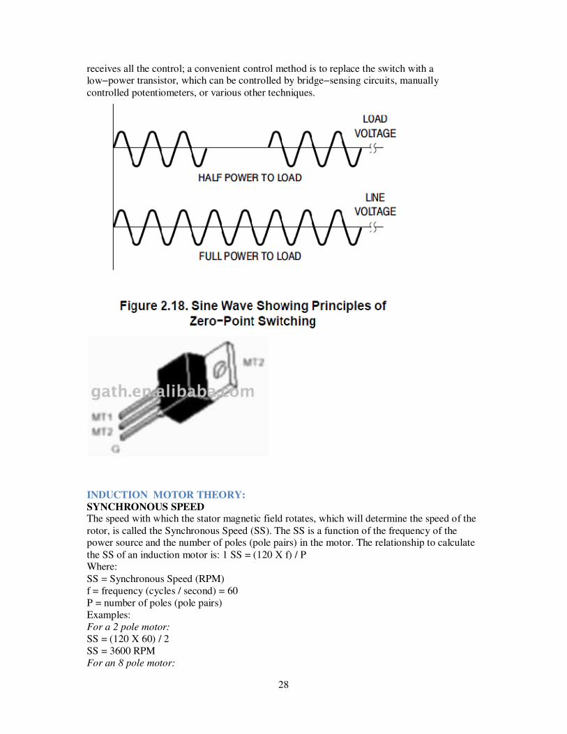
ZERO POINT SWITCHING
In addition to filtering, EMI can be minimized by zero−point switching, which is often
preferable. Zero−point switching is a technique where by the control element (in this case the
triac) is gated on at the instant the sine wave voltage goes through zero. This reduces, or eliminates, turn−on transients and the EMI. Power to the load is controlled by providing
bursts of complete sine waves to the load as shown in Figure 2.18. Modulation Can be on a random basis with an on−off control, or a proportioning basis with the proper type of
proportional control. In order for zero−point switching to be effective, it must Indeed be zero
point switching. If a triac is turned on with as little as 10 volts across it into a load of a
few−hundred watts, sufficient EMI will result to nullify the advantages of adopting
zero−point switching in the first place.
BASIC TRIAC AC SWITCHES
Figure 2.19 shows methods of using the triac as an on−off switch. These circuits are useful in
applications simplicity and reliability are important. As previously stated, there is no arcing
with the triac, which can be very important in some applications. The circuits are for resistive
loads as shown and require the addition of a (dv/dt) network across the triac for inductive
loads.
ZERO POINT SWITCHING TECHNIQUES
Zero−point switches are highly desirable in many applications because they do not generate electro−magnetic interference (EMI). A zero−point switch controls sine−wave power in such
a way that either complete cycles or half cycles of the power supply voltage are applied to the
load as shown in Figure 2.20. This type of switching is primarily used to control power to
resistive loads such as heaters. It can also be used for controlling the speed of motors if the
duty cycle is modulated by having short bursts of power applied to the load and the load
characteristic is primarily inertial rather than frictional. Modulation can be on a random
basis with an on−off control, or on a proportioning basis with the proper type of
proportioning control. In order for zero−point switching to be effective, it must be true
zero−point switching. If an SCR is turned on with an anode voltage as low as 10 volts and a
load of just a few hundred watts, sufficient EMI will result to nullify the advantages of going
to zero−point switching in the first place. The thyristor to be turned on must receive gate
drive exactly at the zero crossing of the applied voltage. The most successful method of
zero−point thyristor control is therefore, to have the gate signal applied before the zero
crossing. As soon as the zero crossing occurs, anode voltage will be supplied and the thyristor will come on. This is effectively accomplished by using a capacitor to derive a 90leading
gate signal from the power line source. However, only one thyristor can be controlled from this phase−shifted signal, and a slaving circuit is necessary to control the other SCR to get
full−wave power control. These basic ideas are illustrated in Figure 2.21. The slaving circuit fires only on the half cycle after the firing of the master SCR. This guarantees that only
complete cycles of power will be applied to the load. The gate signal to the master SCR
28
receives all the control; a convenient control method is to replace the switch with a
low−power transistor, which can be controlled by bridge−sensing circuits, manually
controlled potentiometers, or various other techniques.
INDUCTION MOTOR THEORY:
SYNCHRONOUS SPEED The speed with which the stator magnetic field rotates, which will determine the speed of the
rotor, is called the Synchronous Speed (SS). The SS is a function of the frequency of the power source and the number of poles (pole pairs) in the motor. The relationship to calculate
the SS of an induction motor is: 1 SS = (120 X f) / P Where:
SS = Synchronous Speed (RPM)
f = frequency (cycles / second) = 60
P = number of poles (pole pairs)
Examples:
For a 2 pole motor:
SS = (120 X 60) / 2
SS = 3600 RPM
For an 8 pole motor:

29
SS = (120 X 60) / 8SS = 900 RPM
MOTOR SLIP
The rotor in an induction motor cannot turn at the synchronous speed. In order to induce an
EMF in the rotor, the rotor must move slower than the SS. If the rotor were to somehow turn at SS, the EMF could not be induced in the rotor and therefore the rotor would stop.
However, if the rotor stopped or even if it slowed significantly, an EMF would once again be induced in the rotor bars and it would begin rotating at a speed less than the SS. The
relationship between the rotor speed and the SS is called the Slip. Typically, the Slip is expressed as a percentage of the SS. The equation for the motor Slip is: 2 % S = (SS – RS)
X100SS
Where:
%S = Percent Slip
SS = Synchronous Speed (RPM)
RS = Rotor Speed (RPM)
Example:
SS = 900 RPM
RS = 885 RPM
%S = (900 – 885) X 100
900
%S = 1.7% (or S = 0.017)
If the motor slip is known, the rotor speed can be expressed by the equation:
RS = (1 – S) X SS Example (using the information from above):
SS = 900 RPM %S = 1.7% (or S = 0.017)
RS = (1 – S) X SS RS = (1 – 0.017) X 900 RPM
RS = 885 RPM
EQUIVALENT CIRCUIT
To analyze the operating and performance characteristics of an induction motor, an
Equivalent Circuit can be drawn. We will consider a 3–phase, Y connected machine, the
The characteristics of an induction motor, the speed, current, starting torque, maximum
torque, the motor losses and efficiency can all be determined from an analysis of the
equivalent circuit Current and Power Factor To begin the analysis, the impedance of the
motor needs to be calculated. The impedance, ZRF, is the equivalent per phase impedance
seen by the stator across the motor gap.
6 ZRF = Z2 in parallel with Zx
= (R2/S + j X2 ) in parallel with jXx = (Rf + j Xf )
The total impedance, Z, is then: 7 Z = Z1 + ZRF
The stator current is: 8 I1 = V1 / Z
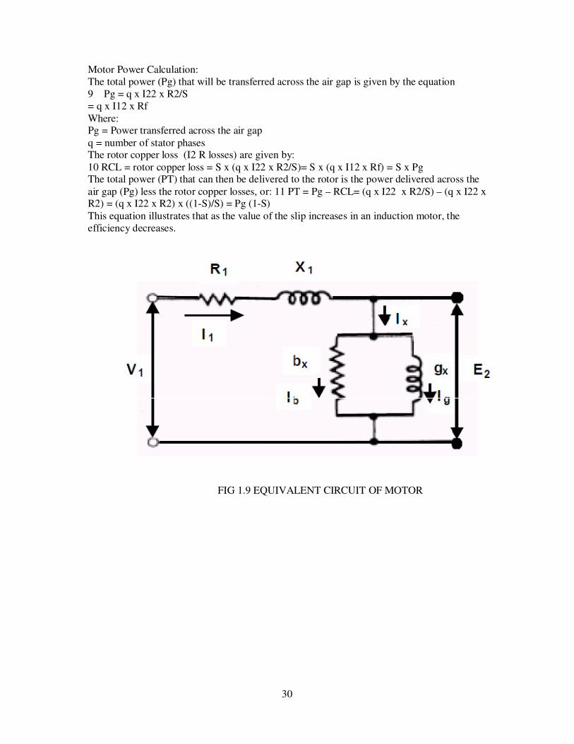
30
Motor Power Calculation:
The total power (Pg) that will be transferred across the air gap is given by the equation
9 Pg = q x I22 x R2/S
= q x I12 x Rf
Where: Pg = Power transferred across the air gap
q = number of stator phases The rotor copper loss (I2 R losses) are given by:
10 RCL = rotor copper loss = S x (q x I22 x R2/S)= S x (q x I12 x Rf) = S x Pg The total power (PT) that can then be delivered to the rotor is the power delivered across the
air gap (Pg) less the rotor copper losses, or: 11 PT = Pg – RCL= (q x I22 x R2/S) – (q x I22 x R2) = (q x I22 x R2) x ((1-S)/S) = Pg (1-S)
This equation illustrates that as the value of the slip increases in an induction motor, the
efficiency decreases.
FIG 1.9 EQUIVALENT CIRCUIT OF MOTOR
31
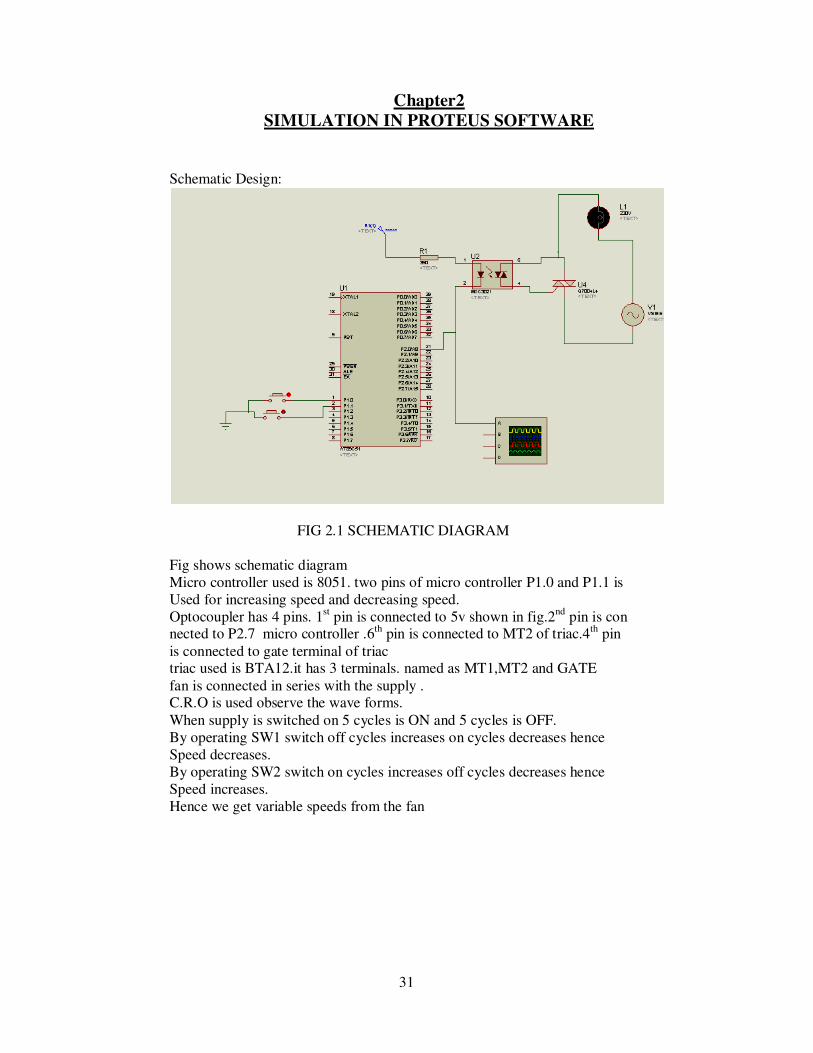
Chapter2
SIMULATION IN PROTEUS SOFTWARE
Schematic Design:
FIG 2.1 SCHEMATIC DIAGRAM
Fig shows schematic diagram
Micro controller used is 8051. two pins of micro controller P1.0 and P1.1 is
Used for increasing speed and decreasing speed.
Optocoupler has 4 pins. 1st pin is connected to 5v shown in fig.2
nd pin is con
nected to P2.7 micro controller .6th pin is connected to MT2 of triac.4th pin
is connected to gate terminal of triac triac used is BTA12.it has 3 terminals. named as MT1,MT2 and GATE
fan is connected in series with the supply . C.R.O is used observe the wave forms.
When supply is switched on 5 cycles is ON and 5 cycles is OFF.
By operating SW1 switch off cycles increases on cycles decreases hence
Speed decreases.
By operating SW2 switch on cycles increases off cycles decreases hence
Speed increases.
Hence we get variable speeds from the fan

32
Program :
#include<reg51.h>
sbit inc=P1^0;
sbit dec=P1^1;
sbit out=P2^0;
void delay(int i);
void delay1();
void main()
{ int i=10;
while(1)
{
if(inc==0)
{
while(inc==0);
i=i+1;
if(i>=20)
i=20;
}
if(dec==0)
{
while(dec==0);
i=i-1;
if(i<=0)
i=0;
}
out=1;
delay(i);
out=0;
delay(20-i);
}
}

33
void delay(int value)
{
int i;
for(i=0;i<value;i++)
delay1();
}
void delay1()
{
TMOD=0x01;
TL0=0x08;
TH0=0xdc;
TR0=1;
while(TF0==0);
TR0=0;
TF0=0;
}

34
Chapter3
HARDWARE DESIGN
Fig shows the hardware design of the project:
Whole project is embedded in the wooden box.
It consists of micro controller 8051
Optocoupler is 3021
Triac is BTA12 1-phase induction motor i.e., fan
CRO is used to observe the input cycles.
By controlling on-off cycles we can get variable speed.
Two switches are used one for increasing speed, other is for decreasing speed. Adapter is used to give supply to micro controller.

35

36
DATA SHEETS
37
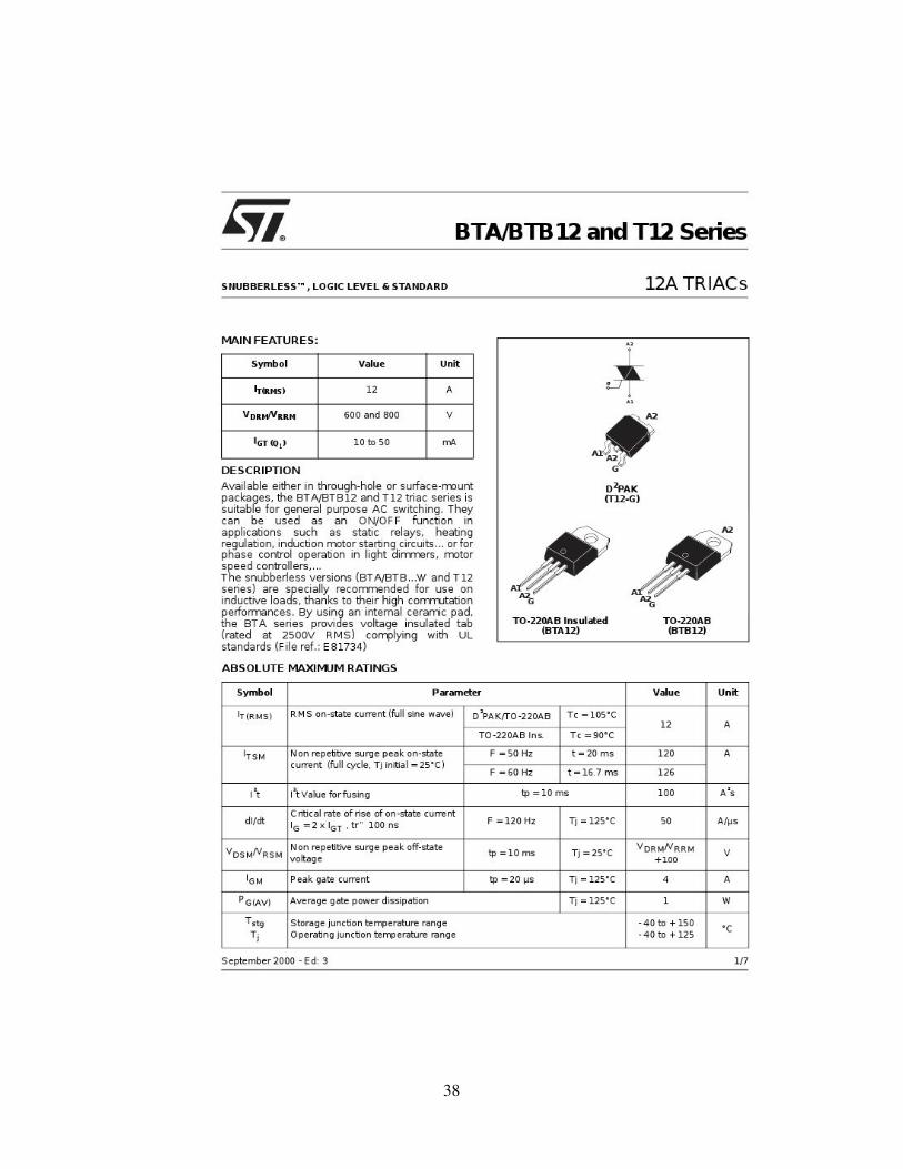
38

39

40
41
42

43

44
OUTPUT OBSERVATIONS
S.NO NO. OF ON
CYCLES
NO. OF OFF
CYCLES
OUTPUT
VOLTAGE
1 0 10 0
2 1 9 23
3 2 8 47
4 3 7 63
5 4 6 94
6 5 5 121
7 6 4 152
8 7 3 173
9 8 2 190
10 9 1 213
11 10 0 229

45
CHAPTER
REFERENCES
• Power electronics by bhimbra
• Power electronics by kanchandini
• Machines by J.B GUPTA
• www.google.com
• www.8051projects.com
• www.avrprojects.com
• www.microcontroller projects.com
CHAPTER
CONCLUSION: Due to zero voltage and zero current switching of thyristors the harmonics generated
by switching actions are reduced .Therefore i-phase induction motor speed control by
integral cycle control method has greater advantages such as less harmonic loss ,increased
efficiency.

46

47
CHAPTER
REFERENCES