instruction booi{ - james a. moorerjamminpower.com/pdf/bc-348-s.pdf · instruction booi{ for army...
TRANSCRIPT


INSTRUCTION BOOI{
FOR
ARMY AIR FORCES TECHNICAL ORDER No. 08-10-166
OPERATION AND MAINTENANCE
OF
RADIO RECEIVER BC-348-S AND
RADIO RECEIVER BC-224-L
RESTRICTED Notice:-This document contains information affecting the national defense of the United States within the meaning of the Espionage Act, 50 U. S. · C., 31 and 32, as amended. Its transmission or the revelation of its contents in an y manner to an unauthorized person is prohibited by law. (AR 380-5)
The information.. contained in re.stricted documents and the essential characterjstics of restricted material will not be communicated to the public or to the press, but may be given to any person known to be in the service of the United States and to persons of undoubted loyalty and discretion who are cooperating in Government work.
PUBLISHED BY AUTHORITY
OF
THE CHIEF SIGNAL OFFICER
APRIL 21, 1943

Destruction of
Abandoned Materiel in the Co,nbat Zone
In case it should become necessary to prevent the capture of this
equipment and when ordered to do so,
DESTROY IT SO THAT NO PART OF IT CAN BE SALVAGED, RECOGNIZED OR USED BY THE
ENEMY. BURN ALL PAPERS ANO BOOKS.
Means:-
1. Explosives, when provided.
2. Hammers, axes, sledges or whatever heavy object is readily available.
3. Burning by means of incendiaries such as gasoJine, oil, paper or wood.
4. Grenades and shots from available arms.
5. Where possible, and when time permits, bury all debris or dispose of it in streams or other bodies of water.
Procedure:-
1. Obliterate all identifying marks. Destroy nameplates ancl circuit label .
2. Demolish all panels, castings, switch- and instrument-boards.
3. Destroy all controls, switches, relays, connections and meters.
4. Rip out all wiring in electrical equipment. Smash gas, oil and water cooling systems in gasengine generators, etc.
5. Smash every electrical or mechanical part whether rotating, moving or fixed.
6. Break up all operating instruments such as keys, phones, microphones, etc.
7. Destroy all classes of carrying cases, straps, containers, etc.
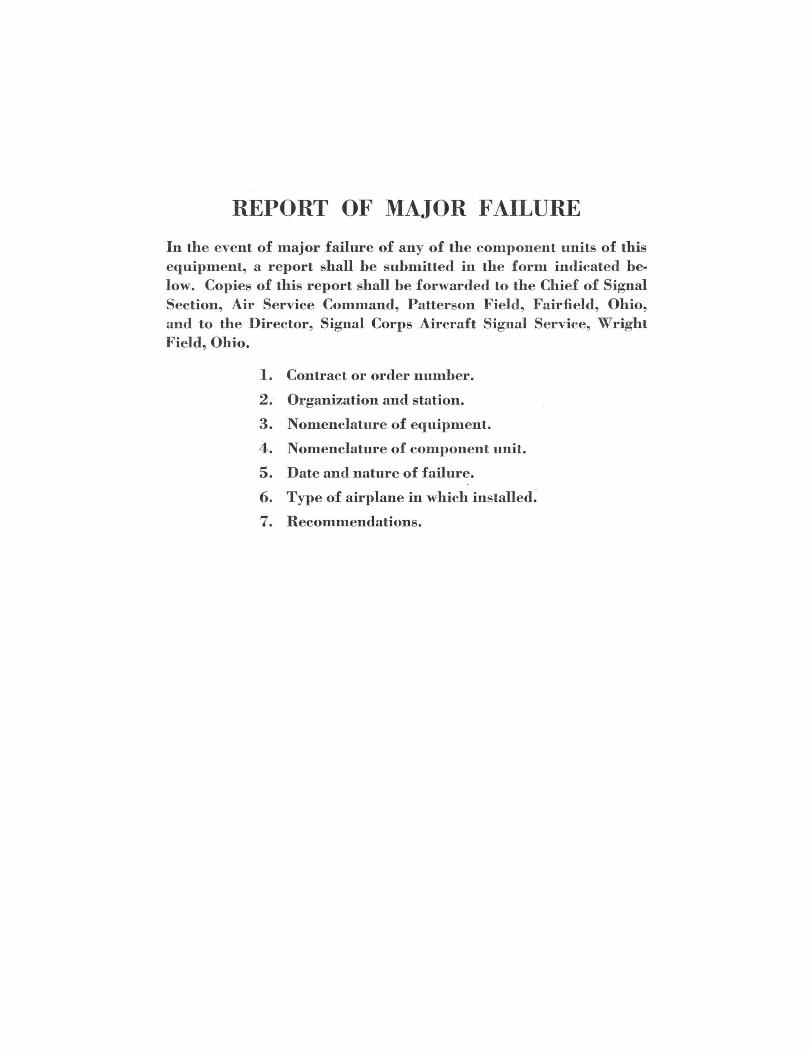
REPORT OF MAJOR FAILURE
In the event of major failure of any of the component units of this equipment, a report shall he submitted in the form indicated below. Copies of this report shall he forwarded to the Chief of Signal Section, Air Service Command, Patterson Field, Fairfield, Ohio, and to the Director, Signal Corps Aircraft Signal Service, Wright Field, Ohio.
1. Contract or order number.
2. Organization and station.
3. Nomenclature of equipment.
4. Nomenclature of component unit.
5. Date and nature of failure.
6. Type of airplane in which installed~
7. Recommendations.

l. GENERAL
2. INSTALLATION
TABLE OF CONTENTS
SECTION I
DESCRIPTION AND INSTALLATION
!'AGE
. .............. . ... . . ... ... .. .. ......... . . . .... 1
..... ...... ...... . .... . .. ............... ....... 1
a. Mounting . . . . . . . . . . . . . . . . . . . . . . . . . . . . . . . . . . . . . . . . . . . . . . . . . . . . . . . . . . . . . . . . . . . . . . . . . . . . . . . . 1
b. Power Connections . . . . . . . . . . . . . . . . . . . . . . . . . . . . . . . . . . . . . . . . . . . . . . . . . . . . . . . . . . . . . . . . . . . . . . . . 1
c. Radio Transmitter Connections ... . .. . . .. . .. . . .
d. Output Connections . . . . . . . . . . . . . . . . . . . . . . . . . . . . . . . . . . . . . . . . . . . . . . . . . . . . . . . . . . . . . . . . . . . . . . . . 1
e. Bonding and Shielding. . . . . . . . . . . . . . . . . . . . . . . . . . . . . . . . . . . . . . . . . . . . . . . . . . . . . . . . . . . . . . . . . . . . . . 2
f. Mounting of Radio Receiver . . . . . . . . . . . . . . . . . . . . . . . . . . . . . . . . . . . . . . . . . . . . . . . . . . . . . . . . . . . . . . . . . 2
g. Safety Wire . . . . . . . . . . . . . . . . . . . . . . . . . . . . . . . . . . . . . . . . . . . . . . . . . . . . . . . . . . . . . . . . . . . . . . . . . . . . . . . 2
h. Ground .. . .. .. .. . ... .. .. . ....... . .................. ... 2
i. Antenna ..... ... . . ............................. .. ...... 2
j. Adjustment of Input Alignment Capacitor. . . . . . . . . . . . . . . . . . . . . . . . . . . . . . . . . . . . . . . . . . . . . . . . . . . . . . 2
3. PRELIMINARY CHECK
SECTION II
PREPARATION FOR USE
. ... ........................................... 3
4. POWER CONNECTIONS . . . . . . . . . . . . . . . . . . . . . . . . . . . . . . . . . . . . . . . . . . . . . . . . . . . . . . . . . . . . . . . . . . . . . . . . . . 3
5. OPERATING TEST ............ . . ... ............ .. .... . .. . .... . ......•. .......... . ... .. ... .•. ... . 3
6. OPERATING PROCEDURE
SECTION III
OPERATION
......... .. .... .. ........ . ................... . . ......... . .. .. .. .. ........ 5
a. Controls . . . . . . . . . . . . . . . . . . . . . . . . . . . . . . . . . . . . . . . . . . . . . . . . . . . . . . . . . . . . . . . . . . . . . . . . . . . . . . . . . . 5
vii

TABLE OF CONTENTS {Continued)
PAHACRA P H P ACE
SECTION III-OPERATION (Continued)
6. O PERATING PROCEDURE · ( CONTINUED) ... . .... . . . .. . . .......•....... •. . .. ..... • . •• ....... • .. ... . . .. 5
b. Modulated Signal Reception . . . . . . . . . . . . . . . . . . . . . . . . . . . . . . . . . . . . . . . . . . . . . . . . . . . . . . . . . . . . . . . . . . 5
c. C-W Reception . . . . . . . . . . . . . . . . . . . . . . . . . . . . . . . . . . . . . . . . . . . . . . . . . . . . . . . . . . . . . . . . . . . . . . . . . . . . . 5
SECTION IV
MAINTENANCE
7. ALIGNMENT OF 1-F AMPLIFIER . . •• ....• • . • . . .. . . . . . . . .....• • .. . . . . ... .. .. . . . . ....... • • . ... .. .. ... . 6
8 . TEST AND A DJUST M ENT OF CRYSTAL FILTER. . . . . . . . . . . . . . . . . . . . . . . . . . . • . . . • • . . . • . . • . . . • • . • • . . . . . . . . 6
9. CHEC K AND ALIGNMENT OF C -W OSCI LLATOR . ... .... . ... . ....... . . . .... . .......... .. . . .. • . .•. . . . .... 6
10. ALIGNMENT OF R-F AMPLIFIER AND O SCILLATOR. . . . . . . . . . . . . . . . . . . . . . . . . . . . . . . . . . • . . . . . . . . . . . . . . . . . . 7
SECTION V
SUPPLEMENTARY DATA
TABLE OF R EPLACEABLE P ARTS FOR RADIO RECEIVERS BC-348-S AND BC-2 2 4 -L .. . .... . .. .. . ... . .. . . .. . .. . 9

LIST OF ILLUSTRATIONS
FIGURE PA.CS
1. RADIO RECEIVER BC-348-S, FRONT VIEW . . . . . . . . . . . . . . . . . . . . . . . . . . . . . . . . . . . . . • . . . . . . . . . . . . . . . . . . . . . . x
2. RADIO RECEIVER BC-348-S, CORDING DIAGRAM . . . . . . . . . . . . . . . . . . . . . . . . . . . . . . . . . . . . . . . . . . . . . . . . . . . . . . 2
3. RADIO RECEIVER BC-348-S, TOP VIEW OF CHASSIS . . . . . . . . . . . . . . . . . . . . . . . . . . . . . . . . . • . . . • • . . • • . . . . • • . . 6
4. RADIO RECEIVER BC-348-S, REAR VIEW OF CHASSIS. . . . . . . . . . . . . . . . . . . . . . . . . . . . . . . . . . . . . . . . . . . . . . . . . . 7
5. RADIO RECEIVER BC-348-S, BOTTOM VIEW OF CHASSIS . . . . . . . . . . . . . . . . . . . . . . . . . . . . . . . . . . . . . . . . . . . . . . . 8
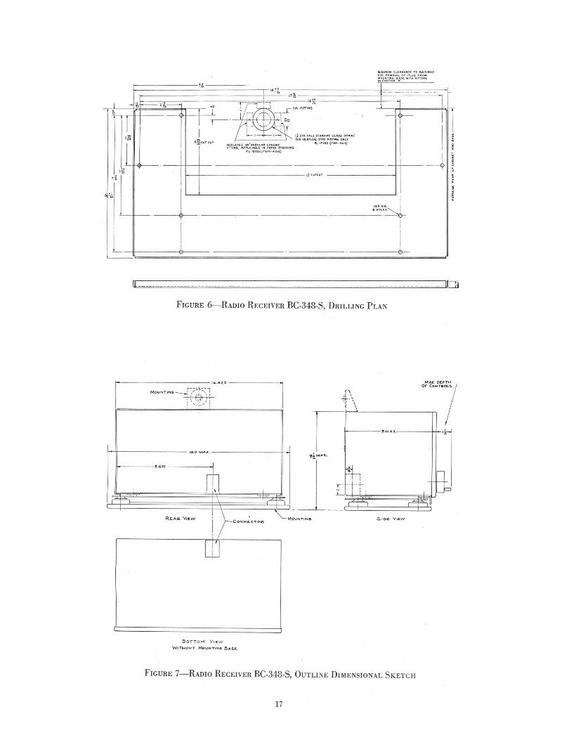
6. RADIO RECEIVER BC-348-S, DRILLING PLAN . . . . . . . . . . ............ .. .......... .. .. .. .. • ... .. ........ 17
7. RADIO RECEIVER BC-348-S, OUTLINE DIMENSIONAL SKETCH ... . ...... ... ... .... .. ...... .. .. . . ........ 17
8 . RADIO RECEIVER BC-348-S, SCHEMATIC DIAGRAM . .... ... . . . • ........ .. . . ....... . - ........ •• . . ...... 19
9. RADIO RECEIVER BC-224-L, SCHEMATIC DIAGRAM • ...•...•....... . . . ... . .... ... •... ..... . ... .. . ..... 21
ix
N I
~
~---0
I.() o----
<O o---
.. .. ..
...... ---o
('\J '---------0
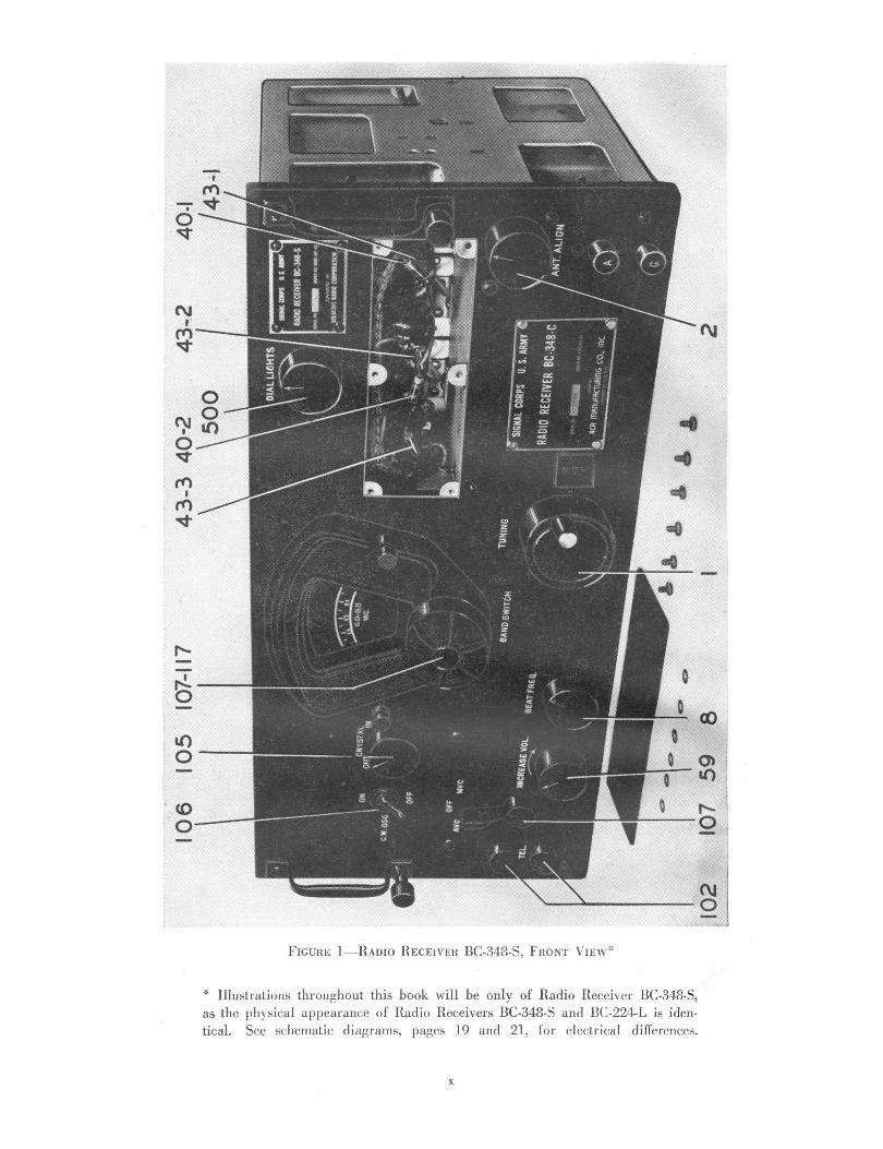
FIGURE 1-RADIO RECEIVER BC-348-S, FRONT Vmw"·
* Illustrations throughout this book will be only of Radio Receiver BC-348-S, as the physical appearance of Radio Receivers BC-348-S and BC-224-L is identical. See schematic diagrams, pages 19 and 21, for electrical differences.
x
Section I Pars. 1-2
INSTR,UCTION · BOOK Fo ..
OPERATION AND MAINTENANCE
of R,ADIO · R ,ECEIVER . BC-348-S
and R,ADIO R,ECEIVER BC-224-L
SPECIAL NOTICE
Radio Receivers BC-348-S and BC-224-L have been converted from other production models (Radio Receivers BC-348-C and BC-224-C, respectively) by Belmont Radio Corporation, Chicago, Illinois. On equipments produced under this conversion, a name plate appears on the upper right of the panel of each of both types of receiver, identifying each equipment as Radio Receiver BC-348-S and Radio Receiver BC-224-L, respectively, in addition to the name plate for the original receivers-Radio Receivers BC-348-C and BC-224-C -which appears' on the bottom right of the panel.
Although this instruction book covers both Radio Receivers BC-348-S and BC-224-L, only the former will be referred to throughout the book for convenience in reference, as the two equipments are essentially identical. See schematic diagrams, pages 19 and 21, for differences.
Best,·icted SECTION I
DESCRIPTION AND INSTALLATION
1. GENERAL
Radio Receiver BC-348-S is a locally-controlled, 8-tube, 6-band superheterodyne receiver for use in U. S. Army aircraft and covers the frequency ranges of 200 kc to 500 kc and 1.5 to 18.0 megacycles. The receiver is not intended for remote control, and no features or units have been prqvided for remote operation. This radio receiver is capab le of voice, tone and c-w reception with manual or automalic volume control. When equipped with tubes, dial lights and fuse, and with the antenna, ground and 28-volt". primary power source connections properly made, it becomes a complete and operative equipment by the addition of a headset, as all coils and the high-voltage power supply unit are built in. See Figure 2 for proper connection of terminals No. 2 and No. 6.
The most important considerations necessary for the successful installation and operation of this receiver are as follows:
2. INSTALLATION
a. Mounting Mount the receiver on a plane surface, allow
ing sufficient clearance on all sides to permit free action of the shock absorber mountin::". The mounting should be permanently attached to the rigid mem-
hers of the plane. The drilling plan of the mounting is shown in Figure 6.
b. Power Connections Separate pairs of leads to the 28-volt primary
power source may be us~d. See Figure 2.
c. Radio Transmitter Connections Provisions have been made for the protection
of this receiver when the associated radio transmitter is being used. Wire leads from plug terminals 2 and 6 to con tacts on the transmitter relay. If the transmitter is removed from the installation , the wires from plug terminals 2 and 6 must be connected for the radio receiver to operate.
d. Output Connections The output of this receiver has been brought
to plug terminals 1 and 5. Leads .from these terminals should be wired to the interphone system or as otherwise desired. If the output is desired only at the receiver, it should be taken dire::tly from the phone jack and no connections made to plug terminals 1 and 5. Normal connection is to the 4000-ohm tap marked 4 on the output transformer case. Access to a 300-ohm tap is provided at the terminal marked 2.
*Radio Receiver BC-224-L requires a 14-volt primary power source.

Radio Receiver BC-348-S Par. 2
e. Bonding and Shielding At the time of installation of this equipment,
make certain that the engine ignition system, generator and other possible causes of disturbance are properl y shielded and that bonding of metal par ts is carefully carried out.
f. Mo unting of Radio R eceiver When proper wiring connections have been
made, place the receiver on its mounting with the st~ds on the bottom of the cabinet entering the slots of the mounting. See that the cabinet is well down on the mounting and that all four studs are fully seated, then push the cabinet towards the rear and fasten by means of the snapslides on the lower front corners of the cabinet.
g. Safety Wire Pass safety wire through the holes of the snap
slide assemblies, being careful that the wires are not twisted too tightl y.
h. Ground Connect the gro und-binding post G by a short,
direct, low-resistance lead to some grounded metal portion of the plane and solder at that point, if practicable. The lead should have enough slack to prevent vibration being transmitted to the receiver.
i. Antenna
The antenna-circuit aligning capacitor is such that the antenna circuit can be properly aligned when using antennas that range in effective capacitance from 50 to 200 micromicro-farads . However, satisfactory performance will be obtained in practically any type of mast, fi xed or trailing wire antenna, although in extreme cases, i.e., very short mast or very long trail· ing wire, optimum setting of the "antenna alignment" may not be obtained. In general, the most effective antenna is one whose length away from the grounded metal fu selage is the greatest. P lace the receiver as near as possible to the lead-in insulator and connect it from the insulator to the antenna binding post A by a copper wire. The lead should have enough slack to preven t vibration being transmitted to the receiver.
j. Adjustment of Input Alignment Capacitor
With the receiver A VC-OFF-MVC switch in the MVC position, the band switch on Band 2, and using the tuning control, tune in a signal at approximately 3.5 me to maximum signal strength. Reduce volume by means of the volume control knob until the signa l is just audible. Adjust the ANTENNA ALIGN· MENT control to give maximum volume.
OUTPUT TRANSMITTER RELAY (TO INTERPHONE) (CLOSED FOR)
PLUG
\. Ir REQUIRED j RECE:IVING
+ 200V FOR AUXILIARY GROUND EQUIPMENT WHEN NtEDED
B£TW£EN ,r2 AND #5 11 20MA. (MAX) ~
IF" TRANSMITTER IS NOT THESE: LE:AOS NOT TO BE INSTALLED THESE LEADS ARE
CON NECTED TO PLUG If' NOT TO BE CONNECTED TO THE PLUG OUTPUT IS DESI RED AT A JUMPER AT THE PLUG
RECEIVER ONLY. SHOULD BE USED TO CONNECT TERMI NALS ¥2 & °'6
SHIEL DI NG TO BE ;_ CONNECTED TO TERM . .S
TO TERM. °*5 TO TERM."'I TO TERM. *6 TO TERM . .,2
TO TERM."'3 TO TERM. *°4 TO TERM . fl TO TERM. #17
THESE LEADS JOINED AT BATTERY OR MAIN BUS, AND NOT AT PLUG
THESE LEADS MAY BE . [ J. THESE LEADS MAY Ll REPLACED BY A SINGLE ---==-c;-6 BE REPLACED BY A Q ()
CONDUCTOR SINGLE CONDUCTOR -
+ POWER SOURCE
FIGURE 2-RADIO RECEIVER BC-348-S, CORDING DIAGRAM
2

Section II Pars. 3.5
SECTION II
PREPARATION FOR USE
3. PRELIMINARY CHECK Radio Receiver BC-348-S is a self-contained unit,
having its high-voltage power supply and all coil sets built in.
a. Before installing the tubes, check them with the required tube checker.
b. Be sure that the proper tubes, well pushed down and firmly seated in their sockets, are installed, that the tube shield is properly seated and that grid caps fit tightly on the tubes.
c. Check dial lights and fuses and see that they are properly and securely placed.
d. Make sure that the leads to the dynamotor are properly connected at the dynamotor terminal strip and that the screws holding them in place are tight. No other precautions are necessary.
4. POWER CONNECTIONS Power to the radio receiver is controlled by the
receiver AVC- OFF-MVC switch. The table below shows the power conn e::: tions in conjunction with this receiver switch.
The screen grid voltage supply leads are carried out of the receiver through the power plug to the keying rel-ay of the associated radio transmitter where the circuit is opened when actually transmitting.
5. OPERATING TEST When the receiver has been completely installed,
an operating test should be made as follows:
a. Plug the headset into the TEL jack. Set the
receiver switch to MVC. The dynamotor should start
and after the tubes have warmed up (aproximately
30 seconds), the volume control knob should be ad
vanced until a slight background noise is heard. Set
the BAND SWITCH to the fr equency band in which test
signals are available.
b. Using the TUNING knob and with reference to
the calibrated scale on the dial, tune in the desired sig
nal. NOTE: All tunin6 should be done on MVC with
the volume contro l advanced only enough to give the
desired signal strength. In the absence of a signal ,
the setting of the volume control can be judged by the
loudness of th e background noise. On MVC, with the
volume contro l set at maximum, very strong earner
waves will block the receive r and intelligible signals
cannot be received.
c. Set the receiver switch to A vc. The desired sig
nal should still be heard.
POWER CONNECTIONS
Receiver Switch D ial L ight Circuit
Position Rheostat Connection
OFF MIN No power supplied
to receiver
OFF MAX No power supplied
to receiver
Filaments ON, dyna-AVC MIN motor ON, dial
lights OUT
Filaments ON, dyna-AVC MAX motor ON, dial
lights FULL ON
MVC MIN Filaments ON, dyna-
motor ON, dial lights OUT
MVC MAX Filaments ON, dyna-
motor ON, dial lights FULL ON
3

Radio Receiver BC-348-S Par. 5
d. With the BEAT FREQ adjustment at zero beat position ( arrow on knob pointing up) , turn the C-W
osc switch to the ON position. An audible beat note should be heard which should vary in pitch when the BEAT FREQ adjustment is changed.
e. With the FREQ c-w osc still ON, throw the
CRYSTAL filter switch to IN. Noise should be greatly
reduced and the signal can be tuned out by a much
smaller movement of the tuning con trol knob than
when the CRYSTAL filter switch is in the OUT position.
f. Turn the DIAL LIGHT rheostat and observe if control of illumination is secured with both dial lights functioning_
g. Make a pre-flight check, with the airplane engine running. An increase of background noise when the engine starts indicates imperfect shielding or bonding, faulty generator regulator, faulty generator, open filter capacitors or a combination of these faults.
h. Always turn the receiver switch to the OFF position when the receiver is not to be used.

Section III Par. 6
SECTION III
OPERATION
6. OPERATING PROCEDURE
a. Controls
(i) Antenna and Ground Binding Posts The antenna is connected to the binding post
marked A, and the ground lead to the binding post marked G.
(ii) ANT ALIGN Control This control is a variable capaci tor for align
ing the input circuit to a given antenna. This adjustment should be made with the receiver tuned to approximately 3.5 me in Band 2.
(iii ) T UNING Control This control varies the setting of the 4 -gang
variable tuning capacitor.
( iv ) BAND SWITCH Control This control selects the desired frequency band
as indicated on the dial mask.
( v) DIAL LIGHTS Control This knob controls the intensity of dial illumi
nation and is provided with an OFF position.
(vi ) c-w osc Switch This toggle switch controls the operation of
the c-w oscillator as well as the AVC time constan t for c-w reception.
(vii) CRY ST AL Switch This control permits the insertion of an i-f
crystal filter when extreme selectivity is desired.
( viii ) BEAT FREQ Control This control permits vernier adjustment of the
c-w oscillator frequency and, in tuning, it should be set near the zero bea t position (arrow on knob pointing up).
(ix ) INCREASE VOL Control This control is for sensitivity adjustment on
MVC operation and output level adjustment on AVC
operation. When switching from MVC to AVC or vice versa, it will generall y be necessary to readjust this control to maintain a given volume level, as only under certain conditions of signal strength will the volume level remain unchanged.
(x) AVC-OFF-MVC Switch . This three-posi tion switch in the OFF p os1t10n
removes all power from the receiver. In the MVC
position the receiver is operative with manual volume control, while in the AVC position the automatic volume control is fun ctioning.
( xi) TEL Jacks These are open circuit jacks providing con
nections to the headset.
5
b. Modulated Signal Reception (i) Throw the AVC-OFF-MVC switch to MVC
and set other switches and controls as follows: C-W OSC-OFF
CRYSTAL Filter- OUT ANT ALIGN set as in the initial installation ad
justment.
(ii) Set the BAND SWITCH to the desired frequency band and adjust the TU NING control to the desired frequency with reference to the dial calibration. It is of greatest importance that this tuning be accomplished with the receiver switch in the MVC position.
(iii) Increase the VOL con trol until the desired signal is heard or the background noise attains a fair level.
(iv) Adjust the TU ING control until maximum output from the desired signal is obtained. This insures correct alignment or proper tuning of the receiver.
( v) If automatic volume control is desired, switch to the AVC position and readjust the VOL control for the desired output level.
(vi) NOTE : The AVC should not be employed while tuning in a signal. Tuning should always be done in the MVC position and with the volume control advanced only as far as required for a comfortable output level.
c. C-W Reception
(i) The procedure is the same as outlined above with the excep tion that the c-w osc switch is ON and tuning accomplished with the BEAT FREQ control set near the zero beat position (arrow on knob pointing up ).
(ii ) After tuning in the desired signal, the BE AT FREQ control ma y be varied and the frequency of the beat note adjusted as desired.
.( iii ) Automatic vo lume control may be employed for c-w reception by switching to the AVC position and readjusting the volume control.
(iv) When extreme selectivity is desired to minimize interference, the CRYSTAL filter is switched IN. A slight readjustment of the tuning and beat frequency controls may be required to secure the desired beat note frequency.
( v) NoTE: The crystal band pass filter is intended primarily for use in c-w reception . However, the added selectivity may at times prove helpful in receiving modulated signals through heavy interference.

Radio Receiver BC-348-S Pars. 7-9
SECTION IV
MAINTENANCE
7. ALIGNMENT OF 1-F AMPLIFIER
The 4th i-f transformer (100) is slightly overcou pied with the resultant response peaks approximately 5 kc each side of 915 kc. Connect the modu-
lated test oscillator to the grid of Tube VT-93. Adjust
primary and secondary tuning cores of the 4th i-f
transformer so that even peaks are obtained at ap
proximately 920 kc and 910 kc with the sli ght dip
between them at 915 kc. Visual adjustm ent may also
be made with a cathode-ray oscilloscope. After ad-
252 106 VT-86 255 2 51 VHB
8. TEST AND ADJUSTMENT OF CRYSTAL FILTER
Connect a microammeter with a range of approximately 200 microamperes in series with the cathode return of the AVC vo lume control (59-B orange lead ) . Throw the CRYSTAL switch (105) to the IN position and with an unmodulated 915 kc input from the test oscillator find the resonance peak of the crystal by slightly retuning the test oscillator until maximum deflection is indicated on the microammeter.
The band width with an input voltage ratio of 10 X
VT·91 VT-86 500 103 VT-86
FIG URE 3- RAoro RECEIVER BC-348-S, Top Vrnw OF CHASSIS
justmen t of the 4th i-f transformer, couple the tes t
oscillator to the grid of the converter Tube VT-91 and
adjust primary and secondary cores of the 3rd i-f ( 99_),
2nd i-f (97), crystal filter (96) and 1st i-f trans
former (95) to resonance. A 4000-ohm output meter
is plugged into the phone jack (102) for observing.
Do not readjust the 4th i-f transformer.
6
is adjusted to approximately 2 kc by adjustment of
the phasing trimmer (7).
9. CHECK AND ALIGNMENT OF C-W OSCILLATOR The c-w oscillator (98) is checked and adjusted
by coupling the 915 kc input (modulation off) to the grid of the converter Tube VT-91 and switching the c-w osc ON. With the beat frequency control set

at mid-position, the c-w oscillator ~nductor tuning core
is a1justed for zero beat.
10. ALIGNMENT OF R-F AMPLIFIER AND OSCILLATOR
For a genera l alignment, start with Band No. 1
and proceed as in the table below. Use a 400-cycle
Band Freq. Range
Alignment . No. Frequency
l 500-200 kc J 500 kc t 200 kc
2 3.5- 1.5 me 3.5 me
3 6.0- 3.5 me 6.0 me
4 9.5- 6.0mc 9.5 me
5 13.5- 9.5 me ]3.5 me
6 18.0-13.5 me 18.0 me
Osc.
6-1 66
6-2 6 •) -.::,
6-4
6-5
3-6
Section IV Pars. 9-10
modulated test oscillator connected between antenna
and ground through a 100-mmf dummy antenna. A
4000-ohm output meter is plugged into the phone
jack (102) for observing. Adjust the oscillator fre
quency to the dial scale at the Alignment Frequency
indicated in the table and then adjust 1st det., r-f and
antenna trimmers as shown.
Trimmers
Det. R-F Ant.
37-2 37-1 65
5-5 5-3 2 fr
3-4 32 3-1
5-6 5-4 5-1
3-5 3-3 3-8
4-3 4-2 4-1
''Antenna aligning capaci ty. Refer to the schematic diagrams, Figures 8 and 9, and marked photographs for location. The alignment controls for the various bands are numbered on the chassis adjacent to the control. Controls for band 1 are marked 1; those for 2 are marked 2, etc.
FIGURE 4--RADIO RECEIVER BC-348-S, REAR VIEW OF CHASSIS
7

Radio Receiver BC-348-S
7 1·0 l·C l·B l·A
38·3 39·1 VT·48 502 66
FIGURE 5 - RADIO RECEIVER BC-348-S, BOTTOM VIEW OF CHASSIS
8

Reference Na ,ne Nitmber
1-Ai 1-B Capacitor 1-C 1-D
2 Capacitor
3-1 Capacitor
3-2 Capacitor
3-3 Capacitor
3-4 Capacitor
3-5 Capacitor
3-6 Capacitor
3-7 Capacitor
3-8 Capacitor
4-1 Capacitor
4-2 Capacitor
4-3 Capacitor
5-3 Capacitor
5-4 Capacitor
5-5 Capacitor
5-6 Capacitor
6-1 Capacitor
6-2 Capacitor
6-3 Capacitor
6-4 Capacitor
6-5 Capacitor
7 Capacitor
8 Capacitor
9-1 Capacitor
9-2 Capacitor
9-3 Capacitor
SECTION V SUPPLEMENTARY DATA
TABLE OF REPLACEABLE PARTS FOR RADIO RECEIVERS BC-348-S AND BC-224-L
Description Function
I A. Section 13.5 to 331.6 mmf B. Section 13.5 to 331.6 mmf Main tuning C. Section 13.5 to 331.6 mmf
1. D. Section 13.5 to 331.6 mmf
Air trimmer 50 mmf max. Ant. aligning
Air trimmer 50 mmf max. Ant. trimmer
Air trimmer 50 mmf max. R-F trimmer
Air trimmer 50 mmf max. R-F trimmer
Air trimmer 50 mmf max. Det. trimmer
Air trimmer 50 mmf max. Det. trimmer
Air trimmer 50 mmf max. Osc. trimmer
Air trimmer 50 mmf max. Ant. trimmer
Air trimmer 50 mmf max. Ant. trimmer
Air trimmer 50 mmf max. Ant. trimmer
Air trimmer 50 mmf max. R-F trimmer
Air trimmer 50 mmf max. Det. trimmer
Air trimmer 25 mmf max. R-F trimmer
Air trimmer 25 mmf max. R-F trimmer
Air trimmer 25 mmf max. D et. trimmer
Air trimmer 25 mmf max. Det. trimmer
Air trimmer 25 mmf max. Osc. trimmer
Air trimmer 25 mmf max. Osc. trimmer
Air trimmer 25 mmf max. Osc. trimmer
Air trimmer 25 mmf max. Osc. trimmer
Air trimmer 25 mmf max. Osc. trimmer
Air trimmer 10 mmf max. Crystal filter adjustment
Air trimmer 10 mmf max. C-W osc. adjustment
Mica 500 volts d-c .01 mf ± 10% with leads 1st R-F cathode by-pass
Mica 500 volts d-c .01 mf ± 10% with leads 1st R-F screen by-pass
Mica 500 volts d-c .01 mf ± 10% with leads 2nd R-F cathode by-pass
9

TABLE OF REPLACEABLE PARTS FOR
RADIO RECEIVERS BC-348-S AND BC-224-L (Continued)
Reference Name Description Fttnc tion Nttmber
9-4 Capacitor Mica 500 volts d-c .01 mf ± 10% with leads 2nd R-F screen by-pass
9-5 Capacitor Mica 500 volts d-c .01 mf ± 10% with leads 1st Det. screen by-pass
9-6 Capacitor Mica 500 volts d-c .01 mf ± 10% with leads 1st 1-F transformer by-pass
9-7 Capacitor Mica 500 volts d-c .01 mf ± 10% with leads Crystal transformer by-pass
9-9 Capacitor Mica 500 volts d-c .01 mf ± 10% with leads 1st 1-F plate by-pass
9-10 Capacitor Mica 500 volts d-c .01 mf ± 10% with leads 2nd 1-F transformer by-pass
9-12 Capacitor Mica 500 volts d-c .01 mf ± 10% with leads C-W osc. plate by-pass
9-13 Capacitor Mica 500 volts d-c .01 mf ± 10% with leads Plug terminal by-pass
9-14 Capacitor Mica 500 volts d-c .01 mf ± 10% with leads A.V.C. by-pass
9-15 Capacitor Mica 500 volts d-c .01 mf ± 10% with leads 3rd 1-F transformer by-pass
9-16 Capacitor Mica 500 volts d-c .01 mf ± 10% with leads 3rd 1-F cathode by-pass
9-17 Capacitor Mica 500 volts d-c .01 mf ± 10% with leads Heater by-pass
9-18 Capacitor Mica 500 volts d-c .01 mf ± 10% with leads Battery by-pass
10-1 Capacitor Mica 500 volts d-c .01 mf ± 10% with lugs Ant. coil by-pass
10-2 Capacitor Mica 500 volts d-c .01 mf ± 10% with lugs 1st H-F plate
10-3 Capacitor Mica 500 volts d-c .01 mf ± 10% with lugs R-F coil by-pass
10-4 Capacitor Mica 500 volts d-c .01 mf ± 10% with lugs 2nd R-F plate
11-1 Capacitor Mica 500 volts d-c .01 mf ± 10% with lugs Osc. plate
11-2 Capacitor Mica 500 volts d-c .01 mf ± 10% with lugs 1st Det. cathode by-pass
12-1 Capacitor Mica 500 volts d-c .005 mf ± 10% with leads Audio transformer secondary by-pass
12-2 Capacitor Mica 500 volts d-c .005 mf ± 10% with leads Antenna blocking
13 Capacitor Mica 500 volts d-c 390 mf ± 1.2% with leads Osc. series
14 Capacitor Mica 500 volts d-c 2240 mmf ± 3% with leads Osc. series
15-1 Capacitor Mica 500 volts d-c 1500 mmf ± 10% with leads Audio coupling
15-2 Capacitor Mica 500 volts d-c 1500 mmf ± 10% with leads Audio transformer primary shunt
16 Capacitor Mica 500 volts d-c 670 mmf ± 1.2% with leads Osc. series
17 Capacitor Mica 500 volts d-c 130 mmf ± 5% with leads Osc. series
10

TABLE OF REPLACEABLE PARTS FOR
RADIO RECEIVERS BC~348-S AND BC-224-L (Continued)
Reference Name Description Function Number
18-1 Capacitor Mica 500 volts d-c 500 mmf ± 5% with leads 1st I-F secondary tuning
18-2 Capacitor Mica 500 volts d-c 500 mmf ± 5% with leads 1st I-F secondary tuning
19 Capacitor Mica 500 volts d-c 285 mmf ± 5% with leads Crystal transformer tuning
20-1 Capacitor Mica 500 volts d-c 260 mmf ± 5% with leads 2nd I-F primary tuning
20-2 Capacitor Mica 500 volts d-c 260 mmf ± 5% with leads 2nd I-F secondary tuning
20-3 Capacitor Mica 500 volts d-c 260 mmf ± 5% with leads 3rd I-F secondary tuning
21-1 Capacitor Mica 500 volts d-c 250 mmf ± 5% with leads 1st I-F primary tuning
21-2 Capacitor 'Mica 500 volts d-c 250 mmf ± 5% with leads 3rd 1-F primary tuning
22-1 Capacitor Mica 500 volts d-c 240 mmf ± 5% with leads C-W osc. tuning
22-2 Capacitor Mica 500 volts d-c 240 mmf ± 5% with leads 2nd Det, by-pass
23 Capacitor Mica 500 volts d-c 170 mmf ± 1.2% with leads Osc. series
24-1 Capacitor Mica or Ceramic 500 volts d-c 155 mmf ± 1.8% Ant. series with leads
24-2 Capacitor Mica or Ceramic 500 volts d-c 155 mmf ± 1.8% R-F series - with leads
24-3 Capacitor Mica or Ceramic 500 volts d-c 155 mmf ± 1.8% Det, series with leads
25 Capacitor Mica or Ceramic 500 volts d-c 25 mmf ± 10% Ant. shunt with leads
26-1 Capacitor Mica 500 volts d-c 150 mmf ± 5% with leads C-W osc, grid
26-2 Capacitor Mica 500 volts d-c 150 mmf ± 5% with leads 4th I-F secondary tuning
27 Capacitor Mica 500 volts d-c 135 mmf ± 1.2% with leads Osc, series
28-1 Capacitor Mica 500 volts d-c 135 mmf ± 2% with leads Ant, series
28-2 Capacitor Mica 500 volts d-c 135 mmf ± 2% with leads R-F series
28-3 Capacitor Mica 500 volts d-c 135 mmf ± 2% with .leads Det. series
29-1 Capacitor Mica 500 volts d-c 470 mmf ± 2% with leads Ant. series
29-2 Capacitor Mica 500 volts d-c 470 mmf ± 2% with leads R-F series
29-3 Capacitor Mica 500 volts d-c.470 mmf ± 2% with leads Det .. series
30 Capacitor Mica or Ceramic 500 volts d-c 100 mmf ± 5% with leads
Osc. grid
31-1 Capacitor Mica or Ceramic 500 volts d-c 75 mmf ±
with leads 5% R-F shunt
11,
TABLE OF REPLACEABLE PARTS FOR
RADIO RECEIVERS BC-348-S AND BC-224-L (Continued)
Reference Nan1,e Description Function Number
31-2 Capacitor Mica or Ceramic 500 volts d-c 75 mmf ± 5% Det. shunt with leads
31-4 Capacitor Mica or Ceramic 500 volts d-c 75 mmf ± 10% Diode coupling with leads
32-1 Capacitor Mica or Ceramic 500 volts d-c 47 mmf ± 5% 4th 1-F primary tuning with leads
32-2 Capacitor Mica or Ceramic 500 volts d-c 47 mmf ± 10% D et. shunt with leads
33-1 Capacitor Mica or Ceramic 500 volts d-c 50 mmf ± 10% Ant. shunt with leads
33-2 Capacitor Mica or Ceramic 500 volts d-c 50 mmf ± 10% R-F shunt with leads
34 Capacitor Ceramic 500 volts d-c 85 mmf ± 2 Yz% with leads Osc. temp. compensating
35 Capacitor Ceramic 500 volts d-c 47 mmf ± 5% with leads Osc. temp. compensating
36 Capacitor Ceramic 500 volts d-c 30 mmf ± 2 Yz% with leads Osc. t emp. compensating
37-1 Capacitor Air trimmer 25 mmf max. R-F trimmer
37-2 Capacitor Air trimmer 25 mmf max. Det. trimmer
38-lA Capacitor Paper 250 volts d-c .5 mf ± 15% 4th 1-F filter
38-lB Capacitor Paper 250 volts d-c .5 mf ± 15% Volume control filter
38-2A Capacitor Paper 250 volts d-c .5 mf ± 15% Screen supply filter
38-2B Capacitor Paper 250 volts d-c .5 mf ± 15% Output plate filter
38-3A Capacitor Paper 250 volts d-c .5 mf ± 15% Noise compensator filter
38-3B Capacitor Paper 250 volts d-c .5 mf ± 15% 1st I-F screen filter
39-lA Capacitor Paper 250 volts d-c .5 mf ± 15% 4th 1-F transformer filter
39-lB Capacitor Paper 250 volts d-c .5 mf ± 15% 4-th I-F transformer filter
39-2A Capacitor Paper 250 volts d-c .5 mf ± 15% Output grid filter
39-2B Capacitor Paper 250 volts d-c .5 mf ± 15% Screen supply filter
39-3A Capacitor Paper 250 volts d-c .5 mf ± 15% 1st I-F screen filter
39-3B Capacitor Paper 250 volts d-c .5 mf ± 15% 3rd 1-F screen filter
40-1 Resistor Insul. 470 ohms ± 10% Yzw 1st R-F cathode
40-2 Resistor Insul. 470 ohms ± 10% Yzw 2nd R-F cathode
40-3 Resistor Insul. 470 ohms ± 10% Yzw 1st 1-F cathode
40-4 Resistor Insul. 4 70 ohms ± 10% Yzw 2nd 1-F cathode
12
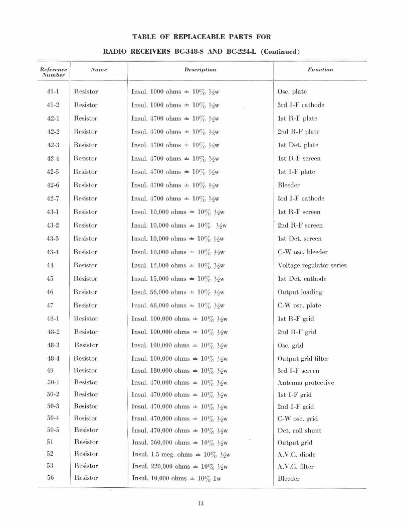
TABLE OF REPLACEABLE PARTS FOR
RADIO RECEIVERS BC.348-S AND BC-224-L (Continued)
Reference Name Descr iption F,inction Nu ,n ber
41-1 Hesistor Insul. 1000 ohms ± 10% Yzw Osc. plate
41-2 Hesistor Insul. 1000 ohms ± 10% Yzw 3rd 1-F cathode
42-1 Resistor Insul. 4700 ohms ± 10% Yzw 1st R-F plate
42-2 Resistor Insul. Lt700 ohms ± 10% Yzw 2nd R-F plate
42-3 Resistor Insul. 4700 ohms ± 10% Yzw 1st Det. plate
42-4 Hesistor Insul. 4700 ohms ± 10% Yzw 1st H-F screen
42-5 Hesistor Insul. 4700 ohms ± 10% Yzw 1st 1-F plate
42-6 Resistor Insul. 4700 ohms ± 10% Yzw Bleeder
42-7 Resistor Insul. 4700 ohms ± 10% Yzw 3rd 1-F cathode
43-1 Resistor Insul. 10,000 ohms ± 10% Yzw 1st H-F screen
43-2 Resistor lnsul. 10,000 ohms ± 10% Yzw 2nd H-F screen
43-3 Resistor lnsul. 10,000 ohms ± 10% Yzw 1st Det. screen
43-4 Resistor lnsul. 10,000 ohms ± 10% Yzw C-W osc. bleeder
44 Resistor lnsul. 12,000 ohms ± 10% Yzw Voltage regulator series
45 Resistor lnsul. 15,000 ohms ± 10% Yzw 1st Det. cathode
46 Resistor lnsul. 56,000 ohms ± 10% Yzw Output loading
47 Resistor lnsul. 68,000 ohms ± 10% Yzw C-W osc. plate
48-1 Hesistor lnsul. 100,000 ohms ± 10% Yzw 1st R -F grid
48-2 Resistor lnsul. 100,000 ohms ± 10% Yzw 2nd H-F grid
48-3 Resistor lnsul. 100,000 ohms ± 10% Yzw Osc. grid
48-4 Resistor lnsul. 100,000 ohms ± 10% Yzw Output grid filter
49 Hesistor Insul. 180,000 ohms ± 10% Yzw 3rd I-F screen
50-1 Resistor lnsul. 470,000 ohms ± 10% Yzw Antenna protective
50-2 Hesistor Insul. 470,000 ohms ± 10% Yzw 1st 1-F grid
50-3 Hesistor lnsul. 470,000 ohms ± 10% Yzw 2nd 1-F grid
50-4 Hesistor lnsul. 470,000 ohms ± 10% Yzw C-W osc. grid
50-5 Resistor lnsul. 470,000 ohms ± 10% Yzw Det. coil shunt
51 Resistor lnsul. 560,000 ohms ± 10% Yzw Output grid
52 Resistor lnsul. 1.5 meg. ohms ± 10% Yzw A.V.C. diode
53 Resistor lnsul. 220,000 ohms ± 10% Yzw A.V.C. filter
56 Resistor lnsul. 10,000 ohms ± 10% 1 w Bleeder
13

TABLE OF REPLACEABLE PARTS FOR
RADIO RECEIVERS BC-348-S AND BC-224-L (Continued)
Reference Name Description Function Numbe r
-----
57 Resistor Insul. 27,000 ohms ± 10% lw Voltage regulator
58 Resistor Variable 3500 ± 10% to 10 ohms .1 watt Noise compensator
59-A Resistor Volume control. front unit 20,000 ohms ± 10% M. V.C. to 10 ohms 2 watt
59-B Resistor Volume control back unit 350,000 ohms ± 10% A. V. C. to 50 ohms .2 watt
61 Resistor Insul. 2400 ohms ± 5% Yzw Output plate
62 Resistor Insul. 47,000 ohms ± 10% Yzw Bleeder
64 Capacitor Ceramic 500 volts 35 mmf ± 5% with leads Osc. temp. compensating
65 Capacitor Air trimmer 10 mmf max. Ant. trimmer
66 Capacitor Ceramic trimmer 25 mmf working Osc. series padder
67 Capacitor Mica 500 volts d-c 750 mmf ± 5% with leads R-F plate tuning
68 Capacitor Molded paper .1 mfd. ± 10% 4,00 volts 2nd I-F cathode by-pass
71 Inductance Antenna band 1 1st R-F tuned circuit
72 Inductance Antenna band 2 1st R-F tuned circuit
73 Inductance Antenna band 3 1st R-F tuned circuit
74 Inductance Antenna band 4 1st R-F tuned circuit
75 Inductance Antenna band 5 1st R-F tuned circuit
76 Inductance Antenna band 6 1st R-F tuned circuit
77 Inductance R-F band 1 1st R-F to 2nd R-F coupling
78 Transformer R-F band 2 1st R-F to 2nd R-F coupling
79 Transformer R-F band 3 1st R-F to 2nd R-F coo .ling
80 Transformer R-F band 4 1st R-F to 2nd R -F coupling
81 Transformer R-F band 5 1st R-F to 2nd R-F coupling
82 Transformer R-F band 6 1st R-F to 2nd R-F coupling
83 Transformer 1st det. band 1 2nd R-F to det. coupling
84 Transformer 1st det. band 2 2nd R-F to det. coupling
85 Transformer 1st det. band 3 2nd R-F to det. coupling
86 Transformer 1st det. band 4 2nd R-F to det. coupling
87 Transformer 1st det. band 5 2nd R-F to det. coupling
88 Transformer 1st det. band 6 2nd R-F to det. coupling
14

TABLE OF REPLACEABLE PARTS FOR
RADIO RECEIVERS BC-348-S AND BC-224-L (Continued)
Reference Nan1,e Description Fltnction Niirn ber
89 Transformer Osc. band 1 Osc. to 1st det. coupling
90 Transformer Osc. band 2 Osc. to 1st det. coupling
91 Transformer Osc. band 3 Osc. to 1st det. coupling
92 Transformer Osc. band 4 Osc. to 1st det. coupling
93 Transformer Osc. band 5 Osc. to 1st det. coupling
94 Transformer Osc. band 6 Osc. to 1st det. coupling
95 Transformer 1st I-F 1st Det. to crystal coupling
96 Transformer Crystal filter Crystal to 1st I-F coupling
97 Transformer 2nd I-F 1st I-F to 2nd I-F coupling
98 Transformer C-W osc. Grid & plate coupling
99 Transformer 3rd I-F 2nd I-F to 3rd I-F coupling
100 Transformer 4th I-F 3rd I-F to 2nd det. coupling
101-A Transformer Audio Output
101-B Choke Audio frequency Filter
101-C Capacitor Paper 400 volts d-c .05 mf ± 10% C-W osc. time constant
102-1 Jack Single circuit Headphone
102-2 Jack Single circuit Headphone
103 Regulator Neon bulb type 991 Osc. plate voltage regulator
104 Lamp 6 to 8 volts type 44 Dial light
105 Switch SPST type Crystal filter (out-in)
106 Switch DPST type C-W osc. (on-off)
107 Switch 3 position, 2 wafer A. V. C. Off M. V. C.
108 Switch 6 position, 1 wafer Band switch, antenna unit
109 Switch 6 position, 1 wafer Band switch, antenna unit
110 Switch 6 position, 1 wa.f er Band switch, H-F unit
111 Switch 6 position, 1 wafer Band switch, H-F unit
112 Switch 6 position, 1 wafer Band switch, det. unit
113 Switch 6 position, 1 wafer Band switch, det. unit
114 Switch 6 position, 1 wafer Band switch, osc. unit
115 Switch 6 position, 1 wafer Band switch, osc. unit
15

-TABLE OF REPLACEABLE PARTS FOR
RADIO RECEIVERS BC-348-S AND BC-224-L (Continued)
Reference 1Ya,ne Description Function Ntunber
116 Switch 6 position, 1 wafer Band switch, osc. unit
117 Switch 6 position, 1 wafer Band switch, osc. unit
121 · Crystal assembly 915 kc crystal mounted in case I-F filter
251 1st I-F trans-former assembly
Complete with shield can 1st det. to 1st I-F coupling
252 2nd I-F trans-former assembly
Complete with shield can 1st I-F to 2nd I-F coupling
253 3rd I -F trans-former assembly
Complete with shield can 2nd I-F to 3rd I-F coupling
254 4th I-F trans-former assembly
Complete with shield can 3rd I-F to 2nd det. coupling
255 Crystal filter Complete wit h shield can I-F selectivity assembly
256 C-W osc. Complete with shield can C-W rei eption assembly
301 Choke R-F Dynamotor filter
302 Choke R-F Dynamotor filter
303-A Capacitor Paper 250 volts d-c .5 mf ± 20% Dynamotor filter
303-B Capacitor Paper 250 volts d-c .5 mf ± 20% Dynamotor filter
304-1 Capacitor iica 500 volts d-c .Ol mf ± 10% Dynamotor filter
304-2 Capacitor Mica 500 volts d-c .01 mf ± 10% Dynamotor filter
305 Capacitor Paper 400 volts d-c 1.0 mf ± 20% Dynamotor filter
*500 Resistor Variable 200 ohms ± 10% 4 watts Dial lamp control
*501-A Resistor Insulated 3 ohms + 10% - 50% 1.5 watts Filament
*501-B Resistor Insulated 190 ohms + 10% - 15% 1.9 watts Filament
*502 Fuse 5-Amp 25-volt Type Primary protective
*503 Resistor Insulated 60 ohms ± 10% 3.7 watts Dial lamps series
*510 Dynamotor 28 Volts 1.23 amp, 220 volts .070 amp, 44,00 rpm. Motor generator
PARTS USED ONLY IN BC-224-L
54 Resistor Insul. 0.5 ohms ± 10% 1 watt Filament
55 Resistor Insul. 68 ohms ± 10% 1 watt Filament balance
60 Resistor Variable, 75 ohms ± 10% Dial lamp control
118 Fuse FU-23 10-Amp. 25-volt Primary protective
300 Dynamotor 13.8 volts, 2.45 amp; 220 volt, .07 amp; 4400 Motor generator r .p.m.
*Receiver BC-348-S only.
16
l
~ --------7,{------
~ -
aB.curouT INOl( iU[Sto
0AiNQ VL ,. ,.(ONOI.NT
f !l fUIQ, A,,LICA&l.t HI TIIIUf ~SITIONS l'L •QI0.) (1 U •,., . <1 0 4)
rio,A HOLl (CO.DVlf u ; ... os ODWff) fol\n,.'f1C...,.l1Pf ,,.TT. Ci ON .. 'f ,,...,,o, ~"'" · 4 0 ))
J--f--------------- fl CUl Ov T ----------...,
_._,.___ _t_ --·-'"'~ I I
~
______ ]=a
FIGURE 6-RADIO RECEIVER BC-348-S, DRILLING PLAN
L'- .42. 0
MOUNTir-tG --:[:;:t·;1: ··:ty-r:-
9 .&01
: '-1" : I
ll!t. O lw'IAA .
rh RE AR Y1 1t w 'r ! CONNOCTOe.
w
BorToM V1 Ew
WtT~OUT MoUl"l'T"1NG 8AS~
·~::':\~\:::::~-.-M-A_< ____ O~-~~n,o::~
~rMAK .
~ J __ ~-~·
"'---.., 0\JNTIN6 SI DE. v,~w
FIGURE 7-RADIO RECEIVER BC-348-S, O UTLINE DIMENSIONAL SKETCH
17

>-:rj
2i e :,:, M co I
!:t1 > t::,
0 !:t1 M (") M
< M :,:,
...... t,j 'D ('")
w ,i::. co ~(fl (fl (")
~ M s::: > ..., ;::; Si' > " :,:, > ;;::
119 ANT,
" "' J 120
CND_
OYNAMOTOR POWCR SUPPLY
JOI
JOZ
++ ZBV.
~
~l
12-1
OUT· - -~tJT 28 V.
VT· 86. 2RF
: v: ,.L ,;, •
VT-91 1 OET. ~
I I I I ____________ _J
56 I 4Z-f>
~ ...
<t ,t I VOlTA<;C ,.... RC(iULATOR
"'
"61 .. z
Rf:LAY
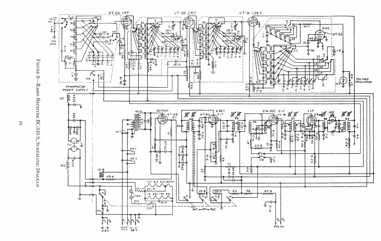
~ ~
~ Cj ~ 1:%:l
00
I ~ > t:, -0
~ 1:%:l Ci 1:%:l -< 1:%:l ~
I--' bj \0 (j
I
C),j if::.. 00
I
'CJ)
'CJ) Ci ~ 1:%:l
~ > t-3 ~
Ci
t::; -> ~ ~ > ~
I
~
120 C N D_
-. ~I I -L ____ -:- -- ·
108
OYNAMOTOR POWCR SUPPLY
301
302
~ i I I I I I
- _J
++ Z.8 v.
12-1
OUT· - -'!"'UT 28V.
VT- 86. 2 R.F. r ----- - - -- -- ---,
1"1' ..... ~ () -+---.__ ....... _
I) N
ID ...,
11 f. 2.~f. 3 Lf. OUTPUT
I I I I ., I I I I I I I I I I I I 1, : I
I I
!
VT-91 1 OET.
I - I
I I ____________ _J
:!? I
en
53
N 11'1
':
~
~ VOLTAGE: ,._ RC(iUI.ATOR
"'
I
C7'I
RELAY

IZ
WVll~VIQ :HJ.VW,IH:::>S '1-i,zz-Ja lI3:AI3::::>3'lJ OICTVU-6 :rnn~I.f
2 304- i
,1; ·1 304r;I
is+~ <-t
~~ :-· I : - ~ I . ~: ~· . , dQ.4 . I 1 , r , r i) I i
:D p oil
~~
•lh 9 - 13 1
. !
4 2·4
42 · 3
"' ~
305
;go ~-<
"-~:?: ,11~
gj; J 10-1
~ :,11HI ,u••r •00 l•"l •00 l• oo::J ~·1 I, 1!:d I :jl:n I
~ :
< 7 O>
"' N :D
"'
< -! I
U)
,-.---, , 't1ill1Jl 5
:D< 80 c~ r ~ ~..., 0 :D
..., -!
< 7 "' (ft
~

N> I-'
I
:x
120 GND.
~ ~
~ c::: ::0 M
\0
I ~ > i:::::, ~
0
~ M {j
M ~
<: M ::0
to (j
I
1:-v t.....:) If:..
I r ~
r:..n {j
~ M ~ > t-3 ~
{j
0 ~
> ~ ::0 > ~
VT-86 lRF. ,---2 ------ - ----- -- ---7
C\I I
~
I ~ I ~I 108 L _____ -= ----
DYNAMOTOR POWER SUPPLY
301
I CD •
101-B
II
+ -t-14 V
I
12-1
!02-1
102-2
54
,.._ - - --
OUT· - -PUT 14V
I O>
~
ci a: ,.,
tw 0
i-: ~
m ~ CD I")
V -48 OUTPUT
VT-86 2RF.
.....
~ Ci z C\I
0 z C\I
IL -· I-' ~
I-::::, a. I-::::, 0
-:-- T O> ...,
0
C\I
'°
I..,,_,___ __
..k ..._ _____ __,,
u ' ' ' Ill -·. - - - - 10,- - - - ....._ -- -O AVC- OFF-Mvc-=--
53
VT-91 1DET.
/ /
/ /
/ /
VT-65 OSC. ,,,-- - - - - - - - - -,
/ '° I / =
.__.~----+---+-+-+-+4~~ ...... __. I I I IJ03
-C\I st,., ,:-t otl'° I "= I -ID l")I '° 1 chrli I I! !..!.-~ - - - - - - '/ii_ - - ":.. - ~ - - - - - - - - - J
VT-70 C.W. OSC. 2 I.F.'
RELAY
VT-86 1 I.F
., • VOLTAGE
REGULATOR !;=;