instituto de computaÇÃoreltech/2015/15-01.pdf · instituto de computaÇÃo ... linear delay...
TRANSCRIPT
�������������������� ��������������������������������������������������������������������������������������������INSTITUTO DE COMPUTAÇÃOUNIVERSIDADE ESTADUAL DE CAMPINAS
FDPE (Fast and Accurate Dynamic Power
Estimation): Implementation and User
Guidelines
D. Vidal M. L. Côrtes
Technical Report - IC-15-01 - Relatório Técnico
February - 2015 - Fevereiro
The contents of this report are the sole responsibility of the authors.
O conteúdo do presente relatório é de única responsabilidade dos autores.
FDPE (Fast and Accurate Dynamic Power Estimation):
Implementation and User Guidelines
Daniel Vidal Mario Lucio Cortes
Abstract
This Technical Report presents the implementation details and usage guidelines ofFDPE framework. FDPE provides fast and accurate dynamic power estimation forgate-level digital circuits using Liberty characterization data and Verilog simulator.
This framework enables accurate power estimation and achieves a speed-up of threeorders of magnitude over Spice. FDPE also enables dynamic power estimation for largescale circuits that are unfeasible to run in Spice simulations. In addition, FDPE hasthe following advantages over similar tools: ease of use, flexibility, low-cost, and publicavailability.
Contents
1 Introduction 2
2 Logic cells data formats and modeling technology 2
3 Power model design and description 7
4 FDPE implementation 11
5 Usage and known limitations 17
6 Conclusions 19
References 20
1

1 Introduction
Analog simulation with tools such as Spice has been used for decades in integrated circuitsto accurately estimate current and voltage signals, including dynamic power. However,due to its intrinsic computational complexity, it is unfeasible to run Spice simulations inmedium to large circuits. Another simulation approach Fast-Spice [1] was developed, usingsimplified transistor models and alternative numerical solution methods, resulting in fastersimulation at the cost of lower accuracy.
The use of higher level circuit models may produce simulation speed-ups even betterthan the one achieved with Fast-Spice. One typical high-level circuit model is known asgate-level. A gate-level circuit representation describes a circuit as basic logic cells (AND,OR, NAND, etc.) and allows the use of efficient event-driven logic simulation.
This technical report presents the implementation details of a novel framework, namedas FDPE [2], which models the dynamic power behavior of digital systems in gate-levelsimulations and has the following attributes:
� Accuracy: as compared to Spice and existing solutions;
� Speed: three orders of magnitude speed-up with respect to sign-off quality Spice sim-ulation;
� Ease of use: can be easily integrated to the existing design flows; uses standard Libertyformat [3] for describing the cells; does not require individual cell characterization;
� Flexibility and low-cost: can use any logic simulator, including open source solutions,as long as it is compatible to Verilog and VPI [4];
� Public availability: as opposed to other published solutions, our proposal is fullyavailable for public use.
In order to build the dynamic power behavior, a power model is added to the typical behav-ioral cell model, and physical characteristics (energy and timing) are taken into account.
The report is organized as follows: Section 2 contains a brief explanation about logiccells data formats and modeling technology used by FDPE, Section 3 describes the powermodel used in FDPE, Section 4 presents the implementation of power model in FDPEframework, Section 5 presents the framework usage guidelines and known limitations, andSection 6 presents conclusions.
2 Logic cells data formats and modeling technology
2.1 Liberty library and characterization data of logic cells
Liberty is an open source gate-level modeling technology, widely accepted by standard celllibrary vendors and/or foundries, and EDA software. It contains the needed informationfor circuit implementation such as area, timing (propagation delays and transition times),and power. This section briefly introduces Liberty capabilities that are relevant for FDPE.
2
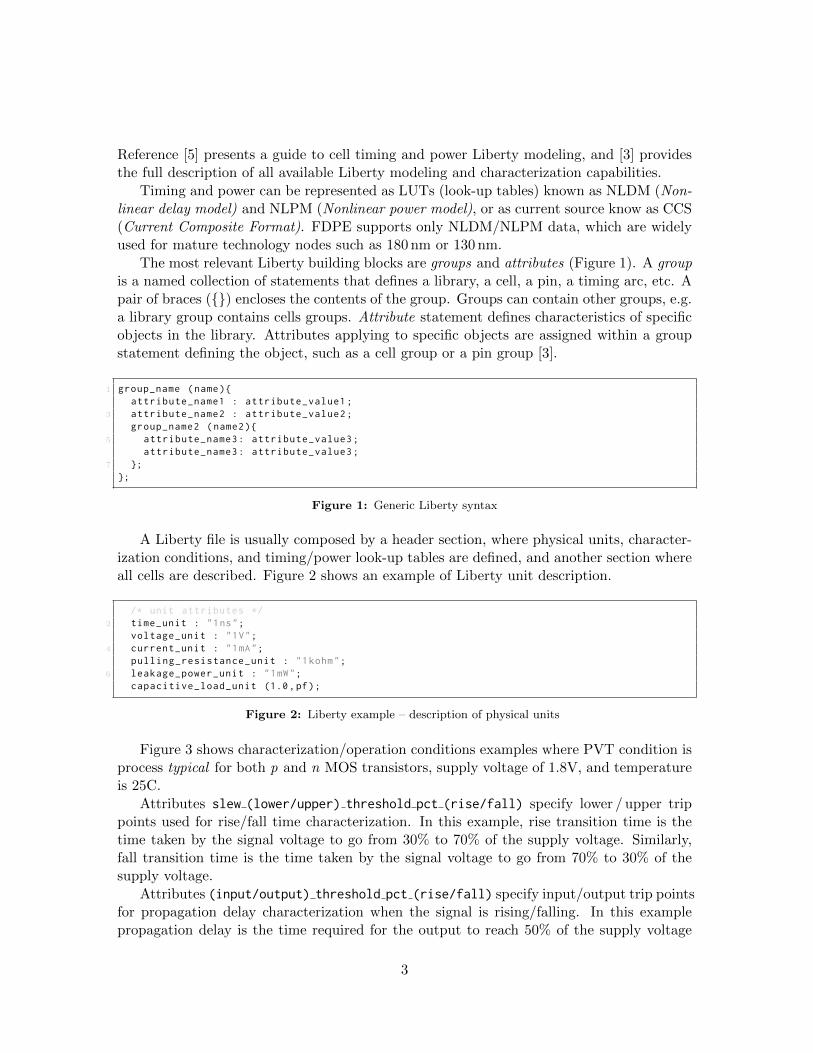
Reference [5] presents a guide to cell timing and power Liberty modeling, and [3] providesthe full description of all available Liberty modeling and characterization capabilities.
Timing and power can be represented as LUTs (look-up tables) known as NLDM (Non-linear delay model) and NLPM (Nonlinear power model), or as current source know as CCS(Current Composite Format). FDPE supports only NLDM/NLPM data, which are widelyused for mature technology nodes such as 180 nm or 130 nm.
The most relevant Liberty building blocks are groups and attributes (Figure 1). A groupis a named collection of statements that defines a library, a cell, a pin, a timing arc, etc. Apair of braces ({}) encloses the contents of the group. Groups can contain other groups, e.g.a library group contains cells groups. Attribute statement defines characteristics of specificobjects in the library. Attributes applying to specific objects are assigned within a groupstatement defining the object, such as a cell group or a pin group [3].
1 group_name (name){attribute_name1 : attribute_value1;
3 attribute_name2 : attribute_value2;group_name2 (name2){
5 attribute_name3: attribute_value3;attribute_name3: attribute_value3;
7 };};
Figure 1: Generic Liberty syntax
A Liberty file is usually composed by a header section, where physical units, character-ization conditions, and timing/power look-up tables are defined, and another section whereall cells are described. Figure 2 shows an example of Liberty unit description.
/* unit attributes */2 time_unit : "1ns";
voltage_unit : "1V";4 current_unit : "1mA";
pulling_resistance_unit : "1kohm";6 leakage_power_unit : "1mW";
capacitive_load_unit (1.0,pf);
Figure 2: Liberty example – description of physical units
Figure 3 shows characterization/operation conditions examples where PVT condition isprocess typical for both p and n MOS transistors, supply voltage of 1.8V, and temperatureis 25C.
Attributes slew (lower/upper) threshold pct (rise/fall) specify lower / upper trippoints used for rise/fall time characterization. In this example, rise transition time is thetime taken by the signal voltage to go from 30% to 70% of the supply voltage. Similarly,fall transition time is the time taken by the signal voltage to go from 70% to 30% of thesupply voltage.
Attributes (input/output) threshold pct (rise/fall) specify input/output trip pointsfor propagation delay characterization when the signal is rising/falling. In this examplepropagation delay is the time required for the output to reach 50% of the supply voltage
3

when the input changes to 50% of the supply voltage.Attribute slew derate factor specifies how the transition times recorded in the library
need to be derated to match the measured transition times. In this example all transitiontimes are measured as 30%↔ 70% of the supply voltage and represented as 10%↔ 90% ofthe supply voltage. The scaling is calculated as:
slew derate factor =tmeasuredtrepresented
=⇒ slew derate factor =t30%↔70%
t10%↔90%≡ 0.7− 0.3
0.9− 0.1
In NLDM modeling, any physical parameter y (e.g. output transition time, propagationdelay, power) is modeled as a function of multiple input variables x1, x2, . . . , xn (e.g. inputtransition times, output capacitance). Each modeled parameter is represented in Libertyfile as an n dimension table.
In order to build the tables, many combinations of x1, x2, . . . , xn inputs are simulatedand for each simulated combination, y is measured and recorded in a table.
Figure 4 shows NLDM/NLPM table definitions. Both tables in example are 2D, whereone index is the input transition time and the other index is total output capacitance. Inthis section, the index values are meaningless and are used only as placeholders to specifythe table dimension, which is 7× 7 in this case.
Figure 5 shows an inverter cell definition as an example of Liberty cell descriptionsection. In timing and power modeling groups, output pins usually have a related pinwhich specify the input pin reference, e.g. a AND cell may have many similar timing andpower groups: one for each input related pin.
1 /* operation conditions */nom_process : 1;
3 nom_temperature : 25;nom_voltage : 1.8;
5 operating_conditions(tt) {process : 1;
7 temperature : 25;voltage : 1.8;
9 tree_type : balanced_tree;}
11 default_operating_conditions : tt;
13 /* threshold definitions */slew_lower_threshold_pct_fall : 30.0; slew_upper_threshold_pct_fall : 70.0;
15 slew_lower_threshold_pct_rise : 30.0; slew_upper_threshold_pct_rise : 70.0;input_threshold_pct_fall : 50.0 ; output_threshold_pct_fall : 50.0;
17 input_threshold_pct_rise : 50.0 ; output_threshold_pct_rise : 50.0;slew_derate_from_library : 0.5 ;
Figure 3: Liberty example – description of characterization conditions
4

1 lu_table_template(delay_template_7x7) {variable_1 : input_net_transition;
3 variable_2 : total_output_net_capacitance;index_1 ("1000, 1001, 1002, 1003, 1004, 1005, 1006");
5 index_2 ("1000, 1001, 1002, 1003, 1004, 1005, 1006");}
7 power_lut_template(energy_template_7x7) {variable_1 : input_transition_time;
9 variable_2 : total_output_net_capacitance;index_1 ("1000, 1001, 1002, 1003, 1004, 1005, 1006");
11 index_2 ("1000, 1001, 1002, 1003, 1004, 1005, 1006");}
Figure 4: Liberty example – description of NLDM/NLPM tables
1 cell (INVX1L) {area : 6.585600;
3 pin(Y) {direction : output;
5 capacitance : 0.0;function : "(!A)";
7 internal_power () {related_pin : "A";
9 rise_power(energy_template_7x7) {index_1 ("0.040000 , 0.080000 , 0.158000 , 0.318000 , 0.638000 , 1.280000 , 2.570000");
11 index_2 ("0.000500 , 0.001475 , 0.004351 , 0.012837 , 0.037871 , 0.111722 , 0.329590");values ( \
13 "0.009863 , 0.009935 , 0.010058 , 0.010426 , 0.011575 , 0.014093 , 0.020857", \"0.010466 , 0.010421 , 0.010275 , 0.010551 , 0.011397 , 0.013713 , 0.020707", \
15 "0.011892 , 0.011927 , 0.012080 , 0.011195 , 0.011463 , 0.012660 , 0.019826", \"0.015458 , 0.015221 , 0.014154 , 0.012779 , 0.012949 , 0.013447 , 0.020182", \
17 "0.022368 , 0.022121 , 0.021192 , 0.019504 , 0.017239 , 0.009529 , 0.011902", \"0.037524 , 0.036958 , 0.035722 , 0.032299 , 0.029018 , 0.023659 , 0.024747", \
19 "0.069801 , 0.069726 , 0.069057 , 0.059942 , 0.055479 , 0.046033 , 0.039835");fall_power(energy_template_7x7) {index_1 (...); index_2 (...); values (...);}
21 }timing () {
23 related_pin : "A";timing_sense : negative_unate;
25 cell_rise(delay_template_7x7) {index_1 (...); index_2 (...); values (...);}
27 rise_transition(delay_template_7x7) {index_1 (...); index_2 (...); values (...);}
29 cell_fall(delay_template_7x7) {index_1 (...); index_2 (...); values (...);}
31 fall_transition(delay_template_7x7) {index_1 (...); index_2 (...); values (...);}
33 }max_capacitance : 0.329590;
35 }pin(A) {
37 direction : input;capacitance : 0.003324;
39 }cell_leakage_power : 0.000000024258;
41 }
Figure 5: Liberty example – inverter cell
5

2.2 Verilog cell behavioral modeling
Verilog is a hardware description language widely used in industry for description, simula-tion, and synthesis of digital systems in many abstraction levels. The abstraction level ofinterest in FDPE is named gate-level, where the system is represented by cells of a stan-dard logic cell library. This section presents a brief introduction to Verilog cell modeling.Detailed explanations and examples can be found in [6], and a full description of Verilogcapabilities can be found in [4].
In order to simulate a circuit mapped to a standard cell library, each used cell must havea behavioral model. A Verilog cell model is usually built using 3 basic functions: built-inprimitives, user defined primitives, and timing description.
Verilog has built-in gates and transmission gates primitives that can be used to describebasic logic functionality or to build complex logic functions (Figure 6 and Table 1). Complexlogic functions (e.g. full-adders, and-or cells, muxes) and memory elements (e.g. latches andflip-flops) are usually described by user defined primitives that are primitive logic functionsdescribed by logic tables.
Timing description is a group of expressions that defines logic paths and their timingvalues, and timing checks (e.g. setup, hold, minimum pulse). Figure 7 shows a typicalexample of an inverter cell Verilog model.
nor
or and
nand xnor
xorbuf
inv
bufif1
notif1
bufif0
notif0
Figure 6: Verilog built-in gates and transmission gates primitives
Table 1: Description of Verilog built-in primitives
gate description gate description
and N-input AND gate not N-output inverter
nand N-input NAND gate buf N-output buffer
or N-input OR gate bufif0 Tri-state buffer, active low enable
nor N-input NOR gate bufif1 Tri-state buffer, active high enable
xor N-input XOR gate notif0 Tri-state inverter, active low enable
xnor N-input XNOR gate notif1 Tri-state inverter, active high enable
6

module INVX1L ( Y, A );2 output Y;
input A;4
//gate primitive6 not I0 (Y , A);
8 // timing sectionspecify
10 // delay parametersspecparam
12 tplh$A$Y = 1,tphl$A$Y = 1;
14 // path delays(A *> Y) = (tplh$A$Y , tphl$A$Y);
16 endspecifyendmodule
Figure 7: Typical Verilog model for an inverter cell
3 Power model design and description
FDPE power model design decisions and rationale are described as follows:
� Isosceles Triangular power model aiming at accuracy and efficiency. Triangular shapeis close to CMOS gates real current waveform [7] and it can be represented efficientlyin an event driven simulator [8]. A more accurate model is an asymmetrical triangleshape as used in [8] and [9]. Nevertheless, FDPE approach uses a simpler model thatachieves reasonable accuracy.
� Power estimation at simulation time, like in [10, 8]. This feature provides ease of useand flexibility, since post simulation processing and circuit activity database are notrequired.
� Liberty format based as in [9]. This is a widely used format, usually supplied bystandard cell library vendors and foundries. It contains all necessary data for transientpower estimation, namely timing and energy. This feature provides ease of use as noadditional cell characterization is needed.
� Verilog based. It is a standard hardware description language and it provides aninterface mechanism (VPI) that allows read/write access to internal structures ofthe circuit [4]. VPI enables communication between models and Liberty data. Thisfeature provides flexibility and low-cost, as the workflow is similar to typical gatelevel simulations and any Verilog simulator that supports VPI can be used, includingfreeware simulators.
� Leakage neglected. In modern deep sub-micron CMOS technology leakage power can-not be neglected as it is a significant component of overall power and also can exhibitdynamic behavior. However, this simplification is acceptable for mature technologynodes such as 180nm, which are still widely used.
The following subsections present the FDPE power model design.
7
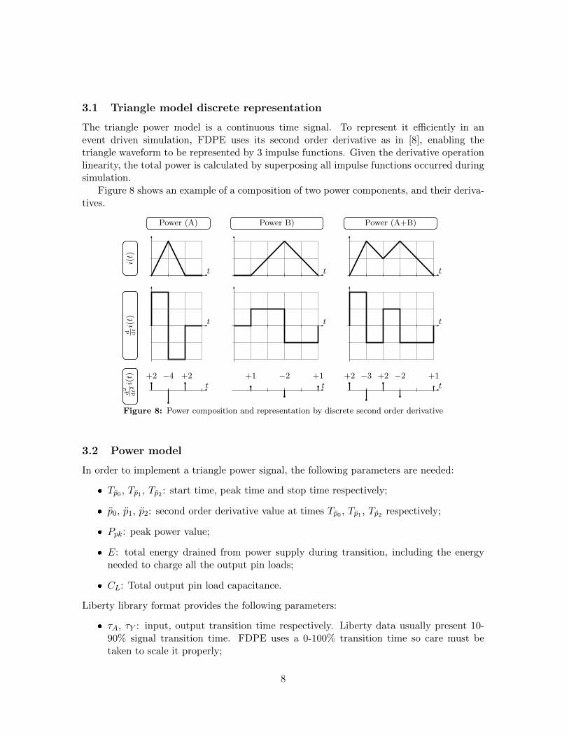
3.1 Triangle model discrete representation
The triangle power model is a continuous time signal. To represent it efficiently in anevent driven simulation, FDPE uses its second order derivative as in [8], enabling thetriangle waveform to be represented by 3 impulse functions. Given the derivative operationlinearity, the total power is calculated by superposing all impulse functions occurred duringsimulation.
Figure 8 shows an example of a composition of two power components, and their deriva-tives.
i(t)
+2
d dti(t)
t t t
ttt
t
Power (A) Power B) Power (A+B)
+2−4
d2
dt2i(t) +1 −2 +1 +2 −3 +2 −2 +1
t t
Figure 8: Power composition and representation by discrete second order derivative
3.2 Power model
In order to implement a triangle power signal, the following parameters are needed:
� Tp0 , Tp1 , Tp2 : start time, peak time and stop time respectively;
� p0, p1, p2: second order derivative value at times Tp0 , Tp1 , Tp2 respectively;
� Ppk: peak power value;
� E: total energy drained from power supply during transition, including the energyneeded to charge all the output pin loads;
� CL: Total output pin load capacitance.
Liberty library format provides the following parameters:
� τA, τY : input, output transition time respectively. Liberty data usually present 10-90% signal transition time. FDPE uses a 0-100% transition time so care must betaken to scale it properly;
8
� tpd: input to output propagation delay;
� EINT : energy drained from power supply during transition, considering only MOSshort circuit current and energy required to charge internal nodes;
� CA: input pin capacitance.
In addition, the event time of an input transition, TA is needed to trigger the power model.
The implemented power model follows an intuitive approach, which can be considereda simplified version of [9]. FDPE power models were developed for two categories of cells:combinational and sequential which are presented as follows.
3.2.1 Combinational model
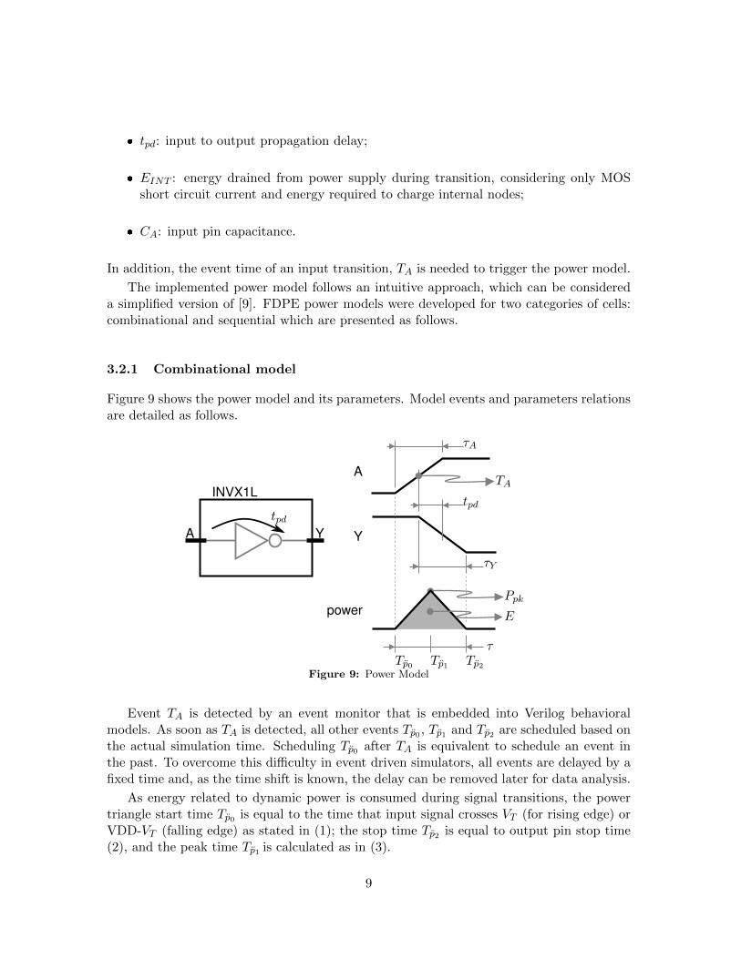
Figure 9 shows the power model and its parameters. Model events and parameters relationsare detailed as follows.
Ppk
τY
τA
tpd
A
power
INVX1L
tpdA Y Y
TA
E
τTp0 Tp1 Tp2
Figure 9: Power Model
Event TA is detected by an event monitor that is embedded into Verilog behavioralmodels. As soon as TA is detected, all other events Tp0 , Tp1 and Tp2 are scheduled based onthe actual simulation time. Scheduling Tp0 after TA is equivalent to schedule an event inthe past. To overcome this difficulty in event driven simulators, all events are delayed by afixed time and, as the time shift is known, the delay can be removed later for data analysis.
As energy related to dynamic power is consumed during signal transitions, the powertriangle start time Tp0 is equal to the time that input signal crosses VT (for rising edge) orVDD-VT (falling edge) as stated in (1); the stop time Tp2 is equal to output pin stop time(2), and the peak time Tp1 is calculated as in (3).
9

Tp0 = TA − (τA/2)× V DD − VTV DD
(1)
Tp2 = TA + tpd + (τY/2) (2)
Tp1 = (Tp0+Tp2)/2 (3)
In case an input transition does not cause an output toggle, e.g. a transition at one inputof an AND cell with the other input at zero, the stop time is considered to be the inputslope stop time (4).
Tp2 = TA + (τA/2) (4)
The energy drained from power supply is equal to the area of its power signal waveform[7]. By geometry, Ppk can be calculated as in (5).
E =Ppk × τ
2=⇒ Ppk =
2× Eτ
(5)
If an input signal transition does not cause an output toggle, or it causes a high to lowtransition on cell output, total energy is equal to internal energy only (6).
E = EINT (6)
If an input signal transition causes an output transition from low to high, total energyis equal to internal energy plus the energy needed to charge the total load capacitance (7).
E = EINT + EL (7)
EL =V 2DD × CL
2(8)
Load capacitance CL of an output pin is computed as the sum of input capacitance CAof all inputs connected to that output net. Second order derivatives p0, p1,p2 are calculatedbased on triangle geometry and symmetry:
p0 =Ppkτ/2
(9)
p1 = −2p0 (10)
p2 = p0 (11)
3.2.2 Sequential model
The power model for sequential cells is built similarly to combinational cells: the trianglestart, peak and stop times are determined by signal transition time. However, in this casethere is one power model for each pin as each pin has its own related energy information inLiberty data. Each pin type is explained as follows.
10

Clock Start time is considered to be as in equation (1) and stop time is considered to beas in equation (12), according to [9]. TCK is the clock pin transition time, tCK→Qis theclock to output delay and τQ is output transition time.
Tp2 = TCK + tCK→Q − (τQ/2) (12)
Data Input Start, stop and peak time are assumed to be similar to the combinationalcell, when the input does not cause an output transition, as stated in equations (1), (4),and (3).
Data output Start and stop time are considered to match the transition start and end,and are calculated as in equations (13) and (14).
Tp0 = TQ − (τQ/2) (13)
Tp2 = TQ + (τQ/2) (14)
The internal energy related to data output pin, EINTQ , stored in Liberty includes the energyrelated to clock pin, EINTCK
. Therefore, it is necessary to subtract EINTCKfrom EINTQ in
order to calculate the energy considered to build the triangle model as shown in equation(15) for rising transition, and as in equation (16) for falling transition.
E = EINTQ − EINTCK+ EL (15)
E = EINTQ − EINTCK(16)
4 FDPE implementation
4.1 Verilog model modifications
In order to include the power model of section 3, Verilog cell models had to be modified. Theparameters stated in section 3.2.1 were implemented as Verilog variables, mapped accordingto Table 2. Additionally, two Verilog variables and two Verilog parameters were needed fortransition annotation (Section 4.2.1):
� n in : total number of input pins;
� t count : number of input pins that had transition times annotated;
� t ready : output pin transition time annotated (1: annotated, 0: not annotated)
� <pin> sense : signal propagation unateness1 relation between output and input<pin> (1: positive unate, -1:negative unate, 0: non-unate)
11
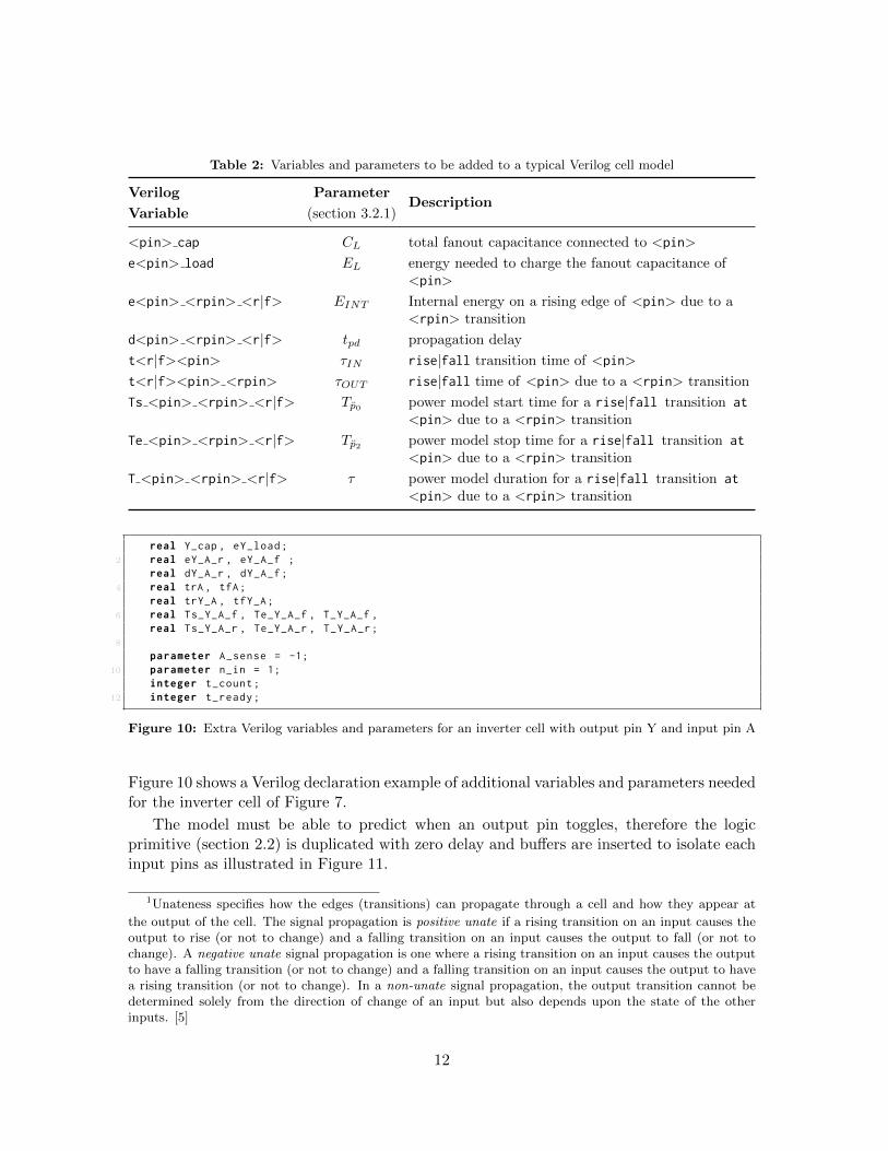
Table 2: Variables and parameters to be added to a typical Verilog cell model
Verilog ParameterDescription
Variable (section 3.2.1)
<pin> cap CL total fanout capacitance connected to <pin>
e<pin> load EL energy needed to charge the fanout capacitance of<pin>
e<pin> <rpin> <r|f> EINT Internal energy on a rising edge of <pin> due to a<rpin> transition
d<pin> <rpin> <r|f> tpd propagation delay
t<r|f><pin> τIN rise|fall transition time of <pin>
t<r|f><pin> <rpin> τOUT rise|fall time of <pin> due to a <rpin> transition
Ts <pin> <rpin> <r|f> Tp0power model start time for a rise|fall transition at<pin> due to a <rpin> transition
Te <pin> <rpin> <r|f> Tp2power model stop time for a rise|fall transition at<pin> due to a <rpin> transition
T <pin> <rpin> <r|f> τ power model duration for a rise|fall transition at<pin> due to a <rpin> transition
real Y_cap , eY_load;2 real eY_A_r , eY_A_f ;
real dY_A_r , dY_A_f;4 real trA , tfA;
real trY_A , tfY_A;6 real Ts_Y_A_f , Te_Y_A_f , T_Y_A_f ,
real Ts_Y_A_r , Te_Y_A_r , T_Y_A_r;8
parameter A_sense = -1;10 parameter n_in = 1;
integer t_count;12 integer t_ready;
Figure 10: Extra Verilog variables and parameters for an inverter cell with output pin Y and input pin A
Figure 10 shows a Verilog declaration example of additional variables and parameters neededfor the inverter cell of Figure 7.
The model must be able to predict when an output pin toggles, therefore the logicprimitive (section 2.2) is duplicated with zero delay and buffers are inserted to isolate eachinput pins as illustrated in Figure 11.
1Unateness specifies how the edges (transitions) can propagate through a cell and how they appear at
the output of the cell. The signal propagation is positive unate if a rising transition on an input causes theoutput to rise (or not to change) and a falling transition on an input causes the output to fall (or not tochange). A negative unate signal propagation is one where a rising transition on an input causes the outputto have a falling transition (or not to change) and a falling transition on an input causes the output to havea rising transition (or not to change). In a non-unate signal propagation, the output transition cannot bedetermined solely from the direction of change of an input but also depends upon the state of the otherinputs. [5]
12

// input module port isolation2 buf (Ax,A);
4 // cell primitivenot I0 (Y , Ax);
6
// cell primitive copy with zero delay8 not I0x (Yx, Ax);
A
I0
I0x
Ax
Y
Yx
tpd
zero− delay
Figure 11: Verilog primitive duplication and input isolation for an inverter cell
In order to trigger the power models, events monitors are needed to analyze input/outputpins values and their relationship.
Figure 12 and 13 shows the event monitor of an inverter cell and a two input NANDcell, respectively. FDPE power models are implemented as Verilog macros as represented infigure 14, where the system task $fdpe power update updates the power waveform at timesTp0 , Tp1 , Tp2 using p0, p1, p2 power second order derivatives values (section 3.2.1).
Care must be taken with Verilog/Liberty time units. The implemented framework usedVerilog timescale2 matched to Liberty time unit. If Verilog timescale cannot be matchedto Liberty time unit, a scale factor must be applied to model delay annotations.
always @ (A) begin2 if (Yx===1) `fdpe_mdl(Ts_Y_A_r , T_Y_A_r ,( eY_A_r+eY_load))
else if (Yx===0) `fdpe_mdl(Ts_Y_A_f , T_Y_A_f ,eY_A_r)4 end
Figure 12: Inverter power model trigger
always @ (A) begin2 if (B === 1'b1) begin
if (Yx===1) `fdpe_mdl(T_start_Y_A_r , T_Y_A_r , (eY_A_r+eY_load))4 else if (Yx===0) `fdpe_mdl(T_start_Y_A_f , T_Y_A_f , eY_A_r )
end6 end
always @ (B) begin8 if (A === 1'b1) begin
if (Yx===1) `fdpe_mdl(T_start_Y_B_r , T_Y_B_r , (eY_B_r+eY_load) )10 else if (Yx===0) `fdpe_mdl(T_start_Y_B_f , T_Y_B_f , eY_B_r)
end12 end
Figure 13: NAND power model trigger
2Verilog compiler directive used to specify the time unit and precision of the delays.
13

`define fdpe_mdl2(d_,t_,dde_) \2 begin \
#(d_); $fdpe_update_pwr(dde_);\4 #(t_/2); $fdpe_update_pwr (-2*dde_);\
#(t_/2); $fdpe_update_pwr(dde_);\6 end
8 `define fdpe_mdl(dly_ ,tau_ ,e_) `fdpe_mdl2(dly_ ,tau_ , (4*e_/(tau_ **2)) )
trigger
tau /2tau /2
time
dly
Tp0 Tp1 Tp2
Figure 14: FDPE power model
1 // transition measurement threshold scale// TR = vh-vl
3 // Ex: 10% -90% transition -> TR = 0.9 - 0.1 = 0.8`define TR 0.8
5
// FDPE delay offset7 `define XX 3
9 // VDD used for Liberty characterization`define VDD 1.8
11
// transistor VT13 `define VT 0.55
Figure 15: FDPE model defines
4.2 VPI functions
4.2.1 Initialization
The FDPE model parameters represented by Verilog variables (section 4.1) are resolved by aVPI function at simulation initial time. The VPI initialization function reads the circuit insimulator database, and for each cell fan-out capacitance, transition times, and propagationdelays are computed and annotated to power models according to the procedure in figure16. The parameters are computed based on the Liberty data, which are retrieved by anopen library parser.
The parameters are calculated by interpolation of look-up tables recorded in Libertyfile. The interpolation procedure is detailed as follows.
LUT interpolation one-dimension case NLDM/NLPM are recorded in Liberty filesas tables of discrete points y[k], where each y[k] corresponds to an x[k]. Therefore, for anyx within 〈x[1], x[k]〉, y can be approximated by (17) which is a linear approximation, asillustrated in figure 17. Notice that this approximation is similar to the first two elementsof a Taylor series approximation for a function f(x) stated in (18).
y = y[k] +y[k + 1]− y[k]
x[k + 1]− x[k]× (x− x[k]) (17)
f(x) u f(x0) + fx(x0)× (x− x0) (18)
14

1 begin2 Open Liberty library;3 foreach cell instance of circuit do4 foreach output pin of cell instance do compute total fanout capacitance and
annotate to power model ;
5 repeat6 foreach cell instance of circuit do7 if τout has not been annotated and all τin have been annotated then8 foreach output pin of cell instance do9 Compute τout and annotate to model;
10 Propagate τout for all fanout pins;
11 until all output pins transitions τout have been annotated ;12 foreach cell instance of circuit do compute propagation delays and annotate to model ;13 foreach cell instance of circuit do14 foreach pin of cell instance do compute pin energy and annotate to model ;
// Initialize variables for power calculation15 tn−1 ← 0 ;16 pn−1 ← 0 ;17 pn−1 ← 0 ;
Figure 16: Initialization procedure
x[1] x[2] x[3]
y[1]
y[2]
y[3]
x
y
Figure 17: One-dimension Liberty table representation
15

LUT interpolation two-dimension case In this case, NLDM/NLPM are recorded inLiberty files as tables of discrete points y[k1, k2], where each y[k1, k2] corresponds to a(x1[k1], x2[k2]) pair. Therefore, for any (x1, x2) pair within (〈x1[1], x1[k1]〉, 〈x2[1], x2[k2]〉)range, y can be approximated by (19) which is a two dimension approximation similar to(17). Notice that this approximation is similar to the first two elements of a Taylor seriesapproximation for a function f(x1, x2) stated in (20).
x2[1] x2[2] . . . x2[j]
x1[1] y[1, 1] y[1, 2] . . . y[1, j]
x1[2] y[2, 1] y[2, 2] . . . y[2, j]...
......
. . ....
x1[i] y[i, 1] y[i, 2] . . . y[i, j]
Figure 18: Two-dimension Liberty table representation
y = y[k1, k2] +y[k1 + 1, k2]− y[k1, k2]
x1[k1 + 1]− x1[k1]× (x1 − x[k1]) +
y[k1, k2 + 1]− y[k1, k2]
x2[k2 + 1]− x2[k2]× (x2 − x[k2]) (19)
f(x1, x2) u f(x10 , x20) + fx1(x10,x20)× (x1 − x10) + fx2(x10,x20)× (x2 − x20) (20)
4.2.2 Power update
Whenever the power waveform has to be updated by $fdpe power update system task (figure14), the power second order derivative has to be double integrated. The figure 19 shows theprocedure for power update.
Input: Power second order derivative p, simulation time t1 begin2 t← Actual simulation time;3 ∆t← t− tn−1 ; // time since last update4 pn ← pn−1 + p ; // second order derivative integration5 pn ← pn−1 + pn−1 ×∆t ; // first order derivative integration6 Update power waveform with pn value;
// prepare variables for next function call7 tn−1 ← t ;8 pn−1 ← pn ;9 pn−1 ← pn ;
Figure 19: Power update procedure
16
5 Usage and known limitations
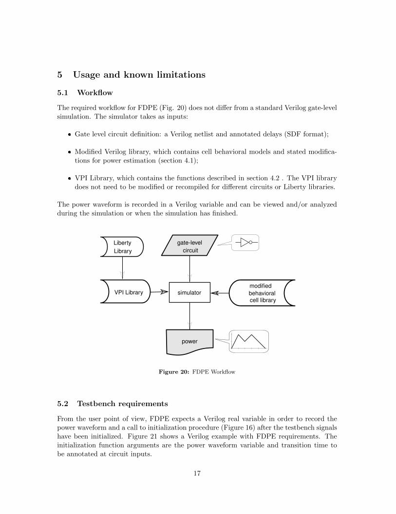
5.1 Workflow
The required workflow for FDPE (Fig. 20) does not differ from a standard Verilog gate-levelsimulation. The simulator takes as inputs:
� Gate level circuit definition: a Verilog netlist and annotated delays (SDF format);
� Modified Verilog library, which contains cell behavioral models and stated modifica-tions for power estimation (section 4.1);
� VPI Library, which contains the functions described in section 4.2 . The VPI librarydoes not need to be modified or recompiled for different circuits or Liberty libraries.
The power waveform is recorded in a Verilog variable and can be viewed and/or analyzedduring the simulation or when the simulation has finished.
gate-levelcircuit
power
modified
cell librarysimulatorVPI Library
LibertyLibrary
behavioral
Figure 20: FDPE Workflow
5.2 Testbench requirements
From the user point of view, FDPE expects a Verilog real variable in order to record thepower waveform and a call to initialization procedure (Figure 16) after the testbench signalshave been initialized. Figure 21 shows a Verilog example with FDPE requirements. Theinitialization function arguments are the power waveform variable and transition time tobe annotated at circuit inputs.
17

1 module testbench ();
3 reg reset , in_data;wire output_data;
5
real pwr_var; // power waveform variable7
parameter tau = 1.27 ; // default transition value in ns9 parameter cap = 0.01 ; // default circuit output capacitance in pF
11 dut_inst dut_module (.in (in_data) ,
13 .reset(reset) ,.out (output_data)
15 );initial begin
17 in_data = 1'b0; // testbench/DUT signl initializationreset = 1'b0; // testbench/DUT signl initialization
19 $fdpe_init("liberty_file.lib","library_name",
21 pwr_var ,tau ,
23 cap ); //FDPE initialization
25 //More code here for DUT stimuli ....
27 endendmodule
Figure 21: Testbench example
5.3 Model time offset adjustment
Depending on timing characteristics of used cells, the waveform offset (section 3.2.1) mayneed to be adjusted, in order to avoid negative delays during simulation.
Notice that the waveform time offset cannot be very large because there is a knownlimitation regarding the waveform time offset (see section 5.4.2).
5.4 Known Limitations
5.4.1 Combinational loops
FDPE does not support combinational loops (e.g. Figure 22). Transition times of pins in acombinational loop path cannot be computed in the initialization procedure (section 4.2.1)because cell input pins transition time must be annotated prior to output transition time,and output transition time depends on the input pins transition time.
An alternative to overcome this limitation is to implement a combinational loop detector,break the loop at a cell input pin, and annotate a default transition time at the brokenconnection. Another alternative is to implement a combinational loop detector and ask theuser where to break the loop, and let the user choose the missing transition time value.
18
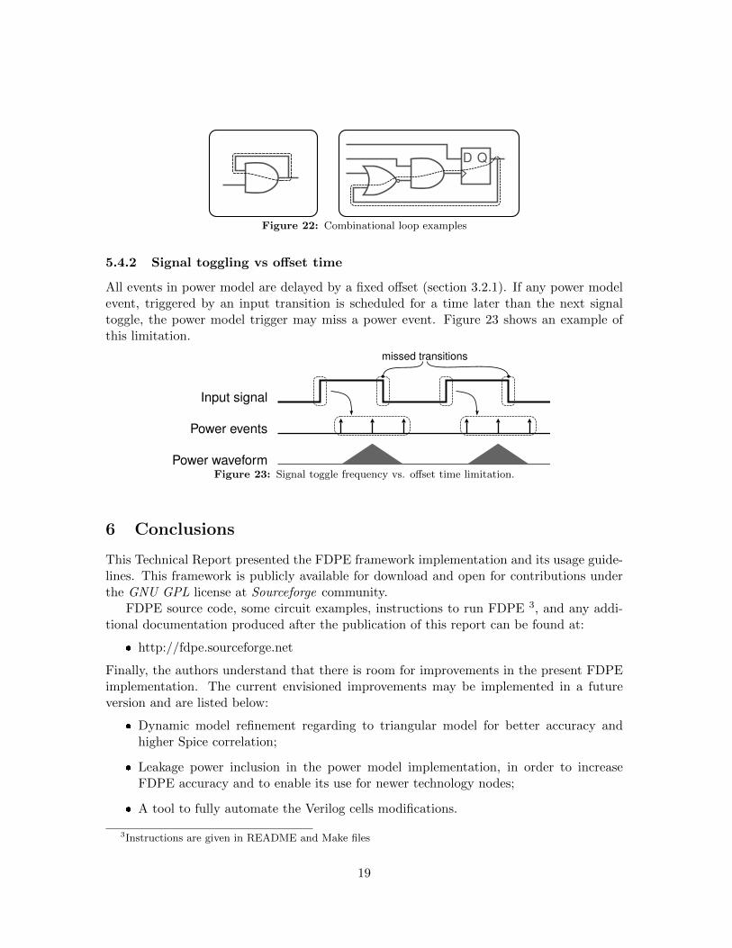
D Q
Figure 22: Combinational loop examples
5.4.2 Signal toggling vs offset time
All events in power model are delayed by a fixed offset (section 3.2.1). If any power modelevent, triggered by an input transition is scheduled for a time later than the next signaltoggle, the power model trigger may miss a power event. Figure 23 shows an example ofthis limitation.
missed transitions
Input signal
Power waveform
Power events
Figure 23: Signal toggle frequency vs. offset time limitation.
6 Conclusions
This Technical Report presented the FDPE framework implementation and its usage guide-lines. This framework is publicly available for download and open for contributions underthe GNU GPL license at Sourceforge community.
FDPE source code, some circuit examples, instructions to run FDPE 3, and any addi-tional documentation produced after the publication of this report can be found at:
� http://fdpe.sourceforge.net
Finally, the authors understand that there is room for improvements in the present FDPEimplementation. The current envisioned improvements may be implemented in a futureversion and are listed below:
� Dynamic model refinement regarding to triangular model for better accuracy andhigher Spice correlation;
� Leakage power inclusion in the power model implementation, in order to increaseFDPE accuracy and to enable its use for newer technology nodes;
� A tool to fully automate the Verilog cells modifications.
3Instructions are given in README and Make files
19

References
[1] M. Rewienski, “A perspective on fast-spice simulation technology,” in Simulation andVerification of Electronic and Biological Systems, pp. 23–42, Springer, 2011.
[2] D. Vidal and M. Cortes, “Fast and Accurate Solution for Power Estimation and DPACountermeasure Design,” in Power and Timing Modeling, Optimization and Simula-tion (PATMOS), 2014 24th International Workshop on, pp. 1–7, Sept 2014.
[3] Liberty, “User guide and reference manual suite.” http://www.opensourceliberty.org. Retrieved: 2015-01-10.
[4] IEEE, “Verilog hardware description language,” IEEE Std 1364-2001, pp. 0–856, 2001.
[5] J. Bhasker and R. Chadha, Static Timing Analysis for Nanometer Designs: A PracticalApproach. Springer, 2009.
[6] D. K. Tala, “Verilog tutorial.” http://www.asic-world.com/verilog/veritut.html.Retrieved: 2015-01-10.
[7] N. Weste and D. Harris, CMOS VLSI Design: A Circuits and Systems Perspective.ADDISON WESLEY Publishing Company Incorporated, 2011.
[8] A. Bogliolo, L. Benini, G. De Micheli, and B. Ricco, “Gate-level power and currentsimulation of cmos integrated circuits,” IEEE Trans. on Very Large Scale Integration(VLSI) Systems, vol. 5, no. 4, pp. 473–488, 1997.
[9] M.-S. Lee, C.-H. Lin, C.-N. J. Liu, and S.-C. Lin, “Quick supply current waveformestimation at gate level using existed cell library information,” in Proc. of the 18thACM Great Lakes Symp. on VLSI, GLSVLSI ’08, (New York, NY, USA), pp. 135–138,ACM, 2008.
[10] M. A. Cirit, “Powerteam�: There is more to verilog beyond behavioral simulation,”2004.
20