institut fÜr technische optik annual report … · the coarse sensor scales are covered by a...
TRANSCRIPT

INSTITUT FÜRTECHNISCHE OPTIKUNIVERSITÄT STUTTGART
annual report2 0 1 1 / 2 0 1 2
INSTITUT FÜR TECHNISCHE OPTIKUNIVERSITÄT STUTTGART
Prof. Dr. W. Osten
ANNUAL REPORT 2011/2012
Pfaffenwaldring 9D-70569 Stuttgart
Tel.: +49(0)711 685-66075Fax: +49(0)711 685-66586
http://www.uni-stuttgart.de/ito

INSTITUT FÜR TECHNISCHE OPTIK, ANNUAL REPORT 2011/2012
another two years filled with many activities in different fields and enriched with fruitful national and world wide cooperation have passed since the ITO staff reported in 2011 about their current research activities. Thus it is again time to inform our partners, sponsors and customers about our recent advances in the field of Applied Optics.
The basic understanding that determines our work remains unchanged: striving for excel-lence in research and teaching, together with a good balance of continuity and systematic renewing. Ongoing activities are directed at both the profound investigation of our strate-gic research topics such as multi-scale sensor fusion, computational microscopy, resolution enhancement, model-based reconstruction, asphere and freeform metrology, hybrid op-tics, digital holography, and optical systems design, and the modernization of our infra-structure. Meanwhile the operation of our reactive ion etching facility has reached the routine level and the Helios Nanolab 600 has been proven as stable and reliable tool for different processing and inspection tasks in the nano world. Our aim to assure flexible structuring technologies with high resolution and reliability not only for a few crucial experi-ments but for making dedicated optical com-ponents is on a good way.
To ensure that ITO can fulfill its mission un-der changing boundary conditions, we have founded in 2008 the cooperative network SCoPE1 at the Stuttgart University. The im-pact of SCoPE is continuously improving and shows encouraging results in the aimed fields: research, teaching and technology transfer. One of the main objectives is the ex-tension of the curriculum in the field of pho-tonic technologies. With the installation of the joint master course in Photonic Engineer-ing, this ambitious goal could be achieved in spring 2013. Scientists from 3 different faculties – physics, electrical engineering and mechanical engineering – are teaching together now the state of the art in Photon-ics. A continuous increase in students can be observed as a welcome trend. Furthermore, several joint research projects are on the way
Dear Reader,

INSTITUT FÜR TECHNISCHE OPTIK, ANNUAL REPORT 2011/2012
and the cooperation with our industrial part-ners is progressing in various fields of com-mon interest.
As a member of the Faculty of Mechanical En-gineering, the Institute represents the Univer-sity of Stuttgart in the field of Applied Optics in research and education. Together with our na-tional and international partners, our research work focuses on the exploration of new op-tical measurement, imaging and design prin-ciples and their implementation in new com-ponents, sensors and sensor systems. One of our long-term central goals is the extension of existing limits by combining modelling, simulation and experimental data acquisition in the context of actively driven measurement processes. Several ambitious objectives are still on our agenda such as the implementa-tion of a multi-sensor measurement systems where the systematic cooperation of different classes of sensors is controlled by a sophisti-cated assistance system, the implementation of our new software system ITOM that helps us to improve the software development for our setups considerably, the completion of the prototype of our new tilted wavefront in-terferometer with the goal of market launch in 2014, and the further improvement of our model-based strategies for the solution of dif-ferent kind of identification problems in optical imaging and metrology.
Our overall research approach “Optical Me-trology and Systems Design” is structured into ten main research directions:
Active Metrology, Model-based Metrology, Remote Metrology, Resolution Enhanced Technologies, Computational Imaging, Sensor Fusion, Sensor Integration, Hybride Optics, Simulation, and Optical Systems Design.
The strong interaction between these direc-tions gives the Institute the required depth across the broad range of our activities in
optics. The considerable number of research projects that are referred to in this report re-flects again the success of this approach.
Besides our wide research activities, an on-going strong commitment of ITO is directed to high-quality teaching on different levels (bachelor, master, PhD). Our consecutive bachelor-master course in medical techno-logy – a joint and challenging project of the University of Stuttgart and the Eberhard Karls Universität Tübingen – is running very successful and enters now the master level. Since the beginning in 2010, ITO is one of the drivers of that course. In 2011 we started a new master course with the dedication “Mechanical Engineering – Micro, Precision and Optical Engineering M.Sc.” and in spring 2013 the mentioned master course “Photonic Engineering M.Sc.” has been implemented.
To cope with our ambitious and extensive approach to Applied Optics, a deep under-standing of physics needs to be combined with practical engineering implementation. This is a daily challenge for all members of the staff. However, a good mixture of gradu-ates in physics and engineering, a vital and innovative scientific climate, that considers the interdisciplinary cooperation with numer-ous national and international institutes, and a continuous observation of the technologi-cal and scientific progress are a good basis to meet these and future challenges.
Stuttgart, July 2013
Wolfgang Osten
1 Stuttgart Research Center of Photonic Engineering, http://www.scope.uni-stuttgart.de/

Index INSTITUT FÜR TECHNISCHE OPTIK, ANNUAL REPORT 2011/2012
Institute structure
Team and structure ........................................................................................................10
Staff of the Institute .......................................................................................................12
Project partners ..............................................................................................................16
Studying optics ...............................................................................................................17
The research groups .......................................................................................................19
Research projects
3D-Surface Metrology
Active inspection of three-dimensional objects using a multi-sensor measurement system .................................................................. 24M. Gronle, W. Lyda, A. Burla, T. Haist, W. Osten
Advanced signal evaluation and line sensors for chromatic confocal spectral interferometry (CCSI/LCSI) ............................................. 27T. Boettcher, M. Gronle, W. Lyda, W. Osten
Design and fabrication of a hybrid hyper-chromatic lens for confocal sensors ............ 29W. Lyda, F. Schaal, C. Pruß, W. Osten
GPU accelerated ray tracing ........................................................................................ 30F. Mauch, M. Gronle, W. Lyda, W. Osten
Model based characterization of confocal measurement systems ............................... 31F. Mauch, W. Lyda, W. Osten
Optical low-cost sensor system for the control of pump rates ..................................... 32K. Körner, W. Lyda, W. Osten
itom – measurement and laboratory automation software .......................................... 33M. Gronle, C. Kohler, M. Wilke, W. Lyda, H. Bieger, W. Osten
Vertically integrated array-type mirau-based OCT system for early diagnostics of skin cancer (VIAMOS) .............................................................. 34W. Lyda, T. Boettcher, J. Krauter, W. Osten
In-situ surface metrology: Integration of a white light interferometer into a high precision grinding machine for diamond tools ............................................. 35W. Lyda, R. Berger, D. Fleischle, W. Osten
Active Optical Systems and Computational Imaging
SLM-based vibrometry ................................................................................................. 38T. Haist, C. Lingel, M. Warber, W. Osten
Index
06

INSTITUT FÜR TECHNISCHE OPTIK, ANNUAL REPORT 2011/2012 Index
07
Optimizing the diffraction efficiency of SLMs:Jones matrix simulation model and time dependent variations .................................... 40C. Lingel, M. Hasler, T. Haist, W. Osten
Fast detection of wavefront disturbance:Holographic modal wavefront sensor ............................................................................41S. Dong, T. Haist, W. Osten
Programmable microscopy ........................................................................................... 42M. Hasler, M. Warber, T. Haist
A systematic method for the description of optical inspection tasks ........................... 44V. Erdogan, W. Osten
High Resolution Metrology and Simulation
Influence of line edge roughness on scatter signatures for CD-metrology .................. 46B. Bilski, K. Frenner, W. Osten
Model-based reconstruction of periodic sub-wavelength structures by white light interference Fourier scatterometry ........................................................ 47V. Ferreras Paz, S. Peterhänsel, K. Frenner, W. Osten
Design of microlenses using plasmonic stacks ............................................................ 49L. Fu, K. Frenner, W. Osten
Improved speckle simulator for rough surfaces using surface integral equations .................................................................................. 50L. Fu, K. Frenner, W. Osten
Reconstruction of dynamical perturbations in optical systems ......................................51H. Gilbergs, K. Frenner
Sub-wavelength imaging with metallic meander structures ....................................... 52P. Schau, L. Fu, K. Frenner, H. Schweizer. H. Giessen, W. Osten
Polarization scrambling with plasmonicmeander-type metamaterials for space applications ..................................................... 54P. Schau, L. Fu, K. Frenner, H. Schweizer. H. Giessen, W. Osten
Depth-sensitive fluorescence measurements for diagnostic investigations ................. 55P. Schau, K. Frenner, W. Osten
Interferometry and Diffractive Optics
The Tilted Wave Interferometer (TWI): A quick and flexible approach to measure asphere and freeform surfaces ................... 58G. Baer, C. Pruß, J. Schindler, W. Osten

Index INSTITUT FÜR TECHNISCHE OPTIK, ANNUAL REPORT 2011/2012
08
Micro optical spatial polarization control ....................................................................... 60F. Schaal, C. Pruß, W. Osten
Fabrication of computer generated holograms on rotationally symmetric curved substrates ..................................................................... 61M. Häfner, C. Pruß, W. Osten
Cost effective production of diffractive multi-level elements ....................................... 63F. Schaal, C. Pruß, W. Osten
Fabrication of diffractive and micro-optical elements for external partners .................. 64F. Schaal, C. Pruß, W. Osten
Phase errors introduced in CGH by rigorous effects ..................................................... 65S. Peterhänsel, C. Pruß, W. Osten
Coherent Metrology
Optical methods for assessment of transport and age induced damages on artworks ............................................................................... 68M. Morawitz, I. Alexeenko, M. Wilke, G.Pedrini, W.Osten
High resolution 3D microscopy using opposed-view dark-field digital holography ......... 69A. Faridian, G. Pedrini, W. Osten
3D UV holographic microscope for biomedical imaging ................................................ 72A. K. Singh, A. Faridian, G. Pedrini, W. Osten
Knowledge management in virtual labs and remote experiments ................................ 73M. Wilke, M. Riedel, G. Situ, I. Alekseenko, G. Pedrini, W. Osten
Compression of digital holograms ................................................................................. 75M. Wilke, G. Pedrini
Nanometric in-plane displacement measurement using phase singularities ............... 76A. K. Singh, G. Pedrini, W. Osten
Short temporal coherence digital holography with a femtosecond frequency comb laser for optical sectioning ........................................ 77K. Körner, G. Pedrini, I. Alexeenko, W. Osten
Holographic recording of incoherently illuminated or self-luminous objects ................ 78D.N. Naik, G. Pedrini, W. Osten
Phase retrieval with resolution enhancement by using random-phase illumination ...... 79P. Gao, G. Pedrini, W. Osten
Structured illumination for resolution enhancement and autofocusing in digital holographic microscopy ..................................................... 80P. Gao, G. Pedrini, W. Osten

INSTITUT FÜR TECHNISCHE OPTIK, ANNUAL REPORT 2011/2012 Index
09
Optical Design and Simulation
Application of complex surfaces in modern optical design ........................................... 82A. Herkommer, C. Pruß, R. Reichle
Phase space methods in geometrical optics ................................................................. 84D. Rausch, A.M. Herkommer
Hybrid endoscopic zoom system with integrated tomographic sensor ........................ 85S. Thiele, A. Herkommer
Publications 2011 - 2012
Invited lectures on international conferences ................................................................ 86
Awards .......................................................................................................................... 87
Editorial work ................................................................................................................. 87
Reviewed papers, books and book chapters ................................................................. 88
Conference proceedings and journals ........................................................................... 92
Patents .......................................................................................................................... 96
Doctoral thesis, diploma thesis & student research thesis ........................................... 98
Colloquia & Conferences
Optik-Kolloquium 2011 ................................................................................................ 100
Optik-Kolloquium 2012 .................................................................................................101
Optik-Kolloquium 2013 ................................................................................................ 102
Organized international conferences: 2011 - 2012 ...................................................... 103

Institute structure INSTITUT FÜR TECHNISCHE OPTIK, ANNUAL REPORT 2011/2012
Team
an
d s
tru
ctu
re
INSTITUTE STRUCTURE

INSTITUT FÜR TECHNISCHE OPTIK, ANNUAL REPORT 2011/2012 Institute structure
11
Ad
min
istr
atio
n, S
oft
war
e En
gin
eeri
ng &
Tec
hn
ical
Su
pp
ort
3D-S
urf
ace
Met
rolo
gy
W. L
yda
Mac
ro a
nd m
icro
m
etro
logy
Whi
te li
ght
and
sp
ectr
al in
terf
erom
etry
Con
foca
l mic
rosc
opy
Frin
ge p
roje
ctio
n
Sen
sor-
mod
els
and
sens
or-f
usio
n
Act
ive
Opt
ical
S
yste
ms
Dr.
T. H
aist
Act
ive
wav
efro
nt
mod
ulat
ion
Act
ive
wav
efro
nt
sens
ors
Ada
ptiv
e op
tics
Com
puta
tiona
l im
agin
g
Dyn
amic
hol
ogra
phy
Hig
h R
eso
luti
on
M
etro
log
y
Dr.
K. F
renn
er
Hig
h re
solu
tion
m
icro
scop
y
Sca
tter
omet
ry
Lig
ht-s
urfa
ce
inte
ract
ion
Mod
elin
g an
d
rigor
ous
sim
ulat
ion
Mod
el-b
ased
re
cons
truc
tion
Inte
rfer
om
etry
an
d D
iffr
acti
ve
Op
tics
F. S
chaa
l
Tec
hnol
ogy
and
co
mpo
nent
s
Des
ign
and
fabr
icat
ion
of d
iffr
activ
e op
tics
Int
erfe
rom
etry
Tes
ting
of a
sphe
res
and
free
form
sur
face
s
Mic
ro-o
ptic
s
Co
her
ent
M
etro
log
y
Dr.
G. P
edrin
i
Op
tica
l Des
ign
an
d S
imu
lati
on
Pro
f. D
r. A
. Her
kom
mer
Dig
ital h
olog
raph
y
Pha
se r
etrie
val
Non
-des
truc
tive
te
stin
g
Exp
erim
enta
l str
ess
an
alys
is
Rem
ote
labo
rato
ries
and
met
rolo
gy
Opt
ical
des
ign
Illu
min
atio
n de
sign
Opt
imiz
atio
n m
etho
ds
Sim
ulat
ion
of
imag
ing
- and
ill
umin
atio
n sy
stem
s
Opt
ical
sys
tem
s in
m
edic
al e
ngin
eerin
g
Ch
air
Pro
f.D
r. W
. Ost
en
Prof
. Dr.
A. H
erko
mm
er
Teac
hin
gE
. Ste
inbe
ißer
Dep
uty
Dr.
T. H
aist
Institute structure INSTITUT FÜR TECHNISCHE OPTIK, ANNUAL REPORT 2011/2012
Director
Prof. Dr. Wolfgang Osten ................ +49 (0) 711 685-66075 [email protected]
Professorship for Optical Design and Simulation
Prof. Dr. Alois Herkommer ............. +49 (0) 711 685-69871 ........ [email protected]
Emeritus
Prof. Dr. Hans Tiziani ....................... +49 (0) 711 685-66077 .................. [email protected]
Administration and Secretary
Katja Costantino .............................. +49 (0) 711 685-69873 .......... [email protected]
Christina Hübl ................................... +49 (0) 711 685-66074................... [email protected]
Christa Wolf ..................................... left on 31.12.2012
Studys
Katharina Bosse-Mettler ................ +49 (0) 711 685-69884 ................. [email protected]
Erich Steinbeißer ............................ +49 (0) 711 685-66068 ....... [email protected]
Scope
Margarita Riedel .............................. +49 (0) 711 685-69893 .................. [email protected]
Research Assistants
3D-Surface metrology
Wolfram Lyda (leader) ....................... +49 (0) 711 685-66594 .................... [email protected]
Dr. David Baureis .............................. +49 (0) 711 685-66650 ............... [email protected]
Tobias Boettcher .............................. +49 (0) 711 685-66656 ........... [email protected]
Dr. David Fleischle ............................ +49 (0) 711 685-69892 [email protected]
Marc Gronle ...................................... +49 (0) 711 685-69888 [email protected]
Dr. Christian Kohler .......................... +49 (0) 711 685-66569 ................. [email protected]
Dr. Klaus Körner ................................ +49 (0) 711 685-66082 [email protected]
Johann Krauter ................................. +49 (0) 711 685-69806 [email protected]
Florian Mauch ................................... +49 (0) 711 685-66835 ................ [email protected]
Staff of the Institute
Status quo: May 2013
12

INSTITUT FÜR TECHNISCHE OPTIK, ANNUAL REPORT 2011/2012 Institute structure
13
Active Optical Systems
Dr. Tobias Haist (leader) .................... +49 (0) 711 685-66069 ................... [email protected]
Shihao Dong ..................................... +49 (0) 711 685-69879 ................. [email protected]
Malte Hasler ...................................... +49 (0) 711 685-69878 ............... [email protected]
Christian Lingel ................................ +49 (0) 711 685-66071 ................ [email protected]
Michael Warber ................................ left on 31.03.2011
Avinash Burla ................................... left on 25.03.2012
High resolution metrology and simulation
Dr. Karsten Frenner (leader) ............. +49 (0) 711 685-66065 ............... [email protected]
Valeriano Ferreras Paz ..................... +49 (0) 711 685-66553 [email protected]
Liwei Fu ............................................. +49 (0) 711 685-69833 [email protected]
Holger Gilbergs ................................ +49 (0) 711 685-66623 .............. [email protected]
Sandy Peterhänsel ........................... +49 (0) 711 685-69875 ...... [email protected]
Philipp Schau .................................... +49 (0) 711 685-69870 ................. [email protected]
Bartosz Bilski .................................... left on 30.09.2012
Interferometry and diffractive optics
Frederik Schaal (leader) ................... +49 (0) 711 685-69883 [email protected]
Goran Baer ........................................ +49 (0) 711 685-66029 [email protected]
Jan Beneke ........................................ +49 (0) 711 685-69877 ............... [email protected]
Alexander Bielke .............................. +49 (0) 711 685-69876 [email protected]
Christof Pruß ................................... +49 (0) 711 685-66066 .................. [email protected]
Johannes Schindler ......................... +49 (0) 711 685-60488 ............ [email protected]
Thomas Schoder ............................. +49 (0) 711 685-66064 [email protected]
Jun Ma ............................................... left on 31.03.2011
René Reichle .................................... left on 30.06.2011
Eugenio Garbusi ............................... left on 31.08.2011
David Hopp ........................................ left on 30.09.2011
Dominik Flöß..................................... left on 29.02.2012
Matthias Häfner ................................ left on 31.01.2013

Institute structure INSTITUT FÜR TECHNISCHE OPTIK, ANNUAL REPORT 2011/2012
Coherent metrology
Dr. Giancarlo Pedrini (leader) .......... +49 (0) 711 685-66078 ................ [email protected]
Dr. Igor Alekseenko .......................... +49 (0) 711 685-66073 [email protected]
Ahmad Faridian ............................... +49 (0) 711 685-69885 ............... [email protected]
Peng Gao .......................................... +49 (0) 711 685-69073 ..................... [email protected]
Henning Kästner .............................. +49 (0) 711 685-69804 ............. [email protected]
Michael Morawitz ........................... +49 (0) 711 685-66528 [email protected]
Dinesh Naik ...................................... +49 (0) 711 685-69078 .................... [email protected]
Alok Kumar Singh ........................... +49 (0) 711 685-69887 .................. [email protected]
Marc Wilke ....................................... +49 (0) 711 685-66076 [email protected]
Mohammadreza Bahrami ................ left on 15.05.2013
Optical Design and Simulation
Prof. Dr. Alois Herkommer (leader) . +49 (0) 711 685-69871 ........ [email protected]
Denise Rausch .................................. +49 (0) 711 685-66648 ................ [email protected]
Simon Thiele ..................................... +49 (0) 711 685-66609 .................. [email protected]
Software Engineering and Technicians
Heiko Bieger ...................................... +49 (0) 711 685-66070 [email protected]
Ralph Knoll ........................................ +49 (0) 711 685-66067 ................... [email protected]
Andreas Lorenz................................. +49 (0) 711 685-66089 ................. [email protected]
Guest Scientists
Dr. Caojin Yuan * .............................. Univ. of Science and ............................................................ Technology Chenggong (China) ................. 12/2009 – 06/2011
Giorgio Pariani .................................. Politecnico di Milano (Italy) .........................10/2010 – 03/2011
Dr. Francisco Salgado-Remacha .... Universidad Complutense ............................................................ de Madrid (Spain) ........................................ 04/2011 – 07/2011
Dr. Vani Chanival .............................. Parul Inst. of Engineering & Techn., ............................................................ Vadodra (India) ............................................ 05/2011 – 07/2011
Prof. Benfeng Bai .............................. Tsinghua University (China) ........................02/2012 – 03/2012
Prof. Anand Krishna Asundi ............ Nanyang University (Singapur) ...................03/2012 – 04/2012
Pavel Pavlicek ................................... Palacky University (Czech Republic) ...........05/2012 – 06/2012
Dr. Dinesh Naik * .............................. The University of Electro- ............................................................ Communication (UEC) (Japan)........................... since 06/2012
Prof. Anhu Li ..................................... Tongji University (China) ............................. 07/2012 – 01/2013
14

INSTITUT FÜR TECHNISCHE OPTIK, ANNUAL REPORT 2011/2012 Institute structure
Larbi Bouamama .............................. Ferhat Abbas University of Setif (Algeria) ..07/2012 – 08/2012
Dr. Peng Gao * .................................. Shenzhen University (China) .............................. since 09/2012
Henri Partanen .................................. Univ. of Eastern Finland (Finland) ................10/2012 – 11/2012
Huarong Gu ....................................... Tsinghua University (China) ............................... since 01/2013
Ruslan Shimansky............................ IA&E SB RAS Novosibirsk (Rusia) ..............01/2013 – 02/2013
Prof. Dr. Mitsuo Takeda ** .............. Utsunomiya University (Japan) ......................... since 03/2013
Foreign Guests visiting the Institute: 2011 – 2012
Prof. Dr. R. Leach .............................. NPL, Teddington, UK .......................................... January 2011
Prof. J. Coupland .............................. Loughborough Univ., UK..................................... January 2011
Prof. Dr. Min Yuung Kim .................. Kyungpook National University, Korea ...............February 2011
Dr. R. Völk .......................................... SUSS Microoptics, Neuchatel ...............................March 2011
Dr. Jiri Novak .................................... Czech Technical University in Prague, Czech Republic ......................................................... May 2011
Prof. Dr. W. Coene ............................ ASML, Veldhoven, Netherlands ...............................May 2011
Prof. Dr. Albertazzi ........................... Univ. Florianopolis, Brazil ..........................................May 2011
Prof. Dr. M. Takeda ........................... UEC, Chofu, Japan ................................................... May 2011
Prof. Dr. B. Javidi .............................. Univ. of Connecticut, Storrs, USA ............................ May 2011
Dr. N. Reingand ................................. Patent Hatchery, Baltimore, USA ............................. May 2011
Dr. C. Gorecki .................................... Univ. Besancon, France ........................................... June 2011
Dr. Arun Anand ................................. Institute for Plasma Research, Gujarat, India .......... June 2011
Prof. Dr. C. Joenathan ...................... Rose-Hulman Inst. of Technology; Terre Haute, USA .......................................................July 2011
Dr. D. Mansfield ................................ Taylor Hobson, Leicecster, UK ...........................October 2011
Prof. Dr. F. Mugele ............................ Univ. Twente, NL ............................................ November 2011
Prof. Dr. P. Bryanston-Cross ............ Univ. Warwick, UK .......................................... November 2011
Prof. Dr. I. Moreno ............................ Univ. Alicante, Spain ....................................... December 2011
Prof. Dr. J. Campos ........................... Univ. Barcelona, Spain .................................... December 2011
Prof. Dr. C. Joenathan ...................... Rose-Hulman Inst. of Technology; Terre Haute, USA .....................................................Febr. 2012
Dr. P. de Groot ................................... Zygo, Middlefield, USA .............................................May 2012
Dr. Arie den Boef .............................. ASML Veldhoven, Netherlands ............................... June 2012
Prof. Dr. C. Joenathan ...................... Rose-Hulman Inst. of Technology; Terre Haute, USA ................................................October 2012
Dr. A. Bernal ...................................... Rose-Hulman Inst. of Technology; Terre Haute, USA ................................................October 2012
15
* Humboldt fellowship ** Humboldt prize-winner and stays at the ITO for altogether one year

Institute structure INSTITUT FÜR TECHNISCHE OPTIK, ANNUAL REPORT 2011/2012
Project collaboration with the following companies and organisations (and many others):
ASML Netherlands B.V. ............................................................................... Veldhoven, Netherlands
Carl Zeiss Microscopy ................................................................................................................ Jena
Carl Zeiss AG .................................................................................................................... Oberkochen
Carl Zeiss SMT AG .......................................................................................................... Oberkochen
Centre Spatial de Liege ..............................................................................................Liege, Belgium
Centre Suisse d’Electronique et de Microtechnique...................................... Zurich, Switzerland
DermoScan GmbH ..................................................................................................................Munich
ESTEC .........................................................................................................Noordwijk, Netherlands
FOS Messtechnik GmbH ...........................................................................................Schacht-Audorf
Fraunhofer ENAS ................................................................................................................. Chemnitz
Fraunhofer IOF ............................................................................................................................. Jena
Fraunhofer IAP .......................................................................................................................Potsdam
Holoeye AG .................................................................................................................................Berlin
HSG-IMAT ...............................................................................................................................Stuttgart
ILM ........................................................................................................................................ Ulm
LaVision GmbH ....................................................................................................................Göttingen
Mahr OKM GmbH ........................................................................................................................ Jena
Polytec GmbH .................................................................................................................... Waldbronn
Robert Bosch GmbH ........................................................................................................... Gerlingen
Shenzhen University .................................................................................................................China
Sick AG ...............................................................................................................................Waldkirch
Siemens AG ..........................................................................................................................München
Staatliche Akademie der Bildenden Künste Stuttgart ....................................................Stuttgart
Statice ..................................................................................................................Besancon, France
Trumpf GmbH + Co. KG .......................................................................................................Ditzingen
Tsinghua University .....................................................................................................Peking, China
Université de Franche-Comté ...............................................................................Besancon, France
University of Eastern Finland ................................................................................Joensuu, Finland
VTT Technical Research Centre of Finland ............................................................. Espoo, Finland
Project partners
16

INSTITUT FÜR TECHNISCHE OPTIK, ANNUAL REPORT 2011/2012 Institute structure
17
Studying optics
Traditionally our curriculum is primarily directed towards the students in upper-level diplom courses of Mechanical Engineering, Cybernetic Engineering, Mechatronics, and Tech-nology Management. Since the academic year 2011/12 this courses are offered as Master courses and an increasing number of master students is going to join our lectures.
This applies especially for the new master programme “Micro-, Precision- and Optical Engineering” which enjoys great popularity also by students from other universities even from other countries.
Since the academic year 2009/10 we also offer our optics courses within the new bachelor and master program “Medical Engineering”, and since 2012 also within the new master program “Photonic Engineering”. We also welcome students from other courses, such as “Physics” and “Electrical Engineering” and “Information Technology”.
The following list should give you an overview about the lectures given at the ITO. Be aware that not all lectures are suitable for all courses and that the lectures are held in Ger-man language.
Core subjects in Master Courses (6 ECTS - Credit Points):
Fundamentals of Engineering Optics Lecture: Prof. Dr. W. Osten
Exercise: H. Gilbergs, E. Steinbeißer
Optical Measurement Techniques and Procedures Lecture: Prof. Dr. W. Osten
Exercise: Dr. K. Körner, E. Steinbeißer
Optical Information Processing Lecture: Prof. Dr. W. Osten
Exercise: Dr. T. Haist, Dr. K. Frenner
Fundamentals of Optics Lecture: Prof. Dr. A. Herkommer
Exercise: D. Rausch
Optical Systems in Medical Engineering Lecture: Prof. Dr. A. Herkommer
Exercise: D. Rausch

Institute structure INSTITUT FÜR TECHNISCHE OPTIK, ANNUAL REPORT 2011/2012
18
Elective subjects in Master Courses (3 ECTS - Credit Points):
Optical Phenomena in Nature and Everyday Life Lecture: Dr. T. Haist
Image Processing Systems for Industrial Applications Lecture: Dr. T. Haist, Dr. Ch. Kohler
Fundamentals of Colorimetry and Digital Photography Lecture: Dr. K. Lenhardt
Polarization Optics and Nanostructured Films Lecture: Dr. K. Frenner
Introduction to Optical Design Lecture: Dr. Ch. Menke, Prof. Dr. A. Herkommer
Current Topics and Devices in Biomedical Optics Seminar: Prof. Dr. A. Herkommer
Additional studies:
project work and thesis within our fields of research (you will find a list of all student project works at the end of this annual report)
practical course “Optic-Laboratory” ==> speckle measurement ==> digital image processing ==> computer aided design of optical systems ==> measurement of the spectral power distribution
practical course “Optical Measurement Techniques” ==> 3D surface measurement applying fringe projection ==> digital holography ==> 2D-interferometry and measurement ==> quality inspection of photo-objectives with the MTF measuring system
common lab for mechanical engineering (APMB)

INSTITUT FÜR TECHNISCHE OPTIK, ANNUAL REPORT 2011/2012 Institute structure
19
3D-Surface Metrology
The objective of the group is the analysis and the implementation of new principles for the acquisition of optical 3D-surface data of engineering and biological objects over a wide scale. Our main focus is on the enhancement of the metering capacity by a combination of physical models and opti-mized system design.
Current research activities are: 3D-measurement applying fringe pro-
jection and deflectometry (macroscopic and microscopic)
adaptive techniques using spatial light modulators
confocal microscopy white light interferometry spectral interferometry sensorfusion and data interpretation
strategies
Contact: [email protected]
Active Optical Systems and Computational Imaging
The objective of our work is the develop-ment of flexible optical systems in order to enable new applications, especially within the field of scientific and industrial metrol-ogy. To achieve this goal, we make use of dif-ferent modern light modulation technologies and computer-based methods. One focus of our work lies in the application of holographic methods based on liquid crystal displays and micromechanical systems for various ap-plications ranging from optical tweezers to aberration control and testing of aspherical surfaces.
Main research areas: active wavefront modulation and
sensors adaptive optics active wavefront sensors dynamic holography components, algorithms, and strategies waveoptical computing computational imaging
Contact: [email protected]
The research groups

Institute structure INSTITUT FÜR TECHNISCHE OPTIK, ANNUAL REPORT 2011/2012
20
High Resolution Metrology and Simulation
The goal of this research group is the in-vestigation of the interaction of light with 3d object structures in the micro and nano do-main. Along with experimental research, one major aspect is the rigorous modelling and simulation as an integral part of the active metrology process.The analysis of all infor-mation channels of the electromagnetic field (intensity, phase, polarisation state of light) allows us to obtain sub-wavelength informa-tion about the structure.
Current research areas: modelling and rigorous simulation computational electromagnetics inverse problems high resolution microscopy scatterometry optical metamaterials
Contact: [email protected]
Interferometry and Diffractive Optics
The goal of our research activity is to ex-plore new measurement concepts using dif-fractive optics. One important application is the testing of optical surfaces, in particular, aspheric lenses. For this purpose we design and produce computer generated holograms (CGH). At the same time, we develop flexible measurement techniques for aspheres and freeform surfaces that aim to replace static null correctors. In addition to CGH for inter-ferometry, our in house production facilities allow us to produce diffractive elements and micro-optics for a wide variety of applications such as imaging systems, UV-measurement systems, beam shaping applications and wavefront sensing.
Our research areas include: testing of aspheric and freeform
surfaces design, fabrication and testing of hybrid
refractive/diffractive systems interferometry and wavefront sensors tailored optics for metrology
applications fabrication of diffractive optics
Contact: [email protected]

INSTITUT FÜR TECHNISCHE OPTIK, ANNUAL REPORT 2011/2012 Institute structure
21
Coherent Metrology
Our research objective is the analysis and application of methods based on coherent optics for the measurement of 3D-shape and deformation and to determine the material properties of technical objects and biological tissues. Aside from the quantitative measure-ments of form and deformation, methods for non destructive material testing are also ana-lysed and applied.
Research areas include: digital holography pulsed holographic interferometry dynamic strain measurements on
biological samples shape measurement wavefront reconstruction holographic non-destructive testing endoscopy remote and virtual laboratories
Contact: [email protected]
Optical Design and Simulation
Focus of the group is the classical optical design of imaging and illumination systems, as well as ray-based and wave-optical sys-tem simulations. Main research targets are the development of novel tools for simulation and optimization and the design of innova-tive complex optical systems for industrial or medical purposes.
Current research topics are: imaging design illumination design optical simulations (ray-tracing and
wave-optical) phase space methods in optical design
and simulation complex surfaces in optical system
design design and simulation of hybrid
optical systems
Contact: [email protected]

RESEARCH PROJECTS
Research projects INSTITUT FÜR TECHNISCHE OPTIK, ANNUAL REPORT 2011/2012

INSTITUT FÜR TECHNISCHE OPTIK, ANNUAL REPORT 2011/2012 Research projects
Active inspection of three-dimensional objects using a multi-sensor measurement system .................................................................. 24 Supported by: Baden-Württemberg Stiftung Project: “AMuPrüf”
Advanced signal evaluation and line sensors for chromatic confocal spectral interferometry (CCSI/LCSI) .............................................. 27 Supported by: DFG (OS 111/21-1/2/3) Project: “Chromatisch-konfokale Spektral-Interferometrie zur dynamischen Profilerfassung”
Design and fabrication of a hybrid hyper-chromatic lens for confocal sensors ............ 29 Project: “R&D-Study for ProMicron, Germany”
GPU accelerated ray tracing ........................................................................................ 30 Supported by: BMBi (FKZ 13N7861) Project: “PräziLED”
Model based characterization of confocal measurement systems ............................... 31 Supported by: BMBF (FKZ 13N10386) Project: “OptAssyst”
Optical low-cost sensor system for the control of pump rates ..................................... 32 Supported by: AIF, IGF-No.: ZN09560/09, ITO project No.: 16653 NProject: “Optical measurement system for estimation of the position of the piston in a one-way dosing pump“
itom – measurement and laboratory automation software ........................................... 33
Vertically integrated array-type mirau-based OCT system for early diagnostics of skin cancer (VIAMOS) .............................................................. 34Supported by: EU (Call FP7-ICT-2011-8). Project: “Vertically Integrated Array-type Mirau-based OCT System for early diagnostics of skin cancer”
In-situ surface metrology: Integration of a white light interferometer into a high precision grinding machine for diamond tools ............................................. 35Supported by: BMWi (FKZ 16IN0519)Project: “iTool”
3D-Surface Metrology
23

24
In the manufacturing process of compo-nents with complex three-dimensional surfac-es, there is a growing demand for consistent quality control, calling for fast, reliable and flex-ible inspection systems. Considering complex objects, it is a common insight, that this de-mand cannot be met in a single measurement step. Instead, different inspection steps have to be applied to different sub-regions on the object. Within these sub-regions, defects with varying characteristics, regarding e.g. their size or their general form, have to be detected and analyzed. In order to realize such a manifold in-spection task, a flexible multi-sensor measure-ment system is implemented. It may consist of a set of different sensors, each having individ-ual properties that are located at different posi-tions in the area of conflict consisting of the resolution, measurement speed and field size.
The focus of the project “AMuPrüf” lies in the development of a flexible inspection sys-tem for finding different defects on the surface of small gears. At first, a meshed model of the gear is created based on the common set of parameters, like its module or number of teeth. The surface of the gear can now be split into some main functional sub-regions, where each region must confirm a certain set of specifica-tions. The objective of the overall inspection system is to verify these given specifications. An example might be that no defects of the general type “scratch” must be on the surface whose dimensions exceed a given limit.
In order to realize a successful and flexible system for inspecting varying specifications, the following challenges have to be considered and overcome:
Active inspection of three-dimensional objects using a multi-sensor measurement system
M. Gronle, W. Lyda, A. Burla, T. Haist, W. Osten
Usually, large areas have to be searched for very small defects. Additionally, the size and shape of each defect may also vary with respect to the type of gear or specification. Due to the limited space-bandwidth-product of optical sensors, it would need a lot of time in order to sample the whole surface with a high-precision sensor. To balance this conflict, a multi-scale measurement strategy with mul-tiple sensors fused in one system is utilized to characterise the surface at different scales. This strategy follows an iterative exploration strategy, where a combination of a coarse scale sampling together with an adapted data analysis (indicator function) provides hints where defects may lie, such that the system only needs to resample these regions of inter-est with sensors working in finer scales until the final result can be achieved.
A hardware assistant system helps the user to select an appropriate set of sensors includ-ing their ideal parameterization for realizing this multi-scale inspection system with respect to the given general task.
Due to the complex surface structure of ob-jects like gears, a high precision positioning system together with an appropriate software package is needed in order to optimally posi-tion the object with respect to each sensor. Additionally, an enhanced extrinsic calibration strategy has been developed, such that the relative position of each sensor in one global coordinate system is known. Then, the data sets, acquired at different positions and in dif-ferent scales, can be merged together in one common system and compared with the given model of the inspected object.
Research projects INSTITUT FÜR TECHNISCHE OPTIK, ANNUAL REPORT 2011/2012

25
The demonstrator for the inspection of gears is based on a modified Mahr MFU 100 (Fig. 1.) which contains of three translational axes and one axis of rotation. The mounted sensors are one scalable fringe projection microscope (based on a Leica microscope MZ 12.5) whose magnification can be switched between 0.8x and 10.0x. Additionally the sensor in the fin-est scale is a chromatic confocal point sensor CHRocodile E (Precitec).
Figure 2 shows an example for detecting a scratch on one face of a gear using the multi-scale inspection strategy. The fringe projection microscope samples the surface with a low magnification in order to obtain a quick over-view measurement that is afterwards correlat-ed with a polygonal model of the gear. Based on the model, the faces are indicated and mea-sured again with a more precise sensor. Then, another indicator function marks a sub-regions, where the given specification (here: a scratch
Fig. 1: Automated multi-scale inspection system based on a modified Mahr MFU 100. The coarse sensor scales are covered by a scalable fringe projection microscope while a chromatic confocal point sensor is used for high-precision measurements in the finest scale.
Fig. 2: Multi-scale inspection cycle for the examination of a scratch on one face of the gear.
INSTITUT FÜR TECHNISCHE OPTIK, ANNUAL REPORT 2011/2012 Research projects

26
on the surface) is possibly not met. By repeat-ing this procedure using the scalable sensor, the final decision is taken in the third scale, where the defect can be clearly resolved and characterized.
For an automatic and optimal definition of appropriate indicator functions, a software as-sistant system has been developed. The input to this system is a library of real measurement data together with marked defects in each im-age. Using an optimization algorithm based on genetic programming, a chain of basic image processing steps together with the appropri-ate set of parameters is selected, such that the marked regions are automatically determined out of the training data set. An example for the indication of a scratch in the intensity image of one single acquisition is depicted in figure 3.
Finally, the actuators, sensors and assistant systems are combined in one complex soft-ware, which still is under development and further has to be equipped with a field of view planning in order to optimally position the sen-sor with respect to the object’s surface, con-sidering the shape and local gradient of the object as well as the general visibility of the region by a certain sensor at a specific position.
Supported by: Baden-Württemberg StiftungProject: “AMuPrüf"
References:
[1] Burla, A.; Haist, T.; Lyda, W.; Aissa, M. H.; Osten, W. „Assis-tant systems for efficient multiscale measurement and inspec-tion“, Proc. SPIE 8082 (2011).
[2] Lyda, W.; Burla, A.; Haist, T.; Gronle, M.; Osten, W. „Imple-mentation and Analysis of an Automated Multiscale Measure-ment Strategy for Wafer Scale Inspection of Micro Electrome-chanical Systems”, IJPEM 13 (2012).
[3] Gronle, M.; Lyda, W.; Burla, A.; Osten, W. “Extrinsic calibra-tion of a fringe projection sensor based on a zoom stereo mi-croscope in an automatic multiscale measurement system”, Proc. SPIE 8430 (2012).
[4] Burla, A.; Haist, T.; Lyda, W.; Osten, W. „Software Assistant System for Automatic Algorithm Design and Configuration in Multiscale Inspection based on Genetic Programming“, Opt. Eng. 51(6) (2012).
[5] Gronle, M.; Lyda, W.; Osten, W. “Concepts for an active in-spection of three-dimensional objects using a multi-sensor measurement system”, Proc. Optics and Measurement, Li-berec, CZ (2012).
Research projects INSTITUT FÜR TECHNISCHE OPTIK, ANNUAL REPORT 2011/2012
Fig. 3: Image processing algorithm in order to indicate the position of the scratch in the input image. The algorithm has been created and optimized using genetic program-ming based on a set of training data.

27
Chromatic confocal spectral interfero- metry (CCSI) is a hybrid measurement method for fast topography measurement without mechanical axial scan. The CCSI-method combines the advantages of the interfero-metric gain and accuracy with the robustness of confocal microscopy. A one shot measure-ment is achieved by using chromatically se-parated foci in the object space and a spectral detection of the white light signal.
In common used spectral interferometers (SI) the measurement range is given by the depth of focus leading to a restriction of the numerical aperture. The combination of chromatic separation and confocal filtering decouples the measurement range from the depth of focus, which yields higher numeri-cal apertures and improved lateral resolution in comparison to common SI-sensors. The advantage of this method is the single shot retrieval of depth positions by either confo-cal signal analysis or optical path evaluation. Hence CCSI is qualified for high resolution topography measurements of reflecting and scattering objects.
The discrepancy of the limited axial range in previously reported SI-schemes can be vi-sualised as follows. The reference field con-tains a planar wave front, while the detection wave front acquires a rigorous curvature, when the object lies beyond the depth-of-fo-cus, if aberration effects are neglected. Op-
Advanced signal evaluation and line sensors for chromatic confocal spectral interferometry (CCSI/LCSI)
T. Boettcher, M. Gronle, W. Lyda, W. Osten
tical interference between those two fields leads to a reduced contrast of the modulated spectral signal. In the CCSI-scheme pre-sented here, the axial range of the detector is expanded due to the chromatically-dispersed foci by means of a diffractive optical element (DOE). If the object lies within the dispersed focus spectrum, a sharply focused spectral component gets reflected and this induces a high-contrast wavelet in the spectral domain. The amplitude of this modulation remains constant within the entire range of the opti-cal spectrum employed and the axial range of the detector is decoupled from the limited depth-of-focus.
Fig. 1 shows the current Linnik-type set-up, where CCSI can easily be compared to standard Chromatic Confocal Microscopy (CCM), using the same optical components and a shutter to switch the reference arm on (CCSI) or off (CCM). An axial measurement range of 18µm up to 100µm is achieved with 50x/0.8 NA or 20x/0.46 NA microscope ob-jectives respectively, where a spectral range from 810 nm to 870 nm is provided by a Su-perluminescent Diode (SLD).
As shown in Fig. 2, the evaluation of the wavelets envelope from a CCSI measure-ment shows the same result as a CCM mea-surement. Utilizing the interferometric infor-mation with a lockin phase evaluation leads to a significantly better result.
Fig. 1: Linnik-type demstrator setup for direct comparison of CCM and CCSI.
Fig. 2: Measurement of resolution standard Simetrics RS-N at 4µm pitch with CCM and CCSI, evaluating both, enve-lope and lockin phase.
INSTITUT FÜR TECHNISCHE OPTIK, ANNUAL REPORT 2011/2012 Research projects

28
Furthermore, the Laterally Chromatically dispersed, Spectrally encoded Interferom-eter (LCSI), a new concept of a one-shot line sensor based on spectral interferometry has been presented. In this design, the spectral separation by a blazed grating leads to a il-luminated line of about 1mm length, where every point is spectrally encoded. Thus, the interference signal depends on both, the lat-eral position and the optical path difference (OPD) induced by the height profile of the specimen. The OPD is usually retrieved from the derivative of the phase term of the signal. In LCSI, for all n pixels of the spectrometer, this derivation leads to a differential equation, which for a single shot measurement can be solved, if a raw estimation on the monoto-nicity of the phase evolution can be derived from a priori information. Based on first order taylor approximation, one gets n-1 additional equations, leading to a underdetermined system of linear equations. At least one ad-ditional equation is needed to retrieve a solu-
tion. In many cases, this additional equation can be derived from a simple model of the measured surface, e.g. symmetry consider-ations. By this approach, precise results can be achieved as shown in Fig. 4.
If the specimen is slightly shifted, every point is illuminated by a second wavenum-ber, leading to another set of equations. Due to the slight shift, the wavenumber is also only changed by a low value, thus the Signal-to-Noise Ratio drops significantly.
To overcome this limitation, in the current project (DFG OS111/21-3), the LCSI setup will be expanded by a second light source as shown in Fig. 3. The spectral distribution will feature a peak wavelength of 415nm and a bandwidth of about 20 nm. Thus, both light sources can use the same blazed grating for spectral separation. As both light sources provide an independent set of equations, lo-cal measurement errors do not globally com-promise the result and the measurement principle gets more robust.
Supported by: DFG (OS 111/21-1/2/3) Project: “Chromatisch-konfokale Spektral-Inter-ferometrie zur dynamischen Profilerfassung”
References:
[1] European patent EP 1 805 477 B1, Interferometrisches Ver-fahren und Anordnung (2005).
[2] German patent DE 10 2008 020 902 B4, „Anordnung und Verfahren zur konfokalen, spektralen Zweistrahl-Interferom-etrie“ (2008).
[3] Gronle, M. et al. “Laterally chromatically dispersed, spectrally encoded interferometer”, Applied Optics 50, 23, 4574-4580 (2011).
[4] Lyda, W. et al. “Advantages of chromatic-confocal spectral interferometry in comparison to chromatic confocal micros-copy”, Measurement Science and Technology 23, 5, 54009 (2012).
[5] Mauch, F. et al., Improved signal model for confocal sensors accounting for object depending artifacts, Optics Express 20, 18, 19936-19945 (2012).
Fig. 3: LCSI scheme with second light source.
Research projects INSTITUT FÜR TECHNISCHE OPTIK, ANNUAL REPORT 2011/2012
Fig. 4: Measurement of chirped calibration specimen by PTB with the LCSI sensor. Model based approach without lateral shift is used, axial symmetry assumed.

29
Chromatic confocal microscopy is a single shot measurement principle which offers fast, accurate and robust measurement data. In the past years several commercial point and line sensors with submicron accuracy and nanometer resolution for shop floor en-vironment were developed. To take advan-tage of this high resolution the actuators of the inspection systems have to meet tight requirements on straightness and flatness. The high price of such systems limits their deployment to medium and large production facilities.
The objective of the overall project was to develop an add-on sensor module based on chromatic confocal microscopy for common-ly used shop floor microscopes to reduce the necessary capital investment for such type of sensors.
On sub-contractual basis ITO designed and fabricated the hyper-chromatic element for the chromatic dispersion. The element consists of a positive refractive lens and a diffractive optical element (negative Fresnel-lens). By balancing the refraction power of both elements for the center wavelength the measurement range of the sensor is centered around the focal plane of the classical bright field illumination of the system. To switch be-tween classical bright field illumination and point-wise distance measurement mode the element was mounted into the DIC prism re-volver of the microscope (see Fig. 1).
The optical element was fabricated at ITO. It is a hybrid diffractive/refractive lens, where the diffractive structures were fabricated on the planar side of a plano-convex lens. Core of our CGH fabrication is the laser writing system CLWS300, a flexible high precision tool that works in polar coordinates, compa-rable to a DVD writer. This working principle offers the advantage of a high, continuous scanning speed and facilitated fabrication of rotationally symmetric structures. Yet the system is not limited to writing circles but al-lows to write arbitrary structures such as lin-ear gratings, microlenses or angular scales. It is capable of writing both binary and blazed diffractive optical elements. Blazed struc-tures are written in grayscale mode where the writing beam intensity is varied with at
Design and fabrication of a hybrid hyper-chromatic lens for confocal sensors
W. Lyda, F. Schaal, C. Pruß, W. Osten
the moment up to 256 levels.The substrate size can vary from a few mil-
limeters to 300 mm in diameter. The shape can be rectangular, round or any other rea-sonable outline. The system allows substrate thicknesses up to 25 mm.
The resulting photoresist profile is then either used directly (e.g. for mastering) or is transferred into the fused silica substrate us-ing dry etching (RIE).
INSTITUT FÜR TECHNISCHE OPTIK, ANNUAL REPORT 2011/2012 Research projects
Project: “R&D-Study for ProMicron, Germany”
References:
[1] Körner, K.; Ruprecht, A. “German Patent Appl. DE 103 21 885 A1 (2003)
Fig. 1: Design of the hybrid optical element based on a diffrac-tive optical element with negative focal length and a refractive lens with positive focal length. The combined focal length for the design wavelength is zero
Fig. 2: Chromatic dispersion of the hybrid element.
30
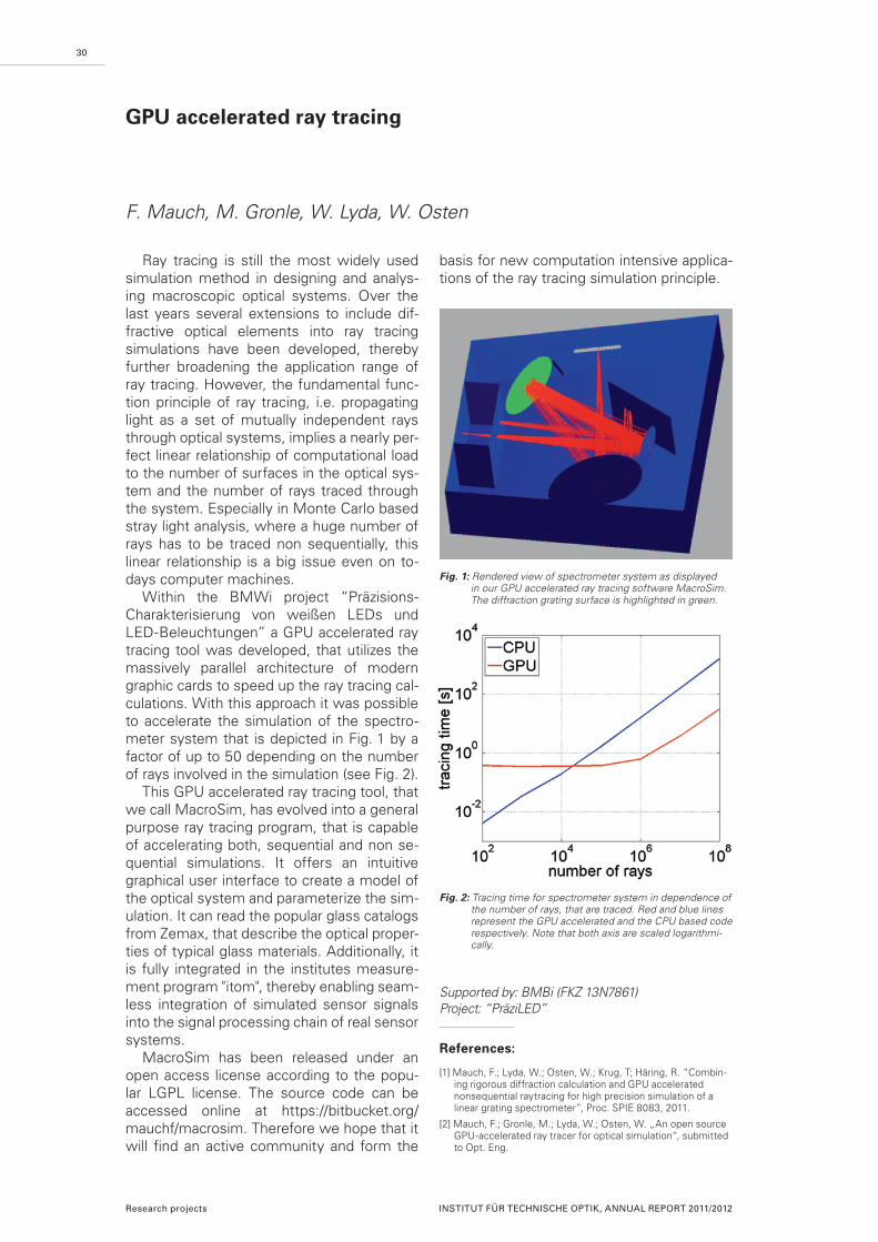
Ray tracing is still the most widely used simulation method in designing and analys-ing macroscopic optical systems. Over the last years several extensions to include dif-fractive optical elements into ray tracing simulations have been developed, thereby further broadening the application range of ray tracing. However, the fundamental func-tion principle of ray tracing, i.e. propagating light as a set of mutually independent rays through optical systems, implies a nearly per-fect linear relationship of computational load to the number of surfaces in the optical sys-tem and the number of rays traced through the system. Especially in Monte Carlo based stray light analysis, where a huge number of rays has to be traced non sequentially, this linear relationship is a big issue even on to-days computer machines.
Within the BMWi project “Präzisions-Charakterisierung von weißen LEDs und LED-Beleuchtungen” a GPU accelerated ray tracing tool was developed, that utilizes the massively parallel architecture of modern graphic cards to speed up the ray tracing cal-culations. With this approach it was possible to accelerate the simulation of the spectro-meter system that is depicted in Fig. 1 by a factor of up to 50 depending on the number of rays involved in the simulation (see Fig. 2).
This GPU accelerated ray tracing tool, that we call MacroSim, has evolved into a general purpose ray tracing program, that is capable of accelerating both, sequential and non se-quential simulations. It offers an intuitive graphical user interface to create a model of the optical system and parameterize the sim-ulation. It can read the popular glass catalogs from Zemax, that describe the optical proper-ties of typical glass materials. Additionally, it is fully integrated in the institutes measure-ment program "itom", thereby enabling seam-less integration of simulated sensor signals into the signal processing chain of real sensor systems.
MacroSim has been released under an open access license according to the popu-lar LGPL license. The source code can be accessed online at https://bitbucket.org/mauchf/macrosim. Therefore we hope that it will find an active community and form the
GPU accelerated ray tracing
F. Mauch, M. Gronle, W. Lyda, W. Osten
basis for new computation intensive applica-tions of the ray tracing simulation principle.
Supported by: BMBi (FKZ 13N7861)Project: “PräziLED”
References:
[1] Mauch, F.; Lyda, W.; Osten, W.; Krug, T; Häring, R. “Combin-ing rigorous diffraction calculation and GPU accelerated nonsequential raytracing for high precision simulation of a linear grating spectrometer”, Proc. SPIE 8083, 2011.
[2] Mauch, F.; Gronle, M.; Lyda, W.; Osten, W. „An open source GPU-accelerated ray tracer for optical simulation“, submitted to Opt. Eng.
Fig. 1: Rendered view of spectrometer system as displayed in our GPU accelerated ray tracing software MacroSim. The diffraction grating surface is highlighted in green.
Fig. 2: Tracing time for spectrometer system in dependence of the number of rays, that are traced. Red and blue lines represent the GPU accelerated and the CPU based code respectively. Note that both axis are scaled logarithmi-cally.
Research projects INSTITUT FÜR TECHNISCHE OPTIK, ANNUAL REPORT 2011/2012
31
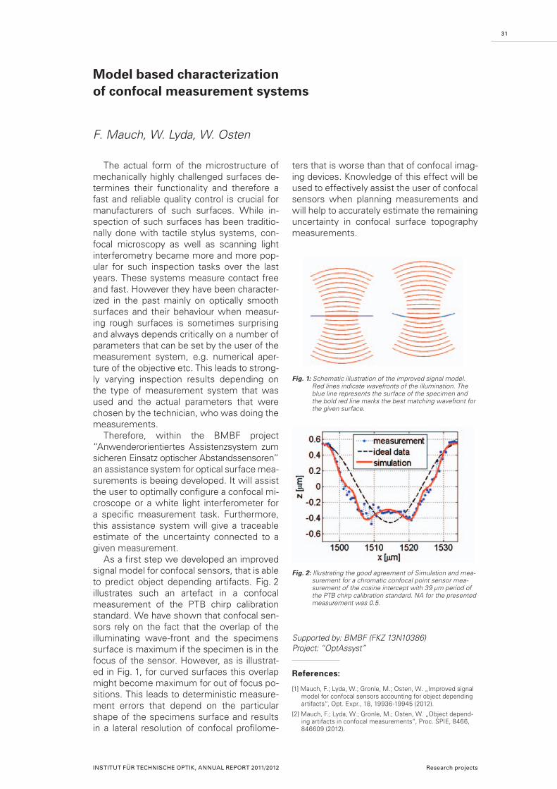
The actual form of the microstructure of mechanically highly challenged surfaces de-termines their functionality and therefore a fast and reliable quality control is crucial for manufacturers of such surfaces. While in-spection of such surfaces has been traditio-nally done with tactile stylus systems, con-focal microscopy as well as scanning light interferometry became more and more pop-ular for such inspection tasks over the last years. These systems measure contact free and fast. However they have been character-ized in the past mainly on optically smooth surfaces and their behaviour when measur-ing rough surfaces is sometimes surprising and always depends critically on a number of parameters that can be set by the user of the measurement system, e.g. numerical aper-ture of the objective etc. This leads to strong-ly varying inspection results depending on the type of measurement system that was used and the actual parameters that were chosen by the technician, who was doing the measurements.
Therefore, within the BMBF project “Anwenderorientiertes Assistenzsystem zum sicheren Einsatz optischer Abstandssensoren” an assistance system for optical surface mea-surements is beeing developed. It will assist the user to optimally configure a confocal mi-croscope or a white light interferometer for a specific measurement task. Furthermore, this assistance system will give a traceable estimate of the uncertainty connected to a given measurement.
As a first step we developed an improved signal model for confocal sensors, that is able to predict object depending artifacts. Fig. 2 illustrates such an artefact in a confocal measurement of the PTB chirp calibration standard. We have shown that confocal sen-sors rely on the fact that the overlap of the illuminating wave-front and the specimens surface is maximum if the specimen is in the focus of the sensor. However, as is illustrat-ed in Fig. 1, for curved surfaces this overlap might become maximum for out of focus po-sitions. This leads to deterministic measure-ment errors that depend on the particular shape of the specimens surface and results in a lateral resolution of confocal profilome-
Model based characterization of confocal measurement systems
F. Mauch, W. Lyda, W. Osten
ters that is worse than that of confocal imag-ing devices. Knowledge of this effect will be used to effectively assist the user of confocal sensors when planning measurements and will help to accurately estimate the remaining uncertainty in confocal surface topography measurements.
Supported by: BMBF (FKZ 13N10386)Project: “OptAssyst”
References:
[1] Mauch, F.; Lyda, W.; Gronle, M.; Osten, W. „Improved signal model for confocal sensors accounting for object depending artifacts“, Opt. Expr., 18, 19936-19945 (2012).
[2] Mauch, F.; Lyda, W.; Gronle, M.; Osten, W. „Object depend-ing artifacts in confocal measurements“, Proc. SPIE, 8466, 846609 (2012).
Fig. 1: Schematic illustration of the improved signal model. Red lines indicate wavefronts of the illumination. The blue line represents the surface of the specimen and the bold red line marks the best matching wavefront for the given surface.
Fig. 2: Illustrating the good agreement of Simulation and mea-surement for a chromatic confocal point sensor mea-surement of the cosine intercept with 39 µm period of the PTB chirp calibration standard. NA for the presented measurement was 0.5.
INSTITUT FÜR TECHNISCHE OPTIK, ANNUAL REPORT 2011/2012 Research projects

32
For the enhancement of a one-way dosing pump, we investigated approaches for the highly resolved optical measurement of the position of the piston, see Fig. 1. The main objective is to ensure a high resolution and a low measurement uncertainty in the rate of fluid delivery from 10 µl/min to 100 ml/min with the same pump module. The industrial application requires both, a very robust and a low-cost solution.
So we applied a low-cost microscopic approach with a small magnification that directly detects the illuminated lip of the mo-ving seal of the pump. For achieving the aims mentioned above, the resolution of the posi-tion of the sealing lip has to be in the submi-cron range. That means sub-pixel accuracy. For this, we use a correlation based method in a sequence of images of the sealing lip for precise detecting the motion of this lip in combination with a Lab-view control loop.
First, we applied a commercially available telecentric lens for detecting the lip position. Fig. 2 shows the calculated movement of the sealing lip in the liquid medium Lipofundin at a pump rate of 5 ml/h, and Fig. 3 presents the calculated mass of the shifted medium over time. Considering linearity, both curves are the same. However, there is a significant difference of about 6% between the opti-cal measurement and the measured mass of a scale. Further investigations showed the not negligible influence of the evapora-tion of the water content in Lipofundin in our experiments. Another error in measurement is probably caused by synchronization prob-lems of Labview during load stroke of the metering pump.
Secondly, we designed, manufactured and tested a telecentric optical stage with two diamond turned lenses made of acryl glass (PMMA) for proving a low-cost approach for mass production. First results show the tech-nical applicability of that approach.
A very first market analysis of the ne-cessary sensor components including LED illumination and microcontroller provided evidence: The costs for the whole sensor system will not exceed 100 € in case of mass production (1000 sensors a year).
There are widespread application fields for
Optical low-cost sensor system for the control of pump rates
K. Körner, W. Lyda, W. Osten
this technical concept also where aggressive fluids have to be used, for example in medi-cal care, chemical industry, biotechnology or pharmacy.
Supported by: AIF, IGF-No.: ZN09560/09, ITO project No.: 16653 NProject: “Optical measurement system for estima-tion of the position of the piston in a one-way dosing pump“Project partner: HSG-IMAT
References:
[1] Wolter, F.; Fritz, K.-P.; Kück, H.; Körner, K.; Lyda, W.; Burla, A. “Sensor-controlled metering pump with disposable pump unit”, Proc. of the ACTUATOR, Bremen, 2012.
Fig. 1: One-way pump element (syringe) with an optical low cost sensor (courtesy of HSG-IMAT).
Fig. 2: Optically detected and by a Labview program calculated shift of the sealing lip in the liquid medium Lipofundin, pump rate 5ml/h. (pump system: HSG-IMAT).
Fig. 3: Calculated mass over time of medium Lipofundin, pump rate 5ml/h (pump system: HSG-IMAT).
Research projects INSTITUT FÜR TECHNISCHE OPTIK, ANNUAL REPORT 2011/2012

33
Both the development of new optical sensors and the operation of such systems for instance in a laboratory environment require a fast and flexible software system. This software has to be able to communicate with a wide range of different hardware systems, such as cameras or actuators and should provide a diversified and as complete as possible set of evaluation and data processing methods. Additionally, the rapid prototyping of modern measurement and inspection setups requires a system, where pa-rameters or components can easily be changed at runtime, necessitating the availability of an embedded scripting language. Finally, when operating a measurement system, it is also de-sirable to extend the graphical user interface by system adapted dialogs and windows.
Since no commercial software system fits all these requirements within the desired perform-ance and quality parameters, a group at ITO started to design and program the new mea-surement software “itom” in 2011, partially in-spired by the former ITO-software “m”.
It mainly consists of four pillars:1. The core application with its graphical user
interface (GUI) gives access to the most impor-tant functions of “itom” without further need for scripting or programming any code.
2. The plugin system. The main idea behind “itom” was to keep the core application thin. Therefore, “itom” can be extended by external libraries (plugins), that are dynamically loaded at runtime . One group of plugins provides access to any hardware systems “itom” should be able to communicate with. Other plugins contain data processing and analysis algorithms as well as complex user interfaces like win-dows or dialogs. The last group of plugins provides plotting and figure components in order to show live images of cameras or visualize other data structures.
3. The popular and
"itom" – measurement and laboratory automation software
M. Gronle, C. Kohler, M. Wilke, W. Lyda, H. Bieger, W. Osten
powerful scripting language Python is embed-ded in “itom”. It is possible to use Python and the functionalities provided by such freely avail-able modules as Numpy, Scipy or Matplotlib, within “itom”. Additionally, a Python-module itom acts as an interface to the core applica-tion “itom” as well as its plugins. The scripting system provides full development functionality, including language support and debugging.
4. Measurement systems can be extended by their own GUIs. A WYSIWYG design tool is available, allowing connection of interface ele-ments to scripted functionalities. As a result, us-ers can configure the appearance of their mea-surement system to optimally enable or protect the underlying functionalities.
The application “itom” itself is programmed in C++ using the open source framework Qt. This framework enhances the functionality of C++, mainly by providing a cross-platform GUI, allowing “itom” to run on both Windows and Linux operating system. The design of “itom” focuses on the support of modern, multi-core processors by making extensive use of multi-threading, effectively running script execution, hardware control and algorithmic plugins each in their own separate threads. As a result, com-putationally demanding algorithms can be exe-cuted or an actuator can slowly move while the main application is still kept reactive.
The core application of “itom” is released un-der the open source license LGPL. The sources can be freely downloaded from the internet at https://bitbucket.org/itom.
Fig. 1: Screenshot of itom software on a Windows operating system.
INSTITUT FÜR TECHNISCHE OPTIK, ANNUAL REPORT 2011/2012 Research projects

34
Skin cancer is one of the most commonly diagnosed type of cancer with an increasing number of cases in the last years. Most cas-es are caused by over-exposure to UV-light. If the cancer is untreated, it becomes fatal. If the cancer is diagnosed in an early state, it can be treated effectively. Hence an efficient and easy-to-use diagnostic tool is necessary.
The current state of the art is a visual in-spection either by clinicians or self-exami-nations. If cancer is assumed, the potential melanoma is removed and a traditional bi-opsy is applied as a reference diagnosis. The drawbacks of this technique are the long di-agnosis time of several days to weeks and the invasiveness of the procedure, but the advantages are a good image quality and high contrast between malign and belign tis-sue. Hence non-invasive imaging methods have been developed.
Two methods which match the require-ments on the resolution are confocal mi-croscopy and optical coherence tomography (OCT). Both offer a resolution down to some microns and sufficient penetration depth. They offer a non-invasive 3D-visualisation of the human skin. While confocal microscopy offers a higher resolution, OCT has a higher penetration depth along with a short data ac-quisition time.
The disadvantage of the current systems is the high system cost up to 100 k€, limiting the application to bigger hospitals.
The project VIAMOS aims to reduce the cost of such OCT systems dramatically. Therefore a small handheld, low-cost, OCT device will be developed which is 10 times cheaper and 150 times smaller than cur-rent systems. This will be achieved by mod-ern 3D-packaging techniques and direct integration of waver level optics and micro mechanical optical systems like the sys-tem architecture based on a parallel Mirau layout developed in the EU-project “Smar-thies”. The targeted measurement volume is 5 mm x 5 mm x 0.5 mm with an acquisition time under 20 seconds. The challenge will be to cope with the low contrast between differ-ent kind of tissue compared to biopsy.
Vertically integrated array-type mirau-based OCT system for early diagnostics of skin cancer (VIAMOS)
W. Lyda, T. Boettcher, J. Krauter, W. Osten
The project consortium brings together aca-demic institutions, research institutes and in-dustrials partners, experienced in the field of MEMS & MOEMS, photonics & OCT, micros-copy, system integration and dermatology.
More information under www.viamos.eu.
Supported by: EU (Call FP7-ICT-2011-8). Project: “Vertically Integrated Array-type Mirau-based OCT System for early diagnostics of skin cancer”Project coordinator: Prof. Christophe Gorecki, FEMTO-ST/ Université de Franche-Comté, France
Project consortium: Institute FEMTO-ST, UFR Sciences Médicales et Pharmaceutiques, Université de Franche-Comté, France
VTT Technical Research Centre of Finland. Institut für Technische Optik, University of Stuttgart, Germany
Fraunhofer-Einrichtung für Elektronische Nanosys-teme, ENAS, Chemnitz, Germany
Swiss Center for Electronics and Microtechnology, CSEM SA, Switzerland
DermoScan GmbH, Regensburg, Germany Statice, Besançon, France
Fig. 1: VIAMOS-Logo
Research projects INSTITUT FÜR TECHNISCHE OPTIK, ANNUAL REPORT 2011/2012

35
Diamond tools are used to fabricate sophis-ticated optical surfaces on plane and curved substrates. One production technology is for example fly-cutting for ultra-precision turning and grinding. By these techniques the shape of the Diamond tools are often directly transferred onto the substrates. For example, such tools are needed for the production of micro lens arrays, lenticular screens or intraocular lenses. How- ever, the fabrication of high precision optical sur-faces on such substrates is limited by the supply with commercial Diamond tools. The limitation is the ability for the production of accurate and precise tools. Most diamond tools are fabricated by grinding and polishing. But the measurement of the produced tools is carried out after the fab-rication process. Due to a tight tolerance zone, there can be a high rate of waste.
In the BMWi InnoNet-project iTool, eight project partners from industry and research in-stitutes worked together to develop a six-axis machine with an integrated optical measure-ment system for the manufacturing of freeform Diamond tools (see fig. 1). The manufacturing process is intermitted by several measurement cycles. The results of the measurements have to be compared with the required geometrical design form of the Diamond tool to be pro-duced. Then a dataset with new control para-meters will be transferred to the six-axis manu-facturing machine.
In-situ surface metrology:Integration of a white light interferometer into a high precision grinding machine for diamond tools
W. Lyda, R. Berger, D. Fleischle, W. Osten
The in-situ concept for an optical measure-ment of the Diamond tools on the production machine consists of the selection of an appro-priate measurement principle and the develop-ment of a measurement procedure. Our choice is a combined system, which uses digital image processing and white-light interferometry (see fig. 2). The basis for this system is a MarSurf WS1 white-light interferometer from the Mahr GmbH. A separate LED-illumination is mounted in front of the optical measurement system to have a transmission light device for the visual inspection tool.
The visual inspection tool with the transmis-sion light device is used for the measurement of Diamond tools with a small radius, since their tool flank does not reflect enough light back to the objective, when this part of the Diamond tool is illuminated through the objective. At Diamond tools with a bigger radius and with sections of plane tool flanks, the white-light interferometer can be used to get measurement results with a resolution in the nanometer range. For example, the shape of the cutting edge can be extracted from the topography measurement, since this parameter is an intersection of the 3D-shape of the measured Diamond tool. To acquire all data points along the tool flank, the point clouds of several topography measurements, achieved by the white-light interferometer, are automatically stitched together.
Fig. 1: Six-axis machine with an integrated optical measure-ment system (source: IPT, Aachen).
Fig. 2: Optical measurement system consists of a white-light interferometer with a transmitted light device for digital image processing (source: IPT, Aachen).
INSTITUT FÜR TECHNISCHE OPTIK, ANNUAL REPORT 2011/2012 Research projects
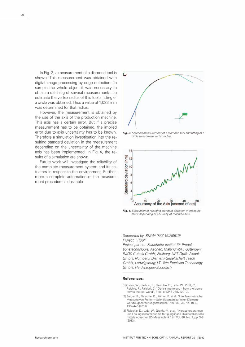
36
In Fig. 3, a measurement of a diamond tool is shown. This measurement was obtained with digital image processing by edge detection. To sample the whole object it was necessary to obtain a stitching of several measurements. To estimate the vertex radius of this tool a fitting of a circle was obtained. Thus a value of 1,023 mm was determined for that radius.
However, the measurement is obtained by the use of the axis of the production machine. This axis has a certain error. But if a precise measurement has to be obtained, the implied error due to axis uncertainty has to be known. Therefore a simulation investigation into the re-sulting standard deviation in the measurement depending on the uncertainty of the machine axis has been implemented. In Fig. 4, the re-sults of a simulation are shown.
Future work will investigate the reliability of the complete measurement system and its ac-tuators in respect to the environment. Further-more a complete automation of the measure-ment procedure is desirable.
Supported by: BMWi (FKZ 16IN0519)Project: “iTool”Project partner: Fraunhofer Institut für Produk-tionstechnologie, Aachen; Mahr GmbH, Göttingen; IMOS Gubela GmbH, Freiburg; UPT-Optik Wodak GmbH, Nürnberg; Diamant-Gesellschaft Tesch GmbH, Ludwigsburg; LT Ultra-Precision Technology GmbH, Herdwangen-Schönach
References:
[1] Osten, W.; Garbusi, E.; Fleischle, D.; Lyda, W.; Pruß, C.; Reichle, R.; Falldorf, C. “Optical metrology – from the labora-tory to the real world”, Proc. of SPIE 7387 (2010).
[2] Berger, R.; Fleischle, D.; Körner, K. et al. “Interferometrische Messung von Freiform-Schneidkanten auf einer Diamant-werkzeugbearbeitungsmaschine”, tm. Vol. 78, No. 10, S. 439–446 (2011).
[3] Fleischle, D.; Lyda, W.; Gronle, M. et al. “Herausforderungen und Lösungsansätze für die fertigungsnahe Qualitätskontrolle mittels optischer 3D-Messtechnik” tm Vol. 80, No. 1, pp. 3-8 (2013).
Fig. 3: Stitched measurement of a diamond tool and fitting of a circle to estimate vertex radius.
Fig. 4: Simulation of resulting standard deviation in measure-ment depending of accuracy of machine axis.
Research projects INSTITUT FÜR TECHNISCHE OPTIK, ANNUAL REPORT 2011/2012

37
SLM-based vibrometry ................................................................................................. 38 Supported by: BMBF (13N9339)Project: “Holovib – LC-basierte holografische Strahlsteuerung für flexible Vibrometriesysteme”
Optimizing the diffraction efficiency of SLMs:Jones matrix simulation model and time dependent variations .................................... 40 Supported by: DFG (OS 111/23-2)Project: “Untersuchung zur Ansteuerung pixelierter räumlicher Lichtmodulatoren für die Rekonstruktion digitaler Hologramme II”
Fast detection of wavefront disturbance: Holographic modal wavefront sensor ...........................................................................41 Supported by: DFG (OS 111/29-1)Project: “Systemanalyse und Methoden zum Reglerentwurf für verformbare Sekundärspiegel in der Adaptiven Optik”
Programmable microscopy ........................................................................................... 42 Supported by: DFG (HA 3490/2-1)Project: “Programmable Microscope Techniques based on light modulator aided Pupil Manipulation”
A systematic method for the description of optical inspection tasks ........................... 44
Active Optical Systems and Computational Imaging
INSTITUT FÜR TECHNISCHE OPTIK, ANNUAL REPORT 2011/2012 Research projects

38
Within the BMBF project “Holovib” dif-ferent uses of spatial light modulators for heterodyne-based vibrometry have been examined. The elements are used for beam-forming and beam-scanning. The main focus are a) single-point scanning systems, b) dy-namic multipoint systems, and c) methods for avoiding speckle-induced loss of signal. In the period 2011/2012, especially multi-point vibrometry has been investigated. In cooperation with Polytec, a 14-channel sys-tem has been developed (5 MHz heterodyne frequency, = 532 nm). The central ele-ment is a spatial phase modulator (Holoeye Pluto, 1920 x 1080 pixels, 8 µm pixel pitch, 2π phase modulation). The system uses one of the two halves of the light modulator for displaying a Fourier hologram, which leads to the generation of the measurement points on the object. The detection hologram is writ-ten into the other half of the modulator. By this detection hologram, the light reflected/scattered at the object is directed onto indi-vidual photodetectors. There, the superposi-tion with the reference leads to the measure-ment signal. The design has been done in Zemax (light scattering analysis in ASAP) and resulted in a diffraction-limited performance over the whole object field.
One of the main challenges of such an ap-proach is to avoid that one of the unwanted diffraction orders might also fall onto a detec-tor. When using a complex superposition of the sub-holograms (advantage: achieving a large aperture and thus a small measure-ment spot), a lot of unwanted orders will be present (approximately 10,000 to 100,000 orders). With an appropriate combination of hologram optimization and mechanical aper-tures it is possible to avoid that they cause a signal at the detector.
The main problem of all techniques for multipoint vibrometry is the loss of signal when working on scattering surfaces. Even when using shot noise limited electrons and strong coherent gain the signal to noise ratio is strongly reduced. Regardless of the con-cept, when using N channels a decrease in signal intensity by 1/N2 will result. This prob-lem can be partially offset by an increased laser intensity or an increase of the total pupil
SLM-based vibrometry
T. Haist, C. Lingel, M. Warber, W. Osten
area. Unfortunately, the pupil area is finally limited in the spatial light modulator-based system by the number of pixels in combina-tion with the desired maximum object field (area and maximum deflection angle are cou-pled via a telescope).
As a result, the experimental setup in the project (20 mW laser source) currently is limited to a simultaneous measurement of 4 channels. Within an additional static sys-tem we could improve on this by increasing the total aperture. This comes at the cost of losing the programmability of the positions of the measurement spots. The measure-ment positions are realized by purely manual means. Appropriate static holograms for col-limation and beam splitting have been opti-mized, manufactured and characterized.
For the optimization of speckle-induced signal reduction, an OKO 37 channel mem-brane mirror has been characterized and a suitable control software in C++ has been implemented. Based on a phase-shifting Twyman-Green interferometer, influence functions of the mirror have been measured. A reconstruction matrix has been computed, which directly allows a control of the mir-ror using Zernike coefficients. The system has been used by the University of Wup-pertal (Lehrstuhl für Automatisierungstech-nik/ Regelungstechnik, Prof. Tibken) for the realization of optimization algorithms. The determination of the best suited modes for controlling the mirror was determined at ITO by simulation of corresponding corrections.
Fig. 1: Student when aligning the SLM-based multi-point vi-brometry system.
Research projects INSTITUT FÜR TECHNISCHE OPTIK, ANNUAL REPORT 2011/2012

39
Supported by: BMBF (13N9339)Project: “Holovib – LC-basierte holografische Strahl-steuerung für flexible Vibrometriesysteme”
References:
[1] Haist, T.; Lingel, C.; Osten, W.; Rembe, C.; Winter, M.; Giesen, M. “SLM-based Multipoint Vibrometry,” in Optical Sensors, OSA Technical Digest 2012, paper SM2F.1, (2012).
[2] Haist, T.; Tarbeyevskaya, A.; Warber, M.; Osten, W.; Rembe, C.; Ludwig, M.; Stork, W. “SLM-based multipoint vibrometry”, Proceedings of SPIE Vol. 8082, 80821V, (2011).
[3] Haist, T.; Lingel, C.; Osten, W.; Winter, M.; Giessen, M.; Rem-be, C. “A 14-channel multipoint vibrometry system using dy-namic holography”, Proc. SPIE 8494, 849406, (2012).
[4] Haist, T.; Lingel, C.; Osten, W.; Winter, M.; Giessen, Ritter, F.; Rembe, C. „Advanced multipoint vibrometry using spatial light modulators“, AIP Conf. Proc. 1457, 234-241, (2012).
Fig. 2: Setup for multipoint vibrometry using programmable object positions.
INSTITUT FÜR TECHNISCHE OPTIK, ANNUAL REPORT 2011/2012 Research projects

40
The aim of the DFG Project “Examination of pixelated spatial light modulators for the re-construction of digital holograms II” was to characterize the so called fringing field effect and to improve the diffraction efficiency of spatial light modulators (SLM) by taking the measurement results into account.
To achieve this we first measured the Jones matrices with subpixel resolution us-ing two optical setups. The first one is shown in Fig. 1 and is used to measure the phaser-educed Jones matrices. It consists of two lenses f1 and f2 which image the magnified SLM onto the camera. Using different config-urations of the two polarizers and the quarter wave plate we recorded 15 different intensity distributions. After comparing the measured intensities with 15 simulated intensities and running a simulated annealing optimization we obtain the phaser-educed Jones matri-ces of the SLM with subpixel resolution. By an interferometric setup it was possible to measure the dynamic phase and therefore to complete the Jones matrices.
Using different subpixel Jones matrices from many different gray value steps as a lookup-table, it was possible to simulate the fringing field effect of blazed gratings and cal-culate the diffraction efficiencies. By chang-ing the gamma curve of the SLM it was pos-sible to optimize the diffraction efficiencies in the simulation, applying a simulated annealing algorithm, for different blazed grating periods (3 pixel to 10 pixel) for horizontal and vertical directions. To prove the results the diffraction efficiency of the real SLM was measured and it turned out that there was an improvement of the efficiency (for some cases about 10%) for the small periods but not for the large. This is due to the fact, that the fringing field effect for larger periods does not have such a significant influence because the step size between the pixel values is smaller.
It also turned out that there is a strong de-pendence of the diffraction efficiency on the pulse width modulation (PWM) of the SLM. Fig. 2 shows the time dependent diffraction efficiency of a 4 pixel blazed grating realized with different PWM types, measured with a photodiode. It clearly shows the complex be-havior of the diffraction efficiency of the SLM.
Optimizing the diffraction efficiency of SLMs:Jones matrix simulation model and time dependent variations
C. Lingel, M. Hasler, T. Haist, W. Osten
Supported by: DFG (OS 111/23-2)Project: “Untersuchung zur Ansteuerung pixelierter räumlicher Lichtmodulatoren für die Rekonstruktion digitaler Hologramme II”
References:
[1] Lingel, C.; Haist, T.; Osten, W. “Examination and optimizing of a liquid crystal display used as spatial light modulator con-cerning the fringing field effect”, Proc. SPIE 8490, Laser Beam Shaping XIII, 84900H (October 15, 2012).
[2] Lingel, C.; Thiel, C.; Haist, T.; Osten, W. “Fringing Field Ef-fect and the measurement of the subpixel jones matrices of an LCD”, Proceedings der DGaO 2012, Eindhoven.
Fig. 1: Optical Setup for measuring the phasereduced Jones matrices of the SLM with subpixel resolution.
Fig. 2: Time dependent diffraction efficiency (Voltage of Photo-diode) of a blazed grating (4 pixel period) with different PWM methods (given by the constructor of the SLM).
Research projects INSTITUT FÜR TECHNISCHE OPTIK, ANNUAL REPORT 2011/2012

41
The rapid measurement of wavefronts is necessary for many tasks in the field of adap-tive optics. Usually Shack-Hartmann sensors are employed. Unfortunately, at high speed such approaches typically become expen-sive due to sampling and data processing.
An interesting alternative is to use modal wavefront sensors. In order to detect a cer-tain aberration mode a hologram is used, which encodes the corresponding mode. Il-lumination of the hologram with the mode leads to two spatially separated spots and by measuring the intensity of these spots using photodiodes one can determine the strength of the mode (see Fig. 1). For the detection of multiple modes, a multiplex hologram is employed and the detectors are placed at the pre-designed positions for the evaluation of each mode (see Fig. 2). Since a thin hologram is used to deflect the light, this sensor is lim-ited to applications where the light source is monochromatic. For small aberrations, the accuracy of the wavefront determination is very good. The more modes to be measured are contained in the wavefront, the greater the crosstalk between the individual holo-grams and therefore the less accurate are the results of the wavefront determination.
If appropriate design parameters are em-ployed and the whole sensor is used within an iterative correction loop, within a few it-erations a sufficiently good optimization of the wavefront can be achieved. Within the project appropriate sensors were optimized for the detection of atmospheric aberrations and tested in a closed-loop adaptive optics system. We also plan to investigate the new concepts by combining the traditional Shack-Hartmann sensing and modal wavefront sensing. The aim is to realize a fast but inex-pensive wavefront sensor concept in which different functions are encoded in a single hologram.
The work is performed in close coopera-tion with the Institute for System Dynamics (ISYS, Prof. Sawodny). A holistic view of the overall correction, consisting of wavefront measurement, control and wavefront modu-lation, and we hope to improve the perfor-mance of an adaptive optics system.
Fast detection of wavefront disturbance:Holographic modal wavefront sensor
S. Dong, T. Haist, W. Osten
Supported by: DFG (OS 111/29-1)Project: “Systemanalyse und Methoden zum Reglerentwurf für verformbare Sekundärspiegel in der Adaptiven Optik”
References:
[1] Dong, S.; Haist, T.; Osten, W.; Ruppel, T.; Sawodny, O. „Response analysis and experimen-tal results of holography-based modal Zernike wavefront sensor“, Proc. SPIE 8165, 816506 (2011).
[2] Dong, S.; Haist, T.; Osten, W.; Ruppel, T.; Sawodny, O. „Response analysis of holography-based modal wavefront sensor“, Appl. Opt. 51, 1318-1327(2012).
Fig. 1: Basic principle of measuring magnitude of single Zernike mode in HMWS.
Fig. 2: Binary-phase hologram of the HMWS (a) (transmission values: white 1, black -1, grey 0) and its diffraction pat-tern (b).
INSTITUT FÜR TECHNISCHE OPTIK, ANNUAL REPORT 2011/2012 Research projects
(a) (b)

42
In the course of the DFG-project “Propu-pil” we investigate the opportunities of com-puta-tional microscopy. Through introduction of a spatial light modulator (a Holoeye Pluto LCD with Full-HD resolution) into the imag-ing branch of a microscopic setup, we were able to create improved flexibility and user-friendliness in the microscope’s capabilities. By placing the LCD in a plane conjugate to the Fourier plane it is possible to apply digital Fourier filters. These filters can be used to realize classical microscope techniques such as Zernike phase contrast or differential inter-ference contrast, which conventionally are achieved by partly intricate alterations in the respective microscope setups, by displaying complex patterns on the LCD.
The flexibility of the LCD also allows for superposition of different patterns, virtu-ally allowing to crossbreed microscope tech-niques, whose combination in a traditional physical setup would be laborious if possible at all.
Additionally the LCD enables the micro-scope to correct for optical aberrations that might be introduced into the setup by any means. These adaptions allow the setup to achieve diffraction limited imaging.
Another application can be achieved by di-verting the light falling onto the display onto two different images in the camera plane. Since the LCD-plane is an image plane of the entrance pupil, we are able to interpret the directional differences in the twin images to retrieve 3d information for stereovision on the object.
In order to increase the capabilities of the microscope, an additional illumination was in-stalled that can be controlled in the same way as for the imaging. To achieve this, the LCD is divided into two halves and while one half is programmed to control the imaging pathway, the other is employed to use computergen-erated holograms for coherent illumination. This is possible without any substantial loss due to the wide 16:9 format of the display.
Additionally, this allows for the implemen-tation of a confocal measurement technique. Through simultaneous defocusing in both ho-lograms a scanning focus spot on an object can be achieved and imaged properly.
Programmable microscopy
M. Hasler, M. Warber, T. Haist
Some results are shown in figure 1, dis-playing a number of images recorded of the same object, with different microscope tech-niques.
Fig. 1: A number of images of a CGH taken with different mi-croscopy techniques: a) Brightfield b) Darkfield c) V-DIC d) W-DIC e) V-DIC+Phaseshift f) Zernike.
Research projects INSTITUT FÜR TECHNISCHE OPTIK, ANNUAL REPORT 2011/2012

43
INSTITUT FÜR TECHNISCHE OPTIK, ANNUAL REPORT 2011/2012 Research projects
Supported by: DFG (HA 3490/2-1)Project: “Programmable Microscope Techniques based on light modulator aided Pupil Manipulation”
References:
[1] Hasler, M.; Haist, T.; Osten, W. „Stereo vision in spatial-light-modulator based microscopy“, Optics Letters 37, 2238-2240 (2012).
[2] Hasler, M.; Haist, T.; Osten, W. „SLM-based microscopy“, Proc. SPIE 8430, 84300V (2012).
[3] Warber, M.; Haist, T.; Hasler, M.; Osten, W. „Vertical differen-tial interference contrast’’, Optical Engineering 51(1), (2011).
[4] Warber, M.; Hasler, M.; Haist, T.; Osten, W. „Vertical Differ-ential Interference Contrast using SLMs,” Proc. SPIE 8086, 80861E (2011).
Fig. 2: The schematic design of the computational microscope.
Fig. 3: An image of the microscope with simultaneous illumination.

44
Research projects INSTITUT FÜR TECHNISCHE OPTIK, ANNUAL REPORT 2011/2012
Within the last years the increase of com-petition and rapid industrialization of automo-tive industry caused a higher requirement of automation production systems. In this aspect, the visual quality control systems take their place in order to make an impor-tant contribution for flexible production sys-tems. Nevertheless, the diversity of optical inspection tasks with different challenges, the increased complexity of processes with short production cycles, the rapid develop-ment of visual inspection systems in order to be competitive, specimen of different ma-terials, forms, manufacturing processes and functional requirements and the inspection fea-tures with a wide range of application and function area are not conducive to find-ing solutions for such tasks, especially for automated surface inspection.
In this work, a systematic method for the description of specific and complicated vi-sual inspection tasks has been developed. The method is designed according to a hier-archical structure: the classification of the in-
A systematic method for the description of optical inspection tasks
V. Erdogan, W. Osten
spection object, the inspection task, relevant features and the selection of the inspection sequence. Especially, the inspection fea-tures, here the surface defects, are in the focus of this work and plays hereby the key role. The description of surface defects is based on two main parts. In the first part, the defects will be characterized with respect to certain criteria like occurrence, form and ap-pearance. Based on this, in the second part, a mathematical description of the defects takes place in form of the classification in several steps.
For the verification of the developed meth-od diverse experiments on the technical sur-faces of a die-cast aluminium part in the au-tomotive industry have been conducted. The goal has been the creation of a detailed and documented catalogue of possible kinds of defects on the technical surfaces of the pow-ertrain. It includes 21 defect types with be-tween 5 and 10 pieces for each defect type. Some examples are shown in Fig. 1.
Fig. 1: Examples of surface defects for basic description.

45
Influence of line edge roughness on scatter signatures for CD-metrology .................. 46 Supported by: European Community FP7Grant agreement no. 215723
Model-based reconstruction of periodic sub-wavelength structures by white light interference Fourier scatterometry ........................................................ 47 Supported by: DFG (SPP 1327) Project: “Optically Generated sub-100-nm Structures for Biomedical and Technical Applications”
Design of microlenses using plasmonic stacks ............................................................ 49 Supported by: Federal Ministry of Education and Research.Project: “BMBF-Project UMABASA”
Improved speckle simulator for rough surfaces using surface integral equations .................................................................................. 50
Reconstruction of dynamical perturbations in optical systems ......................................51 Supported by: DFG (EXC 310/1) “Cluster of Excellence in Simulation Technology”
Sub-wavelength imaging with metallic meander structures ........................................ 52 Supported by: Baden-Württemberg StiftungProject: “Optical Metamaterials for process control environments (OPTIM)”
Polarization scrambling with plasmonicmeander-type metamaterials for space applications .................................................... 54 Supported by: ESTEC 4200022943/10/NL/AFProject: “Metamaterials for Optical and Photonic Applications in Space”
Depth-sensitive fluorescence measurements for diagnostic investigations ................. 55 Supported by: Baden-Württemberg StiftungProject: “Tiefenaufgelöste Fluoreszenzdetektion für die medizinische Diagnostik”
High Resolution Metrology and Simulation
INSTITUT FÜR TECHNISCHE OPTIK, ANNUAL REPORT 2011/2012 Research projects
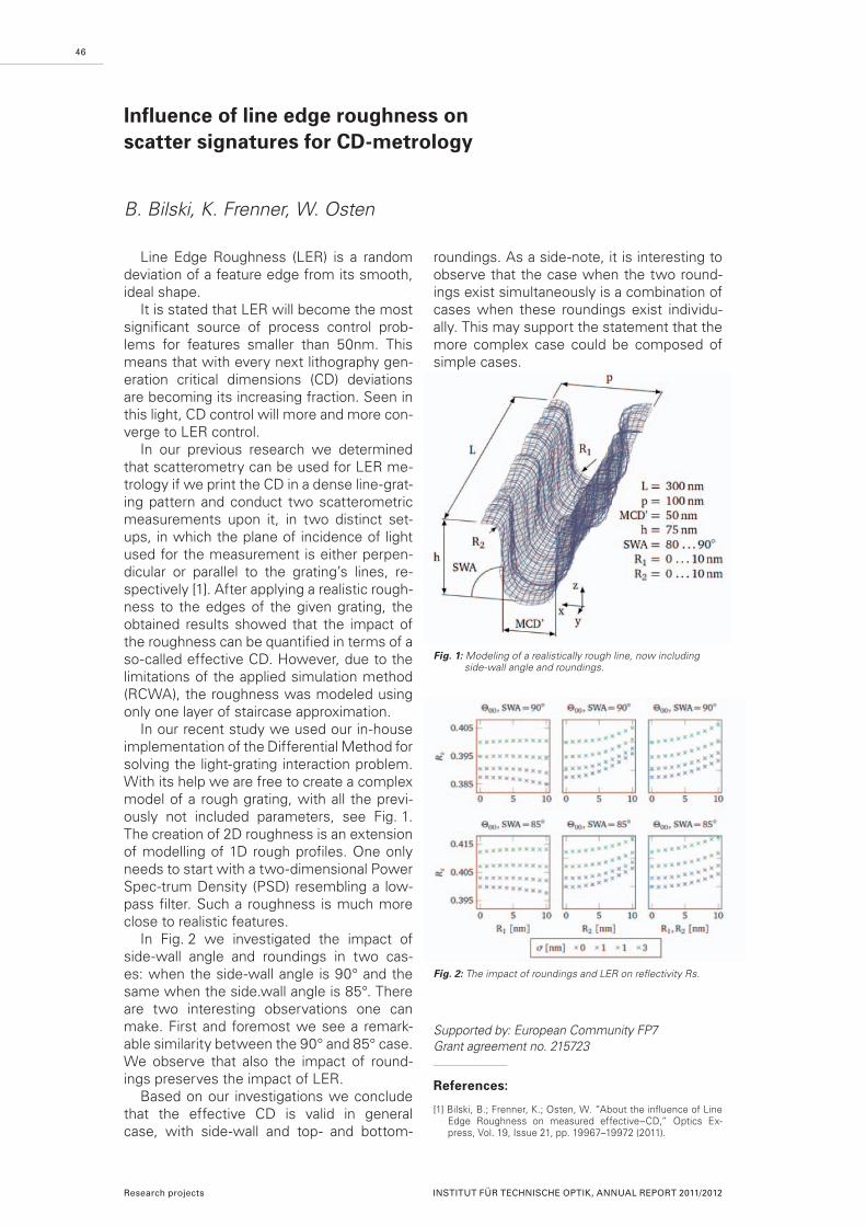
Line Edge Roughness (LER) is a random deviation of a feature edge from its smooth, ideal shape.
It is stated that LER will become the most significant source of process control prob-lems for features smaller than 50nm. This means that with every next lithography gen-eration critical dimensions (CD) deviations are becoming its increasing fraction. Seen in this light, CD control will more and more con-verge to LER control.
In our previous research we determined that scatterometry can be used for LER me-trology if we print the CD in a dense line-grat-ing pattern and conduct two scatterometric measurements upon it, in two distinct set-ups, in which the plane of incidence of light used for the measurement is either perpen-dicular or parallel to the grating’s lines, re-spectively [1]. After applying a realistic rough-ness to the edges of the given grating, the obtained results showed that the impact of the roughness can be quantified in terms of a so-called effective CD. However, due to the limitations of the applied simulation method (RCWA), the roughness was modeled using only one layer of staircase approximation.
In our recent study we used our in-house implementation of the Differential Method for solving the light-grating interaction problem. With its help we are free to create a complex model of a rough grating, with all the previ-ously not included parameters, see Fig. 1. The creation of 2D roughness is an extension of modelling of 1D rough profiles. One only needs to start with a two-dimensional Power Spec-trum Density (PSD) resembling a low-pass filter. Such a roughness is much more close to realistic features.
In Fig. 2 we investigated the impact of side-wall angle and roundings in two cas-es: when the side-wall angle is 90° and the same when the side.wall angle is 85°. There are two interesting observations one can make. First and foremost we see a remark-able similarity between the 90° and 85° case. We observe that also the impact of round-ings preserves the impact of LER.
Based on our investigations we conclude that the effective CD is valid in general case, with side-wall and top- and bottom-
roundings. As a side-note, it is interesting to observe that the case when the two round-ings exist simultaneously is a combination of cases when these roundings exist individu-ally. This may support the statement that the more complex case could be composed of simple cases.
Supported by: European Community FP7Grant agreement no. 215723
References:
[1] Bilski, B.; Frenner, K.; Osten, W. “About the influence of Line Edge Roughness on measured effective–CD,” Optics Ex-press, Vol. 19, Issue 21, pp. 19967–19972 (2011).
46
Influence of line edge roughness on scatter signatures for CD-metrology
B. Bilski, K. Frenner, W. Osten
Fig. 1: Modeling of a realistically rough line, now including side-wall angle and roundings.
Fig. 2: The impact of roundings and LER on reflectivity Rs.
Research projects INSTITUT FÜR TECHNISCHE OPTIK, ANNUAL REPORT 2011/2012

The white light interference Fourier scat-terometry setup is based on a typical Fourier scatterometer. Instead of monochromatic il-lumination, the sample is illuminated using a broadband white light source. Additionally, a reference branch including a reference mirror for white light interference is introduced. The interfering pupil images from the object and reference branch are imaged with a Bertrand lens on a CCD camera. The schematic setup is depicted in Fig. 1. For reconstruction of the structure profile, a comparison between meas-ured and simulated pupil images for each z-position of the scanned reference mirror is performed until the best match is found.
As part of the DFG priority program SPP 1327 “Optically Generated sub-100-nm Structures
for Biomedical and Technical Applications” we already presented in the ITO annual report 2009–2010 a simulation based analysis com-paring the sensitivity of the white light Fourier scatterometry method to other scatteromet-ric configurations. To verify the promising re-sults obtained from simulation we now built up the experimental setup and compared the resulting structure reconstruction of a sub-lambda silicon line grating to measurements with an atomic force microscope (AFM) as well as with a scanning electron microscope (SEM).
The comparison between measured and simulated pupil images can be found in Fig. 2 Performing a library search the structure pa-rameters can be reconstructed. The values obtained are compared to the AFM and SEM
47
Model-based reconstruction of periodic sub-wavelength structures by white light interference Fourier scatterometry
V. Ferreras Paz, S. Peterhänsel, K. Frenner, W. Osten
Fig. 2: Measured and simulated pupil images for a z-scan of the reference mirror for the silicon grating CD=200 nm.
Fig. 1: Schematic overview of experimental setup.
INSTITUT FÜR TECHNISCHE OPTIK, ANNUAL REPORT 2011/2012 Research projects

reference measurements. The results can be found in Tab. 1. The reconstructed values are in good agreement, although the height is at the upper limit. One should keep in mind that scatterometry always integrates over the complete illuminated area (multiple peri-ods of the line grating), while SEM and AFM always yield results at the chosen measure-ment site. Especially when the structure suf-fers from line edge roughness (LER), there can be differences in the values obtained by direct measurement methods compared with the integrated values obtained from our model-based measurement technique, which at the moment does not take into ac-count LER effects.
The method is well suited for the model-based profile reconstruction (Fig. 3) of peri-odic line gratings of silicon, which are often used in the semiconductor industry. The measurements performed were reproduced satisfactorily by simulations. A library search inside the precomputed library identifies the best agreement and gives us the possibility to easily obtain the profile parameters of the analyzed structure.
Supported by: DFG (SPP 1327) Project: “Optically Generated sub-100-nm Structures for Biomedical and Technical Applications” (http://www.spp1327.de)Cooperation with: Nanotechnology Department at the Laser Zentrum Hannover e.V.
References:
[1] Ferreras Paz, V.; Peterhansel, S.; Frenner, K.; Osten, W.; Ov-sianikov, A.; Obata, K.; Chichkov, B. „Depth sensitive Fouri-er-Scatterometry for the characterization of sub-100 nm pe-riodic structures” Proceedings of SPIE (2011) Vol. 8083, p. 80830M–80830M–9. doi:10.1117/12.889439.
[2] Ferreras Paz, V.; Peterhänsel, S.; Frenner, K.; Osten, W. „Solv-ing the inverse grating problem by white light interference Fou-rier scatterometry” (2012) Light: Science & Applications, 1(11), e36. doi:10.1038/lsa.2012.36.
48
Research projects INSTITUT FÜR TECHNISCHE OPTIK, ANNUAL REPORT 2011/2012
Parameter Value [SEM]
Value [AFM]
Value [Reconstr.]
Mid-CD [nm] 182 ± 7 – 182 nm
Pitch [nm] 400 ± 2 400 ± 2 nm –
Height [nm] 76 ± 9 72 ± 7 nm 85 nm
SWA [°] 77 ± 3 – 77.5 °
Fig. 3: Schematic flowchart of the reconstruction strategy in general model-based metrology.
Tab. 1: Profile parameter ranges for the silicon grating (CD=200nm) measured with AFM, SEM and the recon-structed values obtained from the white light Fourier Scatterometry measurement.

49
Plasmonics is a flourishing new field of science and technology due to its capability to confine light into a subwavelength volume, which induces strong light matter interactions at nanometer scales. Novel optical elements for light harvesting, plasmonic antennas, su-per-lenses and resonators have been devel-oped in the last decade [1]. In the framework of a project with Bundesdruckerei GmbH, a novel type of plasmonic microlens using metal/dielectric stacks has been designed and simulated. The developed structure is of great importance for security elements, laser cavity reflectors or CD/DVD read/write heads with controlled focus size and length [2].
Fig. 1 shows a schematic of a periodic plasmonic structure embedded in polycar-bonate (PC) with two unit cells. The metal is Silver and its dielectric constant is described by a Drude model. The dielectric is assumed to be PC having a refractive index of 1.58 at a wavelength of 630 nm. Our inhouse devel-oped software package Microsim based on Rigorous Coupled Wave Analysis was used to simulate the structure. To obtain a parabol-ic phase front of the reflected beam, we treat the stacks as an effective medium and its ef-fective index was approximated using the fol-lowing equation, which is only valid when the thickness of the layers is much smaller than the wavelength:
, (1)
in which, εm and εd is the permittivity of metal and dielectric, respectively, and h is the filling factor of the dielectric determined by , in which d(m, d) is the corresponding thickness of the metal or dielectric.
The results of a plasmonic lens de-signed for 630 nm wavelength are shown in Fig. 2. To obtain a reflected focused field at z = -150 µm (the top surface of the structure locates at z = 0 µm), a parabolic wavefront of the reflected waves is desired. To achieve this, three pair of Ag/PC layers with thick-nesses of 30/107 nm and widths of 25, 20, and 15 µm from bottom to top as shown in Fig. 1 were derived based on Eq.(1). Fig. 2(a) shows the intensity of the electric field above the stacks under the illumination of a p-po-
Design of microlenses using plasmonic stacks
L. Fu, K. Frenner, W. Osten
larized plane wave. It was also found that the focusing characteristics was kept under a tilted illumination of 30° and was robust in a larger wavelength and structure parameter range. Future work will focus on developing and fabricating plasmonic lens with a stron-ger focus capability and smaller size.
This work was cooperated with Bundesdruckerei GmbH in the framework of the BMBF-Project UM-ABASA [3]. We thank the support from the Federal Ministry of Education and Research.
References:
[1] Schuller, J.A.; Barnard, E.S.; Cai, W.; Jun, Y.C.; White, J.S.; Brongersma, M.L. “Plasmonics for extreme light concentra-tion and manipulation,” Nature Materials 9, p. 193-204, 2010.
[2] Fattal, D.; Li, J.; Peng, Z.; Fiorentino, M.; Beausoleil, R.G. “Flat dielectric grating reflectors with focusing abilities,” Nature Pho-tonics 4, p. 466-470, 2010.
[3] www.umabasa.de
Fig. 1: Plasmonic Ag/PC stacks as a microlens based on the effective medium theory. The metal is Ag described by a Drude model and the dielectric is Polycarbonate hav-ing a refractive index of 1.58 at 630 nm.
Fig. 2: (a) Focus demonstration of three pairs of Ag/PC layers with thicknesses of 30/107 nm embedded in PC illuminated with a p-polarized plane wave at a wavelength of 630 nm. The width of the layers from bottom to top is 25, 20 and 15 µm, respectively. (b) Intensity distribution at z = -150 µm (the black curve), phase distribution (the red curve) at z = 0 µm, and the designed phase distribution using Eq.(1).
INSTITUT FÜR TECHNISCHE OPTIK, ANNUAL REPORT 2011/2012 Research projects
(a) (b)

Any real surfaces, both those occurring naturally, and those fabricated artificially, are rough to some degree. It is of great interest and importance to know how this roughness affects physical properties of a surface. The scattering of electromagnetic waves from rough surfaces has been studied actively for more than a century now. More than thirty analytical approximation methods have been developed [1], among which the often used ones are small amplitude perturbation theo-ry, Rayleigh-Rice and the Beckmann-Kirch-hoff theory. In the last two decades, great advances in analytic approaches have been made by incorporating multiple scattering ef-fects into the approaches. However, analytic models are all valid only in some specific ap-plication ranges [1].
In order to gain a fundamental understand-ing of how light interacts with a broad vari-ety of rough surfaces, we aim to develop a rigorous numerical simulator for penetrable metals with a surface roughness in a large variation range. For this aim the full Maxwell equations have to be solved and surface integral equations with boundary element method were most often used. Based on Stratton-Chu’s formulation and the associ-ated boundary conditions on the tangential field components, a generalized formulation is obtained (PMCHW [2]):
, (1)
, (2)
in which M and J are equivalent magnetic and electric surface currents induced by the incident fields Einc(r) and Hinc(r), respectively. K(1, 2) and L(1, 2) are linear integrodifferential op-erators and η1 and η2 are the impedances of the two media above and below the surface.
To solve the two coupled equations, the rough surface, which is modeled using Monte Carlo methods, is discretized using isoparametric elements (boundary element method). In this work, the element takes a curvilinear quadrilateral shape as shown in Fig. 1, which is more accurate compared to planar elements [3]. The approximated field
in each element is calculated through a linear combination of the 10 edges:
, (1)
in which Ni = fi vi is vector element function along each edge, vi is the gradient of η or of the edge i, and SHi denotes the line-integral of J along the edge i (i = 1, ..., 10) [3]. A simi-lar equation exits for M.
By using Galerkin method, the integra-tion equations can be transformed into linear matrix equations. Once the unknown coeffi-cients fi for the effective current density in each element are solved, the E (or H) field everywhere in space can be calculated corre-spondingly [2]. Especially, one of the advan-tages with this method is that both near and far field can be calculated accurately.
Fast multiple method combined with an iterative solver can accelerate the solution of the matrix equations.
50
Improved speckle simulator for rough surfaces using surface integral equations
L. Fu, K. Frenner, W. Osten
Fig. 1: Numbering scheme of the edges of a curvilinear quadri-lateral shape element.
References:
[1] Elfouhaily, T.M.; Gu´erin, C.-A. “A critical survey of approxi-mate scattering wave theories from random rough surfaces,” Waves of Random Media 14, p. R1–R40, 2004.
[2] Medgyesi-Mischang, L.N.; Putnam, J. M.; Gedera, M.B. “Generalized method of moments for three-dimensional pen-etrable scatterers,” J. Opt. Soc. Am. A 11, p. 1383-1398, 1994.
[3] Huber, C.J.; Rieger, W.; Haas, M.; Rucker, W.M. “A boundary element formulation using higher order Curvilinear edge ele-ments,” IEEE Transactions on Magnetics 34, p. 2441-2444, 1998.
Research projects INSTITUT FÜR TECHNISCHE OPTIK, ANNUAL REPORT 2011/2012

High-performance optics pose strict limita-tions on errors present in the system. Exter-nal mechanical influences can induce struc-tural vibrations in such a system, causing the optical components inside the objective to deviate from their designated positions. This can have an impact on the imaging perfor-mance, leading to blurred images or broad-ened structures in lithography processes.
A method to detect and predict the motion of the components of such an optical system by means of opto-mechanical simulation in combination inverse problem theory has been demonstrated. Such a method is the first step towards a control loop that corrects the lens positions with mechanical manipulators.
On the optical side of the simulation, ray-tracing is used for the generation of wave-front data of the system in its current state. A high speed Shack-Hartmann wavefront sensor is therefore implemented to gather the data needed for the reconstruction of the motion. The mechanical properties of the system are simulated using multibody dynamics, where the system is mod-elled as a set of rigid bodies (lenses, mounts, barrel), represented by rigid masses connected by springs that represent the coupling between the individual parts. External excitations cause the objective to vibrate. This motion can be represented by the eigenmodes and eigenfrequencies of the system.
The reconstruction of the system geom-etry as a function of time from the wavefront data is an inverse problem. Tikhonov regu-larization is used in the process in order to achieve accurate reconstruction results. This method relies on a certain amount of a-priori information on the system. The mechanical properties of the system are a great source of such information. It is taken into account by performing the calculation in the coordi-nate system spanned by the eigen-modes of the objective and using information on the spectrum of frequencies present in the cur-rent vibration as a-priori data. The positions of the individual lenses as a function of time is then reconstructed from several frames of the wavefront data and extrapolated to fu-ture timesteps in order to give a prediction on the system behaviour. This can be useful
for applying and controlling countermeasures against the vibrations of the objective or for designing new systems that are less influ-enced by vibrations.
The results of this study have been pub-lished and presented in [1]. The next steps in this project are the extension of the recon-struction process to lens deformations and thermal expansion as well as experimental verification of the results.
51
Reconstruction of dynamical perturbations in optical systems
H. Gilbergs, K. Frenner
Fig. 1: Visualization of the four eigenmodes used to repre-sent system vibrations. The red line is the optical axis. The eigenmodes correspond to the eigenfrequencies f1 = 0.70 s–1 (top left), f2 = 1.10 s–1 (top right), f3 = 2.07 s–1 (bottom left), f4 = 4.11 s–1 (bottom right).
Supported by: DFG (EXC 310/1) “Cluster of Excellence in Simulation Technology”
References:
[1] Gilbergs, H.; Wengert, N.; Frenner, K.; Eberhard, P.; Osten, W. „Reconstruction of dynamical perturbations in optical systems by opto-mechanical simulation methods”, Proc. SPIE 8326, Optical Microlithography XXV, 83262N (February 21, 2012); doi:10.1117/12.916615.
INSTITUT FÜR TECHNISCHE OPTIK, ANNUAL REPORT 2011/2012 Research projects
Fig. 2: Comparison of the quality of the position prediction based on Tikhonov regularization (red) and least squares fit (dashed blue) vs. the number of evaluated timesteps. The results are improved greatly, especially for a lower number of evaluated timesteps. The smallest achiev-able mean position error is for the Tikhonov based method.

In semiconductor manufacturing and nanotechnology, high-resolution metrology is crucial for process and quality control. At this point there are specialized tools avail-able, which enable high-resolution imaging or metrology for individual process steps but no universal device. While demands of the industry have driven technology to the limits, none of the presented solutions is capable to image arbitrary sub-lambda structures direct-ly in a contactless, fast and non-destructive way.
This is where the new research field of metamaterials comes into play. Metamateri-als consist of periodic structures with dimen-sions smaller than the wavelength and can be designed to create particular electromag-netic responses that cannot be found in na-ture. Particularly interesting is the Veselago material, which exhibits a negative refractive index and can be used for superlensing as investigated by Pendry in 2000. Although a simple slab of silver already creates a per-fect image of a sub-wavelength source, the image is still in the near-field and not magni-fied. Hence, all sub-wavelength information will still decay exponentially and vanish in the far field. Our research goal is to design a su-perlens capable of transforming evanescent waves to propagating modes, which then can be imaged via conventional microscopy (see below).
It has been shown that surface plasmon polaritons (SPPs) propagating on the metal/dielectric interfaces of a bulk negative index material (NIM) have a dominant influence on the unique properties of these materials. Consequently, one could replace bulk NIMs by resonantly coupled metallic surfaces that allow the propagation of SPPs.
A metallic meander structure (Fig. 2) is perfectly suited as such a resonant surface due to the tunability of the short range SPP (SRSPP) and long range SPP (LRSPP) fre-quencies by means of geometrical variation.
We have already demonstrated numeri-cally how a stack consisting of two mean-der structures can mimic perfect imaging known from Pendry’s lens. To observe sub-wavelength features in the far-field, however, we extended this principle towards a stack made up of meander structures with varying periodicities. A numerical simulation of this device is shown in Fig. 3.
In the course of the project, we have de-veloped different ways to manufacture single and stacked meander structures preferably with e-beam lithography but also using other techniques such as interference lithography
52
Sub-wavelength imaging with metallic meander structures
P. Schau, L. Fu, K. Frenner, H. Schweizer. H. Giessen, W. Osten
Fig. 1: Basic setup for a superlens attached to a conventional microscope to enable sub-wavelength imaging.
Fig. 2: Meander structure, which enables near-field imaging similar to Pendry’s perfect lens
Research projects INSTITUT FÜR TECHNISCHE OPTIK, ANNUAL REPORT 2011/2012

or focused ion beam milling. We have shown experimentally that the transmission spectra of these meander structures agree well with our numerical simulations. Furthermore, we demonstrated negative refraction occurring in meander structures using dispersion mea-surements and have high hopes to realize a proof of principle superlens in the near future.
53
Fig. 3: Stack consisting of four meander structures that magni-fies two sub-wavelength holes by a factor of 8.
Supported by: Baden-Württemberg StiftungProject: “Optical Metamaterials for process control environments (OPTIM)”In cooperation with: 4th Physics Institute and Research Center SCoPE, Universität Stuttgart
References:
[1] Schau, P.; Frenner, K.; Fu, L.; Schweizer, H.; Osten, W. “Cou-pling between surface plasmons and Fabry-Pérot modes in metallic double meander structures”, Proc. SPIE 7711, p. 77111F, 2010.
[2] Schau, P.; Frenner, K.; Fu, L.; Schweizer, H.; Giessen, H.; Os-ten, W. “Design of high-transmission metallic meander stacks with different grating periodicities for subwavelength-imaging applications”, Optics Express 19, pp. 3627-3636, 2011.
[3] Schweizer, H.; Fu, L.; Hentschel, M.; Weiss, T.; Bauer, C.; Schau, P.; Frenner, K.; Osten, W.; Giessen, H. “Resonant multimeander-metasurfaces: A model system for superlenses and communication devices,” physica status solidi (b) 249, pp. 1415-1421, 2012.
INSTITUT FÜR TECHNISCHE OPTIK, ANNUAL REPORT 2011/2012 Research projects

The polarization state of light is one of the most important properties for many optical applications. However, in some instances, such as earth observation from space, any exhibited polarization of the light is undesir-able and depolarization of the light is critical for a good optical performance of a space-based instrument. One approach towards depolarizers are so called polarization scram-blers or pseudodepolarizers, which divide the incident light beam into a large number of varying and intermixed polarization angles in-stead of truly depolarizing the light. Currently and historically, most pseudodepolarizers in space instruments utilize different arrange-ments of birefringent wedges. Major draw-backs of these designs are their bulkiness, heavy weight and limitation in size due to the anisotropy of the thermal expansion coeffi-cient of birefringent materials.
Especially for space instruments, large-area and low-weight optical elements are desirable. So-called metamaterials could advantageously replace bulky standard op-tical components with thin layers of the same functionality but lower mass and vol-ume. Depolarization effects in metamaterials have been discussed frequently in literature whereas metamaterial pseudodepolarizers have not been investigated yet.
The device proposed by ITO and the 4th Physics Institute is based on metallic mean-der structures (see OPTIM project report), which behave not only like an almost ideal linear polarizer, but also demonstrate a large phase retardation and polarization conversion capability between two orthogonal polariza-tion states. The main idea of our approach consists of meander structures that are spa-tially distributed on a surface. Each meander structure within such a tile is rotated by a ran-dom angle (Fig. 1).
For perpendicularly incident light (θ = 0), we have described the behaviour of a single meander structure using Jones calculus. Be-cause the meander structure itself is not de-polarizing, it is valid to transform the Jones matrix to a Mueller matrix, which is depen-dent on the azimuth angle φ of the incident polarized light. The random orientation and
distribution of the meander tiles effectively averages the azimuth angles and, hence, φ can be integrated from 0 to 2π. Then, within the pass band of the meander structure, the off-diagonal elements of the averaged Muel-ler matrix are zero and the diagonal elements around 0.5 or smaller. This makes the device already a good partial pseudodepolarizer.
To investigate the behaviour for oblique in-cidence, we used our in-house software tool Microsim to calculate the Mueller matrix rig-orously. We found out that we can enhance the depolarization by stacking two meander sheets onto each other. With this scheme we achieve preliminary depolarization rates of >50% linearly polarized light and even 95% for circularly polarized light.
The presented polarization scrambler might be a good alternative to existing approaches and would be especially desirable for space applications due to its low weight and large-scale manufacturability using nano-imprint lithography.
54
Polarization scrambling with plasmonicmeander-type metamaterials for space applications
P. Schau, L. Fu, K. Frenner, H. Schweizer. H. Giessen, W. Osten
Fig. 1: Working principle of the proposed polarization scram-bler consisting of meander-type metamaterials.
Supported by: ESTEC 4200022943/10/NL/AFProject: “Metamaterials for Optical and Photonic Ap-plications in Space”In cooperation with: 4th Physics Institute and Research Center SCoPE, Universität Stuttgart; European Space Research and Technology Ctr., Noordwijk, Nether-lands; cosine Research B.V., Leiden, Netherlands
References:
[1] Schau, P.; Fu, L.; Frenner, K.; Schäferling, M.; Schweizer, H.; Giessen, H.; Venancio, L. M. G.; Osten, W., “Polarization scramblers with plasmonic meander-type metamaterials”, Op-tics Express 20, pp. 22700-22711, 2012.
Research projects INSTITUT FÜR TECHNISCHE OPTIK, ANNUAL REPORT 2011/2012

Optical coherence tomography (OCT) is an important technology for non-invasive, in-vivo medical diagnostics. It enables the high-resolution recording of two-dimensional tomograms or three-dimensional volumes of biological tissue. Two mechanisms help sep-arating the signal from the scattering back-ground. First, reflected or backscattered light from outside the focal spot is suppressed by confocal discrimination. Additionally, the sig-nal modulation is enhanced due to identical optical path lengths of both branches of the white light interferometry setup. Since the OCT relies on the interference between ref-erence light and scattered light, this method cannot be readily extended for fluorescence measurements.
An alternative approach is the confocal fluorescence microscopy, which uses confo-cal microscopy to suppress the fluorescent light from outside the focal spot. Hence, only the fluorescent light in the focal plane, which is three to four magnitudes lower in intensity than the excitation light, is detected. However, the surrounding area is illuminated with full intensity, which might cause photo-bleaching. There are also other promising ap-proaches such as the two-photon excitation microscopy or fluorescence lifetime micros-copy.
However, for depth-sensitive fluores-cence measurements of strongly-scattering samples such as biological tissue but also for technical surfaces, these methods are not well-suited. To enhance fluorescent depth-sensitive measurements, we cooperate with Institut für Lasertechnologien in der Medizin und Meßtechnik (ILM), Ulm and propose a combination of a structured white-light illu-mination and shearing interferometry (Fig. 1).
For this purpose, a structured illumination limits the area of interest on a rough scale. The exact lateral and axial position of the fluorescent molecules is then determined by a shearing interferometer. Using Fourier analysis, the curvature of the incident wave fronts can be calculated via the density and orientation of the interference fringes. Finally, the axial distance can be determined, which corresponds to the exact location of the par-
ticular molecule emitting fluorescence.In a first step towards the realization of the
whole system, we investigate and optimize the structured illumination. In a setup simi-lar to a white-light interferometer, the light from the two branches is obliquely incident and interferes within the strongly scattering sample. Due to the short coherence length of the white light source, the light superpos-es only coherently for the exact same opti-cal path length of both branches. Scattered or reflected light interferes only marginally or not at all. Hence, there is a ‘plane’ or ‘sheet’ within the strongly scattering sample that is illuminated with a higher intensity than the surrounding volume. The shape and intensity of the interferogram making up this plane can be manipulated with the bandwidth of the white light source and the angle of incidence, respectively. To what effect the scattering within the sample influences the measuring process will be investigated numerically by the ILM
55
Depth-sensitive fluorescence measurements for diagnostic investigations
P. Schau, K. Frenner, W. Osten
Fig. 1: Principle setup of the measurement system consisting of the structured white-light illumination part and the shearing interferometer for detection of fluorescent light.
Supported by: Baden-Württemberg StiftungProject: “Tiefenaufgelöste Fluoreszenzdetektion für die medizinische Diagnostik”In cooperation with: Institut für Lasertechnologien in der Medizin und Meßtechnik (ILM), Ulm
INSTITUT FÜR TECHNISCHE OPTIK, ANNUAL REPORT 2011/2012 Research projects

56
Research projects INSTITUT FÜR TECHNISCHE OPTIK, ANNUAL REPORT 2011/2012

57
The Tilted Wave Interferometer (TWI): A quick and flexible approach to measure asphere and freeform surfaces ................... 58 Supported by: BMBF, EU, Baden-Württemberg StiftungProject: “MesoFrei, FKZN 13N10854 and EMRP JRP project IND10”
Micro optical spatial polarization control ....................................................................... 60 Supported by: DFG OS111/35-1Project: part of the DFG priority programme 1337 “active micro optics”
Fabrication of computer generated holograms on rotationally symmetric curved substrates .................................................................... 61 Supported by: BMBF FZK 16SV2309 Project: “Lynkeus”
Cost effective production of diffractive multi-level elements ..................................... 63 Supported by: BMBI (FKZ KF2281402AB2)Project: “Kosteneffiziente Grautonlithografie für diffraktive Multi-Level Elemente”
Fabrication of diffractive and micro-optical elements for external partners ...................................................................................................... 64
Phase errors introduced in CGH by rigorous effects ..................................................... 65 Supported by: DFG (OS111/32-1)Project: “Inverse source and inverse diffraction problems in photonics ”
Interferometry and Diffractive Optics
INSTITUT FÜR TECHNISCHE OPTIK, ANNUAL REPORT 2011/2012 Research projects

Producing precision optics is always con-nected to careful optical testing. With the need for better, smaller and lighter optical systems the use of aspheres and also free-form surfaces has become a necessity. New and improved fabrication technologies have been developed, and with them the need for adequate testing methods. Over the past decades the testing of aspheres and more recently also the testing of freeform surfac-es has developed from the mere feasibility towards more economic solutions. This re-quires flexible solutions without expensive null optics such as computer generated ho-lograms (CGH). Different scanning systems have been proposed that either test the sur-face under test point-wise or patch-wise. However, time sequential scanning leads to comparatively long measurement times. Our goal with the invention of the Tilted Wave In-terferometer (TWI) was to reduce the mea-surement time to a minimum while still main-taining a high degree of flexibility [1].
The basic idea is to illuminate the sur-face under test (SUT) with a set of discrete wave fronts that are tilted with respect to each other. Thus, for any spot on the SUT there is a matching wave front that leads to an interpretable interferogramm patch. This allows in principle to capture the whole SUT in one measurement. For practical rea-sons – to avoid overlapping of the individual patches – only every second wave front in each direction is switched on. So in practice four measurements are taken of the SUT, with different wave fronts switched on (see figure 1). The SUT is not moved at all during measurement.
In the actual implementation, we can mea-sure aspheres with gradient deviations of up to ±10° relative to the best fitting sphere in about half a minute’s time. Since the tilting
angles of the wavefronts cover angles of ±10° in both x and y-direction, the departure from the sphere does not need to be rotationally symmetric but can be an arbitrary freeform.
Figure 3 shows a measurement result of the freeform surface depicted in figure 2.
The measurement shows fine tooling marks on the aluminium surface, illustrating the high lateral resolution of the method.
As with all non-null testing methods a ma-jor topic is calibration. We use a system of polynomials to describe the aberrations of the interferometer. The coefficients of the system are optimized in the calibration pro-cedure such that they can reproduce the re-sults of a series of calibration measurements. The numerical properties of the polynomial
58
The Tilted Wave Interferometer (TWI): A quick and flexible approach to measure asphere and freeform surfaces
G. Baer, C. Pruß, J. Schindler, W. Osten
Fig. 1: Synthetic phasemaps of the four measurement patch distributions when measuring a freeform surface.
Research projects INSTITUT FÜR TECHNISCHE OPTIK, ANNUAL REPORT 2011/2012
Fig. 2: Free form surface (metal) with an astigmatism of about 800 µm.
Fig. 3: Measurement result showing fine tooling marks on the test surface.

59
system play an important role in the overall accuracy of the system and will be further in-vestigated in current projects together with our partners from the PTB (Physikalisch-Technische Bundesanstalt).
As in all interferometric setups the posi-tioning of the surface under test is important, since a) an incorrectly positioned surface might lead to vignetting and b) it adds align-ment errors to the measurement. The TWI with its huge flexibility in terms of aspheric departure offers a unique situation for this problem. Even for a very badly positioned surface under test there will be a signal that helps finding the approximate correct posi-tion. Having reached this with a coarse align-ment that can be automated (see last annual report) quite efficiently [2], the fine alignment could also be done automatically. However, this can be done virtually. We have realized an algorithm capable of estimating the cor-rect position of the surface under test. With the position information, we can determine and subtract the alignment errors. As an ex-ample, figure 4 shows two measurement re-sults of a surface under test that was laterally shifted by 20 µm between the two measure-ments. As can be seen, the algorithm obtains virtually the same measurement result.
The flexibility of the TWI approach is quite high, yet large surfaces beyond 100 mm di-ameter cannot be measured in one shot with our 4 inch interferometer. In the scope of the BMBF-project MesoFrei we currently investi-gating algorithms to extend the flexibility fur-ther with the help of stitching measurements
and an automated setup that was developed by our industrial partner Mahr. In the stitch-ing approach, the surface under test is mea-sured patchwise and the results are stitched together to cover the whole surface.
INSTITUT FÜR TECHNISCHE OPTIK, ANNUAL REPORT 2011/2012 Research projects
We would like to thank the BMBF and the EU for funding parts of this work (projects MesoFrei, FKZN 13N10854 and EMRP JRP project IND10), the Baden-Württemberg Stiftung for financing part of this work in the project Nanofrom. The good cooperation with our project partners Mahr, PTB and IOF is greatly ap-preciated.
References:
[1] Liesener, J.; Garbusi, E.; Pruß, C.; Osten, W. German Patent DE 10 2006 057 606 A1.
[2] Baer, G.; Garbusi, E.; Lyda, W.; Osten, W. “Automated surface positioning for a non-null test interferometer”, Opt. Eng. 49, 095602 (Sep 15, 2010); doi:10.1117/1.3488051.
Fig. 4: Two measurement results with surface under test shifted laterally by +-10 µm.

The scope of this project is the develop-ment of a compact micro optical device for non-pixelated spatial polarisation control.
The device (Fig. 1) is based on a photoad-dressable material (PAM). The birefringence of the PAM is locally modulated due to the intensity of the addressing light. This enables the creation of non pixelated spatial polariza-tion patterns with fewer artefacts compared to devices like spatial light modulators. The change in polarization depends on the po-larization and intensity of the addressing light. The addressing is done with red light (655 nm), the usable wavelengths for polar-ization manipulation lies in the near infrared (NIR).
The micro optical addressing module (Fig. 2) uses VCSELs as light sources and diffractive optical elements (DOE) for beam shaping. Due to the small dimensions of the illumination system, several addressing chan-nels can be realised in one device. By control-ling the current through the VCSELs, differ-ent illumination patterns can be switched or combined.
The system can achieve resolutions up to 250 LP/mm and can induce a birefringence up to Δn 0.1. The switching time between two birefringence patterns is ~1.5 s.
Further work will focus on the enlarge-ment of the addressable area, the integration of the system into a microscope objective, the realisation of a tuneable integrated phase contrast microscope and the combination with a plenoptic camera.
60
Micro optical spatial polarization control
F. Schaal, C. Pruß, W. Osten
Fig. 1: Schematic diagram of the basic setup.
Fig. 2: Micro-optical illumination unit.
Fig. 3: Microscope objective with adjustable phase contrast.
Supported by: DFG OS111/35-1
This project is part of the DFG priority programme 1337 “active micro optics” and is done in collabora-tion with the IHFG (University Stuttgart), University Potsdam and others.
Research projects INSTITUT FÜR TECHNISCHE OPTIK, ANNUAL REPORT 2011/2012

Hybrid optical elements that combine re-fractive and diffractive functionality are ver-satile components for all kinds of applications in imaging or metrology. In the past those el-ements were composed of a flat diffractive and a curved refractive surface. Fusing both functions in a single surface will enhance the capabilities of these optical components further. The fabrication of such precision elements is a challenge since most micro structuring tools are limited to flat surfaces. The growing interest in structuring non-flat surfaces arises in the increasing number of systems designed for this purpose [1,2]. At the ITO a powerful lithography scheme for the fabrication of high accuracy diffractive structures on rotationally symmetric curved substrates was established. The lithography tool was developed on the basis of the cir-cular laser writing system CLWS300 [3] and allows for the fabrication of binary and grey scale structures on surfaces with slope an-gles of more than 15°.
Working with polar coordinates, the writ-ing system is optimized for the fabrication of rotationally symmetric structures such as Fresnel Zone Plates. Positioning of the writ-ing spot is realized by a rotating air bearing spindle that holds the substrate and a linear air bearing stage which addresses the ra-dial coordinate on the substrate. Writing on curved surfaces implies that the writing head is able to follow the substrate topography. For this, we integrated a linear air bearing stage with small guiding errors and highly re-peatable motion. The stage is mounted col-linear to the angular axis, extending the polar coordinates to a cylinder coordinate system.
Figure 1 shows a schematic of the writing arrangement. Except for the rotating spindle all positioning is performed by linear stages. Tracking of the substrate topography is ac-complished by continuously adjusting the height of the writing head according to the substrate surface sag, thus keeping the sur-face in the focal plane of the micro-scope objective. In order to account for fast autofo-cus response and wide range surface track-ing, positioning of the focussing objective is realized by a hybrid approach combining a
piezo actuator and a linear air bearing stage. Working in cylinder coordinates implies that the writing and autofocus beams are not per-pendicular to the substrate surface when the substrate is curved. We therefore developed and integrated a novel auto focus approach that accounts for the challenge of focusing on tilted surfaces.
The writing system has proven to be ca-pable of structuring rotational symmetric el-ements with surface slope angles of more than 15°.
Figure 2 shows the photograph of a reflec-tive Fresnel zone plate written on the spheri-cal surface of a lens. The surface topography
61
Fabrication of computer generated holograms on rotationally symmetric curved substrates
M. Häfner, C. Pruß, W. Osten
Fig. 1: Schematic of the writing head.
Fig. 2: Photograph of a reflective Fresnel zone plate written on a spherical lens.
INSTITUT FÜR TECHNISCHE OPTIK, ANNUAL REPORT 2011/2012 Research projects
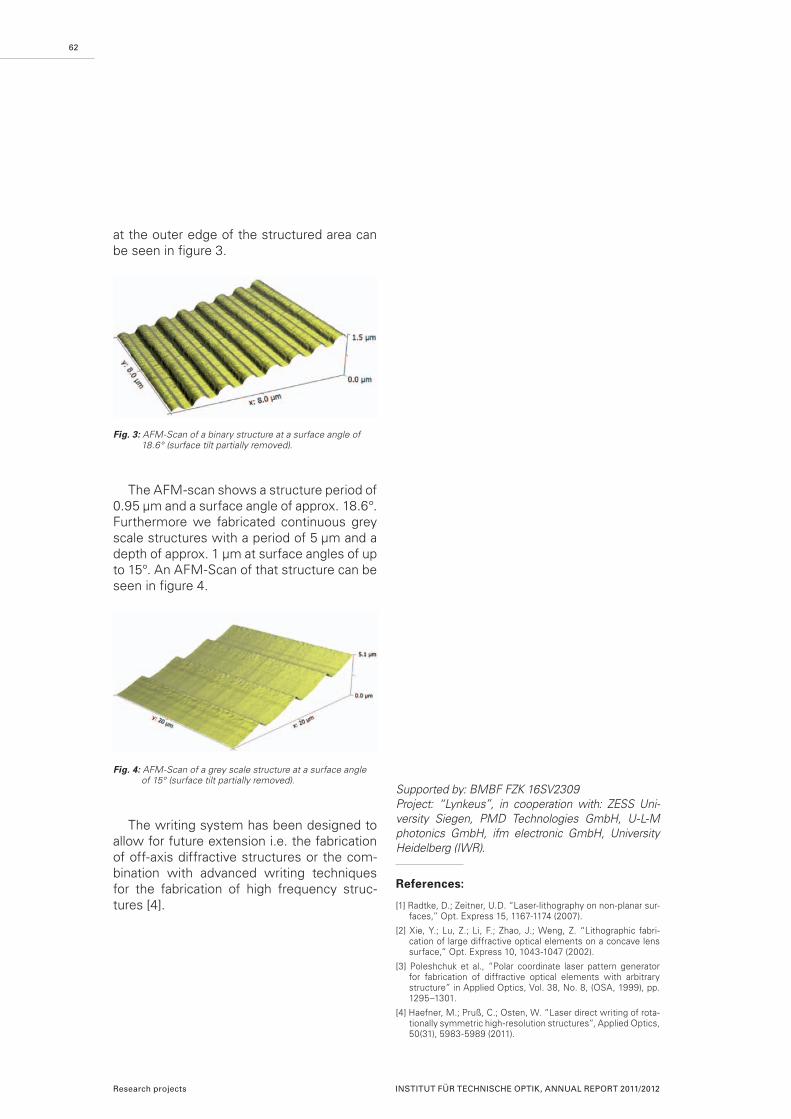
at the outer edge of the structured area can be seen in figure 3.
The AFM-scan shows a structure period of 0.95 µm and a surface angle of approx. 18.6°. Furthermore we fabricated continuous grey scale structures with a period of 5 µm and a depth of approx. 1 µm at surface angles of up to 15°. An AFM-Scan of that structure can be seen in figure 4.
The writing system has been designed to allow for future extension i.e. the fabrication of off-axis diffractive structures or the com-bination with advanced writing techniques for the fabrication of high frequency struc-tures [4].
62
Research projects INSTITUT FÜR TECHNISCHE OPTIK, ANNUAL REPORT 2011/2012
Supported by: BMBF FZK 16SV2309Project: “Lynkeus”, in cooperation with: ZESS Uni-versity Siegen, PMD Technologies GmbH, U-L-M photonics GmbH, ifm electronic GmbH, University Heidelberg (IWR).
References:
[1] Radtke, D.; Zeitner, U.D. “Laser-lithography on non-planar sur-faces,” Opt. Express 15, 1167-1174 (2007).
[2] Xie, Y.; Lu, Z.; Li, F.; Zhao, J.; Weng, Z. “Lithographic fabri-cation of large diffractive optical elements on a concave lens surface,” Opt. Express 10, 1043-1047 (2002).
[3] Poleshchuk et al., “Polar coordinate laser pattern generator for fabrication of diffractive optical elements with arbitrary structure” in Applied Optics, Vol. 38, No. 8, (OSA, 1999), pp. 1295–1301.
[4] Haefner, M.; Pruß, C.; Osten, W. “Laser direct writing of rota-tionally symmetric high-resolution structures”, Applied Optics, 50(31), 5983-5989 (2011).
Fig. 3: AFM-Scan of a binary structure at a surface angle of 18.6° (surface tilt partially removed).
Fig. 4: AFM-Scan of a grey scale structure at a surface angle of 15° (surface tilt partially removed).
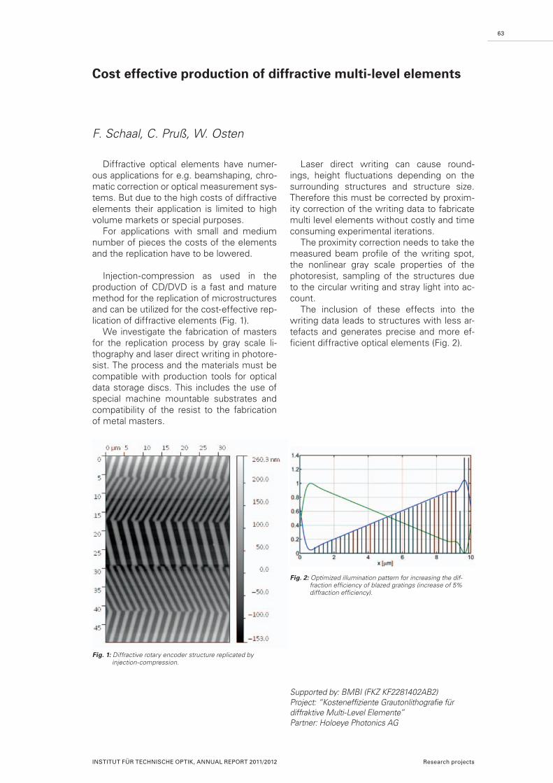
63
Diffractive optical elements have numer-ous applications for e.g. beamshaping, chro-matic correction or optical measurement sys-tems. But due to the high costs of diffractive elements their application is limited to high volume markets or special purposes.
For applications with small and medium number of pieces the costs of the elements and the replication have to be lowered.
Injection-compression as used in the production of CD/DVD is a fast and mature method for the replication of microstructures and can be utilized for the cost-effective rep-lication of diffractive elements (Fig. 1).
We investigate the fabrication of masters for the replication process by gray scale li-thography and laser direct writing in photore-sist. The process and the materials must be compatible with production tools for optical data storage discs. This includes the use of special machine mountable substrates and compatibility of the resist to the fabrication of metal masters.
Cost effective production of diffractive multi-level elements
F. Schaal, C. Pruß, W. Osten
Laser direct writing can cause round-ings, height fluctuations depending on the surrounding structures and structure size. Therefore this must be corrected by proxim-ity correction of the writing data to fabricate multi level elements without costly and time consuming experimental iterations.
The proximity correction needs to take the measured beam profile of the writing spot, the nonlinear gray scale properties of the photoresist, sampling of the structures due to the circular writing and stray light into ac-count.
The inclusion of these effects into the writing data leads to structures with less ar-tefacts and generates precise and more ef-ficient diffractive optical elements (Fig. 2).
Supported by: BMBI (FKZ KF2281402AB2)Project: “Kosteneffiziente Grautonlithografie für diffraktive Multi-Level Elemente” Partner: Holoeye Photonics AG
Fig. 1: Diffractive rotary encoder structure replicated by injection-compression.
Fig. 2: Optimized illumination pattern for increasing the dif-fraction efficiency of blazed gratings (increase of 5% diffraction efficiency).
INSTITUT FÜR TECHNISCHE OPTIK, ANNUAL REPORT 2011/2012 Research projects

One of the major issues that prevented the wide use of diffractive elements in op-tical systems is still the availability of these high precision optical elements. At the insti-tute we maintain a long tradition of design and fabrication of diffractive optical elements – our first writing system was installed in the 70s. In 1995 we started to produce high pre-cision diffractive optical elements (DOE) in a laser direct writing process and have continu-ously developed our laser writing capabilities since then, including gray scale lithography, scanning interference lithography, writing on curved substrates.
Our fabrication capabilities are available for external partners.
Core of our microstructure fabrication are two circular laser writing systems, flexible high precision tools that work in polar coor-dinates, comparable to a DVD writer. This working principle offers the advantage of a high, continuous scanning speed and fa-cilitated fabrication of rotationally symmetric structures. One of the systems is also ca-pable to write on rotation symmetric curved substrates e.g. lens surfaces.
The writing is not limited to circles but allows writing arbitrary structures such as linear gratings or microlenses. Refractive mi-crostructures and blazed gratings are written in grayscale mode where the writing beam intensity is varied with at the moment up to 256 levels.
The substrate size can vary from a few mil-limeters to 300 mm in diameter. The shape can be rectangular, round or any other rea-
sonable outline. The system allows substrate thicknesses up to 25 mm.
The structures are written directly into photoresist. The resulting photoresist profile is then either used directly (e.g. for master-ing) or is transferred into the fused silica sub-strate using dry etching (ICP).
Example applications that we have de-signed and developed with academic and in-dustrial partners are:
CGH for aspheric testing Custom made diffractive and refractive mi-
crolens arrays Beam shaping elements DOE for optical sensors DOE for imaging systems Custom phase structures Phase contrast plates Nipkow microlens disks Master fabrication for mass replication Writing on curved substrates e.g. for chro-
matic correction of optical systems
64
Fabrication of diffractive and micro-optical elements for external partners
F. Schaal, C. Pruß, W. Osten
Fig. 1: Aspheric refractive micro lens array.
Fig. 2: Double sided diffractive micro lens array with individu-ally optimized lenses.
Fig. 3: DOE on a lens surface.
Research projects INSTITUT FÜR TECHNISCHE OPTIK, ANNUAL REPORT 2011/2012

The German part of the trilateral DFG-proj-ect “Inverse source and inverse diffraction problems in photonics” deals with the detec-tion of phase errors in CGH’s introduced by rigorous effects.
A common test for aspheres and freeform surfaces is the null test. Here a CGH is intro-duced in the object path of an interferometer to generate a phase front that matches the surface under test. As the line densities of the CGH are becoming higher, it is no longer sufficient to use scalar approximation [1, 2]. This changes also the influence of fabrication errors onto the reconstructed phase [3].
For a comparison the reconstructed phase of a binary grating in reflection was calcu-lated with scalar approximation and rigorous simulation. The period of the grating was de-creased from 6 to 1 µm, see figure. For grat-ing periods smaller than 2.8 µm or 4.5 the phase difference is larger than /100.
The influence of fabrication tolerances was studied for different gratings (binary, multi level, blazed) with periods of 1µm. Therefore the phase difference between the desired grating and a grating with a variation of 1 % in one parameter was analysed. To determine which effects can still be described by scalar approximation the scalar phase difference for the same parameter variation was subtracted.
The studied grating parameters were duty
cycle, height and side wall angle. In addition
the influence of polarisation and angle of inci-dence were evaluated and showed a signifi-cant phase change, see figure.
Future work will focus on solving the in-verse problem between generated phase and measurable quantities.
65
Phase errors introduced in CGH by rigorous effects
S. Peterhänsel, C. Pruß, W. Osten
Fig. 1: Comparison of scalar approximation and rigorous simu-lation for a binary grating with DC of 0.5 and variable grating period.
Fig. 2: Phase errors for binary gratings with variations of 1%, 1. order, TM polarised light and incidence angles of ± 0.5 NA.
Supported by: DFG (OS111/32-1)Project: “Inverse source and inverse diffraction problems in photonics ”Partners: University of Joensuu, Finland and Tsinghua University, China
References:
[1] Kley, E.-B.; Rockstroh, W.; Schmidt, H.; Drauschke, A.; Wyrowski, F.; Wittig, L.-C. “Investigation of large null-CGH realization”, Proc. SPIE 4440 (2001).
[2] Iff, W.; Glaubrecht, S.; Lindlein, N.; Schwider, J. “Untersuc-hung der Abweichungen zwischen skalarer und rigoroser Rechnung an CGHs in Twyman-Green-Interferometern zur Linsenprüfung”, DGaO Proceedings (2010).
[3] Zhou, P.; Burge, J.H. “Fabrication error analysis and experi-mental demonstration for computergenerated holograms”, Appl. Opt. 46 657–663 (2007).
INSTITUT FÜR TECHNISCHE OPTIK, ANNUAL REPORT 2011/2012 Research projects
Δφ = Δφrigorous – Δφscalar

66
Research projects INSTITUT FÜR TECHNISCHE OPTIK, ANNUAL REPORT 2011/2012

67
Optical methods for assessment of transport and age induced damages on artworks ............................................................................... 68 Supported by: DFG (OS 111/34-1)Project: „Die materielle Veränderung von Kunst durch Transporte“
High resolution 3D microscopy using opposed-view dark-field digital holography ........................................................................................... 69 Supported by: DFG (OS 111/32-1)Project: “High resolution 3D microscopy using opposed-view dark-field digital holography”
3D UV holographic microscope for biomedical imaging .............................................. 72 Supported by: DFG (OS111/19-3)Project: “Digitale Holographie mit adaptiver Wellenfrontformung zur hochauflösenden Untersuchung von 3D-Mikrostrukturen im tiefen UV-Bereich”
Knowledge management in virtual labs and remote experiments ................................ 73 Supported by: Ministerium für Wissenschaft, Forschung und Kunst Baden-Wuerttemberg (MWK)Project: „BW-eLAB“
Compression of digital holograms ................................................................................. 75
Nanometric in-plane displacement measurement using phase singularities ............... 76 Supported by: DAAD
Short temporal coherence digital holography with a femtosecond frequency comb laser for optical sectioning .......................................... 77
Holographic recording of incoherently illuminated or self-luminous objects ............... 78 Supported by: Alexander von Humboldt foundation
Phase retrieval with resolution enhancement by using random-phase illumination ...... 79 Supported by: Alexander von Humboldt foundation
Structured illumination for resolution enhancement and autofocusing in digital holographic microscopy ..................................................... 80 Supported by: Alexander von Humboldt foundation
Coherent Metrology
INSTITUT FÜR TECHNISCHE OPTIK, ANNUAL REPORT 2011/2012 Research projects

Cultural heritage plays a significant role in the development of a society. Therefore, it is of great interest to make works of art acces-sible to the general public. The subsequent increase of museum loan services increases the risk of accelerated degeneration. Hence, in addition to the age related deterioration, transportation can be another source of dam-age. Despite modern packaging technologies, smallest vibrations and environmental climate change can add up and damage the trans-ported object. In order to preserve and restore our cultural heritage it is necessary to detect damages at an early stage before they reach a critical extend. Optical structural diagnosis techniques like shearography can provide the necessary means to identify those defects [1].
Shearography is a coherent-optical measur-ing technique sensitive to the gradient of de-formation. In order to detect structural defects the object is illuminated by an expanded laser beam (see Fig. 1). The optically rough surface scatters the incident light forming a speckle pattern, which is imaged through a Michelson interferometer by a CCD camera. One mirror of the interferometer is slightly tilted produc-ing a pair of laterally sheared images. An infra-red lamp is used to thermally load the object under investigation. Sheared speckle interfer-ograms before and after thermal loading are processed to obtain shearograms. The fringe pattern of a shearogram describes a relative difference in the phase, which is related to the derivative of deformation and therefore to in-ner stress caused by structural defects.
Recently the Stuppach Madonna (painted 1514 – 1516), a painting by Matthias Grüne–wald, was investigated with shearography (see Fig. 2) after the return from the exhibi-tion “Himmlischer Glanz. Raffael, Dürer und Grünewald malen die Madonna” in Dresden, Germany. In addition to the necessary process of restoration the condition of the panel paint-ing should be evaluated and recorded where shearography was applied to assist the con-servators. Due to the size (186 cm × 150 cm) the painting was segmented into 16 subareas. For each subarea a separate shearographic measurement was conducted. The shearo-grams revealed a variety of defects like bub-bles, delaminations and tunnels caused by
wood worms. Even the planking of the wood-en panel and putty could be observed. [2]
Supported by: DFG (OS 111/34-1)Project: „Die materielle Veränderung von Kunst durch Transporte“ In cooperation with: Staatliche Akademie der Bilden-den Künste Stuttgart
References:
[1] Groves, R.; et al. “Shearography as part of a multi-functional sensor for the detection of signature features in moveable cul-tural heritage”, Proc. SPIE 6618, 2007.
[2] Osten, W.; Wilke, M.; Pedrini; G. “Remote Laboratories for Optical Metrology: From the Lab to the Cloud”, Proc. SPIE 8413, 2012.
68
Optical methods for assessment of transport and age induced damages on artworks
M. Morawitz, I. Alexeenko, M. Wilke, G.Pedrini, W.Osten
Fig. 2: Stuppach Madonna before restoration. The shearo-grams show different kinds of defects like bubbles, delaminations (red) and tunnels caused by wood worms (blue). Some features of the painting like the planking (yellow) and putty (green) are also observable.
Fig. 1: Shearography setup. The object under test is illumi-nated by an expanded laser beam. The resulting speckle pattern is imaged through a Michelson interferometer with a CCD camera before and after thermal loading the object with an infrared lamp.
Research projects INSTITUT FÜR TECHNISCHE OPTIK, ANNUAL REPORT 2011/2012

69
The aim of this DFG project is to develop a label-free three-dimensional microscopy sys-tem to enhance the spatio-temporal resolu-tion and the contrast in imaging of complex biological samples. The lateral resolving pow-er of an optical system is diffraction-limited according to Abbe Criterion. Considering the fact that complex specimens consist of dif-ferent materials in various layers, there are some practical obstacles that prevent achiev-ing the theoretical resolution, e.g. the diffrac-tion patterns coming from the upper layers. Here, we are developing a coherent micros-copy method to overcome this limitation us-ing an opposed-view approach.
In the setup, four off-axis digital holograph-ic microscopes (DHM) have been combined in one configuration to record digital holo-grams in two illumination modes (dark-field and bright-field), from two opposing views of the sample. Two different wavelengths were used to be able to separate the dark-field and bright-field signals for each imag-ing view. The wavelength selection depends on the absorption/transmission coefficient and scattering property of materials inside the sample. To perform dark-field imaging, we used a wavelength in the low frequency spectrum of the visible window, in which bio-logical samples have higher scattering rate. A single mode laser diode, operating at 660 nm, was used as a light source for this imag-ing mode. For the bright-field imaging mode, the wavelength of 405 nm was utilized. This wavelength is in the high frequency region of the visible spectrum that provides with a higher resolution and also a higher contrast due to the relatively higher absorption coef-ficient of the biological tissue.
Figure 1 shows the schematic diagram and a photo of the actual setup in the laboratory. A pair of Nikon dark/bright-field objectives, with the magnification of 20x and NA=0.45, has been implemented in the setup. Each objective creates a hollow light cone to pro-duce dark-field illumination and is designed in a way to be capable of simultaneously imag-ing with dark-field and bright-field illumination in both transmission and reflection modes. Two CCD cameras have been installed in each view; one to collect the dark-field and
High resolution 3D microscopy using opposed-view dark-field digital holography
A. Faridian, G. Pedrini, W. Osten
the other to collect the bright-field signal. The entire dark-field signal is directed to the cor-responding CCDs using the dichroic mirrors installed in the imaging path (DM1 and DM2). The bright-field signal is transmitted through the dichroic mirrors and guided to the corre-sponding CCDs by the beam-splitters BS1 and BS2.
We took the larvae of sea urchin (about 24 hours old) for our investigations. Figure 2 shows the digitally reconstructed images of a larva taken by the top view (left column) and also the bottom view (right column) DHM.
Fig. 1: Top: Schematic diagram of the imaging part of the opposed-view DHM setup, showing both dark-field and bright-field configuration. Bottom: the arranged actual setup in the laboratory.
INSTITUT FÜR TECHNISCHE OPTIK, ANNUAL REPORT 2011/2012 Research projects

In this example, the larva was kept floating in a water. The reconstructed images which are shown in Fig. a1) and b1) correspond to a specific larva taken from the top and bot-tom view, respectively. Figures c1) and d1) show the corresponding phase for each view. Figures a2) and b2) represents the re-constructed images of another neighbouring larva in the same medium and c2), d2) rep-resents the corresponding phase. Comparing (a) and (b), one can see the difference in the structures from different imaging views for a given focused image plane.
For this sample, a clean water environ-ment containing only a few larvae has been prepared; otherwise the presence of the other particles in the upper (or lower) layers could reduce the image quality from a given imaging view by creating some diffraction patterns. However, the opposed view sys-tem is also intended to improve the image quality it in this case.
To present the dark-field part of the setup, only the result of the bottom view is reported here. To be able to better evaluate the dark-field result, a bright-field image of a larva, taken by a 405 nm laser diode, is presented in figure 3.a). A dark-field image of the lar-va, taken by a 660 nm laser diode, is shown in figure 3.b). Being based on scattering, speckle field noise is inevitable in coherent dark-field microscopy (figure 3.b). Therefore, to supress the speckle noise, we illuminated the sample with various speckle fields and derived the final image by averaging over the fields. Figures c-d) represents two differ-ent focuses of dark-field image of the larva after averaging over 100 speckle field illumi-nations. Figures 3b) and 3d) are in the same focusing position.
70
Research projects INSTITUT FÜR TECHNISCHE OPTIK, ANNUAL REPORT 2011/2012
Fig. 2: Left column: reconstructed intensity (a1, a2) and phase (c1, c2) images of two sea urchin larvae, floating in a water medium, taken from the top view. Right column: reconstructed intensity (b1, b2) and phase (d1, d2) images of two sea urchin larvae, floating in a water medium, taken from the bottom view.
Fig. 3: a) Bright-field image of a larva taken using a 405 nm laser diode, b) dark-field image of the larva illuminated by a speckle field of a 660 nm laser diode, c-d) two different focuses of dark-field image of the same larva after averaging over 100 speckle field illuminations.
Fig. 4: Reconstructed intensity image of two larvae averaged over 100 speckle fields, figures (a-d) shows sequential digital focusing for different layers of the larvae.
71
Therefore, the holograms are also record-ed using different speckle field illuminations. Figure 4 represents different focuses of the reconstructed intensity images of two larvae, averaged over 100 holograms, which were recorded sequentially using a Labview pro-gram in about 10 seconds; the process can be even much faster utilizing a high speed Camera.
Compared to the bright-field image, the skeleton of the larvae is visible with more contrast and the sharp focus plane is easier to find for a specific region of interest. Also, some internal structures of the body, which have more scattering rate, are more recogniz-able in the dark-field images.
INSTITUT FÜR TECHNISCHE OPTIK, ANNUAL REPORT 2011/2012 Research projects
Supported by: DFG (OS 111/32-1)Project: “High resolution 3D microscopy using op-posed-view dark-field digital holography”
References:
[1] Faridian, A.; G. Pedrini, G.; Osten, W. “High contrast multi-layer imaging of biological organisms through dark-field digital refocusing”, submitted to the Journal of Biomedical Imaging, SPIE Journals.

Digital holographic microscopy (DHM) is a combination of holography and microscopy and has the ability to extract essential 3D in-formation from a single recording. With the help of numerical reconstruction and digital focusing DHM has become a new tool for biomedical imaging.
Like in conventional microscopy, in DHM the diffraction-limited lateral resolution, intro-duced by the Abbe’s criterion (λ / NA), can be increased either by increasing the NA of the optical system or by using shorter wave-lengths.
The main purpose of our investigations is to increase the resolution and the contrast for the imaging of live cells. For this purpose we built an off-axis DHM set-up using high NA objective (0.75) and UV light sources in the range of 193 nm to 355 nm. To avoid stray reflections and aberrations least possible op-tical components are used.
In the beginning we used a laser source having wavelength 193 nm and we could achieve a lateral resolution of 250 nm how-ever this kind of light is almost fully absorbed by living cells and thus essential informations are lost. Figure 1 shows the reconstructed amplitude (a) and the phase (b) of HeLa cells which were recorded with the 193 nm wave-length light source. The current investiga-tions are focused on longer wavelengths. We used 355 nm for imaging but the absorbance of live cells at this wavelength is 10-15 % and thus the cells are nearly transparent and the contrast of the images is very poor. Figure 2 shows the images of reconstructed ampli-tude (a) and the calculated phase (b).
Currently we are using 266 nm light source. The absorbance at this wavelength is more than 50 % and live cells are semi-transparent to this wavelength, creating an ideal condition for high contrast imaging. Fig-ure 3 shows the high contrast and resolution images of live cells at 266 nm. Figure 3 (a), (b) and (c) show the reconstructed amplitude, the calculated phase map and 3D image of the HeLa cell.
Supported by: DFG (OS111/19-3)Project: “Digitale Holographie mit adaptiver Wellen-frontformung zur hochauflösenden Untersuchung von 3D-Mikrostrukturen im tiefen UV-Bereich”
References:
[1] Faridian, A.; Hopp, D.; Pedrini, G.; Eigenthaler, U.; Hirscher, M.; Osten, W. “Nanoscale imaging using deep ultraviolet digital holographic microscopy”, Opt. Exp, 18, 14159:14164, 2010.
72
3D UV holographic microscope for biomedical imaging
A. K. Singh, A. Faridian, G. Pedrini, W. Osten
Fig. 1: Imaging of Hela cell using 193 nm wavelength light source (a) reconstructed amplitude and (b) Phase map.
Fig. 2: HeLa cell imaging using 355 nm wavelength light source (a) reconstructed amplitude (b) calculated phase map.
Fig. 3: (a) reconstructed amplitude (b) phase map and (c) 3D image of HeLa cell with 266 nm wavelength light source.
Research projects INSTITUT FÜR TECHNISCHE OPTIK, ANNUAL REPORT 2011/2012
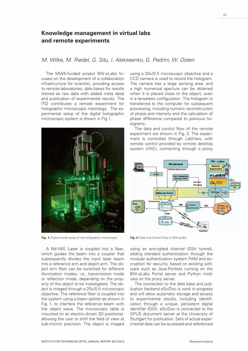
73
The MWK-funded project BW-eLabs fo-cuses on the development of a collaboration infrastructure for scientist, providing access to remote laboratories, data bases for results (stored as raw data with added meta data) and publication of experimental results. The ITO contributes a remote experiment for holographic microscopic metrology. The ex-perimental setup of the digital holographic microscopic system is shown in Fig 1.
A Nd-YAG Laser is coupled into a fiber, which guides the beam into a coupler that subsequently divides the input laser beam into a reference arm and object arm. The ob-ject arm fiber can be switched for different illumination modes, i.e., transmission mode or reflection mode, depending on the prop-erty of the object to be investigated. The ob-ject is imaged through a 20x/0.5 microscopic objective. The reference fiber is coupled into the system using a beam splitter as shown in Fig. 1, to interfere the reference beam with the object wave. The microscopic table is mounted on an electric-driven 3D positioner, allowing the user to shift the field of view at sub-micron precision. The object is imaged
Knowledge management in virtual labs and remote experiments
M. Wilke, M. Riedel, G. Situ, I. Alekseenko, G. Pedrini, W. Osten
using a 20x/0.5 microscopic objective and a CCD camera is used to record the hologram. The camera has a large sensing area, and a high numerical aperture can be obtained when it is placed close to the object, even in a lenseless configuration. The hologram is transferred to the computer for subsequent processing, including numeric reconstruction of phase and intensity and the calculation of phase difference compared to previous ho-lograms.
The data and control flow of the remote experiment are shown in Fig. 2. The experi-ment is controlled through LabView, with remote control provided by remote desktop system (VNC), connecting through a proxy
using an encrypted channel (SSH tunnel), adding standard authentication through the modular authentication system PAM and en-cryption for security, based on existing soft-ware such as Java-Portlets running on the BW-eLabs Portal server and Python mod-ules on the proxy server.
The connection to the data base and pub-lication backend eSciDoc is work in progress and will allow automatic storage and access to experimental results, including identifi-cation through a unique, persistent digital identifier (DOI). eSciDoc is connected to the OPUS document server at the University of Stuttgart for publication. Sets of actual exper-imental data can be accessed and referenced
Fig. 1: Experimental setup of the holographic microscope. Fig. 2: Data and Control Flow in BW-eLabs
INSTITUT FÜR TECHNISCHE OPTIK, ANNUAL REPORT 2011/2012 Research projects

through OPUS, using the DOI identifiers. In addition to the generic access using
VNC, a 3D virtual environment (Wonder-land) is being implemented. This frontend is intended to provide intuitive access to the hardware, as well as support collaboration between users by providing communication channels.
74
Research projects INSTITUT FÜR TECHNISCHE OPTIK, ANNUAL REPORT 2011/2012
Supported by: Ministerium für Wissenschaft, Forschung und Kunst Baden-Wuerttemberg (MWK)Project: „BW-eLAB“ Partners: RUS, UB (University of Stuttgart); FMF, Re-chenzentrum (University of Freiburg); FIZ Karlsruhe; Stuttgart Media University
References:
[1] Wilke, M. ; Alekseenko, I. ; Situ, G. ; Sarker, K.; Riedel, M. ; Pe-drini, G.; Osten, W. „Remote laboratory for digital holographic metrology“, Proc. SPIE 8082, Optical Measurement Systems for Industrial Inspection VII, 80820D (May 26, 2011).
Fig. 3: User Interface
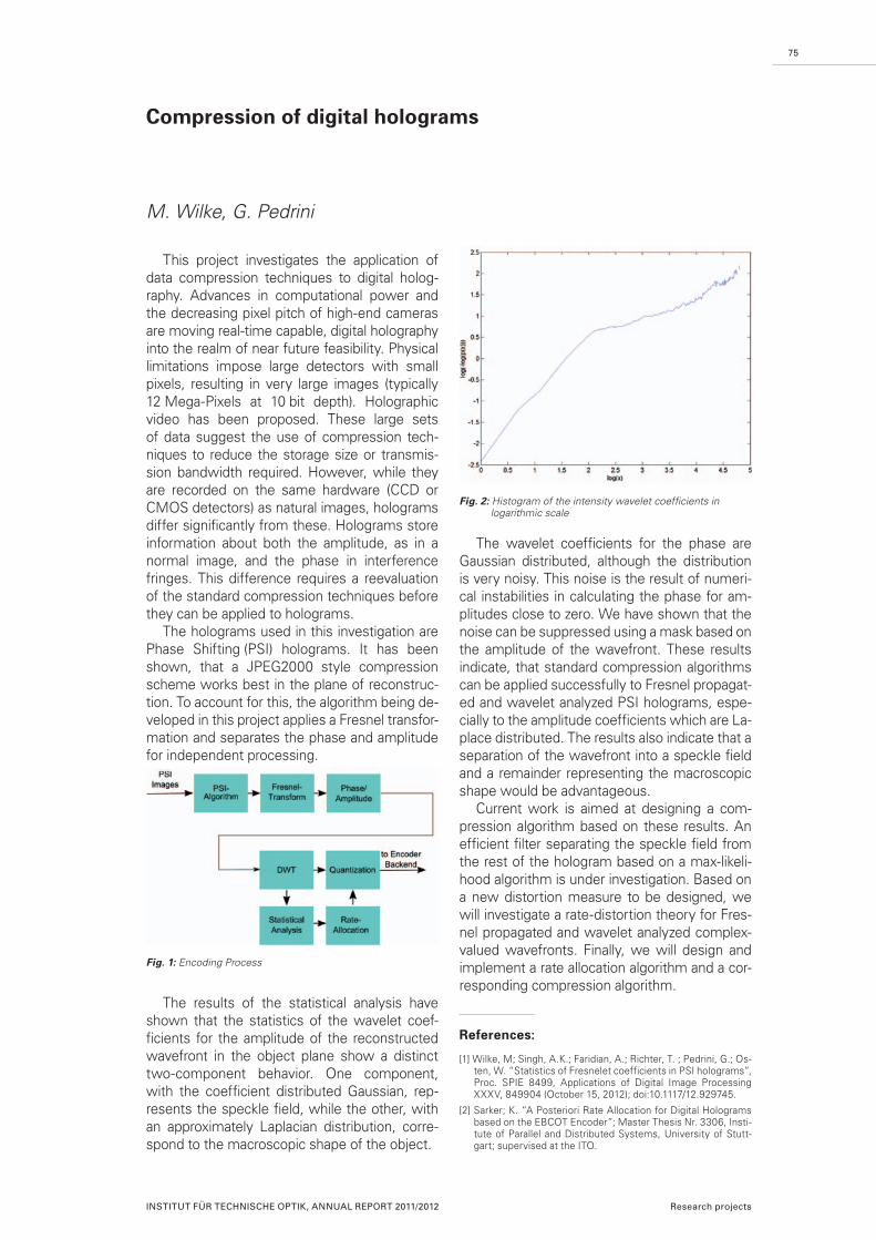
This project investigates the application of data compression techniques to digital holog-raphy. Advances in computational power and the decreasing pixel pitch of high-end cameras are moving real-time capable, digital holography into the realm of near future feasibility. Physical limitations impose large detectors with small pixels, resulting in very large images (typically 12 Mega-Pixels at 10 bit depth). Holographic video has been proposed. These large sets of data suggest the use of compression tech-niques to reduce the storage size or transmis-sion bandwidth required. However, while they are recorded on the same hardware (CCD or CMOS detectors) as natural images, holograms differ significantly from these. Holograms store information about both the amplitude, as in a normal image, and the phase in interference fringes. This difference requires a reevaluation of the standard compression techniques before they can be applied to holograms.
The holograms used in this investigation are Phase Shifting (PSI) holograms. It has been shown, that a JPEG2000 style compression scheme works best in the plane of reconstruc-tion. To account for this, the algorithm being de-veloped in this project applies a Fresnel transfor-mation and separates the phase and amplitude for independent processing.
The results of the statistical analysis have shown that the statistics of the wavelet coef-ficients for the amplitude of the reconstructed wavefront in the object plane show a distinct two-component behavior. One component, with the coefficient distributed Gaussian, rep-resents the speckle field, while the other, with an approximately Laplacian distribution, corre-spond to the macroscopic shape of the object.
The wavelet coefficients for the phase are Gaussian distributed, although the distribution is very noisy. This noise is the result of numeri-cal instabilities in calculating the phase for am-plitudes close to zero. We have shown that the noise can be suppressed using a mask based on the amplitude of the wavefront. These results indicate, that standard compression algorithms can be applied successfully to Fresnel propagat-ed and wavelet analyzed PSI holograms, espe-cially to the amplitude coefficients which are La-place distributed. The results also indicate that a separation of the wavefront into a speckle field and a remainder representing the macroscopic shape would be advantageous.
Current work is aimed at designing a com-pression algorithm based on these results. An efficient filter separating the speckle field from the rest of the hologram based on a max-likeli-hood algorithm is under investigation. Based on a new distortion measure to be designed, we will investigate a rate-distortion theory for Fres-nel propagated and wavelet analyzed complex-valued wavefronts. Finally, we will design and implement a rate allocation algorithm and a cor-responding compression algorithm.
References:
[1] Wilke, M; Singh, A.K.; Faridian, A.; Richter, T. ; Pedrini, G.; Os-ten, W. “Statistics of Fresnelet coefficients in PSI holograms”, Proc. SPIE 8499, Applications of Digital Image Processing XXXV, 849904 (October 15, 2012); doi:10.1117/12.929745.
[2] Sarker; K. “A Posteriori Rate Allocation for Digital Holograms based on the EBCOT Encoder”; Master Thesis Nr. 3306, Insti-tute of Parallel and Distributed Systems, University of Stutt-gart; supervised at the ITO.
75
Compression of digital holograms
M. Wilke, G. Pedrini
INSTITUT FÜR TECHNISCHE OPTIK, ANNUAL REPORT 2011/2012 Research projects
Fig. 1: Encoding Process
Fig. 2: Histogram of the intensity wavelet coefficients in logarithmic scale

The measurement of deformations is of great importance for confirming analytical and finite element models, accessing mate-rial and device properties, detecting potential defects and determining performance. For some applications, it is necessary to mea-sure deformation with accuracies down to the lower nanometer range.
Phase singularities are present in wave fields reflected or transmitted by an object and are very sensitive to any kind of distur-bance, thus by tracking them we may mea-sure small in-plane displacements.
The phase singularities are the zeros of the wave field. Let an analytical signal ψ be writ-ten in terms of its real and imaginary parts, ξ, η as
the occurrence of singularity requires ψ = O; and for that the real and imaginary part of the amplitude ξ, η must be zero. If we draw zero contours of real and imaginary parts of com-plex amplitude this condition is only satisfied at the intersection of the two contours. As shown in Fig. 1 (green and red lines are the contours of zeros for real and imaginary parts of the complex amplitude respectively) the contours intersect each other at the phase singularities (encircled).
The position of the singularities was deter-mined by using bilinear interpolation allowing the identification of their location with an ac-curacy of 0.001 pixels. The displacement of any object surface may be obtained by locat-ing the phase singularities before and after the movement.
Experiments were performed to verify the validity of the method. A PZT was used for providing precise displacements and to de-termine the phase, off-axis digital holography method was used. After locating the coordi-nates of all the singularities we measured the given displacements as mentioned above. The histograms of the coordinate changes of the phase singularities were plotted and from their maxima we could calculate the displacement in both the directions. As we increase the applied voltage to the PZT for more displacement we have a displacement of the peak location of the histograms de-
scribing the shift of a set of singularities. Us-ing the shift of the peak we could calculate the nanometric in-plane displacements. Fig-ure 2 shows the displacements (in nm) as a function of the voltage (in mV) applied to the PZT.
76
Nanometric in-plane displacement measurement using phase singularities
A. K. Singh, G. Pedrini, W. Osten
Research projects INSTITUT FÜR TECHNISCHE OPTIK, ANNUAL REPORT 2011/2012
Supported by: DAAD
References:
[1] Kolenovic, E.; Osten, W. “Estimation of the phase error in in-terferometric measurements by evaluation of the speckle field intensity”, App Optics 46, 6096:6104, 2007.
Fig. 1: Speckle pattern reflected from a diffused object and the corresponding zero contours of real and imaginary part of the complex amplitude.
Fig. 2: Relation between the voltage applied to the PZT and the measured displacement.
ψ(r, t) = ξ(r, t) + iη(r, t)

Short coherence digital holography with a femtosecond frequency comb laser source may be applied for multi-level optical sectioning. The object shape is obtained by digital reconstruc-ting and processing a sequence of holograms recorded during stepwise shifting of a mirror in the reference arm of a Michelson interfero- meter [1]–[3].
The used set-up for digital holography with a femtosecond frequency comb laser from Men-loSystems is shown in Fig. 1. The laser speci-fications are as follows: pulse duration 100 fs, λ = 532 nm, Δλ ≈ 10 nm, Δυfc = 5.994 GHz (pulse distance in space Y = 50.00 mm), output power ≈ 50 mW. The laser beam is at first ex-panded and collimated by a telescope and later divided into two parts by a beamsplitter. The reflected and transmitted beams are directed towards the object and a spherical mirror in the reference path, respectively. The wavefronts re-flected by the object and the mirror are recom-bined by the beamsplitter; the CCD camera re-cords the hologram intensity.
The object used for the experimental investi-gations was a rough metallic cone (see Fig. 2a). Figs. 2.b), c), d) show three numerical recon-structions obtained by using a single hologram with digital focusing in three different planes, each separated by 25.00 mm (Y = 50.00 mm).
Fig. 3 presents the 3-d shape of the cone reconstructed from 17 holograms recorded by displacing the reference mirror by 1 mm be-tween each hologram. The axial resolution is given by the step of the scanning and thus more holograms are needed for improving the accu-racy which is limited by the temporal coherence length of one laser pulse that is ≈ 30 µm. The results demonstrate that a set-up based on digi-tal holography using a fs fc-laser can be used for simultaneous multiple optical sectioning.
In the next years, we expect the availability of fc-lasers based on microresonators. In this case, the distance of the sectioning planes can be re-duced to approximately 100 µm and will allow applying the optical sectioning method for tech-nical and biological applications in microscopy. Furthermore, by using powerful frequency comb lasers, the multi level optical sectioning method can also be extended to larger objects which may be located far away from the detecting system (airplanes, building or power plant components).
References:
[1] Körner, K.; Pedrini, G.; Alexeenko, I.; Steinmetz, T.; Holzwarth, R.; Osten, W. “Short temporal coherence digital holography with a femtosecond frequency comb laser for multi-level opti-cal sectioning”, Opt. Express 20, 7237-7242 (2012).
[2] German patent DE 10 2011 016 660 B4 2012.10.25.
[3] Körner, K.; Pedrini, G.; Alexeenko, I.; Lyda, W.; Steinmetz, T.; Holzwarth, R.; Osten, W. “Multi-level optical sectioning based on digital holography with a femtosecond frequency comb la-ser”, Proc. SPIE 8430, 843004 (2012).
77
Short temporal coherence digital holography with a femtosecond frequency comb laser for optical sectioning
K. Körner, G. Pedrini, I. Alexeenko, W. Osten
INSTITUT FÜR TECHNISCHE OPTIK, ANNUAL REPORT 2011/2012 Research projects
Fig. 1: Experimental set-up for lensless short coherence digital holography with a fc-laser at 532 nm with a pulse dis-tance in space Y=50.00 mm referenced to a Rubidium atomic clock.
Fig. 3: Numerical reconstruction of a part of the rough metallic continuous cone.
Fig. 2: a) Schematic of the rough metallic cone used for the in-vestigations, base diameter ≈36 mm, height ≈80 mm, half angle ≈12°. b), c), d) Reconstruction of holograms at three different planes separated by 25.00 mm (Y=50.00 mm).

Traditionally, holography requires coherent-light for illuminating the object and recording its 3-D information. However, various attempts have been made to record a hologram of an incoherently illuminated or self-luminous ob-ject. In such cases, the light emitted by each point could interfere only with itself and a self-referencing scheme is commonly utilized for re-cording of the hologram. We adopt an approach based on statistical optics to describe the pro-cess of recording of an incoherent-object holo-gram as a complex spatial coherence function. The principle behind the proposed scheme is based on van Cittert-Zernike theorem. We dem-onstrate its implementation using a Sagnac ra-dial shearing interferometer for field correlation and a Pockels cell for phase shifting and quanti-fying the coherence function.
Here the object being recorded is a negative transparency of numeral 3 illuminated by an LED Luxeon Star LXHL-MMID, having spectral width at half maximum of about 35nm at wavelength 530 nm. As shown in Fig. 1, the field distribu-tion at the back focal plane of lens L1 is directed into a properly designed common-path Sagnac radial shearing interferometer. A telescopic system with magnification = f3/f2 = 1.067, formed by lenses L2 and L3, introduced inside the interferometer gives a radial shear between the counter propagating beams as they travel through interferometer. The Pockels cell (PC) introduces a phase shift between the orthogo-nally polarized radially sheared beams. One of the interferograms recorded with an 8-bit CCD (Hitachi KP-2FA) is shown in Fig. 2(a). The fringe contrast and the fringe phase that jointly rep-resent the complex spatial coherence function are shown in Figs. 2(b) and 2(c) respectively. For the reconstruction of the object, this complex spatial coherence function is back propagated. The intensities of the reconstructed object at z=–1mm, z=0mm and z=1mm planes are shown in Figs. 3(a-c) respectively. The corre-sponding phase distributions that help to focus different sections of the object through propa-gation are shown in Figs. 3(d-f).
3-D object reconstruction can be achieved even in outdoor environment due to the inher-ent stability provided by the common path inter-ferometer. Due to the implementation of phase shift using a Pockels cell, the system is mechan-
ics free and has a potential for automated fast measurement applicable to dynamic situations.
Supported by: Alexander von Humboldt foundation
References:
[1] Naik, D.N.; Pedrini, G.; Osten, W. “Recording of incoherent-object hologram as complex spatial coherence function using Sagnac radial shearing interferometer and a Pockels cell”, Opt. Express 21, 3990-3995 (2013).
78
Holographic recording of incoherently illuminated or self-luminous objects
D.N. Naik, G. Pedrini, W. Osten
Research projects INSTITUT FÜR TECHNISCHE OPTIK, ANNUAL REPORT 2011/2012
Fig. 1: Experimental set up for recording the hologram as complex spatial coherence function.
Fig. 2: (a) One the interferograms recorded by phase shift us-ing Pockels cell. (b) Fringe contrast and (c) Fringe phase jointly representing the complex spatial coherence func-tion at the back focal plane of Lens L1.
Fig. 3: (a) ,(b) and (c) show the amplitude of the complex spatial coherence function back propagated to z=–1mm, z=0mm and z=1mm respectively.(d),(e) and (f) show the corresponding phase distribution.

79
Phase retrieval with resolution enhance-ment is obtained by using random-phase il-lumination generated by a spatial light modu-lator.
Figure 1(a) shows the setup used for phase retrieval. The light from a laser diode is ex-panded by the telescope system L1–L2, and is then directed to the spatial light modula-tor (SLM). The random patterns on SLM (see Fig. 1(b)) are projected to the sample plane by the relaying system (L3–MO1). The object wave is magnified by the objective MO2 and the lens L4. Then, the diffraction patterns (see Fig. 1(c)) are recorded by a CCD camera, which has a certain distance from the image plane IP of the specimen. Note that the SLM enables to project different random-phase patterns without mechanical movement.
For reconstruction, the complex ampli-tudes of the M random-phase fields are measured in advance and denoted with Ak
il-
lum, and k=1,2,…M. we denote with Ik the dif-fraction patterns of the object wave under Ak
illum. Then, the phase retrieval is performed with the following steps: (1) multiply the am-plitude the kth diffraction pattern with a ran-dom initial phase factor exp(iϕk), (2 propagate Ik exp(iϕk) to the object plane, (3) the calcu-
lated wave is divided by the kth illumination amplitude Ak
illum, and multiplied by the (k+1)th illumination amplitude Ak+1
illum, (4) propagate the newly-obtained object wave to the CCD plane, (5) replace the amplitude of the ob-tained object wave with Ik+1. (6) repeat the iteration loop (2)–(5) by using k+1 instead of k, until the difference between two neigh-bouring reconstruction is smaller than the preset value. Furthermore, the object waves reconstructed from different groups of ran-dom-phase illuminations are averaged in or-der to reduce the noise.
Random-phase illumination can be seen as a superposition of plan waves, which shifts the specimen spectrum in different directions in the Fourier plane. Some of the high frequency components (see the four black dots in Fig. 2(a)), which are beyond the system aperture and cut under on-axis plane wave illumination, can pass through the sys-tem. Thus, the random phase illumination can improve the resolution of the optical sys-
Phase retrieval with resolution enhancement by using random-phase illumination
P. Gao, G. Pedrini, W. Osten
tem, compared with the on-axis plane wave illumination.
To test the resolution enhancement, a transparent structured plate was used as specimen. The images reconstructed by us-ing digital holographic microscopy (DHM) and the phase retrieval method are given in Fig. 2(b) and Fig. 2(c), respectively. Note that DHM is constructed by introducing an additional reference wave. When compare Fig. 2(b) and Fig. 2(c), the resolution improve-ment by the random-phase illumination can be seen, and the quantity of the resolution enhancement depends on the maximum an-gle of the random-phase illumination waves. Furthermore, the random-phase illumination eliminates the stagnation problem in the phase retrieval process.
INSTITUT FÜR TECHNISCHE OPTIK, ANNUAL REPORT 2011/2012 Research projects
Supported by: Alexander von Humboldt foundation
Fig. 1: (a) Experimental setup of phase retrieval. (b) Illumina-tion patterns loaded on SLM; (c) generated diffraction patterns on CCD camera.
Fig. 2: Resolution enhancement of phase retrieval with random-phase illumination; (a) Schematics of resolution enhancement; (b) and (c) reconstructed phase images by the DHM with plane wave illumination and the phase retrieval with random-phase illumination; (d) phase distribution along two lines in (b) and (c).
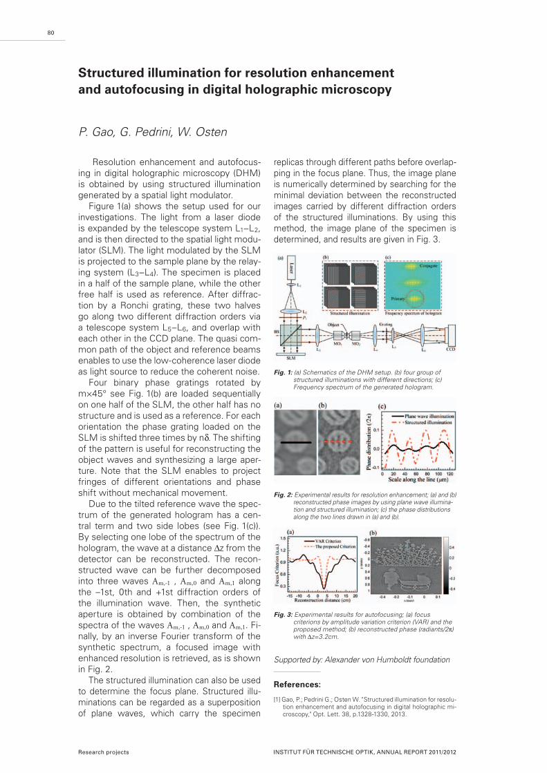
Resolution enhancement and autofocus-ing in digital holographic microscopy (DHM) is obtained by using structured illumination generated by a spatial light modulator.
Figure 1(a) shows the setup used for our investigations. The light from a laser diode is expanded by the telescope system L1–L2, and is then directed to the spatial light modu-lator (SLM). The light modulated by the SLM is projected to the sample plane by the relay-ing system (L3–L4). The specimen is placed in a half of the sample plane, while the other free half is used as reference. After diffrac-tion by a Ronchi grating, these two halves go along two different diffraction orders via a telescope system L5–L6, and overlap with each other in the CCD plane. The quasi com-mon path of the object and reference beams enables to use the low-coherence laser diode as light source to reduce the coherent noise.
Four binary phase gratings rotated by m×45° see Fig. 1(b) are loaded sequentially on one half of the SLM, the other half has no structure and is used as a reference. For each orientation the phase grating loaded on the SLM is shifted three times by nδ. The shifting of the pattern is useful for reconstructing the object waves and synthesizing a large aper-ture. Note that the SLM enables to project fringes of different orientations and phase shift without mechanical movement.
Due to the tilted reference wave the spec-trum of the generated hologram has a cen-tral term and two side lobes (see Fig. 1(c)). By selecting one lobe of the spectrum of the hologram, the wave at a distance Δz from the detector can be reconstructed. The recon-structed wave can be further decomposed into three waves Am,-1 , Am,0 and Am,1 along the –1st, 0th and +1st diffraction orders of the illumination wave. Then, the synthetic aperture is obtained by combination of the spectra of the waves Am,-1 , Am,0 and Am,1. Fi-nally, by an inverse Fourier transform of the synthetic spectrum, a focused image with enhanced resolution is retrieved, as is shown in Fig. 2.
The structured illumination can also be used to determine the focus plane. Structured illu-minations can be regarded as a superposition of plane waves, which carry the specimen
replicas through different paths before overlap-ping in the focus plane. Thus, the image plane is numerically determined by searching for the minimal deviation between the reconstructed images carried by different diffraction orders of the structured illuminations. By using this method, the image plane of the specimen is determined, and results are given in Fig. 3.
Supported by: Alexander von Humboldt foundation
References:
[1] Gao, P.; Pedrini G.; Osten W. "Structured illumination for resolu-tion enhancement and autofocusing in digital holographic mi-croscopy," Opt. Lett. 38, p.1328-1330, 2013.
80
Structured illumination for resolution enhancement and autofocusing in digital holographic microscopy
P. Gao, G. Pedrini, W. Osten
Research projects INSTITUT FÜR TECHNISCHE OPTIK, ANNUAL REPORT 2011/2012
Fig. 1: (a) Schematics of the DHM setup. (b) four group of structured illuminations with different directions; (c) Frequency spectrum of the generated hologram.
Fig. 2: Experimental results for resolution enhancement; (a) and (b) reconstructed phase images by using plane wave illumina-tion and structured illumination; (c) the phase distributions along the two lines drawn in (a) and (b).
Fig. 3: Experimental results for autofocusing; (a) focus criterions by amplitude variation criterion (VAR) and the proposed method; (b) reconstructed phase (radiants/2π) with Δz=3.2cm.

81
INSTITUT FÜR TECHNISCHE OPTIK, ANNUAL REPORT 2011/2012 Research projects
Application of complex surfaces in modern optical design .......................................... 82
Phase space methods in geometrical optics ................................................................. 84
Hybrid endoscopic zoom system with integrated tomographic sensor ...................... 85 Supported by: Baden-Württemberg StiftungProject: “Hyazint”
Optical Design and Simulation
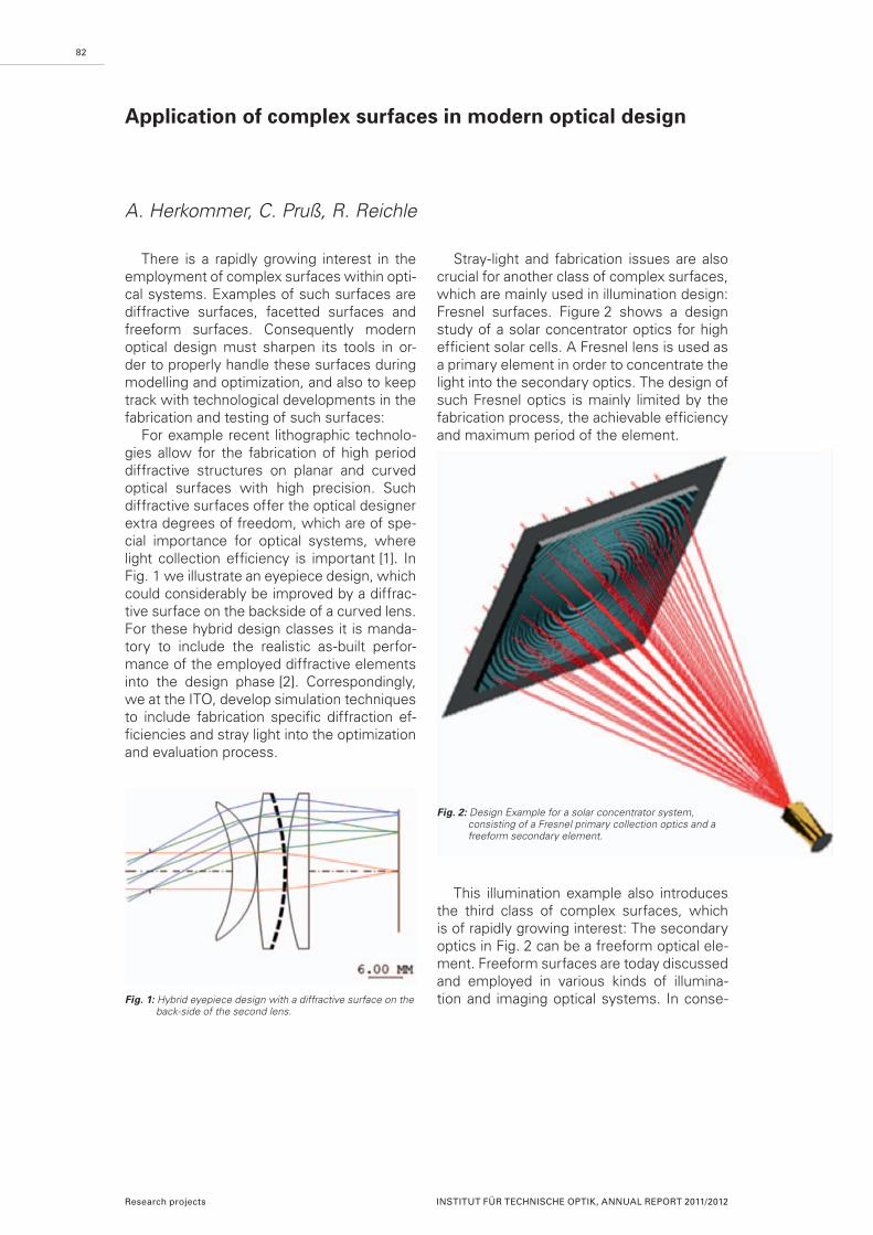
There is a rapidly growing interest in the employment of complex surfaces within opti-cal systems. Examples of such surfaces are diffractive surfaces, facetted surfaces and freeform surfaces. Consequently modern optical design must sharpen its tools in or-der to properly handle these surfaces during modelling and optimization, and also to keep track with technological developments in the fabrication and testing of such surfaces:
For example recent lithographic technolo-gies allow for the fabrication of high period diffractive structures on planar and curved optical surfaces with high precision. Such diffractive surfaces offer the optical designer extra degrees of freedom, which are of spe-cial importance for optical systems, where light collection efficiency is important [1]. In Fig. 1 we illustrate an eyepiece design, which could considerably be improved by a diffrac-tive surface on the backside of a curved lens. For these hybrid design classes it is manda-tory to include the realistic as-built perfor-mance of the employed diffractive elements into the design phase [2]. Correspondingly, we at the ITO, develop simulation techniques to include fabrication specific diffraction ef-ficiencies and stray light into the optimization and evaluation process.
Stray-light and fabrication issues are also crucial for another class of complex surfaces, which are mainly used in illumination design: Fresnel surfaces. Figure 2 shows a design study of a solar concentrator optics for high efficient solar cells. A Fresnel lens is used as a primary element in order to concentrate the light into the secondary optics. The design of such Fresnel optics is mainly limited by the fabrication process, the achievable efficiency and maximum period of the element.
This illumination example also introduces the third class of complex surfaces, which is of rapidly growing interest: The secondary optics in Fig. 2 can be a freeform optical ele-ment. Freeform surfaces are today discussed and employed in various kinds of illumina-tion and imaging optical systems. In conse-
82
Application of complex surfaces in modern optical design
A. Herkommer, C. Pruß, R. Reichle
Research projects INSTITUT FÜR TECHNISCHE OPTIK, ANNUAL REPORT 2011/2012
Fig. 2: Design Example for a solar concentrator system, consisting of a Fresnel primary collection optics and a freeform secondary element.
Fig. 1: Hybrid eyepiece design with a diffractive surface on the back-side of the second lens.

quence methods for the design, the surface description and the fabrication and testing of such components need to be developed, as illustrated in Fig. 3.
At the ITO research is currently performed
and planed in all three areas: During design the main problem is to be in control of the many degrees of freedom during optimiza-tion. A proper surface description is required in order to allow for an efficient optimization and an exact fabrication. Fabrication of free-form surfaces however is only possible is an adequate testing is available.
83
INSTITUT FÜR TECHNISCHE OPTIK, ANNUAL REPORT 2011/2012 Research projects
References:
[1] Herkommer, A.M.; Reichle, R.; Häfner, M.; et al. "Design and simulation of diffractive optical components in fast optical im-aging systems," Proc. SPIE Vol. 8167, 816708 (2011).
[2] Reichle, R.; Pruß, C.; Osten, W. “Diffractive optics in ad-vanced optic design”, ITO annual report 2009/2010.
Fig. 3: Illustration of the interdependence of freeform optical surfaces to the design, surface description and fabrica-tion.

In optical design especially in illumination design, the transport of radiance through the system is important. Typically used compo-nents in illumination design affect the spatial as well as the angular distribution. Therefore it is reasonable to use a description where angle and position can be illustrated simulta-neously. The phase space concept provides an interesting access towards the radiomet-ric quantities. Within an optical system a sin-gle ray is defined by its position and angle in space. Therefore every single ray propagating through the system can be associated with a point in phase space. Thus ray-tracing corre-sponds to a trajectory in phase space [1].
A light source occupies a certain angular and spatial extend witch is a 4 dimensional volume in phase space called etendue. The flux per entendue is the radiance distribution L (x, u) as depicted in Fig. 1. The projection of the radiance to the angular or the spatial axis in phase space allows the calculation of the intensity I (u) and the irradiance E (x).
An analysis of the phase space transforma-tion introduced by optical components pro-vides an entire picture of the optical function-ality. Paraxial free propagation corresponds to a shear of the phase space whereas propa-gation from the front to the back focal plane of a thin lens causes a rotation by 90 degree. Reflection on surfaces leads to a back-folded and mirrored distribution in phase space.
Integrator rods and double arrays are commonly used components in illumination design. Therefore it is of special interest to investigate these elements within the phase space picture [2].
Integrator rods mix the incoming light dis-tribution resulting in a homogenization of the irradiance at the exit of the rod. The incoming light is reflected at the sidewalls of the rod leading to a segmentation of the phase space distribution Fig. 2c).
Optical arrays separate the incoming light in channels due to the apertures of the micro-lens. Different channels are superimposed at the target plane. Fig. 3 shows the phase space distribution at the target plane after a double array and an integrator lens. The ef-fect is similar to the rod a homogenization in position and segmentation in angle.
The analysis of illumination components in phase space offers another access besides classical ray-tracing.
84
Phase space methods in geometrical optics
D. Rausch, A.M. Herkommer
Research projects INSTITUT FÜR TECHNISCHE OPTIK, ANNUAL REPORT 2011/2012
References:
[1] Testorf, M.; Hennelly, B.; Ojeda-Castaneda, J. Phase-space optics. s.l. : McGraw-Hill Companies, 2010.
[2] Rausch, D.; Herkommer, A.M. “Phase space approach to the use of integrator rods and optical arrays in illumination sys-tems”, AOT Vol.1, 2012.
Fig. 2: a) Initial distribution at the entrance of a rectangular integrator rod. b) Distribution after free propagation of the length of the rod. c) Final distribution at the exit of the rod.
Fig. 3: Phase space distribution after propagation through a double array and an integrator lens, leading to a con-stant irradiance E(x) und a discrete intensity I (u).
Fig. 1: Phase space illustration of the radiance L (x, u), intensity I (u) and irradiance E (x).

As a part of the Baden-Württemberg Stif-tung project “Hybride optische Technologien für die Sensorik”, this work aims at the devel-opment of a miniaturized zoom system which combines both, imaging and tomography. In this joint research project our project partner IMTEK (University of Freiburg) is improving and developing microoptical components, while the work at the ITO is focused onto the optical system design.
Extensive research effort has been put on the development of miniaturized active opti-cal elements, such as tunable membrane lenses or micromirrors. The current technol-ogy allows the construction of small integrat-ed active optical systems based on a modu-lar approach (Fig. 1) [1]. As a more complex device, the conceived hybrid sensor system requires a sophisticated and well balanced optical design.
Figure 2 shows the latest concept with a
system diameter of below 2 mm. It comprises two membrane lenses, which can be tuned in-dependently in radius of curvature by applying an external fluid pressure. This enables zoom-ing and focusing without mechanical parts at a high level of integration. Additionally to the imaging beam path which creates an image on the CMOS sensor chip, the system contains a second beam path for optical coherence to-mography (OCT). A MEMS scanning mirror in side-looking configuration enables a laterally resolved OCT signal as well as an extension of field of view for the imaging part. Additional components such as diffractive optical ele-ments (DOE’s) or aspheres can compensate for static aberrations.
In order to narrow down the parameter
space, the concept has been modelled parax-ially as well as within a raytracing software. Realistic lens profiles, obtained by finite ele-ment simulations and tactile measurements have been implemented (Fig. 3). The setup allows a systematic investigation with an automatic optimization in terms of the two lens pressures. Different parameters, such as wavefront errors or vignetting factors can be plotted as a function of working distance and magnification, allowing an evaluation of the expectable optical performance. Due to small numerical apertures given by the sys-tem, diffraction is limiting the achievable im-aging resolution to ~2 µm. This is sufficient to resolve the most relevant features in com-mon endoscopy inspections.
Supported by: Baden-Württemberg StiftungProject: “Hyazint”Cooperation: Gisela-und-Erwin-Sick-Lehrstuhl für Mikrooptik, Institut für Mikrosystemtechnik (IMTEK), Universität Freiburg
References:
[1] Weber, N.; Zappe, H.; Seifert, A. “A tunable optofluidic silicon optical bench", Journal of Microelectromechanical Systems 21 (6), p. 1357-1364, Dec. 2012.
85
Hybrid endoscopic zoom system with integrated tomographic sensor
S. Thiele, A. Herkommer
INSTITUT FÜR TECHNISCHE OPTIK, ANNUAL REPORT 2011/2012 Research projects
Fig. 1: Technology example showing the state of the art. Most of the single components are fabricated by micromach-ing processes (picture delivered by project partner).
Fig. 2: Example for the current concept within the raytracing software ZEMAX.
Fig. 3: a), finite element simulation of a membrane lens with a diameter of 1 mm. b), corresponding surface model (4th order polynomial) implemented in ZEMAX.

PUBLICATIONS 2011 - 2012
Publications 2011 - 2012 INSTITUT FÜR TECHNISCHE OPTIK, ANNUAL REPORT 2011/2012
Invited lectures on international conferences
W. Osten:
From Analog to Digital Holography. What is the Benefit?Sensor and Test Conferences 2011, Nürnberg 2011
W. Osten:
Different approaches to overcome existing limits in optical micro and nano metrology.ICO-22, Puebla, Mexico 2011
W. Osten:
How to overcome physical limitations in optical micro and nano metrology.10th International Conference „Correlation Optics“, Chernivtsy, Ukraine 2011
W. Osten:
What Optical Metrology can do for Experi-mental Mechanics?International Conference on Advances in Experimental Mechanics: Integrating Simulation and Experimentation for Validation (ISEV), 1st joint SEM and BSSM conference, Edinburgh 7-9 September 2011
W. Osten:
Optical micro and nano metrology: limita-tions and solutions.EOS Topical Meeting “Micro- and Nano-Optoelectronic Systems”, Bremen, Dec 7-9, 2011
W. Osten:
Prospects and Challenges for the Optical Inspection of Micro- and Nano-Structures.Micronarc Alpine Meeting MAM 2012, Villars-sur-Ollon, Suisse, Jan 2012
W. Osten:
How to bring your Laboratory in the Cloud? (About the Future of Remote Metrology).Optimess 2012, 5. International Conference on Optical Measurement Techniques, Antwerp, April 4-5, 2012
W. Osten:
Optical Multi-Scale 3D-Metrology or another Kind of Sensor Fusion.International PTB Summer School of Metrology, Burg Warberg, May 2012
W. Osten:
Future Prospects of Remote Metrology.HoloMet 2012, Utsunomiya, Japan, July 2012
W. Osten:
Remote Laboratories for Optical Metrology: From the Lab to the Cloud.Speckle 2012, 5. International Conference on Speckle Metrology, Vigo, Spain, 10-12 Sept. 2012
W. Osten:
Inverse Problems in Optical Metrology: Exemplary Solving Strategies.Chinese-German Binational Workshop on Inverse Problems, Sarbrücken, 8. – 12. Oct. 2012
W. Osten:
Model-based reconstruction of periodic sub-λ features.Leibniz-Konferenz "Sensorsysteme 2012", Lichtenwalde, 18.10. - 19.10.2012
M. Gronle:
Concepts for an active inspection of three-dimensional objects using a multi-sensor measurement system.OaM 2012, Optics and Measurement 2012, Liberec, Czech Republic, 16. - 18. Oct., 2012
W. Osten:
A Remote Laboratory for Optical Metrology: Prospects for the Embedding of Experimental Facilities in a Cloud Computing Environment.2012 IUTAM Symposium on Advances of Optical Methods in Experimental Mechanics, Taipeh, 3. – 6. Nov. 2012

INSTITUT FÜR TECHNISCHE OPTIK, ANNUAL REPORT 2011/2012 Publications 2011 - 2012
87
W. Osten:
The Future of Optical Metrology: Challenges and Prospects.7th ISEM´12, Taipeh 8. – 11. Nov. 2012
T. Haist:
SLM-based multipoint vibrometry.OSA Topical Meeting “Sensor” 2012, 24-28 June 2012, Monterey, USA
Awards: 2011 – 2012
W. Osten
Dennis Gabor Award 2011, SPIE
H. Tiziani
Chandra S. Vikram Award 2012, SPIE
Editorial work
Lehmann, P., Osten, W.; Gastinger, K. (Eds.):
Optical Measurement Systems for Industrial Inspection VII.Proc. SPIE Vol. 8082, Bellingham 2011
Gorecki, C.; Asundi, A.; Osten, W. (Eds.):
Optical Micro- and Nanometrology in Microsystems Technology.Proc. SPIE Vol. 8430, Bellingham 2012

Publications 2011 - 2012 INSTITUT FÜR TECHNISCHE OPTIK, ANNUAL REPORT 2011/2012
Reviewed papers, books and book chapters
Ahmed, M. Abdou; Haefner, M.; Vogel, M.; Pruß, C.; Voss, A.; Osten, W.; Graf, T.
High-power radially polarized Yb: YAG thin-disk laser with high efficiencyOptics Express 19 (2011) 6 pp. 5093
Almoro, P. F.; Pedrini, G.; Gundu, P. N.; Osten, W.; Hanson, S. G.
Enhanced wavefront reconstruction by ran-dom phase modulation with a phase diffuserOptics and Lasers in Engineering 49 (2011) 2 pp. 252–257
Almoro, P.; Pedrini, G.; Osten, W.; Narayanamurthy, C.
Analysis of Bessel beam propagation in free space using digital holographic microscopyOptik - International Journal for Light and Electron Optics (online available 2012)
Almoro, P. F.; Waller, L.; Agour, M.; Falldorf, C.; Pedrini, G.; Osten, W.; Hanson, S. G.
Enhanced deterministic phase retrieval using a partially developed speckle fieldOptics Letters 37 (2012) 11 pp. 2088
Anand, A.; Faridian, A.; Chhaniwal, V.; Pedrini, G.; Osten, W.; Javidi, B.
High-resolution quantitative phase micro-scopic imaging in deep UV with phase retrievalOptics Letters 36 (2011) 22 pp. 4362
Bao, P.; Pedrini, G.; Osten, W.
Optical surface profile measurement using phase retrieval by tuning the illumination wavelengthOptics Communications 285 (2012) 24 pp. 5029–5036
Bao, P.; Situ, G.; Pedrini, G.; Osten, W.
Lensless phase microscopy using phase retrieval with multiple illumination wave-lengthsApplied Optics 51 (2012) 22 pp. 5486
Berger, R.; Fleischle, D.; Körner, K.; Lyda, W.; Osten, W.; Sobotka, A.; Wenzel, C.; Brecher, C.
Interferometrische Messung von Freiform-Schneidkanten auf einer Diamantwerkzeug-bearbeitungsmaschinetm - Technisches Messen 78 (2011) 10 pp. 439–446
Bilski, B.; Frenner, K.; Osten, W.
About the influence of Line Edge Rough-ness on measured effective–CDOptics Express 19 (2011) 21 pp. 19967
Burla, A.; Haist, T.; Lyda, W.; Osten, W.
Fourier descriptors for defect indication in a multiscale and multisensor measurement systemOptical Engineering 50 (2011) 4 pp. 43603
Burla, A.; Haist, T.; Lyda, W.; Osten, W.
Genetic programming applied to automatic algorithm design in multi-scale inspection systemsOptical Engineering 51 (2012) 6 pp. 67001
Dolev, S.; Haist, T.; Oltean, M.
Optical supercomputing: introduction to special issueThe Journal of Supercomputing 62 (2012) 2 pp. 617–619
Dong, S.; Haist, T.; Osten, W.
Hybrid wavefront sensor for the fast detec-tion of wavefront disturbancesApplied Optics 51 (2012) 25 pp. 6268
Dong, S.; Haist, T.; Osten, W.; Ruppel, T.; Sawodny, O.
Response analysis of holography-based modal wavefront sensorApplied Optics 51 (2012) 9 pp. 1318
88

INSTITUT FÜR TECHNISCHE OPTIK, ANNUAL REPORT 2011/2012 Publications 2011 - 2012
89
Ferreras Paz, V.; Peterhänsel, S.; Frenner, K.; Osten, W.
Solving the inverse grating problem by white light interference Fourier scatterometryLight: Science & Applications 1 (2012) 11 pp. e36
Fu, L.; Schau, P.; Frenner, K.; Osten, W.; Weiss, T.; Schweizer, H.; Giessen, H.
Mode coupling and interaction in a plasmon-ic microcavity with resonant mirrorsPhysical Review B 84 (2011) 23
Gronle, M.; Lyda, W.; Mauch, F.; Osten, W.
Laterally chromatically dispersed, spectrally encoded interferometerApplied Optics 50 (2011) 23 pp. 4574
Haefner, M.; Pruß, C.; Osten, W.
Laser direct writing of rotationally symmetric high-resolution structuresApplied Optics 50 (2011) 31 pp. 5983
Häfner, M.; Pruß, C.; Osten, W.
Laser direct writingOptik & Photonik 6 (2011) 4 pp. 40–43
Haist, T.; Osten, W.
White-light interferometric method for se-cure key distributionThe Journal of Supercomputing 62 (2012) 2 pp. 656–662
Hasler, M.; Haist, T.; Osten, W.
Stereo vision in spatial-light-modulator–based microscopyOptics Letters 37 (2012) 12 pp. 2238
Hopp, D.; Pruß, C.; Osten, W.; Seybold, J.; Fritz, K.-P.; Botzelmann, T.; Mayer, V.; Kück, H.
Diffractive incremental and absolute coding principle for optical rotary sensorsApplied Optics Vol. 50 (2011) pp. 5169–5177
Joenathan, C.; Pedrini, G.; Alekseenko, I.; Osten, W.
Novel and simple lateral shear interferome-ter with holographic lens and spatial Fourier transformOptical Engineering 51 (2012) 7 pp. 75601
Körner, K.; Pedrini, G.; Alekseenko, I.; Steinmetz, T.; Holzwarth, R.; Osten, W.
Short temporal coherence digital holography with a femtosecond frequency comb laser for multi-level optical sectioningOptics Express 20 (2012) 7 pp. 7237
Lyda, W.; Gronle, M.; Fleischle, D.; Mauch, F.; Osten, W.
Advantages of chromatic-confocal spectral interferometry in comparison to chromatic confocal microscopyMeasurement Science and Technology 23 (2012) 5 pp. 54009
Lyda, W.; Burla, A.; Haist, T.; Gronle, M.; Osten, W.
Implementation and analysis of an auto-mated multiscale measurement strategy for wafer scale inspection of micro electrome-chanical systemsInternational Journal of Precision Engineering and Manufactur-ing 13 (2012) 4 pp. 483–489
Ma, J.; Pruß, C.; Haefner, M.; Heitkamp, B.; Zhu, R.; Gao, Z.; Yuan, C.; Osten, W.
Systematic analysis of the measurement of cone angles using high line density comput-er-generated hologramsOptical Engineering 50 (2011) 5 pp. 55801

Publications 2011 - 2012 INSTITUT FÜR TECHNISCHE OPTIK, ANNUAL REPORT 2011/2012
90
Ma, J.; Pruß, C.; Zhu, R.; Gao, Z.; Yuan, C.; Osten, W.
An absolute test for axicon surfacesOptics Letters 36 (2011) 11 pp. 2005
Mauch, F.; Lyda, W.; Gronle, M.; Osten, W.
Improved signal model for confocal sensors accounting for object depending artifactsOptics Express 20 (2012) 18 pp. 19936
Osten, W.
What Optical Metrology Can Do for Experimental Mechanics?Applied Mechanics and Materials 70 (2011) pp. 1–20
Osten, W., Reingand N. (Eds.)
Optical Imaging and Metrology – Advanced TechnologiesWiley-VCH, Weinheim 2012
Osten, W.
Different ways to overcome the resolution problem in optical micro and nano metrologyIn: Osten, W., Reingand, N. (Eds.): Optical Imaging and Metrology – Advanced Technologies. Wiley-VCH, Weinheim 2012, pp. 327-368
Paz, V. Ferreras; Emons, M.; Obata, K.; Ovsianikov, A.; Peter-hänsel, S.; Frenner, K.; Reinhardt, C.; Chichkov, B.; Morgner, U.; Osten, W.
Development of functional sub-100 nm structures with 3D two-photon polymer-ization technique and optical methods for characterizationJournal of Laser Applications 24 (2012) 4 pp. 42004
Pedrini, G.; Gaspar, J.; Schmidt, M. E.; Alekseenko, I.; Paul, O.; Osten, W.
Measurement of nano/micro out-of-plane and in-plane displacements of micro- mechanical components by using digital holography and speckle interferometryOptical Engineering 50 (2011) 10 pp. 101504
Pedrini, G.; Li, H.; Faridian, A.; Osten, W.
Digital holography of self-luminous objects by using a Mach–Zehnder setupOptics Letters 37 (2012) 4 pp. 713
Pedrini, G.; Zhang, F.; Osten, W.
Phase retrieval by pinhole scanningOptics Letters 36 (2011) 7 pp. 1113
Pehnelt, S.; Osten, W.; Seewig, J.
Vergleichende Untersuchung optischer Oberflächenmessgeräte mit einem Chirp-Kalibriernormaltm - Technisches Messen 78 (2011) 10 pp. 457–462
Pinto, T.; Kohler, C.; Albertazzi, A.
Regular mesh measurement of large free form surfaces using stereo vision and fringe projectionOptics and Lasers in Engineering 50 (2012) 7 pp. 910–916
Rausch, D.; Herkommer, A.
Phase space approach to the use of integra-tor rods and optical arrays in illumination systemsAdvanced Optical Technologies, Vol. 1 (2012) pp. 69-78
Reichle, R.; Pruß, C.; Gessenhardt, C.; Schulz, C.; Osten, W.
Diffractive/refractive (hybrid) UV-imaging system for minimally invasive metrology: design, performance, and application experi-mentsApplied Optics 51 (2012) 12 pp. 1982
Rumpel, M.; Haefner, M.; Schoder, T.; Pruß, C.; Voss, A.; Osten, W.; Ahmed, M. Abdou; Graf, T.
Circular grating waveguide structures for intracavity generation of azimuthal polariza-tion in a thin-disk laserOptics Letters 37 (2012) 10 pp. 1763

INSTITUT FÜR TECHNISCHE OPTIK, ANNUAL REPORT 2011/2012 Publications 2011 - 2012
91
Ruppel, T.; Osten, W.; Sawodny, O.
Model-Based Feedforward Control of Large Deformable MirrorsEuropean Journal of Control 17 (2011) 3 pp. 261–272
Schau, P.; Frenner, K.; Fu, L.; Schweizer, H.; Giessen, H.; Osten, W.
Design of high-transmission metallic mean-der stacks with different grating periodicities for subwavelength-imaging applicationsOptics Express 19 (2011) 4 pp. 3627
Schau, P.; Fu, L.; Frenner, K.; Schäferling, M.; Schweizer, H.; Giessen, H.; Venancio, L. Miguel Gaspar; Osten, W.
Polarization scramblers with plasmonic meander-type metamaterialsOptics Express 20 (2012) 20 pp. 22700
Schweizer, H.; Fu, L.; Hentschel, M.; Weiss,T.; Bauer, C.; Schau, P.; Frenner, K., Osten, W., Giessen, H.
Resonant multimeander-metasurfaces: A model system for superlenses and commu-nication devicesPhys. Status Solidi B 249, No. 7, 1415–1421 (2012)
Vogel, M. M.; Rumpel, M.; Weichelt, B.; Voss, A.; Haefner, M.; Pruß, C.; Osten, W.; Ahmed, M. Abdou; Graf, T.
Single-layer resonant-waveguide grating for polarization and wavelength selection in Yb:YAG thin-disk lasersOptics Express 20 (2012) 4 pp. 4024
Warber, M.; Haist, T.; Hasler, M.; Osten, W.
Vertical differential interference contrastOptical Engineering 51 (2012) 1 pp. 13204
Yuan, C.; Situ, G.; Pedrini, G.; Ma, J.; Osten, W.
Resolution improvement in digital hologra-phy by angular and polarization multiplexingApplied Optics 50 (2011) 7 pp. B6
Zhang, Y.; Situ, G.; Pedrini, G.; Wang, D.; Javidi, B.; Osten, W.
Application of short-coherence lensless Fourier-transform digital holography in imag-ing through diffusive mediumOptics Communications 286 (2013 pp. 56–59
Zimmermann, J.; Sawodny, O.; Lyda, W.; Osten, W.
A control system for automated multiscale measuring systemsMechatronics 22 (2012) 3 pp. 338–348

Publications 2011 - 2012 INSTITUT FÜR TECHNISCHE OPTIK, ANNUAL REPORT 2011/2012
Conference proceedings and journals
92
Fleischle, D.; Lyda, W.; Mauch, F.; Osten, W.
Conceptual consideration for the process integration of optical sensorsProc. SPIE 8082 (2011) pp. 808204
Garbusi, E.; Baer, G.; Osten, W.
Advanced studies on the measurement of aspheres and freeform surfaces with the tilted-wave interferometerProc. SPIE 8082 (2011) pp. 80821F
Herkommer, A.; Münz, H.; Reichle, R.,
Design of extreme anamorphic laser illumination systemsProc. SPIE 8170 (2011) pp. 81700B
Herkommer, A. M.; Reichle, R.; Häfner, M., et al.
Design and simulation of diffractive optical components in fast optical imaging systems Proc. SPIE 8167 (2011), pp. 816708
Herkommer, A. M.
Variable Beleuchtungssysteme - Konzepte und Limitationen am Beispiel Lithographie Proc. DGaO 112. Tagung (2011) H 3
Hellweg, D.; Ruoff, J.; Herkommer, A.; et al.,
AIMS EUV: the actinic aerial image review platform for EUV masks Proc. SPIE Vol. 7969 (2011) 79690H
Hasler, M.; Warber, M.; Haist, T.; Osten, W.
Lichtmodulatorbasierte MultifunktionsmikroskopieProc. DGaO, 112. Tagung (2011) B 038
Hopp, D.; Pruß, C.; Osten, W.; Seybold, J.; Fritz, K.-P.; Mayer, V.
Absolutkodierung für einen diffraktiven op-tischen DrehgeberProc. DGaO, 112. Tagung (2011) A 021
2011
Baer, G.; Garbusi, E.; Lyda, W.; Pruß, C.; Osten, W.
Automated alignment of aspheric and freeform surfaces in a non-null test interferometerProc. SPIE 8082 (2011) pp. 80821L
Burla, A.; Haist, T.; Lyda, W.; Aissa, M. Hassanine; Osten, W.
Assistant systems for efficient multiscale measurement and inspectionProc. SPIE 8082 (2011) pp. 808202
Chhaniwal, V.; Anand, A.; Faridian, A.; Pedrini, G.; Osten, W.; Javidi, B.
Single beam quantitative phase contrast 3D microscopy of cellsVol. 8092 of Proceedings of SPIE-OSA Biomedical Optics (Optical Society of America, 2011) pp. 80920D
Dong, S.; Haist, T.; Osten, W.; Ruppel, T.; Sawodny, O.
Response analysis and experimental results of holography-based modal Zernike wave-front sensorProc. SPIE 8165 (2011) pp. 816506
Ferreras Paz, V.; Peterhänsel, S.; Frenner, K.; Osten, W.; Ov-sianikov, A.; Obata, K.; Chichkov, B.
Fourier-Scatterometrie zur Charakterisierung von sub-lambda Zwei-Photonen-Polymerisa-tions-strukturierten KreuzgitternProc. DGaO, 112. Tagung (2011) A 011
Fleischle, D.; Berger, R.; Lyda, W.; Osten, W.; Sobotka, A.
Maschinenintegrierte Messtechnik für die Herstellung von DiamantschneidwerkzeugenProc. DGaO, 112. Tagung (2011) A 024

INSTITUT FÜR TECHNISCHE OPTIK, ANNUAL REPORT 2011/2012 Publications 2011 - 2012
93
Warber, M.; Hasler, M.; Haist, T.; Osten, W.
Vertical differential interference contrast using SLMsProc. SPIE 8086 (2011) pp. 80861E
Wilke, M.; Alekseenko, I.; Situ, G.; Sarker, K.; Riedel, M.; Pedrini, G.; Osten, W.
Remote laboratory for digital holographic metrologyProc. SPIE 8082 (2011) pp. 80820D
Yuan, C.; Pedrini, G.; Fu, G.; Ma, J.; Osten, W.
Digital holographic microscopy for dynamic imaging of hydrogelsProc. SPIE 8082 (2011) pp. 80822F
Yuan, C.; Pedrini, G.; Ma, J.; Osten, W.; Fu, G.
Tomographic imaging of hydrogels by digital holography microscopyProc. DGaO, 112. Tagung (2011) B 032
2012
Almoro, P. F.; Waller, L.; Agour, M.; Falldorf, C.; Pedrini, G.; Osten, W.; Hanson, S. G.
3D shape measurement using deterministic phase retrieval and a partially developed speckle fieldProc. SPIE 8384 (2012) pp. 83840Q
Anand, A.; Faridian, A.; Chhaniwal, V.; Pedrini, G.; Osten, W.; Javidi, B.
3D microscopic imaging at 193nm with single beam Fresnel intensity sampling and iterative phase retrievalProc. SPIE 8384 (2012) pp. 83840A
Lyda, W.; Burla, A.; Haist, T.; Osten, W.
Automatisches multiskaliges Messsystem zur Inspektion von mikro-elektro-mecha-nischen SystemenProc. DGaO, 112. Tagung (2011) A 017
Ma, J.; Pruß, C.; Häfner, M.; Zhu, R.; Gao, Z.; Yuan, C.; Osten, W.
Axicon metrology using high line density computer-generated hologramsProc. SPIE 8082 (2011) pp. 80821I
Mauch, F.; Fleischle, D.; Lyda, W.; Osten, W.; Krug, T.; Häring, R.
Combining rigorous diffraction calculation and GPU accelerated nonsequential raytrac-ing for high precision simulation of a linear grating spectrometerProc. SPIE 8083 (2011) pp. 80830F
Osten, W.; Ferreras Paz, V.; Frenner, K.; Lyda, W., Schau, P.
Different approaches to overcome existing limits in optical micro and nano metrologyProc. SPIE 8011 (2011) pp. 80116O
Paz, V. Ferreras; Peterhänsel, S.; Frenner, K.; Osten, W.; Obata, K.; Ovsianikov, A.; Chichkov, B.
Fourier-Scatterometrie zur Charakterisierung von sub-Wellenlängen Zwei-Photonen-Poly-merisations-strukturierten KreuzgitternProc. DGaO, 112. Tagung (2011) A 011
Schaal, F.; Wiesner, M.; Jetter, M.; Rossbach, R.; Michel, P.; Pruß, C.; Osten, W.; Weidenfeld, S.; Stumpe, J.; Rutloh, M.
Räumlich aufgelöste nichtpixelierte aktive mikrooptische PolarisationsformungProc. DGaO, 112. Tagung (2011) B 002
Schau, P.; Frenner, K.; Fu, L.; Osten, W.; Schweizer, H.; Giessen, H.
Sub-wavelength imaging using stacks of metallic meander structures with different periodicitiesProc. SPIE 8093 (2011) pp. 80931K

Publications 2011 - 2012 INSTITUT FÜR TECHNISCHE OPTIK, ANNUAL REPORT 2011/2012
94
Bilski, B.; Frenner, K.; Osten, W.
The influence of Line Edge Roughness in scatterometry-based CD metrologyProc. DGaO, 113. Tagung (2012) A 004
Bilski, B.; Frenner, K.; Osten, W.
Sensitivity analysis of line-edge roughness measured by means of scatterometry: a simulation-based investigationProc. SPIE 8324 (2012) pp. 83240J
Dong, S.; Haist, T.; Osten, W.; Ruppel, T.; Sawodny, O.
Holographic combination of low-resolution Shack-Hartmann sensor and holography-based modal Zernike wavefront sensorProc. SPIE 8447 (2012) pp. 84473Y
Erdogan, V.; Haist, T.; Burla, A.; Lyda, W.; Osten, W.
Klassifizierung von Unvollkommenheiten zur multiskaligen optischen Inspektion von Funktionsflächen in der AutomobilindustrieVDI-Berichte Vol. 2181 (2012) p. 131 - 142
Fu, L.; Schau, P.; Frenner, K.; Schweizer, H.; Zhao, J.; Frank, B.; Wollet, L.; Gaiser, P.; Gompf, B.; Giessen, H.; Osten, W.
Experimental demonstration of dispersion engineering through mode interactions in plasmonic microcavitiesProc. SPIE 8423 (2012) pp. 84232I
Georges, M. P.; Vandenrijt, J.-F.; Thizy, C.; Alekseenko, I.; Pedrini, G.; Osten, W.
Speckle interferometry at 10 µm with CO2 lasers and microbolometers arrayProc. SPIE 8412 (2012) pp. 84121O
Georges, M.; Vandenrijt, J.-F.; Thizy, J.-F.; Dubois, F.; Queeck-ers, P.; Doyle, D.; Alekseenko, I.; Pedrini, G.; Osten, W.
Digital Holographic Interferometry and ESPI at Long Infrared Wavelengths with CO2 Lasersin Digital Holography and Three-Dimensional Imaging, OSA Technical Digest (Optical Society of America, 2012), paper DW4C.1
Gilbergs, H.; Wengert, N.; Frenner, K.; et al.
Reconstruction of dynamical perturbations in optical systems by opto-mechanical simu-lation methodsProc. SPIE 8326 (2012) pp. 83262N
Gronle, M.; Lyda, W.; Burla, A.; Osten, W.
Extrinsic calibration of a fringe projection sensor based on a zoom stereo microscope in an automatic multiscale measurement systemProc. SPIE 8430 (2012) pp. 84300J
Häfner, M.; Reichle, R.; Pruß, C.; Osten, W.
Laser direct writing of diffractive structures on curved surfacesProc. DGaO, 113. Tagung (2012) B 024
Haist, T.; Lingel, C.; Osten, W.; Winter, M.; Giesen, M.; Rembe, C.
A 14-channel multipoint vibrometry system using dynamic holographyProc. SPIE 8494 (2012) pp. 849406
Haist, T.; Lingel, C.; Osten, W.; Winter, M.; Giesen, M.; Ritter, F.; Rembe, C.
Advanced multipoint vibrometry using spa-tial light modulatorsAIP Conf. Proc. 1457 (2012) pp. 234–241
Hasler, M.; Haist, T.; Osten, W.
SLM-based microscopyProc. SPIE 8430 (2012) pp. 84300V
Hasler, M.; Haist, T.; Osten, W.
SLM-based microscopyProc. DGaO, 113. Tagung (2012) B 031

INSTITUT FÜR TECHNISCHE OPTIK, ANNUAL REPORT 2011/2012 Publications 2011 - 2012
95
Herkommer, A.; Rausch D.
Phase space optics – an engineering tool for illumination designProc. SPIE 8429 (2012) pp. 84290C
Herkommer A.; Rausch D.
Phase space concepts for illumination sys-tems in optical lithography Proc. International Light Simulation Symposium (2012) pp. 421-427
Koerner, K.; Pedrini, G.; Alexeenko, I.; et al.
Multi-level optical sectioning based on digi-tal holography with a femtosecond frequen-cy comb laser Proc. SPIE 8430 (2012) pp. 843004
Lingel, C.; Haist, T.; Osten, W.
Examination and optimizing of a liquid crys-tal display used as spatial light modulator concerning the fringing field effectProc. SPIE 8490 (2012) pp. 84900H
Lingel, C.; Thiel, C.; Haist, T.; Osten, W.
Fringing Field Effect and the measurement of the subpixel Jones matrices of an LCDProc. DGaO, 113. Tagung (2012) A 037
Osten, W.; Wilke, M.; Pedrini, G.
Remote Laboratories for Optical Metrology: From the Lab to the CloudProc. SPIE 8413 (2012) pp. 84130H
Pariani, G.; Bertarelli, C.; Bianco, A.; Schaal, F.; Pruß, C.
Characterization of photochromic computer-generated holograms for optical testingProc. SPIE 8450 (2012) pp. 845010
Pehnelt, S.; Osten, W.; Seewig, J.
Kennwerte zur Topografiebeurteilung von Zylinderlaufbahnen.VDI-Berichte Vol. 2181 (2012) pp. 3-12
Rausch, D.; Mauch, F.; Herkommer A.
Geometrical optical design in phase spaceProc. DGaO, 113. Tagung (2012) B 4
Ruppel, T.; Dong, S.; Rooms, F.; Osten, W.; Sawodny, O.
Feedforward Control of Deformable Mem-brane Mirrors for Adaptive OpticsIEEE Transactions on Control Systems Technology Issue: 99 (2012) pp. 1–11
Schau, P.; Fu, L.; Frenner, K.; Schweizer, H.; Schäferling, M.; Weiss, T.; Giessen, H.; Venancio, L. Miguel Gaspar; Hannemann, S.; Osten, W.
Polarization scrambling with metallic mean-der structures for space applicationsProc. SPIE 8423 (2012) pp. 842314
Wilke, M.; Singh, A.; Faridian, A.; Richter, T.; Pedrini, G.; Osten, W.
Statistics of Fresnelet coefficients in PSI hologramsProc. SPIE 8499 (2012) pp. 849904

Publications 2011 - 2012 INSTITUT FÜR TECHNISCHE OPTIK, ANNUAL REPORT 2011/2012
96
Patents
Patent Applications
Frenner, Karsten; Osten, Wolfgang; Schweizer, Heinz; Pruß, Christof
NahfeldlinseDE 102011006106 A1 Date of publication: 2012.09.27
Körner, Klaus; Pedrini, Giancarlo; Pruß, Christof; Osten, Wolfgang
Verfahren und Anordnung zur Kurz- Kohärenz-Holografie / Method and arrange-ment for short coherence holographyDE 102011016660 A1, family patent application: WO 2012136238 A1 Date of publication: 2012.10.04
Baer, Goran; Osten, Wolfgang
Adjustment of an optical surface to be tested in a test deviceEP 2525188 A1 Date of publication: 2012.11.21 Assignee: Baden-Württemberg Stiftung gGmbH
Osten, Wolfgang; Frenner, Karsten; Bilski, Bartosz
Inspection for lithographyWO 2012171687 A1 family patent application: NL 000002008681 A Date of publication: 2012.12.20 Assignee: ASML Netherlands BV, NL
Hopp, David; Pruß, Christof; Osten, Wolfgang
Verfahren zur optischen Kompensation der Maßspurdezentrierung bei Drehwinkel-sensoren / Device and method for optically compensating for the measuring track de-centralization in rotation angle sensorsDE 102009040790 A1, family patent applications: WO 2011029587 A1, CN 102483336 A, US 20120168615 A1, EP 2475966 A1, KR 102012093845 A Date of publication: 2011.03.17
Körner, Klaus; Osten, Wolfgang
Method and device for interferometryEP 2347215 A1,
family patent application: US 20110235045 A1 Date of publication: 2011.07.27
Körner, Klaus; Berger, Reinhard; Osten, Wolfgang
Method and arrangement for robust interferometryWO 2011089010 A1, family patent applications: US 20120307258 A1, EP 2526373 A1 Date of publication: 2011.07.28
Körner, Klaus; Osten, Wolfgang
Robustes One-Shot-Interferometer und Ver-fahren, insbesondere auch als Scout-Sensor zur multi-sensoriellen Materialmessung oder Tumorzellen-ErkennungDE 102010046907 A1 Date of publication: 2012.02.16
Hopp, David; Wibbing, Daniel
Positionsmesssystem und Verfahren zur Ermittlung einer AbsolutpositionDE 102010045355 A1 Date of publication: 2012.03.15 Assignee: Festo AG & Co. KG, Esslingen

INSTITUT FÜR TECHNISCHE OPTIK, ANNUAL REPORT 2011/2012 Publications 2011 - 2012
Granted Patents
97
Hopp, David; Pruß, Christof; Osten, Wolfgang
Verfahren zur optischen Kompensation der Maßspurdezentrierung bei Drehwinkel-sensorenDE 102009040790 B4 Date of publication: 2012.10.25
Körner, Klaus; Pedrini, Giancarlo; Pruß, Christof; Osten, Wolfgang
Verfahren und Anordnung zur Kurz-Kohärenz-HolografieDE 102011016660 B4 Date of publication: 2012.10.25
Körner, Klaus; Berger, Reinhard; Droste, Ulrich; Kohler, Christian; Osten, Wolfgang; Pruß, Christof; Ruprecht, Aiko; Wiesendanger, Tobias
Method and assembly for confocal, chromatic, interferometric and spectroscopic scanning of optical, multi-layer data memoriesUS 7876446 B2 Date of publication: 2011.01.25
Körner, Klaus; Berger, Reinhard; Osten, Wolfgang
Verfahren und Anordnung zur robusten InterferometrieDE 102010006239 B3 Date of publication: 2011.03.10
Körner, Klaus; Kohler, Christian; Osten, Wolfgang; Papastathopoulos, Evangelos
Method and arrangement for a rapid and robust chromatic confocal 3d measurement techniqueJP 4908524 B2 Date of publication: 2012.04.04 Assignee: Sirona Dental Systems GmbH
Körner, Klaus; Osten, Wolfgang
Verfahren zur robusten, insbesondere weitskaligen InterferometrieDE 102010056122 B3 Date of publication: 2012.06.28
Baer, Goran; Osten, Wolfgang
Justage einer zu prüfenden optischen Fläche in einer PrüfvorrichtungDE 102011102196 B3 Date of publication: 2012.09.06 Assignee: Baden-Württemberg Stiftung gGmbH
Publications 2011 - 2012 INSTITUT FÜR TECHNISCHE OPTIK, ANNUAL REPORT 2011/2012
98
Doctoral thesis, diploma thesis & student research thesis
Doctoral thesis 2011–2012
Schwab, Xavier
Vergleichende Digitale Holographie: Nulltest-Interferometrie für raue Oberflächen 11/2011
Wiesendanger, Tobias
Defektindikatoren in der multiskaligen optischen Messtechnik2/2012
Hopp, David Maximilian
Inkrementale und absolute Kodierung von Positionssignalen diffraktiver optischer Drehgeber 4/2012
Berger, Reinhard
Zum Einfluss der Probentopografie auf die Messunsicherheit bei der Weißlicht- interferometrie 5/2012
Gronle, Marc
Untersuchung zur Realisierung eines chromatisch lateral aufgespalteten Spektralinterferometers 6/2011
Tarbeyevskaya, Alena
Optik-Design und Analyse eines dynamischen Multipoint-Vibrometers 7/2011
Dilger, Matthias
Construction and analysis of a new laser teaching system 7/2011
Thiel, Christian
Fringing-field Effekt bei hochauflösenden LCoS-Modulatoren
2/2012
Nguyen, Huyen Trang
Untersuchungen zur Erweiterung des Tiefenmessbereichs in einem lateral aufgespaltenen Spektralinterferometer 2/2012
Schaub, Christian
Verbrennungsanalyse mittels 2-Farben Methode am optisch zugänglichen Ottomotor 9/2012
Wagner, Heiko
Ultraschnelle digital-optische Interferometrie 12/2012
Diploma thesis 2011–2012

INSTITUT FÜR TECHNISCHE OPTIK, ANNUAL REPORT 2011/2012 Publications 2022 - 2012
Student research thesis 2011–2012
99
Cheng, Qifeng
Formmessung von rauen Objekten mit 2 Wellenlängen digitaler Holographie8/2012
Lucke, André
Entwicklung eines Subpixel-Algorithmus zur adaptiven Kantendetektion8/2012
Liu, Xuefeng
Untersuchung eines neuartigen Ansatzes zur Steigerung der Genauigkeit triangula-tionsbasierter Verfahren10/2012
Sabbagh, Ahmed
Konstruktion eines multifunktionalen digital-holografischen Mikroskops10/2012
Fink, Florian
Vertikaler Differentieller Interferenzkontrast10/2012
Angold, Paul
Design eines Topografiesensors auf Basis der makroskopischen Streifenprojektion12/2012
Baumann, Daniel
Proximity Korrektur für die Herstellung von Blaze-Gitter mit Laserdirektbelichtung12/2012
Schlichenmaier, Pascal
Optische Kompensation des Dezentrierungs-fehlers bei Drehwinkelsensoren12/2012
Thiel, Christian
Design und Konstruktion eines SLM basierten Mikroskops2/2011
Tarbeyevskaya, Alena
Modellierung und Simulation eines konfo-kalen Mikroskops zur Analyse und Bewer-tung von Fehlerquellen3/2011
Fleer, Michael
Holografische Laservibrometrie – Holo-grammberechnung und Optimierung des Aufbaus eines SLM-basierten Multipoint Vibrometers3/2011
Wagner, Heiko
Design und Kalibrierung eines Shack- Hartmann Sensors3/2011
Nguyen, Huyen Trang
Auslegung und Konstruktion eines Auto-fokussystems für einen Laserdirektschreiber7/2011
Wang, Mi
Optimierung in der Bildverarbeitung12/2011
Alexeyenko, Olena
Digitale Holographie im UV-Bereich für die Untersuchung von Zellen5/2012
Illg, Christian
Positionsbestimmung durch latente Bilder in Fotolack5/2012

Colloquia & Conferences INSTITUT FÜR TECHNISCHE OPTIK, ANNUAL REPORT 2011/2012
COLLOQUIA & CONFERENCES
Optik-Kolloquium 2011
Mikro- und Nanooptik: Design, Herstellung, Prüfung und Anwendung
am 23. Februar 2011, Teilnehmer: ca. 200
Begrüßung und Einführung Prof. Dr. W. Osten ITO, Universität Stuttgart
Mikrooptik als Schlüsseltechnologie: Von der DUV Lithographie zur Dr. R. VoelkelWafer-Level Kamera SUSS MicroOptics SA, Neuchatel, Schweiz
Planar-integrierte Mikrooptik: Entwurf, Fertigung, Anwendungen Prof. Dr. J. Jahns Lehrgebiet Optische Nachrichtentechnik, FernUniversität Hagen
Fourier-Optik in der Integration: Breitstreifen-Halbleiterlaser mit monolithisch integrierten Fourier-optischen Transversalmodenselektoren Prof. Dr. H. Fouckhardt AG Integrierte Optoelektronik und Mikrooptik, TU Kaiserslautern
Durchstimmbare Mikro- und Nanooptik Prof. Dr. H. Zappe IMTEK, Labor für Mikrooptik, Universität Freiburg
Adaptive Mikrooptik für Ultrakurzpuls-Laser Dr. R. Grunwald Max-Born-Institut für Nichtlineare Optik und Kurzzeit-Spektroskopie, Berlin
3D Laser-Lithographie – ein vielseitiges Werkzeug Prof. Dr. G. von Freymannfür die Nanotechnologie AG Optische Technologien und Photonik, TU Kaiserslautern
Perspektiven für die Subwellenlängen-Mikrooptik: Dr. E.-B. Kley Design, Herstellung und Anwendung Institut für Angewandte Physik, Friedrich-Schiller-Universität Jena
Neue Fertigungstechnologien zur Herstellung diffraktiver Optiken M. Häfnermittels Laser-Lithographie ITO, Universität Stuttgart
Inspektionskonzepte für die Detektion von Mikro/Nano-Defekten Dr. K. Gastingerin großflächigen Strukturen SINTEF ICT Optical Measurement Systems and Data Analysis, Trondheim, Norwegen
3D-Metamaterialien Prof. Dr. H. Giessen 4. Physikalisches Institut, Universität Stuttgart
Superlinsen durch Metamaterialien: Visionen und Möglichkeiten P. Schau ITO, Universität Stuttgart
Aktive Mikrooptik zur ortsaufgelösten Steuerung F. Schaaldes Polarisationszustandes ITO, Universität Stuttgart

INSTITUT FÜR TECHNISCHE OPTIK, ANNUAL REPORT 2011/2012 Colloquia & Conferences
101
Optik-Kolloquium 2012
Optikdesign und Simulation: Innovative Methoden und Systeme
am 22. Februar 2012, Teilnehmer: ca. 200
Begrüßung und Einführung Prof. Dr. A. Herkommer und Prof. Dr. W. Osten ITO, Universität Stuttgart
Freeform surfaces – hype or handy design tool? Wilhelm Ulrich Carl Zeiss, Oberkochen
Optische Freiformflächen – von Design und Prof. Dr. Stefan SinzingerModellierung bis zur Anwendung Institut für Lichttechnik und Technische Optik, TU Ilmenau
Flachbauende Multiaperturabbildungsoptiken Dr. Andreas Brückner Fraunhofer IOF, Jena
Simulation der Fokussierung ultrakurzer optischer Pulse mit Prof. Dr. Norbert Lindlein optischen Systemen sehr hoher numerischer Apertur Lehrstuhl für Optik, Universität Erlangen
From ray to field tracing Prof. Dr. Frank Wyrowski Institut für Angewandte Physik, Friedrich-Schiller-Universität Jena
Effizientes Beleuchtungs-Design mit Hilfe von Differentialgeometrie Prof. Dr. Peter Ott Technische Optik und Konstruktion, Hochschule Heilbronn
Maßschneidern – eine Designmethode speziell für Prof. Dr. Harald RiesBeleuchtungsdesign OEC AG, München
LEDs von innen gesehen Wafer-Level Kamera Dr. Julius Muschaweck Osram AG, Augsburg
Entwicklung eines hochauflösenden Hochgeschwindigkeits-Röntgen- Dr. Siegfried NauVideosystems zur Charakterisierung von Laserschweißvorgängen Fraunhofer EMI, Freiburg
Diffraktive Elemente in lichtstarken bildgebenden Messsystemen René Reichle ITO, Universität Stuttgart
Anwendungsmöglichkeiten für GPU-beschleunigtes Raytracing Florian Mauch ITO, Universität Stuttgart

Colloquia & Conferences INSTITUT FÜR TECHNISCHE OPTIK, ANNUAL REPORT 2011/2012
102
Optik-Kolloquium 2013
Optics for Space (Optische Technologien zur Erforschung des Weltraums)
am 27. Februar 2013, Teilnehmer: ca. 150
Begrüßung und Einführung Prof. Dr. W. OstenITO, Universität Stuttgart
Beobachten wie aus dem Weltraum: Prof. Dr. O. von der LüheAdaptive Optik für Sonnen-Teleskope Kiepenheuer-Institut für Sonnenphysik, Freiburg
Ultrapräzise Metallspiegel mit exzellenter Form und Dr. S. RisseRauheit für Astronomie und Raumfahrt Fraunhofer-Institut für Angewandte Optik und Feinmechanik, Jena
NIRSpec – Ein IR Spektrometer für das James Webb Teleskop Dr. W. Holota Holota Optics, Bad Tölz
Astronomische Polarimetrie Prof. Dr. C. U. Keller Leiden Observatorium, Universität Leiden, Niederlande
SOFIA - Ein fliegendes Observatorium Prof. Dr. J. Wagner Deutsches SOFIA Institut, Universität Stuttgart
Infrarot-Astronomie mit SOFIA Dr. B. Stecklum Thüringer Landessternwarte Tautenburg, Karl-Schwarzschild-Observatorium, Jena
eROSITA – Eine neue Himmelsdurchmusterung im Röntgenbereich Dr. P. Predehl Max-Planck-Institut für extraterrestrische Physik, Garching
LISA: Laser-Interferometrische Gravitationswellen Weltraum-Antenne Dr. G. Heinzel Max-Planck-Institut für Gravitationsphysik (Albert-Einstein-Inst.), Hannover
Optische Intersatelliten-Datenübertragung: Dr. F. Heine, Dr. H. Zechdas Tesat Laser Communication Terminal Tesat-Spacecom GmbH & Co. KG, Backnang
Polarisations-Scrambler auf Basis von Metamaterialien für Weltraumanwendungen Ph. Schau ITO, Universität Stuttgart
Modale Regelung verformbarer Sekundärspiegel für erdgebundene Teleskope Dr. T. Ruppel Corporate Research and Technology, Carl Zeiss AG, Jena
Wellenfront-Sensorik für die Erfassung hochfrequenter Störungen S. Dong ITO, Universität Stuttgart

INSTITUT FÜR TECHNISCHE OPTIK, ANNUAL REPORT 2011/2012 Colloquia & Conferences
103
Organized international conferences: 2011 – 2012
W. Osten, M. Kujawinska, P. Ferraro:
SPIE Congress Optical Metrology Conference 2011May 22 – 26, 2011, Munich, Germany
W. Osten, N. Reingand:
“Industry meets Academia”SPIE Workshop, May 22, 2011, Munich, Germany
P. Lehmann, W. Osten, K. Gastinger:
Optical Measurement Systems for Industrial Inspection VIISPIE Congress, May 22 – 26, 2009, Munich, Germany
C. Gorecki, A. Asundi, W. Osten:
Optical Micro- and Nanometrology IVApril 16 – 18, 2012, Brussel, Belgium
T. Yatagai, W. Osten:
HoloMet 20124th International Workshop on Advanced Imaging and Metrol-ogy, July 24 – 26, 2012, Utsunomiya, Japan

INSTITUT FÜR TECHNISCHE OPTIK, ANNUAL REPORT 2011/2012
104
Impressum:
Publisher: Institut für Technische Optik (ITO) Universität Stuttgart Pfaffenwaldring 9 D – 70569 Stuttgart www.uni-stuttgart.de/ito
Editor: Dipl.-Ing. (FH) Erich Steinbeißer, ITO ac.Cent werbeagentur gmbh, Leonberg (Layout)
Printing: Breitschuh & Kock GmbH, Kiel
Print run: 500
ISBN 978-3-923560-73-8

ISBN 978-3-923560-73-8