inkjet printing for commercial high-efficiency silicon solar cells
TRANSCRIPT

Inkjet Printing for
Commercial High-Efficiency
Silicon Solar Cells
by
Roland Yudadibrata Utama
ARC Centre of Excellence for Advanced Photovoltaics and Photonics
University of New South Wales
Sydney, Australia
A thesis submitted to the University of New South
Wales in fulfilment of the requirements for the degree of
Doctor of Philosophy
March 2009

PLEASE TYPE THE UNIVERSITY OF NEW SOUTH WALES
Thesis/Dissertation Sheet Surname or Family name: UTAMA
First name: ROLAND YUDADIBRATA
Other name/s:
Abbreviation for degree as given in the University calendar: PhD in Photovoltaic Engineering
School: School of Photovoltaic and Renewable Energy Engineering
Faculty: Engineering
Title: Inkjet Printing for Commercial High Efficiency Silicon Solar Cells
Abstract 350 words maximum: (PLEASE TYPE)
One way of reducing the cost of crystalline silicon solar cell fabrication is by increasing the conversion efficiency of the device. However, most high efficiency solar cell designs require more complex fabrication methods that also increase the fabrication cost. Photolithography is an example of such an indispensable but costly process. The most common use for photolithography in solar cell fabrication is for dielectric patterning. In this thesis, inkjet printing is proposed as an alternative method for dielectric patterning in solar cell fabrication. There are two inkjet printing methods developed in this thesis. The indirect inkjet patterning method involves the deposition of a suitable plasticiser droplet onto an intermediate resin coating layer on top of the dielectric surface. Diethylene glycol and novolac resin are used as the plasticiser and coating layer respectively. The plasticiser changes the permeability of the affected region of the resin such that it becomes permeable to liquid dielectric etchants. When the resin layer is removed, the printed pattern is transferred to the dielectric layer. The optimised process produces round openings with diameters as small as 30-35 μm and continuous line patterns with width as narrow as 40-50 μm. The direct inkjet patterning method involves the deposition of liquid phosphorus dopant sources onto both silicon and dielectric surfaces. Two types of phosphorus sources are used: phosphoric acid and specially-formulated dopant sources. Narrow lines as wide as 15-20 μm are produced after appropriate surface treatments on both silicon and dielectric surfaces. Using this method, a process that simultaneously pattern the dielectric layer and diffuse the silicon underneath is developed. Various high efficiency solar cell structures such as selective emitter, localised contacts, surface texturing and edge isolation are demonstrated using the indirect inkjet patterning method. Both inkjet patterning methods are then used in the fabrication of a selective emitter solar cell. Fill factors in the range of 0.79-0.80 are shown to be achievable with both patterning methods, thus indicating the high quality metal-silicon contacts formed by these inkjet techniques.
Declaration relating to disposition of project thesis/dissertation I hereby grant to the University of New South Wales or its agents the right to archive and to make available my thesis or dissertation in whole or in part in the University libraries in all forms of media, now or here after known, subject to the provisions of the Copyright Act 1968. I retain all property rights, such as patent rights. I also retain the right to use in future works (such as articles or books) all or part of this thesis or dissertation. I also authorise University Microfilms to use the 350 word abstract of my thesis in Dissertation Abstracts International (this is applicable to doctoral theses only). …………………………………………………………… Signature
……………………………………..……………… Witness
……….……………………...…….… Date
The University recognises that there may be exceptional circumstances requiring restrictions on copying or conditions on use. Requests for restriction for a period of up to 2 years must be made in writing. Requests for a longer period of restriction may be considered in exceptional circumstances and require the approval of the Dean of Graduate Research. FOR OFFICE USE ONLY
Date of completion of requirements for Award:
THIS SHEET IS TO BE GLUED TO THE INSIDE FRONT COVER OF THE THESIS

Originality Statement
Inkjet Printing for Commercial High Efficiency Silicon Solar Cells iii
Originality Statement
I hereby declare that this submission is my own work and to the best of my knowledge it
contains no materials previously published or written by another person, or substantial
proportions of material which have been accepted for the award of any other degree or
diploma at UNSW or any other educational institution, except where due acknowledgment is
made in the thesis. Any contribution made to the research by others, with whom I have
worked at UNSW or elsewhere, is explicitly acknowledged in the thesis. I also declare that
the intellectual content of this thesis is the product of my own work, except to the extent that
assistance from others in the project’s design and conception or in style, presentation and
linguistic expression is acknowledged.
Signed ....................................................
Date ....................................................

Inkjet Printing for Commercial High Efficiency Silicon Solar Cells iv
This page is intentionally left blank.
Abstract
Inkjet Printing for Commercial High Efficiency Silicon Solar Cells v
Abstract
One way of reducing the cost of crystalline silicon solar cell fabrication is by increasing the
conversion efficiency of the device. However, most high efficiency solar cell designs require
more complex fabrication methods that also increase the fabrication cost. Photolithography is
an example of such an indispensable but costly process. The most common use for
photolithography in solar cell fabrication is for dielectric patterning. In this thesis, inkjet
printing is proposed as an alternative method for dielectric patterning in solar cell fabrication.
There are two inkjet printing methods developed in this thesis. The indirect inkjet patterning
method involves the deposition of a suitable plasticiser droplet onto an intermediate resin
coating layer on top of the dielectric surface. Diethylene glycol and novolac resin are used as
the plasticiser and coating layer respectively. The plasticiser changes the permeability of the
affected region of the resin such that it becomes permeable to liquid dielectric etchants. When
the resin layer is removed, the printed pattern is transferred to the dielectric layer. The
optimised process produces round openings with diameters as small as 30-35 μm and
continuous line patterns with width as narrow as 40-50 μm.
The direct inkjet patterning method involves the deposition of liquid phosphorus dopant
sources onto both silicon and dielectric surfaces. Two types of phosphorus sources are used:
phosphoric acid and specially-formulated dopant sources. Narrow lines as wide as 15-20 μm
are produced after appropriate surface treatments on both silicon and dielectric surfaces.
Using this method, a process that simultaneously pattern the dielectric layer and diffuse the
silicon underneath is developed.
Various high efficiency solar cell structures such as selective emitter, localised contacts,
surface texturing and edge isolation are demonstrated using the indirect inkjet patterning
method. Both inkjet patterning methods are then used in the fabrication of a selective emitter
solar cell. Fill factors in the range of 0.79-0.80 are shown to be achievable with both
patterning methods, thus indicating the high quality metal-silicon contacts formed by these
inkjet techniques.

Inkjet Printing for Commercial High Efficiency Silicon Solar Cells vi
This page is intentionally left blank.

Acknowledgement
Inkjet Printing for Commercial High Efficiency Silicon Solar Cells vii
Acknowledgement
I would like to express my deepest gratitude to my supervisor Stuart Wenham for placing his
trust in me to undertake this new and exciting project. It has been a truly enriching experience
to work with one of the world’s most experienced photovoltaic specialist. His creativity,
innovation and vision in solar cells are second to none. And most importantly, his carefree
enthusiasm, kind generosity and endless optimism have been real inspirations to me.
I was extremely fortunate to have many great colleagues throughout my candidature. I would
like to especially thank Alison Lennon, whose expertise in inkjet and chemistry has made this
work possible and Budi Tjahjono, who has been the most generous with his time, idea and
advice. Special thanks must also go to Martha Lenio and Nicole Kuepper, two great friends
whose optimism and energy have always made the impossible possible. Many thanks to the
entire First Gen team: Anita Ho-Baillie, Allen Guo, Nino Borojevic, Stanley Wang, Adeline
Sugianto, Ly Mai, Ziv Hameiri, Anahita Karpour and my two thesis students, Andrew Barson
and Daniel Kong for all your contribution to this work. This is, after all, a team effort!
I must also thank the “behind-the-scene” teams: LDOT – Nicholas Shaw, Kian Fong Chin,
Alan Yee, Nancy Sharopeam, Lawrence Soria and Jules Yang – for keeping the lab
operational, School Office – Danny Chen, Trichelle Burns, Lisa Cahill, Shahla Zamani Javid
and Kimberly Edmunds – for solving many of my enrolment issues, and LG team – Jill
Lewis, Mark Silver, and Julie Kwan – for all the administrative help. Thank you also to Mark
Griffin and Tom Puzzer, two great engineers who helped me solve many equipment
problems, and also to the PL team – Yael Augarten, Thorsten Trupke and Robert Bardos.
I am grateful for the financial support from the Australian Government through the provision
of Australian Postgraduate Award and the University of New South Wales through the
Supplementary Engineering Award. I have been extremely privileged to have the opportunity
to work closely with Suntech Power Co. Ltd, whose generosity in providing access to
equipments, transportation and accommodation are very much appreciated. Thank you also to
Zhe Ding, Hongmin Huang and Charles Chen from Honeywell Electronic Materials (China)
for the provision of liquid dopant sources used in this work.

Acknowledgement
Inkjet Printing for Commercial High Efficiency Silicon Solar Cells viii
Finally, I would like to thank my family for being there all the way. To my mum and dad:
thank you for all the unconditional love and support you sent from home. You have worked
extremely hard to give me the greatest inheritance of all: knowledge. I dedicate this work to
both of you because only your proud smile in happiness makes all of this worthwhile. To my
brother: thank you for all the support and good luck with your study. Thank you also to my
aunt who has kindly provided care for me and treated me like her own son during my stay in
Sydney.

Table of Contents
Inkjet Printing for Commercial High Efficiency Silicon Solar Cells ix
Table of Contents
Originality Statement..............................................................................................................iii
Abstract ..................................................................................................................................... v
Acknowledgement ..................................................................................................................vii
Table of Contents .................................................................................................................... ix
Chapter 1 : Introduction.......................................................................................................... 1
1.1 Motivation .................................................................................................................. 1
1.2 Industrial Screen Printed Silicon Solar Cells ............................................................. 3
1.3 High Efficiency Silicon Solar Cells ........................................................................... 5
1.4 Traditional Patterning Techniques ........................................................................... 10
1.5 Thesis Objectives and Outline.................................................................................. 15
Chapter 2 : Review of Inkjet Printing Technologies........................................................... 17
2.1 Background .............................................................................................................. 17
2.2 The Inkjet Mechanism.............................................................................................. 19
2.2.1 Continuous Inkjet (CIJ)................................................................................ 20
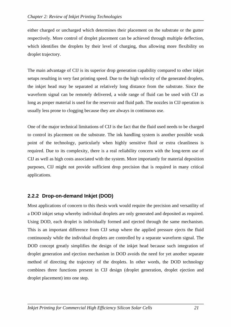
2.2.2 Drop-on-demand Inkjet (DOD).................................................................... 21
2.3 The Inkjet System..................................................................................................... 25
2.3.1 Printhead....................................................................................................... 25
2.3.2 Fluid ............................................................................................................. 30
2.3.3 Substrate ....................................................................................................... 34
2.4 Inkjet Applications in Solar Cell Fabrication........................................................... 36
2.5 Summary .................................................................................................................. 38
Chapter 3 : Dielectric Patterning Using Inkjet ................................................................... 39
3.1 Introduction .............................................................................................................. 39
3.2 Fluid Selection and Formulation .............................................................................. 39
3.2.1 Fluid-Printhead Compatibility Evaluation ................................................... 40
3.2.2 Effects of Fluid on Substrate Surface........................................................... 42
3.2.3 Fluid Jetting Optimisation............................................................................ 49

Table of Contents
Inkjet Printing for Commercial High Efficiency Silicon Solar Cells x
3.3 Process Development and Characterisation ............................................................. 55
3.3.1 Formation of Hole and Line Patterns ........................................................... 59
3.3.2 Effects of Resin Thickness on Feature Sizes ............................................... 60
3.3.3 Effects of Drop Spacing on Feature Sizes.................................................... 63
3.4 Summary .................................................................................................................. 65
Chapter 4 : Device Fabrication Using Inkjet....................................................................... 67
4.1 Introduction .............................................................................................................. 67
4.2 Inkjet Printed High Efficiency Solar Cell Structures ............................................... 68
4.2.1 Selective Emitter .......................................................................................... 68
4.2.2 Localised Contacts ....................................................................................... 71
4.2.3 Surface Texturing and Sculpturing .............................................................. 74
4.2.4 Edge Isolation............................................................................................... 77
4.3 Simple Selective Emitter Solar Cell Using Inkjet .................................................... 80
4.3.1 Device Design .............................................................................................. 80
4.3.2 Device Fabrication ....................................................................................... 83
4.3.3 Device Characterisation ............................................................................... 85
4.4 Summary .................................................................................................................. 88
Chapter 5 : Inkjet Printing of Liquid Dopant Source ........................................................ 89
5.1 Introduction .............................................................................................................. 89
5.2 Direct Inkjet Patterning Concepts ............................................................................ 89
5.2.1 Localised Doping on Silicon Surfaces ......................................................... 89
5.2.2 Simultaneous Patterning and Doping on Dielectric Surfaces ...................... 93
5.3 Jettable Liquid Dopant Sources and Surface Treatment .......................................... 95
5.3.1 Phosphoric Acid-based Liquid Dopant Sources........................................... 95
5.3.2 Specially-formulated Liquid Dopant Sources .............................................. 99
5.3.3 Surface Preparations and Characterisation................................................. 102
5.4 Device Processing Using Direct Inkjet Printing .................................................... 106
5.4.1 Process Development ................................................................................. 106
5.4.2 Device Concept and Fabrication ................................................................ 114
5.4.3 Device Characterisation ............................................................................. 115
5.5 Summary ................................................................................................................ 119
Chapter 6 : Conclusion ........................................................................................................ 120

Table of Contents
Inkjet Printing for Commercial High Efficiency Silicon Solar Cells xi
6.1 Original Contributions............................................................................................ 121
6.2 Future Work ........................................................................................................... 122
References ............................................................................................................................. 125
Appendix A: List of Abbreviations..................................................................................... 138
Appendix B: List of Symbols............................................................................................... 140
Appendix C: List of Printhead Components ..................................................................... 142
Appendix D: Fluid-Printhead Compatibility Test ............................................................ 145
Appendix E: PC1D Modelling Parameters........................................................................ 146
Appendix F: General Approach of Liquid Dopant Formulation .................................... 148
Appendix G: Sheet Resistivity Correction Factor............................................................. 150
Appendix H: List of Author’s Publications ....................................................................... 152

Inkjet Printing for Commercial High Efficiency Silicon Solar Cells xii
This page is intentionally left blank.

Chapter 1: Introduction
Inkjet Printing for Commercial High Efficiency Silicon Solar Cells 1
Chapter 1 : Introduction
1.1 Motivation
For the past two hundred years, global economic growth has been fuelled almost exclusively
by conventional energy sources such as oil, coal and natural gas. Today, about 81% of the
global primary energy supply still comes from these three dominant fossil fuel sources (IEA
2008). Unfortunately, fossil fuels are finite energy sources that are rapidly depleting. The
constant increase in worldwide energy demand continues to outpace the discovery rate of new
reserves and the natural replenishment rate of these resources. Furthermore, greenhouse gas
emissions from the use of fossil fuel have been widely agreed as one of the major contributor
to man-made climate change. Considering these challenges, a more sustainable source of
energy is required as a long term solution to the world’s energy needs.
Electricity is one of the fastest growing end-use of primary energy. According to the
International Energy Agency, about 67% of global electricity generation in 2006 was still
derived from fossil fuel sources (IEA 2008). Almost two-thirds of this electricity was
generated from burning coal, which is one of the most greenhouse gas intensive fuels. In
order to satisfy the ever increasing demand of electricity in a sustainable manner, electricity
generation method needs to gradually shift from polluting fossil fuels to clean renewable fuel
sources.
One of the most attractive renewable electricity generation methods is solar photovoltaics
(PV) technology. The popularity of this technology has been bolstered by recent efforts of
many countries to set up a viable commercial market for solar generated electricity through a
range of government incentives. Consequently, there is currently a very strong demand for
solar cells, which are the building blocks of any solar power products.
Solar cells are devices that directly convert sunlight into electricity. The electricity generated
from solar cells is both clean and renewable because the generation process produces zero
waste and its energy source, sunlight, is virtually inexhaustible. Unlike other methods of
electricity generation, solar cell operation does not involve any moving parts, thus making it a

Chapter 1: Introduction
Inkjet Printing for Commercial High Efficiency Silicon Solar Cells 2
silent and an exceptionally durable system. In practice, many solar cells are usually combined
to form solar modules resulting in a mode of application that is modular and distributed.
Furthermore, solar modules can be well-integrated to the built environment thereby allowing
generation of electricity at the point of use with efficient utility of existing spaces.
Despite having many positive attributes, solar electricity is still more expensive than
conventional electricity in most parts of the world. Although sunlight is readily available for
immediate use at no cost, the solar cells used to convert it into electricity are relatively costly
to produce. One of the biggest cost factors in solar cell production is the raw material. Most
modern solar cells are solid-state devices which are based on the use of a variety of
semiconductor materials. Currently, silicon (Si) – in the form of thin wafers- is, by far, the
most popular semiconductor material used in commercial solar cell production. While Si is
the second most abundant element on earth’s crust (Lide 2008), they mostly occur naturally in
the form of quartz. Solar cell fabrication requires Si with extremely high purity as starting
material and unfortunately, the purification of Si is a very expensive process.
Two other important cost factors in solar cell production are cell conversion efficiency and
manufacturing technology. The economics of solar cell is determined by the amount of
electric power it can generate per unit production cost. The amount of electric power a solar
cell can generate from received sunlight depends on its conversion efficiency. Ideally, a solar
cell is designed to achieve the highest conversion efficiency possible. However, higher
efficiency designs are usually followed by an increase in fabrication complexity and
manufacturing cost. Therefore, improvements in manufacturing technology which can
produce higher efficiency solar cells without an increase in production cost are desirable.
From a technical point of view, further reductions in the cost of solar electricity can only be
achieved by taking into consideration these three key cost factors: raw material,
manufacturing technology and cell conversion efficiency. The present trend in solar cell
manufacturing is moving towards the use of thinner Si wafers and the development of higher
conversion efficiency solar cell designs. In order to realise both objectives in a large-scale
production environment, a suitable manufacturing technology that can produce high
efficiency structures and handle thin Si wafers without compromising production yield also
needs to be developed.

Chapter 1: Introduction
Inkjet Printing for Commercial High Efficiency Silicon Solar Cells 3
1.2 Industrial Screen Printed Silicon Solar Cells
Currently, the industrial production of solar cells is dominated by the screen-printed solar cell
technology. The success of this technology within the present solar industry stems from the
fact that it can achieve reasonably good conversion efficiency through simple manufacturing
processes that are applicable to both monocrystalline and the lower-cost multicrystalline Si
wafers. The screen-printed solar cell technology was first developed in the 1970s, but since
then has improved significantly in terms of its processing technology and final conversion
efficiency. The wide availability of relatively cheap, standardised manufacturing equipments
combined with mature understanding of the technology makes this technology highly suitable
for large-scale production of solar cells.
Almost all screen-printed solar cells in commercial manufacturing uses p-type Czochralski
(CZ) or multicrystalline Si wafers as substrate with general thickness between 210 - 250 μm.
After surface chemical cleaning and random pyramid texturing, the Si wafer surface is
thermally diffused by n-type impurities such as phosphorus in a high temperature furnace to
form the p-n junction. Following an edge isolation process to remove excess phosphorus
diffusion on the edges of the wafer, silicon nitride (SiNx) layer is deposited on the front
surface of the solar cell for both surface passivation and anti-reflection coating (ARC).
Finally, full-surface aluminium (Al) and silver (Ag) finger grid patterns are screen printed on
the rear and front surface of the solar cell respectively, followed by a quick metal co-firing in
a belt furnace to form a back surface field (BSF) and good ohmic contact between both metals
and the Si. A schematic of a typical screen printed solar cell design is shown in Figure 1-1.
Figure 1-1: Schematic of the screen-printed solar cell design (Green 1995).

Chapter 1: Introduction
Inkjet Printing for Commercial High Efficiency Silicon Solar Cells 4
Due to the simplicity of its design, the conversion efficiency of screen-printed solar cells is
fundamentally limited to around 17.0% for monocrystalline CZ Si wafers and 16.0% for
multicrystalline Si wafers. One of the main weaknesses of the screen-printed solar cell lies in
the front surface design. In order to let maximum amount of light into the solar cell, the metal
finger grid on the front surface must be designed to cover the smallest area possible. To retain
sufficient reliability and yield in the screen printing process, the minimum width of these
metal fingers are generally limited to around 120 μm. Therefore, it is necessary for the wide
metal fingers to be separated far enough, usually around 3 mm apart, so that light can enter
the solar cell without too much shading loss.
Such widely separated metal fingers also necessitate higher lateral conductance on the top
surface of the solar cell so that current can laterally flow with minimal resistive loss to the
metal fingers. Consequently, the emitter layer of screen-printed solar cells normally has to be
diffused fairly heavily to achieve a sheet resistance of around 40 - 50 Ω/. As a result of the
heavily diffused emitter, minority carrier lifetime within this layer is significantly reduced
resulting in low spectral response for the strongly-absorbed short-wavelength photons. These
constrains translate to reduced voltage, current and fill factor of the device which result in
limited maximum conversion efficiency achievable by the screen-printed solar cell design.
As the trend towards the use of thinner Si wafers in manufacturing continues, another
impending limitation is the screen printing process itself. Screen printing is a contact process
that subjects the Si wafer to significant mechanical pressure. Thinner Si wafers will be more
fragile and have less tolerance to such pressure, resulting in increased breakage rate. In
addition, the production cost of solar cells strongly correlates to the number of solar cells
produced rather than the size of each individual solar cell. Therefore, the problem with
reduced mechanical strength in thin Si wafers is further exacerbated by the tendency for
manufacturers to use larger area Si wafers.
It is clear that further cost reductions in solar cell production must come from cell designs
with conversion efficiency higher than screen-printed solar cells without incurring significant
cost increase. Many high efficiency solar cell concepts have been previously demonstrated in
the laboratory and several of them have been successfully adapted to large-scale production.

Chapter 1: Introduction
Inkjet Printing for Commercial High Efficiency Silicon Solar Cells 5
1.3 High Efficiency Silicon Solar Cells
The current record for the highest confirmed efficiency of crystalline Si solar cell is 25.0%
held by the University of New South Wales, Australia using the Passivated Emitter and Rear
Locally-diffused (PERL) cell technology (Green et al. 2009). A schematic of the PERL cell
design is shown in Figure 1-2.
Figure 1-2: Schematic of the Passivated Emitter Rear Locally-diffused (PERL)
solar cell design (Zhao et al. 1997).
The PERL cell design incorporates many high-efficiency solar cell structures. The front
surface of the solar cell is textured using inverted-pyramid structures and covered with
double-layer ARC resulting in extremely low front surface reflection. The front metal finger
grids are precisely defined by photolithography to be very thin as to minimise metal shading
loss. Both inverted-pyramid texturing and fine metal fingers significantly reduce the optical
losses which translate to higher current for the solar cell. The PERL cell also features highly-
defined selective emitter structure that minimise both contact resistance and contact area
recombination in heavily diffused regions underneath the metal contacts while the rest of the
top surface is lightly diffused to maintain excellent spectral response on the short-wavelength
photons. Combined with excellent oxide-based passivation on both surfaces of the solar cell,
chlorine-based high lifetime processing and the use of high quality float zone (FZ) Si wafer,
the voltage of the PERL cell is also appreciably increased. The higher voltage and current of
PERL solar cell design together with very high fill factor result in approximately an 8%
absolute improvement in efficiency compared to standard screen-printed solar cells.

Chapter 1: Introduction
Inkjet Printing for Commercial High Efficiency Silicon Solar Cells 6
Despite the high conversion efficiency, the materials and processes required to fabricate the
PERL cell is prohibitively expensive and complicated. PERL cell uses high-quality costly FZ
Si wafers as the substrate material. The fabrication of high efficiency structures such as
inverted-pyramid texturing, highly-defined selective emitter, high-quality SiO2 passivation,
rear locally diffused passivation and point contacting all require multiple long high
temperature and photolithographic-based patterning processes which are both low-throughput,
low-yield and expensive. Furthermore, the vacuum evaporation method of applying ARC and
metal contact in PERL cell fabrication is slow and unsuitable for large-scale production.
A low-cost adaptation of the PERL cell is the Buried Contact (BC) solar cell technology.
While many variants of BC cell design exist, the single-sided BC solar cell design is one that
has been proven suitable for large-scale production with conversion efficiencies of up to
18.3% demonstrated at BP Solar pilot line (Bruton et al. 2003). The single-sided BC cell
design retains many high efficiency features of the PERL cell, especially on the front surface
such as selective emitter structure, isolation of metal-semiconductor contact regions through
heavy diffusions, textured surface, good front surface passivation and the use of narrow but
deep conductive metal fingers. The required patterning processes are substantially simplified
by replacing photolithographic processes with laser scribing. A schematic of the single-sided
BC cell design is shown in Figure 1-3.
Figure 1-3: Schematic of the single-sided Buried Contact (BC) solar cell design
(Green 1995).

Chapter 1: Introduction
Inkjet Printing for Commercial High Efficiency Silicon Solar Cells 7
Further simplification of the BC technology is realised through Laser Doped (LD) solar cell
technology. The main advantage of LD technology is the simultaneous dielectric patterning
and contact region diffusion achieved through laser melting process. Such process
combination saves significant processing time and equipment requirements compared to the
separate process needed in the fabrication of BC solar cell. As a result, the LD technology is
much more attractive for large-scale manufacturing of high efficiency Si solar cell than the
BC technology. A number of solar cell manufacturers have implemented the LD technology
in pilot line production with demonstrated efficiencies of up to 17.5% (Tjahjono et al. 2007).
Besides PERL cell-based solar cell structures, there are other high efficiency Si solar cell
designs such as the backside point-contact solar cell fabricated at Stanford University with
highest confirmed efficiency of 22.7% (Sinton and Swanson 1990). This solar cell design was
originally developed for concentrator cell applications. A schematic of the backside point-
contact solar cell is shown in Figure 1-4.
Figure 1-4: Schematic of the backside point-contact solar cell design (McIntosh
et al. 2003).
Similar to the PERL cell, the backside point-contact solar cell also uses high-quality
expensive FZ Si wafer as the starting material. The use of FZ wafer is even more crucial for
this particular cell design since the collecting junction is located at the rear side of the solar
cell. This requires either higher lifetime material or thinner Si wafers in order for most
carriers generated on the front surface of the solar cell to travel to the rear to be collected by
the junction. The absence of metal grid on the textured and AR-coated front surface
significantly boosts the current of the backside point-contact solar cell. Well-defined thin
interdigitated rear metal interconnection combined with heavy diffusions underneath each
Chapter 1: Introduction
Inkjet Printing for Commercial High Efficiency Silicon Solar Cells 8
polarity of metal contact ensures minimal series resistance. Finally excellent passivation on
both surfaces, the use of front surface field to shield carriers from high front surface
recombination and isolation of high recombination metal-semiconductor contact regions with
heavy diffusions give sufficiently high voltage for this solar cell design. Despite utilising
considerably different design approach from the PERL cell structure, many of the
fundamental high efficiency features that require photolithographic patterning are similarly
present on both PERL and backside point-contact solar cell designs.
In recent years, SunPower Corporation has been commercialising the backside point-contact
solar cell design and putting the technology into large-scale production (Mulligan et al. 2004).
A number of process simplifications were implemented, particularly in the replacement of
photolithographic patterning with screen printing processes. This switch originally resulted in
substantial increase in feature sizes from 5 to 200 μm with a reported corresponding decrease
of 1.5% absolute in average efficiency. Through further optimisation of design parameters
such as diffusion width, metal finger pitch and reduction in cell thickness, SunPower has
reported that large-area backside point-contact solar cells with efficiency of around 22% using
FZ Si wafers should now be achievable in large-scale production (De Ceuster et al. 2007).
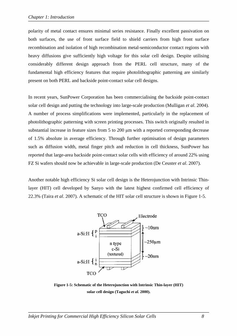
Another notable high efficiency Si solar cell design is the Heterojunction with Intrinsic Thin-
layer (HIT) cell developed by Sanyo with the latest highest confirmed cell efficiency of
22.3% (Taira et al. 2007). A schematic of the HIT solar cell structure is shown in Figure 1-5.
Figure 1-5: Schematic of the Heterojunction with Intrinsic Thin-layer (HIT)
solar cell design (Taguchi et al. 2000).

Chapter 1: Introduction
Inkjet Printing for Commercial High Efficiency Silicon Solar Cells 9
Unlike other previously discussed high efficiency solar cell designs, the HIT cell attains its
high efficiency using large-area n-type CZ Si wafer, which is of lower quality than FZ Si
wafers. The p-n junction in HIT cell is formed rather unconventionally by depositing a thin p-
type amorphous Si (a-Si) onto the n-type CZ Si substrate with another thin layer of n-type a-
Si deposited at the rear of the substrate. Excellent surface passivation and p-n junction quality
are achieved by inserting a thin layer of intrinsic a-Si layer in between both the p-type or n-
type a-Si and the n-type CZ Si wafer. All depositions of a-Si layers are done using Plasma
Enhanced Chemical Vapour Deposition (PECVD) at temperatures below 200 oC.
The unique design of HIT cell results in exceptionally high voltage due to superior surface
passivation properties. Surface lateral conductivity for current collection is achieved through
sputtering of transparent conducting oxide (TCO). Screen printing of silver paste is used to
form higher aspect ratio metal grids on both surfaces. Through the use of n-type Si wafer and
low temperature processing throughout its entire fabrication steps, high minority carrier
lifetime is retained resulting in significantly higher current of the device. The HIT solar cell
technology is commercialised by Sanyo and is currently in large-scale production.
A summary of typical performance parameters for the range of high efficiency Si solar cell
technologies described in this section in comparison with the dominant screen-printed solar
cell technology is presented in Table 1-1.
Cell Technology Voc
(mV)
Jsc
(mA/cm2)
FF
(%)
η
(%) Reference
Screen-printed 619 34.9 76.0 16.5 (Tjahjono et al. 2007)
PERL 696 42.0 83.6 24.4 (Zhao et al. 1998)
Buried contact 625 36.3 80.6 18.3 (Bruton et al. 2003)
Laser-doped 629 37.1 75.0 17.5 (Tjahjono et al. 2007)
Backside point-contact 680 40.8 79.7 22.1 (Mulligan et al. 2006)
HIT 725 38.9 79.1 22.3 (Taira et al. 2007)
Table 1-1: Comparison of typical performance parameters for different high
efficiency solar cell technologies and commercial screen-printed solar cell
technology.

Chapter 1: Introduction
Inkjet Printing for Commercial High Efficiency Silicon Solar Cells 10
1.4 Traditional Patterning Techniques
Patterning is a key processing technology that is commonly used in both commercial screen-
printed solar cells and high efficiency solar cell designs. The patterning process is usually
employed to selectively deposit functional materials such as dopant or metal on the substrate
surface. Similar to most semiconductor device fabrication, solar cell device performance
strongly correlates with precision in the patterning process. For this reason, photolithography
is the patterning method of choice in the fabrication of the highest efficiency solar cells. A
diagram depicting the photolithographic patterning process flow is shown in Figure 1-6.
Figure 1-6: Diagram of photolithographic patterning process flow (Sze 2002).

Chapter 1: Introduction
Inkjet Printing for Commercial High Efficiency Silicon Solar Cells 11
Photolithography is basically a pattern transfer process. As shown in Figure 1-6, the substrate
is first coated with a light-sensitive liquid known as photoresist and then dried (Step 1). Then,
the photoresist is exposed to ultraviolet (UV) light through a mask containing the desired
pattern (Step 2). Exposure to UV light changes the chemical properties of the photoresist.
Depending on the type of photoresist used, the exposed regions either become removable
(positive photoresist) or hardened (negative photoresist). After exposure, the substrate is then
immersed in a developer solution where either the exposed (for positive photoresist) or the
unexposed (for negative photoresist) areas are removed to reveal the underlying dielectric
layer (Step 3). An appropriate etchant is then used to etch the exposed dielectric layer (Step
4). Finally, the excess photoresist layer is removed from the surface (Step 5).
The main advantage of photolithography in solar cell fabrication is its high resolution
patterning capability. Very fine features can be patterned onto the substrate with excellent
precision and repeatability, therefore allowing localised processing that has been the key in
producing many high efficiency solar cell structures. While photolithography is capable of
patterning sub-micron feature sizes, the requirement for solar cell fabrication does not usually
extend below 1 µm. Moreover, the photolithographic ability to precisely align multiple
patterns is critical for the multiple processing sequences often required in fabricating high
efficiency solar cell devices.
Unfortunately, photolithography is an inherently complicated and expensive process. Each
patterning process involves multiple steps including coating, pre-baking, exposure,
developing, post-baking, etching and photoresist removal. The optical equipments used to
align and expose the photoresist-coated wafer is usually a major capital investment. Different
masks need to be created for each pattern resulting in high upfront cost particularly during
prototyping stage. Coating processes, especially spin coating, results in large wastage as only
a small portion of the deposited photoresist stays on the wafer. Furthermore, due to the
subtractive nature of photolithographic processes, virtually all of the deposited photoresist is
wasted upon removal. Photolithography is also a low-throughput process that requires clean-
room environment and it is not suitable for textured surfaces. While acceptable for use in
laboratory environment where high efficiency is the primary objective, photolithography is
not suitable for mass production of solar cells due to its very high fabrication cost per wafer.

Chapter 1: Introduction
Inkjet Printing for Commercial High Efficiency Silicon Solar Cells 12
Laser is becoming an increasingly important patterning tool in high efficiency solar cell
fabrication. Abbott (2006) and Grohe et al. (2007) provide comprehensive review on the
various ways laser patterning can be used to achieve high efficiency Si solar cell structures.
Some of these applications include laser cutting, scribing, drilling, alloying and doping which
can be applied to a range of relevant materials such as silicon, dielectric and metal layers.
Laser patterning usually involves the application of a narrow monochromatic energised beam
onto a specific region on the substrate that results in either surface ablation or surface melting.
A particularly attractive feature of laser patterning is its ability to form very small features on
the Si wafer surface. Although the achievable minimum feature size is still significantly larger
than photolithography, lasers can easily achieve feature sizes ranging from 10 - 40 μm, which
is sufficient for solar cell processing. These characteristics make lasers very useful for solar
cell processes such as surface sculpting and texturing, dielectric patterning, edge isolation,
selective doping and other localised heat treatments. Moreover, laser patterning is a simple,
low-cost, non-contact process with considerably higher throughput than photolithography.
One major drawback of laser processing for solar cells is the resulting crystallographic
damage on laser-processed regions, which can be detrimental to solar cell performance. Laser
ablation, commonly used in scribing and drilling to form structures such as buried contact or
emitter wrap-through (EWT) has been shown to cause lattice dislocations and deep crystal
defects (Chan 1993). In addition, the laser melting process, commonly used for alloying or
doping, causes significant crystallographic stress due to the rapid heating and cooling
experienced in the processed region (Sugianto et al. 2007).
Some of these laser-induced defects can also propagate further into the Si wafer when
subjected to subsequent long, high temperature processes (Wenham et al. 1997). While such
laser damage could be beneficial for lifetime improvement through gettering (Hayafuji et al.
1981), the resulting defects can cause unwanted shunting effects on some solar cell structures
as demonstrated by Guo et al. (2006) and Sugianto et al. (2007). Another potential
disadvantage of laser patterning is the cost of production-scale laser equipments. Despite
being less expensive than photolithographic equipments, the cost of large-scale laser systems
that are capable of sufficiently high throughput for mass production could still be substantial.

Chapter 1: Introduction
Inkjet Printing for Commercial High Efficiency Silicon Solar Cells 13
Screen printing is currently the lowest-cost, highest-throughput option for solar cell
patterning. It is used widely in solar cell manufacturing mainly for the patterning of front
surface metal contact grids and rear surface metal in commercial screen-printed solar cells.
This method is also used in SunPower’s commercial backside point-contact solar cell as a
replacement for photolithography in defining the contact regions (Mulligan et al. 2004). A
typical screen printing setup consists of a screen frame with stainless steel mesh and pre-
patterned emulsion, a squeegee system and a thixotropic paste. The operation is schematically
depicted in Figure 1-7.
Figure 1-7: Diagram of the operation of a typical screen printing system.
The main disadvantage of screen printing is its inability to produce very fine feature sizes.
The stainless steel mesh diameter and opening are critical parameters that determine the
feature size and the amount of materials that can be deposited onto the substrate. Generally,
smaller mesh diameter produces thinner line width. But it is also more fragile and costly to
produce. To keep cost to a minimum while maintaining quality and reliability, the minimum
screen-printable line width is usually limited to around 120 μm for the typical high volume
solar cell production environment. Finally, as mentioned before, screen printing is a contact
process which applies pressure on the fragile Si wafers, making it an increasingly undesirable
process for thinner Si wafers. Nevertheless, despite the shortcomings of screen printing, this
process is still the preferred patterning method in most manufacturing settings.
Besides photolithography, laser and screen printing, there are other less commonly used
patterning process such as mechanical scribing and masked patterning methods such as
plasma etching or thermal evaporation. Mechanical scribing is a contact process where a
diamond-tipped point or rotating blade is used to scribe the surface of the substrate. While it
is a high-throughput and low-cost method of patterning, it also tends to damage the Si surface.
Emulsion
Squeegee
FramePasteMesh
Substrate

Chapter 1: Introduction
Inkjet Printing for Commercial High Efficiency Silicon Solar Cells 14
Similarly, shadow mask-based patterning such as plasma etching or thermal evaporation is
cumbersome and low-throughput, thus not suitable for large-scale production.
To summarise, Table 1-2 compares five key process parameters of various patterning methods
commonly used in solar cell fabrication that are crucial determinants for the three cost factors
involved in large-scale production of solar cells.
Patterning
Method
Overall
Cost
Minimum
Feature Sizes
Si Crystal
Damage
Process
Throughput
Substrate
Contact Mode
Photolithography High < 1 μm None Low Proximity
Laser Medium ~10 μm Yes Medium Non-contact
Screen printing Low ~150 μm None High Contact
Mech. scribing Low ~35 μm Yes High Contact
Shadow mask Low ~4 μm None Low Proximity
Table 1-2: Comparison of various patterning methods in solar cell fabrication.
As evident from the processing requirements of both industrial screen-printed solar cells and
high efficiency solar cell designs, a patterning method that is suitable for large-scale
production is critical to minimise manufacturing costs. Due to the limitations of screen
printing, the trend towards thinner Si wafers and higher efficiency solar cells necessitate the
development of a suitable substitute patterning method. Ideally, the replacement method
should have the characteristics similar to screen printing as shown in Table 1-2, but capable of
producing much finer feature sizes using a non-contact mode of application.
In this thesis, inkjet printing is proposed as an alternative patterning technology that could
potentially satisfy the requirements set out above. Inkjet printing will be shown to be capable
of producing high efficiency solar cell structures using techniques that cost substantially less
than traditional photolithographic processes. Inkjet is also a non-contact and non-mechanical
process that is suitable for high throughput industrial environment. These attributes makes the
development of inkjet technology very attractive for high efficiency solar cell fabrication.

Chapter 1: Introduction
Inkjet Printing for Commercial High Efficiency Silicon Solar Cells 15
1.5 Thesis Objectives and Outline
The objective of this thesis is twofold: (1) to develop new patterning techniques using inkjet
printing technology and (2) to demonstrate the applicability of these inkjet patterning
techniques in producing various solar cell structures and devices. The structure of this thesis
is designed to chronologically address these objectives as follows:
Chapter 2 begins with a review of the state-of-the-art inkjet printing technology. Following
brief background information on historical inkjet technology development and its various
traditional applications, the chapter presents a detailed description on how different inkjet
mechanisms operate. An inkjet system is usually composed of three main components: (1)
printhead, (2) fluid, and (3) substrate. The relationship between these three constituents and
their importance in developing an inkjet process will be discussed. Finally, a summary of past
and present applications of inkjet printing in solar cell fabrication is given in order to provide
some perspectives on the relevance of the work presented in this thesis.
Chapter 3 details the development of a novel indirect inkjet patterning technique that can be
used to pattern dielectric layers as a direct replacement for photolithographic processes. It
begins by evaluating different fluids that could be used for the purpose of dielectric patterning
and examining their compatibility with the printhead and the substrate in an inkjet system. An
appropriate fluid is selected and optimised for the subsequent process development. The
entire patterning process flow is given with optimisations of various critical parameters in
order to achieve the smallest feature sizes possible.
The main purpose of the work described in Chapter 4 is to apply the indirect inkjet patterning
method developed in Chapter 3 to a working solar cell device. Firstly, the inkjet patterning
technique is shown to be a viable alternative for the fabrication of various high efficiency
solar cell structures that traditionally have been created using photolithography or other
methods, such as the formation of selective emitter structure, localised contacts, surface
sculpting and edge isolation. A simple selective emitter solar cell device is then fabricated as
a tool to demonstrate some of the advantages of using the indirect inkjet patterning method
compared to other methods such as laser patterning or photolithography.

Chapter 1: Introduction
Inkjet Printing for Commercial High Efficiency Silicon Solar Cells 16
Chapter 5 proposes two new concepts of using inkjet printing to selectively deposit liquid
dopant sources as a way to perform direct inkjet patterning on both Si and dielectric surfaces.
Due to the unavailability of suitable fluids, two types of solutions are formulated and
developed for inkjet printing use. In order to prepare the surfaces, several methods of surface
treatment are also developed and discussed. After the completion of the inkjet system
development, a novel direct inkjet patterning process is created using direct deposition of
liquid phosphorus dopant source. Finally, the inkjet patterning process is applied to a solar
cell device fabrication with the aim of identifying the limiting issues and concerns of the
process.
Finally, Chapter 6 summarises the important results of the study and analysis performed in
this thesis. Due to the novelty of the work presented in this thesis, there are numerous
opportunities to further develop the various inkjet patterning methods and innovative device
structures described here. Chapter 6 also proposes several suggestions on the possible
roadmap for future work on these topics.

Chapter 2: Review of Inkjet Printing Technologies
Inkjet Printing for Commercial High Efficiency Silicon Solar Cells 17
Chapter 2 : Review of Inkjet Printing Technologies
2.1 Background
In the past several decades, inkjet technology has revolutionised the printing industry by
providing a new low-cost and flexible method of printing. So far, inkjet technology has been
most successfully implemented in the field of graphic imaging. Recently, there has been an
increasing interest in the emerging area of inkjet material deposition. In this application,
functional fluids can be inkjetted onto various surfaces and substrates. Some examples of
functional fluids include metal inks, conductive polymers, surface coating, proteins and
nanoparticles. The versatility of inkjet is highlighted in a wide range of applications in areas
such as electronics, display, chemical, mechanical, optical and life sciences.
Inkjet can be broadly defined as a process where individual droplets of liquid are ejected
through an orifice in a controlled manner. From a scientific point of view, Rayleigh (1878)
was the first to describe the mechanisms of droplet formation due to the instability of fluid
jets. Rayleigh’s principle was used in several notable early technical developments of proto-
inkjet devices such as the analog jet writing devices of Schröter (1932) and Hansell (1933)
and the Mingograph by Elmqvist (1951), which was one of the first commercial inkjet
products available. These devices generally lack sufficient control of the jetting process.
Moreover, jetting frequency and resolution capability were relatively limited and design
complexities placed many restrictions on device manufacturability and practicality.
The advent of computers in the early 1960s spurred development of inkjet devices as a likely
candidate for generating physical output of computer data. Pond (2000, p. 9-42) provides a
comprehensive review of the historical development of modern inkjet technologies between
the 1960s and 1990s. A general observation of the development trends during these decades
indicates that many of the early research efforts were mostly directed towards improving
control of droplet generation, increasing printing speed and improving the reliability of inkjet
systems through design simplifications. These advancements helped establish inkjet as the
device of choice in many graphic imaging applications.

Chapter 2: Review of Inkjet Printing Technologies
Inkjet Printing for Commercial High Efficiency Silicon Solar Cells 18
As inkjet device technologies mature in recent years, more effort has been directed towards
discovering novel applications of the technology where functional fluids are used instead of
traditional coloured inks. In many of these applications, inkjet technology usually has the
potential to either fabricate new structures that previously cannot be achieved through other
available methods or provide an alternative way of fabricating existing structures with lower
costs. A brief summary of these applications is presented in Table 2-1. The breadth of fluids
that have been deposited using inkjet technology underlines its huge potential for use in solar
cell fabrication.
Field Applications Fluids Examples
Electronics
Memory, RFID
tags, flex/printed
circuits
Metal nanoparticles,
solder, conductive
polymer, liquid silicon
Sirringhaus et al. 2000;
Subramanian et al. 2005;
Shimoda et al. 2006
Display OLED displays,
flexible displays
Nanoparticles,
conductive polymer,
light-emitting dye,
Hebner et al. 1998;
Shimoda et al. 2003;
Arias et al. 2007
Life science
Cell sorting, drug
delivery, tissue
engineering
Proteins (collagen),
DNA, antibodies,
bacteria
Roth et al. 2004;
Sanjana and Fuller 2004;
Henmi et al. 2008
Chemistry
pH sensors,
combinatorial
chemistry, coatings
Photopolymerisable
liquids, polymers,
solvents
Tekin et al. 2004;
Carter et al. 2005;
Morita et al. 2005
MEMS
Actuators, sensors,
cantilevers, micro-
fluidic systems
Metal nanoparticles,
colloids, thiols, solvents
Fuller et al. 2002;
Cooley et al. 2002;
Bietsch et al. 2004
Optics Microlenses,
optical array,
Solvent, epoxy resin,
silica, monomers,
prepolymers
Biehl et al. 1998;
Cox and Chen 2001;
Bonaccurso et al. 2005;
Table 2-1: Emerging inkjet applications in various fields, including the range of
typical fluids used in material deposition technologies.

Chapter 2: Review of Inkjet Printing Technologies
Inkjet Printing for Commercial High Efficiency Silicon Solar Cells 19
The inkjet process possesses many attractive attributes. Firstly, it is a non-contact process,
which is a significant advantage compared to other contact processes. It can be applied to
almost any substrate regardless of its composition, morphology, thickness or other properties.
The deposited droplet sizes are very small, usually in the order of picolitres, with high
precision and reliability. For direct inkjet processes, materials are additively deposited on the
substrate only where required. It produces virtually no material waste and simplifies processes
by reducing the number of process steps. Due to its digital nature, fixed production costs
(such as screens and masks) are eliminated. As a result, the running cost of inkjet processes is
generally lower than other methods. This is particularly beneficial for processes that require
smaller sample runs such as prototyping. Finally, inkjet systems typically require lower
capital expenditure compared with other material deposition equipments.
2.2 The Inkjet Mechanism
By fundamental design and functionality, inkjet technology is usually classified into two
types: continuous inkjet (CIJ) and drop-on-demand (DOD) inkjet. Figure 2-1 depicts the
many variations of both CIJ and DOD mechanisms of depositing droplets.
Figure 2-1: Inkjet technology map adapted from Le (1998).
INKJET TECHNOLOGY
Continuous
Binary Deflection
Multiple Deflection
Hertz Microdot
Drop-on-demand
Thermal
Roof-shooter
Side-shooter
Piezo-electric
Squeeze mode
Bend mode
Push mode
Shear mode
Electro-static
Acoustic

Chapter 2: Review of Inkjet Printing Technologies
Inkjet Printing for Commercial High Efficiency Silicon Solar Cells 20
2.2.1 Continuous Inkjet (CIJ)
As the name suggests, the operation of CIJ depends on the continuous generation of ink
stream from a pressurised fluid reservoir. When the fluid stream reaches a certain critical
length, surface tension forces break up the stream into individual droplets. Rayleigh (1878)
theoretically explained this phenomenon by calculating that such break-up occurs when the
stream length is longer than its circumference due to the instability of the jet stream. In order
to synchronise the droplets, a continuous acoustic waveform signal is introduced onto the
fluid stream by means of a transducer or a resonator. By changing the velocity of the stream
and frequency of the wave signal, the size, volume and distances between droplets can be
accurately controlled.
The ejected droplets then pass through a pair of electrodes where the droplets may be charged.
A high voltage deflection plate is then used to steer the charged droplets to the desired
position either on the substrate or onto a gutter where the unused ink is then recycled back
into the reservoir. Figure 2-2 shows the schematic of a typical continuous inkjet setup.
Figure 2-2: Design schematic of a typical continuous inkjet setup (Pond 2000).
In general, a CIJ setup can consists of either single or multiple jet streams, mostly depending
on the printing speed requirement for the particular process. CIJ setups can also be
differentiated by the deflection method used. Binary deflection identifies the droplets as only
Chapter 2: Review of Inkjet Printing Technologies
Inkjet Printing for Commercial High Efficiency Silicon Solar Cells 21
either charged or uncharged which determines their placement on the substrate or the gutter
respectively. More control of droplet placement can be achieved through multiple deflection,
which identifies the droplets by their level of charging, thus allowing more flexibility on
droplet trajectory.
The main advantage of CIJ is its superior drop generation capability compared to other inkjet
setups resulting in very fast printing speed. Due to the high velocity of the generated droplets,
the inkjet head may be separated at relatively long distance from the substrate. Since the
waveform signal can be remotely delivered, a wide range of fluid can be used with CIJ as
long as proper material is used for the reservoir and fluid path. The nozzles in CIJ operation is
usually less prone to clogging because they are always in continuous use.
One of the major technical limitations of CIJ is the fact that the fluid used needs to be charged
to control its placement on the substrate. The ink handling system is another possible weak
point of the technology, particularly when highly sensitive fluid or extra cleanliness is
required. Due to its complexity, there is a real reliability concern with the long-term use of
CIJ as well as high costs associated with the system. More importantly for material deposition
purposes, CIJ might not provide sufficient drop precision that is required in many critical
applications.
2.2.2 Drop-on-demand Inkjet (DOD)
Most applications of concern to this thesis work would require the precision and versatility of
a DOD inkjet setup whereby individual droplets are only generated and deposited as required.
Using DOD, each droplet is individually formed and ejected through the same mechanism.
This is an important difference from CIJ setup where the applied pressure ejects the fluid
continuously while the individual droplets are controlled by a separate waveform signal. The
DOD concept greatly simplifies the design of the inkjet head because such integration of
droplet generation and ejection mechanism in DOD avoids the need for yet another separate
method of directing the trajectory of the droplets. In other words, the DOD technology
combines three functions present in CIJ design (droplet generation, droplet ejection and
droplet placement) into one step.

Chapter 2: Review of Inkjet Printing Technologies
Inkjet Printing for Commercial High Efficiency Silicon Solar Cells 22
The simplified design of a DOD inkjet head has many advantages. Firstly, fluid use is greatly
conserved since the fluids are only deposited where required and there is a much lower
minimum fluid level required for DOD’s inkjet reservoir. This eliminates the need for a
separate ink recycling system and is particularly attractive for many material deposition
applications where the fluid itself might be expensive or difficult to make. A greater packing
density of multiple printheads is also possible since DOD inkjet heads are usually much
smaller than CIJ setups. Another important advantage is the increased deposition accuracy
which comes from more integrated control of droplet generation and placement with the
addition of a simpler binary electronics (i.e. “print” or “no print”). These factors results in
significantly lower costs and increased reliability for DOD inkjet compared to CIJ.
The two most common types of DOD inkjet head are the thermal inkjet (or “bubble-jet”) and
piezoelectric inkjet. The main differentiating feature between the two types is the way the
droplets are generated. In a thermal inkjet device, a heating element such as a resistor is built
onto the wall of the fluid chambers close to the nozzle orifices and is electrically connected to
a voltage source. As shown in Figure 2-3, there are two designs that are usually employed in
fabricating thermal inkjet printheads based on where the heating element is located: (1) the
roof shooter design, and (2) the edge shooter design. In a roof shooter design, the heating
element sits on top of the nozzle plate parallel to the nozzle orifice, whereas in an edge
shooter design, the heating element is on the side of the fluid chamber perpendicular to the
nozzle orifice.
Figure 2-3: Design schematic of a roof shooter design (left) and edge shooter
design (right) of a thermal inkjet device (Lee 2003).
Chapter 2: Review of Inkjet Printing Technologies
Inkjet Printing for Commercial High Efficiency Silicon Solar Cells 23
During operation, an appropriate voltage pulse is delivered to the resistor which results in
heating. The heat then causes the fluid within immediate vicinity of the resistor to boil and
vaporise. This small volume of superheated fluid creates an expanding bubble (hence the term
“bubble-jet”) which pushes the entire fluid volume and ejects the fluid closest to the nozzle
orifice out. When the voltage pulse is switched off, the fluid inside the chamber then begins to
cool and the vapour condenses back into liquid form. This is a very important action since it
initiates: (1) fluid chamber refill, and (2) droplet formation. Once the fluid chamber is refilled
and the ejected droplet has separated from the nozzle, the device returns to its original state
and is ready to jet the next droplet. Surprisingly, this cycle can be reproduced in a reliable
manner for a very large number of times.
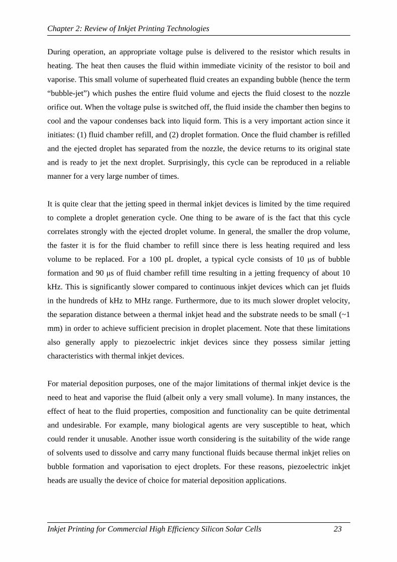
It is quite clear that the jetting speed in thermal inkjet devices is limited by the time required
to complete a droplet generation cycle. One thing to be aware of is the fact that this cycle
correlates strongly with the ejected droplet volume. In general, the smaller the drop volume,
the faster it is for the fluid chamber to refill since there is less heating required and less
volume to be replaced. For a 100 pL droplet, a typical cycle consists of 10 μs of bubble
formation and 90 μs of fluid chamber refill time resulting in a jetting frequency of about 10
kHz. This is significantly slower compared to continuous inkjet devices which can jet fluids
in the hundreds of kHz to MHz range. Furthermore, due to its much slower droplet velocity,
the separation distance between a thermal inkjet head and the substrate needs to be small (~1
mm) in order to achieve sufficient precision in droplet placement. Note that these limitations
also generally apply to piezoelectric inkjet devices since they possess similar jetting
characteristics with thermal inkjet devices.
For material deposition purposes, one of the major limitations of thermal inkjet device is the
need to heat and vaporise the fluid (albeit only a very small volume). In many instances, the
effect of heat to the fluid properties, composition and functionality can be quite detrimental
and undesirable. For example, many biological agents are very susceptible to heat, which
could render it unusable. Another issue worth considering is the suitability of the wide range
of solvents used to dissolve and carry many functional fluids because thermal inkjet relies on
bubble formation and vaporisation to eject droplets. For these reasons, piezoelectric inkjet
heads are usually the device of choice for material deposition applications.

Chapter 2: Review of Inkjet Printing Technologies
Inkjet Printing for Commercial High Efficiency Silicon Solar Cells 24
In a piezoelectric inkjet device, a piezoelectric material is used instead of a heating element to
produce the force necessary to eject a droplet. Piezoelectric materials deform when a voltage
is applied onto them. In an inkjet head, this deformation can be used to displace volume in a
fluid chamber for droplet ejection. Unlike thermal inkjet, the process is purely mechanical and
therefore does not present a hazard to the fluid chemistry. By far, lead zirconate titanate (PZT)
ceramic is the most common piezoelectric material used in the fabrication of piezoelectric
inkjet head. Piezoelectric inkjet operation can be categorized into four types, based on the
PZT deformation mode. In squeeze mode (Figure 2-4(a)) the PZT crystal surrounds the fluid
chamber and “squeezes” it as voltage is applied. In shear mode (Figure 2-4(b)), the applied
voltage is perpendicular to the polarisation of the PZT material. On the other hand, in both
push mode (Figure 2-4(c)) and bend mode (Figure 2-4(d)) the applied voltage is parallel to the
polarisation of the PZT material.
Figure 2-4: Design schematic of a squeeze mode (figure a), shear mode (figure
b), push mode (figure c) and bend mode (figure d) of a piezoelectric inkjet
device - adapted from Brünahl (2003).
(a) squeeze mode (b) shear mode
(c) push mode (d) bend mode

Chapter 2: Review of Inkjet Printing Technologies
Inkjet Printing for Commercial High Efficiency Silicon Solar Cells 25
Due to the use of piezoelectric material as the actuator, the typical piezoelectric inkjet device
design is more complicated and costly to fabricate than thermal inkjet device. It is also more
difficult to miniaturise piezoelectric material in order to produce the smallest droplet sizes and
greater resolution through higher packing density. Nevertheless, for many applications that
require the use of unconventional fluids, piezoelectric inkjet devices are the only choice
because it provides the widest range of fluid formulation possibilities as well as greater ability
to control the droplet formation process through voltage waveform shaping. For these reasons,
in the majority of this thesis work, only the DOD piezoelectric inkjet device is considered for
use.
2.3 The Inkjet System
To successfully develop a new inkjet process, it is important to consider the three key
components of an inkjet system: (1) printhead, (2) fluid, and (3) substrate (Pond 2000). There
is a strong interdependence between these three factors that determines the viability of an
inkjet process. As stated in the thesis objectives, one of the main aims of this thesis work is to
develop a patterning technique that could replace photolithography in high efficiency solar
cell fabrication. The essence of photolithography is pattern transfer, after which a material can
be selectively deposited onto a substrate. In the inkjet case, the central component to achieve
this is the fluid which acts as a medium of transfer. Therefore, for each specific process, a
suitable fluid must be selected or formulated to satisfy the process requirements. It needs to be
realised that the fluid selection or formulation process must also take into account the fluid-
printhead and fluid-substrate interactions. A review of each of this component as they are
relevant to this thesis work will be presented in the following sections.
2.3.1 Printhead
The main inkjet device used in this thesis work is the Dimatix Materials Printer (DMP) from
FUJIFILM Dimatix Inc. It is an integrated inkjet device consisting of cartridge-based
printheads, a substrate platen and a drop watcher system. The printhead used in the DMP is a
DOD piezoelectric inkjet device with two drop volumes available: 1 pL (DMC-11601) and 10
pL (DMC-11610). A photograph of the DMP machine together with the cartridge-based
printhead is available from Dimatix (2008).

Chapter 2: Review of Inkjet Printing Technologies
Inkjet Printing for Commercial High Efficiency Silicon Solar Cells 26
The patent publication by Higginson et al. (2007) discloses the design and construction of the
DMP printer in details. An illustration of the DMP printer design adapted from that patent
document is shown in Figure 2-5.
Figure 2-5: Illustration of the Dimatix DMP machine (Higginson et al. 2007).
In the DMP machine, the substrate is held on the platen by a vacuum and the platen is
movable only in the x direction. The y-axis movement is served by the cartridge mounting
system. It is also possible to adjust the distance between the nozzle plate on the printhead and
the substrate in the z direction. A fiducial camera is attached near the cartridge for alignment
purposes. The positional repeatability of the stage is ±25 μm. The platen can also be heated to
a maximum of 60 oC. A drop watcher camera is integrated into the machine to allow jetting
characterisation through visual checks. The DMC cartridge module has a maximum fluid
capacity of 1.5 mL and is integrated with the printhead module, which can be heated up to 70 oC. The details of its design and construction have been disclosed in Bibl et al. (2006a).
Platen Drop
watcher
Fiducial camera
Cartridge

Chapter 2: Review of Inkjet Printing Technologies
Inkjet Printing for Commercial High Efficiency Silicon Solar Cells 27
The DOD piezoelectric printhead used in the DMP machine operates in bend mode, where the
applied voltage bends the PZT crystal to push the fluid along the pumping chamber and ejects
it out of the nozzles. A schematic cross section of this printhead is shown in Figure 2-6.
Figure 2-6: Schematic cross section of the printhead used for the DMP
cartridge (adapted from Bibl et al. 2005).
For optimal printhead operation, the pumping chamber must first be filled with fluid. It is
critical that the space in the pumping chamber is devoid of any air bubbles because these
bubbles act as a damping agent that will absorb the actuating force of the piezoelectric
deformation. To degas the pumping chamber, the printhead usually needs to be primed before
jetting through a series of fluid purging cycles. During operation, the formation of air bubbles
can be avoided through the use of lung vacuum, which is a basically strong negative pressure
applied to the pumping chamber.
Filtering is another important issue that needs particular attention in miniature devices such as
DOD piezoelectric inkjet printheads. The fluid used must be filtered before being delivered
into the pumping chamber. The reason is because the small channels inside the printhead
construction and the small openings of the nozzle orifice can become easily clogged by large
particles and agglomeration of smaller particles. Printhead clogging due to particles are
usually very difficult to rectify and can be permanent. As a preventative measure, another
filter is also built into the printhead used with the DMC cartridge module.
Ink Flow
Nozzle
Filter Piezoelectric crystal
Pumping chamber
Actuator membrane

Chapter 2: Review of Inkjet Printing Technologies
Inkjet Printing for Commercial High Efficiency Silicon Solar Cells 28
Besides fluid properties (which will be discussed in the next section), the other major factor in
determining the jetting quality is the driving pulse. Some of the parameters that can be
adjusted for optimisation include:
• Jetting voltage – refers to the amplitude of the piezo driving pulse.
• Jetting frequency – refers to the number of cycle of the piezo driving pulse.
• Jetting waveform – refers to the shape and width of the piezo driving pulse.
A typical driving pulse for the DMC printhead is shown in Figure 2-7. The jetting voltage
usually has the most impact in determining whether or not a droplet will eject at its operating
temperature since it affects the degree of the piezo crystal’s deformation. The jetting voltage
also determines the droplet volume and the velocity at which the droplet is ejected. The
quality of the jetted droplet is most affected by the jetting waveform. As shown in Figure 2-7,
the waveform can be divided into three segments. The slew rate and duration of each segment
can be adjusted to achieve the best jetting quality. The slew rate determines how fast the piezo
crystal bends and the duration determines how long it stays in that position. Segment A and
segment B are usually the most influential to jetting quality. In segment A, the piezo crystal
bends such that it creates a negative pressure in the pumping chamber, thus “sucking” the
fluid towards the piezo plate. In segment B, the piezo crystal is driven the opposite way,
creating a force on the fluid volume inside the pumping chamber to push fluid out. Segment C
then controllably reverses the bend to break off the ejected fluid into individual droplets.
Figure 2-7: Typical driving pulse to control jetting in a DOD piezo inkjet head.
Jetti
ng v
olta
ge
Pulse width
A B C

Chapter 2: Review of Inkjet Printing Technologies
Inkjet Printing for Commercial High Efficiency Silicon Solar Cells 29
The jetting frequency then controls how fast the jetting cycle is repeated for a certain period
of time. The higher the jetting frequency, the faster printing speed it can achieve. However, an
increase in frequency usually results in poorer jetting quality, especially for fluids that possess
characteristics further away from the optimal requirements. Since piezo actuation is purely
mechanical, the jetting frequency for DOD piezo inkjet head mostly depends on the time it
takes for the fluid chamber to refill after an ejection event.
Due to the unavailability of the DMP machine with its DMC printheads at that time, some of
the early work for this thesis was performed using other DOD piezo inkjet printheads with
larger nominal droplet volumes from Spectra (former trade name of Dimatix). The two
Spectra printheads used for this thesis work are the Spectra Galaxy PH 256/30 AAA
(“Galaxy”) and the Spectra SX3 (“SX3”). A comparison table between the Galaxy, the SX3
and the DMC printheads are presented in Table 2-2.
Parameter Spectra Galaxy
PH 256/30 AAA Spectra SX3
DMC-11601/
DMC-11610
Number of addressable jets 256 128 16
Nozzle spacing 254 μm 508 μm 254 μm
Nozzle diameter 36 μm 27 μm 9 μm/21.5 μm
Calibrated drop size 28 pL 12 pL 1 pL/10 pL
Adjustment range for drop size 25-30 pL 10-12 pL N/A
Drop size variation 5% <2% 3.5%
Nominal drop velocity 8 m/s 8 m/s 8 m/s
Drop velocity variation 5% ±10% N/A
Operating temperature range Up to 90 oC Up to 70 oC Up to 70 oC
Fluid viscosity range 8-20 cP 10-14 cP 10-12 cP
Compatible jetting fluids Organic solvents, UV curables, aqueous, acidic, basic
Maximum operating frequency 20 kHz 10 kHz 80 kHz
Table 2-2: Product data of the Galaxy, SX3 and DMC printheads (available
from Dimatix 2008)

Chapter 2: Review of Inkjet Printing Technologies
Inkjet Printing for Commercial High Efficiency Silicon Solar Cells 30
The Galaxy printhead was originally designed for industrial graphic printing applications,
whereas the SX3 printhead was specifically designed for high precision industrial material
deposition applications. Both printheads have significantly higher number of nozzles than the
DMC printheads and have a separate fluid handling and supply system consisting of remote
and built-in reservoirs connected by tubings. The nozzle plate of the Galaxy printhead is made
of stainless steel, while the nozzle plates of both the SX3 and the DMC printheads are
fabricated on Si substrates. The design and constructions of the Galaxy have been disclosed
by Moynihan et al. (2004), while the SX3 is MEMS-based printhead similar to those used in
the DMC design (Bibl et al. 2006b).
Both the Galaxy and the SX3 printheads are integrated into a motion precision stage provided
by iTi Corporation (2008). In this case, the substrate platen has a positional repeatability of ±2
μm and can be heated up to 75 oC. In contrast with the DMP system, both the x and y-axis
movement in this system is executed by the platen, while the printhead is stationary. Similar
to the DMC, the jetting temperature may be controlled up to 70 oC for both the Galaxy and
the SX3 printheads and the jetting voltage, frequency and waveform can be separately
adjusted.
2.3.2 Fluid
Before any fluid is loaded into a printhead, the first and foremost consideration must be
whether or not the fluid is compatible with the materials of the printhead construction. In
other words, it must be assured that the fluid does not chemically react with any part of the
printhead that comes in contact with the fluid. This includes the fluid supply and handling
system such as cartridges, reservoirs, tubings and filters. For large-scale industrial
applications, it is particularly important to understand the long term effects of the fluid
compatibility to the printhead because this could determine whether or not the process is
viable for such working environment.
In terms of fluid use, there is a relatively narrow range of fluid properties that can be used in
DOD piezoelectric inkjet device. This is because the mechanical force caused by the
piezoelectric crystal deformation on the fluid is usually quite weak. As a result, the typical
fluid must have sufficiently low viscosity to allow ejection. Viscosity refers to the resistance
of a fluid to flow. In this thesis work, all of the fluids used exhibit Newtonian properties,

Chapter 2: Review of Inkjet Printing Technologies
Inkjet Printing for Commercial High Efficiency Silicon Solar Cells 31
meaning that the flow rate of the fluid is linearly proportional to the force applied to the fluid.
For such Newtonian fluids, the viscosity μ is simply described as:
γτμ&
= (2.1)
where τ is the shear stress, which is the force per unit area required to produce the fluid flow
and γ& is the shear rate, which is the differential velocity of the fluid flow dxdv . The fluid
viscosity can be easily measured using a viscometer.
As shown in Table 2-2, the ideal fluid viscosity range for the three printheads used in this
thesis work is between 8 and 20 cP. If the fluid viscosity is too high, the fluid may not be able
to be ejected through piezo actuation. On the other hand, if the fluid viscosity is too low, the
fluid may drip off the nozzle when idle and may result in poor jetting quality. Viscosity is
usually adjustable by altering the solvent or additive concentrations in the fluid. However,
caution is required in choosing the additives to ensure the functionality of the fluid is not
affected. Moreover, solvents with high boiling point are preferred to avoid excessive
evaporation that could cause nozzle clogging.
Although low viscosity is desirable for jetting purposes, a higher viscosity fluid is usually
preferable to minimise droplet spreading once the fluid lands on the substrate. This is
particularly important for inkjet applications in solar cell fabrication where small feature sizes
are generally more beneficial for the solar cell performance. Fortunately, in many cases,
slightly higher viscosity fluids can easily be modified for jetting through local printhead
heating and still retain its original viscosity as it is ejected and come into contact with the
substrate. It is clear from this discussion that viscosity is one of the most important
considerations in fluid formulation as it affects whether or not a fluid can be jetted.
Another important factor in the jetting viability of a fluid is the size of the particle content of
the fluid. In general, particle size of less than 1 μm in diameter is desirable for jetting using
DOD piezoelectric inkjet device. Particle size becomes more important as the diameter of the
nozzle decreases (for example in the 9 μm-diameter, 1 pL DMC-11601 printhead used in this

Chapter 2: Review of Inkjet Printing Technologies
Inkjet Printing for Commercial High Efficiency Silicon Solar Cells 32
thesis) as it is easier for random group of particles to agglomerate and either clog the nozzles
or cause unreliable jetting. Therefore, it is critical that any particles required to be jetted must
be prepared to sufficiently small size and dispersed and suspended appropriately. It is also
necessary to filter the fluid before loading it into the printhead to remove any particle
contaminants from the fluid.
For most fluids, as long as both viscosity and particle size requirements are met, it should be
possible to jet them using a DOD piezoelectric inkjet device. In addition to these two
properties, surface tension is another important fluid characteristic that must be considered.
Surface tension of a fluid refers to the cohesive internal intermolecular forces within the fluid.
All fluids will naturally try to minimise its surface tension, usually by minimising its surface
area. In a fluid stream, the smallest surface area is usually attained through a spherical shape,
resulting in the characteristic individual round droplets formed when such stream breaks off.
In general the higher the surface tension, the more difficult it is for the fluid to separate from
itself and forms a droplet. However, once a droplet is formed and lands on the substrate, a
high surface tension is desirable since it holds itself well and prevents wetting. If the surface
tension is too low, the fluid might have difficulties in staying together as a droplet and might
separate and form long tails during flight. From jetting perspective, it is also undesirable to
have surface tension that is too low because it increases the possibility of the fluid flooding
the nozzle plate which inhibits good jetting.
For the DOD piezoelectric inkjet devices used in this thesis work, the ideal fluid surface
tension range is around 28-36 mN/m. Surfactants can be used to modify fluid surface tension.
Surface tension can be measured using a number of methods. In this thesis, all the measured
surface tension values were obtained using the Wilhelmy Plate method (Wilhelmy 1863).
More discussions on how surface tension interactions between various phases, particularly
those between the fluid and the substrate will be presented in the next section on substrates.
By ensuring that the fluid formulation results in viscosity, particle content and surface tension
values that are within the ideal range for jetting, a good jetting quality should be achievable
without the need for extensive optimisation of the jetting driving pulse. The aim of any inkjet
process optimisation is to achieve good jetting quality at the highest frequency possible for a

Chapter 2: Review of Inkjet Printing Technologies
Inkjet Printing for Commercial High Efficiency Silicon Solar Cells 33
specific fluid formulation. This will ensure fast printing speed without sacrificing the
precision and reliability of the jetting process. A good jetting quality is usually characterised
by:
• No wetting of nozzle plate during ejection,
• Small jetting drop volume variation from droplet to droplet,
• Uniform droplet velocity from droplet to droplet,
• Absence of satellite droplets,
• Short droplet tail length that joins with the droplet head before it reaches the substrate,
• Straight droplet trajectory between the nozzle and the substrate,
• Long term jetting stability, including during on/off cycles.
Jetting quality characterisation is usually performed visually through the aid of a drop watcher
system. Such system typically would consist of a high speed camera pointed to the nozzle
plate with a backlight for clarity. Some examples of images from a drop watcher showing
various jetting quality issues are shown in Figure 2-8.
Figure 2-8: Drop watcher images of a good droplet formation (figure A),
formation of satellite droplets (figure B), random fluid spray (figure C) and
long tail formation due to low fluid surface tension (figure D) – (Lee 2003).
A B
C D
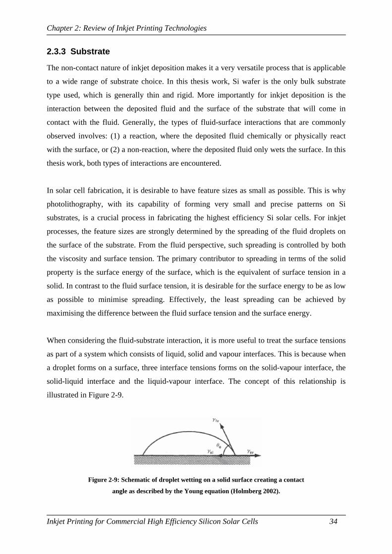
Chapter 2: Review of Inkjet Printing Technologies
Inkjet Printing for Commercial High Efficiency Silicon Solar Cells 34
2.3.3 Substrate
The non-contact nature of inkjet deposition makes it a very versatile process that is applicable
to a wide range of substrate choice. In this thesis work, Si wafer is the only bulk substrate
type used, which is generally thin and rigid. More importantly for inkjet deposition is the
interaction between the deposited fluid and the surface of the substrate that will come in
contact with the fluid. Generally, the types of fluid-surface interactions that are commonly
observed involves: (1) a reaction, where the deposited fluid chemically or physically react
with the surface, or (2) a non-reaction, where the deposited fluid only wets the surface. In this
thesis work, both types of interactions are encountered.
In solar cell fabrication, it is desirable to have feature sizes as small as possible. This is why
photolithography, with its capability of forming very small and precise patterns on Si
substrates, is a crucial process in fabricating the highest efficiency Si solar cells. For inkjet
processes, the feature sizes are strongly determined by the spreading of the fluid droplets on
the surface of the substrate. From the fluid perspective, such spreading is controlled by both
the viscosity and surface tension. The primary contributor to spreading in terms of the solid
property is the surface energy of the surface, which is the equivalent of surface tension in a
solid. In contrast to the fluid surface tension, it is desirable for the surface energy to be as low
as possible to minimise spreading. Effectively, the least spreading can be achieved by
maximising the difference between the fluid surface tension and the surface energy.
When considering the fluid-substrate interaction, it is more useful to treat the surface tensions
as part of a system which consists of liquid, solid and vapour interfaces. This is because when
a droplet forms on a surface, three interface tensions forms on the solid-vapour interface, the
solid-liquid interface and the liquid-vapour interface. The concept of this relationship is
illustrated in Figure 2-9.
Figure 2-9: Schematic of droplet wetting on a solid surface creating a contact
angle as described by the Young equation (Holmberg 2002).

Chapter 2: Review of Inkjet Printing Technologies
Inkjet Printing for Commercial High Efficiency Silicon Solar Cells 35
These three interfaces will always try to minimise its surface energy by changing its effective
surface area in a process more commonly known as wetting. In a wetting process, the
interface where the three surfaces intersect will form an angle known as the contact angle. For
a perfectly homogenous surface, the equilibrium condition at which a contact angle is formed
can be theoretically predicted by Young equation (Young 1805):
lv
slsve γ
γγθ
−=cos (2-2)
where θe is the contact angle and svγ , slγ , and lvγ are the interfacial tensions of the solid-
vapour, the solid-liquid and the liquid-vapour interfaces respectively.
When the contact angle θe is high (e.g. >90o), the surface is said to exhibit non-wetting
properties. In this case, the droplet shape is round and the contact area between the droplet
and the surface is typically very small. On the other hand, when the contact angle θe is low
(e.g. 0o<θe<90o), the surface is said to exhibit partial wetting and the contact area between the
fluid droplet and the substrate surface increases as the contact angle decreases. Finally, if the
contact angle θe is zero, then the surface wets the surface completely and forms a film layer on
the surface.
For a particular solid, a Zisman plot (Zisman 1964) can be constructed which shows the
relationship between the surface tension of a fluid and the resulting contact angle. From this
plot, it is possible to derive the critical surface tension of the solid, which quantifies the
surface tension value of a fluid that would completely wet the surface. Any fluid with surface
tension higher than the critical surface tension will form a droplet and have a contact angle
greater than 0o. It is clear that the critical surface tension value of the solid to be used is
critical in determining the best fluid formulation to achieve as small feature sizes as possible.
It is usually possible to alter the critical surface tension of a solid surface by applying certain
surface coatings or by chemically (surface fluorination) or physically (surface roughness)
treating the surface. In both reaction and non-reaction interactions, it is desirable to have as
low critical surface tension as possible in order to achieve the smallest initial contact area
possible between the deposited fluid and the surface of the substrate.

Chapter 2: Review of Inkjet Printing Technologies
Inkjet Printing for Commercial High Efficiency Silicon Solar Cells 36
2.4 Inkjet Applications in Solar Cell Fabrication
Inkjet printing for Si solar cell processing has been previously investigated as a possible
alternative patterning method. One of the first demonstrated applications was to use inkjet
printing as a substitute for screen printing in applying the front surface metal fingers in
screen-printed Si solar cells. Teng and Vest (1988) developed a jettable Ag-containing
metallo-organic ink and demonstrated its use for front surface metallisation in solar cell. More
recently, similar work has also been pursued by other researchers such as Kaydanova et al.
(2005). Inkjet deposition of metal inks can potentially produce metal line widths as small as
20 µm, which results in significant reduction in shading losses compared to screen printing.
However, the low metal content in the deposited ink and the low aspect ratio of the printed
metal usually limit the conductivity of inkjet printed metal fingers.
To alleviate the conductivity problem, Mette et al. (2007) has recently proposed an alternative
metallisation method based on a combination of printed metal ink and subsequent thickening
of the metal line using light induced plating of copper. In this case, an aerosol jet system was
used to deposit the metal ink instead of an inkjet printer. Nevertheless, the same approach
could theoretically be done with an inkjet printer. Similar plating metallisation method of
nickel and copper has also been applied to other inkjet-structured devices such as those by
Biro et al. (2007) where inkjet is used to deposit masking materials to protect the dielectric
surface from patterning through chemical etching.
Another demonstrated application of inkjet printing for solar cell fabrication is in the
metallisation patterning of crystalline Si on glass (CSG) thin-film solar modules (Green et al.
2004). The inkjet printing process developed for this purpose involves the application of a
low-cost, electrically-insulating resin on the Si surface, followed by inkjet deposition of a
caustic etchant to locally remove the resin in areas where metal contacts are to be made
(Young and Lasswell 2007). Due to the monolithic p+-i-n+ structure, the exposed Si must then
be etched to gain access to the buried n+ layer. After a resin reflow process to avoid shunting,
the inkjet process is repeated to form contacts to the p+ layer. Finally, Al metal is sputtered
onto the patterned surface and isolated using laser. This inkjet metallisation process is
currently used in large-scale production of CSG modules (Basore 2006).

Chapter 2: Review of Inkjet Printing Technologies
Inkjet Printing for Commercial High Efficiency Silicon Solar Cells 37
Besides inorganic solar cells, the inkjet process is also increasingly being utilised in the
fabrication of organic polymer-based solar cells. Such solar cells are usually thin-film devices
whereby suitable soluble polymer blends are applied onto a supporting substrate using
processes such as spin coating or screen printing. An alternative way to deposit such
functional liquid solutions is through inkjet printing. For example, Hoth et al. (2007) recently
demonstrated the fabrication of inkjet-printed organic solar cells with conversion efficiency in
the range of 3%. In this case, inkjet printing is used to coat the glass substrate with a
photoactive layer consisting of jettable polymer-solvent mixture. Konarka Technologies
(2008) have commercialised a flexible solar cell product based on roll-to-roll inkjet
manufacturing process using organic materials.
With the increasing interest in using inkjet as a viable alternative for surface patterning in
solar cell fabrication, there have been many efforts recently to formulate specialty materials
for inkjet deposition. For example, recent publications by Khaselev et al. (2008) and Köhler
et al. (2008) describe the development of a range of jettable materials that are useful for solar
cell fabrication such as improved silver inks, doping inks, diffusion barrier inks and dielectric
etchant inks. Other companies such as Rohm and Haas (2008a) and Filmtronics (2008) have
also developed similar jettable materials for use in solar applications. More novel materials
include Nanosolar’s (2008) CIGS ink that can be printed using roll-to-roll inkjet printer at
very high speed. Besides material development, much has also been done recently in large-
scale industrial inkjet equipment development specifically for solar cell production lines.
Some examples of this include inline inkjet systems from Schmid (2008) and PixDro (2008)
for Si-wafer based solar cells and from Litrex (2008) for thin-film solar cells.
The focus of this thesis work is to develop new inkjet printing processes for high efficiency Si
wafer-based solar cell fabrication, particularly for the purpose of surface dielectric patterning.
There are two approaches introduced in this thesis including a resist-based dielectric
patterning method and a dopant ink dielectric patterning method. Several advantages of the
resist-based method compared to the other available methods are: (1) faster processing time
per wafer, (2) the use of selective emitter structure, (3) smaller feature sizes, (4) high fill
factor contact formation, and (5) reversible process. The dopant ink method has the novelty of
simultaneously forming the heavy diffusion and contact dielectric patterning.

Chapter 2: Review of Inkjet Printing Technologies
Inkjet Printing for Commercial High Efficiency Silicon Solar Cells 38
2.5 Summary
In this chapter, a thorough discussion of the various inkjet printing devices and technologies
currently available has been presented. It has been shown that inkjet devices can be used as
material deposition tools. Its successful applications have been demonstrated in a wide range
of research field. The versatility of inkjet provides a justifiable motivation to explore its
application in fabricating high efficiency Si solar cells.
The two main inkjet mechanisms in the form of continuous and drop-on-demand inkjet have
been reviewed. It has been concluded that the most suitable inkjet device type to use for this
thesis work is the drop-on-demand inkjet. Within the drop-on-demand inkjet technology, the
piezoelectric type is the most desirable for material deposition purposes. This decision is
mainly due to the ability for piezoelectric drop-on-demand inkjet devices to eject a wider
range of fluids and its capability for greater droplet ejection control.
In a typical inkjet system, there are three main components that are interdependent with one
another. They are the printhead, the fluid and the substrate. In a pattern transfer process using
inkjet printing, the fluid is the medium of transfer. As a result, it is important that in the fluid
formulation or choice, the fluid-printhead and fluid-substrate interactions must also be
considered. In this chapter, the significant parameters related to each of these three
components and the relevant background theory has been comprehensively discussed with the
aim of outlining some general guidelines on developing an inkjet process.
Finally, a current survey of the state-of-the-art of inkjet technology applications in solar cell
fabrication has been given. There has been many demonstration of inkjet printing use in
fabricating various solar cell structures with the aim of increasing the efficiency of the device,
simplifying the fabrication process and lowering the fabrication cost. A study of these prior
arts helps identify some novel applications that previously have been unexplored and define
the boundaries for the work performed during this thesis. By reading and understanding the
work presented in the following chapters, it is hoped that the reader will be able to put the
contributions of this thesis in context of the current progress in the inkjet solar cell research.

Chapter 3: Dielectric Patterning Using Inkjet
Inkjet Printing for Commercial High Efficiency Silicon Solar Cells 39
Chapter 3 : Dielectric Patterning Using Inkjet
3.1 Introduction
Inkjet printing has the potential to be a low-cost alternative to photolithographic patterning
methods. The aim is to develop an inkjet printing process that can produce feature sizes
comparable to those that are photolithographically-defined, while retaining the robustness of
the patterning process. This chapter details the development of a novel indirect inkjet
patterning technique which satisfies that aim. It begins by evaluating a range of different
fluids to identify the most appropriate fluid type for dielectric patterning purposes. Some of
the considerations include fluid-printhead compatibility, fluid’s functionality and fluid
jettability. The substrate, where the fluid is deposited, forms the surface area to be patterned
by the inkjet method. In order to achieve as small feature sizes as possible, the interaction
between the fluid and the substrate surface is then investigated. This also helps to narrow
down further the choice of suitable fluid for the process. Finally, an optimisation of the
various jetting controls such as jetting voltage, frequency and pulse length will be shown to
produce a high quality jetting of the selected fluid.
Using the identified fluid-substrate system, an inkjet patterning process flow is developed and
characterised. It will be shown that the inkjet patterning method is able to produce very small
openings in the form of both individual and continuous openings on various dielectric
surfaces relevant to typical crystalline Si solar cell substrates. In addition, an analysis of the
effects of a number of process variables such as platen temperature, resin thickness and drop
spacing on the size of the formed openings is presented.
3.2 Fluid Selection and Formulation
Two of the most widely used dielectric surface materials in industrial solar cell fabrication are
considered throughout this thesis: silicon dioxide (SiO2) and silicon nitride (SiNx). With the
aim of dielectric patterning in mind, the type of fluid that can be used in such a process can be
categorised into:

Chapter 3: Dielectric Patterning Using Inkjet
Inkjet Printing for Commercial High Efficiency Silicon Solar Cells 40
• Direct etching – using fluids that could directly etch the dielectric material.
• Indirect etching – using fluids that could not directly etch the dielectric material but
can be used to pattern an intermediary protective layer.
The former approach involves only the use of a chemical etchant for the specific dielectric
material. The latter approach is analogous to photolithographic process where a protective
layer (e.g. photoresist) is patterned to gain access to the dielectric layer where it could be
exposed to standard dielectric chemical etchants.
The choice of fluid for the simplest process would be to use direct chemical etchant of the
specific dielectric materials. For example, both SiO2 and SiNx could be effectively etched at a
sufficiently high etching rate by a common etchants such as hydrofluoric acid (HF). To a
much lesser extent, sodium hydroxide (NaOH) or potassium hydroxide (KOH) could also be
used to etch both dielectric materials, albeit at much lower etching rate. Another effective
etchant for SiNx is phosphoric acid (H3PO4), although such etching must be performed at an
elevated temperature.
Using the alternative indirect approach, a wide range of fluids can theoretically be evaluated
depending on the masking layer used. Young and Lasswell (2007) demonstrated this concept
by depositing droplets of NaOH using an inkjet system onto a novolac-resin based masking
layer. In this case, the NaOH etches the novolac resin and forms a series of patterned
openings on the masking layer. Kawase et al. (2001) also used a similar concept by using
inkjet to deposit solvent (ethanol) droplets onto polyvinyl phenol (PVP) film to form
openings.
3.2.1 Fluid-Printhead Compatibility Evaluation
The choice of suitable fluid to be used in the inkjet process firstly depends on the fluid’s
compatibility with the printhead used to deposit it. For each of the three printheads used in
this thesis work (see Table 2-2), there exists a Material Compatibility Kit (MCK) available
from the printhead supplier. The MCK contains sample materials, which makes up the
components of the printhead that come in contact with the fluid. Each component’s
compatibility with the fluid is tested by soaking the sample material in the fluid.

Chapter 3: Dielectric Patterning Using Inkjet
Inkjet Printing for Commercial High Efficiency Silicon Solar Cells 41
All the materials present in the fluid path for the Galaxy printhead, the SX3 printhead and the
DMP printheads and the function of each of these components are listed in Appendix C.
These materials also make up the supplied MCK samples to be tested for compatibility with
the fluid. Note that many of the same materials are used in more than one printhead.
The testing method is explained as follows: Before soaking, a baseline weight measurement
of each material was taken. Each material was soaked in the test fluids for seven days and
removed from the fluid solution to be checked daily. The containers used for soaking were
inert to the testing fluid and they were either made of glass or low density polyethylene
(LDPE). Although the actual jetting temperature may be higher, all the soaking tests were
performed at room temperature (25 oC). This was based on the assumption that fluids that are
incompatible at such low temperature were also unlikely to be compatible at higher
temperatures where reaction processes are usually stronger.
Basic evaluation methods involved visual checks and weight measurements of each of the
MCK materials. The short testing timeframe was not intended to simulate use of these fluids
in a large-scale continuous production environment, but rather only for evaluation of
laboratory proof-of-concept experiments. For a fluid to be suitable for laboratory use, it must
not chemically or physically affect any of the MCK materials during the seven-days soaking
period. When changes in the MCK material were observed, an evaluation of the mode of
failure was performed in order to identify the cause.
Many fluids (for both direct and indirect etching) were soak-tested for compatibility with the
printheads without success, especially the corrosive fluids. The compatibility test results of
four particular fluids (with their concentration in w/v) consisting of: (1) HF (49%), (2) NaOH
(50%), (3) acetone (100%) and (4) diethylene glycol (DEG-99%) are listed in Appendix D.
These four fluids represent a range of typical corrosive fluids (acidic HF and basic NaOH)
commonly used for direct etching of dielectric layers and organic solvents for indirect
etching.
The HF solution was found to be particularly damaging to the PZT, Kovar and nozzle plate
materials, while the NaOH solution strongly reacted with the rock trap filter and flex link.
These incompatibilities prevented these two fluids from being used in the Galaxy and SX3

Chapter 3: Dielectric Patterning Using Inkjet
Inkjet Printing for Commercial High Efficiency Silicon Solar Cells 42
printheads. In addition, HF and NaOH are well-known etchants to SiO2 and Si respectively,
which are the main materials used in the nozzle plate construction of the DMP printheads.
Acetone and DEG showed excellent short-term compatibility with all three printheads. The
demonstrated short-term compatibility of both fluids warranted an extended testing period to
evaluate their long-term compatibility. Therefore, an additional three-week soaking of the
components was performed on both acetone and DEG with weekly checking. It was found
that no apparent degradation occurred for the total one-month soaking for all of the tested
printhead components.
From these compatibility experiments, it was concluded that indirect etching methods using
fluids such as acetone and DEG were preferable to direct etching methods which require the
use of corrosive fluids in the printheads used in this thesis work. In addition, the use of highly
corrosive fluids such as HF and NaOH is not desirable due to the safety hazards that they
present, particularly in industrial environments where human operators are routinely exposed
to the chemicals.
3.2.2 Effects of Fluid on Substrate Surface
It is widely known in both semiconductor and photovoltaic manufacturing that certain organic
solutions can be used to remove photoresists. These solvents work by dissolving the resin’s
polymeric bonds under the generally accepted rule that polymers are likely to dissolve in
solvents with similar solubility parameters to its own. The most widely used description of the
solubility parameters was proposed by Hansen (2000). The Hansen solubility parameter is
based on the consideration of three molecular interactions in the material’s molecular
structure consisting of:
• Polar or permanent dipole interactions ( pδ ),
• Non-polar dispersive interactions due to atomic forces ( dδ ), and
• Hydrogen bonding interactions ( hδ ).
For both the polymer and solvent, the coordinate defined by each of these three interactions
can be plotted in a three-dimensional x-y-z graph. For a particular polymer, a spherical

Chapter 3: Dielectric Patterning Using Inkjet
Inkjet Printing for Commercial High Efficiency Silicon Solar Cells 43
volume of solubility can then be created with this point being the centre in addition of another
parameter, the interaction radius R. This solubility sphere determines which solvents can or
cannot dissolve the polymer. Solvents whose point lies inside the solubility sphere are likely
to dissolve, whereas those with points lying outside the sphere are not likely to dissolve the
polymer. These four parameters: pδ , dδ , hδ , and R define the Hansen Solubility Parameters
(HSP) of a particular polymer, which is a useful tool to help predict and choose a suitable
solvent for polymers.
Hansen (2000) formulated a mathematical expression to calculate Ra, which is the distance
between the central coordinate of the polymer solubility sphere and the coordinate of the
solvent’s HSP. In other words, Ra describes the relative position of the fluid’s HSP within the
resin’s solubility sphere. This is shown in Equation (3-1):
212
212
212
2 )()()(4)( hhppddRa δδδδδδ −+−+−= (3-1)
where 1dδ and 2dδ are the dispersive (non-polar) interactions of the respective polymer and
solvent, 1pδ and 2pδ are the polar interactions of the respective polymer and solvent and 1hδ
and 2hδ are the hydrogen bonding interactions of the respective polymer and solvent.
To determine whether or not a solvent is likely to dissolve a polymer, this distance Ra is then
compared with the interaction radius R of the polymer as:
RRaRED = (3-2)
where RED is the relative energy difference between the solvent’s and the polymer’s HSP, Ra
is the distance between the solvent’s and the polymer’s HSP and R is the interaction radius of
the polymer.
The relative energy difference RED is a ratio that indicates the similarity of two molecular
species, such as those between an organic polymer and an organic solvent. A RED ratio
equals to zero implies that the molecules are exactly the same and obviously will be soluble

Chapter 3: Dielectric Patterning Using Inkjet
Inkjet Printing for Commercial High Efficiency Silicon Solar Cells 44
with one another. For RED ratio of less than one but greater than zero, the two organic
molecules display sufficient similarities such that they are likely to be soluble. For RED ratio
approximately equals to one, it implies that the solvent’s HSP is on the boundary of the
polymer’s solubility sphere indicating that it could be partially soluble depending on other
factors. Finally, for RED ratio greater than one, the two molecules have sufficiently different
structure such that they are not soluble with one another.
A special attention must be paid towards the effect of molecular volume on the solubility of
two organic molecules. Smaller molecules are usually more soluble than larger molecules.
This is particularly important for molecules with an RED ratio of or close to one because
solubility could still occur for smaller molecules. Temperature also plays a major role in
determining a solvent’s ability to dissolve polymers. Higher temperatures usually results in an
increase in the solvent’s solubility rate as well as better absorption ability of the polymers for
the solvent (Hansen 2000).
In this thesis work, the chosen masking layer for use in indirect etching is the Microposit
FSC-M surface coating product from Rohm and Haas (2008b). It is a novolac-resin based
coating, which is a similar material used for photoresist without the addition of the
photoactive compounds. Novolac resins are phenol/cresol-formaldehyde polymer with low
molecular weight and phenol to formaldehyde ratio greater than 1. This synthetic resin was
invented by Baekeland (1909) and the chemistry/production of such resin has been described
extensively by Gardziella et al. (2000). It is a common, low-cost resin that has widespread
uses in microelectronics fabrication processes. In this case, the resin is dissolved in propylene
glycol monomethyl ether acetate (PGMEA) solvent at approximately 34% solid content.
The novolac resin has the following HSP correlations: dδ = 20.30, pδ = 15.40, and hδ = 5.30
with an interaction radius R of 15.10 (Hansen 2000). A plot of the novolac resin’s solubility
sphere is shown in Figure 3-1(a). A calculation of the RED values for both acetone and DEG
(listed in Table 3-1) using Equation (3-1) and Equation (3-2) yields 0.72 and 1.15
respectively. This result predicts that acetone is a solvent for the novolac resin whereas DEG
is somewhat not a solvent. Graphically, this is shown in Figure 3-1(b), which is a two-
dimensional pδ vs hδ projection of the three-dimensional Hansen solubility sphere
representation.

Chapter 3: Dielectric Patterning Using Inkjet
Inkjet Printing for Commercial High Efficiency Silicon Solar Cells 45
Figure 3-1: Hansen solubility sphere for novolac resin showing the relative
position of acetone (denoted by ) and DEG (denoted by ) to the sphere
(figure A) and the 2-dimensional δp vs δh projection of the Hansen solubility
sphere showing the relative position of acetone (denoted by ) and DEG
(denoted by ) to the sphere (figure B)
Acetone Diethylene glycol
Molar volume 74.00 94.90
dδ 15.50 16.60
pδ 10.40 12.00
hδ 7.00 20.70
RED value 0.72 1.15
Table 3-1: Hansen parameters of acetone and diethylene glycol (Hansen 2000).
It is useful to note that the exercise above could also be applied to a wide range of other
solvents in order to evaluate their solubility with the novolac resin. Similarly, the Hansen
parameters can also be used to conduct preliminary analysis of a myriad of polymer-solvent
combinations relatively quickly. This is particularly useful to determine the appropriate fluid
and surface type to choose for inkjet process development that involves polymer dissolution
without expending too much time on random approach.
A B

Chapter 3: Dielectric Patterning Using Inkjet
Inkjet Printing for Commercial High Efficiency Silicon Solar Cells 46
Acetone and DEG are examples of a dissolving and a non-dissolving fluid respectively. A
comprehensive review of the theory behind polymer dissolution has been presented by Miller-
Chou and Koenig (2003). When a droplet of solvent comes in contact with a polymer surface,
the solvent diffuses into the bulk of the polymer layer where it disentangles the bonds
between the polymer molecules. For a solvent such as acetone, this action results in the
dissolution of the polymer.
The dissolution of a polymer due to solvent drop has been demonstrated to work very well in
creating structural openings on polymeric surfaces. An excellent example of this application
is the formation of via-holes in all inkjet-printed organic thin film transistors by Kawase et al.
(2001). When a solvent drop is deposited using an inkjet device onto a soluble polymer
surface, a hole with a structure shown in Figure 3-2 is formed.
Figure 3-2: An AFM image of a solvent drop on polymer surface, showing a
characteristic hole shape with high ridges due to the "coffee-ring effect"
(Kawase et al. 2001).
One of the most interesting feature observable for the Atomic Force Microscope (AFM)
image of the hole formation through solvent drop is the presence of high ridges on the edge
surrounding the crater. This is explained by Kawase et al. (2001) as a result of the so-called
“coffee-ring effect” (Deegan et al. 1997). As the inkjet-deposited solvent droplet dissolves the
contacted polymer surface, the dissolved material flows out towards the edge of the droplet
through capillary flow. This is caused by the fact that evaporated fluids on the edge of the
droplet must be replaced by fluid from the centre of the droplet. This flow carries and

Chapter 3: Dielectric Patterning Using Inkjet
Inkjet Printing for Commercial High Efficiency Silicon Solar Cells 47
redeposits the bulk of the polymer material on the edge resulting in the characteristic
peripheral ridge seen in Figure 3-2.
A similar effect was observed when using acetone as a solvent for the novolac resin used in
this thesis work. While the inkjet deposition of solvent is a very elegant way of patterning
surfaces, the small volume of deposited inkjet droplets usually necessitates multiple
depositions at the same location in order for the opening to extend completely through the
polymer layer and to reach the underlying surface. Thicker polymer layers require higher
repetition of solvent deposition. This is a possible disadvantage for the processing throughput
in solar cell fabrication, particularly when applied to large-scale industrial environment.
An alternative approach is to inkjet-deposit a poorly-dissolving fluid such as DEG (as
predicted by its Hansen parameters). In the case of such fluid, the fluid-substrate interaction
involves a plasticising action whereby the fluid selectively weakens some bonds in the
polymer’s molecular structure to effect a change in the material properties. Plasticisers differ
from solvents in that they usually do not cause dissolution of the effected polymer. Therefore,
no holes are formed in the polymer layer. Instead, the plasticiser molecules enter the polymer
layer on contact and push the polymer molecules further apart, sometimes resulting in
swelling or even cracking (Sears and Darby 1982).
For the novolac resin used in this thesis work, DEG was found to be a plasticiser for the
polymer resin. Like most plasticisers, DEG has a higher molecular weight than solvents such
as acetone. DEG also has a RED ratio of more than one, indicating that it is a poor solvent.
When a droplet of DEG is inkjet-deposited onto the novolac resin surface, the DEG droplet
first wets the substrate and then penetrates into the resin to form a plasticised region in the
resin. The size of this plasticised region is strongly dependent on the wetting area. It was
observed that DEG penetration into the resin can be enhanced at higher temperatures. When
the DEG diffuses into the resin, swelling of the resin occurs as the individual resin molecules
are pushed apart by the plasticising DEG molecules. Such swelling is clearly visible from
Figure 3-3, which shows an AFM image of a plasticised region of a novolac resin that was
formed by the inkjet deposition of an 8 pL droplet of DEG.

Chapter 3: Dielectric Patterning Using Inkjet
Inkjet Printing for Commercial High Efficiency Silicon Solar Cells 48
Figure 3-3: An AFM image of an 8 pL plasticiser drop (DEG) on a novolac
resin layer showing the degree of polymer swelling on the surface.
The effect of the DEG on the novolac resin layer is markedly different from that of solvent.
Typically, a cured layer of novolac resin is used as a protective layer against the actions of
acidic etchants such as hydrofluoric acid (HF). When deposition of a solvent such as acetone,
is used to form a hole in the resin, the underlying dielectric layer is directly exposed to the
etching fluid. However, in the case of DEG plasticisation, the weaker bonds in the polymer
molecules allows aqueous etchants such as HF to permeate through the plasticised regions to
access the underlying dielectric without the removal of any resin or the direct exposure of any
dielectric layer. There are several advantages associated with the plasticiser approach such as
potentially smaller feature sizes and the possibility of reversing the permeability of the resin.
It is important to note that the solvent and plasticiser effects described above also apply to
organic fluids other than acetone and DEG. For example, another obvious choice of solvent
would be propylene glycol monomethyl ether acetate (PGMEA), which is the solvent used to
dissolve the novolac resin used in this thesis work. PGMEA and novolac resin has an RED
ratio of 0.95, which indicates that it is likely to dissolve the novolac resin. Other good
solvents for the novolac resin (i.e. those organic fluids with RED ratio less than one) such as
dimethyl sulfoxide (RED ratio of 0.41) and dimethyl formamide (RED ratio of 0.56) would be
expected to have a similar solvent effect too. On the other hand, there are alternative
plasticisers that could be used other than DEG in order to achieve the same plasticising action.
Some examples of such organic plasticisers for novolac resin are triethylene glycol (RED
ratio of 1.06) and propylene glycol (RED ratio of 1.34).

Chapter 3: Dielectric Patterning Using Inkjet
Inkjet Printing for Commercial High Efficiency Silicon Solar Cells 49
3.2.3 Fluid Jetting Optimisation
Table 3-2 shows the fluid properties that are relevant to fluid jetting for both acetone and
DEG. The last column shows the optimum fluid parameters range for the DOD piezoelectric
inkjet printheads used in this thesis work.
Acetone DEG Optimum jetting
Molecular weight 58.08 106.12 N/A
Particle content size (μm) none none < 1.00
Viscosity @ 25 oC (cP) 0.31 27.80 8.00 – 14.00
Surface tension @ 25 oC (mN/m) 22.30 44.80 28.00 – 36.00
Density (g/cm3) 0.79 1.12 > 1.00
Boiling point (oC) 55.10 244.50 > 100.00
Table 3-2: Fluid properties as relevant to jetting for acetone and DEG.
The viscosity of DEG is still higher than optimal. However, the viscosity of fluids can be
reduced to the optimal range by increasing the fluid temperature. This is not true for fluids
having a viscosity lower than the optimum value, such as acetone. In general, surface tension
also decreases with increasing temperature, in which case increasing the jetting temperature of
DEG would also reduce its high surface tension to a value that is closer to optimal. Table 3-2
also shows that the fluid density of DEG is within the optimal range. The DEG fluid also has
a high boiling point, which eliminates potential nozzle clogging and poor jetting caused by
fluid evaporation. Based on the discussion in Section 3.2.2 and the comparison of fluid
properties presented in Table 3-2, it is concluded that DEG is the most suitable fluid.
Despite the non-optimal fluid properties of fluids such as acetone, it is still prudent to realise
that it is possible to modify fluid viscosity and surface tension through the use of additives or
surfactants. Obviously, the used additive must achieve its objective without complications in
terms of printhead compatibility, jetting quality and most importantly, miscibility. In the case
of acetone, a good example of a suitable additive would be DEG, which would increase all of
its important jetting parameters depending on the mixing ratio of the two fluids.
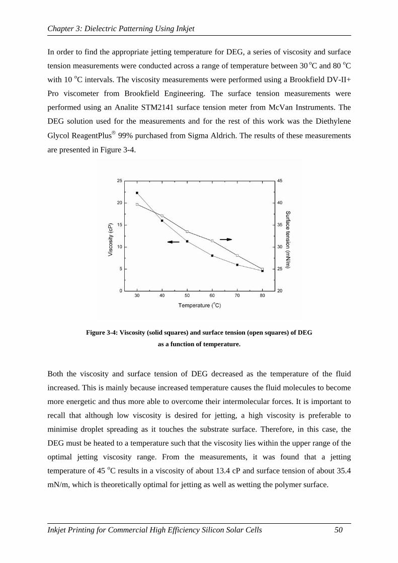
Chapter 3: Dielectric Patterning Using Inkjet
Inkjet Printing for Commercial High Efficiency Silicon Solar Cells 50
In order to find the appropriate jetting temperature for DEG, a series of viscosity and surface
tension measurements were conducted across a range of temperature between 30 oC and 80 oC
with 10 oC intervals. The viscosity measurements were performed using a Brookfield DV-II+
Pro viscometer from Brookfield Engineering. The surface tension measurements were
performed using an Analite STM2141 surface tension meter from McVan Instruments. The
DEG solution used for the measurements and for the rest of this work was the Diethylene
Glycol ReagentPlus® 99% purchased from Sigma Aldrich. The results of these measurements
are presented in Figure 3-4.
Figure 3-4: Viscosity (solid squares) and surface tension (open squares) of DEG
as a function of temperature.
Both the viscosity and surface tension of DEG decreased as the temperature of the fluid
increased. This is mainly because increased temperature causes the fluid molecules to become
more energetic and thus more able to overcome their intermolecular forces. It is important to
recall that although low viscosity is desired for jetting, a high viscosity is preferable to
minimise droplet spreading as it touches the substrate surface. Therefore, in this case, the
DEG must be heated to a temperature such that the viscosity lies within the upper range of the
optimal jetting viscosity range. From the measurements, it was found that a jetting
temperature of 45 oC results in a viscosity of about 13.4 cP and surface tension of about 35.4
mN/m, which is theoretically optimal for jetting as well as wetting the polymer surface.

Chapter 3: Dielectric Patterning Using Inkjet
Inkjet Printing for Commercial High Efficiency Silicon Solar Cells 51
The optimisation of the DEG jetting parameters was conducted using the Dimatix Materials
Printer (DMP). The DMP printer can be operated with printhead cartridges which are capable
of depositing nominally 1 pL and 10 pL droplets. There are slight differences in the jetting
behaviour between the two printheads. For example, higher jetting voltages are usually
required for larger droplet sizes of fluid with the same viscosity and surface tension. In order
to achieve the smallest feature size possible, the 1 pL printhead was used for optimisation.
A 99% DEG solution was loaded into the Dimatix Materials Cartridge (DMC) using a
syringe. The fluid was filtered using a 0.2 μm syringe filter to minimise contamination. The
DMC was then attached to a 1 pL DMC printhead and was left with the nozzles facing down
in air for overnight in order to allow time for the fluid to flow and fill out the chambers inside
the printhead.
The printhead was heated to 45 oC to bring the DEG fluid properties to within the optimal
jetting parameters. Before jetting, the printhead was primed by continuous purging of the
fluid until the fluid was visibly expelled out of the nozzle orifices. Printhead priming is
important to ensure that the fluid level is held by negative pressure just above the nozzle
orifices and that any air bubbles that may have formed inside the pumping chamber while the
printhead was idle are removed.
There are three main jetting parameters that could be adjusted in order to characterise the
droplet velocity: jetting voltage, jetting frequency and jetting waveform. The droplet velocity
can be measured by dividing the distance travelled by the droplet by the time it takes to reach
that distance. In this experiment, all droplet velocity values were measured at a distance of 1
mm from the nozzle, which is also the distance between the nozzle and the substrate. This
gives the droplet velocity at the point of impact. While droplet velocity is quantifiable, the
characterisation of jetting quality is typically more qualitative. The main tool used to
characterise the jetting quality is through visual inspection using the drop watcher system
where jetting properties as described near the end of Section 2.3.2 are desirable.
Due to the optimal fluid properties of DEG at the jetting temperature, optimised fluid jetting
was readily achieved. It was found that the DEG solution could be jetted at a relatively wide
range of jetting parameters. The relationship between droplet velocity and the jetting voltage,

Chapter 3: Dielectric Patterning Using Inkjet
Inkjet Printing for Commercial High Efficiency Silicon Solar Cells 52
jetting frequency and jetting pulse length are shown in Figure 3-5. When the jetting voltage
was varied, both the frequency and the pulse length were kept constant at 5 kHz and 12.8 μs.
When the jetting frequency was varied, both the voltage and the pulse length were kept
constant at 15 V and 12.8 μs. Finally, when the jetting pulse length was varied, both the
voltage and the frequency were kept constant at 15 V and 5 kHz.
Figure 3-5: Droplet velocity dependence on varying jetting voltage (figure A),
jetting frequency (figure B) and jetting pulse length (figure C) for 99% DEG
solution.
Increasing the jetting voltage linearly increased the droplet velocity. This is due to more
bending of the piezoelectric crystal on the application of larger electric field, which causes
more force to be applied on the fluid. It was found that no jetting occurred for voltages below
9.5 V, while droplet quality began to deteriorate for voltages above 19 V (mainly through the
formation of satellite droplets). This is because for voltages below 9.5 V, the actuating force
was simply not strong enough to push fluid out of the nozzle. For voltages above 19 V, it is
likely that the initial part of the droplet was ejected out of the nozzle at a velocity greater than
its tail, resulting in sufficient velocity difference between the two parts of the droplet during
flight such that they separated before they reached the substrate. This is possible due to the
shape of the jetting waveform as shown in Figure 3-6. In segment B, maximum voltage is
applied to the piezoelectric crystal resulting in a maximum actuating force which ejects the
droplet. In segment C, this voltage is scaled back by 40% in order to break off the droplet.
Due to the linear relationship, the droplet velocity resulting from segment C is also about 40%
of segment B. The higher the jetting voltage, the bigger the difference is between the velocity
A C B

Chapter 3: Dielectric Patterning Using Inkjet
Inkjet Printing for Commercial High Efficiency Silicon Solar Cells 53
of the droplet head and the droplet tail. For a substrate distance of 1 mm, 19 V was found to
be the threshold jetting voltage for DEG using this particular waveform where this velocity
difference is such that it would lead to satellite droplet formation.
Figure 3-6: Jetting waveform used to jet DEG in the DMP.
It was found that for a particular voltage, a longer pulse length results in lower droplet
velocity. Note that while varying the total pulse length, the shape and proportion of each
segment of the waveform was maintained as the one shown in Figure 3-6. In general, a shorter
pulse length is desirable since it allows quick recovery of the fluid level inside the pumping
chamber during each jetting cycle, thus allowing higher frequency jetting. However, the pulse
length needs to be long enough so that enough actuation force is delivered to initiate droplet
formation and ejection. For the DEG fluid tested in this experiment, it was found that the
jetting quality began to deteriorate for pulse lengths below 10 μs.
For the jetting frequency, no apparent correlation with the droplet velocity was observed as
the drop velocity stayed virtually constant with increasing frequency. Such behaviour is
expected since a higher frequency only results in faster jetting rate, while each jetting cycle is
still actuated by the same voltage and pulse length. Therefore, jetting frequency variation does
not strongly affect droplet velocity but rather the jetting quality. Higher jetting frequency
typically results in less time for the fluid to reprime itself after each jetting cycle, which is
likely to negatively affect the droplet formation process.

Chapter 3: Dielectric Patterning Using Inkjet
Inkjet Printing for Commercial High Efficiency Silicon Solar Cells 54
Figure 3-7 shows several examples of jetting quality issues encountered during the jetting
optimisation of the DEG solution. In Figure 3-7(a), the droplet did not have a straight
trajectory due to excessively high jetting frequency. In Figure 3-7(b), satellite droplet was
formed due to high jetting voltage. Figure 3-7(c) shows an example of good jetting.
Figure 3-7: Drop watcher images of side-shooting droplet (figure A), satellite
droplet formation (figure B) and excellent jetting quality (figure C).
By combining the analysis presented above, it is concluded that the maximum droplet velocity
can be achieved by jetting at the highest voltage possible without sacrificing jetting quality at
the highest frequency possible while using the shortest pulse length possible. Depending on
the individual nozzles, a jetting voltage of 15-17 V was found to be stable for DEG solution
even for the highest frequency used in this work, which was 20 kHz. The selected pulse
length was 12.8 μs, which gave the required long-term stability in terms of jetting quality. The
resulting average droplet velocity obtained using these parameters were 9 m/s.
A B C
Nozzles

Chapter 3: Dielectric Patterning Using Inkjet
Inkjet Printing for Commercial High Efficiency Silicon Solar Cells 55
After optimisation, excellent jetting quality was observed for the DEG fluid solution jetted
using the parameters described above. Figure 3-8 shows collated time-lapse drop watcher
images of a DEG droplet jetted at 15 V with frequency of 20 kHz and pulse length of 12.8 μs.
The jetting temperature of the DEG was 45 oC.
Figure 3-8: Time-lapse drop watcher images of DEG droplet formation.
The jetted DEG shows all the characteristics of good jetting quality as described in Section
2.3.2. It can be seen that the head of the droplet was smoothly ejected out of the nozzle orifice
followed by an elongated tail that breaks off from the nozzle after 16 μs. The short tail
formation was beneficial as it only took another 15 μs for the tail to join up with the head of
the droplet. The entire droplet was formed within 31 μs of it leaving the nozzle, which is
equivalent to a distance of ~280 μm from the nozzle (assuming 9 m/s droplet velocity). As
evident from Figure 3-7(c), the droplet trajectory was very straight and no satellite droplets
were formed within the distance travelled. Thus, a standard 1 mm distance between the nozzle
and the substrate during printing would be suitable for this work.
3.3 Process Development and Characterisation
In the previous sections, the reasoning for the selection of DEG as the fluid of choice in this
thesis work was discussed by taking into account the various fluid-printhead and fluid-
substrate interactions. The jetting of DEG using an inkjet device was also optimised and
characterised in order to achieve the best jetting performance for the subsequent development
of an inkjet process. In this section, a new and patented inkjet process utilising the plasticising
action of DEG on novolac resin surface for the purpose of dielectric patterning is described.
6 8 10 12 14 16 19 21 23 25 27 29 31 33Time (μs)
Nozzle

Chapter 3: Dielectric Patterning Using Inkjet
Inkjet Printing for Commercial High Efficiency Silicon Solar Cells 56
Figure 3-9: Process flowchart of indirect inkjet dielectric patterning.
A novolac resin layer is applied on both the
top and bottom surfaces of the Si wafer either
by spin-coating or spray-coating. Ideally, the
coating layer needs to be low-cost, easy to
apply and plasticisable by a suitable fluid.
Droplets of DEG are selectively deposited by
inkjet onto the resin layer. DEG plasticises the
resin such that the affected region becomes
permeable to dielectric etchants such as HF.
The regions of the resin not affected by the
DEG maintain its resistance to such etchant.
The substrate is immersed in HF solution,
which allows the etchant to permeate through
the affected regions of the resin and etch the
underlying dielectric layer. The etching time
depends on the etching rate and the thickness
of the dielectric layer.
The resin layer is removed either by wet or
dry etching process or by solvent dissolution.
This exposes the localised Si surfaces on the
patterned dielectric layer.
A Si substrate may have an emitter diffusion
followed by dielectric layer formation such as
SiO2 or SiNx. The dielectric layer enshrouds
the entire surface of the Si wafer.
Chapter 3: Dielectric Patterning Using Inkjet
Inkjet Printing for Commercial High Efficiency Silicon Solar Cells 57
Figure 3-9 shows the flowchart of the entire inkjet patterning process. To demonstrate the
inkjet patterning process, three Si wafers with different types of surface finish were used as
substrates. The three surface finish used in this experiment were: (1) mirror polished surface,
(2) saw-damage-etched surface and (3) random upright pyramid textured surface. Due to its
high reflectivity, the mirror polished surface is preferred for initial optimisation work because
it provides a clear view of the patterned surface under an optical microscope. Both the saw-
damage-etched and the random upright pyramid textured surfaces were selected because they
are commonly-used surfaces in solar cell fabrication.
A thermal oxide was grown on both surfaces of all samples by standard furnace oxidation
process using the wet oxidation method. The thickness of the oxide layer grown for all
samples was between 300-400 nm. Both surfaces of the Si wafers were then coated with the
Microposit FSC-M novolac resin coating (from Rohm & Haas) by spin coating method. The
coating was spun at 5,000 RPM for 30 seconds and then baked in a conventional fan-forced
oven at 140 oC for 10 minutes. The resulting thickness of the resin layer as measured by
Dektak profile was ~2.6 µm thick.
After coating, the wafers were then placed on the platen of the DMP inkjet printer for
printing. The platen was heated to 60 oC to: (1) minimise the contact area between the DEG
droplet and the resin surface when they come in contact with each other and (2) enhance the
DEG diffusion into the resin layer. Since the DEG droplet is absorbed almost instantaneously
on the resin surface, heating the substrate ensures that the surface energy of the resin is kept to
a minimum. Once the DEG droplet begins to diffuse into the resin layer, elevated substrate
temperature helps increase the DEG permeation capability in the resin layer so that the DEG
permeates the entire depth of the resin.
Droplets of DEG were then inkjet-deposited onto the substrate using the jetting parameters as
described in Section 3.2.3. When the substrate was immersed in HF, the etchant would
permeate through the patterned regions of the resin and etch the underlying dielectric layer.
The dielectric etching was achieved without any removal of the overlying resist layer but
rather only through modification of the chemical properties of the resin layer by the
application of the appropriate plasticiser.

Chapter 3: Dielectric Patterning Using Inkjet
Inkjet Printing for Commercial High Efficiency Silicon Solar Cells 58
A swollen region was formed when the plasticising DEG was absorbed by the resin layer as
shown in Figure 3-3. After HF immersion, cracks were formed in this swollen region as
shown in Figure 3-10. One possible explanation for the observed cracking of the resin layer is
the presence of an additional volume in the resin layer caused by the permeation of HF into
the resin layer. The HF molecules is likely to push the resin molecules further apart and
causes further swelling of the polymer up to a point where the polymer surface begins to
crack. This explanation would also provide supporting evidence of the liquid permeation
effect during immersion since the additional volume could only come from the immersion
liquid molecules. The observation of surface cracks after the immersion etching process is
also a good indicator of whether or not the etchants have permeated through the resin layer.
Figure 3-10: Optical microscope image (figure A) and AFM image (figure B) of
the cracked region on the resin surface after HF immersion.
The length of etching time required to completely remove the dielectric layer and expose the
Si surface underneath strongly depended on the etching rate of the solution and the thickness
of the dielectric layer. Once etching was completed, the resin layer was removed by standard
photoresist removal technique. In this experiment, the resin layer was removed using a
Piranha etch solution consisting of a mixture of H2SO4 and H2O2 in a 3:1 ratio. After the resin
was removed, the dielectric layer was patterned with exposed Si surfaces according to the
inkjet printed DEG pattern. The surface was then ready for the next processing step.
10μm
10μm
A B

Chapter 3: Dielectric Patterning Using Inkjet
Inkjet Printing for Commercial High Efficiency Silicon Solar Cells 59
3.3.1 Formation of Hole and Line Patterns
The inkjet patterning method described above can be used to form any pattern on the
dielectric surface including individual hole patterns and continuous line patterns. Both types
of patterns are very useful in creating various high efficiency solar cell structures as will be
described in further detail in Chapter 4. The result of inkjet patterning using the technique
described above is shown in Figure 3-11. The three surface finishes used in this experiment
are polished, saw damage etched and random upright pyramid textured Si wafer surfaces.
Figure 3-11: Optical microscope images of hole and line patterns on mirror-
polished surface (figure A and D), saw damage etched surface (figure B and E)
and random upright pyramid textured surface (figure C and F).
The white-coloured surfaces shown in the optical microscope images in Figure 3-11 indicate
the exposed Si surfaces underneath the SiO2 dielectric layer. It can be seen that only regions
where DEG was deposited became permeable to HF, which etched the SiO2 all the way
through to the Si surface while the rest of the surface was protected by the resin, thus leaving
the SiO2 layer intact (green-coloured surfaces in the optical microscope images).
Although the SiO2 layer in this experiment was grown through oxidation process with a
thickness of approximately 300-400 nm, different SiO2 thickness could similarly be patterned
A B C
D E F
Scale 100μm
Scale 100μm

Chapter 3: Dielectric Patterning Using Inkjet
Inkjet Printing for Commercial High Efficiency Silicon Solar Cells 60
using the same inkjet technique. The same could also be said for SiO2 layers grown through
other methods such as dry oxidation or using spin-on glass. Other dielectric layers commonly
used in solar cell fabrication such as SiNx or TiO2 could also be used instead of SiO2 as long
as the appropriate dielectric etchant is used. In these cases, the only modification required for
the process would be the length of immersion etching required depending on the thickness
and density of the dielectric layer and the etching rate of the etchant solution.
Currently, the smallest feature sizes achievable using this inkjet patterning technique are 30-
35 μm diameter for individual holes and 40-50 μm line width for continuous lines. Figure
3-12 shows an AFM cross section image of an inkjet patterned line on a polished Si surface
similar to the one shown in Figure 3-11(d). In this case, the line width is about 44 μm and the
depth was measured to be about 360 nm, indicating that the SiO2 layer on the patterned region
has been completely removed.
Figure 3-12: AFM cross section image of an inkjet patterned line on a polished
Si surface similar to that shown in Figure 3-11(d).
3.3.2 Effects of Resin Thickness on Feature Sizes
One of the important process parameters that affect the feature sizes produced using this
inkjet patterning method is the resin thickness. Due to the indirect nature of the patterning
method, the way the resin is applied to the surface is crucial because the resin layer is the
actual patterned layer. This means that the inkjet deposited DEG would come in contact and
be functional to the resin layer instead of the underlying dielectric layer. Therefore, the
feature size is expected to have a strong correlation with the thickness of the resin layer.

Chapter 3: Dielectric Patterning Using Inkjet
Inkjet Printing for Commercial High Efficiency Silicon Solar Cells 61
The final thickness of the novolac resin depended primarily on the spin speed and to a lesser
extent, the baking/curing temperature. In general, faster spin speeds result in thinner resin
layers on the substrate surface because more solution is spun off the substrate during the spin-
coating process. Higher baking temperatures or a longer baking time would give thinner resin
layer due to more solvent being evaporated from the coating. It is also worthwhile to note that
other methods of applying the resin can be used, for example through spraying. In this case,
the thickness of the resin can be controlled by adjusting the spraying rate and time.
Figure 3-13 shows the relationship between varying resin thickness and the resulting hole
diameter formed on the dielectric layer for two different printheads. The data represented by
solid squares were obtained using 8 pL droplet volumes, while the data represented by the
solid triangles were obtained using 1 pL droplet volumes. For both sets of data, the substrate
was heated to 60 oC and the droplets were deposited using the jetting parameters as described
in Section 3.2.3. The inkjet patterning process was as described earlier in this chapter. The
pattern printed on the substrate was an array of individual holes separated about 500 μm apart.
Ten random hole diameters were measured on each of the four corners and the centre of the
pseudo-square 8 cm2 polished Si wafer and the average diameter was calculated.
Figure 3-13: Correlation between resin thickness and the resulting hole
diameter produced on the dielectric layer using inkjet deposition of one 8 pL
droplet (solid squares) and four 1 pL droplets (solid triangles) of DEG.

Chapter 3: Dielectric Patterning Using Inkjet
Inkjet Printing for Commercial High Efficiency Silicon Solar Cells 62
From the observed trend as shown in Figure 3-13, it is clear that the resulting hole diameter
decreased as the resin thickness increased for both the 8 pL and 1 pL droplets. A possible
explanation for this correlation is given by considering the DEG absorption mechanism in the
resin layer. Figure 3-14 shows the three possible scenarios of the absorption mechanism of
DEG in the resin layer.
Figure 3-14: DEG absorption mechanism in resin layer showing three possible
scenarios where the resin layer is too thick (figure A), optimal (figure B) or too
thin (figure C). The arrows show the directions in which the DEG diffuses.
When the DEG droplet comes in contact with the resin surface, it is almost instantaneously
absorbed into the resin bulk layer. The width of this region is mostly defined by the area
during the first instance of contact between the DEG droplet and the resin surface. After the
contact area has been defined, the DEG would then diffuse into the resin layer. If the resin
layer is too thick as shown in Figure 3-14(a), there is not enough volume of deposited DEG to
sufficiently plasticise the entire depth of the resin layer. Obviously, thinner resin layers
require less volume of DEG. The diameter of the openings formed using this method is
strongly dependent on the diameter of the droplet. Thus, it is preferable to deposit multiple
droplets of small volume rather than one droplet of larger volume since the nozzle diameter
used to deposit smaller volume droplets is smaller. For example, in this experiment, one 1 pL
droplet was found to be insufficient to plasticise the entire thickness of ~2 µm of the resin
layer. Thus, four layers of droplets had to be deposited in order to provide the required
plasticising volume when using 1 pL droplets. Nevertheless, the small feature size was still
maintained despite the multiple droplet deposition, indicating that the initial droplet-to-
surface contact area is the determining factor for etched hole diameter.
DEG Droplet
Resin layer
Substrate
A
B
C
Plasticised region

Chapter 3: Dielectric Patterning Using Inkjet
Inkjet Printing for Commercial High Efficiency Silicon Solar Cells 63
The trend observed in Figure 3-14 indicates that thinner resin layers results in larger etched
feature sizes. The likely situation in this case is depicted in Figure 3-14(c). Although the resin
layer is thinner, the resin still need to accommodate the same volume of deposited DEG
droplet. Since the DEG does not affect the underlying dielectric layer, the excess DEG must
occupy the lateral volume of the resin layer, which results in wider plasticised region. This
explains why the resulting hole diameter tends to be larger when thinner resin are used.
The optimal situation would be to find a resin thickness that is thin enough so that the
deposited DEG droplet can plasticise the entire depth of the layer without excessive lateral
expansion. This thickness was found to be approximately 2.6 μm for four droplets of 1 pL and
4.6 μm for one droplet of 8 pL. Any layer thicker than these values would not result in
opening formation on the dielectric layer due to the insufficient depth plasticised by the
deposited DEG as shown in Figure 3-14(a). It is also important to realise that these optimal
resin thickness values could change depending on the volume of DEG droplets deposited.
Therefore, the resin thickness would need to be re-optimised for different droplet volumes.
3.3.3 Effects of Drop Spacing on Feature Sizes
The formation of continuous line opening using this inkjet patterning method requires the
joining of individual holes. This means that the each droplet needs to be deposited in
overlapping fashion with its adjacent droplet. As a result of this overlapping, the lines formed
using this method is generally larger in width compared to the diameter of the individual
holes. In order to achieve the smallest line width possible, it is necessary to find the optimal
droplet spacing.
Using the DMP inkjet device, the drop spacing can be easily controlled through the operating
software. This was done by entering the required spacing and adjusting the printhead printing
angle. This printing angle is also known as the printhead sabre angle, which refers to the
specific angle required for the printhead to print at a resolution higher than its native
resolution. The use of sabre angle is particularly important to adjust printing resolution in the
vertical or cross process direction of the printhead.
As previously shown in Table 2-2, the DMC printhead used in this thesis work has a nozzle
spacing of 254 μm, which equates to a native resolution of about 39.4 drops/cm. Since the

Chapter 3: Dielectric Patterning Using Inkjet
Inkjet Printing for Commercial High Efficiency Silicon Solar Cells 64
DEG droplets deposited from a 1 pL printhead resulted in etched holes having a diameter of
approximately 30 μm, overlapping between droplets can only be achieved with a printing
resolution of 333.3 drops/cm or higher. Such higher resolution can be printed by rotating the
printhead and fixing it at an angle that corresponds to the particular required resolution.
In the horizontal (or process) direction, the jetting frequency is critical in determining the
printing speed at the specific printing resolution. At higher resolution, the drop spacing needs
to be smaller which requires the printhead to jet the liquid at higher frequency. If the
maximum jetting frequency is set to a low value (for instance due to poor jetting at higher
frequencies), higher resolution printing would require slowing down the printhead’s
horizontal movement. Thus, a trade-off exists between the drop spacing and the printing
speed for the particular jetting frequency selected in the specific process.
Figure 3-15 shows the correlation between the drop spacing and the resulting final patterned
line width on the dielectric layer. At drop spacing higher than 45 μm, continuous lines ceased
to be formed. The data then shows the increasing separation between individual drops.
Figure 3-15: Correlation between drop spacing and line width and the drop
separation in the case when the drop spacing become to large.
As evident from Figure 3-15, closer spacing between droplets results in wider resulting line
width in the patterned dielectric layer. This is due to the increasing amount of droplet overlap,
which increases the total volume of DEG deposited at a particular spot on the resin layer. If

Chapter 3: Dielectric Patterning Using Inkjet
Inkjet Printing for Commercial High Efficiency Silicon Solar Cells 65
the volume of deposited DEG exceeds the vertical depth absorption capacity of the resin
layer, the plasticiser tends to spread laterally as previously described in Figure 3-14(c) making
the adjacent regions also permeable to etchant solution. With increasing drop spacing, the
overlapping region is also reduced resulting in thinner line width.
However, as the drop spacing is further increased, there will be a point where the droplets
cease to overlap with one another. In this case, the droplets are separated from each other and
results in the standard individual holes with about 30-35 μm diameters. As expected, the
spacing between the droplets continues to increase linearly as the droplets are spaced further
apart.
From these results, it is concluded that assuming the inkjet deposition process is precise, the
optimal drop spacing would be around 40-45 μm. This drop spacing would result in the
narrowest line width. To be conservative however, slightly closer drop spacing was typically
used to offset the possibility of any inaccuracy in drop placement to ensure the printed line is
entirely continuous which is critical for solar cell design and fabrication.
3.4 Summary
In this chapter, a new and patented dielectric patterning technique using an indirect inkjet
printing method was described. The inkjet process development began by evaluating a range
of potential functional fluids in terms of their compatibility with the used inkjet device. The
corrosive nature of many acidic and basic solutions that could be used as direct dielectric
etchants rendered them unusable due to their damaging effects on components of the
printhead. The indirect inkjet patterning process was selected as the most suitable method
given the range of inkjet printheads available at the time. This method is quite similar to the
photolithographic patterning process. However, unlike photolithography, the inkjet process
makes use of low-cost chemicals and equipment to achieve patterning of dielectric layers.
A theory, which uses the HSP to identify solvents for polymers, was described. Using this
theory, DEG was identified as a suitable plasticiser for the novolac resin. It was found that the
inkjet deposition of DEG resulted in plasticised regions in the resin layer, which were
permeable to dielectric etchants, such as HF. These plasticised regions enabled the etching of
Chapter 3: Dielectric Patterning Using Inkjet
Inkjet Printing for Commercial High Efficiency Silicon Solar Cells 66
the underlying dielectric layers. Compared to solvents, some of the advantages of using
plasticisers are: (1) the volume of plasticiser required to form the permeable regions is less
than the volume of solvent required to form openings in the polymer, and (2) compounds that
can act as good solvents for the resin typically evaporate more easily than the higher
molecular weight compounds that act as plasticisers, thus making it less ideal for jetting. The
optimisation of the jetting parameters for DEG was described. It was found that the fluid
properties of DEG were very suitable for jetting, thus making it possible to achieve high
precision deposition by inkjet at relatively high frequency.
Finally, a robust process flow of the indirect inkjet patterning method was described.
Individual round openings with diameters as small as 30-35 μm and continuous line patterns
with width as narrow as 40-50 μm on 300-400 nm thick SiO2 layer were shown to be
routinely reproducible using this inkjet patterning method. In order to achieve the smallest
possible feature sizes, two important parameters: (1) resin thickness and (2) drop spacing
were optimised. The development steps involved in formulating and optimising this inkjet
patterning process are applicable to the development of other inkjet patterning processes. As
will be shown in the following chapter, this new indirect inkjet dielectric patterning process
can be very useful to solar cell fabrication.

Chapter 4: Device Fabrication Using Inkjet
Inkjet Printing for Commercial High Efficiency Silicon Solar Cells 67
Chapter 4 : Device Fabrication Using Inkjet
4.1 Introduction
Many higher efficiency Si solar cell designs have been proposed and developed over the
years. Some of the notable designs were discussed in Section 1.3. The final conversion
efficiency of a solar cell is determined by the total recombination, current generation and the
parasitic losses of the device. The relationship between these three device parameters is
summarised in Equation (4-1):
FFJV scoc ××=η (4-1)
where η is the solar cell conversion efficiency, Voc is the open-circuit voltage of the solar cell,
Jsc is the short circuit current of the solar cell and FF is the fill factor of the solar cell.
The open-circuit voltage (Voc) of the device is related to the total recombination in the device.
High voltages can be achieved by maintaining good minority carrier lifetime, excellent
surface passivation and minimum dark saturation current.
The short-circuit current (Jsc) of the device is related to the current generation in the device,
which in turn is determined by light absorption. Strategies to enhance light absorption include
the use of surface texturing, light trapping, anti-reflection coating and reducing front surface
shading.
The fill-factor (FF) is a measure of parasitic losses in the device. These losses can be in the
form of either shunt or series resistances, which typically manifests themselves within the
metal contact regions of the solar cell.
This chapter will show how the indirect inkjet patterning method developed in Chapter 3 can
be used to form a range of structures that maximises the Voc, Jsc and FF (and therefore the
conversion efficiency) of the solar cell. In addition, working solar cell devices that incorporate
several of these high efficiency structures are fabricated and analysed.
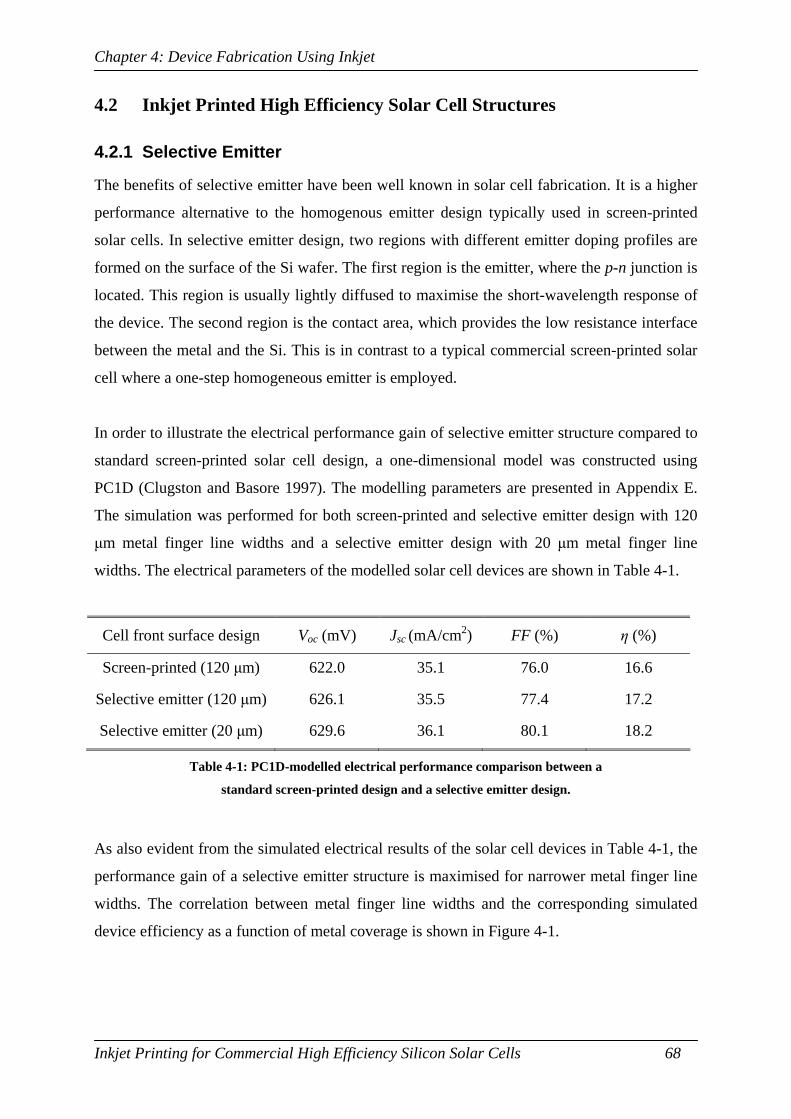
Chapter 4: Device Fabrication Using Inkjet
Inkjet Printing for Commercial High Efficiency Silicon Solar Cells 68
4.2 Inkjet Printed High Efficiency Solar Cell Structures
4.2.1 Selective Emitter
The benefits of selective emitter have been well known in solar cell fabrication. It is a higher
performance alternative to the homogenous emitter design typically used in screen-printed
solar cells. In selective emitter design, two regions with different emitter doping profiles are
formed on the surface of the Si wafer. The first region is the emitter, where the p-n junction is
located. This region is usually lightly diffused to maximise the short-wavelength response of
the device. The second region is the contact area, which provides the low resistance interface
between the metal and the Si. This is in contrast to a typical commercial screen-printed solar
cell where a one-step homogeneous emitter is employed.
In order to illustrate the electrical performance gain of selective emitter structure compared to
standard screen-printed solar cell design, a one-dimensional model was constructed using
PC1D (Clugston and Basore 1997). The modelling parameters are presented in Appendix E.
The simulation was performed for both screen-printed and selective emitter design with 120
μm metal finger line widths and a selective emitter design with 20 μm metal finger line
widths. The electrical parameters of the modelled solar cell devices are shown in Table 4-1.
Cell front surface design Voc (mV) Jsc (mA/cm2) FF (%) η (%)
Screen-printed (120 μm) 622.0 35.1 76.0 16.6
Selective emitter (120 μm) 626.1 35.5 77.4 17.2
Selective emitter (20 μm) 629.6 36.1 80.1 18.2
Table 4-1: PC1D-modelled electrical performance comparison between a
standard screen-printed design and a selective emitter design.
As also evident from the simulated electrical results of the solar cell devices in Table 4-1, the
performance gain of a selective emitter structure is maximised for narrower metal finger line
widths. The correlation between metal finger line widths and the corresponding simulated
device efficiency as a function of metal coverage is shown in Figure 4-1.

Chapter 4: Device Fabrication Using Inkjet
Inkjet Printing for Commercial High Efficiency Silicon Solar Cells 69
Figure 4-1: PC1D-modelled selective emitter cell efficiency as a function of
metal coverage percentage area for different metal finger line widths. The data
points represented by solid squares show the optimal metal coverage
percentage for each line width and its corresponding maximum cell efficiency.
There are several reasons for the observed increase in maximum device efficiency as the
metal finger line width is reduced. Firstly, narrower line widths allow the metal fingers to be
spaced closer to each other, which reduce the lateral series resistance in the emitter. Secondly,
closely-spaced fingers reduce the metal coverage area which improves light absorption
through less shading of the front surface. Finally, lower metal coverage area means increased
passivated surface area and less dark saturation current contribution from the metal-Si
interface regions. Therefore, to achieve the highest efficiency possible in a selective emitter
structure, it is preferable to use a patterning method that is capable of producing very fine
feature sizes.
The formation of selective emitter using indirect inkjet patterning method follows similar
processing steps as a photolithographically defined selective emitter. Typically, after a light
emitter is formed in the first diffusion step, a dielectric layer is applied on the front surface of
the solar cell. The dielectric layer serves as a diffusion mask for the subsequent heavy
diffusion process. Dielectric patterning steps as described in Figure 3-9 is then followed to
form the desired contact pattern on the Si surface. Finally, a second high temperature furnace

Chapter 4: Device Fabrication Using Inkjet
Inkjet Printing for Commercial High Efficiency Silicon Solar Cells 70
diffusion step is performed to form heavy diffusion regions on the patterned contact areas.
This processing method produces heavily doped contact lines of 45-50 μm widths with sheet
resistivities as low as 5 Ω/, thus allowing low metal coverage area and low contact
resistance.
One way to monitor the effects of the inkjet-formed selective emitter process on the device
quality is through its minority carrier lifetime which was measured using the flash photo-
conductance technique (Sinton and Cuevas 1996). A batch of ten standard commercial CZ, 1
Ω.cm, p-type Si wafer were alkaline-textured followed by a phosphorus thermal diffusion to
form a 100 Ω/ emitter and growth of a 350 nm thermal oxide. The front surface of the
wafers were then inkjet patterned and the wafers then underwent a second heavy phosphorus
thermal diffusion following the procedure described in the previous paragraph to create the
selective emitter structure. Average implied Voc of 664.1 mV and 662.7 mV were measured
after the first and second high temperature processes respectively, indicating that high bulk
lifetime and low surface recombination were maintained during the inkjet selective emitter
formation process.
Due to its similarity with the photolithographic patterning process, one of the main
advantages of the said inkjet patterning is the absence of crystallographic damages in the Si
like those commonly found in laser processing. Wenham et al. (1997) have previously studied
the far-reaching effects of laser-induced crystal defects in Si by performing electron-beam
induced current (EBIC) scan that shows subsequent high temperature process during the
heavy diffusion can cause the defects to propagate deep into the Si substrate. A similar
method using EBIC scan was used to demonstrate the inkjet patterning quality. EBIC can
determine the location of the junction in a freshly-cleaved surface by exposing the surface to
electron beams which generate current. However, only the current within the vicinity of the
space charge region in the junction is able to contribute due to very high recombination
elsewhere.
Figure 4-2(a) shows an EBIC scan superimposed with an SEM image of the heavily diffused
region in an inkjet patterned selective emitter structure. The light emitter was diffused with
phosphorus to about 100 Ω/ and the heavy emitter was diffused to about 5 Ω/. For
comparison, Figure 4-2(b) shows the EBIC scan of laser formed groove (Wenham et al. 1997)

Chapter 4: Device Fabrication Using Inkjet
Inkjet Printing for Commercial High Efficiency Silicon Solar Cells 71
Figure 4-2: EBIC images of inkjet selective emitter (figure A) and laser formed
groove - from Wenham et al. (1997) - (figure B). Both underwent heavy
diffusion process after patterning. The well-defined junction location in Figure
A indicates the absence of crystallographic damage in the patterned region.
From Figure 4-2, it is evident that the junction depth was clearly delineated within the reach
of the diffusion process, which indicated the absence of any defects that would have allow the
phosphorus to propagate deep into the substrate. This is in contrary to laser-processed regions
as shown by Wenham et al. (1997) whereby phosphorus was shown to diffuse as deep as 30
μm through the defected region. This comparison shows one of the advantages of forming
selective emitter structure using inkjet patterning.
4.2.2 Localised Contacts
Although most incoming photons in solar cells are absorbed within the first few microns of
entering the device, the rear surface of a solar cell still potentially represents a high
recombination centre that could drag down the device electrical performance. The rear surface
of the solar cell becomes important when it is the dominant recombination region in the
device. Improvements at the rear surface can be achieved through surface passivation together
with the use of a localised contacting scheme.
Some typical designs of well-passivated, localised rear contact structures in the fabrication of
high efficiency Si solar cell together with their typical open-circuit voltage values are shown
in Table 4-2. The dielectric layer used to passivate the rear surfaces in all of these solar cells
was SiO2. The contacting rear metal used was Al and dielectric patterning was done using
photolithography.
Inkjet-formed contact region
A BB 25 μm

Chapter 4: Device Fabrication Using Inkjet
Inkjet Printing for Commercial High Efficiency Silicon Solar Cells 72
Cell Technology Diagram of Rear Surface Design Voc (mV) Reference
PERC
(0.2 Ω.cm,
p-type, FZ)
696 (Blakers et al. 1989)
PERL
(2 Ω.cm,
p-type, FZ)
696 (Wang et al. 1990)
PERT
(1.5 Ω.cm,
p-type, MCZ)
707 (Zhao et al. 2001)
PERF
(1 Ω.cm,
p-type, FZ)
714 (Altermatt et al. 1996)
Table 4-2: Various low-area localised rear contacting schemes used in the
fabrication of high efficiency Si solar cell (the front surfaces are omitted from
the diagrams).
In the PERC structure, the rear comprised of SiO2-passivated p-type surface with
photolithographically defined localised metal directly contacting the substrate. In terms of
passivation quality, the PERL cell was mostly equivalent to the PERC passivation except for
the reduced dark saturation current contribution from the metal contact regions which in
PERL were passivated with heavy boron diffusion. A major improvement in Voc was observed
with the PERF structure through the incorporation of an n-type surface on the rear. This
creates a floating junction structure whereby the rear p-n junction is not contacted to the
external circuit. The high Voc achieved by the floating junction structure can be attributed to
the reduction of hole density in the vicinity of the rear surface in the n-type layer and due to
the superior dielectric passivation quality on an n-type surface compared to a p-type surface.
All of these localised rear contact schemes can be equivalently attained using the indirect
inkjet patterning method by printing and forming individual holes according to a
predetermined pattern throughout the rear surface.
p p++ p++
n+
pp++ p++
p+
p p++ p++
p

Chapter 4: Device Fabrication Using Inkjet
Inkjet Printing for Commercial High Efficiency Silicon Solar Cells 73
In most standard screen-printed solar cell process, the gaseous phosphorus used during
emitter formation usually also result in a rear n-type layer. This unwanted layer is usually
isolated from the front surface either by plasma etching, chemical etching or laser isolation
and then destroyed by screen-printed Al during the metal firing step. However, this n-type
layer could actually be beneficial by using it as a floating junction structure at the rear of the
solar cell as shown in Figure 4-3(a). Passivating an n-type surface using dielectric layer is
much more advantageous than a p-type surface resulting in a lower surface recombination
velocity. Furthermore, minority carriers are less likely to recombine in the bulk area near the
rear surface due to the low hole density within that vicinity.
Once the floating junction structure is set up, dielectric patterning is still required in order to
form localised rear contacting scheme. Indirect inkjet patterning was used to achieve this. In
this case, the n-type layer is the exposed layer on the rear surface while the metal needs to
make contact into the p-type substrate. After the rear dielectric passivating layer has been
patterned, the n-type Si surface is then isotropically etched until the buried p-type layer is
exposed. The isotropic etchant would create an overhanging dielectric structure as shown in
the Focused Ion Beam (FIB) image in Figure 4-3(b). The overhanging dielectric structure is
useful as a mask in a line-of-sight metal deposition to prevent metal from depositing into the
n-type walls. This provides an electrical isolation between the p-type and the n-type layers,
which avoids the shunting problem commonly encountered in PERF solar cells.
Figure 4-3: Floating junction-passivated localised rear contacting scheme (for
clarity, the rear surface is facing up in Figure A). Figure B shows a Focused Ion
Beam (FIB) image of the inkjet-fabricated overhanging dielectric structure.
p
Dielectric layer Aluminium
Silicon Overhanging dielectric
n+
A B
n+

Chapter 4: Device Fabrication Using Inkjet
Inkjet Printing for Commercial High Efficiency Silicon Solar Cells 74
The ability of the indirect inkjet patterning method to create both line and hole openings in
dielectric layer can also be beneficially used to form interdigitated rear contacting scheme.
Such rear contacting scheme alleviates the need for a metal grid on the front surface, thus
resulting in zero shading. The inkjet patterning can be applied multiple times in order to
create the alternating p-type and n-type contact regions on the rear surface. An innovative
application of this indirect inkjet patterning technique on a low-temperature simultaneous
contacting of n-type and p-type surfaces has been demonstrated by Kuepper et al. (2007).
4.2.3 Surface Texturing and Sculpturing
The surface of a bare Si wafer reflects about 30% of the incident light. In order for the Si
material to absorb more photons to generate carriers, more proportion of the incident light
needs to be coupled into the Si. Surface texturing is commonly used to reduce the surface
reflection of Si in solar cell fabrication.
The most common method of surface texturing used in large-scale production is the alkaline-
textured surface, which produces random upright pyramids on the Si surface with dimensions
between 3-8 μm. For high efficiency Si solar cells, other more effective surface texturing
using macrogroove and inverted pyramid structures have been used to further reduce
reflection from the surface of the Si wafer by increasing the number of bounces of incoming
light reflected from the Si surface. This improves the number of chances for the light being
absorbed by the Si as well as increasing the path length of the light inside the wafer due to
favourable incident angles. Comparison of the effectiveness of various textured surfaces for
solar cells has been reviewed by Campbell and Green (1987).
Despite the superior light-trapping properties of macrogroove and inverted pyramid
structures, the formation of such structures requires dielectric masking and photolithographic
patterning. The indirect inkjet patterning process offers an alternative patterning method to
photolithography. Individual closely-spaced holes and continuous lines can be formed on the
dielectric surface of the Si wafer followed by anisotropic alkaline etching to form inverted
pyramid and macrogroove structures respectively. In both cases, the dielectric layer acts as an
important etching mask, which defines the desired surface structures. The resulting inkjet
printed macrogroove and pyramid textured surfaces are shown in SEM images of Figure 4-4.

Chapter 4: Device Fabrication Using Inkjet
Inkjet Printing for Commercial High Efficiency Silicon Solar Cells 75
Figure 4-4: SEM images of indirect-inkjet-patterned macrogroove texturing
(figure A) and inverted pyramid texturing (figure B) on a polished Si surface
(Borojevic et al. 2008).
Compared to photolithographically defined structures, the main limitation of the inkjet printed
texturing is the minimum feature sizes. Another major limitation is the density of the printed
features, which determines how close the spacings between each feature. A typical array of
line patterns used to form macrogrooves such as in Figure 4-4(a) usually requires a minimum
spacing of ~20 μm between the lines. Similarly, the edge-to-edge spacing for hole patterns
like in Figure 4-4(b) is ~30 μm. This limit is imposed by several factors including the inkjet
deposition accuracy, substrate’s surface energy, resin adhesion and etching time.
Excessive space between the surface features causes flat surfaces on the Si wafer which have
poor reflection properties. Therefore, it is preferable to minimise the inter-feature space to
achieve the lowest possible surface reflection. In order to mitigate this issue, Borojevic et al.
(2008) have proposed a possible solution by using isotropic etches after inkjet patterning in
order to undercut the spaces in between features and reduce their effective spacing. This way,
the distance between two adjacent features is no longer limited by the resolution of the
dielectric patterning as a result of the inkjet printing step. The reflectance results of such
inkjet-formed macrogrooves and inverted pyramid structures have been shown to be
comparable to photolithographically-formed inverted pyramids used for the front surface
texturing in the world-record PERL solar cell design (Borojevic et al. 2008).
A B

Chapter 4: Device Fabrication Using Inkjet
Inkjet Printing for Commercial High Efficiency Silicon Solar Cells 76
The inkjet grooving method can also be similarly applied to form grooves in solar cell designs
such as the buried contact solar cell (BCSC). The standard grooves in BCSC have been
formed using laser ablation or mechanical scribing followed by alkaline etching to remove
slags or damage from the process. Alternatively, the indirect inkjet patterning method
combined with chemical etching can be used to form these grooves, which has the advantage
of causing no crystallographic damage to the material.
A particularly interesting application of surface sculpturing is when both sides of the Si wafer
surfaces are covered with macrogroove structures with the macrogrooves in one side of the
surface formed perpendicular to the other side. This so-called perpendicular slat solar cell
structure is shown schematically in Figure 4-5.
Figure 4-5: Perpendicular slat solar cell structure.
In order to form this structure, the inkjet printing method as described in Figure 3-9 is used to
create an array of closely-spaced lines on both the front and rear surfaces perpendicular to
each other followed by an alkaline anisotropic etching of the Si until a V-groove structure is
formed in each line. The location of the metal contacts can be predefined by setting an
appropriate spacing between the printed lines that would correspond with the metal line
width. Macrogrooves arranged in this perpendicular slat structure have been shown to
produce an excellent light trapping properties (Campbell and Green 1987). This is because
light that enters the perpendicular slat structure can continuously be total internally reflected
inside the material through the absence of parallel <111> planes on the front and the rear
surfaces.

Chapter 4: Device Fabrication Using Inkjet
Inkjet Printing for Commercial High Efficiency Silicon Solar Cells 77
The perpendicular slat structure is also especially useful for thin wafers because it provides a
reasonable mechanical strength through its corrugated-like structure. The current typical
inkjet-formed groove is about 90 μm wide and 65 μm deep, which implies that when the two
perpendicular groove arrays are designed to be back-to-back with each other such that the
peaks of the grooves from each side are in contact, a Si wafer of around 130 μm thick can be
used.
4.2.4 Edge Isolation
Most solar cell designs require an edge junction isolation step to remove any unwanted
electrical path between the p-type and the n-type polarities on the two wafer surfaces that
were inadvertently formed (usually during the diffusion process). Such electrical path
provides a low resistance path for the minority carriers to flow to the opposite polarity doped
region to recombine rather than flowing to the metal contacts to be extracted. This effect can
be modelled as a voltage drop across a resistor due to current flow and it electrically manifest
itself in the final device as a shunt resistance which lowers the fill factor of the solar cell.
The edge isolation needs to be performed in such a way that minimises its impact on the
carrier generation and collection in the active area of the solar cell. This usually means that
the isolation is performed as close as possible to the edge of the wafer before the intersection
between the p-type and n-type regions. There are three common edge isolation methods:
• Plasma etching
After diffusion process, Si wafers are stacked on top of each other and clamped from
both sides such that only the edges of the wafers are exposed. Dry etching in vacuum
is then performed on the exposed edges to remove the doped regions until the typically
higher resistivity substrate surface is exposed.
• Wet etching
After diffusion process, the side of the wafer not intended to be diffused are
chemically etched (usually by isotropic Si etch solution such as a mixture of HF and
HNO3) to remove the diffused layer. The diffused side can be protected by a masking
layer or maskless etching can be done in a single-side etching system.

Chapter 4: Device Fabrication Using Inkjet
Inkjet Printing for Commercial High Efficiency Silicon Solar Cells 78
• Laser isolation
Laser ablation around the edges is used to remove the diffused layer thus resulting in a
high resistance trench or gap between regions with opposite polarities. Laser isolation
is typically performed at the end of the cell fabrication. Due to short diffusion depth of
the dopants, the laser only needs to remove a couple of microns of the Si material.
Using the indirect inkjet patterning method, an alternative edge isolation process is introduced
by opening continuous lines on the dielectric layer along the edge perimeter of the Si wafer
combined with wet chemical etching of Si. This will result in a trench as shown in Figure 4-6,
which isolates the n-type emitter region on the front surface of the solar cell from the p-type
rear surface. In the fabrication of standard screen-printed solar cells, this edge isolation step
may be performed for example, after the application of SiNx on the front surface of the solar
cell and before the screen-printing process. In order to achieve excellent isolation, the alkaline
etch step must etch the Si to a depth more than the emitter diffusion depth such that the p-type
substrate is exposed. Furthermore, no conducting materials, such as metal, are allowed to be
deposited inside the trench, which might cause a shunting path.
Figure 4-6: Schematic of inkjet edge isolation in a standard screen-printed
solar cell showing electrical separation between the p-type and n-type regions.
Test structures were fabricated as follows. A CZ, p-type, 1 Ω.cm Si wafers with saw-damage-
etched planar surfaces were diffused with phosphorus using POCl3 furnace process to form an
emitter layer of ~100 Ω/ followed by the growth of passivating thermal oxide of ~350 nm
thick. The rear surface was then evaporated with Al of about 2 μm thick and sintered in a N2-
ambient furnace at 980 oC for 45 mins to form both BSF and the rear metal ohmic contact.
Ag
Al
p+
n+
Inkjet-formed trench

Chapter 4: Device Fabrication Using Inkjet
Inkjet Printing for Commercial High Efficiency Silicon Solar Cells 79
Isolation trenches were inkjet-patterned on the front surface of the wafer in the form of
rectangular-shaped perimeter about 0.1 mm from the edges of the wafer, except on one side
where a substantial distance is present between the inkjet-formed isolation trench and the
edge of the wafer. This is illustrated in Figure 4-7. The front surface was then deliberately
scratched within this area with a diamond-pen in a straight-line about 1 mm parallel to the
isolation trench. The scratch on the front surface deliberately damaged both the oxide
dielectric layer and the junction layer which induced shunt in the region.
Photoluminescence (PL) imaging (Trupke et al. 2006) was used to characterise the ability of
the inkjet-formed trench in isolating shunts in solar cells. The PL imaging technique has
previously been similarly employed in identifying edge isolation of shunts by Abbott et al.
(2006) and proved to be a quick and powerful method of spatial qualitative identification of
shunts in solar cell structures. The bright areas in a PL image shows regions with good
minority carrier lifetime, while dark areas shows regions with poor minority carrier lifetime.
PL images of the inkjet-isolated wafer were taken before and after the front surface were
scratched in order to show the effectiveness of the inkjet-formed isolation trenches in
shielding the inside of the rectangular region from the induced shunt. Both images were
measured under 0.1 suns illumination. These images are shown in Figure 4-7.
Figure 4-7: Photoluminescence images of test structure wafers clearly showing
a line on one side of the rectangular inkjet-formed isolation trench (figure A)
and its effectiveness in isolating the top two-third of the Si wafer from the
scratch-induced shunt on the bottom third of the wafer (figure B). Both images
were measured under 0.1 suns illumination.
A B
Location of scratch
Inkjet-formed trench
Inkjet-formed trench
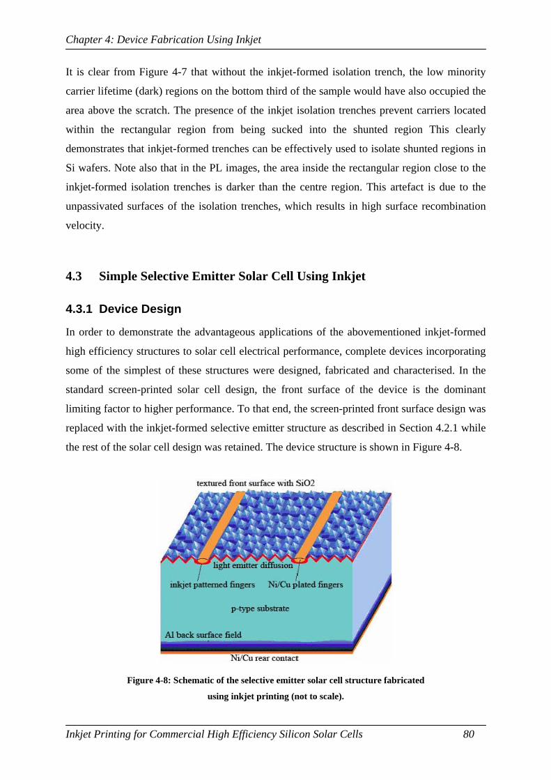
Chapter 4: Device Fabrication Using Inkjet
Inkjet Printing for Commercial High Efficiency Silicon Solar Cells 80
It is clear from Figure 4-7 that without the inkjet-formed isolation trench, the low minority
carrier lifetime (dark) regions on the bottom third of the sample would have also occupied the
area above the scratch. The presence of the inkjet isolation trenches prevent carriers located
within the rectangular region from being sucked into the shunted region This clearly
demonstrates that inkjet-formed trenches can be effectively used to isolate shunted regions in
Si wafers. Note also that in the PL images, the area inside the rectangular region close to the
inkjet-formed isolation trenches is darker than the centre region. This artefact is due to the
unpassivated surfaces of the isolation trenches, which results in high surface recombination
velocity.
4.3 Simple Selective Emitter Solar Cell Using Inkjet
4.3.1 Device Design
In order to demonstrate the advantageous applications of the abovementioned inkjet-formed
high efficiency structures to solar cell electrical performance, complete devices incorporating
some of the simplest of these structures were designed, fabricated and characterised. In the
standard screen-printed solar cell design, the front surface of the device is the dominant
limiting factor to higher performance. To that end, the screen-printed front surface design was
replaced with the inkjet-formed selective emitter structure as described in Section 4.2.1 while
the rest of the solar cell design was retained. The device structure is shown in Figure 4-8.
Figure 4-8: Schematic of the selective emitter solar cell structure fabricated
using inkjet printing (not to scale).

Chapter 4: Device Fabrication Using Inkjet
Inkjet Printing for Commercial High Efficiency Silicon Solar Cells 81
A drawback of the inkjet patterning method is its relatively wider line width compared to
those formed by laser. The front surface contact design must be adapted to this finger width
limitation. To achieve a minimum electrical loss, the optimum balance between the lateral
emitter resistive losses and shading losses due to the metal coverage must be found. The
fractional power loss resulting from the lateral resistance losses is given by (Green 1998):
mp
mpstl V
JSP
×
××=
12
2ρ (4-2)
where Ptl is the fractional power loss due to lateral resistance, sρ is the emitter sheet
resistivity, S is the metal finger spacing, Jmp is the current of the solar cell at maximum power
point and Vmp is the voltage of the solar cell at maximum power point. Additionally, the
fractional power loss due to the finger and busbar shading losses is given by (Green 1998):
S
WP Fsf = (4-3)
B
WP B
sb = (4-4)
where Psf is the fractional power loss due to finger shading, Psb is the fractional power loss
due to busbar shading, WF is the finger width, WB is the busbar width, S is the metal finger
spacing and B is the metal finger length.
Therefore, the total combined fractional power losses due to lateral resistance and shading can
be calculated by adding each loss component as follows:
sbsftltot PPPP ++= (4-5)
In order to calculate the optimum finger spacing S, the following assumptions are used:
• An emitter sheet resistivity sρ of 100 Ω/, thus avoiding any degradation of the
spectral response, particularly in the short wavelength regions.

Chapter 4: Device Fabrication Using Inkjet
Inkjet Printing for Commercial High Efficiency Silicon Solar Cells 82
• Maximum power point current Jmp of 31.5 mA/cm2, which is the typical value for a
selective emitter device as shown in Figure 4-8.
• Maximum power point voltage Vmp of 515 mV, which is the typical value for a
selective emitter device as shown in Figure 4-8.
• Metal finger width WF of 50 µm, which is the typical continuous line width achieved
with indirect inkjet patterning method.
• Busbar width WB of 260 µm and metal finger length B of 26 mm (for a square 8 cm2
area device with front contact pattern as shown in Figure 4-9), which gives a typical
fractional busbar shading loss Psb of 1%.
Figure 4-9: Front contact pattern design for inkjet selective emitter solar cell.
Using Equations (4-2), (4-3), (4-4) and (4-5) and solving S to achieve a minimum value of
Ptot, it was found that the optimum finger spacing is 1.7 mm. This finger spacing results in
1.47% lateral resistance loss, 2.94% finger shading loss and 1% busbar shading loss, thus
giving a total fractional power loss of 5.41%. This is about 1.63% higher power loss
compared to a laser-formed fingers, which has an assumed width of about 25 µm.
Other than the metal covered areas, the rest of the front surface is passivated by thermally
grown SiO2. Due to the presence of the heavily doped contact regions, the emitter diffusion is
less critical compared to the screen-printed design. Therefore, the main consideration for the
emitter design is that it is light enough to achieve good spectral response for the short
wavelength photons without excessive lateral resistance loss. The rest of the device design
follows the structure similar to screen-printed solar cell, including rear Al BSF and the use of
standard p-type, 1 Ω.cm, Czochralski Si wafer with thickness of about 250 µm.
26 mm
1.7 mm
26 mm

Chapter 4: Device Fabrication Using Inkjet
Inkjet Printing for Commercial High Efficiency Silicon Solar Cells 83
4.3.2 Device Fabrication
An outline of the fabrication sequence of the inkjet selective emitter solar cell structure as
shown in Figure 4-8 is presented in Table 4-3. The process sequence is essentially the same as
the standard single-sided buried contact solar cell routinely fabricated at UNSW. The only 3
differences are: (1) the use of inkjet patterning instead of laser in forming the front contact
fingers, (2) the absence of alkaline etch after patterning as there is no Si damage to be
removed, and (3) a shorter Cu plating time because of the wider inkjet-formed finger width.
Steps Parameters
1. Wafer selection p-type boron-doped, 1 Ω.cm, CZ, 300 µm, as-lapped
2. Texturing Alkaline-textured (NaOH/IPA solution)
3. Phosphorus diffusion Solid source deposition at 850 oC for 16 mins – aim 100 Ω/
4. Thermal oxidation
800-1030 oC ramp up, 1030 oC/30 mins TCA oxidation, 980 oC/75 mins wet oxidation, 1030 oC TCA oxidation, 1000 oC
/15mins anneal, ramp down to 800 oC – final sheet resistance
of 100 Ω/
5. Spin coating
Microposit FSC-M Surface Coating (Rohm & Haas), spin
speed of 5,500 rpm/30 secs, followed by oven bake at 140 oC/10 mins – coat both sides
6. Inkjet patterning Front contact fingers 1.7 mm spacing, DEG 1 pL drops, 2
layers, platen at 60 oC
7. Pattern etching BOE (7:1) 8 mins, followed by H2SO4:H2O2 (3:1) 5 mins to
remove surface coating
8. Front contact diffusion Solid source diffusion at 940 oC for 45 mins – aim 5 Ω/
9. Rear contact formation Thermal evaporation of Al (2 µm), alloy at 980 oC/15 hrs
10. Deglazing BOE (15:1) 40 secs
11. Ni plating Ni electroless plating 80-85 oC/5 mins, sinter at 350 oC/10
mins (N2 ambient), 2nd Ni electroless plating 80-85 oC/1 min
12. Cu plating Cu electroless plating 42 oC/3 hrs
13. Edge isolation Laser scribe from rear and cleave
Table 4-3: Fabrication sequence of inkjet selective emitter solar cell.

Chapter 4: Device Fabrication Using Inkjet
Inkjet Printing for Commercial High Efficiency Silicon Solar Cells 84
While the majority of the processing sequences are relatively standard, several problems were
encountered during the processing of inkjet selective emitter solar cells, particularly in the
metallisation step due to the use of inkjet patterning. Figure 4-10 depicts some of the
metallisation problems observed during the development of the device.
Figure 4-10: Optical microscope image of discontinuous metal finger (figure A),
overplated surface (figure B) and excellent plated metal finger (figure C).
Figure 4-10(a) shows an optical microscope image of a discontinuous inkjet patterned finger
line where the plated metal failed to connect. This could result in high series resistance in the
final device due to poor conductivity along the metal fingers. In some cases where the inkjet
patterned lines are not completely continuous, the plated metal would still be able to bridge
the gap because the metal growth is usually isotropic. However, the thickness of the plated
metal is usually only around 15-20 µm, which means that any gaps greater than this would
result in discontinuous metal finger. In order to alleviate this problem, the drop spacing of the
inkjet printed droplets was slightly reduced to 35 µm. This reduction slightly sacrificed
feature size for greater line formation reliability.
Figure 4-10(b) shows an optical microscope image of oxide-protected Si surface overplated
by Cu during the plating process. It was found that the overplating occurred due to the
inability of the spin-coated resin layer to completely protect the peak of the surface pyramids
during the inkjet patterning process. Originally, the typical resulting pyramid heights from the
surface texturing were about 3-5 µm whereas the thickness of the resin as a result of the spin-
coating parameter used was only around 2.5 µm. To avoid overplating, the texturing solution
was modified in order to produce smaller pyramids of about 1-2 µm heights. With these slight
modifications, excellent plated metal fingers could be formed as shown in Figure 4-10(c).
A B C
100μm 100μm 100μm

Chapter 4: Device Fabrication Using Inkjet
Inkjet Printing for Commercial High Efficiency Silicon Solar Cells 85
4.3.3 Device Characterisation
Figure 4-11 shows the current-voltage electrical characteristics of the best-performing initial
device fabricated according to the inkjet selective emitter solar cell structure. The light J-V
curve shown in Figure 4-11(a) was measured against a calibrated reference under STC
condition at 1-sun illumination. The dark J-V curve shown in Figure 4-11(b) was measured
without illumination (in the dark). Additionally, Figure 4-11(b) also plots the calculated local
ideality factor as a function of voltage, which was derived from the differential of the dark J-V
curve. The average electrical performance parameter of a batch of ten solar cells that was
fabricated according to the process sequence of Table 4-3 is also shown.
Figure 4-11: Best electrical performance of an initial inkjet selective emitter
solar cell device showing the measured current-voltage curves against a
calibrated reference under STC conditions at 1-sun illumination (figure A) and
in the dark (filled squares, figure B), together with the calculated local ideality
factor curve as a function of voltage (open squares, figure B). The table shows
the average electrical results of a batch consisting of ten fabricated solar cells.
One of the main highlights of the result shown above is the achievement of an average fill
factor of 80%, which indicates that the inkjet-formed contacts displays excellent contact
formation quality which minimises parasitic losses, particularly due to possible shunts. Due to
its similarity with photolithographically-formed contacts and the absence of structural damage
A B
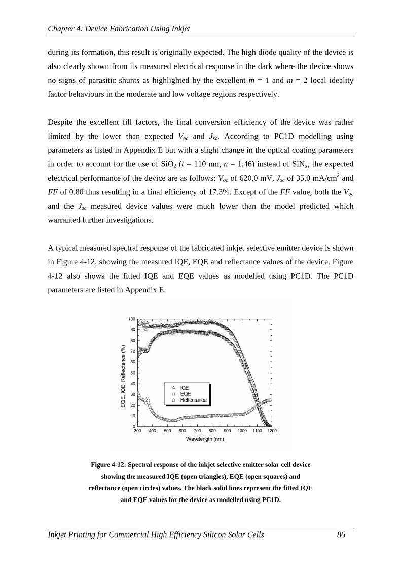
Chapter 4: Device Fabrication Using Inkjet
Inkjet Printing for Commercial High Efficiency Silicon Solar Cells 86
during its formation, this result is originally expected. The high diode quality of the device is
also clearly shown from its measured electrical response in the dark where the device shows
no signs of parasitic shunts as highlighted by the excellent m = 1 and m = 2 local ideality
factor behaviours in the moderate and low voltage regions respectively.
Despite the excellent fill factors, the final conversion efficiency of the device was rather
limited by the lower than expected Voc and Jsc. According to PC1D modelling using
parameters as listed in Appendix E but with a slight change in the optical coating parameters
in order to account for the use of SiO2 (t = 110 nm, n = 1.46) instead of SiNx, the expected
electrical performance of the device are as follows: Voc of 620.0 mV, Jsc of 35.0 mA/cm2 and
FF of 0.80 thus resulting in a final efficiency of 17.3%. Except of the FF value, both the Voc
and the Jsc measured device values were much lower than the model predicted which
warranted further investigations.
A typical measured spectral response of the fabricated inkjet selective emitter device is shown
in Figure 4-12, showing the measured IQE, EQE and reflectance values of the device. Figure
4-12 also shows the fitted IQE and EQE values as modelled using PC1D. The PC1D
parameters are listed in Appendix E.
Figure 4-12: Spectral response of the inkjet selective emitter solar cell device
showing the measured IQE (open triangles), EQE (open squares) and
reflectance (open circles) values. The black solid lines represent the fitted IQE
and EQE values for the device as modelled using PC1D.

Chapter 4: Device Fabrication Using Inkjet
Inkjet Printing for Commercial High Efficiency Silicon Solar Cells 87
The measured spectral response revealed IQE of slightly less than unity in the short
wavelength range between 300-600 nm. This indicates an increased recombination rate on the
top surface of the device. Two likely causes of the observed increased recombination rate are
heavier emitter diffusion and poor passivation on the top surface. Further investigation of the
emitter diffusion process for the device showed that the sheet resistivity of the emitter turned
out to be around 60-65 Ω/, which is heavier than the desired 100 Ω/. This was simply due
to the non-optimised process parameters used in the fabrication process. The front surface
SRV value was also varied to fit the measured IQE better, which resulted in a slightly
increased fitted SRV value of 2500 cm/s.
The major performance degradation however, was likely due to a significant drop in bulk
lifetime during the metallisation process. After the front contact diffusion process (step 8 in
Table 4-3), the average implied Voc was around 660 mV. After the metallisation process, the
average final Voc was only around 605 mV, which indicates a significant 55 mV drop. The
voltage drop is unlikely to be caused by a junction recombination mechanism mainly because
of the device’s high measured fill factor value and the absence of any non-ideal local ideality
factor behaviour in the measured dark J-V curve as shown in Figure 4-11(b).
The most likely process in the metallisation sequence that could cause such a dramatic
reduction in bulk lifetime is the long high temperature Al sintering (980 oC for 15 hours). The
lifetime degradation was probably caused by the presence of damaging contaminants within
the furnace tube during processing due to the equipment’s poor condition. When such
contaminants are diffused into the Si bulk, it usually increases the Shockley-Read-Hall
recombination in the semiconductor material. Other processes in the metallisation sequence
only involve relatively low temperatures, which are unlikely to significantly degrade the bulk
lifetime of the material. The value extracted from the IQE modelling in PC1D indicated a
post-processing bulk lifetime of only around 5 μs.
Regardless of the equipment and process shortcomings, the ability of inkjet-patterned contact
openings to reach very high fill factors strongly indicates the applicability of the inkjet
patterning method towards higher efficiencies in solar cell fabrication. With further
optimisations, it is highly likely that conversion efficiencies above 18% can be reached by
inkjet-processed selective emitter solar cell devices.

Chapter 4: Device Fabrication Using Inkjet
Inkjet Printing for Commercial High Efficiency Silicon Solar Cells 88
4.4 Summary
In this chapter, a range of high efficiency solar cell structures have been fabricated using
indirect inkjet printing method. These structures have previously been demonstrated by using
traditional patterning methods (such as photolithography) to produce significant increases in
solar cell device efficiency. One of the most important high efficiency structures is the
selective emitter structure. The best implementation of selective emitter structure is through
photolithographic patterning. More recently laser patterning has been used to produce similar
structures. This chapter proposed inkjet printing as an alternative patterning method. The
many advantages of using inkjet printing have been discussed. One of the major
disadvantages however, is the comparatively larger feature sizes produced by inkjet
patterning.
While selective emitter structures are usually implemented on the front surface of the solar
cell, major performance improvements can be achieved through the use of localised
contacting scheme through passivating dielectric layer at the rear of the solar cell. A
combination of these types of structures has resulted in the world-record efficiencies
demonstrated by the PERL solar cell. A range of localised contacting schemes that can be
produced using inkjet printing have been discussed. A particularly innovative way of
implementing localised contacts and floating junction passivation using inkjet patterning has
also been proposed. Such structure was previously demonstrated to produce very good
passivation quality on the rear surface of the solar cell.
Other inkjet-formed solar cell structures have also been demonstrated, including: (1) surface
texturing through the formation of inverted pyramids on the front surface of the device,
similar to the light-trapping scheme used by the world-record holding PERL cell, and (2) an
alternative edge isolation technique through a combination of inkjet patterning of dielectric
layer and chemical etching.
Finally, a complete working device that utilises the inkjet-patterned selective emitter structure
was designed and fabricated to provide an example of the use of inkjet printing as a
processing technique in solar cell fabrication. Fill factors as high as 0.800 have been routinely
achieved in these devices, with efficiencies above 18% feasible with further process
optimisations.

Chapter 5: Inkjet Printing of Liquid Dopant Source
Inkjet Printing for Commercial High Efficiency Silicon Solar Cells 89
Chapter 5 : Inkjet Printing of Liquid Dopant Source
5.1 Introduction
One of the most attractive features of inkjet printing is the ability to selectively deposit
materials on the substrate without the use of any mask. In semiconductor fabrication, this is
commonly termed additive processing as opposed to the traditional subtractive method
employed in photolithography. In this case, the fluid used is usually functional, meaning that
the fluid carries an active payload that will eventually stay on the substrate and become part
of the final device.
This chapter presents the evaluation of the viability of using inkjet-printable liquid dopant as a
method of localised doping as well as potentially simultaneous dielectric patterning on Si
wafer substrates. For this initial work, the focus was on using phosphorus-containing liquid
sources that are specially formulated for inkjet printing. Several innovative ways of direct
patterning Si and dielectric layers through the use of inkjet-printed liquid phosphorus sources
will be described, followed by discussions on the fluid formulation and characterisation. Due
to the hydrophilic nature of many dielectric surfaces, appropriate surface treatments are
required. By combining these developments, the direct inkjet patterning method was used to
fabricate a solar cell device in order to demonstrate the applicability of the technique.
5.2 Direct Inkjet Patterning Concepts
5.2.1 Localised Doping on Silicon Surfaces
For standard p-type screen-printed solar cells, the two most common ways of performing
diffusion is by furnace diffusion using either solid, liquid or gaseous sources and by room-
temperature deposition of phosphorus-containing source, such as H3PO4, followed with belt
furnace diffusion. Typically, the H3PO4 is delivered using spray deposition equipment.
Theoretically, inkjet printing can also be used to deposit H3PO4 or other liquid phosphorus
sources onto the entire Si wafer surface. However, it is easy to see that the inkjet printing
deposition method would be disadvantageous compared to the spray deposition method,
mainly due to its much slower speed.

Chapter 5: Inkjet Printing of Liquid Dopant Source
Inkjet Printing for Commercial High Efficiency Silicon Solar Cells 90
A more suitable application of liquid dopant sources by inkjet printing is to perform localised
deposition of dopant sources on a Si wafer substrate, followed by subsequent high
temperature treatment in a furnace. This approach fully utilises the strengths of the inkjet
deposition method. Selective inkjet deposition of liquid dopant sources with appropriate
polarities would allow the maskless direct patterning of multiple distinct diffusion regions on
Si surfaces. The significant reduction in process steps by using inkjet patterning instead of
photolithography is depicted in the process flowchart comparison shown in Figure 5-1.
Figure 5-1: Process steps flowchart comparison between localised diffusion
using traditional photolithography and inkjet printing of liquid dopant.
The illustration in Figure 5-1 shows that the number of processing steps can be potentially
reduced from seven to just two steps by using inkjet liquid dopant deposition to achieve local
diffusion on Si wafer surfaces. In addition, there are significant cost savings such as:
• Materials savings with the inkjet method (only liquid dopant required) compared to
costly photoresist and developer solution and others such as acid dielectric etchants
needed for photolithography.
• Less material wastage in the inkjet method as the liquid dopant is only deposited
where needed. This is in contrast to the use of photoresist, which is completely
removed afterwards.
• Only one high temperature step (furnace drive-in) is required with the inkjet method
compared to two steps (oxide growth and furnace diffusion) in photolithography.
Oxide growth
Photo-resist
UV expose & develop
Oxide removal
Photoresist removal
Furnace diffusion
Inkjet print
Oxide removal
Furnace drive-in

Chapter 5: Inkjet Printing of Liquid Dopant Source
Inkjet Printing for Commercial High Efficiency Silicon Solar Cells 91
The application of inkjet liquid dopant as shown in Figure 5-1 does not retain any dielectric
layer at the end of the localised diffusion process. While this structure might not be suitable
for solar cell structures that require pre-patterned dielectric layers, there are some other
structures where this inkjet patterning method could be useful. An example of a solar cell
design that would benefit from this particular application of inkjet printed liquid dopant is the
semiconductor finger solar cell structure (Wenham et al. 2005).
The semiconductor finger technology implements a selective emitter structure while still
employing screen-printed metallisation. This is achieved through the formation of closely-
spaced, thin and heavily doped transparent “fingers” on a lightly doped front surface. The
metal fingers are then screen-printed perpendicular to these transparent fingers such that metal
contacts are made only where the two fingers intersect. The transparent fingers help transfer
collected carriers to the metal fingers. This allows the metal fingers to be spaced further apart
resulting in reduced shading without increasing the lateral emitter resistive losses.
Instead of the traditional method of using a laser to form shallow grooves followed by furnace
heavy diffusion to form the semiconductor fingers, liquid dopant sources could be inkjet
printed on bare textured Si surfaces to define the heavily-doped semiconductor fingers on the
wafer. The following lists a possible process sequence for fabricating a semiconductor finger
solar cell structure using inkjet printing of liquid dopant sources on standard commercial CZ
wafers:
1. Surface texturing using alkaline etching.
2. Inkjet printing of liquid dopant sources to define semiconductor fingers on the front
surface, followed by suitable drying of the printed dopant sources.
3. High temperature drive-in of printed dopant sources, combined with light emitter
diffusion on the front surface.
4. Diffusion glass removal.
5. Edge junction isolation.
6. PECVD SiNx deposition on the front surface.
7. Screen printing of rear and front metal pastes.
8. Metal co-firing.

Chapter 5: Inkjet Printing of Liquid Dopant Source
Inkjet Printing for Commercial High Efficiency Silicon Solar Cells 92
Besides forming localised doped surfaces on bare Si surfaces, inkjet printing can also be used
as a precision method of depositing liquid dopants on pre-fabricated localised openings such
as holes or grooves. A comparison between the traditional method of achieving such localised
diffusion using furnace diffusion and the alternative approach using inkjet deposition of liquid
dopant followed by high temperature drive-in step is shown in Figure 5-2. In both cases, the
dielectric opening is assumed to be fabricated beforehand using an arbitrary method.
Figure 5-2: Process steps flowchart comparison between diffusion through
localised dielectric opening using conventional furnace diffusion and inkjet
printing of liquid dopant.
One of the advantages of locally inkjet depositing the liquid dopant sources instead of the
conventional homogenous furnace diffusion process is the ability to constrain dopant
diffusion only to areas where the dopant sources are present. This is particularly beneficial
when diffusion of dopants are undesirable in other parts of the Si wafer, for instance on the
rear, sides or other regions on the front surface.
Localised deposition of dopant sources using inkjet is also advantageous when used to
fabricate solar cell structures where two different diffusion polarities are required either on
single or both surfaces of the Si wafer. An example of such structure is the interdigitated
contacting scheme whereby an inkjet device can be used to deposit both p-type and n-type
dopant sources, followed by only a single high temperature step to drive both dopants sources
into the Si.
Oxide growth
Dielectric patterning
Furnace diffusion
+
Furnace drive-in
Inkjet print

Chapter 5: Inkjet Printing of Liquid Dopant Source
Inkjet Printing for Commercial High Efficiency Silicon Solar Cells 93
5.2.2 Simultaneous Patterning and Doping on Dielectric Surfaces
In some solar cell structures, it is still preferable to be able to pattern dielectric layers and
perform localised diffusion on the subsequently exposed Si surfaces. Generally, at least two
processing steps are required to achieve this: one process for patterning and another for
diffusion. The concept of inkjet liquid dopant deposition as presented in Section 5.2.1 is only
targeted towards the direct patterning of Si surfaces, but not dielectric surfaces. It is desirable
to develop a method of combining both dielectric patterning and Si diffusion.
A novel concept for using inkjet-printed liquid dopant sources as a dielectric patterning tool
as well as a selective diffusion method is presented in Figure 5-3. Note that in this particular
technique, phosphorus is the only preferred liquid dopant source due to its known ability to
alter the etching rate of certain dielectric materials.
Figure 5-3: Process steps flowchart of simultaneous dielectric patterning and
selective diffusion through inkjet printing of liquid dopant source.
This patterning method relies on the presence of etching selectivity between intrinsic and
phosphorus-doped dielectric layer. The starting surface maybe a dielectric layer commonly
used in solar cell fabrication such as SiO2 or SiNx. Inkjet printing is then used to deposit
liquid phosphorus sources on top of the dielectric surface, followed by high temperature
drive-in of the printed phosphorus droplets. The drive-in step must allow the phosphorus
source to diffuse through the entire thickness of the dielectric layer, and preferably also
diffuse the underlying Si surface to create selective doping in these regions. The wafer may
then be immersed in dielectric etchant solution, such as dilute HF, which etches the
phosphorus-diffused regions of the dielectric significantly faster than the unaffected regions.
The etching selectivity generally depends on the amount of phosphorus doping present within
the dielectric layer thickness with higher concentration resulting in faster etching.
Apply dielectric
Inkjet print
High temp drive-in
Wet etch

Chapter 5: Inkjet Printing of Liquid Dopant Source
Inkjet Printing for Commercial High Efficiency Silicon Solar Cells 94
As mentioned before, the high temperature drive-in step not only results in changing the
etching selectivity of the dielectric layer but also has the potential to diffuse the Si layer
underneath to create a localised doped Si region. Using this method, only one high
temperature step is required to form both the dielectric opening and the heavy diffusion. The
final concentration of phosphorus dopant in the Si depends on the amount of dopant atoms
available at the dielectric-silicon interface. Obviously, the thicker the dielectric layer, the
more difficult it is for the dopant atoms to reach the dielectric-silicon interface.
The above-mentioned inkjet patterning method can be immediately applied to simple
selective emitter structures whereby metals are directly deposited onto the heavily diffused Si
regions that are exposed. An example of a suitable self-aligning metallisation method to
achieve this purpose is through chemical plating where the metal preferably deposits onto the
Si. In this case, the rest of the unpatterned surfaces are protected from any metal deposition by
the retained dielectric layer. The deposited metal then makes intimate contact onto the heavily
doped Si surface, which result in a good ohmic contact.
A possible process sequence for fabricating a selective emitter solar cell structure using the
inkjet printing of liquid dopant sources method as described above is as follows:
1. Surface texturing using alkaline etching.
2. Light emitter diffusion on the front surface.
3. Diffusion glass removal.
4. Edge junction isolation.
5. PECVD SiNx deposition on the front surface.
6. Inkjet printing of liquid dopant sources on the SiNx surface.
7. Furnace drive-in of printed liquid dopant sources.
8. Selective wet chemical etching to form openings on the patterned SiNx layer
9. Screen printing of rear Al metal, followed by firing.
10. Ni/Cu/Ag chemical plating.
Two extra equipments that are needed are an inkjet device and a chemical plating system. The
relative suitability of this type of concept to existing production lines makes it an attractive
proposition for retrofitting in pursuit of higher efficiency device structures.

Chapter 5: Inkjet Printing of Liquid Dopant Source
Inkjet Printing for Commercial High Efficiency Silicon Solar Cells 95
5.3 Jettable Liquid Dopant Sources and Surface Treatment
In order to conduct a preliminary proof-of-concept work for these innovative approaches of
using inkjet printed liquid dopant sources in solar cell fabrication, it is necessary to first
develop an appropriate inkjet process for this application. The approach taken for such
development is essentially similar to the one described at length in Section 2.3. Once again,
the central role of inkjet process development is the fluid formulation which determines the
viability of the printhead used to eject it. Another particularly important consideration in this
development process is the specific treatments that may need to be applied to the surfaces as
both surfaces used in this work (Si and dielectric surfaces) exhibit markedly different
behaviours when in contact with the inkjet printed liquid.
For convenience, boron and phosphorus are the designated dopants of choice in this work for
the p-type and n-type dopants respectively due to their widespread use in solar cell
applications. It is important to mention that for the localised doping on Si concept discussed
in Section 5.2.1, both boron and phosphorus dopant sources can be used. On the other hand,
for the dielectric patterning concept described in Section 5.2.2, only phosphorus dopant
sources are suitable for this method due to the observed increase in etching rate of
phosphorus-doped dielectric layers. As a result, the preliminary development work presented
in this section focuses only on liquid phosphorus dopant sources. Nevertheless, it is noted that
mostly similar limitations, requirements and performance are similarly applicable to liquid
boron dopant sources.
5.3.1 Phosphoric Acid-based Liquid Dopant Sources
The most obvious choice of phosphorus-containing liquid that is readily available as a source
for inkjet-printable dopant diffusion is phosphoric acid (H3PO4). It is a low-cost solution that
is produced commercially at a significant quantity and is widely used in semiconductor
process, particularly as the preferred etchant of SiNx layers. The solution is acidic (pH ~1.5),
so corrosion in the printhead material requires particular attention.
In order to investigate the compatibility between H3PO4 and the materials used in the
printhead construction, a compatibility test was conducted by immersing the material
compatibility kit (MCK) provided by the printhead manufacturer in the solution to be jetted.

Chapter 5: Inkjet Printing of Liquid Dopant Source
Inkjet Printing for Commercial High Efficiency Silicon Solar Cells 96
The highest possible liquid concentration of H3PO4 is 85%, above which the solution becomes
solid. Therefore, the tests were conducted at room temperature using this concentration. In
this trial, only the Dimatix DMC-11601 printhead was investigated for compatibility due to its
suitability for preliminary work. A list containing the DMC-11601 printhead components is
presented in Appendix C.
After seven consecutive days of immersion in H3PO4 (85%) solution, these five components
were removed from the solution, rinsed under deionised (DI) water and then dried using N2
gun. Preliminary visual checks by naked eye showed no observable physical changes to the
materials. Closer examination through the use of an optical microscope on the surfaces of the
components further confirmed the positive results.
Table 5-1 lists the fluid properties of H3PO4 (85%) that are relevant to jetting quality. The
right column shows the optimum jetting parameters of the DMC-11601 printhead.
H3PO4 (85%) Optimum jetting
Molecular weight 98.00 N/A
Particle content size (μm) none < 1.00
Viscosity @ 25 oC (cP) 47.00 8.00 – 14.00
Surface tension @ 25 oC (mN/m) 80.70 28.00 – 36.00
Density (g/cm3) 1.69 > 1.00
Boiling point (oC) 158.00 > 100.00
Table 5-1: Fluid properties as relevant to jetting for H3PO4 (85%).
Both the viscosity and surface tension of H3PO4 (85%) are too high for optimum jetting. To
rectify these parameters, the most straight-forward way is to heat up the fluid. To reduce the
viscosity of H3PO4 (85%) to the upper range of the optimum viscosity value (14.0 cP), the
fluid needs to be heated up to around 60 oC, which gives a viscosity of around 13.4 cP.
However, in the case of H3PO4 (85%), fluid heating is undesirable due to: (1) possible
compatibility issues due to increased reactivity between the fluid and the printhead, and (2)
operational safety reasons of using acidic solutions at elevated temperature.

Chapter 5: Inkjet Printing of Liquid Dopant Source
Inkjet Printing for Commercial High Efficiency Silicon Solar Cells 97
An alternative way of modifying the viscosity and surface tension of a fluid is by diluting the
solution. In the case of H3PO4, the solvent used is H2O, which has viscosity and surface
tension values of 0.89 cP and 71.97 mN/m (at 25 oC) respectively. The low viscosity of H2O
should dramatically reduce the viscosity to within the optimum value. However, the high
surface tension of H2O limits the achievable minimum diluted surface tension to ~72 mN/m.
Both the change of viscosity and surface tension, as well as density of the diluted H3PO4 as a
function of various concentrations is shown in Figure 5-4. The H3PO4 was diluted by adding
H2O to the 85% concentrated solution. The viscosity values were measured using Brookfield
DV-II+ Pro viscometer (Brookfield Engineering). The surface tension values were measured
using an Analite STM2141 surface tension meter (McVan Instruments). Both measurements
of viscosity and surface tension were performed at a fluid temperature of about 25 oC. The
density values were obtained from Corbridge (2000).
Figure 5-4: Viscosity (open squares), surface tension (open circles), and density
(open triangles) of diluted H3PO4 solution as a function of its concentration.
The closest optimal viscosity was obtained at about 50% H3PO4 concentration. The measured
surface tension and density at this concentration were 75.73 mN/m and 1.33 g/cm3
respectively. Despite the high surface tension value of the H3PO4 solution, it was found that
the fluid was still jettable with good jetting quality as long as the jetting parameters
(particularly the jetting waveform) are appropriately optimised.

Chapter 5: Inkjet Printing of Liquid Dopant Source
Inkjet Printing for Commercial High Efficiency Silicon Solar Cells 98
Approximately 1.5 mL of H3PO4 (50%) solution was loaded into a 1 pL DMC-11601
printhead using a syringe injection through a 0.2 μm pore size filter. The printhead was left
idle for at least 24 hours with the nozzles facing down to allow the fluid to fill the pumping
chambers inside the printhead and to ensure that the fluid is properly degassed. Afterwards,
the printhead was installed onto the DMP system and then primed for use. The fluid was
maintained at room temperature during jetting. The jetting quality was characterised visually
through the drop watcher system by adjusting the jetting voltage and waveform.
The best jetting parameters were found to be a jetting voltage of 16 V, jetting pulse length of
8.768 μs and jetting frequency of 5 kHz. The jetting performance quickly deteriorates as the
jetting frequency is increased, particularly due to the high surface tension of the fluid which
inhibits priming of the jets at the beginning of each jetting cycle. Figure 5-5 shows the jetting
waveform used to jet the H3PO4 (50%) solution using the DMP device.
Figure 5-5: Jetting waveform used to jet H3PO4 (50%) in the DMP.
There are two additional considerations with regard to the H3PO4 (50%)-based inkjet-
printable liquid dopant sources described above. The first one is related to the use of a lower
concentration of H3PO4 solution. It is obvious that to achieve the heaviest diffusion possible,
higher concentration of phosphorus source is preferable. Nevertheless, calculations of the
available amount of phosphorus atoms in a 1 pL droplet of H3PO4 (50%) reveals that the
concentration is in the order of 1021 atoms/cm3, which is higher than the solid solubility value
of phosphorus in Si at 800-1000 oC temperature range.

Chapter 5: Inkjet Printing of Liquid Dopant Source
Inkjet Printing for Commercial High Efficiency Silicon Solar Cells 99
The second consideration relates to the beneficial effect of the high surface tension value of
the H3PO4 (50%) solution in this direct inkjet patterning application. Unlike the indirect inkjet
patterning method, in which the droplet almost immediately diffuses into the “absorbent”
resin layer, the deposited droplets of dopant sources remain as liquid on the Si or dielectric
surfaces. To achieve the finest feature sizes on the surface, higher fluid surface tension is
preferable to prevent spreading of the deposited droplet. The surface energy of the substrate
also plays an equally important role in determining the degree of spreading. This aspect of the
deposition method will be discussed in more details in Section 5.3.3.
5.3.2 Specially-formulated Liquid Dopant Sources
One of the key advantages of specially-formulated solutions is the greater control on the
overall composition of the fluid, which optimises the fluid properties to obtain desirable
results such as fine feature size and heavy diffusion. Another advantage is the ability to
synthesise safer formulations that are preferably less acidic and corrosive, which is beneficial
both from printhead compatibility and operational safety points of view.
At the beginning of this thesis work, there were no known commercially-available products
for inkjet-printable liquid dopant sources. The closest available product for this purpose was
liquid spin-on-dopants (SOD). Most of the trialled SOD products were difficult to jet due to
their lower-than-optimal viscosities. The most serious drawback, however, was the low
boiling point of the solution due to the use of alcohols as the main solvent. It was found that
consistent jetting was virtually impossible to achieve as the rate of solvent evaporation (at
room temperature) far exceeded the jetting frequency, thus resulting in depletion of solutions
in liquid phase at the nozzle orifice. Over time, this evaporation effect left an accumulation of
dried residues, particularly around the orifice perimeter which further inhibited good jetting.
In order to create a suitable inkjet-printable liquid phosphorus dopant source, Honeywell
Electronic Materials (HEM) was engaged in a collaborative development. Honeywell was
responsible for the chemical formulation of the liquid phosphorus dopant source, while the
author’s work was mainly focused on the testing, characterisation and application of the
resulting product. A general approach used in the formulation process is presented in
Appendix F.
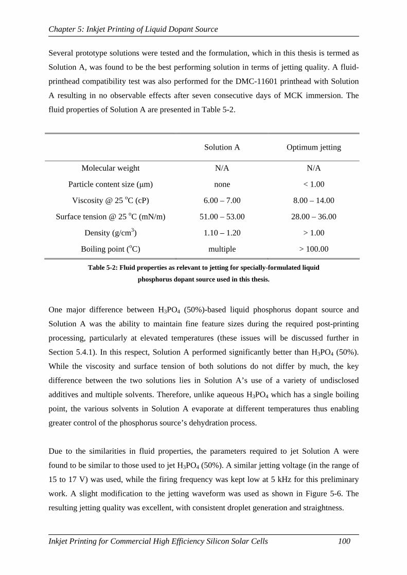
Chapter 5: Inkjet Printing of Liquid Dopant Source
Inkjet Printing for Commercial High Efficiency Silicon Solar Cells 100
Several prototype solutions were tested and the formulation, which in this thesis is termed as
Solution A, was found to be the best performing solution in terms of jetting quality. A fluid-
printhead compatibility test was also performed for the DMC-11601 printhead with Solution
A resulting in no observable effects after seven consecutive days of MCK immersion. The
fluid properties of Solution A are presented in Table 5-2.
Solution A Optimum jetting
Molecular weight N/A N/A
Particle content size (μm) none < 1.00
Viscosity @ 25 oC (cP) 6.00 – 7.00 8.00 – 14.00
Surface tension @ 25 oC (mN/m) 51.00 – 53.00 28.00 – 36.00
Density (g/cm3) 1.10 – 1.20 > 1.00
Boiling point (oC) multiple > 100.00
Table 5-2: Fluid properties as relevant to jetting for specially-formulated liquid
phosphorus dopant source used in this thesis.
One major difference between H3PO4 (50%)-based liquid phosphorus dopant source and
Solution A was the ability to maintain fine feature sizes during the required post-printing
processing, particularly at elevated temperatures (these issues will be discussed further in
Section 5.4.1). In this respect, Solution A performed significantly better than H3PO4 (50%).
While the viscosity and surface tension of both solutions do not differ by much, the key
difference between the two solutions lies in Solution A’s use of a variety of undisclosed
additives and multiple solvents. Therefore, unlike aqueous H3PO4 which has a single boiling
point, the various solvents in Solution A evaporate at different temperatures thus enabling
greater control of the phosphorus source’s dehydration process.
Due to the similarities in fluid properties, the parameters required to jet Solution A were
found to be similar to those used to jet H3PO4 (50%). A similar jetting voltage (in the range of
15 to 17 V) was used, while the firing frequency was kept low at 5 kHz for this preliminary
work. A slight modification to the jetting waveform was used as shown in Figure 5-6. The
resulting jetting quality was excellent, with consistent droplet generation and straightness.

Chapter 5: Inkjet Printing of Liquid Dopant Source
Inkjet Printing for Commercial High Efficiency Silicon Solar Cells 101
Figure 5-6: Jetting waveform used to jet Solution A in the DMP.
The slightly less acidic nature of Solution A compared to H3PO4 (50%) did not result in
significant printhead lifetime extension. The printhead lifetime was characterised by the
ability of at least one nozzle to jet the fluid with the same jetting quality as when the fluid was
first loaded into the printhead. For the DMC-11601 printhead, it was observed that the jetting
quality deteriorated after a period of about 3-4 weeks. The most common failure mode was
found to be either non-jetting or poor droplet flight trajectory. A likely cause of both problems
is the accumulation of dried fluid residues around the perimeter of the nozzle orifice. This
build-up of residue obstructs the fluid flow as it is pushed out of the nozzle. In the worst case
scenario, the accumulated residue completely blocked the nozzle and prevented any fluid
jetting.
The attempt to formulate a less acidic fluid resulted in a solution that contained a lower
concentration of phosphorus. In the case of Solution A, the actual phosphorus concentration
after dissolution in the solvent is only 5-7% (w/v), while the phosphorus solid content ranges
from around 30-40% (w/v). Assuming that the density of Solution A is around 1.1-1.2 g/cm3
as given in Table 5-2, a 1 pL droplet still contains a phosphorus atom concentration in the
order of 1021 atoms/cm3, which is a figure that is at least similar or higher to the solid
solubility of phosphorus in Si in the process temperature range between 800-1000 oC.

Chapter 5: Inkjet Printing of Liquid Dopant Source
Inkjet Printing for Commercial High Efficiency Silicon Solar Cells 102
5.3.3 Surface Preparations and Characterisation
Two types of surfaces are considered in the development of direct inkjet patterning concepts
through the printing of liquid dopant sources. The bare, HF-treated Si surface used in the first
application as described in Section 5.2.1 is a hydrophobic surface, while the dielectric surface
(primarily SiNx and SiO2) used in the second application as described in Section 5.2.2 is a
hydrophilic surface. Obviously, in order to achieve the finest feature sizes possible, a
hydrophobic surface is desirable as the spherical droplet shape is retained when the droplet
contacts the surface, thus creating a small contact area between the surface and droplet.
As discussed in Section 2.3.3, the solid surface energy determines the wetting behaviour of a
particular surface. Contact angle measurements using a goniometer can be used to
characterise the surface energy of a solid surface. To better predict the wettability of a surface,
the critical surface tension of a solid surface can be measured and calculated. This parameter
represents the minimum surface tension threshold of a liquid, below which complete wetting
will occur.
Gould and Irene (1988) found that the critical surface tension of an HF-treated Si surface was
~27 mN/m. This means that any liquid with a surface tension above 27 mN/m will not wet the
surface. Both the H3PO4 (50%) and Solution A used in this work have very high surface
tension values of 80.7 mN/m and 51.0 mN/m respectively. It is important to note that this low
critical surface tension value only applies for HF-treated Si surface as Si by itself has been
identified by Jaccodine (1963) as a very high energy solid with measured surface free energy
value of 2130 mN/m for (100) surfaces. This highlights the importance of having hydrogen
and fluorine species passivating the Si surface in order to achieve the low surface energy
value.
In order to measure the resulting contact angle, goniometer measurements were performed on
pipette-formed droplets of H3PO4 (50%) and Solution A onto three different Si surface
finishes: random upright pyramid textured, saw-damage-etched and mirror-polished surfaces.
The Si wafer surfaces were not diffused. Any surface oxide was removed from these surfaces
by immersion in BHF (7:1) solution before any measurements were made. The measurements
were taken at room temperature using a Rame-Hart Model 200-F1 goniometer. Table 5-3 lists
the contact angle measurement results for the two fluids.

Chapter 5: Inkjet Printing of Liquid Dopant Source
Inkjet Printing for Commercial High Efficiency Silicon Solar Cells 103
HF-treated Si surface H3PO4 (50%) Solution A
Random pyramid textured 104.6 62.8
Saw damage etched 58.9 43.2
Mirror-polished 74.8 63.2
Table 5-3: Measured contact angles (in degrees) of pipette-dropped H3PO4
(50%) and Solution A on three different HF-treated Si surface finishes.
Droplets of H3PO4 (50%) form higher contact angles compared to Solution A due to their
higher surface tension value. With contact angles higher than 90o for textured surfaces, these
droplets of H3PO4 (50%) results in very narrow printed lines on the HF-treated Si surface. The
higher contact angle exhibited by the textured surface can be attributed to the rougher surface
structure due to the presence of the microscopic pyramids. Although rough surface usually
makes it difficult for the fluid droplet to pin down a contact line that minimises its energy, the
dimension of the pyramids (~1 µm) in this case is at least an order of magnitude smaller
compared to the droplet diameter (~15-20 µm). As a result, the roughness is hardly ‘visible’
to the droplet and may minimise spreading by allowing the droplet to quickly define its
contact line along the valleys of the pyramids.
Surface roughness becomes less advantageous when the surface structure is comparable to the
size of the droplet. This situation is clearly demonstrated by the lowest contact angle shown
by the saw-damage-etched surface. In this case, the droplet attempts to minimise its energy by
spreading along the surface until it meets a trough on the rough surface. The flat case is
shown by the mirror-polished surface which shows a marked improvement in its measured
contact angle compared to the saw-damage-etched surface.
The formation of narrow inkjet-printed lines is more complicated when dielectric surfaces
such as SiO2 or SiNx are considered. Williams and Goodman (1974) have investigated the
wetting behaviour of H2O on SiO2 surfaces with varying oxide thickness and found that these
surfaces are completely hydrophilic (i.e. contact angle of almost 0o) for oxide thicknesses
greater than 30 Å. Goniometer contact angle measurements performed on both SiO2 and SiNx
surfaces using pipette-dropped H3PO4 (50%) and Solution A further verified the complete-
wetting behaviour of dielectric surfaces, thus implying high surface energies.

Chapter 5: Inkjet Printing of Liquid Dopant Source
Inkjet Printing for Commercial High Efficiency Silicon Solar Cells 104
A common way to modify surface properties is through surface functionalisation. Specific
functional groups can be added onto the surface through a number of methods. Plasma
processing is one surface functionalisation method that is regularly used to introduce certain
atoms or molecules onto a surface. Another popular method is through immersion or spin-
coating of specific solutions that attach layers of functional groups onto a surface.
The functionalisation of SiO2 surfaces to achieve hydrophobicity has been previously
demonstrated. For instance, Lim et al. (2005) showed that the application of hexamethyl-
disilazane (HMDS) or octadecyltrichlorosilane (OTS) onto SiO2 surfaces by spin-coating or
immersion resulted in an increase of the measured contact angle of H2O droplets with values
of 53.76o and 78.98o respectively.
Similarly for SiNx, functionalisation of the surface through the use of attached organic
monolayers by reacting SiNx-coated Si wafer surfaces with solutions of 1-alkenes and 1-
alkynes have been demonstrated by Arafat et al. (2007) to produce high measured contact
angles in excess of 100o. Despite this, SiNx is known to be a difficult surface to functionalise
due to its intrinsic electronegative nitrogen groups on the surface. This makes it easier for
hydrogen atoms in a polar molecule to interact in a strong dipole-dipole interaction in the
form of hydrogen bonding.
One important issue that needs to be considered when functionalising surfaces is the fact that
the inkjet-deposited liquid phosphorus dopant source must be able to penetrate these layers to
act on the underlying SiNx layer. Another consideration is when the deposited fluid has
penetrated the functionalised layer and then comes into contact with the underlying SiNx
(which is hydrophilic). Since the fluid is not reactive to the SiNx underneath but reactive to
the adjacent functionalised layers, the fluid droplet is likely to have a tendency to spread
laterally along the surface.
In this work, an alternative and simple method of creating hydrophobic SiO2 and SiNx
surfaces was used. The method involved heating the SiO2 or SiNx-coated Si wafers in a
conventional fan-forced oven at 250 oC in ambient air for at least 1 hour. This heat treatment
appears to change the surface from being hydrophilic to hydrophobic as indicated in the
goniometer images shown in Figure 5-7. The fluid used was H3PO4 (50%) deposited by a
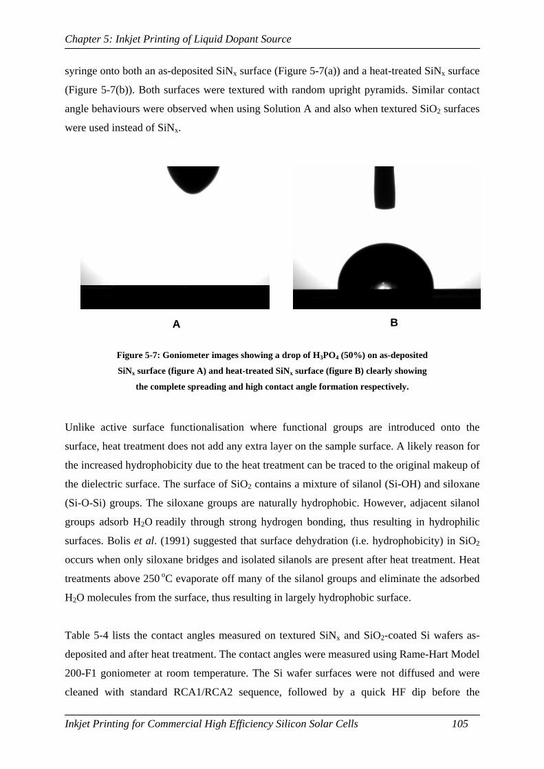
Chapter 5: Inkjet Printing of Liquid Dopant Source
Inkjet Printing for Commercial High Efficiency Silicon Solar Cells 105
syringe onto both an as-deposited SiNx surface (Figure 5-7(a)) and a heat-treated SiNx surface
(Figure 5-7(b)). Both surfaces were textured with random upright pyramids. Similar contact
angle behaviours were observed when using Solution A and also when textured SiO2 surfaces
were used instead of SiNx.
Figure 5-7: Goniometer images showing a drop of H3PO4 (50%) on as-deposited
SiNx surface (figure A) and heat-treated SiNx surface (figure B) clearly showing
the complete spreading and high contact angle formation respectively.
Unlike active surface functionalisation where functional groups are introduced onto the
surface, heat treatment does not add any extra layer on the sample surface. A likely reason for
the increased hydrophobicity due to the heat treatment can be traced to the original makeup of
the dielectric surface. The surface of SiO2 contains a mixture of silanol (Si-OH) and siloxane
(Si-O-Si) groups. The siloxane groups are naturally hydrophobic. However, adjacent silanol
groups adsorb H2O readily through strong hydrogen bonding, thus resulting in hydrophilic
surfaces. Bolis et al. (1991) suggested that surface dehydration (i.e. hydrophobicity) in SiO2
occurs when only siloxane bridges and isolated silanols are present after heat treatment. Heat
treatments above 250 oC evaporate off many of the silanol groups and eliminate the adsorbed
H2O molecules from the surface, thus resulting in largely hydrophobic surface.
Table 5-4 lists the contact angles measured on textured SiNx and SiO2-coated Si wafers as-
deposited and after heat treatment. The contact angles were measured using Rame-Hart Model
200-F1 goniometer at room temperature. The Si wafer surfaces were not diffused and were
cleaned with standard RCA1/RCA2 sequence, followed by a quick HF dip before the
A B
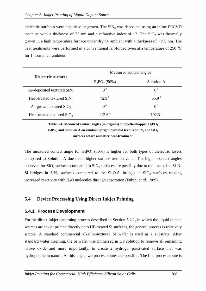
Chapter 5: Inkjet Printing of Liquid Dopant Source
Inkjet Printing for Commercial High Efficiency Silicon Solar Cells 106
dielectric surfaces were deposited or grown. The SiNx was deposited using an inline PECVD
machine with a thickness of 75 nm and a refractive index of ~2. The SiO2 was thermally
grown in a high temperature furnace under dry O2 ambient with a thickness of ~350 nm. The
heat treatments were performed in a conventional fan-forced oven at a temperature of 250 oC
for 1 hour in air ambient.
Measured contact angles Dielectric surfaces
H3PO4 (50%) Solution A
As-deposited textured SiNx 0 o 0 o
Heat-treated textured SiNx 72.9 o 65.9 o
As-grown textured SiO2 0 o 0 o
Heat-treated textured SiO2 112.6 o 102.3 o
Table 5-4: Measured contact angles (in degrees) of pipette-dropped H3PO4
(50%) and Solution A on random upright pyramid textured SiNx and SiO2
surfaces before and after heat-treatment.
The measured contact angle for H3PO4 (50%) is higher for both types of dielectric layers
compared to Solution A due to its higher surface tension value. The higher contact angles
observed for SiO2 surfaces compared to SiNx surfaces are possibly due to the less stable Si-N-
Si bridges in SiNx surfaces compared to the Si-O-Si bridges in SiO2 surfaces causing
increased reactivity with H2O molecules through adsorption (Fubini et al. 1989).
5.4 Device Processing Using Direct Inkjet Printing
5.4.1 Process Development
For the direct inkjet patterning process described in Section 5.2.1, in which the liquid dopant
sources are inkjet printed directly onto HF-treated Si surfaces, the general process is relatively
simple. A standard commercial alkaline-textured Si wafer is used as a substrate. After
standard wafer cleaning, the Si wafer was immersed in HF solution to remove all remaining
native oxide and more importantly, to create a hydrogen-passivated surface that was
hydrophobic in nature. At this stage, two process routes are possible. The first process route is

Chapter 5: Inkjet Printing of Liquid Dopant Source
Inkjet Printing for Commercial High Efficiency Silicon Solar Cells 107
where the liquid dopant sources are inkjet-printed directly onto the un-diffused Si surface.
The second process route is where a standard impurity diffusion process (phosphorus is used
in the case of p-type substrate) is performed on the surface, followed by diffusion glass
removal and then inkjet printing of liquid dopant sources. The general process flowchart for
the direct inkjet patterning of phosphorus liquid dopant sources on Si surface is shown in
Figure 5-8.
Figure 5-8: Process flowchart of direct inkjet patterning of phosphorus liquid
dopant sources on Si surface.
Further investigations of both the diffused and un-diffused surfaces of Si revealed significant
differences in the wetting behaviour of inkjet-printed liquid dopant sources. Both the HF-
treated un-diffused and diffused Si surfaces were found to have a very high degree of
hydrophobicity immediately after the HF-treatment as evidenced by the high contact angle
measurements obtained using both types of phosphorus liquid dopant sources. However, it
was observed that the diffused Si surface lost its hydrophobicity considerably quicker than the
un-diffused Si surface. This phenomenon can be attributed to the fact that native oxide grows
much faster in n+ (100) Si surfaces than in n (100) Si surfaces at room temperature in air
ambient as has been previously shown by Morita et al. (1990).
The inkjet printing step selectively deposited the liquid phosphorus dopant sources on the
surface of the solar cell. The substrate was heated to ~60 oC during printing in order to
enhance the evaporation of some of the solvent from the deposited liquid dopant source upon
contact with the substrate surface. Using the 1 pL DMC-11601 printhead to inkjet-print both
the H3PO4 (50%) and Solution A onto textured diffused and un-diffused Si surfaces, line
widths of 15-20 µm were routinely achieved as shown in Figure 5-9(a) and Figure 5-9(b).
Optimisation of droplet spacing had to be performed to achieve the most continuous line
possible during printing. If the drop spacing was too small, bulges along the printed line
Diffused surface
Un-diffused surface
HF treatment
Inkjet printing Drying High temp
drive-in
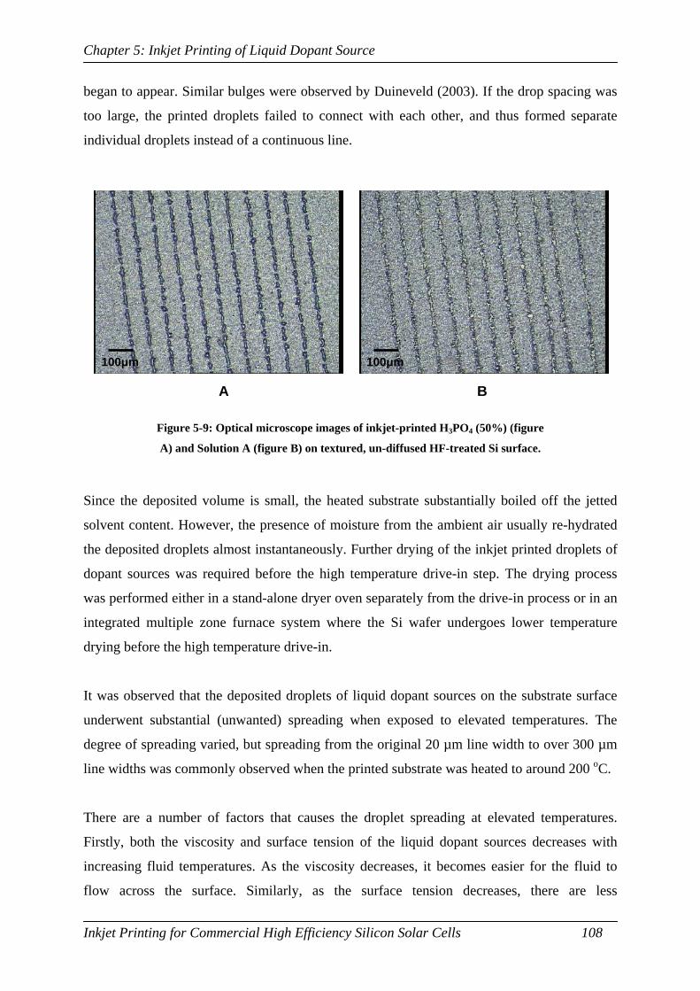
Chapter 5: Inkjet Printing of Liquid Dopant Source
Inkjet Printing for Commercial High Efficiency Silicon Solar Cells 108
began to appear. Similar bulges were observed by Duineveld (2003). If the drop spacing was
too large, the printed droplets failed to connect with each other, and thus formed separate
individual droplets instead of a continuous line.
Figure 5-9: Optical microscope images of inkjet-printed H3PO4 (50%) (figure
A) and Solution A (figure B) on textured, un-diffused HF-treated Si surface.
Since the deposited volume is small, the heated substrate substantially boiled off the jetted
solvent content. However, the presence of moisture from the ambient air usually re-hydrated
the deposited droplets almost instantaneously. Further drying of the inkjet printed droplets of
dopant sources was required before the high temperature drive-in step. The drying process
was performed either in a stand-alone dryer oven separately from the drive-in process or in an
integrated multiple zone furnace system where the Si wafer undergoes lower temperature
drying before the high temperature drive-in.
It was observed that the deposited droplets of liquid dopant sources on the substrate surface
underwent substantial (unwanted) spreading when exposed to elevated temperatures. The
degree of spreading varied, but spreading from the original 20 µm line width to over 300 µm
line widths was commonly observed when the printed substrate was heated to around 200 oC.
There are a number of factors that causes the droplet spreading at elevated temperatures.
Firstly, both the viscosity and surface tension of the liquid dopant sources decreases with
increasing fluid temperatures. As the viscosity decreases, it becomes easier for the fluid to
flow across the surface. Similarly, as the surface tension decreases, there are less
A B
100μm
100μm

Chapter 5: Inkjet Printing of Liquid Dopant Source
Inkjet Printing for Commercial High Efficiency Silicon Solar Cells 109
intermolecular forces within the liquid molecules to hold it together and it is eventually
overcome by the fluid-solid molecular forces with the substrate surface. The spreading
tendency is further exacerbated by the formation of native oxide as the temperature is raised
in air ambient. The presence of native oxide considerably increases the surface energy of the
substrate, which causes complete wetting on the surface.
Essentially, the drying step is a dehydration process. For instance, in the case of H3PO4
(50%), the drying process converts liquid H3PO4 into solid phosphorus pentoxide (P2O5).
Similarly, for Solution A, the acid-based liquid compound is also converted into P2O5 through
dehydration. Water is the main solvent in the case of H3PO4, which has a boiling point of 100 oC. H3PO4 itself has a boiling point of 158 oC. Above this temperature, polyphosphoric acid is
formed. Further removal of water results in a range of dehydrated forms of H3PO4, consisting
of pyrophosphoric acid (H4P2O7) and metaphosphoric acid (HPO3). When the acid is fully
dehydrated, the resulting compound is solid P2O5. This solid compound itself sublimes at
temperatures above 300 oC (Corbridge 2000).
In order to achieve dehydration at elevated temperatures without droplet spreading, a special
vacuum drying method was developed. The technique involved establishing a vacuum
environment before the temperature was raised for drying. The low pressure environment is
believed to remove much of the moisture out of the ambient air, which prevents native oxide
growth on the surface. Once the drying process was completed, it was presumed that only
solid P2O5 remained on the surface. Although P2O5 is a strong dessicant, it was observed that
after vacuum dehydration, further high furnace temperature treatment in atmospheric
conditions did not cause any spreading.
The vacuum drying technique is equally applicable to both HF-treated Si surfaces and heat-
treated dielectric surfaces such as SiO2 and SiNx. The visual appearance before and after the
vacuum drying did not appear to change significantly except that the wet liquid look of the
inkjet-printed lines before drying turned into a more glassy solid look after drying. This is
illustrated in the optical microscope images shown in Figure 5-10, which shows the
appearance of inkjet-printed Solution A lines on heat-treated textured SiNx surface before and
after the vacuum drying.

Chapter 5: Inkjet Printing of Liquid Dopant Source
Inkjet Printing for Commercial High Efficiency Silicon Solar Cells 110
Figure 5-10: Optical microscope images of Solution A inkjet-printed on heat-
treated SiNx surface before (figure A) and after (figure B) vacuum drying.
After the inkjet-printed phosphorus dopant sources were dried, high temperature treatment
was used to drive the phosphorus atoms into the substrate. The process is essentially a
standard solid state diffusion process that is commonly used in semiconductor fabrication and
has been reviewed extensively on many textbooks such as by Sze (2002).
One major difference is the limited amount of phosphorus atoms available from inkjet-printed
droplets of liquid dopant sources. Due to the sublimation of P2O5 at temperatures above 300 oC and the absence of continuous source of phosphorus dopants in the ambient, it is inevitable
that the diffusion process is severely limited by the availability of the printed dopants.
Evidently, it is much more difficult to diffuse impurities onto a narrow 20 µm line from a
similarly-sized dopant source compared to diffusion on entire surface such as those performed
on an inline diffusion system with H3PO4 as sprayed precursor liquid. Furthermore, there are
no accurate measurement technique to determine the actual doping concentration and profile
of an active area as small as those produced by this inkjet printing technique (~15-20 µm).
To characterise the diffusion that was achieved using inkjet printing of liquid phosphorus
dopant sources, four-point-probe measurements were used to measure the sheet resistivity of
the diffused layer. However, it is difficult to use a four-point-probe to measure resistivities for
narrow regions such as those produced by inkjet printing. Therefore, a solid large area pad
(~10 mm 10 mm) was inkjet-printed on the surface to enable probing using the available
four-point-probe instrument. Obviously, the measurements made using this technique are not
A B
100μm
100μm

Chapter 5: Inkjet Printing of Liquid Dopant Source
Inkjet Printing for Commercial High Efficiency Silicon Solar Cells 111
an accurate representation of the actual doping that occurs from the 20 µm printed lines.
However, measurements from the large area pads were useful for initial investigations into
whether the liquid dopant sources, were able to diffuse into the substrate surface.
The actual diffusion of inkjet-printed phosphorus liquid dopant sources was estimated by
extrapolating measured sheet resistivities resulting from printed pads of decreasing size.
Three types of surfaces on Si substrates were considered: (1) HF-treated diffused textured Si
wafer, (2) heat-treated diffused textured Si wafer with SiNx, and (3) heat-treated diffused
textured Si wafer with SiO2.
Inkjet printing of Solution A was done on each surface in the shape of individual solid pads of
varying area with a layout as shown in Figure 5-11. During the inkjet printing step, the
substrate was heated to 60 oC. Afterwards, the wafers were all vacuum-dried in a vacuum
chamber at 200 oC, followed by belt furnace drive-in at 980 oC for 3 hours in air ambient. The
sheet resistivity of each of the pads was then measured using a four-point-probe.
Figure 5-11: Layout of inkjet-printed pads of varying sizes.
Due to the small area of the measurement pads, the four-point-probe measurements had to be
adjusted by an area-related correction factor. A method to calculate the appropriate correction
factor was given by Smits (1958) and is presented in Appendix G.
The resulting sheet resistivities are presented in Figure 5-12 as a function of the various pad
widths for all three different surfaces (Si surface, SiNx surface and SiO2 surface).
15x10mm
15x8mm
15x6mm
15x4mm
15x2mm
Pad areas:
• 15 x 10mm • 15 x 8mm • 15 x 6mm • 15 x 4mm • 15 x 2mm • 15 x 1mm • 15 x 0.5mm

Chapter 5: Inkjet Printing of Liquid Dopant Source
Inkjet Printing for Commercial High Efficiency Silicon Solar Cells 112
Figure 5-12: Measured sheet resistivities of diffused inkjet-printed pads as a
function of pad area for Si surface (filled circles), SiNx surface (filled squares)
and SiO2 surface (filled triangles). Trend lines are added as guides to the eye.
The measurement result on the largest-size pad on Si surface indicates that Solution A was
able to diffuse the Si very heavily, in the region of ~3 Ω/. This heavy diffusion confirms that
the formulation does not fundamentally limit the diffusion capability of printable dopant
sources. The diffusions performed through dielectric coatings resulted in much higher sheet
resistivities due to the presence of dielectric barrier. Nevertheless, the reasonably heavy
diffusions of around 25-30 Ω/ is sufficient for contacting purposes.

Chapter 5: Inkjet Printing of Liquid Dopant Source
Inkjet Printing for Commercial High Efficiency Silicon Solar Cells 113
With decreasing pad sizes, the sheet resistivities appear to decrease. This trend is particularly
evident in the results obtained for diffusions involving Si surfaces where the phosphorus
dopants are able to directly diffuse into the Si. The trend is less clear on the dielectric
surfaces, presumably due to the presence of the dielectric barriers, which makes the diffusion
less uniform due to various non-uniformities on the dielectric layer such as thickness or
hardness (density). This result must be viewed with caution because even the smallest
measurable pad width is 1 mm wide or 50 times wider than the width of the inkjet-printed
liquid phosphorus dopant source line. At such a microscopic scale, various effects such as
vapour mass transfer or P2O5 sublimation may become very influential and might drastically
change the amount of phosphorus atoms available for the diffusion.
The concern regarding insufficient phosphorus on single pass, single line printing of a liquid
phosphorus dopant source was confirmed when a test structure was fabricated as follows. A
batch of Si wafers was coated with PECVD SiNx on one surface with the standard 75 nm
thickness and refractive index of ~2. The wafers were then heat-treated to create hydrophobic
SiNx surface and then inkjet printed with a series of parallel lines of Solution A spaced 1 mm
apart. Only a single pass for each line was printed. The wafers were vacuum-dried and the
resulting line width was ~20-25 µm. The wafers then underwent high temperature drive-in in
a belt furnace at a temperature of 980 oC for a total of 3 hours in air ambient. The wafers were
then immersed in HF (1:10) solution for a total of 30 minutes with regular visual and optical
microscope checks every 5 minutes to see whether or not selective etching has occurred.
Selective etching was observed for the first 5 minutes and then appeared to have stopped
thereafter. This result suggests that some penetration through the SiNx did occur, but not for
the entire thickness of the dielectric layer. Some of the possible implications are: (1)
insufficient available dopant source after drying, or (2) significant loss of dopant sources
during the high temperature treatment, or (3) a longer drive-in time was required. The process
temperature for drying is less than the sublimation temperature of P2O5 (>300 oC) and thus
unlikely to cause significant loss of phosphorus atoms. However, it is quite likely that the
high drive-in temperature could cause either sublimation of P2O5 or vapour mass transfer of
phosphorus atoms from the inkjet-printed region to the ambient. The third hypothesis was
found to be unlikely as longer high temperature treatments as long as a total of 6 hours at 980 oC did not show any improvement in the etching selectivity of the SiNx layer.

Chapter 5: Inkjet Printing of Liquid Dopant Source
Inkjet Printing for Commercial High Efficiency Silicon Solar Cells 114
To alleviate this problem, multiple pass printing was trialled instead of single pass printing.
This resulted in wider lines, although presumably also resulted in an increased phosphorus
source volume on the surface. Using similar SiNx-coated wafers as substrate and the standard
direct inkjet patterning process, successively higher number of passes were printed onto a test
wafer. It was found that the printing of just two adjacent lines was sufficient to produce the
desired etching selectivity of the SiNx. Double line printing means that two connected parallel
lines were printed instead of one single line, thus doubling the line width from 20-25 µm to
40-50 µm. This method enabled the direct inkjet patterning of the SiNx layer.
5.4.2 Device Concept and Fabrication
A simple selective emitter solar cell structure similar to the one used to demonstrate the
applicability of the indirect inkjet patterning method in Chapter 3 was also used to
demonstrate the usefulness of the direct inkjet patterning method. A schematic of the device
structure was shown in Figure 4-8.
Instead of using indirect inkjet patterning method to form the front metal grid patterning, the
direct inkjet patterning of SiNx layer and simultaneous diffusion underneath the metal contact
regions were used to create the front metal contacts. If SiO2 was used as opposed to SiNx, the
method would have been similarly applicable. Also, in this case, Solution A was used as the
liquid phosphorus dopant source, although H3PO4 (50%) could also have been used.
An outline of the fabrication sequence for this direct-inkjet-patterned selective emitter solar
cell structure is presented in Table 5-5. The main differences between this fabrication
sequence and the one for indirect inkjet patterning are: (1) SiNx is used as a dielectric layer
following the industry standard, (2) the use of direct inkjet patterning instead of indirect inkjet
patterning, (3) no second heavy diffusion was required due to the intended simultaneous
heavy diffusion achieved during the direct inkjet patterning process. The rest of the
processing sequence remains the same.

Chapter 5: Inkjet Printing of Liquid Dopant Source
Inkjet Printing for Commercial High Efficiency Silicon Solar Cells 115
Steps Parameters
1. Wafer selection p-type boron-doped, 1 Ω.cm, CZ, 300 µm, as-lapped
2. Texturing Alkaline-textured (NaOH/IPA solution)
3. Phosphorus diffusion Solid source deposition at 850 oC for 40 mins – aim 100 Ω/
4. Diffusion glass removal HF (1:10) etch
5. PECVD SiNx deposition Remote-PECVD, thickness: 75 nm, refractive index: ~2
6. Heat treatment Conventional fan-forced oven, 250 oC for 1 hour, air ambient
7. Inkjet patterning Front contact fingers 1.7 mm spacing, Solution A 1 pL drops,
50 µm wide (2 parallel connected passes), platen at 60 oC
8. Vacuum drying Pressure ~0.1-0.3 mbar, temperature: 200-300 oC, time: ~10-
15 minutes
9. Drive-in Belt furnace, 980 oC for a total of 3 hours
10. Etching HF(1:10) for 3-5 mins
11. Rear contact formation Thermal evaporation of Al (2 µm), alloy at 980 oC/15 hrs
12. Deglazing HF (10:1) 50 secs
13. Ni plating Ni electroless plating 80-85 oC/5 mins, sinter at 350 oC/5 mins
(N2 ambient), 2nd Ni electroless plating 80-85 oC/1 min
14. Cu plating Cu electroless plating 42 oC/3 hrs
15. Edge isolation Laser scribe from rear and cleave
Table 5-5: Fabrication sequence of direct-inkjet-patterned selective emitter
solar cell.
5.4.3 Device Characterisation
Figure 5-13 shows the current-voltage electrical characteristics of the best-performing initial
device fabricated according to the inkjet selective emitter solar cell structure. The light J-V
curve shown in Figure 5-13(a) was measured against a calibrated reference under STC
condition at 1-sun illumination. The dark J-V curve shown in Figure 5-13(b) was measured
without illumination (in the dark). Additionally, Figure 5-13(b) also plots the calculated local
ideality factor as a function of voltage, which was derived from the differential of the dark J-V
curve.

Chapter 5: Inkjet Printing of Liquid Dopant Source
Inkjet Printing for Commercial High Efficiency Silicon Solar Cells 116
Figure 5-13: Best electrical performance of an initial direct-inkjet-patterned
selective emitter solar cell device showing the measured current-voltage curves
against a calibrated reference under STC conditions at 1-sun illumination
(figure A) and in the dark (filled squares, figure B), together with the calculated
local ideality factor curve as a function of voltage (open squares, figure B).
Although the device fabricated here is only a test structure with no optimisation, some
explanations on the poor electrical parameters are useful to determine the factors that could
improve the device performance in subsequent work. There are several possible reasons for
the measured low Jsc value. The non-optimised front surface design in this device causes
higher-than-usual shading losses. This is further exacerbated by the presence of overplated
copper on the front surface due to inability of SiNx coating to fully mask the peaks of the
pyramids from the plating process.
The low Voc value can be attributed to several reasons. Firstly, the poor quality of the heavily
contaminated belt furnace at UNSW that was used for the high-temperature drive-in severely
degraded the bulk lifetime of the device. The same belt furnace was also used by Edwards
(2008) to fire screen-printed dopant pastes at high temperature with similar degradation in
bulk lifetime. The second effect that reduces the Voc can probably be attributed to high
junction recombination, particularly in the contact regions of the device. The impact of this
recombination loss will be explored further in the discussion on fill factor losses.
A B

Chapter 5: Inkjet Printing of Liquid Dopant Source
Inkjet Printing for Commercial High Efficiency Silicon Solar Cells 117
The fill factor loss is the main investigation point in this case, especially in evaluating the
impact of direct inkjet patterning as a method of forming metal contacts on solar cell devices.
The dark J-V measurement result shown in Figure 5-13(b) clearly indicates that the m > 1
recombination dominates in this device in the medium to high voltage range. This
characteristic ‘hump’ implies that there is likely to be a detrimental shunt recombination
effect that limits the fill factor of the device (McIntosh 2001). Subsequent Suns-Voc
measurement of this sample gave a pseudo fill factor (pFF) of 0.601. The fact that the
measured pFF value is not much higher than the measured FF of 0.590 under illumination
provides further evidence that the dominant loss is due to a parasitic shunt effect rather than a
series resistance effect.
A likely cause for the observed shunt is the non-uniformity of the phosphorus diffusion in the
direct-inkjet-patterned regions such that there is a mixture of p-type and n-type regions
contacting the deposited metal. When these localised p-type regions make a contact with the
metal, they create localised Schottky barriers and also localised shunts with the adjacent n-
type regions, thus contributing to the m > 1 recombination as observed in the dark J-V curve.
This theory was verified by introducing additional dopants through the following method.
Another batch of samples was fabricated following the same procedure as described in Table
5-5. An additional inkjet deposition of liquid phosphorus dopant source was dispensed only
into the exposed Si after the etching step (Step 10), followed by an extra high temperature
drive-in step in the same belt furnace at 980 oC for 1 hour. The purpose of this extra selective
diffusion step is to ensure that enough phosphorus was diffused into the Si underneath the
metal contacts. A comparison of the measured light J-V electrical parameters of the devices
with and without additional phosphorus diffusion is shown in Table 5-6.
Voc (mV) Jsc (mA/cm2) FF η
No additional diffusion 498.0 27.50 0.590 8.11
With additional diffusion 549.1 27.96 0.736 11.30
Table 5-6: Comparison of electrical parameters of direct-inkjet-patterned
selective emitter solar cell with and without additional phosphorus diffusion
measured against a calibrated reference under STC condition at 1-sun
illumination.

Chapter 5: Inkjet Printing of Liquid Dopant Source
Inkjet Printing for Commercial High Efficiency Silicon Solar Cells 118
There is a significant improvement in the measured fill factor after the extra diffusion process
on the patterned contact regions from 0.590 to 0.736. This result provides further evidence to
the hypothesis of there being insufficient phosphorus atoms diffused in the Si because it
clearly shows that additional phosphorus diffusion eliminates the localised Schottky barriers
caused by localised metal-p-type region contacts. The Voc is also noticeably increased by
about 50 mV due to the elimination of these parasitic ‘high junction recombination’ regions.
Suns-Voc measurement was performed on the sample with additional phosphorus diffusion
showing a high pFF of 0.794, thus indicating that most of the fill factor losses can now be
attributed to the parasitic series resistance losses due to the non-optimised emitter design.
Finally, a comparison between the m-V curve of the samples before and after extra
phosphorus diffusion as shown in Figure 5-14 clearly shows the elimination of the increased
local ideality factor previously observed in the medium to high voltage range.
Figure 5-14: Comparison of m-V curve between samples before (filled squares)
and after (open squares) extra phosphorus diffusion.
The results presented above indicate that although direct inkjet patterning of SiNx using the
concept discussed in Section 5.2.2 proves to be challenging, it still appears to be possible to
achieve high fill factor contact formation using the method. The problems concerning the
poor electrical performance of the initial fabricated device have been identified, thus making
improvements possible and demonstrating that there is a feasible application of the newly
developed direct inkjet patterning concept to solar cell fabrication.

Chapter 5: Inkjet Printing of Liquid Dopant Source
Inkjet Printing for Commercial High Efficiency Silicon Solar Cells 119
5.5 Summary
In this chapter, two new concepts of directly patterning Si and dielectric surfaces by utilising
inkjet-printable liquid dopant sources have been proposed. The first concept simply involves
the direct deposition of liquid dopant sources onto bare Si surfaces to form selectively
diffused regions. The second concept involves the direct deposition of phosphorus liquid
dopant sources onto dielectric surfaces such as SiO2 or SiNx, whereby the phosphorus dopants
are used to diffuse through both the dielectric layer and the underlying Si. The diffused
phosphorus modifies the etchability of the dielectric layer creating high etching selectivity,
which can be advantageously-used for dielectric patterning purposes. Simultaneously, the
phosphorus dopants also diffuse into the underlying Si, thus creating a highly-doped region
where the metal contact will eventually be deposited.
Two types of liquid phosphorus dopant source formulations were described and their potential
to act as printable dopants compared. The first type of solution was based on off-the-shelf
standard highly concentrated phosphoric acid. The second solution was jointly developed with
an external chemical manufacturer with the aim of reducing the acidity of the original
phosphoric acid-based solution as well as improving the fine line width capability and
jettability of the solution. Various fluid properties, printhead compatibility and jetting
optimisation were performed and discussed in order to illustrate the development path of an
inkjet-printable solution as well as the ink-jetting capability of the formulated solutions. To
complete the inkjet system development procedure, the various surface types used in this
work were reviewed. Several issues regarding their hydrophobicity were identified and
solved. A method of creating hydrophobic SiO2 and SiNx surfaces was developed and was
shown to be capable of producing fine lines as narrow as 15-20 µm using inkjet printing of
liquid phosphorus dopant sources.
Finally, the newly developed direct inkjet patterning concept was applied to the fabrication of
a solar cell device. The inkjet process was used to fabricate a simple selective emitter solar
cell structure to demonstrate the feasibility of the patterning technique. The limited amount of
diffused phosphorus that resulted from using the inkjet doping process proved to be the
biggest challenge in achieving high fill factor contact formation in the device. Nevertheless,
the limiting cell performance factors have been identified and discussed, which is useful for
future work.

Chapter 6: Conclusion
Inkjet Printing for Commercial High Efficiency Silicon Solar Cells 120
Chapter 6 : Conclusion
The primary aim of this thesis was to conceptualise, develop and demonstrate the applicability
of using inkjet printing as a viable alternative patterning method. In the past,
photolithography, laser patterning and screen-printing have been the most commonly used
patterning method in solar cell fabrication. As a result, many higher efficiency solar cell
designs have been developed using these tools. However, the drive to reduce fabrication costs
requires an alternative patterning approach that combines low-cost, high-throughput, high-
resolution and contactless characteristics. In this thesis, inkjet printing was proposed as a
possible solution that satisfies all of these requirements.
Although inkjet printing have been previously used as a tool to deposit a number of functional
fluids (such as metal inks) in solar cell fabrication, the use of such method to directly pattern
and form localised openings on dielectric layers have never been explored before. The lack of
systematic way of developing a suitable inkjet system, particularly for solar cell fabrication
purposes, provided the motivation for the synthesis of such method. It was found that the
inkjet system can be broken down to three main components consisting of printhead, fluid and
substrate.
The development of two novel and distinct inkjet patterning methods represents the key
innovation resulting from this thesis work. The first method involved the deposition of
plasticiser droplets onto an intermediate resin layer that coats the dielectric layer on the
substrate surface, thus creating regions that are permeable to aqueous dielectric etchants such
as HF. The underlying dielectric layer can then be selectively etched and patterned. The final
removal of the resin layer exposed the patterned dielectric layer.
The second method involved the direct deposition of functional fluids, specifically in the form
of liquid dopant sources onto both Si and dielectric surfaces. In the case of Si surfaces, the
inkjet-printed liquid dopant sources can be selectively deposited to form localised diffusion
layers. In the case of dielectric surfaces, the inkjet-printed liquid dopant sources can be used
to simultaneously form openings on the dielectric layer and selective diffusion in the
underlying Si surface.

Chapter 6: Conclusion
Inkjet Printing for Commercial High Efficiency Silicon Solar Cells 121
Using the indirect method, individual round openings with diameters as small as 30-35 μm
and continuous line patterns with width as narrow as 40-50 μm could be formed on dielectric
surfaces. Using the direct method, lines as narrow as 15-20 μm were formed on both Si and
dielectric surfaces. Additionally, a vacuum-drying method was developed to prevent droplet
spreading at elevated temperatures and a simple baking method was developed to make
normally-hydrophilic dielectric surfaces become hydrophobic.
As a result of these developments, solar cell devices with fill factors above 0.800 have been
fabricated using the indirect method, thus showing the excellent quality of the patterning
process. Furthermore, working solar cell devices have been fabricated using the direct
method, with the performance-limiting factors identified.
6.1 Original Contributions
The following are the original contributions arising from this thesis work:
• The development of a novel dielectric patterning method by inkjet-depositing droplets
of plasticiser onto a resin layer thus creating a permeable layer that would allow
aqueous etchants to etch the underlying dielectric layer.
• The identification of diethylene glycol and novolac resin as a suitable plasticiser-resin
combination for the above-mentioned dielectric patterning method.
• The demonstration of patterns produced using the above-mentioned dielectric
patterning method producing round openings with diameters as small as 30-35 μm and
continuous line patterns with width as narrow as 40-50 μm.
• The demonstration of various high efficiency solar cell structures, including selective
emitter structure, localised contacting scheme, surface texturing and edge isolation
produced the above-mentioned dielectric patterning method.
• The fabrication of a complete solar cell with front surface contacts patterned using the
above-mentioned dielectric patterning with fill factor as high as 0.80.

Chapter 6: Conclusion
Inkjet Printing for Commercial High Efficiency Silicon Solar Cells 122
• The development of a novel selective diffusion method by inkjet-depositing droplets
of liquid phosphorus dopant sources onto a silicon surface followed by a high
temperature treatment.
• The development of a novel simultaneous dielectric patterning and selective diffusion
method by inkjet-depositing droplets of liquid phosphorus dopant sources onto a
dielectric layer followed by a high temperature treatment and selective chemical
etching of the dielectric layer.
• The demonstration of the use of vacuum drying to produce a narrow line width of ~15-
20 μm of the inkjet-printed liquid phosphorus dopant sources on both silicon and
dielectric surfaces.
• The demonstration of the use of a heat treatment to transform the originally
hydrophilic dielectric surfaces into hydrophobic surfaces.
• The fabrication of a complete solar cell with front surface contacts patterned and
selectively diffused using the simultaneous inkjet-printed patterning/diffusion process
of liquid phosphorus dopant sources with fill factor as high as 0.79.
6.2 Future Work
Due to the novelty of the work, there are numerous opportunities to further develop the inkjet
patterning methods described here. Some suggestions for further works are given below:
1. Indirect inkjet patterning method
• In this work, only the novolac-DEG combination of resin-plasticiser was
evaluated as the initial proof-of-concept. Theoretically, any resin-plasticiser is
a potential candidate to be used in the indirect inkjet patterning method. It is
likely that there are other resin-plasticiser combinations capable of producing
smaller feature sizes than the novolac-DEG combination. It would be useful to
further evaluate a wide range of plasticisers and resin formulations.

Chapter 6: Conclusion
Inkjet Printing for Commercial High Efficiency Silicon Solar Cells 123
• One of the main advantages of using plasticiser instead of solvent in the
indirect inkjet printing method is that plasticiser droplets do not form openings
on the resin layer. The retention of the resin layer offers the possibility of
reversing the permeability of the patterned resin layer. The reversibility would
allow multiple patterning to be performed on the same resin layer, thus
reducing wastage and the number of process steps involved.
2. Direct inkjet patterning method
• One of the major problems encountered in the direct inkjet patterning process
is the tendency for the droplets to form bulges along the printed line, which
results in discontinuous lines. This raises serious difficulties in forming
continuous diffusion regions that are essential to conduct currents generated by
the solar cell. More work is required to further understand the surface
behaviour and to find possible surface treatments that avoid this problem.
• Another major problem was the low level of attainable diffusion of dopants
from the inkjet-deposited liquid. The various physical and chemical events that
occur during the high temperature drive-in process needs to be understood in
order to determine the best way to perform such localised diffusions.
Furthermore, it may be possible to formulate a fluid containing chemical
binder such that loss of phosphorus atoms is minimised during processing.
3. Inkjet-processed high efficiency solar cell devices
• Both the indirect and direct inkjet patterning method described in this thesis
can be used as a patterning tool to create many different solar cell structures
that are capable of achieving higher efficiencies. Some of these concepts have
been proposed and discussed in Chapter 4. The implementation of these
structures onto a real solar cell design and the fabrication of such devices
would be invaluable in evaluating the benefits of using these inkjet patterning
methods on the device’s electrical performance.

Inkjet Printing for Commercial High Efficiency Silicon Solar Cells 124
This page is intentionally left blank.

References
Inkjet Printing for Commercial High Efficiency Silicon Solar Cells 125
References
Abbott M. 2006, “Advanced laser processing and photoluminescence characterisation of high
efficiency silicon solar cells”, PhD Thesis, University of New South Wales, Kensington.
Abbott M. D., Cotter J. E., Trupke T., and Bardos R. A. 2006, “Investigation of edge
recombination effects in silicon solar cell structures using photoluminescence”, Applied
Physics Letters, Vol. 88, No. 11, DOI:10.1063/1.2186510.
Altermatt P. P., Heiser G., Dai X., Jürgens J., Aberle A. G., Robinson S. J., Young T.,
Wenham S. R., and Green M. A. 1996, “Rear surface passivation of high-efficiency silicon
solar cells by a floating junction”, Journal of Applied Physics, Vol. 80, No. 6, pp. 3574-3586.
Arafat A., Giesbers M., Rosso M., Sudhölter E. J. R., Schroën K., White R. G., Yang L.,
Linford M. R., and Zuilhof H. 2007, “Covalent biofunctionalization of silicon nitride
surfaces”, Langmuir, Vol. 23, No. 11, pp. 6233-6244.
Arias A. C., Daniel J., Kursor B., Ready S., Sholin V., and Street R. 2007, “All-additive ink-
jet-printed display backplanes: Materials development and integration”, Journal of the Society
for Information Display, Vol. 15, No. 7, pp. 485-490.
Baekeland L. H. 1909, “Method of making insoluble products of phenol and formaldehyde”,
U.S. Patent 942,699.
Basore P. 2006, “CSG-1: Manufacturing a new polycrystalline silicon PV technology”,
Proceedings of the 4th World Conference on Photovoltaic Energy Conversion (Hawaii), pp.
2089-2093.
Bibl A., Chen Z., and Birkmeyer J. 2005, “Print head with thin membrane”, U.S. Patent
Publication 2005/0099467 A1.

References
Inkjet Printing for Commercial High Efficiency Silicon Solar Cells 126
Bibl A., Higginson J. A., Essen K. V., and Xu A. 2006a, “Single-use droplet ejection
module”, U.S. Patent Publication 2006/0158489 A1.
Bibl A., Higginson J. A, Hoisington P. A., Gardner D. A., Hasenbein R. A., Biggs M. L., and
Moynihan E. R. 2006b, “Printhead having a thin pre-fired piezoelectric layer”, U.S. Patent
7,052,117 B2.
Biehl S., Danzebrink R., Oliveira P., and Aegerter M. A. 1998, “Refractive microlens
fabrication by ink-jet process”, Journal of Sol-Gel Science and Technology, Vol. 13, No. 1-3,
pp. 177-182.
Bietsch A., Zhang J., Hegner M., Lang H. P., and Gerber C. 2004, “Rapid functionalization of
cantilever array sensors by inkjet printing”, Nanotechnology, Vol. 15, pp. 873-880.
Biro D., Erath D., Belledin U., Specht J., Stüwe D., Lemke A., Aleman M., Mingirulli N.,
Rentsch J., Preu R., Schlosser R., Bitnar B., and Neuhaus H. 2007, “Inkjet printing for high
definition industrial masking processes for solar cell production”, Proceedings of 17th
International Photovoltaic Science and Engineering Conference (Fukuoka).
Blakers A. W., Wang A., Milne A. M., Zhao J., and Green M. A. 1989, “22.8% efficient
silicon solar cell”, Applied Physics Letters, Vol. 55, No. 13, pp. 1363-1365.
Bolis V., Fubini B., Marchese L., Martra G., and Costa D. 1991, “Hydrophillic and
hydrophobic sites on dehydrated crystalline and amorphous silicas”, Journal of the Chemical
Society: Faraday Transactions, Vol. 87, No. 3, pp. 497-505.
Bonaccurso E., Butt H., Hankeln B., Niesenhaus B., and Graf K. 2005, “Fabrication of
microvessels and microlenses from polymers by solvent droplets”, Applied Physics Letters,
Vol. 86, No. 12, 124101.
Borojevic N., Ho-Baillie A., Utama R., Lennon A., Lenio M., Karpour A., and Wenham S.
2008, “Inkjet texturing for high efficiency commercial silicon solar cells”, Proceedings of
23rd European Photovoltaic and Solar Energy Conference (Valencia).
References
Inkjet Printing for Commercial High Efficiency Silicon Solar Cells 127
Brünahl J. 2003, “Physics of piezoelectric shear mode inkjet actuators”, PhD Thesis, Royal
Institute of Technology, Stockholm.
Bruton T., Mason N., Roberts S., Hartley O. N., Gledhill S., Fernandez J., Russell R., Warta
W., Glunz S., Schultz O., Hermle M., and Willeke G. 2003, “Towards 20% efficient silicon
solar cells manufactured at 60 MWp per annum”, Proceedings of 3rd World Conference on
Photovoltaic Energy Conversion (Osaka), pp. 899-902.
Campbell P. and Green M. A. 1987, “Light trapping properties of pyramidally textured
surfaces”, Journal Applied Physics, Vol. 62, No. 1, pp. 243-249.
Carter J. C., Alvis R. M., Brown S. B., Langry K. C., Wilson T. S., McBride M. T., Myrick
M. L., Cox W. R., Grove M. E., and Colston B. W. 2005, “Fabricating optical fiber imaging
sensors using inkjet printing technology: A pH sensor proof-of-concept”, Biosensors and
Bioelectronics, Vol. 21, No. 7, pp. 1359-1364.
Chan B. O. 1993, “Defects in silicon solar cell materials”, PhD Thesis, University of New
South Wales, Kensington.
Clugston D. A. and Basore P. A. 1997, “PC1D version 5: 32-bit solar cell modelling on
personal computers”, Proceedings of the 26th IEEE Photovoltaic Specialists Conference
(Anaheim), pp. 207-210.
Cooley P., Wallace D., and Antohe B. 2002, “Applications of ink-jet printing technology to
bioMEMS and microfluidic systems”, Journal of the Association for Laboratory Automation,
Vol. 7, No. 5, pp. 33-39.
Corbridge D. E. C. 2000, Phosphorus 2000: Chemistry, Biochemistry and Technology,
Elsevier Science & Technology.
Cox W. R. and Chen T. 2001, “Micro-optics fabrication by ink-jet printing”, Optics and
Photonics News, Vol. 12, No. 6, pp.32-35.

References
Inkjet Printing for Commercial High Efficiency Silicon Solar Cells 128
De Ceuster D., Cousins P., Rose D., Cudzinovic M., and Mulligan W. 2007, “Low cost, high
volume production of >22% efficiency silicon solar cells” Proceedings of 22nd European
Photovoltaic and Solar Energy Conference (Milan).
Deegan R. D., Bakajin O., Dupont T. F., Huber G., Nagel S. R., and Witten T. A. 1997,
“Capillary flow as the cause of ring stains from dried liquid drops”, Nature, Vol. 389, pp.
827-829.
Dimatix Inc (FUJIFILM Dimatix Inc). 2008, http://www.dimatix.com/ [accessed 21 October
2008].
Duineveld P. C. 2003, “The stability of ink-jet printed lines of liquid wit zero receding contact
angle on a homogenous substrate”, Journal of Fluid Mechanics, Vol. 477, pp. 175-200.
Edwards M. E. 2008, “Screen and stencil print technologies for industrial N-type silicon solar
cells”, PhD Thesis, University of New South Wales, Kensington.
Elmqvist R. 1951, “Measuring instrument of the recording type”, U.S. Patent 2,566,443.
Filmtronics Inc. 2008, http://www.filmtronics.com/pv/pv.html [accessed 21 October 2008].
Fubini B., Volante M., Bolis V., and Giamello E. 1989, “Reactivity towards water of silicon
nitride: energy of interaction and hydration dehydration mechanism”, Journal of Material
Science, Vol. 24, No. 2, pp. 549-556.
Fuller S. B., Wilhelm E. J., and Jacobson J. M. 2002, “Ink-jet printed nanoparticle
microelectromechanical systems”, Journal of Microelectromechanical Systems, Vol. 11, No.
1, pp. 54-60.
Gardziella A., Pilato L. A., and Knop A. 2000, Phenolic resins: Chemistry, applications,
standardization, safety and ecology, Springer.
References
Inkjet Printing for Commercial High Efficiency Silicon Solar Cells 129
Gould G. and Irene E. A. 1988, “An in situ study of aqueous HF treatment of silicon by
contact angle measurement and ellipsometry”, Journal of the Electrochemical Society, Vol.
135, No. 6, pp. 1535-1539.
Green M. A. 1995, Silicon Solar Cells: Advanced Principles & Practice, University of New
South Wales, Kensington.
Green M. A. 1998, Solar Cells: Operating Principles, Technology and System Applications,
University of New South Wales, Kensington.
Green M. A., Basore P. A., Chang N., Clugston D., Egan R., Evans R., Hogg D., Jarnason S.,
Keevers M., Lasswell P., O’Sullivan J., Schubert U., Turner A., Wenham S. R., and Young T.
2004, “Crystalline silicon on glass (CSG) thin-film solar cell modules”, Solar Energy, Vol.
77, pp. 857-863.
Green M. A., Emery K., Hishikawa Y., and Warta W. 2009, “Solar efficiency tables (version
33)”, Progress in Photovoltaics: Research and Applications, Vol. 17, No. 1, pp. 85-94.
Grohe A., Wütherich T., Knorz A., Nekarda J., Mingirulli N., Harmel C., Preu R., and Glunz
S. 2007, “Laser processes for the industrial production of high efficiency silicon solar cells”,
Proceedings of 22nd European Photovoltaic and Solar Energy Conference (Milan).
Guo J. H., Cousins P. J., and Cotter J. E. 2006, “Investigations of parasitic shunt resistance in
n-type buried contact solar cells”, Progress in Photovoltaics: Research and Applications, Vol.
14, No. 2, pp. 95-105.
Hansell C. W. 1933, “Recorder”, U.S. Patent 1,941,001.
Hansen C. M. 2000, Hansen Solubility Parameters: A User’s Handbook, CRC Press, Boca
Raton, Florida.
References
Inkjet Printing for Commercial High Efficiency Silicon Solar Cells 130
Hayafuji Y., Yanada T., and Aoki Y. 1981, “Laser damage gettering and its application to
lifetime improvement in silicon”, Journal of Electrochemical Society: Solid State Science and
Technology, Vol. 128, No. 9, pp. 1975-1980.
Hebner T. R., Wu C. C., Marcy D., Lu M. H., and Sturm J. C. 1998, “Ink-jet printing of
doped polymers for organic light emitting devices”, Applied Physics Letters, Vol. 72, No. 5,
pp. 519-521.
Henmi C., Nakamura M., Nishiyama Y., Yamaguchi K., Mochizuki S., Takiura K., and
Nakagawa H. 2008, “New approaches for tissue engineering: three dimensional cell
patterning using inkjet technology”, Inflammation and Regeneration, Vol. 28, No. 1, pp. 36-
40.
Higginson J. A., Rocchio M., Birkmeyer J., Deming S. R., Essen K. V., Bibl A., Gardner D.
A., and West D. A. 2007, “Fluid deposition device”, U.S. Patent Publication 2007/0013736
A1.
Holmberg K. (ed.) 2002, Handbook of Applied Surface and Colloid Chemistry Vol. 1-2, John
Wiley & Sons Ltd, West Sussex, England.
Hoth C. N., Choulis S. A., Schilinsky P., and Brabec C. J. 2007, “High photovoltaic
performance of inkjet printed polymer:fullerene blends”, Advanced Materials, Vol. 19, No.
22, pp. 3973-3978.
IEA (International Energy Agency) 2008, “Key World Energy Statistics 2008”, [Online].
Available at: http://www.iea.org/Textbase/publications/free_new_Desc.asp?PUBS_ID=1199
[accessed 3 October 2008].
iTi (Imaging Technology International) Corp. 2008, http://www.iticorp.com/ [accessed 21
October 2008].
Jaccodine R. J. 1963, “Surface energy of germanium and silicon”, Journal of the
Electrochemical Society, Vol. 110, No. 6, pp. 524-527.

References
Inkjet Printing for Commercial High Efficiency Silicon Solar Cells 131
Kawase T., Sirringhaus H., Friend R. H., and Shimoda T. 2001, “Inkjet printed via-hole
interconnections and resistors for all-polymer transistor circuits”, Advanced Materials, Vol.
13, No. 21, pp. 1601-1605.
Kaydanova T., van Hest M. F. A. M., Miedaner A., Curtis C. J., Alleman J. L., Dabney M. S.,
Garnett E., Shaheen S., Smith L., Collins R., Hanoka J. I., Gabor A. M., and Ginley D. S.
2005, “Direct write contacts for solar cells”, Proceedings of the 31st IEEE Photovoltaic
Specialists Conference (Orlando), pp. 1305-1308.
Khaselev O., Desai N., Devarajan S., Boureghda M., Lifton A., Chatterjee S., Marczi M., and
Singh B. 2008, “Novel inkjet inks for complete off contact fabrication of silicon solar cell”,
Proceedings of 23rd European Photovoltaic and Solar Energy Conference (Valencia).
Köhler I., Stockum W., Meijer A., Doll O., James M., Plummer E., Brookes P., Patterson K.,
May P., Qu H., Bock R., Gatz S., Prütz M., Terheiden B., and Plagwitz H. 2008, “New inkjet
solution for direct printing of local diffusion barriers on solar cells”, Proceedings of 23rd
European Photovoltaic and Solar Energy Conference (Valencia).
Konarka Technologies. 2008, http://www.konarka.com/ [accessed 21 October 2008].
Kuepper N., Utama R., Guo A., Wells M., Ho A. W. Y., and Wenham S. R. 2007,
“Photovoltaic technology for developing countries”, Proceedings of 22nd European
Photovoltaic and Solar Energy Conference (Milan).
Le H. P. 1998, “Progress and trends in ink-jet printing technology”, Journal of Imaging
Science and Technology, Vol. 42, No. 1, pp. 49-62.
Lee E. R. 2003, Microdrop generation, CRC Press, Boca Raton, Florida.
Lide R. (ed.) 2008, CRC Handbook of Chemistry and Physics 88th Edition, CRC Press/Taylor
and Francis, Boca Raton, Florida.

References
Inkjet Printing for Commercial High Efficiency Silicon Solar Cells 132
Lim S. C., Kim S. H., Lee J. H., Kim M. K., Kim D. J., and Zyung T. 2005, “Surface
treatment effects on organic thin-film transistors”, Synthetic Metals, Vol. 148, No. 1, pp. 75-
79.
Litrex Corporation. 2008, http://www.litrex.com/ [accessed 21 October 2008].
McIntosh K. R., 2001, “Lumps, humps and bumps: Three detrimental effects in the current-
voltage curve of silicon solar cells”, PhD Thesis, University of New South Wales,
Kensington.
McIntosh K. R., Cudzinovic M. J., Smith D. D., Mulligan W. P., and Swanson R. M. 2003,
“The choice of silicon wafers for the production of low-cost rear-contact solar cells”,
Proceedings of 3rd World Conference on Photovoltaic Energy Conversion (Osaka), pp. 971-
974.
McVan Instruments Pty Ltd. 2008, http://www.mcvan.com/.
Mette A., Richter P. L., Hörteis M., and Glunz S. W. 2007, “Metal aerosol jet printing for
solar cell metallization”, Progress in Photovoltaics: Research and Applications, Vol 15, No.
7, pp. 621-627.
Miller-Chou B. A., and Koenig J. L. 2003, “A review of polymer dissolution”, Progress in
Polymer Science, Vol. 28, No. 8, pp. 1223-1270.
Morita M., Ohmi T., Hasegawa E., Kawakami M., and Ohwada M. 1990, “Growth of native
oxide on a silicon surface”, Journal of Applied Physics, Vol. 68, No. 3, pp. 1272-1281.
Morita M., Yasutake S., Ishizuka H., Fukai J., and Takahara A. 2005, “Site-selective coating
of polymer thin film prepared by ink-jet method on the patterned fluoroalkylsilane monolayer
substrate”, Chemistry Letters, Vol. 34, No. 7, pp. 916.
Moynihan E. R. 1990, “Elimination of nucleation sites in pressure chamber for ink jet
systems”, U.S. Patent 4,947,184.

References
Inkjet Printing for Commercial High Efficiency Silicon Solar Cells 133
Moynihan E. R., Hoisington P. A., Zhou Y., Brady A. L., and Palifka R. G. 2004,
“Piezoelectric ink jet module with seal”, U.S. Patent 6,755,511 B1.
Mulligan W. P., Rose D. H., Cudzinovic M. J., De Ceuster D. M., McIntosh K. R., Smith D.
D., and Swanson R. M. 2004, “Manufacture of solar cells with 21% efficiency”, Proceedings
of 19th European Photovoltaic and Solar Energy Conference (Paris), pp. 387-390.
Mulligan W. P., Carandang M. A., Dawson M., De Ceuster D. M., Stone C. N., and Swanson
R. M. 2006, “Reducing silicon consumption by leveraging cell efficiency”, Proceedings of
21st European Photovoltaic and Solar Energy Conference (Dresden).
Nanosolar Inc. 2008, http://www.nanosolar.com/ [accessed 21 October 2008].
PixDro. 2008, http://www.pixdro.com/ [accessed 21 October 2008].
Pond S. F. 2000, Inkjet Technology and Product Development Strategies, Torrey Pines
Research, California.
Rayleigh J. W. S. 1878, “On the instability of jets”, Proceedings of the London Mathematical
Society, Vol. s1-10, No. 1, pp. 4-13.
Rohm and Haas. 2008a, http://www.rohmhaas.com/wcm/products/product_detail.page?
product- line=1120427&product=1122807&application= [accessed 21 October 2008].
Rohm and Haas. 2008b, http://www.rohmhaas.com/ [accessed 22 October 2008].
Roth E. A., Xu T., Das M., Gregory C., Hickman J. J., and Boland T. 2004, “Inkjet printing
for high-throughput cell patterning”, Biomaterials, Vol. 25 No. 17, pp. 3707-3715.
Sanjana N. E., and Fuller S. B. 2004, “A fast flexible ink-jet printing method for patterning
dissociated neurons in culture”, Journal of Neuroscience Methods, Vol. 136, No. 2, pp. 151-
163.

References
Inkjet Printing for Commercial High Efficiency Silicon Solar Cells 134
Schmid GmbH (2008), http://www.schmid-group.com/en/business-fields/photovoltaic/cell/
inkjet-printing.html [accessed 21 October 2008].
Schröter F. 1932, “Signal recording”, U.S. Patent 1,882,043.
Sears J. K., and Darby J. R. 1982, Technology of plasticizers, John Wiley & Sons, New York.
Shimoda T., Morii K., Seki S., and Hiroshi K. 2003, “Inkjet printing of light-emitting polymer
displays”, MRS Bulletin, Vol. 28, No. 11, pp. 821-827.
Shimoda T., Matsuki Y., Furusawa M., Aoki T., Yudasaka I., Tanaka H., Iwasawa H., Wang
D., Miyasaka M., and Takeuchi Y. 2006, “Solution-processed silicon films and transistors”,
Nature, Vol. 440, pp. 783-786.
Sinton R. A. and Swanson R. M. 1990, “Simplified backside-contact solar cells”, IEEE
Transactions on Electron Devices, Vol. 37, No. 2, pp. 348-352.
Sinton R. A. and Cuevas A. 1996, “Contactless determination of current-voltage
characteristics and minority carrier lifetimes in semiconductors from quasi-steady-state
photoconductance data”, Applied Physics Letters, Vol. 69, No. 17, pp. 2510-2512.
Sirringhaus H., Kawase T., Friend R. H., Shimoda T., Inbasekaran M., Wu W., and Woo E. P.
2000, “High-resolution inkjet printing of all-polymer transistor circuits”, Science, Vol. 290,
No. 5499, pp. 2123-2126.
Smits F. 1958, “Measurement of sheet resistivities with the four-point-probe”, Bell Systems
Technical Journal, Vol. 37, pp. 711-718.
Subramanian V., Fréchet J. M. J., Chang P. C., Huang D. C., Lee J. B., Molesa S. E., Murphy
A. R., Redinger D. R., and Volkman S. K. 2005, “Progress toward development of all-printed
RFID tags: Materials, processes and devices”, Proceedings of the IEEE, Vol. 93, No. 7, pp.
1330-1338.

References
Inkjet Printing for Commercial High Efficiency Silicon Solar Cells 135
Sugianto A., Tjahjono B. S., Guo J. H., and Wenham S. R. 2007, “Impact of laser induced
defects on the performance of solar cells using localized laser doped regions beneath the
metal contacts”, Proceedings of 22nd European Photovoltaic and Solar Energy Conference
(Milan).
Sze S.M. 2002, Semiconductor Devices – Physics and Technology, John Wiley & Sons, New
York.
Taguchi M., Kawamoto K., Tsuge S., Baba T., Sakata H., Morizane M., Uchihashi K.,
Nakamura N., Kiyama S., and Oota O. 2000, “HITTM cells – High efficiency crystalline Si
cells with novel structure”, Progress in Photovoltaics: Research and Applications, Vol. 8, No.
5, pp. 503-513.
Taira S., Yoshimine Y., Baba T., Taguchi M., Kanno H., Kinoshita T., Sakata H., Maruyama
E., and Tanaka M. 2007, “Our approaches for achieving HIT solar cells with more than 23%
efficiency”, Proceedings of 22nd European Photovoltaic and Solar Energy Conference
(Milan).
Tekin E., de Gans B. J., and Schubert U. S. 2004, “Ink-jet printing of polymers – from single
dots to thin film libraries”, Journal of Materials Chemistry, Vol. 14. pp. 2627-2632.
Teng K. F. and Vest R. W. 1988, “Metallization of solar cells with ink jet printing and silver
metallo-organic inks”, IEEE Transactions on Components, Hybrids, and Manufacturing
Technology, Vol. 11, No. 3, pp. 291-297.
Tjahjono B. S., Guo J. H., Hameiri Z., Mai L., Sugianto A., Wang S., and Wenham S. R.
2007, “High efficiency solar cell structures through the use of laser doping”, Proceedings of
22nd European Photovoltaic and Solar Energy Conference (Milan).
Trupke T., Bardos R. A., Schubert M. C. and Warta W. 2006, “Photoluminescence imaging of
silicon wafers”, Applied Physics Letters, Vol. 89, No. 4, DOI:10.1063/1.2234747.

References
Inkjet Printing for Commercial High Efficiency Silicon Solar Cells 136
Wang A., Zhao J., and Green M. A. 1990, “24% efficient solar cells”, Applied Physics
Letters, Vol. 57, No. 6, pp. 602-604.
Wenham S. R., Chan B. O., Honsberg C. B., and Green M. A. 1997, “Beneficial and
constraining effects of laser scribing in buried-contact solar cells”, Progress in Photovoltaics:
Research and Applications, Vol. 5, No. 2, pp. 131-137.
Wenham S., Mai L., Tjahjono B., Ji J., and Shi Z. 2005, “Innovative emitter design and metal
contact for screen-printed solar cells”, Proceedings of 15th International Photovoltaic Science
and Engineering Conference (Shanghai).
Wilhelmy L. 1863, “Ueber die abhangigkeit der Capillaritats-Constanten des Alkohols von
Substanz und Gestalt des benetzten festen Korpers”, Annalen der Physik, Vol. 199, No. 6, pp.
177-217.
Williams R. and Goodman A. M. 1974, “Wetting of thin layers of SiO2 by water”, Applied
Physics Letters, Vol. 25, No. 10, pp. 531-532.
Young T. 1805, “An essay on the cohesion of fluids”, Philosophical Transactions of the
Royal Society of London, Vol. 95, pp. 65-87.
Young T. L. and Lasswell P. 2007, “Method of forming openings in an organic resin
material”, U.S. Patent Publication 2007/0007627 A1.
Zhao J., Wang A., Abbaspour-Sani E., Yun F., and Green M. A. 1997, “Improved efficiency
silicon solar cell module”, IEEE Electron Device Letters, Vol. 18, No. 2, pp. 48-50.
Zhao J., Wang A., Green M. A., and Ferazza, F. 1998, “19.8% efficient ‘honeycomb’ textured
multicrystalline and 24.4% monocrystalline silicon solar cells”, Applied Physics Letters, Vol.
73, No. 14, pp. 1991-1993.

References
Inkjet Printing for Commercial High Efficiency Silicon Solar Cells 137
Zhao J., Wang A., and Green M. A. 2001, “High-efficiency PERL and PERT silicon solar
cells on FZ and MCZ substrates”, Solar Energy Materials and Solar Cells, Vol. 65, pp. 429-
435.
Zisman W. A. 1964, “Relation of the equilibrium contact angle to liquid and solid
constitution”, Advances in Chemistry Series (Contact Angle, Wettability and Adhesion), Vol.
43, pp. 1-51.

Appendix A: List of Abbreviations
Inkjet Printing for Commercial High Efficiency Silicon Solar Cells 138
Appendix A: List of Abbreviations
AFM atomic force microscope
AR anti-reflection
ARC anti-reflection coating
BC buried contact
BOE buffered oxide etch
BSF back surface field
CIJ continuous inkjet
CSG crystalline silicon on glass
CZ czochralski
DI de-ionised
DEG diethylene glycol
DMC dimatix materials cartridge
DMP dimatix materials printer
DNA deoxyribonucleic acid
DOD drop-on-demand
EBIC electron-beam induced current
EPDM ethylene propylene diene M-class
EWT emitter wrap-through
FIB focused ion beam
FZ float zone
HIT heterojunction with intrinsic thin-layer
HMDS hexamethyldisilazane
HSP hansen solubility parameters
IQE internal quantum efficiency
KOH potassium hydroxide
LD laser-doped
LDPE low density polyethylene
MCK material compatibility kit
OLED organic light emitting diode
OTS octadecyltrichlorosilane
Appendix A: List of Abbreviations
Inkjet Printing for Commercial High Efficiency Silicon Solar Cells 139
PECVD plasma-enhanced chemical vapour deposition
PERC passivated emitter and rear contacts
PERF passivated emitter and rear floating-junction
PERL passivated emitter and rear locally-diffused
PERT passivated emitter and rear totally-diffused
PGMEA propylene glycol monomethyl ether acetate
PL photoluminescence
PV photovoltaics
PVP polyvinyl phenol
PZT lead zirconate titanate
RFID radio frequency identification
RPM rotation per minute
SOD spin-on-dopant
SRH shockley-read-hall
SRV surface recombination velocity
STC standard testing condition
TCO transparent conducting oxide
UV ultraviolet
UNSW University of New South Wales

Appendix B: List of Symbols
Inkjet Printing for Commercial High Efficiency Silicon Solar Cells 140
Appendix B: List of Symbols
a-Si amorphous silicon
A area of the device
Ag silver
Al aluminium
Au gold
cm centimetre
cm2 square centimetre
cP centipoise
Cu copper
γ& shear rate
lvγ liquid-vapour interfacial tension
slγ solid-liquid interfacial tension
svγ solid-vapour interfacial tension
dδ dispersive (non-polar) interaction in HSP
hδ hydrogen bonding interaction in HSP
pδ polar interaction in HSP
FF fill factor
H2O2 hydrogen peroxide
H2SO4 sulphuric acid
H3PO4 phosphoric acid
H4P2O7 pyrophosphoric acid
HF hydrofluoric acid
HNO3 nitric acid
HPO3 metaphosphoric acid
Hz hertz
Jsc short-circuit current
kHz kilohertz
μ viscosity

Appendix B: List of Symbols
Inkjet Printing for Commercial High Efficiency Silicon Solar Cells 141
μm micrometre
μs microseconds
m local ideality factor
mbar millibar
MHz megahertz
mL mililitre
mm millimetre
mV millivolt
η conversion efficiency
n refractive index
NaOH sodium hydroxide
Ni nickel
nm nanometre
Ω ohms
θe contact angle
Ω/ ohm per square (unit for sheet resistivity)
pFF pseudo fill factor
pL picolitres
P2O5 phosphorus pentoxide
PO4 phosphate
R interaction radius in HSP
Ra distance between Hansen parameter in Hansen space
RED relative energy difference in HSP
Rs series resistance
Rsh shunt resistance
Si silicon
SiNx silicon nitride
SiO2 silicon dioxide
t thickness
TiO2 titanium dioxide
τ shear stress
V volt
Voc open-circuit voltage

Appendix C: List of Printhead Components
Inkjet Printing for Commercial High Efficiency Silicon Solar Cells 142
Appendix C: List of Printhead Components
The following list describes the function of each component of the printhead used in this
thesis work. These components are present in the fluid path of the printhead construction and
therefore come in contact with the fluid. The material of each component is part of the
Material Compatibility Kit (MCK) used to test the compatibility between the printhead and
the fluid. The name of the printhead in which these components are present is also indicated
next to the component’s name.
1. Apical prebond samples (Galaxy, SX3)
This sample is a completely epoxy-bonded component consisting of the ceramic PZT
material (component 4), flex link material (component 6), and Kovar material
(component 8). This assembly forms part of the wall of the pumping chamber where
the PZT actuates the jetting action.
2. Apical rock trap (Galaxy, SX3)
Rock trap is a filter inside the printhead assembly made from polyimide films such as
Kapton or Upilex. This is the last filter in the printhead assembly before the fluid
reaches the nozzle orifice.
3. Carbon pieces (Galaxy, SX3)
Carbon is the material used as the bulk of the printhead assembly body. It provides the
printhead assembly’s mechanical strength. It is also the material used for the printhead
manifolds.
4. Ceramic PZT material (Galaxy, SX3, DMC)
PZT is the ceramic material used as the piezoelectric element in most DOD piezo
inkjet devices, including the Galaxy, SX3 and DMC printheads used in this work. In
the design, the PZT element is chemically isolated from the fluid path by the flex print
component. Nevertheless, it is still desirable that the fluid is compatible with the PZT
material.

Appendix C: List of Printhead Components
Inkjet Printing for Commercial High Efficiency Silicon Solar Cells 143
5. Epoxy-coated glass slides (Galaxy, SX3, DMC)
Epoxy is the material used as a sealant to bond various components of the printhead
with each other. In this MCK, in order to test the epoxy compatibility, a glass slide
coated with epoxy material was provided for testing.
6. Flex link/plate material (Galaxy, SX3)
The flex link/plate is a Kapton or Upilex material that includes a series of electrical
contacts which connects to the pumping chambers. The attached electrical contacts are
made of nickel-copper-gold (Ni/Cu/Au) for the Galaxy printhead and copper (Cu) for
the SX3 printhead.
7. Flex print (Galaxy, SX3)
The flex print is the component of the printhead that provides chemical isolation
between the piezoelectric element and the fluid as well as electrical isolation between
the jet body and the fluid and between the piezoelectric element and its electrodes. The
flex print is made from polyimide film and contains the integrated circuit for the
printhead’s driver electronics.
8. Kovar material (Galaxy)
Kovar is an iron-nickel-cobalt alloy that is used as the material for both the stiffening
and cavity plates in the Galaxy printhead construction. The stiffening plate is a thin
metal plate used to stiffen the jetting assembly. The cavity plate is a thin metal plate
into which the pumping chamber has been chemically milled.
9. Parylene-coated glass slides (Galaxy)
Parylene is a polyxylylene polymer that can provide a smooth, continuous and
conformal coating. It is used to coat the walls of the pumping chamber to eliminate
nucleation sites for air bubbles within the fluid volume as described by Moynihan
(1990).

Appendix C: List of Printhead Components
Inkjet Printing for Commercial High Efficiency Silicon Solar Cells 144
10. Peroxide-treated EPDM and Kalrez rubber for o-ring seal (DMC, SX3)
Ethylene propylene diene M-class (EPDM) and Kalrez rubber are used for the o-ring
seal between the cartridge and the printhead in the DMC to prevent fluid leaking out
of this connection interface and between the adapter bar and jetting assembly in SX3.
11. Polypropylene cartridge material (DMC)
Polypropylene is the material used for the cartridge bag and interface material, which
is used as a fluid reservoir in the DMC design.
12. Silicon wafer pieces and silicon dioxide (SX3, DMC)
Silicon is the material used as the printhead assembly material in both SX3 and DMC
printhead constructions. The entire fluid path and nozzle orifices are micromachined
onto a silicon wafer piece. Due to the micromachining process, some silicon dioxide
layers are present within the printhead construction.
13. Stainless steel (Galaxy, SX3)
Stainless steel is the material used as the nozzle plate material in the Galaxy printhead,
where the orifices are fabricated onto. It is also used as the material for the cavity plate
and adapter bar for the SX3 printhead.

Appendix D: Fluid-Printhead Compatibility Test
Inkjet Printing for Commercial High Efficiency Silicon Solar Cells 145
Appendix D: Fluid-Printhead Compatibility Test
HF NaOH Acetone DEG
Apical prebond
samples
Corroded and
discolouration
Metal peeled off,
solution affected
No observable
effect
No observable
effect
Apical rock trap No observable
effect
Etched into debris
solution affected
No observable
effect
No observable
effect
Carbon pieces No observable
effect
No observable
effect
No observable
effect
No observable
effect
Ceramic PZT
material
Mostly etched
away into debris
No observable
effect
No observable
effect
No observable
effect
Epoxy-coated
glass slides
Possibly very
minor reactions
No observable
effect
No observable
effect
No observable
effect
Flex link/plate
material
No observable
effect
Metal peeled off,
solution affected
No observable
effect
No observable
effect
Flex print Not tested Not tested No observable
effect
No observable
effect
Kovar material Corrosion visible No observable
effect
No observable
effect
No observable
effect
Parylene-coated
slides
Possibly very
minor reactions
No observable
effect
No observable
effect
No observable
effect
O-ring seal
rubber
No observable
effect
No observable
effect
No observable
effect
No observable
effect
Polypropylene
material
No observable
effect
No observable
effect
No observable
effect
No observable
effect
Si wafer pieces
and SiO2
Si: no effect
SiO2: etched
Si: very slight
weight difference
No observable
effect
No observable
effect
Stainless steel Completely
etched away
No observable
effect
No observable
effect
No observable
effect

Appendix E: PC1D Modelling Parameters
Inkjet Printing for Commercial High Efficiency Silicon Solar Cells 146
Appendix E: PC1D Modelling Parameters
1) PC1D parameters for simulation in Table 4-1:
Parameter Screen Printed
(120 μm)
Selective Emitter
(120 μm)
Selective Emitter
(20 μm)
Cell thickness 220 μm 220 μm 220 μm
Bulk doping 1 Ω.cm 1 Ω.cm 1 Ω.cm
Emitter diffusion 45 Ω/ 100 Ω/ 100 Ω/
Bulk lifetime 30 μs 30 μs 30 μs
Front SRV 1 103 cm/s 1 103 cm/s 1 103 cm/s
Rear SRV 1 107 cm/s 1 107 cm/s 1 107 cm/s
Front optical coating 75 nm SiNx (n=2) 75 nm SiNx (n=2) 75 nm SiNx (n=2)
Front surface texture Random pyramid Random pyramid Random pyramid
Notes:
• The cell thickness is the typical thickness for commercial Si substrate.
• The bulk doping is the typical substrate resistivity for commercial Si substrate.
• The emitter diffusions are the typical emitter sheet resistivity used for standard commercial
screen-printed solar cells (45 Ω/) and the minimum emitter sheet resistivity required to
achieve 100% short wavelength IQE response (100 Ω/).
• The bulk lifetime is the typical minority carrier lifetime for CZ, 1 Ω.cm, p-type Si substrate.
• The rear of the device consists of full area Al BSF region.
• The front SRV is the typical value for hydrogenated SiNx passivated n-type surfaces with the
respective sheet resistivities. The rear SRV is the typical value for full area Al BSF rear.
• Series resistance for the front contacts of the devices was calculated based on fraction metal
coverage (finger width and distances between fingers).
• Broadband reflectance based on fraction of metal coverage was added to the front optical
coating parameter.
• Dark saturation current components were calculated based on fraction of metal coverage and
SRV (1 103 cm/s for non-metallised regions and 1 107 cm/s for metallised regions).
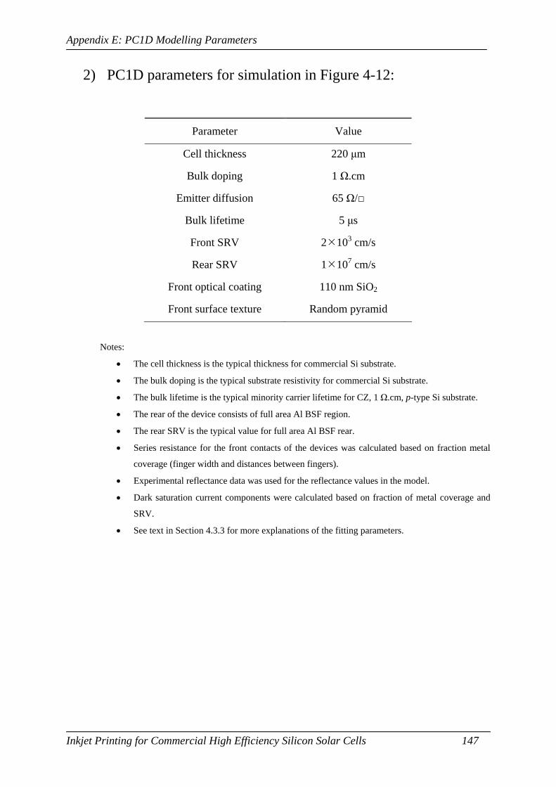
Appendix E: PC1D Modelling Parameters
Inkjet Printing for Commercial High Efficiency Silicon Solar Cells 147
2) PC1D parameters for simulation in Figure 4-12:
Parameter Value
Cell thickness 220 μm
Bulk doping 1 Ω.cm
Emitter diffusion 65 Ω/
Bulk lifetime 5 μs
Front SRV 2 103 cm/s
Rear SRV 1 107 cm/s
Front optical coating 110 nm SiO2
Front surface texture Random pyramid
Notes:
• The cell thickness is the typical thickness for commercial Si substrate.
• The bulk doping is the typical substrate resistivity for commercial Si substrate.
• The bulk lifetime is the typical minority carrier lifetime for CZ, 1 Ω.cm, p-type Si substrate.
• The rear of the device consists of full area Al BSF region.
• The rear SRV is the typical value for full area Al BSF rear.
• Series resistance for the front contacts of the devices was calculated based on fraction metal
coverage (finger width and distances between fingers).
• Experimental reflectance data was used for the reflectance values in the model.
• Dark saturation current components were calculated based on fraction of metal coverage and
SRV.
• See text in Section 4.3.3 for more explanations of the fitting parameters.

Appendix F: General Approach of Liquid Dopant Formulation
Inkjet Printing for Commercial High Efficiency Silicon Solar Cells 148
Appendix F: General Approach of Liquid Dopant
Formulation
H3PO4 (85%) represents the highest possible concentration for a liquid-phase phosphorus-
containing solution. Increasing the H3PO4 concentration above this value, results in the H3PO4
dehydrating to phosphorus pentoxide (P2O5). H3PO4 is also an acidic solution that potentially
poses a compatibility issue with the printhead, especially at highly concentrated levels. But
the main objective of reformulation was to create a solution that can produce finer features
when inkjet printed onto a substrate and heavy phosphorus diffusions with an appropriate
diffusion profile when thermally treated. Table F-1 lists the general objectives that were
considered during the formulation process.
Parameter General requirements
Acidity Reduce acidity by preferably increasing pH level to neutral for
better fluid-printhead compatibility and longer printhead life.
Purity The phosphorus compound must not contain any trace of
metal or organic to ensure high quality junction formation.
Particle size Preferably no particles or very fine particles less than 1 μm in
diameter.
Viscosity and surface
tension
Viscosity and surface tension values that are similar to the
optimum values for the printhead, preferably in the upper
range to reduce droplet spreading.
Solubility Phosphorus-containing compound must be completely soluble
in the solvent used.
Table F-1: General requirements on the formulation of inkjet-printable liquid
phosphorus dopant sources.
For phosphate (PO4)-based compounds, there are two general types of liquid phosphorus
dopant sources: inorganic acid-based and polymer-based solutions. The acid-based solution is
formulated through the reaction of elemental molecules with PO4, whereas the polymer-based

Appendix F: General Approach of Liquid Dopant Formulation
Inkjet Printing for Commercial High Efficiency Silicon Solar Cells 149
solution utilises polymer molecules instead. In order to achieve the highest possible
phosphorus solid content in the final solution, acid-based formulations are preferable than
polymer-based formulations due to the use of lower molecular weight compounds.
In the acid-based formulation, it is clear that H3PO4 would contain the highest phosphorus
solid content possible due to the use of hydrogen atoms, which are the lightest element in the
periodic table. However, in order to reduce the acidity of the solution, the hydrogen needs to
be replaced with another atom or molecule, which will inevitably be larger than hydrogen.
Therefore, any modification away from the structure of H3PO4 would always result in lower
phosphorus solid content.
The method of finding the right molecular substitute to hydrogen to balance the charge of the
PO43- ion is largely an experimental exercise. However, there is a general tendency that pH is
increased with decreasing phosphorus concentration. By examining the available elements
across the periodic table, and keeping in mind the general requirements as set out in Table F-
1, it is possible to narrow down a small number of potentially suitable compounds. It is, of
course, desirable to select a compound that contains as high phosphorus solid content as
possible whilst retaining a liquid formation.
Once a suitable compound has been selected, it is very important to evaluate the solubility of
the compound in a high boiling point solvent while still satisfying the viscosity and surface
tension requirements. Finding a single solvent that would suit all of these requirements is
evidently difficult. As a result, a combination of solvents is usually employed. The solvent
with the highest concentration in the solution is the designated dissolving solvent, which
should provide most, if not all, of the solubility. Sometimes smaller amounts of a second
dissolving solvent are added to improve the solubility of the phosphorus compound. Finally,
extra chemicals may be added in order to adjust the viscosity and surface tension values of the
final solution to within the desired optimal range.
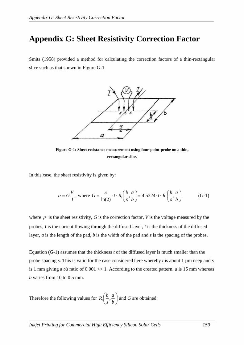
Appendix G: Sheet Resistivity Correction Factor
Inkjet Printing for Commercial High Efficiency Silicon Solar Cells 150
Appendix G: Sheet Resistivity Correction Factor
Smits (1958) provided a method for calculating the correction factors of a thin-rectangular
slice such as that shown in Figure G-1.
Figure G-1: Sheet resistance measurement using four-point-probe on a thin,
rectangular slice.
In this case, the sheet resistivity is given by:
IVG=ρ , where ⎟
⎠⎞
⎜⎝⎛⋅⋅=⎟
⎠⎞
⎜⎝⎛⋅⋅=
ba
sbRt
ba
sbRtG ll ,5324.4,
)2ln(π (G-1)
where ρ is the sheet resistivity, G is the correction factor, V is the voltage measured by the
probes, I is the current flowing through the diffused layer, t is the thickness of the diffused
layer, a is the length of the pad, b is the width of the pad and s is the spacing of the probes.
Equation (G-1) assumes that the thickness t of the diffused layer is much smaller than the
probe spacing s. This is valid for the case considered here whereby t is about 1 µm deep and s
is 1 mm giving a t/s ratio of 0.001 << 1. According to the created pattern, a is 15 mm whereas
b varies from 10 to 0.5 mm.
Therefore the following values for ⎟⎠⎞
⎜⎝⎛
ba
sbRl , and G are obtained:

Appendix G: Sheet Resistivity Correction Factor
Inkjet Printing for Commercial High Efficiency Silicon Solar Cells 151
b (mm) b/s a/b R1 G
10 10 1.5 0.935 4.24
8 8 1.875 0.905 4.10
6 6 2.5 0.840 3.81
4 4 3.75 0.710 3.22
2 2 7.5 0.425 1.93
1 1 15 0.220 1.00
0.5 0.5 30 b/s too small N/A
Table G-1: Sheet resistivity correction factors.
Using measured voltages V for a fixed current I on the different-sized diffused pads and
multiplying the V/I with the correction factors G as given in Table G-1 according to the pad
width (size), the actual measured sheet resistivities can be calculated.

Inkjet Printing for Commercial High Efficiency Silicon Solar Cells 152
Appendix H: List of Author’s Publications
Utama R. Y., Lennon A., Wenham S. R., and Ho-Baillie A. W. Y. 2008, “Methods of
Forming Openings in Selected Materials”, Intl. PCT Publication No. WO/2008/092186.
Lennon A. J., Utama R. Y., Lenio M. A. T., Ho-Baillie A. W. Y., Kuepper N. B., and
Wenham S. R. 2008, “Forming openings to semiconductor layers of silicon solar cells by
inkjet printing” Solar Energy Materials and Solar Cells, Vol. 92, No. 11, pp. 1410-1415.
Utama R., Lennon A., Lenio M., Borojevic N., Ho-Baillie A., Karpour A., and Wenham S.
R. 2008, “Inkjet printing for high efficiency selective emitter silicon solar cell”, 23rd
European Photovoltaic Solar Energy Conference and Exhibition (Valencia).
Borojevic N., Ho-Baillie A., Utama R., Lennon A., Lenio M., Karpour A., and Wenham S.
2008, “Inkjet texturing for high efficiency commercial silicon solar cells”, 23rd European
Photovoltaic Solar Energy Conference and Exhibition (Valencia).
Lennon A., Utama R., Ho-Baillie A., and Wenham S. 2008, “Inkjet method for direct
patterned etching of silicon dioxide” DF 2008 International Conference on Digital
Fabrication Technologies (Pittsburgh).
Utama R., Lennon A., Ho-Baillie A., Lenio M., Borojevic N., and Wenham S. 2007, “Inkjet
printing for high efficiency silicon solar cell structures”, 17th International Photovoltaic
Science and Engineering Conference (Fukuoka).
Kuepper N., Utama R., Guo A., Wells M., Ho A. W. Y., and Wenham S. R. 2007,
“Photovoltaic technology for developing countries” 22nd European Photovoltaic Solar Energy
Conference and Exhibition (Milan).
Lennon A., Utama R., Ho-Baillie A., Lenio M., Kuepper N., and Wenham S. 2007, “Inkjet
method for forming openings to buried semiconductor layers of silicon solar cells”, DF 2007
International Conference on Digital Fabrication Technologies (Anchorage).