infrastructure of thin films laboratory in institute of
TRANSCRIPT

Infrastructure of Thin Films Laboratory in
Institute of Molecular PhysicsPolish Academy of Sciences

Outline
• Sample preparation
• Magnetron sputtering
• Ion-beam sputtering
• Pulsed laser deposition
• Electron-beam litography
• Structural characterization
• SEM – Scanning Electron Microscopy
• XRR – X-ray Reflectometry
• XRD – X-ray Diffraction
• XRF – X-ray Fluorescence
• Profilometer

Outline
• Static magnetic measurements
• VSM – Vibrating Sample Magnetometer
• GMR – Giant Magneto Resistance
• P-MOKE Magnetometer
• P-MOKE Microscopy
• Dynamic magnetic measurements
• VNA-FMR – Vector Network Analizer – Ferromagnetic
Resonance
• FMR – Ferromagnetic Resonance
• PIMM – Pulsed inductive microwave magnetometer

UHV system
Ion-beam sputtering
Sample storage
Pulsed laser deposition
Distribution chamber
Magnetron sputtering

Magnetron sputterings
• Base pressure <5x10⁻⁹ mbar• Up to 6 ultrapure 2 inche targets• Possibility to prepare multilayer systems or alloys
(confocal setup)• Possible to make wedge layers • Sample size - up to 15x20mm

Ion-beam sputtering
• Base pressure <5x10⁻⁹ mbar• Up to 4 ultrapure 2 inches targets • Sample size up to 15x20mm• Two ion sources – for sputter and etching• Mass spectrometer

Pulsed laser deposition
• Base pressure <5x10⁻⁹ mbar• Up to 6 ultrapure 1 inch targets• Sample size up to 15x20mm• Ion source – for etching
Laser:• 1064 nm – IR – 2.55 J• 532 nm – Green – 1.65 J• 355 nm – UV – 0.85 J• 266 nm – UV – 0.23 J

Electron-beam litography
- Preparation of samples in CleanRoom class 1000- PMMA and MMA electron resists in thickness
range from ~50nm to a few microns- Max. wafer size - 150mm (6in.)

SEM
With FEI Nova NanoSEM 650 we can:
• Expand our research capabilities by handling a wider range of sample types
• Perform high resolution imaging - low voltage [1kV] resolution is 1.8nm in low vacuum mode and 1.4 nm in high vacuum mode, so we can still use all the benefits offered by low vacuum imaging without having to sacrifice resolution in images
• Both a high current beam (essential for rapid EDS/EBSD/CL/analytical research) and high resolution at high and low voltage which is essential for image quality across a wide range of sample type are available
Moreover our system includes:
• Bruker EDS system• Raith litography system

XRR/XRD
Seifert, model XRD 3003, X-ray source Cu-K (wavelength λ=0.15419 nm)
X-ray source
sample
detector
aperture
Allows to measure thickness and structure of thin films
2θ varies 0o - 10o
Interference of the wave reflected from surface of the film and the surface of the substrate results in Kiessig fringes.

XRF
• We can measure:– Thickness of thin films (up to 200 nm)– Chemical composition
1 – X-ray source, 2 - collimator, 3 – sample holder, 4 - detector
Multichannel analyzer 10 keV / 1024 channels
Characteristic radiation

Profilometer
• Measurement Technique - Stylus profilometry (contact measurement)
• Measurement Capability - Two-dimensional surface profile measurements
• Stylus Force – 0,03 to 15 mg with LIS 3 sensor• Stylus Options - Stylus radius from 50nm to 25µm• Scan Length Range - 55mm (2 in.)• Max. Sample Thickness - 50mm (1.95 in.)• Max. Wafer Size - 200mm (8 in.)• Step Height Repeatability <5 Å, 1 sigma on 0.1 μm step• Vertical Resolution – 1 Å max. (@ 6.55 μm range)
BRUKER – Dektak XT

VSM
• Frequency: 35 Hz
• Dual pickup coils
• Magnetic field: up to 16 kOe
• Temperature: -100oC to 250oC
Generator
Gaussmeter
Pickup coils
Power supply
Lock-in
Hallotron
Glass pipe
Loudspeaker
PC

GMR
• Four point probe (4 pins)
resistivity measurements (2
current / 2 voltage) with
magnetic field up to 16 kOe
• Possibility to measure in coils
using 11 points (2 current / 9
voltage - for wedge samples)
with magnetic field up to 0.3 kOe
• Current source 100 nA – 100 uA

P-MOKE
Wavelength λ=640 nm

P-MOKE1. Laser diode2. Polarizer3. Modulator4. Lens 5. Electromagnet6. Sample holder and table7. Mirror8. Analyser9. Lens10. Detector (fotodiode)11. Magnetic field sensor
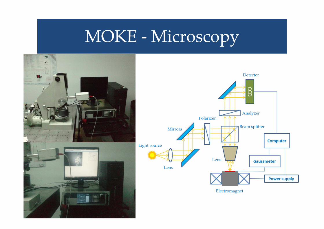
MOKE - Microscopy
Beam splitter
AnalyzerPolarizer
Mirrors
Lens
Light source
Lens
Electromagnet
Detector

VNA-FMR
Frequency up to 40 GHz
Port 1 Port 2
Sample
External magnetic field
Microwave field
Coplanarwaveguide
On frequency sweep FMR experiment
magnetization vector does not change its
direction

VNA-FMR
VNA
Gaussmeter
Helmholtz’scoils
Power supply

FMR
During field sweep FMR experiment magnetization vector changes its direction

FMR
Lock-in
Gaussmeter
Microwave bridge
Field sweepcontroller
• X-band spectrometer 9.18 GHz
• Field up to 11 kOe
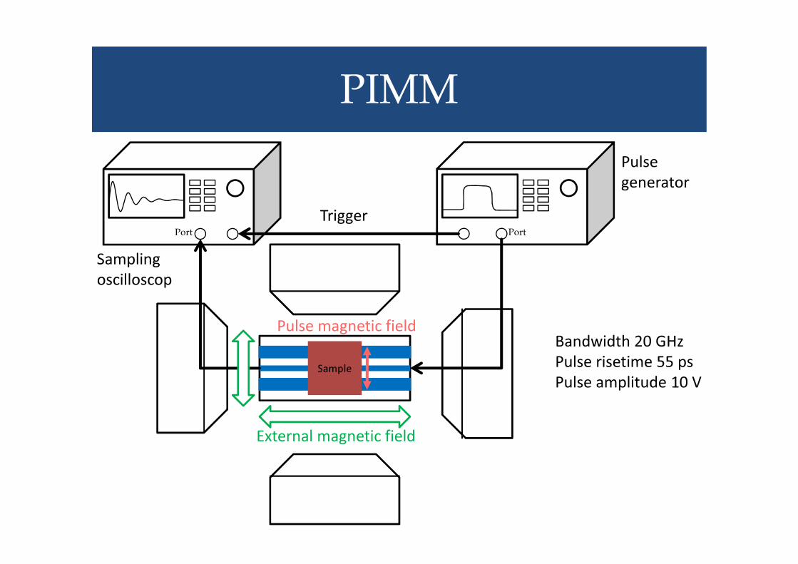
PIMM
Port
Sample
External magnetic field
Pulse magnetic field
Port
Pulse generator
Samplingoscilloscop
Trigger
Bandwidth 20 GHzPulse risetime 55 psPulse amplitude 10 V

PIMM
Pulse generator
Oscilloscop
Power supply
Helmholtz’s coils