infrared thermopile sensor with integrated math engine ... sheets/texas...v+ agnd dgnd 16-bit adc...
TRANSCRIPT
V+
AGND DGND
16-BitADC
Gain
LocalTemperatureIR
ThermopileSensor
VoltageReference
DigitalControl
andMath Engine
I2C and SMBus
CompatibleDigital
Interface
ALERTADR0ADR1SCLSDA
TMP007
EEPROM
Thot
TcoldThot
Thot
Thot
+
Product
Folder
Sample &Buy
Technical
Documents
Tools &
Software
Support &Community
An IMPORTANT NOTICE at the end of this data sheet addresses availability, warranty, changes, use in safety-critical applications,intellectual property matters and other important disclaimers. PRODUCTION DATA.
TMP007SBOS685C –APRIL 2014–REVISED JULY 2015
TMP007 Infrared Thermopile Sensor with Integrated Math Engine
1
1 Features1• Integrated MEMS Thermopile for Noncontact
Temperature Sensing• 14-Bit Local Temperature Sensor for Cold
Junction Reference– ±1°C (max) from 0°C to +60°C– ±1.5°C (max) from –40°C to +125°C
• Integrated Math Engine– Directly Read Object Temperature– Programmable Alerts– Nonvolatile Memory for Storing Calibration
Coefficients– Transient Correction
• Two-Wire Serial Interface Options– I2C and SMBus Compatible– Eight Programmable Addresses
• Low Power– Supply: 2.5 V to 5.5 V– Active Current: 270 μA (typ)– 2-µA Shutdown (max)
• Compact Package– 1.9-mm × 1.9-mm × 0.625-mm DSBGA
2 Applications• Noncontact Temperature Sensing
– Case Temperature– Laser Printers– Power Relays– Health and Beauty– HVAC Comfort Optimization
• Gas Concentration• Flame Detection
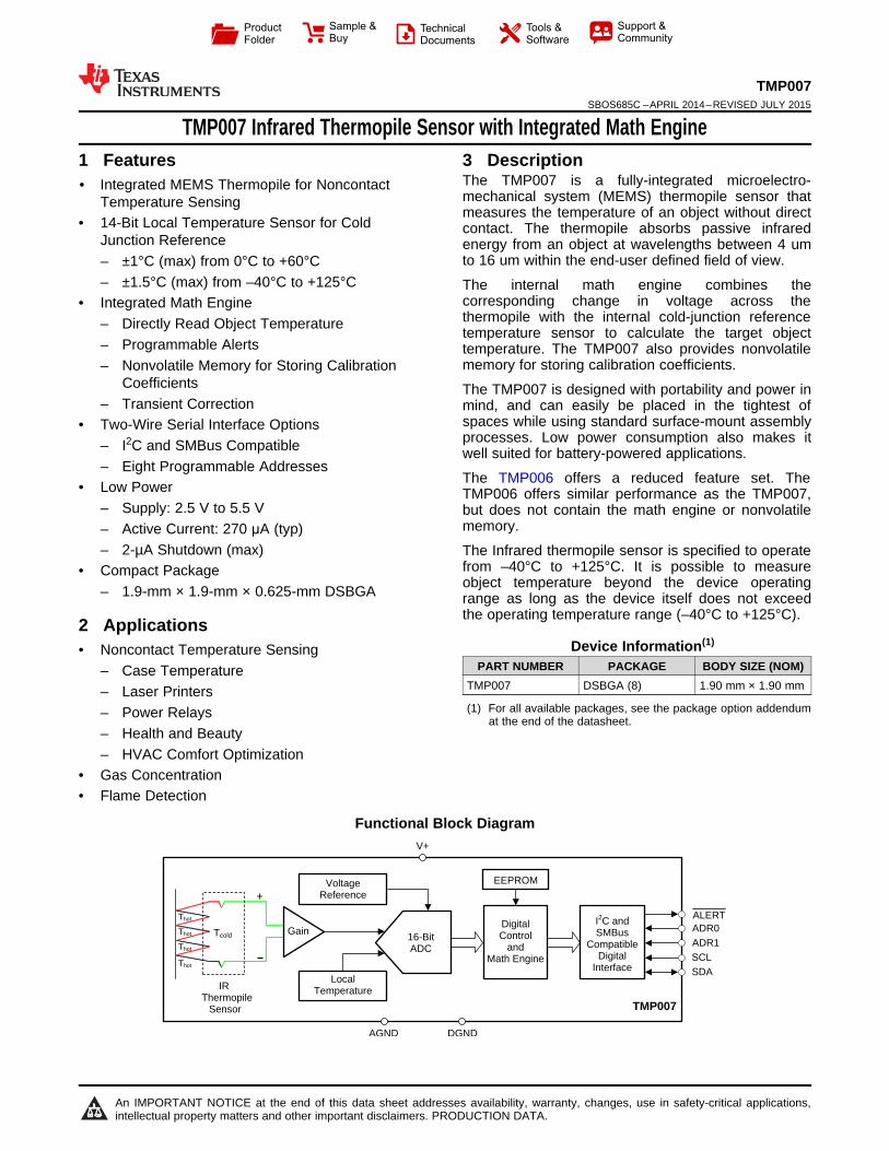
3 DescriptionThe TMP007 is a fully-integrated microelectro-mechanical system (MEMS) thermopile sensor thatmeasures the temperature of an object without directcontact. The thermopile absorbs passive infraredenergy from an object at wavelengths between 4 umto 16 um within the end-user defined field of view.
The internal math engine combines thecorresponding change in voltage across thethermopile with the internal cold-junction referencetemperature sensor to calculate the target objecttemperature. The TMP007 also provides nonvolatilememory for storing calibration coefficients.
The TMP007 is designed with portability and power inmind, and can easily be placed in the tightest ofspaces while using standard surface-mount assemblyprocesses. Low power consumption also makes itwell suited for battery-powered applications.
The TMP006 offers a reduced feature set. TheTMP006 offers similar performance as the TMP007,but does not contain the math engine or nonvolatilememory.
The Infrared thermopile sensor is specified to operatefrom –40°C to +125°C. It is possible to measureobject temperature beyond the device operatingrange as long as the device itself does not exceedthe operating temperature range (–40°C to +125°C).
Device Information(1)
PART NUMBER PACKAGE BODY SIZE (NOM)TMP007 DSBGA (8) 1.90 mm × 1.90 mm
(1) For all available packages, see the package option addendumat the end of the datasheet.
Functional Block Diagram

2
TMP007SBOS685C –APRIL 2014–REVISED JULY 2015 www.ti.com
Product Folder Links: TMP007
Submit Documentation Feedback Copyright © 2014–2015, Texas Instruments Incorporated
Table of Contents1 Features .................................................................. 12 Applications ........................................................... 13 Description ............................................................. 14 Revision History..................................................... 25 Pin Configuration and Functions ......................... 46 Specifications......................................................... 5
6.1 Absolute Maximum Ratings ...................................... 56.2 ESD Ratings.............................................................. 56.3 Recommended Operating Conditions....................... 56.4 Thermal Information ................................................. 56.5 Electrical Characteristics........................................... 66.6 Typical Characteristics .............................................. 7
7 Detailed Description ............................................ 107.1 Overview ................................................................. 107.2 Functional Block Diagram ....................................... 107.3 Feature Description................................................. 107.4 Device Functional Modes........................................ 23
7.5 Register Maps ........................................................ 268 Application and Implementation ........................ 36
8.1 Application Information............................................ 368.2 Typical Applications ................................................ 368.3 System Examples ................................................... 43
9 Power-Supply Recommendations...................... 4410 Layout................................................................... 45
10.1 Layout Guidelines ................................................. 4510.2 Layout Examples................................................... 46
11 Device and Documentation Support ................. 4811.1 Device Support .................................................... 4811.2 Documentation Support ........................................ 4811.3 Community Resources.......................................... 4811.4 Trademarks ........................................................... 4811.5 Electrostatic Discharge Caution............................ 4811.6 Glossary ................................................................ 48
12 Mechanical, Packaging, and OrderableInformation ........................................................... 49
4 Revision HistoryNOTE: Page numbers for previous revisions may differ from page numbers in the current version.
Changes from Revision B (May 2014) to Revision C Page
• Changed Features, Applications, and Description sections ................................................................................................... 1• Changed thermopile sensor portion of functional block diagram ........................................................................................... 1• Changed Handling Ratings to ESD Ratings and moved storage temperature to Absolute Maximum Ratings ..................... 5• Added "full angle" to clarify field of view parameter in Electrical Characteristics................................................................... 6• Changed Figure 2................................................................................................................................................................... 7• Changed thermopile sensor portion of functional block diagram ......................................................................................... 10• Deleted last sentence from 2nd paragraph of Field of View and Angular Response section .............................................. 12• Added Figure 20 .................................................................................................................................................................. 12• Changed text in Thermopile Principles and Operation section to clarify temperature measurement ................................. 13• Changed value in Stefan-Boltzman constant definition from 5.7 to 5.67 in Equation 5 ...................................................... 14• Changed C to C2 in Table 1................................................................................................................................................. 14• Changed recalibration item 3 in Calibration section ............................................................................................................. 15• Changed recalibration item 8 in Calibration section ............................................................................................................. 15• Added Sensor Voltage Format section................................................................................................................................. 16• Added Temperature Format section..................................................................................................................................... 17• Changed text in Temperature Format section to clarify temperature conversion to degrees Celsius ................................. 17• Changed text in Slave Receiver Mode section..................................................................................................................... 19• Changed text in Slave Transmitter Mode section................................................................................................................. 19• Changed Figure 24 to clarify timing...................................................................................................................................... 21• Changed incorrect SDA timing in Figure 25......................................................................................................................... 22• Changed SDA timing in Figure 26 ....................................................................................................................................... 22• Changed register names in Table 7 to match registers in the rest of document. ............................................................... 26• Changed register 2 reset value ............................................................................................................................................ 26• Changed C coefficient to C2 coefficient in Table 7 .............................................................................................................. 26• Added Manufacturer ID register ........................................................................................................................................... 26

3
TMP007www.ti.com SBOS685C –APRIL 2014–REVISED JULY 2015
Product Folder Links: TMP007
Submit Documentation FeedbackCopyright © 2014–2015, Texas Instruments Incorporated
Revision History (continued)• Added missing numbers (3, 2, and 1) to bit descriptions for A1, A2, B0, B1, and B2. ........................................................ 27• Changed register names in Table 8 to match register names in rest of document ............................................................. 27• Changed C coefficient to C2 coefficient in Table 8 .............................................................................................................. 27• Changed Figure 31 bit register to show correct bit names................................................................................................... 28• Changed Figure 32 bit register reset values ........................................................................................................................ 28• Added TOBJ to all Object Temperature titles in data sheet .................................................................................................. 29• Changed Figure 36 to Figure 39 bit register descriptions to show correct bit names.......................................................... 31• Changed Figure 40 bit register reset values ........................................................................................................................ 32• Deleted "Twos complement format" from S0 bit description ............................................................................................... 32• Changed Figure 41 bit register reset values ........................................................................................................................ 32• Changed Figure 42 bit register reset values ........................................................................................................................ 32• Changed C to C2 in C2 Coefficient Register section ........................................................................................................... 33• Added Manufacturer ID register ........................................................................................................................................... 34• Changed Figure 50 bit register names and reset values ..................................................................................................... 34• Changed bit names in Figure 51 to match the text shown in Table 8.................................................................................. 35• Changed bit names in Figure 52 to match the text shown in Table 8.................................................................................. 35• Changed capacitor in Figure 53 from 0.01 µF to 0.1 µF ...................................................................................................... 36• Changed capacitor in Figure 56 from 0.01 µF to 0.1 µF ...................................................................................................... 40• Changed σB to σ in Equation 20 to show correct Stefan-Boltzmann symbol ...................................................................... 43• Changed symbol for Stefan-Boltzmann constant from B to σ in Equation 20 ..................................................................... 43• Changed decoupling capacitor in Power-Supply Recommendations section from 0.01 µF to 0.1 µF ................................. 44• Changed title for Figure 61 .................................................................................................................................................. 46• Deleted Figure 63, Bottom Layer ........................................................................................................................................ 47
Changes from Revision A (May 2014) to Revision B Page
• Changed Absolute Maximum Ratings operating temperature range parameter min value from –40 to –55......................... 5• Added operating temperature range parameter to Recommended Operating Conditions .................................................... 5• Changed the POR registers in Figure 32 ............................................................................................................................ 28• Added OLF bit to status register, Figure 34 ........................................................................................................................ 29• Changed OHF bit to status register, Figure 34 ................................................................................................................... 29• Changed Table 9 .................................................................................................................................................................. 32• Changed the POR registers in Figure 40 through Figure 48................................................................................................ 32• Changed the POR registers in Figure 50 and Figure 52...................................................................................................... 34• Changed Table 14 header row titles .................................................................................................................................... 40• Changed Table 14 header row titles .................................................................................................................................... 41• Changed Figure 61 .............................................................................................................................................................. 46• Changed Figure 63, Bottom Layer ....................................................................................................................................... 47• Changed Figure 62............................................................................................................................................................... 47
Changes from Original (May 2014) to Revision A Page
• Changed from product preview to production data ............................................................................................................... 1

C1 C3C2
B1 B3
A1 A3A2
Sensor
C
B
A
1 32
Row
s
Columns
4
TMP007SBOS685C –APRIL 2014–REVISED JULY 2015 www.ti.com
Product Folder Links: TMP007
Submit Documentation Feedback Copyright © 2014–2015, Texas Instruments Incorporated
5 Pin Configuration and Functions
YZF Package8-Pin DSBGA
Top View
Pin FunctionsPIN
DESCRIPTIONNAME NO.ADR0 C1 Input address 0 selection pinADR1 B1 Input address 1 selection pinAGND A2 Analog groundALERT C2 Alert output pin; active low, open-drain. Requires a pull-up resistor to (1.6 V to 5.5 V) supplyDGND A1 Digital groundSCL B3 Input clock pinSDA C3 Input/output data pin; open-drain; requires pull-up resistor to (1.6 V to 5.5 V) supplyV+ A3 Supply voltage (2.5 V to 5.5 V)

5
TMP007www.ti.com SBOS685C –APRIL 2014–REVISED JULY 2015
Product Folder Links: TMP007
Submit Documentation FeedbackCopyright © 2014–2015, Texas Instruments Incorporated
(1) Stresses beyond those listed under Absolute Maximum Ratings may cause permanent damage to the device. These are stress ratingsonly, which do not imply functional operation of the device at these or any other conditions beyond those indicated under RecommendedOperating Conditions. Exposure to absolute-maximum-rated conditions for extended periods may affect device reliability.
(2) Input voltage rating applies to all TMP007 input voltages.
6 Specifications
6.1 Absolute Maximum Ratingsover operating free-air temperature range (unless otherwise noted) (1) (2)
MIN MAX UNIT
VoltageSupply voltage, VS 7 V
Input voltageADR1 VS + 0.5 VAll other pins –0.5 +7 V
Current Input current, any pin 10 mA
TemperatureOperating range –40 +125 °CJunction, TJ 125 °CStorage, Tstg –65 +125 °C
(1) JEDEC document JEP155 states that 500-V HBM allows safe manufacturing with a standard ESD control process.(2) JEDEC document JEP157 states that 250-V CDM allows safe manufacturing with a standard ESD control process.
6.2 ESD RatingsVALUE UNIT
V(ESD)Electrostaticdischarge
Human-body model (HBM), per ANSI/ESDA/JEDEC JS-001 (1) ±2000VCharged-device model (CDM), per JEDEC specification JESD22-C101 (2) ±500
Machine model ±200
(1) Object temperature is application dependent.
6.3 Recommended Operating Conditionsover operating free-air temperature range (unless otherwise noted)
MIN NOM MAX UNITSupply voltage, VS 2.5 3.3 5.5 VOperating temperature range –40 +125 °CDie temperature, TDIE 125 °CObject temperature, TOBJ See note (1) °C
(1) For more information about traditional and new thermal metrics, see the IC Package Thermal Metrics application report, SPRA953.
6.4 Thermal Information
THERMAL METRIC (1)TMP007
UNITYZF (DSBGA)8 PINS
RθJA Junction-to-ambient thermal resistance 115.3 °C/WRθJC(top) Junction-to-case (top) thermal resistance 0.4 °C/WRθJB Junction-to-board thermal resistance 14.3 °C/WψJT Junction-to-top characterization parameter 3.8 °C/WψJB Junction-to-board characterization parameter 14.1 °C/WRθJC(bot) Junction-to-case (bottom) thermal resistance N/A °C/W

6
TMP007SBOS685C –APRIL 2014–REVISED JULY 2015 www.ti.com
Product Folder Links: TMP007
Submit Documentation Feedback Copyright © 2014–2015, Texas Instruments Incorporated
(1) This parameter is tested in a fully-settled setup with no transients, in front of a black body, ε = 0.95, field of view (FOV) = 110°, with therecommended layout , and after system calibration with a common set of coefficients loaded.
(2) Average current over complete measurement cycle.
6.5 Electrical Characteristicsat TDIE = 25°C, and V+ = +3.3 V (unless otherwise noted)
PARAMETER TEST CONDITIONS MIN TYP MAX UNIT
DEVICE PERFORMANCE
Responsivity (signal) TDIE = 0°C to 100°C, TOBJ = 0°C to 60°C 9 V/W
Sensor noise 1-s conversion, TDIE = 0°C to 60°C, TOBJ = 0°C to60°C 300 nVrms
Noise equivalent power (NEP) At 1 σ, TDIE = 0°C to 60°C, TOBJ = 0°C to 60°C 32 nW
Noise equivalent temperature difference (1)(NETD) TDIE = 0°C to 60°C, TOBJ = 0°C to 60°C 90 mK
Noise equivalent temperature difference (NETD) At F/1 (6 σ), TDIE = 25°C, TOBJ = 0°C to 60°C 1.4 °C
Absorber size 330 × 330 μm
REFERENCE SYSTEM PERFORMANCE (1)
Object temperature accuracy (1) (error)TDIE = 20°C to 40°C, TOBJ = 20°C to 60°C ±1 ±3 °C
TDIE = 0°C to 60°C, TOBJ = –15°C to 85°C ±2 ±5 °C
TEMPERATURE MEASUREMENT
TDIE Die temperature range –40 +125 °C
TDIE accuracy (error) ±0.5 ±1 °C
Accuracy vs supply ±0.1 ±0.2 °C/V
Conversion time 0.25 Second
Temperature resolution (object and local) 0.03125 °C/LSB
Field of view (50% responsivity, full angle) 90 Degrees
DIGITAL PINS
VIH High-level input voltage 1.4 V
VIL Low-level input voltage 0.4 V
Hysteresis 200 mV
VOL Low-level output voltage, SDA IOUT = –6 mA 0.05 0.4 V
Output ALERT logic low sink IOUT = –6 mA 0.200 V
IIN Input current 0 V < VIN < 5.5 V –1 +1 µA
Input capacitance 3 pF
SMBus frequency 0.01 2.5 MHz
Timeout time 25 28 35 ms
POWER SUPPLY
V+ Operating supply range 2.5 5.5 V
POR Power-on reset 1.9 V
Nonvolatile memory programming voltage 2.5 5.5 V
Nonvolatile memory programming current Supply current pulse time < 3 ms 2.8 mA
IQ Quiescent current
Serial bus inactive, continuous conversion 270 350 µA
Low power conversion, serial bus inactive, CR2 =1, CR1 = x, CR0 = 1 85 (2) µA
Low power conversion serial bus active, CR2 = 1,CR1 = 1, CR0 = 0 60 (2) µA
ISD Shutdown currentSerial bus inactive 2 4 µA
Serial bus active, 400 kHz 36 µA

0
10
20
30
40
50
60
70
0 20 40 60 80
NE
P (
nW)
Object Temperature (�C)
60°C40°C20°C0°C
C010
0
20
40
60
80
100
120
0 20 40 60 80
NE
TD
(m
K)
Object Temperature (�C)
0°C20°C40°C
C011
±400
±300
±200
±100
0
100
200
300
400
±40 ±20 0 20 40
Sen
sor
Vol
tage
(µ
V)
IR Power (µW)
60°C
40°C
20°C
0°C
C007
Responsivity - 9 V/W
0
200
400
600
800
±20 0 20 40 60 80 100
Sen
sor
rms
Noi
se (
nV)
Object Temperature (�C)
60°C40°C20°C0°C
C008
0.0
0.2
0.4
0.6
0.8
1.0
1.2
4.0 8.0 12.0 16.0
Rel
ativ
e R
espo
nse
Wavelength (µm) C005
20
30
40
50
60
70
80
90
100
110
±90 ±75 ±60 ±45 ±30 ±15 0 15 30 45 60 75 90
Res
pons
ivity
(%
)
Angle (�) C001
Field of View
7
TMP007www.ti.com SBOS685C –APRIL 2014–REVISED JULY 2015
Product Folder Links: TMP007
Submit Documentation FeedbackCopyright © 2014–2015, Texas Instruments Incorporated
6.6 Typical Characteristicsat TDIE = 25°C, and V+ = +3.3 V (unless otherwise noted)
Figure 1. Relative Spectral Response vs Wavelength Figure 2. Responsivity vs Angle
NOTE: The responsivity is the slope of the lines.
Figure 3. Sensor Voltage vs IR Power Over TDIE Figure 4. Sensor Noise vs TOBJ and TDIE
Figure 5. NEP vs TOBJ and TDIE Figure 6. NETD for Reference System at F/1 Over TDIE

-3.0
-2.0
-1.0
0.0
1.0
2.0
3.0
0 10 20 30 40 50 60 70 80
Tob
j Acc
urac
y-
Com
mon
Cal
ibra
tion
(�C
)
Object Temperaturej (�C)
0°C C
20°C C
40°C C
60°C C
C018
0.0
0.5
1.0
1.5
2.0
2.5
±50 ±25 0 25 50 75 100 125 150
PO
R (
V)
TDIE (�C) C036
0
5
10
15
20
25
30
35
40
45
50
±50 ±25 0 25 50 75 100 125 150
T D
IE P
SR
R (
m�C
/V)
TDIE (�C)
PSRR
C014
-3.00
-2.00
-1.00
0.00
1.00
2.00
3.00
0 10 20 30 40 50 60 70 80
Tob
j Acc
urac
y -
Uni
t Cal
ibra
tion
(�C
)
Object Temperature (�C)
0°C U20°C U40°C U60°C U
C017
-2.00
-1.50
-1.00
-0.50
0.00
0.50
1.00
1.50
2.00
±50 ±25 0 25 50 75 100 125 150
TD
IE E
rror
(�C
)
TDIE (�C)
Error (°C)��1 -�1
C013
0.0
0.2
0.4
0.6
0.8
1.0
0 1 2 3 4 5 6 7
Rel
ativ
e rm
s N
oise
Conversion Rate Code
Noise 25°C
Noise 75°C
C012
8
TMP007SBOS685C –APRIL 2014–REVISED JULY 2015 www.ti.com
Product Folder Links: TMP007
Submit Documentation Feedback Copyright © 2014–2015, Texas Instruments Incorporated
Typical Characteristics (continued)at TDIE = 25°C, and V+ = +3.3 V (unless otherwise noted)
NOTE: In the last three conversion modes, there is a change insensor voltage, and a different set of calibration coefficients may beneeded depending on the accuracy required.
Figure 7. Sensor Noise at TDIE = 25°C and 75°C vs SampleTime
Figure 8. TDIE Accuracy
2.5 V < VS < 5.5 V
Figure 9. TDIE PSRR vs TDIE Figure 10. Accuracy with Unit Calibration (0°C to 60°C)
Figure 11. Accuracy with Common Calibration (0°C to 60°C) Figure 12. POR Voltage vs TDIE

150
175
200
225
250
275
300
325
350
±50 ±25 0 25 50 75 100 125 150
Sup
ply
Cur
rent
(µ
A)
TDIE (�C)
V = 5.5 VV = 4.4 VV = 3.3 VV = 2.5 V
C039
-1.00
-0.80
-0.60
-0.40
-0.20
0.00
0.20
0.40
0.60
0.80
1.00
±50 ±25 0 25 50 75 100 125 150
Fre
quen
cy D
rift (
%)
TDIE (�C) C040
0.00
0.05
0.10
0.15
0.20
0.25
0.30
0 5 10 15 20 25
Pin
Vol
tage
(V
)
Pin Current (mA)
ALERT pinSDA Pin
C037
0
1
2
3
4
5
±50 ±25 0 25 50 75 100 125 150
Shu
tdow
n C
urre
nt (
µA
)
TDIE (�C)
V = 5.5 VV = 4.4 VV = 3.3 VV = 2.5 V
C039
9
TMP007www.ti.com SBOS685C –APRIL 2014–REVISED JULY 2015
Product Folder Links: TMP007
Submit Documentation FeedbackCopyright © 2014–2015, Texas Instruments Incorporated
Typical Characteristics (continued)at TDIE = 25°C, and V+ = +3.3 V (unless otherwise noted)
Figure 13. Output Pin Voltage vs Current Figure 14. ShutDown Current vs TDIE
Figure 15. Supply Current vs TDIE (Continuous Conversion) Figure 16. Conversion Frequency Stability vs TDIE

( )2
2
5
k TB
2hc 1B T, watts / cm / m
hc
e 1l
æ öç ÷ç ÷l = ml ç ÷lç ÷
-è ø
V+
AGND DGND
16-BitADC
Gain
LocalTemperatureIR
ThermopileSensor
VoltageReference
DigitalControl
andMath Engine
I2C and SMBus
CompatibleDigital
Interface
ALERTADR0ADR1SCLSDA
TMP007
EEPROM
Thot
TcoldThot
Thot
Thot
+
10
TMP007SBOS685C –APRIL 2014–REVISED JULY 2015 www.ti.com
Product Folder Links: TMP007
Submit Documentation Feedback Copyright © 2014–2015, Texas Instruments Incorporated
7 Detailed Description
7.1 OverviewThe TMP007 is an integrated digital thermopile temperature sensor in a wafer chip-scale package (WCSP) thatdetects the temperature of a remote object by its infrared (IR) emission. It is optimal for thermal managementand thermal protection applications where remote noncontact temperature sensing is desired. The TMP007 istwo-wire and SMBus interface compatible, and is specified over the temperature range of –40°C to 125°C. TheTMP007 contains registers for holding configuration and calibration information, temperature limits, localtemperature, TDIE, measurement results, and the thermopile voltage measurement result. The local temperatureand the thermopile voltage measurements are used by the math engine to calculate the object temperature,which is then stored in the respective register. In addition, the TMP007 has an internal EPROM memory that canbe used to store the factory default values and custom values for coefficients and calibration parameters. Thevalues in EPROM can be transferred to the registers either individually or as a complete set.
The SDA (and SCL, if driven by an open-drain output) interface pin requires a pull-up resistor (10 kΩ, typical) aspart of the communication bus. The ALERT pin is an open-drain output that must also use a pull-up resistor, orbe left floating if unused. If desired, ALERT may be shared with other devices for a wired-OR implementation.
7.2 Functional Block Diagram
7.3 Feature DescriptionThe TMP007 senses the IR radiation that is emitted by all objects. The spectrum of the radiation depends onlyon the temperature and is given by Planck’s law, as shown in Equation 1:
where• h = Planck’s constant• c = speed of light• kB = Boltzmann’s constant• λ = wavelength in microns (1)

0.0
0.2
0.4
0.6
0.8
1.0
1.2
4.0 8.0 12.0 16.0
Rel
ativ
e R
espo
nse
Wavelength (µm) C005
0.000
0.005
0.010
0.015
0.020
0.025
0 5 10 15 20
Spectr
alR
adia
nt
Exitance
(W/(
cm
m)
μ2
Wavelength (µm)
450 K400 K350 K300 K250 K
C019
16 µm4 µm
11
TMP007www.ti.com SBOS685C –APRIL 2014–REVISED JULY 2015
Product Folder Links: TMP007
Submit Documentation FeedbackCopyright © 2014–2015, Texas Instruments Incorporated
Feature Description (continued)The intensity of radiation from the object is determined by the emisivity (ε), a material-dependent property thatscales the spectral response so that 0 < ε < 1. For an ideal black body, the radiation is at a maximum for a giventemperature and ε = 1. The temperature is measured on the Kelvin scale where 0 K is absolute zero, or–273.15°C. Room temperature (25°C) is approximately 298.13 K. The emission spectra for objects at or nearroom temperature are shown in Figure 17. For these temperatures, the majority of the radiation emitted is in thewavelength range of 3 µm to 20 µm.
Figure 17. Black Body Emission Spectrum and Response
7.3.1 Spectral ResponsivityThe TMP007 is optimized to sense IR radiation emitted by objects from approximately 250 K (–23°C) to 400 K(127°C), with maximum sensitivity from approximately 4 µm to 16 µm. The relative spectral response of theTMP007 is shown in Figure 18.
Figure 18. Relative Spectral Response vs Wavelength

Sensor
1.9 mm
0.33 mm
0.33 mm
0.165 mm
0.165 mm
1.9 mm
TMP007
Object D
-
d
Sensor
12
TMP007SBOS685C –APRIL 2014–REVISED JULY 2015 www.ti.com
Product Folder Links: TMP007
Submit Documentation Feedback Copyright © 2014–2015, Texas Instruments Incorporated
Feature Description (continued)7.3.2 Field of View and Angular ResponseThe TMP007 senses all radiation within a defined field of view (FOV). The FOV (or full-angle of θ) is defined as2Φ. The TMP007 contains no optical elements, and thus senses all radiation within the hemisphere to the front ofthe device. Figure 2 shows the angular dependence of the sensor response and the relative power for a circularobject that subtends a half angle of phi (Φ). Figure 19 defines the angle Φ in terms of object diameter anddistance. Figure 19 assumes that the object is well approximated as a plane that is perpendicular to the sensoraxis.
Figure 19. FOV Geometry Definition
In this case, the maximum contribution is from the portion of the object directly in front of the TMP007 (Φ = 0),with the sensitivity per solid angle, dR/dΦ decreases as Φ increases. Approximately 50% of the energy sensedby the TMP007 is within a FOV (θ) = 90°.
This discussion is for illustrative purposes only; in practice the angular response (dR/dΦ) of the TMP007 to theobject is affected by the object orientation, the number of objects, and the precise placement relative to theTMP007. Figure 20 shows the thermopile sensor dimensions.
NOTE: Thermopile sensor is centered in the device.
Figure 20. Thermopile Sensor Dimensions

N
SENSOR X
X 1
1V Sensor Conversion
N =
= å
N
DIE XX 1
1T Local Temp Conversion
N =
= å
OUT SENSOR HOT COLD OBJ DIEV V C (T T ) (T 4 T 4)= = ´ - µ -
Thermopile
Heat Absorbor Cold Junction
Thot
TcoldThot
Thot
Thot
EHOT ß TDIE 4
EOBJ ß TOBJ 4
+
13
TMP007www.ti.com SBOS685C –APRIL 2014–REVISED JULY 2015
Product Folder Links: TMP007
Submit Documentation FeedbackCopyright © 2014–2015, Texas Instruments Incorporated
Feature Description (continued)7.3.3 Thermopile Principles and OperationThe TMP007 senses radiation by absorbing the radiation on a hot junction. The thermopile then generates avoltage proportional to the temperature difference between the hot junction, Thot, and the cold junction, Tcold.
Figure 21. Principle of Thermopile Operation
The cold junction is thermally grounded to the die, and is effectively TDIE, the die temperature. In thermalequilibrium, the hot junction is determined by the object temperature, TOBJ. The energy emitted by the object,EOBJ, minus the energy radiated by the die, EDIE, determines the temperature of the hot junction. The outputvoltage, VOUT, is therefore determined by the relationship shown in Equation 2:
where• C is a constant depending on the design of the sensing element. (2)
Note that the sensor voltage is related to both the object temperature and the die temperature. A fundamentalcharacteristic of all thermopiles is that they measure temperature differentials, not absolute temperatures. TheTMP007 contains a highly-accurate, internal temperature sensor to measure TDIE. Knowing TDIE and VSENSORenables the TMP007 to estimate TOBJ. For each 250-ms conversion cycle, the TMP007 measures a value forVSENSOR and for TDIE, calculates TOBJ, and then places the values in the respective registers.
Bits CR2 to CR0 determine the number of local and sensor analog-to-digital converter (ADC) results to averagebefore the object temperature is calculated.
After power-on reset (POR), the TMP007 starts in four conversions per second (mode 010). In general, for amode with N conversions, the local temperature, TDIE, result is updated at the end of the Nth ADC conversionwith the value shown in Equation 3:
(3)
Similarly, the sensor voltage result is updated at the end of the Nth sensor ADC conversion with the value shownin Equation 4:
(4)
These results are then used in the object temperature calculation by the math engine, which updates the objecttemperature result register. The total conversion time and averages per conversion can be optimized to selectthe best combination of update rate versus noise for an application. Additionally, low-power conversion mode isavailable. In CR settings 101, 110, and 111, the device inserts a standby time before the beginning of the nextconversion or conversions.
The method and requirements for estimating TOBJ are described in the next section.
{ }4OBJ4
OBJ DIE
ƒ VT T
S
æ ö= + ç ÷ç ÷
è ø
44 SENSOR
OBJ DIE
VT T= +
es
( )4 4
SENSOR ABSORBED RADIATED OBJ DIEV E E T Tµ - = es -
4Rad OBJEnergy T= es
14
TMP007SBOS685C –APRIL 2014–REVISED JULY 2015 www.ti.com
Product Folder Links: TMP007
Submit Documentation Feedback Copyright © 2014–2015, Texas Instruments Incorporated
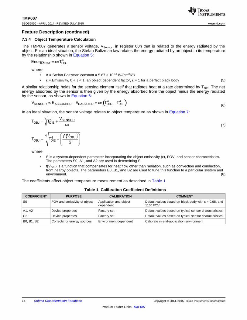
Feature Description (continued)7.3.4 Object Temperature CalculationThe TMP007 generates a sensor voltage, VSensor, in register 00h that is related to the energy radiated by theobject. For an ideal situation, the Stefan-Boltzman law relates the energy radiated by an object to its temperatureby the relationship shown in Equation 5:
where• σ = Stefan-Boltzman constant = 5.67 × 10⁻¹² W/(cm2K4)• ε = Emissivity, 0 < ε < 1, an object dependent factor, ε = 1 for a perfect black body (5)
A similar relationship holds for the sensing element itself that radiates heat at a rate determined by TDIE. The netenergy absorbed by the sensor is then given by the energy absorbed from the object minus the energy radiatedby the sensor, as shown in Equation 6:
(6)
In an ideal situation, the sensor voltage relates to object temperature as shown in Equation 7:
(7)
where• S is a system-dependent parameter incorporating the object emissivity (ε), FOV, and sensor characteristics.
The parameters S0, A1, and A2 are used in determining S.• f(VOBJ) is a function that compensates for heat flow other than radiation, such as convection and conduction,
from nearby objects. The parameters B0, B1, and B2 are used to tune this function to a particular system andenvironment. (8)
The coefficients affect object temperature measurement as described in Table 1.
Table 1. Calibration Coefficient DefinitionsCOEFFICIENT PURPOSE CALIBRATION COMMENT
S0 FOV and emissivity of object Application and objectdependent
Default values based on black body with ε = 0.95, and110° FOV
A1, A2 Device properties Factory set Default values based on typical sensor characteristicsC2 Device properties Factory set Default values based on typical sensor characteristicsB0, B1, B2 Corrects for energy sources Environment dependent Calibrate in end-application environment

15
TMP007www.ti.com SBOS685C –APRIL 2014–REVISED JULY 2015
Product Folder Links: TMP007
Submit Documentation FeedbackCopyright © 2014–2015, Texas Instruments Incorporated
7.3.5 CalibrationThe TMP007 default coefficients are calibrated with a black body of emissivity, ε = 0.95, and an FOV (θ) = 110°.Use these coefficients for applications where the object emissivity and geometry satisfy these conditions. Forapplications with different object emissivity or geometry, calibrate the TMP007 to accurately reflect the objecttemperature and system geometry. Accuracy is affected by device-to-device or object-to-object variation. For themost demanding applications, calibrate each device individually.
As an overview the calibration procedure includes:1. Defining the environmental variation range (die and object temperature range, supply voltage, temperature
change speed, sampling rate and so on).2. Making the die temperature measurements and IR sensor voltage measurements over the environmental
range.3. Generate an optimal set of coefficients based on the collected data set.4. Load the coefficients into the TMP007 coefficients register. The object temperature register reflects the best
fit from the calibration process. Perform validation measurements because accuracy may vary over theenvironmental range. If the object temperature measurement error is not acceptable, repeat the calibrationprocess using more environment points, data averaging, or narrow the temperature range of TDIE or TOBJ.
5. After a suitable set of coefficients is obtained, they can be stored in nonvolatile memory. Each coefficientregister can be programmed up to eight times. After POR, the last stored coefficient value is copied from thenonvolatile memory into the coefficient register.
The best temperature precision is available if every device is calibrated individually. Alternatively, if all the units inthe application use the same coefficients, then calibrate a statistically significant number of devices, and loadaveraged coefficient values in nonvolatile memory.
Recalibration may be required under any or all of the following conditions:1. Board layout changed.2. Object or objects in the field of view changed.3. Object distance or object surface changed.4. Angle between device surface and direction to the object changed.5. Object and local temperature range changed outside the environmental calibration range.6. Object and local temperature transients significantly changed.7. Supply voltage changed more than 1 V.8. Air convection or conduction near the device changed.
For further information and methods for calibration, refer to SBOU142 — TMP007 Calibration Guide.

7FFFh
Outp
ut C
ode
-FS ¼ 0 ¼ FS
Sensor Voltage (AIN AIN )-P N
7FFEh
0001h
¼
0000h
8000h
FFFFh
8001h
¼
-FS2 - 1
15
215
FS2 - 1
15
215
16
TMP007SBOS685C –APRIL 2014–REVISED JULY 2015 www.ti.com
Product Folder Links: TMP007
Submit Documentation Feedback Copyright © 2014–2015, Texas Instruments Incorporated
(1) FS = Full-scale value.
7.3.6 Sensor Voltage FormatThe TMP007 provides 16 bits of data in binary twos complement format. The positive full-scale input produces anoutput code of 7FFFh and the negative full-scale input produces an output code of 8000h. The output clips atthese codes for signals that exceed full-scale. Table 2 summarizes the ideal output codes for different inputsignals. Figure 22 illustrates code transitions versus input voltage. Full-scale is a 5.12-mV signal. The LSB size is156.25 nV.
Table 2. Input Signal Versus Ideal Output Code (1)
SENSOR SIGNAL VOLTAGE OUTPUT CODEFS (215 – 1) / 215 5.12 mV 7FFFh
FS / 215 156.25 nV 0001h0 0 V 0000h
–FS / 215 –156.25 nV FFFFh–FS –5.12 mV 8000h
Figure 22. Code Transition Diagram

17
TMP007www.ti.com SBOS685C –APRIL 2014–REVISED JULY 2015
Product Folder Links: TMP007
Submit Documentation FeedbackCopyright © 2014–2015, Texas Instruments Incorporated
7.3.7 Temperature FormatThe temperature register data format of the TMP007 is reported in a binary twos complement signed integerformat, as Table 3 shows, with 1 LSB = (1 / 32)°C = 0.03125°C.
Table 3. Temperature Data FormatTEMPERATURE (°C) DIGITAL OUTPUT (BINARY) SHIFTED HEX
150 0100 1011 0000 0000 12C0125 0011 1110 1000 0000 0FA0100 0011 0010 0000 0000 0C8080 0010 1000 0000 0000 0A0075 0010 0101 1000 0000 096050 0001 1001 0000 0000 064025 0000 1100 1000 0000 0320
0.03125 0000 0000 0000 0100 00010 0000 0000 0000 0000 0000
–0.03125 1111 1111 1111 1100 FFFF–0.0625 1111 1111 1111 1000 FFFE
–25 1111 0011 0111 0000 FCDC–40 1110 1011 1111 1100 FAFF–55 1110 0100 0111 1100 F91F
To convert the integer temperature result of the TMP007 to degrees Celsius, right-shift the result by two bits.Then perform a divide-by-32 of TDIE and TOBJ, the 14-bit signed integers contained in the correspondingregisters. The sign of the temperature is the same as the sign of the integer read from the TMP007. In twoscomplement notation, the MSB is the sign bit. If the MSB is 1, the integer is negative and the absolute value canbe obtained by inverting all bits and adding 1. An alternate method of calculating the absolute value of negativeintegers is abs(i) = i xor FFFFh + 1.

18
TMP007SBOS685C –APRIL 2014–REVISED JULY 2015 www.ti.com
Product Folder Links: TMP007
Submit Documentation Feedback Copyright © 2014–2015, Texas Instruments Incorporated
7.3.8 Serial InterfaceThe TMP007 operates only as a slave device on the serial bus. Connections to the bus are made using the SCLInput and open-drain I/O SDA line. The SDA and SCL pins feature integrated spike suppression filters andSchmitt triggers to minimize the effects of input spikes and bus noise. The TMP007 supports the transmissionprotocol for both fast and fastplus (1 kHz to 1 MHz) and high-speed (1 MHz to 2.5 MHz) mode. All data bytes aretransmitted MSB first. At higher speeds, thermal dissipation affects device operation, including accuracy.
7.3.8.1 Bus OverviewThe device that initiates a transfer is called a master, and the devices controlled by the master are slaves. Thebus must be controlled by a master device that generates the serial clock (SCL), controls the bus access, andgenerates the start and stop conditions.
To address a specific device, a start condition is initiated, indicated by pulling the data-line (SDA) from a high-to-low logic level while SCL is high. All slaves on the bus shift in the slave address byte, with the last bit indicatingwhether a read or write operation is intended. During the ninth clock pulse, the slave being addressed respondsto the master by generating an Acknowledge and pulling SDA low.
Data transfer is then initiated and sent over eight clock pulses followed by an acknowledge bit. During datatransfer SDA must remain stable while SCL is high, as any change in SDA while SCL is high will be interpretedas a control signal.
Once all data has been transferred, the master generates a stop condition, indicated by pulling SDA from low tohigh while SCL is high.
7.3.8.2 Serial Bus AddressTo communicate with the TMP007, the master must first address slave devices via a slave address byte. Theslave address byte consists of seven address bits, and a direction bit indicating the intent of executing a read orwrite operation. The TMP007 features two address pins allowing up to eight devices to be connected on a singlebus. Pin logic levels and the corresponding address values are described in Table 4.
Table 4. Address Pins and Slave AddressesADR1 ADR0 SMBus ADDRESSES
0 0 10000000 1 10000010 SDA 10000100 SCL 10000111 0 10001001 1 10001011 SDA 10001101 SCL 1000111
7.3.8.3 Writing and Reading OperationsAccessing a particular register on the TMP007 is accomplished by writing the appropriate value to the pointerregister. The value for the pointer register is the first byte transferred after the slave address byte with the R/Wbit low. Every write operation to the TMP007 requires a value for the pointer register (see Figure 24).
When reading from the TMP007, the last value stored in the pointer register by a write operation is used todetermine which register is read by a read operation. To change the register pointer for a read operation, write anew value to the pointer register. This action is accomplished by issuing a slave address byte with the R/W bitlow, followed by the pointer register byte. No additional data are required. The master then generates a startcondition and sends the slave address byte with the R/W bit high to initiate the read command. See Figure 25 fordetails of this sequence. If repeated reads from the same register are desired, it is not necessary to continuallysend the pointer register byte because the TMP007 remembers the pointer register value until it is changed bythe next write operation.
Note that register bytes are sent most significant byte first, followed by the least significant byte.

19
TMP007www.ti.com SBOS685C –APRIL 2014–REVISED JULY 2015
Product Folder Links: TMP007
Submit Documentation FeedbackCopyright © 2014–2015, Texas Instruments Incorporated
7.3.8.4 Slave Mode OperationsThe TMP007 operates as a slave receiver or slave transmitter.
7.3.8.4.1 Slave Receiver Mode
The first byte transmitted by the master is the slave address, with the R/W bit low. The TMP007 thenacknowledges reception of a valid address. The next byte transmitted by the master is the pointer register. TheTMP007 then acknowledges reception of the pointer register byte. The next two bytes are written to the registeraddressed by the pointer register. The TMP007 acknowledges reception of both data bytes. The masterterminates data transfer by generating a start or stop condition.
7.3.8.4.2 Slave Transmitter Mode:
The first byte is transmitted by the master and is the slave address, with the R/W bit high. The TMP007acknowledges reception of a valid slave address. The next two bytes transmitted by the TMP007 are the value inthe register indicated by the pointer register.
The master acknowledges reception of both data bytes. The master terminates the data transfer by generating anot-acknowledge bit on reception of any data byte, or generating a start or stop condition.
7.3.8.5 SMBus Alert FunctionThe TMP007 supports the SMBus alert function. When the TMP007 is operating in interrupt mode (TM = 1), theALERT pin of the TMP007 can be connected as an SMBus alert signal. When a master senses that an alertcondition is present on the ALERT line, the master sends an SMBus alert command (00011001) on the bus. Ifthe ALERT pin of the TMP007 is active, the devices acknowledge the SMBus alert command and respond byreturning its slave address on the SDA line. The eighth bit (LSB) of the slave address byte indicates if the causeof the alert condition is caused by the temperature exceeding THIGH or falling below TLOW. This bit is high if thetemperature is greater than THIGH. This bit is low if the temperature is less than TLOW. See Figure 26 for details ofthis sequence.
If multiple devices on the bus respond to the SMBus alert command, arbitration during the slave address portionof the SMBus alert command determines which device clears the alert status. If the TMP007 wins the arbitration,its ALERT pin becomes inactive at the completion of the SMBus alert command. If the TMP007 loses thearbitration, the TMP007 ALERT pin remains active.
7.3.8.6 General CallThe TMP007 responds to a two-wire general call address (0000000) if the eighth bit is 0. The deviceacknowledges the general call address and respond to commands in the second byte. If the second byte is00000110, the TMP007 internal registers are reset to power-up values.
7.3.8.7 High-Speed (Hs) ModeIn order for the two-wire bus to operate at frequencies above 400 kHz, the master device must issue an SMBusHs-mode master code (00001xxx) as the first byte after a start condition to switch the bus to high-speedoperation. The TMP007 does not acknowledge this byte, but switches its input filters on SDA and SCL, and itsoutput filters on SDA to operate in Hs-mode, allowing transfers at up to 2.5 MHz. After the Hs-mode master codehas been issued, the master transmits a two-wire slave address to initiate a data transfer operation. The buscontinues to operate in Hs-mode until a stop condition occurs on the bus. Upon receiving the stop condition, theTMP007 switches the input and output filters back to fast-mode operation.
7.3.8.8 Timeout FunctionThe TMP007 resets the serial interface if SCL is held low for 30 ms (typ) between a start and stop condition. TheTMP007 releases the bus if SCL is pulled low and waits for a start condition. To avoid activating the timeoutfunction, maintain a communication speed of at least 1 kHz for SCL operating frequency.

20
TMP007SBOS685C –APRIL 2014–REVISED JULY 2015 www.ti.com
Product Folder Links: TMP007
Submit Documentation Feedback Copyright © 2014–2015, Texas Instruments Incorporated
7.3.8.9 Two-Wire TimingThe TMP007 is two-wire and SMBus compatible. Figure 23 to Figure 26 describe the various operations on theTMP007. Parameters for Figure 23 are defined in Table 5. Bus definitions are:
Bus Idle Both SDA and SCL lines remain high.
Start Data Transfer A change in the state of the SDA line, from high to low, while the SCL line is high defines astart condition. Each data transfer is initiated with a start condition.
Stop Data Transfer A change in the state of the SDA line from low to high while the SCL line is high defines astop condition. Each data transfer is terminated with a repeated start or stop condition.
Data Transfer The number of data bytes transferred between a start and a stop condition is not limited, and isdetermined by the master device.
The receiver acknowledges the transfer of data. It is also possible to use the TMP75B forsingle-byte updates. To update only the MS byte, terminate communication by issuing a startor stop condition on the bus.
Acknowledge Each receiving device, when addressed, must generate an acknowledge bit.A device that acknowledges must pull down the SDA line during the acknowledge clockpulse so that the SDA line is stable low during the high period of the acknowledge clockpulse. Setup and hold times must be taken into account. When a master receives data, thetermination of the data transfer can be signaled by the master generating a not-acknowledge(1) on the last byte transmitted by the slave.
Table 5. Two-Wire Timing RequirementsFAST MODE HIGH-SPEED MODE
UNITMIN MAX MIN MAX
f(SCL) SCL operating frequency 0.001 0.4 0.001 2.5 MHzt(BUF) Bus free time between stop and start condition 1300 260 nst(HDSTA) Hold time after repeated start condition.
After this period, the first clock is generated.600 160 ns
t(SUSTA) Repeated start condition setup time 600 160 nst(SUSTO) Stop condition setup time 600 160 nst(HDDAT) Data hold time 0 900 0 150 nst(SUDAT) Data setup time 100 30 nst(LOW) SCL clock low period 1300 260 nst(HIGH) SCL clock high period 600 60 nstF, tR – SDA Data fall and rise time 300 80 nstF, tR – SCL Clock fall and rise time 300 40 nstR Rise time for SCL ≤ 100 kHz 1000 ns

Frame 1 Two-Wire Slave Address Byte Frame 2 Pointer Register Byte
Frame 4 Data Byte 2
1
Start By
Master
ACK By
Device
ACK By
Device
ACK By
Device
Stop By
Master
1 9 1
1
D7 D6 D5 D4 D3 D2 D1 D0
9
Frame 3 Data Byte 1
ACK By
Device
1
D15SDA
(Continued)
SCL
(Continued)
D14 D13 D12 D11 D10 D9 D8
9
9
SDA
SCL
0 0 0 A1(1) A0(1) R/W 0 0 P5 P4 P3 P2 P1 P0 ¼
¼
A2(1)
SCL
SDA
t(LOW)tR tF t(HDSTA)
t(HDSTA)
t(HDDAT)
t(BUF)
t(SUDAT)
t(HIGH) t(SUSTA) t(SUSTO)
P S S P
21
TMP007www.ti.com SBOS685C –APRIL 2014–REVISED JULY 2015
Product Folder Links: TMP007
Submit Documentation FeedbackCopyright © 2014–2015, Texas Instruments Incorporated
7.3.8.10 Two-Wire Timing Diagrams
Figure 23. Two-Wire Timing Diagram
(1) The value of A2, A1, and A0 are determined by the ADR1 and ADR0 pins.
Figure 24. Two-Wire Timing Diagram for Write Word Format

Frame 1 SMBus ALERT Response Address Byte Frame 2 Slave Address From Device
Start By
Master
ACK By
Device
From
Device
NACK By
Master
Stop By
Master
1 9 1 9
SDA
SCL
ALERT
0 0 0 1 1 0 0 R/W 1 0 0 0 StatusA1(1)
A0(1)
A2(1)
Frame 3 Two-Wire Slave Address Byte Frame 4 Data Byte 1 Read Register
Start By
Master
ACK By
Device
ACK By
Master(2)
From
Device
1 9 1 9
¼
¼
SDA
(Continued)
SCL
(Continued)
SDA
(Continued)
SCL
(Continued)
1 0 0 A1(1)
A0(1)
R/W D15 D14 D13 D12 D11 D10 D9 D8
Frame 5 Data Byte 2 Read Register
Stop By
Master
ACK By
Master(3)
From
Device
1 9
D7 D6 D5 D4 D3 D2 D1 D0
A2(1)
Frame 1 Two-Wire Slave Address Byte Frame 2 Pointer Register Byte
1
Start By
Master
ACK By
Device
ACK By
Device
1 9 1 9
SDA
SCL
0 0 0 A1(1) A0(1) R/W 0 0 P5 P4 P3 P2 P1 P0 ¼
¼
A2(1)
0
22
TMP007SBOS685C –APRIL 2014–REVISED JULY 2015 www.ti.com
Product Folder Links: TMP007
Submit Documentation Feedback Copyright © 2014–2015, Texas Instruments Incorporated
(1) The value of A0, A1, and A2 are determined by the connections of the corresponding pins.(2) Master should leave SDA high to terminate a single-byte read operation.(3) Master should leave SDA high to terminate a two-byte read operation.
Figure 25. Two-Wire Timing Diagram for Read Word Format
(1) The value of A0, A1, and A2 are determined by the connections of the corresponding pins.
Figure 26. Timing Diagram for SMBus Alert

OBJ_FINAL[n] OBJ[n] OBJ_FINAL[n 1]T T 0.2 T 0.8-
= ´ + ´
OBJ OBJ_Measured DIE _ SLOPE OBJ_ SLOPEV V TC0 T TC1 V= + ´ + ´
23
TMP007www.ti.com SBOS685C –APRIL 2014–REVISED JULY 2015
Product Folder Links: TMP007
Submit Documentation FeedbackCopyright © 2014–2015, Texas Instruments Incorporated
7.4 Device Functional Modes
7.4.1 Temperature Transient CorrectionBecause the measured object temperature depends on TDIE, transient thermal events that change the dietemperature affect the measurement. To compensate for this effect, the TMP007 math engine incorporates atransient correction option for use in applications where a thermal transient is anticipated. When transientcorrection is turned on, a filter with programmable coefficients is used to modify the sensor voltage result beforethe object temperature is calculated. This function helps reduce the jump in the object temperature result whenthere are large transients of the local die temperature, TDIE. The compensation incorporates the rate of change ofTDIE and of VOBJ. The modified value for the sensor voltage used in VSENSOR to calculate the object temperatureis shown in Equation 9:
where• TC0 and TC1 are weighting coefficients programmable using the registers.• TDIE_SLOPE is the change in die temperature with time.• VOBJ_SLOPE is the change in sensor voltage with time. (9)
As a general guideline, turn on transient correction when the local temperature is changing at a rate greater than1.5°C/min. When transient correction is on, the function corrects transients up to approximately 20°C/min.
Turning on the transient correction also turns on the output filter shown in Equation 10:
(10)
If only the use of the output filter is desired without the input transient correction arithmetic, set the TC0 and TC1coefficient values to 0 with TC bit in configuration register set to 1. When transition correction is on, the responseto a step change has a time constant of approximately five times the sampling time.
When transient correction is on, the math engine modifies the sensor voltage result based on the transientcorrection equations. The nonmodified sensor voltage can be recovered with TC on by setting the TC1 and TC0coefficients to 0. The output filtering cannot be turned off with TC bit set to 1.
7.4.2 Alert Modes: Interupt (INT) and Comparator (COMP)The INT mode maintains the alert condition until a host controller clears the alert condition by reading the statusregister. This mode is useful when an external microcontroller is actively monitoring TMP007 as part of a thermalmanagement system. The COMP mode asserts the ALERT pin and flags whenever the alert condition occurs,and deasserts the ALERT pin and flags without external intervention when the alert condition is no longer presentThis mode is often used to notify an external agent of an alert condition.
When servicing an alert from the TMP007, in some cases it may be useful to validate the alert condition bychecking the status of the nDV, MEM_CRPT, and DATA_OVF flags.

High Limit
Low Limit
Conversions Done
Alert Flag
Status RegisterReads
Alert Pin
SMBus AlertResponse
Violating Condition: Limit Mode
Violating Condition:Window Mode
High Limit
Low Limit
Alert Flag
Status Register Reads
Alert Pin
SMBus Alert Response
Conversion Completed
24
TMP007SBOS685C –APRIL 2014–REVISED JULY 2015 www.ti.com
Product Folder Links: TMP007
Submit Documentation Feedback Copyright © 2014–2015, Texas Instruments Incorporated
Device Functional Modes (continued)7.4.2.1 INT Mode (INT/COMP = 0)In this mode the high and low limits form a limit window. The ALRTEN bit must be asserted if the ALERT pinfunctionality is desired. If the calculated temperature is above the high limit or below the low limit at the end of aconversion its respective enabled flag is asserted.
Figure 27. INT Mode
After the flag is asserted, it can only be cleared by a read of the status register, which clears the flag and the pin.The ALERT pin can also be cleared by the SMB alert response command (see the SMBus Alert Functionsection); however, this action does not clear the flag.
7.4.2.2 COMP Mode (INT/COMP = 1)In COMP mode, the limits are used to form an upper limit threshold detector. If the calculated temperature isabove the high limit, the high limit flag is asserted. The high limit flag is then deasserted only after thetemperature goes below the low limit. The low limit register value determines the degree of hysteresis in theCOMP function. In COMP mode, only the high limit enable has effect on the limit flags. The low limit enable flagdoes not have any effect on the low limit flags and the low limit flags always read 0. In this mode, the flags areasserted and deasserted only at the end of a conversion and cannot be cleared by a status register read or anSMB alert response.
Figure 28. COMP Mode

25
TMP007www.ti.com SBOS685C –APRIL 2014–REVISED JULY 2015
Product Folder Links: TMP007
Submit Documentation FeedbackCopyright © 2014–2015, Texas Instruments Incorporated
Device Functional Modes (continued)7.4.3 Nonvolatile Memory Description
7.4.3.1 Programming the Nonvolatile MemoryThe TMP007 has an internal memory that can be programmed eight times. This internal memory stores power-on reset (POR) values for all writeable registers in the register map. The default POR values for each register areused if their memory location has not been overwritten through the I2C interface. The stored values in memoryare loaded at power up, software reset, general load command, single load command, or SMBus general callreset.
On a memory store, bits NWr2:0 are incremented and indicate the number of writes remaining, as described inTable 6. Note the ambiguity in condition for code 000. Every memory location is individually writable, and thevalue returned for NWr depends on how many times that individual memory location has previously been written.
Table 6. Number of Writes Remaining to Nonvolatile MemoryNWr_2 NWR_1 NWR_0 TOTAL NUMBER WRITES PERFORMED TOTAL NUMBER OF WRITES REMAINING
0 0 0 0 80 0 0 1 70 0 1 2 60 1 0 3 50 1 1 4 41 0 0 5 31 0 1 6 21 1 0 7 11 1 1 8 0
To program the memory, write the desired value in the appropriate register address. Then write to the memoryaccess register (2Ah) with 6Ah in the MSB (B15:B8), the 5-bit register address in B7:B3, and 1 in B1 (the singlewrite bit in the same write operation). If 6Ah prefix code is not written, then the write operation is ignored. Asample flow is shown in Figure 29.
Figure 29. Sample Flow
Write Value to Target Register
Write to Memory Access Register Address 2Ah
2AhBit 15 14 13 12 11 10 9 8 7 6 5 4 3 2 1 0
Name NWr_2 NWr_1 NWr_0 Mem. Crpt – – – – Adr4 Adr3 Adr2 Adr1 Adr0 Gen Load MEM Store Sin Load.
Value 0 1 1 0 1 0 1 0 A4 A3 A2 A1 A0 0 1 0
Clear Target Register
Write to Memory Access Register (2Ah) to Load Value from Memory to Target Register
2AhBit 15 14 13 12 11 10 9 8 7 6 5 4 3 2 1 0
Name NWr_2 NWr_1 NWr_0 Mem. Crpt – – – – Adr4 Adr3 Adr2 Adr1 Adr0 Gen Load MEM Store Sin Load.
Value 0 1 1 0 1 0 1 0 A4 A3 A2 A1 A0 0 0 1
Read Target Register to Verify Programming

26
TMP007SBOS685C –APRIL 2014–REVISED JULY 2015 www.ti.com
Product Folder Links: TMP007
Submit Documentation Feedback Copyright © 2014–2015, Texas Instruments Incorporated
7.4.3.2 Memory Store and Register Load From MemoryThe internal memory is accessed and the contents transferred to the registers on power up, single load, generalload and reset operations. The transfer from internal memory to the registers takes 3 ms, during which the serialinterface is disabled.
The serial interface does not acknowledge while the memory values are being loaded to the registers, and thedevice stops any data conversions in progress. The loaded values programmed in the register can be overwrittenthrough the serial bus after the load. General load can be used to load all the registers from memory values atonce. The NWr bits indicate the number of times a particular memory location has been written to. It is importantto note that after a value has been overwritten in the memory, previous values are no longer accessible. Only themost recently written value is transferred from the memory to the register or registers.
7.5 Register MapsThe TMP007 registers contain the results of measurements, status information, temperature limit information forsetting alert thresholds for both interrupt and compare modes, and the values of the coefficients and parameterscurrently being used.
Table 7. Internal Register DescriptionREGISTERADDRESS
RESETVALUE REGISTER NAME REGISTER DESCRIPTION
00h 0000h VSENSOR sensor voltage result Sensor voltage result register01h 0000h TDIE local temperature result TDIE local temperature result register02h 1440h Configuration Configuration register03h 0000h TOBJ object temperature result TOBJ object temperature result register04h 0000h Status Status register05h 0000h Status mask and enable Mask and enable register06h 7FC0h TOBJ object temperature high-limit TOBJ object temperature high-limit register07h 8000h TOBJ object temperature low-limit TOBJ object temperature low-limit register08h 7FC0h TDIE local temperature high-limit TDIE temperature high-limit register09h 8000h TDIE local temperature low-limit TDIE temperature low-limit register0Ah 260Eh S0 coefficient S0 coefficient register0Bh 0106h A1 coefficient A1 coefficient register0Ch FF9Bh A2 coefficient A2 coefficient register0Dh FF3Ah B0 coefficient B0 coefficient register0Eh FF71h B1 coefficient B1 coefficient register0Fh 0553h B2 coefficient B2 coefficient register10h 0000h C2 coefficient C2 coefficient register11h 0034h TC0 coefficient TC0 coefficient register12h 0000h TC1 coefficient TC1 coefficient register1Eh 5449h Manufacturer ID Manufacturer ID register1Fh 0078h Device ID Device ID register2Ah 0E00h Memory access Memory access register

TMP007www.ti.com SBOS685C –APRIL 2014–REVISED JULY 2015
27
Product Folder Links: TMP007
Submit Documentation FeedbackCopyright © 2014–2015, Texas Instruments Incorporated
Table 8. Register MapREGISTER
DESCRIPTION ADDR R/W BIT DESCRIPTION
VSENSOR sensorvoltage result 00h R V15 V14 V13 V12 V11 V10 V9 V8 V7 V6 V5 V4 V3 V2 V1 V0
TDIE localtemperature result 01h R T13 T12 T11 T10 T9 T8 T7 T6 T5 T4 T3 T2 T1 T0 — —
Configuration 02h R/W RST — — MOD CR2 CR1 CR0 ALRTEN ALRTF TC INT/COMP — — — — —
TOBJ objecttemperature result 03h R T13 T12 T11 T10 T9 T8 T7 T6 T5 T4 T3 T2 T1 T0 — nDV
Status 04h R ALRTF CRTF OHF OLF AHF ALF nDVF MemCrpt
DATA_OVF — — — — — — —
Status mask andenable 05h R/W ALRTEN CRTEN OHEN OLEN LHEN LLEN DVEN MEM_
C_EN — — — — — — — —
TOBJ objecttemperature high-
limit06h R/W T9 T8 T7 T6 T5 T4 T3 T2 T1 T0 — — — — — —
TOBJ objecttemperature low-
limit07h R/W T9 T8 T7 T6 T5 T4 T3 T2 T1 T0 — — — — — —
TDIE localtemperature high-
limit08h R/W T9 T8 T7 T6 T5 T4 T3 T2 T1 T0 — — — — — —
TDIE localtemperature low-
limit09h R/W T9 T8 T7 T6 T5 T4 T3 T2 T1 T0 — — — — — —
S0 coefficient 0Ah R/W S0_15 S0_ S0_13 S0_12 S0_11 S0_10 S0_9 S0_8 S0_7 S0_6 S0_5 S0_4 S0_3 S0_2 S0_1 S0_0
A1 coefficient 0Bh R/W A1_15 A1_14 A1_13 A1_12 A1_11 A1_10 A1_9 A1_8 A1_7 A1_6 A1_5 A1_4 A1_3 A1_2 A1_1 A1_0
A2 coefficient 0Ch R/W A2_15 A2_14 A2_13 A2_12 A2_11 A2_10 A2_9 A2_8 A2_7 A2_6 A2_5 A2_4 A2_3 A2_2 A2_1 A2_0
B0 coefficient 0Dh R/W B0_15 B0_14 B0_13 B0_12 B0_11 B0_10 B0_9 B0_8 B0_7 B0_6 B0_5 B0_4 B0_3 B0_2 B0_1 B0_0
B1 coefficient 0Eh R/W B1_15 B1_14 B1_13 B1_12 B1_11 B1_10 B1_9 B1_8 B1_7 B1_6 B1_5 B1_4 B1_3 B1_2 B1_1 B1_0
B2 coefficient 0Fh R/W B2_15 B2_14 B2_13 B2_12 B2_11 B2_10 B2_9 B2_8 B2_7 B2_6 B2_5 B2_4 B2_3 B2_2 B2_1 B2_0
C2 coefficient 10h R/W C_11 C_10 C_9 C_8 C_7 C_6 C_5 C_4 C_3 C_2 C_1 C_0 — — — —
TC0 coefficient 11h R/W TC0_15 TC0_14 TC0_13 TC0_12 TC0_11 TC0_10 TC0_9 TC0_8 TC0_7 TC0_6 TC0_5 TC0_4 TC0_3 TC0_2 TC0_1 TC0_0
TC1 coefficient 12h R/W TC1_15 TC1_14 TC1_13 TC1_12 TC1_11 TC1_10 TC1_9 TC1_8 TC1_7 TC1_6 TC1_5 TC1_4 TC1_3 TC1_2 TC1_1 TC1_0
Manufacturer ID 1Eh R ID15 ID14 ID13 ID12 ID11 ID10 ID9 ID8 ID7 ID6 ID5 ID4 ID3 ID2 ID1 ID0
Device ID 1Fh R DID11 DID10 DID9 DID8 DID7 DID6 DID5 DID4 DID3 DID2 DID1 DID0 RID3 RID2 RID1 RID0
Memory Access 2Ah R/W nwR_2 nwR_1 nwR_0 MemCrpt — — — — Adr4 Adr3 Adr2 Adr1 Adr0 General
LoadMemStore
SingleLoad
28
TMP007SBOS685C –APRIL 2014–REVISED JULY 2015 www.ti.com
Product Folder Links: TMP007
Submit Documentation Feedback Copyright © 2014–2015, Texas Instruments Incorporated
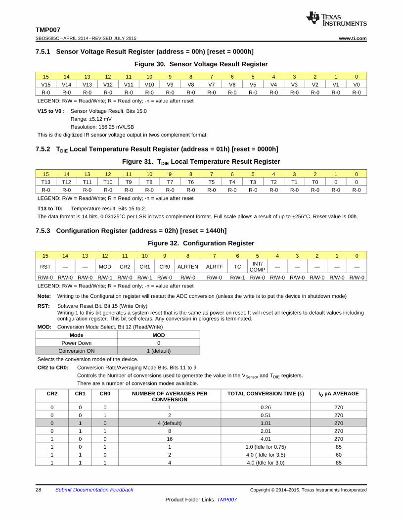
7.5.1 Sensor Voltage Result Register (address = 00h) [reset = 0000h]
Figure 30. Sensor Voltage Result Register
15 14 13 12 11 10 9 8 7 6 5 4 3 2 1 0V15 V14 V13 V12 V11 V10 V9 V8 V7 V6 V5 V4 V3 V2 V1 V0R-0 R-0 R-0 R-0 R-0 R-0 R-0 R-0 R-0 R-0 R-0 R-0 R-0 R-0 R-0 R-0
LEGEND: R/W = Read/Write; R = Read only; -n = value after reset
V15 to V0 : Sensor Voltage Result. Bits 15:0Range: ±5.12 mVResolution: 156.25 nV/LSB
This is the digitized IR sensor voltage output in twos complement format.
7.5.2 TDIE Local Temperature Result Register (address = 01h) [reset = 0000h]
Figure 31. TDIE Local Temperature Result Register
15 14 13 12 11 10 9 8 7 6 5 4 3 2 1 0T13 T12 T11 T10 T9 T8 T7 T6 T5 T4 T3 T2 T1 T0 0 0R-0 R-0 R-0 R-0 R-0 R-0 R-0 R-0 R-0 R-0 R-0 R-0 R-0 R-0 R-0 R-0
LEGEND: R/W = Read/Write; R = Read only; -n = value after reset
T13 to T0: Temperature result. Bits 15 to 2.The data format is 14 bits, 0.03125°C per LSB in twos complement format. Full scale allows a result of up to ±256°C. Reset value is 00h.
7.5.3 Configuration Register (address = 02h) [reset = 1440h]
Figure 32. Configuration Register
15 14 13 12 11 10 9 8 7 6 5 4 3 2 1 0
RST — — MOD CR2 CR1 CR0 ALRTEN ALRTF TC INT/COMP — — — — —
R/W-0 R/W-0 R/W-0 R/W-1 R/W-0 R/W-1 R/W-0 R/W-0 R/W-0 R/W-1 R/W-0 R/W-0 R/W-0 R/W-0 R/W-0 R/W-0LEGEND: R/W = Read/Write; R = Read only; -n = value after reset
Note: Writing to the Configuration register will restart the ADC conversion (unless the write is to put the device in shutdown mode)
RST: Software Reset Bit. Bit 15 (Write Only)Writing 1 to this bit generates a system reset that is the same as power on reset. It will reset all registers to default values includingconfiguration register. This bit self-clears. Any conversion in progress is terminated.
MOD: Conversion Mode Select, Bit 12 (Read/Write)Mode MOD
Power Down 0Conversion ON 1 (default)
Selects the conversion mode of the device.CR2 to CR0: Conversion Rate/Averaging Mode Bits. Bits 11 to 9
Controls the Number of conversions used to generate the value in the VSensor and TDIE registers.There are a number of conversion modes available.
CR2 CR1 CR0 NUMBER OF AVERAGES PERCONVERSION
TOTAL CONVERSION TIME (s) IQ µA AVERAGE
0 0 0 1 0.26 2700 0 1 2 0.51 2700 1 0 4 (default) 1.01 2700 1 1 8 2.01 2701 0 0 16 4.01 2701 0 1 1 1.0 (Idle for 0.75) 851 1 0 2 4.0 ( Idle for 3.5) 601 1 1 4 4.0 (Idle for 3.0) 85

29
TMP007www.ti.com SBOS685C –APRIL 2014–REVISED JULY 2015
Product Folder Links: TMP007
Submit Documentation FeedbackCopyright © 2014–2015, Texas Instruments Incorporated
ALRTEN: Alert Pin Enable. Bit 8Makes ALERT pin controlled by the alert flag bit. The ALERT pin is active low. The ALRTEN bit is mirrored in the status maskand enable register. Writing to the ALRTEN bit in the status mask and enable register also sets this bit, and vice versa.
ALRTF: Cumulative Alert Flag. Bit 7 (Read Only)This flag is the logical OR of all enabled flags, and is cleared when the status register is read in INT mode or at the end of aconversion when all enabled flags are 0 in COMP mode.It is mirrored in Status register.
TC: Transient Correction Enable. Bit 6Setting this bit turns on the transient correction enabling sensor voltage and object temperature output filtering.
INT/COMP: INT/COMP Mode. Bit 5The INT/COMP bit controls whether the limit flags are in INTERRUPT (INT) Mode (0) or COMPARATOR (COMP) Mode (1).It controls the behavior of the limit flags (LH, LL, OH, OL) and the data invalid flag (nDVF) from the status register.
7.5.4 TOBJ Object Temperature Result Register (address = 03h) [reset = 0000h]
Figure 33. TOBJ Object Temperature Result Register
15 14 13 12 11 10 9 8 7 6 5 4 3 2 1 0T13 T12 T11 T10 T9 T8 T7 T6 T5 T4 T3 T2 T1 T0 — nDVR-0 R-0 R-0 R-0 R-0 R-0 R-0 R-0 R-0 R-0 R-0 R-0 R-0 R-0 R-0 R-0
LEGEND: R/W = Read/Write; R = Read only; -n = value after reset
T13 to T0: Temperature result. Bits 15 to 2The data format is twos complement, 14 bits, and 0.03125°C per LSB. Full scale allows a result of up to ±256°C. Resetvalue is 00h.
nDV: Data invalid bit. Bit 0If this bit is set, it indicates that the calculated object temperature is not valid due to invalid operations in the math engine.The bit is reset in the next valid conversion.
7.5.5 Status Register (address = 04h) [reset = 0000h]The status register flags are activated whenever their limit is violated, and latch if the INT/COMP bit is in INTmode (see configuration register). In INT mode these flags are cleared only when the status register is read. Ifthe flag is set from a previous conversion, and at the end of the next conversion, the corresponding limit is notviolating anymore, the flag is not cleared when in INT mode. In COMP mode, these flags are set whenever thecorresponding limit is violated at the end of a conversion, and cleared if they are not.
Figure 34. Status Register
15 14 13 12 11 10 9 8 7 6 5 4 3 2 1 0ALRTF CRTF OHF OLF LHF LLF nVDF MCRPT SNRL — — — — — — —
R-0 R-0 R-0 R-0 R-0 R-0 R-0 R-0 R-0 R-0 R-0 R-0 R-0 R-0 R-0 R-0LEGEND: R/W = Read/Write; R = Read only; -n = value after reset
ALRTF: Cumulative Alert Flag Bit. Bit 15This flag is the logical OR of all enabled flags, and is cleared when the status register is read in INT mode or at the end of aconversion when all enabled flags are 0 in COMP mode.
CRTF: Conversion Ready Flag. Bit 14The conversion ready flag is provided to help coordinate one-shot conversions for temperature measurements. The bit is setafter the local and object temperature conversions have completed and the results are ready to be read in the result registers.This flag can be cleared by reading the status register, writing to the configuration register or reading any of the results registers(TDIE, TOBJ, and so on). This flag is not affected by the INT/COMP bit setting and is always in latched mode.
OHF: Object Temperature High Limit Flag. Bit 13This bit is set to 1 if the result in the object temperature register exceeds the value in the object temperature high limit register.In INT mode, this bit is cleared when the status register is read.
OLF: Object Temperature Low Limit Flag. Bit 12This bit is set to 1 if the result in the object temperature register is less than the value in the object temperature low limit register.In INT mode, this bit is cleared when the status register is read. In COMP mode, this bit is disabled and always reads 0.
LHF: Local Temperature (TDIE) High Limit Flag. Bit 11This bit is set to 1 if the result in the TDIE local temperature result register exceeds the value in the local temperature high limitregister. In COMP mode, the bit is cleared to 0 when the result in the TDIE local temperature result register is less than theobject temperature low limit. In INT mode, the bit is cleared when the status register is read.

30
TMP007SBOS685C –APRIL 2014–REVISED JULY 2015 www.ti.com
Product Folder Links: TMP007
Submit Documentation Feedback Copyright © 2014–2015, Texas Instruments Incorporated
LLF: Local Temperature (TDIE) Low Limit Flag. Bit 10This bit is set to 1 if the result in the TDIE local temperature result register goes below the value in the local temperature low limitregister. In INT mode, the bit is cleared when the status register is read. In COMP mode, the bit is disabled and always reads 0.
nDVF: Data Invalid Flag. Bit 9If the calculated object temperature is invalid due to an internal error in the math engine or if sensor voltage is out of range, thenData invalid flag is set. In INT mode, this flag can only be cleared by reading the status register. In COMP mode it is cleared atthe end of the conversion if the calculated object temperature and sensor voltage are valid.
MCRPT: Memory Corrupt Flag. Bit 8.This flag indicates an internal check on the memory failed. This check is automatically performed only on a general load of theregisters from memory that is done right after a power on reset, general call reset, or software reset (RST bit in the configurationregister), or by forcing loads through the memory access register. When this bit is set, it can only be cleared by a clean pass ofthe internal check on memory.Mirror of this bit is in memory access register, bit 12.
DOF: IR Data Overflow DATA_OVF Flag: Bit 7.This flag indicates if sensor voltage measured is over range. Combined with the data invalid bit, it tells why data is invalid.
Bits 6 to 0: Not used. These bits always read 0.
7.5.6 Status Mask and Enable Register (address = 05h) [reset = 0000h]
Figure 35. Status Mask and Enable Register
15 14 13 12 11 10 9 8 7 6 5 4 3 2 1 0
ALRTEN CRTEN OHEN OLEN LHEN LLEN DVEN MEM_C_EN — — — — — — — —
R/W-0 R/W-0 R/W-0 R/W-0 R/W-0 R/W-0 R/W-0 R/W-0 R/W-0 R/W-0 R/W-0 R/W-0 R/W-0 R/W-0 R/W-0 R/W-0LEGEND: R/W = Read/Write; R = Read only; -n = value after reset
ALRTEN: Alert Flag Enable Bit. Bit 150: ALRTF flag in status register cannot activate ALERT pin.1: ALRTF flag any enabled flag in Status register will activate ALERT pin.Can also be set by its mirror in Configuration register, bit 8.
CRTEN: Temperature Conversion Ready Enable Bit. Bit 140: CRTF flag in status register cannot activate ALRTF1: CRTF flag in Status register will activate ALRTF.
OHEN: Object Temperature High Limit Enable Bit. Bit 130: OHF flag in Status register cannot activate ALRTF.1: OHF flag in Status register will activate ALRTF.
OLEN: Object Temperature Low Limit Enable Bit. Bit 12INT Mode:0: OLF flag in Status register cannot activate ALRTF.1: OLF flag in Status register will activate ALRTF.COMP Mode: This bit is disabled in COMP mode and will always read 0.
LHEN: TDIE Temperature High Limit Enable Bit. Bit 110: AHF flag in Status register cannot activate ALRTF.1: AHF flag in Status register will activate ALRTF in INT mode
LLEN: TDIE Temperature Low Limit Enable Bit. Bit 10INT Mode (Alert Mode):0: ALF flag in Status register cannot activate ALRTF.1: ALF flag in Status register will activate ALRTF in INT modeCOMP Mode: This bit is disabled in COMP mode and always read 0.
DVEN: Data invalid Flag Enable Bit. Bit 90: Data invalid Flag in Status register cannot activate ALRTF.1: Data invalid Flag in Status register will activate ALRTF.
MEM_C_EN: Memory Corrupt Enable Bit. Bit 80: Memory Corrupt flag in Status register cannot activate ALRTF.1: Memory Corrupt flag in Status register will activate ALRTF.
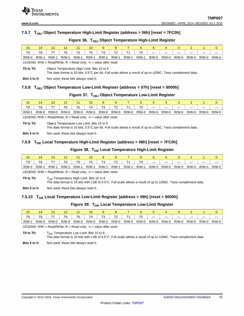
31
TMP007www.ti.com SBOS685C –APRIL 2014–REVISED JULY 2015
Product Folder Links: TMP007
Submit Documentation FeedbackCopyright © 2014–2015, Texas Instruments Incorporated
7.5.7 TOBJ Object Temperature High-Limit Register (address = 06h) [reset = 7FC0h]
Figure 36. TOBJ Object Temperature High-Limit Register
15 14 13 12 11 10 9 8 7 6 5 4 3 2 1 0T9 T8 T7 T6 T5 T4 T3 T2 T1 T0 — — — — — —
R/W-0 R/W-1 R/W-1 R/W-1 R/W-1 R/W-1 R/W-1 R/W-1 R/W-1 R/W-1 R/W-0 R/W-0 R/W-0 R/W-0 R/W-0 R/W-0LEGEND: R/W = Read/Write; R = Read only; -n = value after reset
T9 to T0: Object Temperature High Limit. Bits 15 to 6The data format is 10 bits, 0.5°C per bit. Full scale allows a result of up to ±256C. Twos complement data.
Bits 5 to 0: Not used; these bits always read 0.
7.5.8 TOBJ Object Temperature Low-Limit Register (address = 07h) [reset = 8000h]
Figure 37. TOBJ Object Temperature Low-Limit Register
15 14 13 12 11 10 9 8 7 6 5 4 3 2 1 0T9 T8 T7 T6 T5 T4 T3 T2 T1 T0 — — — — — —
R/W-1 R/W-0 R/W-0 R/W-0 R/W-0 R/W-0 R/W-0 R/W-0 R/W-0 R/W-0 R/W-0 R/W-0 R/W-0 R/W-0 R/W-0 R/W-0LEGEND: R/W = Read/Write; R = Read only; -n = value after reset
T9 to T0: Object Temperature Low Limit. Bits 15 to 6The data format is 10 bits, 0.5°C per bit. Full scale allows a result of up to ±256C. Twos complement data.
Bits 5 to 0: Not used; these bits always read 0.
7.5.9 TDIE Local Temperature High-Limit Register (address = 08h) [reset = 7FC0h]
Figure 38. TDIE Local Temperature High-Limit Register
15 14 13 12 11 10 9 8 7 6 5 4 3 2 1 0T9 T8 T7 T6 T5 T4 T3 T2 T1 T0 — — — — — —
R/W-0 R/W-1 R/W-1 R/W-1 R/W-1 R/W-1 R/W-1 R/W-1 R/W-1 R/W-1 R/W-0 R/W-0 R/W-0 R/W-0 R/W-0 R/W-0LEGEND: R/W = Read/Write; R = Read only; -n = value after reset
T9 to T0: TDIE Temperature High Limit. Bits 15 to 6The data format is 10 bits with LSB of 0.5°C. Full scale allows a result of up to ±256C. Twos complement data.
Bits 5 to 0: Not used; these bits always read 0.
7.5.10 TDIE Local Temperature Low-Limit Register (address = 09h) [reset = 8000h]
Figure 39. TDIE Local Temperature Low-Limit Register
15 14 13 12 11 10 9 8 7 6 5 4 3 2 1 0T9 T8 T7 T6 T5 T4 T3 T2 T1 T0 — — — — — —
R/W-1 R/W-0 R/W-0 R/W-0 R/W-0 R/W-0 R/W-0 R/W-0 R/W-0 R/W-0 R/W-0 R/W-0 R/W-0 R/W-0 R/W-0 R/W-0LEGEND: R/W = Read/Write; R = Read only; -n = value after reset
T9 to T0: TDIE Temperature Low Limit. Bits 15 to 6.The data format is 10 bits with LSB of 0.5°C. Full scale allows a result of up to ±256C. Twos complement data.
Bits 5 to 0: Not used; these bits always read 0.

32
TMP007SBOS685C –APRIL 2014–REVISED JULY 2015 www.ti.com
Product Folder Links: TMP007
Submit Documentation Feedback Copyright © 2014–2015, Texas Instruments Incorporated
(1) All signed values are twos complement data.
7.5.11 Coefficient RegistersThe values of the coefficient registers described above are used in the math engine. The range and resolution ofthe coefficients are shown in Table 9. The default coefficients, TC0 and TC1, are optimized for the defaultconversion mode (four averages per measurement). Different acquisition modes may require different values forthe TC0 and TC1 coefficients.
Table 9. Coefficient Range and Resolution (1)
REGISTERADDRESS VARIABLE BITS RANGE RESOLUTION DEFAULT VALUES
HEX DEFAULTVALUES
0A S0 16 0 – 298E-15 LSB = 4.5475E-18 4.430E-14 0260Eh0B A1 16 ±125E-3 LSB = 3.8150E-06 9.995E-04 0106h0C A2 16 ±1.9E-3 LSB = 5.9600E-08 –6.020E-06 FF9Bh0D B0 16 ±5.12E-3 LSB = 1.5625E-07 –3.094E-05 FF3Ah0E B1 16 ±20E-6 LSB = 6.1035E-10 –8.728E-08 FF71h0F B2 16 ±312E-9 LSB = 9.5367E-12 1.300E-08 0553h10 C2 12 ±97.65 LSB = 4.7680E-02 0 0000h11 TC0 16 ±163E-3 LSB = 5.0000E-06 2.600E-04 0034h12 TC1 16 ±1024 LSB = 3.1250E-02 0 0000h
7.5.11.1 S0 Coefficient Register (address = 0Ah) [reset = 260Eh]
Figure 40. S0 Coefficient Register
15 14 13 12 11 10 9 8 7 6 5 4 3 2 1 0S0_15 S0_14 S0_13 S0_12 S0_11 S0_10 S0_9 S0_8 S0_7 S0_6 S0_5 S0_4 S0_3 S0_2 S0_1 S0_0R/W-0 R/W-0 R/W-1 R/W-0 R/W-0 R/W-1 R/W-1 R/W-0 R/W-0 R/W-0 R/W-0 R/W-0 R/W-1 R/W-1 R/W-1 R/W-0LEGEND: R/W = Read/Write; R = Read only; -n = value after reset
S0_15 to S0_0: S0 Coefficient Value. Bits 15 to 0.Range and resolution given in Table 9
7.5.11.2 A1 Coefficient Register (address = 0Bh) [reset = 0106h]
Figure 41. A1 Coefficient Register
15 14 13 12 11 10 9 8 7 6 5 4 3 2 1 0A1_15 A1_14 A1_13 A1_12 A1_11 A1_10 A1_9 A1_8 A1_7 A1_6 A1_5 A1_4 A1_3 A1_2 A1_1 A1_0R/W-0 R/W-0 R/W-0 R/W-0 R/W-0 R/W-0 R/W-0 R/W-1 R/W-0 R/W-0 R/W-0 R/W-0 R/W-0 R/W-1 R/W-1 R/W-0LEGEND: R/W = Read/Write; R = Read only; -n = value after reset
A1_15 to A1_0: A1 Coefficient Value. Bits 15 to 0.Twos complement format. Range and resolution given in Table 9
7.5.11.3 A2 Coefficient Register (address = 0Ch) [reset = FF9Bh]
Figure 42. A2 Coefficient Register
15 14 13 12 11 10 9 8 7 6 5 4 3 2 1 0A2_15 A2_14 A2_13 A2_12 A2_11 A2_10 A2_9 A2_8 A2_7 A2_6 A2_5 A2_4 A2_3 A2_2 A2_1 A2_0R/W-1 R/W-1 R/W-1 R/W-1 R/W-1 R/W-1 R/W-1 R/W-1 R/W-1 R/W-0 R/W-0 R/W-1 R/W-1 R/W-0 R/W-1 R/W-1LEGEND: R/W = Read/Write; R = Read only; -n = value after reset
A2_15 to A2_0: A2 Coefficient Value. Bits 15 to 0Twos complement format. Range and resolution given in Table 9

33
TMP007www.ti.com SBOS685C –APRIL 2014–REVISED JULY 2015
Product Folder Links: TMP007
Submit Documentation FeedbackCopyright © 2014–2015, Texas Instruments Incorporated
7.5.11.4 B0 Coefficient Register (address = 0Dh) [reset = FF3Ah]
Figure 43. B0 Coefficient Register
15 14 13 12 11 10 9 8 7 6 5 4 3 2 1 0B0_15 B0_14 B0_13 B0_12 B0_11 B0_10 B0_9 B0_8 B0_7 B0_6 B0_5 B0_4 B0_3 B0_2 B0_1 B0_0R/W-1 R/W-1 R/W-1 R/W-1 R/W-1 R/W-1 R/W-1 R/W-1 R/W-0 R/W-0 R/W-1 R/W-1 R/W-1 R/W-0 R/W-1 R/W-0LEGEND: R/W = Read/Write; R = Read only; -n = value after reset
B0_15 to B0_0: B0 Coefficient Value. Bits 15 to 0Twos complement format. Range and resolution given in Table 9
7.5.11.5 B1 Coefficient Register (address = 0Eh) [reset = FF71h]
Figure 44. B1 Coefficient Register
15 14 13 12 11 10 9 8 7 6 5 4 3 2 1 0B1_15 B1_14 B1_13 B1_12 B1_11 B1_10 B1_9 B1_8 B1_7 B1_6 B1_5 B1_4 B1_3 B1_2 B1_1 B1_0R/W-1 R/W-1 R/W-1 R/W-1 R/W-1 R/W-1 R/W-1 R/W-1 R/W-0 R/W-1 R/W-1 R/W-1 R/W-0 R/W-0 R/W-0 R/W-1LEGEND: R/W = Read/Write; R = Read only; -n = value after reset
B1_15 to B1_0: B1 Coefficient Value. Bits 15 to 0Twos complement format. Range and resolution given in Table 9
7.5.11.6 B2 Coefficient Register (address = 0Fh) [reset = 0553h]
Figure 45. B2 Coefficient Register
15 14 13 12 11 10 9 8 7 6 5 4 3 2 1 0B2_15 B2_14 B2_13 B2_12 B2_11 B2_10 B2_9 B2_8 B2_7 B2_6 B2_5 B2_4 B2_3 B2_2 B2_1 B2_0R/W-0 R/W-0 R/W-0 R/W-0 R/W-0 R/W-1 R/W-0 R/W-1 R/W-0 R/W-1 R/W-0 R/W-1 R/W-0 R/W-0 R/W-1 R/W-1LEGEND: R/W = Read/Write; R = Read only; -n = value after reset
B2_15 to B2_0: B2 Coefficient Value. Bits 15 to 0Twos complement format. Range and resolution given in Table 9
7.5.11.7 C2 Coefficient Register (address = 10h) [reset = 0000h]
Figure 46. C2 Coefficient Register
15 14 13 12 11 10 9 8 7 6 5 4 3 2 1 0C2_11 C2_10 C2_9 C2_8 C2_7 C2_6 C2_5 C2_4 C2_3 C2_2 C2_1 C2_0 — — — —R/W-0 R/W-0 R/W-0 R/W-0 R/W-0 R/W-0 R/W-0 R/W-0 R/W-0 R/W-0 R/W-0 R/W-0 R/W-0 R/W-0 R/W-0 R/W-0LEGEND: R/W = Read/Write; R = Read only; -n = value after reset
C2_11 to C2_0: C2 Coefficient Value. Bits 15 to 4Twos complement format. Range and resolution given in Table 9
7.5.11.8 TC0 Coefficient Register (address = 11h) [reset = 0034h]
Figure 47. TC0 Coefficient Register
15 14 13 12 11 10 9 8 7 6 5 4 3 2 1 0TC0_
15TC0_
14TC0_
13TC0_
12TC0_
11TC0_
10 TC0_9 TC0_8 TC0_7 TC0_6 TC0_5 TC0_4 TC0_3 TC0_2 TC0_1 TC0_0
R/W-0 R/W-0 R/W-0 R/W-0 R/W-0 R/W-0 R/W-0 R/W-0 R/W-0 R/W-0 R/W-1 R/W-1 R/W-0 R/W-1 R/W-0 R/W-0LEGEND: R/W = Read/Write; R = Read only; -n = value after reset
TC0_15 to TC0_0: TC0 Coefficient Value. Bits 15 to 0Twos complement format. Range and resolution given in Table 9

34
TMP007SBOS685C –APRIL 2014–REVISED JULY 2015 www.ti.com
Product Folder Links: TMP007
Submit Documentation Feedback Copyright © 2014–2015, Texas Instruments Incorporated
7.5.11.9 TC1 Coefficient Register (address = 12h) [reset = 0000h]
Figure 48. TC1 Coefficient Register
15 14 13 12 11 10 9 8 7 6 5 4 3 2 1 0TC1_
15TC1_
14TC1_
13TC1_
12TC1_
11TC1_
10 TC1_9 TC1_8 TC1_7 TC1_6 TC1_5 TC1_4 TC1_3 TC1_2 TC1_1 TC1_0
R/W-0 R/W-0 R/W-0 R/W-0 R/W-0 R/W-0 R/W-0 R/W-0 R/W-0 R/W-0 R/W-0 R/W-0 R/W-0 R/W-0 R/W-0 R/W-0LEGEND: R/W = Read/Write; R = Read only; -n = value after reset
TC1_15 to TC1_0: TC1 Coefficient Value. Bits 15 to 0Twos complement format. Range and resolution given in Table 9
7.5.12 Manufacturer ID Register (address = 1Eh) [reset = 5449h]
Figure 49. Manufacturer ID Register
15 14 13 12 11 10 9 8 7 6 5 4 3 2 1 0ID15 ID14 ID13 ID12 ID11 ID10 ID9 ID8 ID7 ID6 ID5 ID4 ID3 ID2 ID1 ID0R-0 R-1 R-0 R-1 R-0 R-1 R-0 R-0 R-0 R-1 R-0 R-0 R-1 R-0 R-0 R-1
LEGEND: R/W = Read/Write; R = Read only; -n = value after reset
ID15 to ID0: Manufacturer ID Bits. Bits 15 to 0. Reads 'TI' in ASCII code.
7.5.13 Device ID Register (address = 1Fh) [reset = 0078h]
Figure 50. Device ID Register
15 14 13 12 11 10 9 8 7 6 5 4 3 2 1 0DID11 DID10 DID9 DID8 DID7 DID6 DID5 DID4 DID3 DID2 DID1 DID0 RID3 RID2 RID1 RID0
R-0 R-0 R-0 R-0 R-0 R-0 R-0 R-0 R-0 R-1 R-1 R-1 R-1 R-0 R-0 R-0LEGEND: R/W = Read/Write; R = Read only; -n = value after reset
DID11 to DID0: Device ID Bits. Bits 15 to 4. Reads 007h.RID3 to RID0: Revision ID Bits. Bits 3 to 0. Reads 8h.

35
TMP007www.ti.com SBOS685C –APRIL 2014–REVISED JULY 2015
Product Folder Links: TMP007
Submit Documentation FeedbackCopyright © 2014–2015, Texas Instruments Incorporated
7.5.14 Memory Access Register (address = 2Ah) [reset = 0000h]The internal memory can be accessed through the memory access register. When the register is read, it returnsthe values in read name. When the register is written to, it must contain the value 6Axxh to enable the contentsof the register specified by Adr4 to Adr0 to be stored in memory.
Figure 51. Memory Access Register: Read
15 14 13 12 11 10 9 8 7 6 5 4 3 2 1 0
nwR_2 nwR_1 nwR_0 MemCrpt — — — — Adr4 Adr3 Adr2 Adr1 Adr0 0 0 0
R/W-0 R/W-0 R/W-0 R/W-0 R/W-0 R/W-0 R/W-0 R/W-0 R/W-0 R/W-0 R/W-0 R/W-0 R/W-0 R/W-0 R/W-0 R/W-0LEGEND: R/W = Read/Write; R = Read only; -n = value after reset
Figure 52. Memory Access Register: Write
15 14 13 12 11 10 9 8 7 6 5 4 3 2 1 0
0 1 1 0 1 0 1 0 Adr4 Adr3 Adr2 Adr1 Adr0Gener
alLoad
MemStore
SingleLoad
N/A N/A N/A N/A N/A N/A N/A N/A N/A N/A N/A N/A N/A N/A N/A N/ALEGEND: N/A = reset value not applicable for write operation.
nwR_2 to nwR_0: Number of Programs. Bits 15 to 13.A memory location can be programmed a maximum of eight times. These bits contain the number of times thislocation has been programmed. After the eighth programming to a given location, subsequent attempts to programare ignored.
Mem Crpt: Memory Corrupt. Bit 12 (read only).This bit is a mirror of bit 8 in the status register.
Adr4 to Adr0: Memory Address. Bits 7 to 3.Used to specify register address to operate on. Address here is the same as the register in register address table..
General Load: General Load. Bit 2 (write only).Loads all registers from memory with the last value stored in memory for that register. Adr[4:0] are don’t care in thiscase.
Mem Store: Memory Store. Bit 1 (write only).Write 1 to this bit along with the register address to store that registers contents to memory.
Single Load: Single Load. Bit 0.Performs an load of the memory contents to the register address determined by the Adr[4:0] bits.
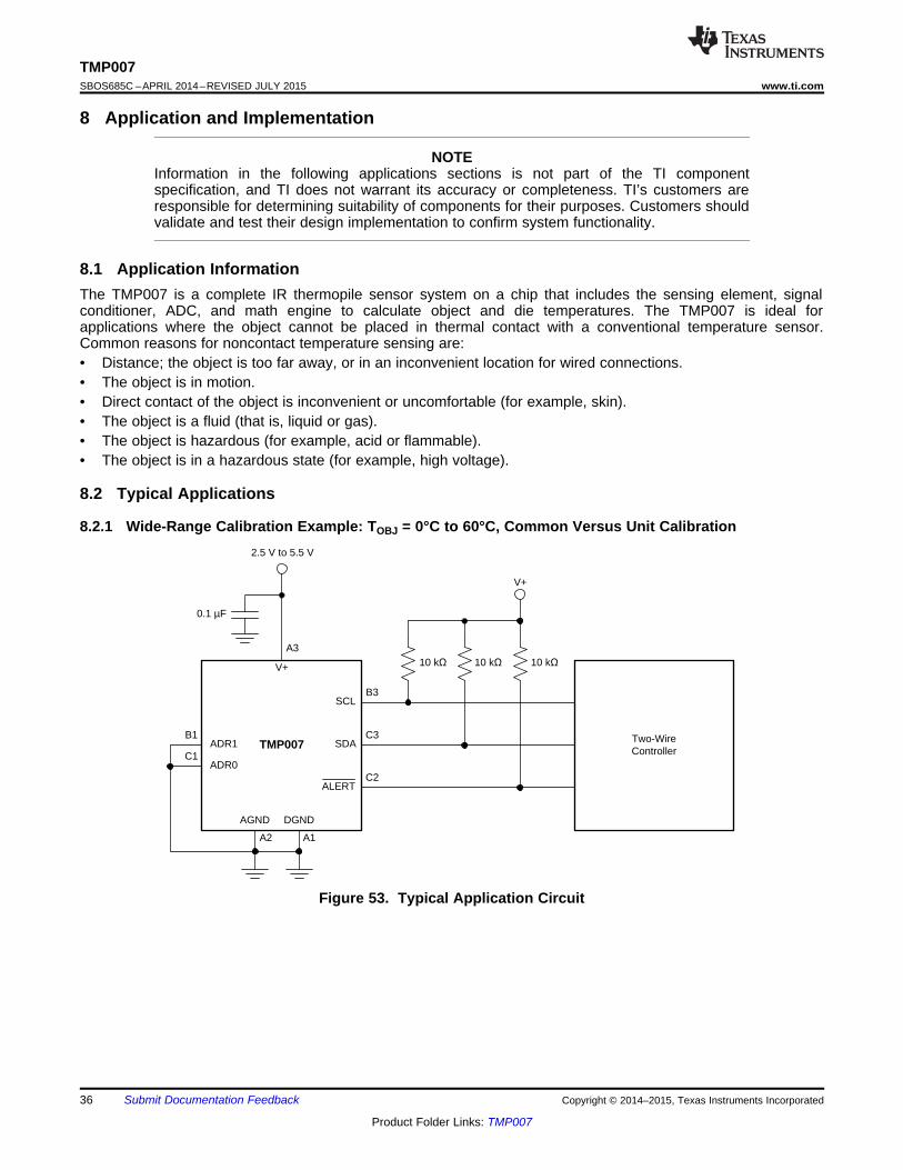
ADR1
SCL
SDA
AGND
V+
ALERT
Two-Wire Controller
A3
B1
C2
B3
C3
A2
TMP007
2.5 V to 5.5 V
0.1 µF
ADR0C1
DGND
A1
10 k 10 k 10 k
V+
36
TMP007SBOS685C –APRIL 2014–REVISED JULY 2015 www.ti.com
Product Folder Links: TMP007
Submit Documentation Feedback Copyright © 2014–2015, Texas Instruments Incorporated
8 Application and Implementation
NOTEInformation in the following applications sections is not part of the TI componentspecification, and TI does not warrant its accuracy or completeness. TI’s customers areresponsible for determining suitability of components for their purposes. Customers shouldvalidate and test their design implementation to confirm system functionality.
8.1 Application InformationThe TMP007 is a complete IR thermopile sensor system on a chip that includes the sensing element, signalconditioner, ADC, and math engine to calculate object and die temperatures. The TMP007 is ideal forapplications where the object cannot be placed in thermal contact with a conventional temperature sensor.Common reasons for noncontact temperature sensing are:• Distance; the object is too far away, or in an inconvenient location for wired connections.• The object is in motion.• Direct contact of the object is inconvenient or uncomfortable (for example, skin).• The object is a fluid (that is, liquid or gas).• The object is hazardous (for example, acid or flammable).• The object is in a hazardous state (for example, high voltage).
8.2 Typical Applications
8.2.1 Wide-Range Calibration Example: TOBJ = 0°C to 60°C, Common Versus Unit Calibration
Figure 53. Typical Application Circuit

37
TMP007www.ti.com SBOS685C –APRIL 2014–REVISED JULY 2015
Product Folder Links: TMP007
Submit Documentation FeedbackCopyright © 2014–2015, Texas Instruments Incorporated
Typical Applications (continued)8.2.1.1 Design RequirementsFor this application, the system must operate over the environment described in Table 10.
Table 10. Wide-Range ParametersDESIGN PARAMETER EXAMPLE VALUE COMMENT
N 32 Number of devices in calibration setMinimum TDIE 0°C Minimum expected die temperatureMaximum TDIE 60°C Maximum expected die temperatureMinimum TOBJ 0°C Minimum expected objected temperatureMaximum TOBJ 60°C Maximum expected object temperature
ε 0.95 Object emissivityField of view 110° Field of view subtended by object
Conversion rate 1 sample/second
Select a set of values for TDIE and TOBJ to generate the calibration set. At a minimum, include the four extremepoints of the temperature ranges desired. In practice, it is best to include a number of intermediate points as well.This example uses the values shown in Table 11, with an X marking the values chosen for measurement.
Table 11. Wide-Range Measurement Values
TOBJ
TDIE
0°C 20°C 40°C 60°C0°C X X X X20°C X X X X40°C X X X X60°C X X X X

( )NORM MEASSensor (mV) Sensor a SampleNo b= - ´ +
Sensor (mV) a SampleNo b= ´ +
38
TMP007SBOS685C –APRIL 2014–REVISED JULY 2015 www.ti.com
Product Folder Links: TMP007
Submit Documentation Feedback Copyright © 2014–2015, Texas Instruments Incorporated
8.2.1.2 Detailed Design ProcedureBefore attempting to calibrate the system, it is necessary to establish the stability of the system. Noise is ameasure of precision, which is the random deviation from the mean of the distribution. For a Gaussian (ornormal) distribution, the precision is typically characterized by the standard deviation (sensor noise), σ.
8.2.1.2.1 Wide-Range Calibration
To begin calibration, select an object temperature (TOBJ) and a value for the die temperature (TDIE). With thesesystem temperatures stable, take a statistically significant number of samples of VSensor (results shown in register00h).
in this example, 64 samples were taken. Do not use the object temperature readings given in register 03h; thesevalues are invalid before calibration.
To compensate for first order drift in system temperatures, it is often useful to normalize the data set. For thispurpose, for each temperature set, the sensor voltage data (given in register 00h) is normalized by first findingthe best fit line of the form shown in Equation 11:
(11)
The normalized data for each data set is then calculated as shown in Equation 12:(12)
The normalized data, VSensor_norm, is centered on zero mean, and is first-order corrected for long-term drift. Thestandard deviation for each data set is then calculated to estimate the sensor noise, σ. Verify that the data arelimited by white noise and no other effects. For a sensor-noise-limited data set, vSENSOR σ is typically < 1 μV, andpreferably < 0.5 μV after first-order correction for drift, as described previously. If this condition is not satisfied,then the calibration accuracy is limited by external system factors (for example, convection or conduction).Repeat this process for each combination of TOBJ and TDIE for which the calibration is to be performed. Thenormalized data are used only for evaluating the suitability of the data set for calibration, and not for the actualcalibration itself.
For calibration, the mean value, <VSENSOR>, is calculated for each combination of TOBJ and TDIE, as shown inTable 12. Using the mean value minimizes error introduced by random noise. Based on the means, a set ofcoefficients is generated based on a user-selected optimization criteria for Equation 7. Common criteria areminimizing the maximum error, minimizing the average error, and so on. For a detailed discussion of optimizationmethods, see SBOU142 — TMP007 Calibration Guide.
Table 12. Mean Values
TOBJ
TDIE
0°C 20°C 40°C 60°C0°C <VSENSOR> <VSENSOR> <VSENSOR> <VSENSOR>20°C <VSENSOR> <VSENSOR> <VSENSOR> <VSENSOR>40°C <VSENSOR> <VSENSOR> <VSENSOR> <VSENSOR>60°C <VSENSOR> <VSENSOR> <VSENSOR> <VSENSOR>
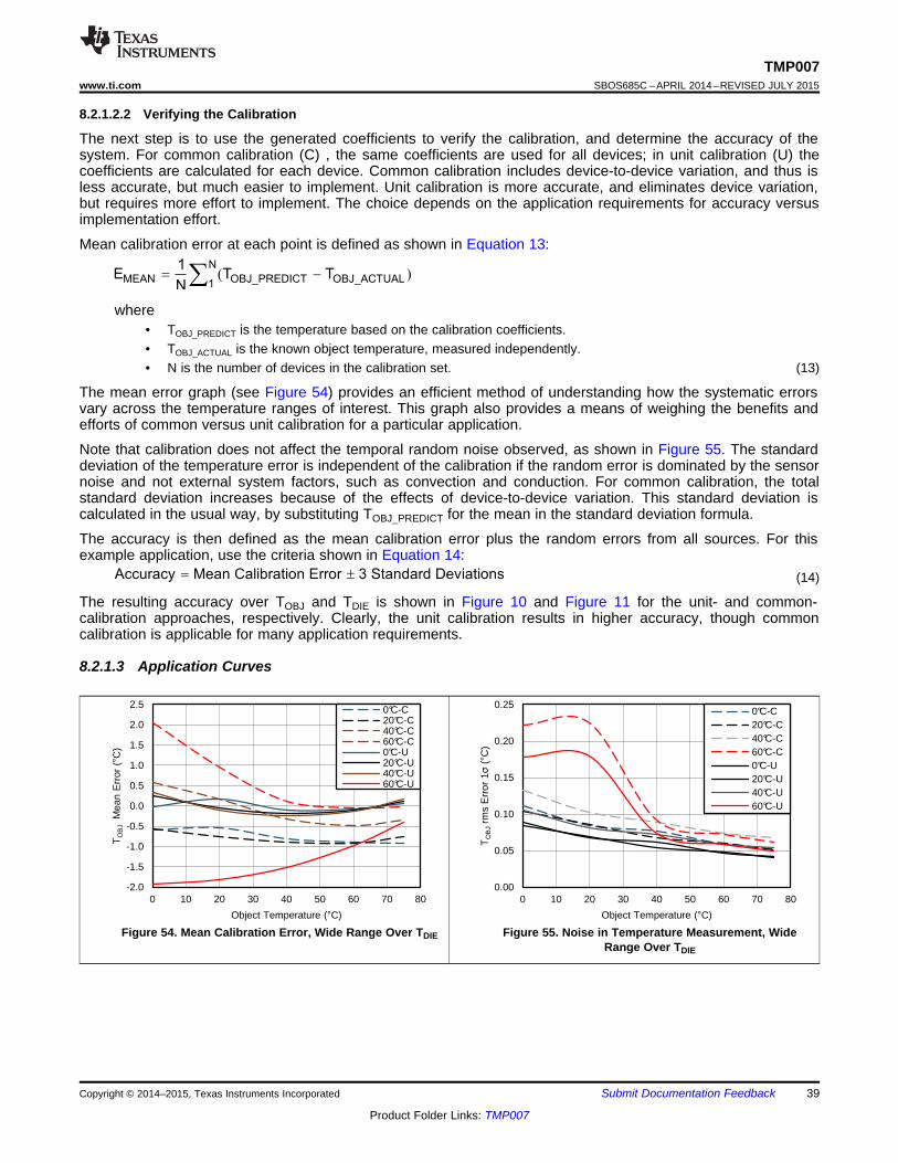
-2.0
-1.5
-1.0
-0.5
0.0
0.5
1.0
1.5
2.0
2.5
0 10 20 30 40 50 60 70 80
TO
BJ
Mea
n E
rror
(�C
)
Object Temperature (�C)
0°C-C20°C-C40°C-C60°C-C0°C-U20°C-U40°C-U60°C-U
C015
0.00
0.05
0.10
0.15
0.20
0.25
0 10 20 30 40 50 60 70 80
TO
BJ
rms
Err
or 11
(�C
)
Object Temperature (�C)
0°C-C20°C-C40°C-C60°C-C0°C-U20°C-U40°C-U60°C-U
C016
Accuracy Mean Calibration Error 3 Standard Deviations= ±
( )N
MEAN OBJ_PREDICT OBJ_ACTUAL1
1E T T
N= -å
39
TMP007www.ti.com SBOS685C –APRIL 2014–REVISED JULY 2015
Product Folder Links: TMP007
Submit Documentation FeedbackCopyright © 2014–2015, Texas Instruments Incorporated
8.2.1.2.2 Verifying the Calibration
The next step is to use the generated coefficients to verify the calibration, and determine the accuracy of thesystem. For common calibration (C) , the same coefficients are used for all devices; in unit calibration (U) thecoefficients are calculated for each device. Common calibration includes device-to-device variation, and thus isless accurate, but much easier to implement. Unit calibration is more accurate, and eliminates device variation,but requires more effort to implement. The choice depends on the application requirements for accuracy versusimplementation effort.
Mean calibration error at each point is defined as shown in Equation 13:
where• TOBJ_PREDICT is the temperature based on the calibration coefficients.• TOBJ_ACTUAL is the known object temperature, measured independently.• N is the number of devices in the calibration set. (13)
The mean error graph (see Figure 54) provides an efficient method of understanding how the systematic errorsvary across the temperature ranges of interest. This graph also provides a means of weighing the benefits andefforts of common versus unit calibration for a particular application.
Note that calibration does not affect the temporal random noise observed, as shown in Figure 55. The standarddeviation of the temperature error is independent of the calibration if the random error is dominated by the sensornoise and not external system factors, such as convection and conduction. For common calibration, the totalstandard deviation increases because of the effects of device-to-device variation. This standard deviation iscalculated in the usual way, by substituting TOBJ_PREDICT for the mean in the standard deviation formula.
The accuracy is then defined as the mean calibration error plus the random errors from all sources. For thisexample application, use the criteria shown in Equation 14:
(14)
The resulting accuracy over TOBJ and TDIE is shown in Figure 10 and Figure 11 for the unit- and common-calibration approaches, respectively. Clearly, the unit calibration results in higher accuracy, though commoncalibration is applicable for many application requirements.
8.2.1.3 Application Curves
Figure 54. Mean Calibration Error, Wide Range Over TDIE Figure 55. Noise in Temperature Measurement, WideRange Over TDIE

ADR1
SCL
SDA
AGND
V+
ALERT
Two-Wire Controller
A3
B1
C2
B3
C3
A2
TMP007
2.5 V to 5.5 V
0.1 µF
ADR0C1
DGND
A1
10 k 10 k 10 k
V+
40
TMP007SBOS685C –APRIL 2014–REVISED JULY 2015 www.ti.com
Product Folder Links: TMP007
Submit Documentation Feedback Copyright © 2014–2015, Texas Instruments Incorporated
8.2.2 Narrow-Range Calibration Example: TOBJ = 33°C to 41°C, Unit vs Common Calibration
Figure 56. Typical Application Circuit
8.2.2.1 Design RequirementsFor this application, the system must operate over the environment described in Table 13.
Table 13. Narrow-Range RequirementsDESIGN PARAMETER EXAMPLE VALUE COMMENT
N 16 Number of devices in calibration setMinimum TDIE 25°C Minimum expected die temperatureMaximum TDIE 30°C Maximum expected die temperatureMinimum TOBJ 33°C Minimum expected objected temperatureMaximum TOBJ 41°C Maximum expected object temperature
ε 0.95 Object emissivityField of view 110° Field of view subtended by object
Conversion rate 1 sample/second
Select a set of values for TDIE and TOBJ to generate the calibration set. At a minimum, include the four extremepoints of the temperature ranges desired. In practice, it is best to include a number of intermediate points as well.This example uses the values shown in Table 14, with an X marking the values chosen for measurement. In thisapplication, the calibration set is weighted more densely around the region of interest.
Table 14. Narrow-Range Measurement Values
TDIE
TOBJ
33°C 34°C 35°C 36°C 36.5°C 37°C 37.5°C 38°C 38.5°C 39°C 40°C 41°C25°C X X X X X X X X X X X X30°C X X X X X X
8.2.2.2 Detailed Design ProcedureBefore attempting to calibrate the system, it is necessary to establish the stability of the system. Noise is ameasure of precision, which is the random deviation from the mean of the distribution. For a Gaussian (ornormal) distribution, the precision is typically characterized by the standard deviation (sensor noise), σ.

( )N
MEAN OBJ_PREDICT OBJ_ACTUAL1
1E T T
N= -å
( )NORM MEASSensor (mV) Sensor a SampleNo b= - ´ +
Sensor (mV) a SampleNo b= ´ +
41
TMP007www.ti.com SBOS685C –APRIL 2014–REVISED JULY 2015
Product Folder Links: TMP007
Submit Documentation FeedbackCopyright © 2014–2015, Texas Instruments Incorporated
8.2.2.2.1 Narrow-Range Calibration
To begin calibration, select an object temperature (TOBJ) and a value for the die temperature (TDIE). With thesesystem temperatures stable, take a statistically significant number of samples of VSensor (results shown in register00h).
in this example, 64 samples were taken. Do not use the object temperature readings given in register 03h; thesevalues are invalid before calibration.
To compensate for first order drift in system temperatures, it is often useful to normalize the data set. For thispurpose, for each temperature set, the sensor voltage data (given in register 00h) is normalized by first findingthe best fit line of the form shown in Equation 15:
(15)
The normalized data for each data set is then calculated as shown in Equation 16:(16)
The normalized data, VSensor_norm, is centered on zero mean, and is first-order corrected for long-term drift. Thestandard deviation for each data set is then calculated to estimate the sensor noise, σ. Verify that the data arelimited by white noise and no other effects. For a sensor-noise-limited data set, vSENSOR σ is typically < 1 μV, andpreferably < 0.5 μV after first-order correction for drift, as described previously. If this condition is not satisfied,then the calibration accuracy is limited by external system factors (for example, convection or conduction).Repeat this process for each combination of TOBJ and TDIE for which the calibration is to be performed. Thenormalized data are used only for evaluating the suitability of the data set for calibration, and not for the actualcalibration itself.
For calibration, the mean value, <VSENSOR>, is calculated for each combination of TOBJ and TDIE, as shown inTable 15. Using the mean value minimizes error introduced by random noise. Based on the means, a set ofcoefficients is generated based on a user-selected optimization criteria for Equation 7. Common criteria areminimizing the maximum error, minimizing the average error, and so on. For a detailed discussion of optimizationmethods, see SBOU142 — TMP007 Calibration Guide.
Table 15. Mean Values
TDIE(°C)
TOBJ
33°C 34°C 35°C 36°C 36.5°C 37°C 37.5°C 38°C 38.5°C 39°C 40°C 41°C
25 <VSENSOR> <VSENSOR> <VSENSOR> <VSENSOR> <VSENSOR> <VSENSOR> <VSENSOR> <VSENSOR> <VSENSOR> <VSENSOR> <VSENSOR> <VSENSOR>
30 <VSENSOR> <VSENSOR> <VSENSOR> <VSENSOR> <VSENSOR> <VSENSOR>
8.2.2.2.2 Verifying the Calibration
The next step is to use the generated coefficients to verify the calibration, and determine the accuracy of thesystem. For common calibration (C) , the same coefficients are used for all devices; in unit calibration (U) thecoefficients are calculated for each device. Common calibration includes device-to-device variation, and thus isless accurate, but much easier to implement. Unit calibration is more accurate, and eliminates device variation,but requires more effort to implement. The choice depends on the application requirements for accuracy versusimplementation effort.
Mean calibration error at each point is defined as shown in Equation 17:
where• TOBJ_PREDICT is the temperature based on the calibration coefficients.• TOBJ_ACTUAL is the known object temperature, measured independently.• N is the number of devices in the calibration set. (17)
The mean error graph (see Figure 54) provides an efficient method of understanding how the systematic errorsvary across the temperature ranges of interest. This graph also provides a means of weighing the benefits andefforts of common versus unit calibration for a particular application.

-1.00
-0.75
-0.50
-0.25
0.00
0.25
0.50
0.75
1.00
30 32 34 36 38 40 42 44 46
TO
BJ
Acc
urac
y -
Uni
t Cal
ibra
tion
(�C
)
Object Temperature (�C)
25°C-1 s25°C-4 s30°C-1 s30°C-4 s
C017
-2.0
-1.5
-1.0
-0.5
0.0
0.5
1.0
1.5
2.0
30 32 34 36 38 40 42 44 46
TO
BJ
Acc
urac
y E
rror
(�C
)
Object Temperature (�C)
25°C-U25°C-C30°C-U30°C-C
C015
0.00
0.05
0.10
0.15
0.20
0.25
0.30
0.35
0.40
0.45
0.50
30 32 34 36 38 40 42 44 46
TO
BJ
rms
Err
or 11
(�C
)
Object Temperature (�C)
C-1 s
U-1 s
U-4 s
C016
Accuracy Mean Calibration Error 3 Standard Deviations= ±
42
TMP007SBOS685C –APRIL 2014–REVISED JULY 2015 www.ti.com
Product Folder Links: TMP007
Submit Documentation Feedback Copyright © 2014–2015, Texas Instruments Incorporated
Note that calibration does not affect the temporal random noise observed, as shown in Figure 55. The standarddeviation of the temperature error is independent of the calibration if the random error is dominated by the sensornoise and not external system factors, such as convection and conduction. For common calibration, the totalstandard deviation increases because of the effects of device-to-device variation. This standard deviation iscalculated in the usual way, by substituting TOBJ_PREDICT for the mean in the standard deviation formula.
The accuracy is then defined as the mean calibration error plus the random errors from all sources. For thisexample application, use the criteria shown in Equation 14:
(18)
The resulting accuracy over TOBJ and TDIE is shown in Figure 57 for the unit- and common-calibrationapproaches. Clearly, the unit calibration results in higher accuracy, though common calibration is applicable formany application requirements.
Reduce the random temporal error by increasing the sample time. Figure 58 shows the effects of increasing thesample time on the standard deviation. As a result of device-to-device variation, the effects of increased sampletime on the common-calibration scheme is negligible; however, an improvement is seen for the unit calibrationscheme.
Finally, the resulting accuracy is shown for the different sample times as a function of TDIE in Figure 59. Improvethe accuracy by generating separate coefficient sets for TDIE = 25°C and TDIE = 30°C.
8.2.2.3 Application Curves
Figure 57. Mean Error with Unit and Common Calibration,Narrow Range Over TDIE
Figure 58. RMS Temperature Error vs Conversion Rate
Figure 59. Accuracy vs Conversion Rate (Unit Calibration)

� �4 4 3SENSOR OBJ OBJ DIE det 0
2V = T T A (1 cos )R
3H V T� �
� �30
21 cos R
3T�
43
TMP007www.ti.com SBOS685C –APRIL 2014–REVISED JULY 2015
Product Folder Links: TMP007
Submit Documentation FeedbackCopyright © 2014–2015, Texas Instruments Incorporated
8.3 System Examples
8.3.1 Use of NEP, NETD, and Responsivity in Estimating System PerformanceIt is often necessary to estimate system performance as part of the design process. A key system parameter istemperature accuracy for a given set of parameters. Table 16 lists example parameters for estimating systemperformance.
Table 16. Estimating System Performance ParametersDESIGN PARAMETER EXAMPLE VALUE COMMENT
Object distance 10 mm Distance to objectObject diameter 15 mm Object size and geometry
ε 0.95 Object emissivityTDIE 23°C Die temperatureTOBJ 30°C Maximum expected object temperatureFOV 110° Field of view subtended by object
Responsivity (R0) 10.8 V/W Responsivity for TDIE = 25°C, θ = 0°Responsivity (R) 9 V/W Responsivity for 110° FOVSensor rms noise 0.20 µV RMS sensor noise at TDIE = 25°C
NEP 30 nW Thermal power equivalent to rms sensor noiseConversion rate 1 SPS SPS = samples per second
The system accuracy is a function of TOBJ, TDIE, ε, and radiation transfer.
The radiation transfer factor is system dependent, and is affected by the object distance and geometry (forexample, planar versus curved surfaces, or presence of lenses). For an planar object perpendicular to thedetector axis (see Figure 19), the radiation transfer follows the well-known sin2(θ) result. This expression can beused with a radiation transfer function responsivity value of 9 V/W to estimate system performance.
Because of the angular dependence of the TMP007 detector response, a more accurate representation for thesame radiative transfer function geometry is shown in Equation 19:
where• R0 is the responsivity of the detector to a point source at an angle normal to the detector (θ = 0 in Figure 19.
R0 has a value of ~10.8 V/W at 25°C. (19)
The responsivity value of 9 V/W is based on a system with a 110° FOV.
Using the device-specific radiation transfer expression and R0, the detector response is shown in Equation 20:
where• εOBJ is the emissivity of the object (0.95).• σ is the Stefan-Boltzmann constant (5.67 × 10⁻¹² W/(cm2K4).• TOBJ is the object temperature (273 K + 30°C).• TDIE is the detector temperature (273 K + 23°C).• Adet is the detector active area (1.09 × 10⁻³ cm2)• θ is the half-angle subtended by the object as viewed from the detector.• R0 is the responsivity (~10.8 V/W for the specified temperatures). (20)

OBJ30 nW
T 140 mK213 nW/K
' |
� �3 3OUT 8OBJ B OBJ det OBJ OBJ3
0
V nWNEP T A 1 cos T 213 T
R KH V T
' § · � ' '¨ ¸
© ¹
.rms noise
OBJOUT
Sensor 0.25 �9T 110 mK
V 2 3 �9�.' |
'
.SENSOR OBJ�9
V 2 3 TK
' u
� �cos3 38OUT OBJ B OBJ det 0 OBJ3V T A 1 R TH V T' � '
.2 2
2rcos 0 800
4r DT
�
44
TMP007SBOS685C –APRIL 2014–REVISED JULY 2015 www.ti.com
Product Folder Links: TMP007
Submit Documentation Feedback Copyright © 2014–2015, Texas Instruments Incorporated
The value of cos θ is shown in Equation 21:
where• r is the distance between the detector and the object (10 mm).• D is the diameter of the object (15 mm). (21)
Differentiating with respect to object temperature, a small change in temperature creates a small change in themeasured voltage given by Equation 22:
(22)
Substituting values for the parameters yields Equation 23:
(23)
Based on Figure 4, the sensor rms noise at TDIE = 25°C is ~0.25 µV; thus, the rms variation in temperaturemeasurement is as shown in Equation 24:
(24)
The peak-to-peak noise is approximately six times the rms noise; therefore, estimate an accuracy ofapproximately ±0.33°C.
This estimate can also be made using the noise-equivalent power (NEP), noting that NEP is the ratio of noise toresponsivity, as shown in Equation 25:
(25)
Assuming the system is sensor-noise limited, then from Figure 5, the NEP is ~30 nW at 25°C, as shown inEquation 26:
(26)
Again, the peak-to-peak noise is approximately 6X the rms noise; therefore estimate an accuracy ofapproximately ±0.42°C.
The different results from these two techniques is because of estimated values used for some parameters. Thepurpose of these techniques is not to obtain exact answers, but rather to quickly estimate the feasibility of asystem implementation based on basic system parameters. These examples are intended only as guidelines; thespecific values for the parameters depend on the specific system details.
9 Power-Supply RecommendationsThe TMP007 is designed to operate with a power supply voltage (VS) of between 2.5 V and 5.5 V. This inputsupply must be well regulated. The die temperature measurement (TDIE) dependence on supply voltage istypically 20 m°C/V for TDIE > 0°C (see Figure 9). The power-on reset (POR) has a nominal value of 1.9 V at TDIE= 25°C. The POR increases with decreasing die temperature (see Figure 12). Place the decoupling capacitor(0.1 µF recommended) as close as possible to the device without obstructing the field of view.
As an aid to designing the power supply and estimating power and energy requirements, a number of typicalcurves are supplied. The typical characteristics for supply current vs TDIE (Continuous Conversion) are given inFigure 15. Typical values for shutdown current as a function of TDIE and supply voltage are given in Figure 14.

Field of View
Target Object
PCB Copper Ground
Empty FR-4 Material
TMP007
IR Sensor
kSENSOR_PCB
kTMP007
ElectricallyConnected
ThermallyIsolated
kBOARD
45
TMP007www.ti.com SBOS685C –APRIL 2014–REVISED JULY 2015
Product Folder Links: TMP007
Submit Documentation FeedbackCopyright © 2014–2015, Texas Instruments Incorporated
10 Layout
10.1 Layout GuidelinesThe IR thermopile sensor in the TMP007 is as susceptible to conducted and radiant IR energy from below thesensor on the PCB as it is to the IR energy from objects in its forward-looking field of view. When the area ofPCB below the TMP007 is at the same temperature as the die or substrate of the TMP007, heat is nottransferred between the IR sensor and the PCB. However, temperature changes on a closely-placed targetobject or other events that lead to changes in system temperature can cause the PCB temperature and theTMP007 temperature to drift apart from each other. This drift in temperatures can cause a heat transfer betweenthe IR sensor and the PCB to occur. Because of the small distance between the PCB and the bottom of thesensor, this heat energy will be conducted (as opposed to radiated) through the thin layer of air between the IRsensor and the PCB below it. This heat conduction causes offsets in the IR sensor voltage readings andultimately leads to temperature calculation errors. To prevent and minimize these errors, the TMP007 layoutmust address critical factors:
Thermally isolate the TMP007 from the rest of the PCB and any heat sources on it. Provide a stable thermalenvironment to reduce the noise in the measurement readings
Figure 60 illustrates the concept of thermally isolating the TMP007 from the PCB and external heat sources suchas other components, air currents, and so on.
Figure 60. Principle of TMP007 Thermal Isolation

007
8x 6milTraces
DecouplingCapacitor
8x Vias30mil Diameter
15mil Hole
/ALERT
46
TMP007SBOS685C –APRIL 2014–REVISED JULY 2015 www.ti.com
Product Folder Links: TMP007
Submit Documentation Feedback Copyright © 2014–2015, Texas Instruments Incorporated
10.2 Layout ExamplesFor more detailed information, refer to SBOU143 — TMP007 Layout and Assembly Guide.
Figure 61. Layout Example
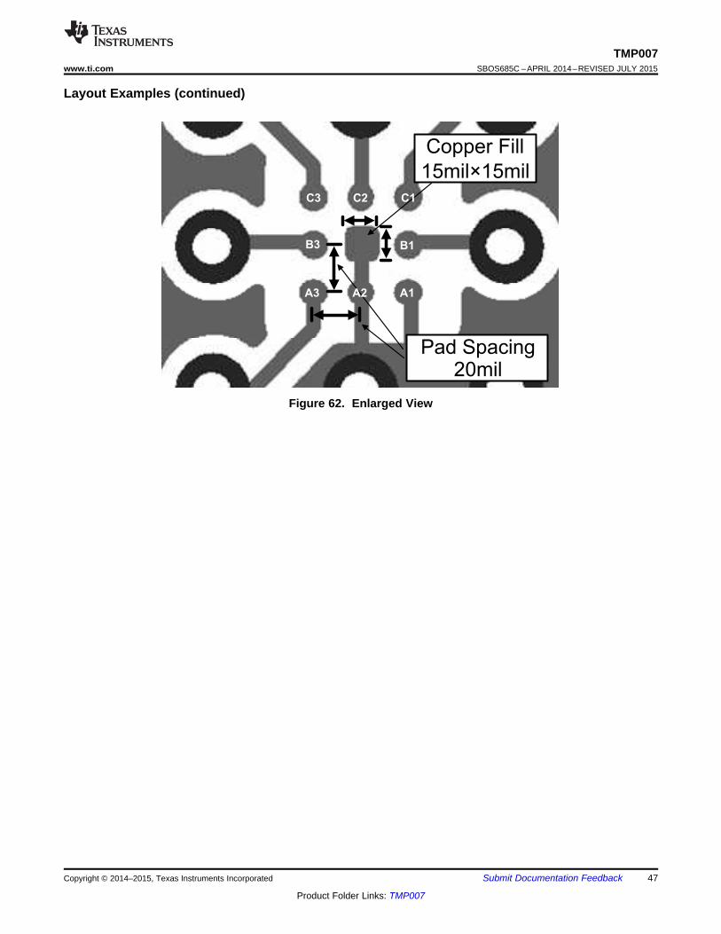
Copper Fill
15mil×15mil
Pad Spacing20mil
B1
A1A2A3
B3
C3 C2 C1
47
TMP007www.ti.com SBOS685C –APRIL 2014–REVISED JULY 2015
Product Folder Links: TMP007
Submit Documentation FeedbackCopyright © 2014–2015, Texas Instruments Incorporated
Layout Examples (continued)
Figure 62. Enlarged View
48
TMP007SBOS685C –APRIL 2014–REVISED JULY 2015 www.ti.com
Product Folder Links: TMP007
Submit Documentation Feedback Copyright © 2014–2015, Texas Instruments Incorporated
11 Device and Documentation Support
11.1 Device Support
11.1.1 Device NomenclatureThe device performance is characterized by the signal, responsivity, and the noise of the sensor. The sensornoise can be characterized in terms of the raw sensor voltage, or in terms of a reference system with knownoptical transfer function.
Responsivity A measure of the voltage generated by the thermopile as a function of the thermal radiationincident on the device. The responsivity is measured in V/W. Typically incident radiations are in µWand sensor output voltages in µV.
Sensor Noise The noise voltage intrinsic to the sensor given in nV. This parameter is conversion-timedependent.
Noise Equivalent Power (NEP) The smallest thermal power difference that the detector can reliably detect;measured in nW. The NEP is a function of the sensor noise and the responsivity.
Noise Equivalent Temperature Difference (NETD) The smallest temperature difference the detector canreliably detect; measured in milliKelvins (mK). The NETD is a function of the sensor noise,responsivity and the system specific optical path.
For comparison purposes, NETD is given for a reference system without a lens and with anideal (nonabsorbing) F/1 lens.
11.2 Documentation Support
11.2.1 Related DocumentationSBOU142 — TMP007 Calibration Guide.
SBOU143 — TMP007 Layout and Assembly Guide.
11.3 Community ResourcesThe following links connect to TI community resources. Linked contents are provided AS IS by the respectivecontributors. They do not constitute TI specifications and do not necessarily reflect TI's views; see TI's Terms ofUse.
TI E2E™ Online Community TI's Engineer-to-Engineer (E2E) Community. Created to foster collaborationamong engineers. At e2e.ti.com, you can ask questions, share knowledge, explore ideas and helpsolve problems with fellow engineers.
Design Support TI's Design Support Quickly find helpful E2E forums along with design support tools andcontact information for technical support.
11.4 TrademarksE2E is a trademark of Texas Instruments.All other trademarks are the property of their respective owners.
11.5 Electrostatic Discharge CautionThis integrated circuit can be damaged by ESD. Texas Instruments recommends that all integrated circuits be handled withappropriate precautions. Failure to observe proper handling and installation procedures can cause damage.
ESD damage can range from subtle performance degradation to complete device failure. Precision integrated circuits may be moresusceptible to damage because very small parametric changes could cause the device not to meet its published specifications.
11.6 GlossarySLYZ022 — TI Glossary.
This glossary lists and explains terms, acronyms, and definitions.

49
TMP007www.ti.com SBOS685C –APRIL 2014–REVISED JULY 2015
Product Folder Links: TMP007
Submit Documentation FeedbackCopyright © 2014–2015, Texas Instruments Incorporated
12 Mechanical, Packaging, and Orderable InformationThe following pages include mechanical, packaging, and orderable information. This information is the mostcurrent data available for the designated devices. This data is subject to change without notice and revision ofthis document. For browser-based versions of this data sheet, refer to the left-hand navigation.

PACKAGE OPTION ADDENDUM
www.ti.com 22-Aug-2017
Addendum-Page 1
PACKAGING INFORMATION
Orderable Device Status(1)
Package Type PackageDrawing
Pins PackageQty
Eco Plan(2)
Lead/Ball Finish(6)
MSL Peak Temp(3)
Op Temp (°C) Device Marking(4/5)
Samples
TMP007AIYZFR NRND DSBGA YZF 8 3000 Green (RoHS& no Sb/Br)
SNAGCU Level-2-260C-1 YEAR -40 to 125 TMP007
TMP007AIYZFT NRND DSBGA YZF 8 250 Green (RoHS& no Sb/Br)
SNAGCU Level-2-260C-1 YEAR -40 to 125 TMP007
(1) The marketing status values are defined as follows:ACTIVE: Product device recommended for new designs.LIFEBUY: TI has announced that the device will be discontinued, and a lifetime-buy period is in effect.NRND: Not recommended for new designs. Device is in production to support existing customers, but TI does not recommend using this part in a new design.PREVIEW: Device has been announced but is not in production. Samples may or may not be available.OBSOLETE: TI has discontinued the production of the device.
(2) RoHS: TI defines "RoHS" to mean semiconductor products that are compliant with the current EU RoHS requirements for all 10 RoHS substances, including the requirement that RoHS substancedo not exceed 0.1% by weight in homogeneous materials. Where designed to be soldered at high temperatures, "RoHS" products are suitable for use in specified lead-free processes. TI mayreference these types of products as "Pb-Free".RoHS Exempt: TI defines "RoHS Exempt" to mean products that contain lead but are compliant with EU RoHS pursuant to a specific EU RoHS exemption.Green: TI defines "Green" to mean the content of Chlorine (Cl) and Bromine (Br) based flame retardants meet JS709B low halogen requirements of <=1000ppm threshold. Antimony trioxide basedflame retardants must also meet the <=1000ppm threshold requirement.
(3) MSL, Peak Temp. - The Moisture Sensitivity Level rating according to the JEDEC industry standard classifications, and peak solder temperature.
(4) There may be additional marking, which relates to the logo, the lot trace code information, or the environmental category on the device.
(5) Multiple Device Markings will be inside parentheses. Only one Device Marking contained in parentheses and separated by a "~" will appear on a device. If a line is indented then it is a continuationof the previous line and the two combined represent the entire Device Marking for that device.
(6) Lead/Ball Finish - Orderable Devices may have multiple material finish options. Finish options are separated by a vertical ruled line. Lead/Ball Finish values may wrap to two lines if the finishvalue exceeds the maximum column width.
Important Information and Disclaimer:The information provided on this page represents TI's knowledge and belief as of the date that it is provided. TI bases its knowledge and belief on informationprovided by third parties, and makes no representation or warranty as to the accuracy of such information. Efforts are underway to better integrate information from third parties. TI has taken andcontinues to take reasonable steps to provide representative and accurate information but may not have conducted destructive testing or chemical analysis on incoming materials and chemicals.TI and TI suppliers consider certain information to be proprietary, and thus CAS numbers and other limited information may not be available for release.
In no event shall TI's liability arising out of such information exceed the total purchase price of the TI part(s) at issue in this document sold by TI to Customer on an annual basis.

PACKAGE OPTION ADDENDUM
www.ti.com 22-Aug-2017
Addendum-Page 2

TAPE AND REEL INFORMATION
*All dimensions are nominal
Device PackageType
PackageDrawing
Pins SPQ ReelDiameter
(mm)
ReelWidth
W1 (mm)
A0(mm)
B0(mm)
K0(mm)
P1(mm)
W(mm)
Pin1Quadrant
TMP007AIYZFR DSBGA YZF 8 3000 180.0 8.4 2.07 2.07 0.81 4.0 8.0 Q1
TMP007AIYZFT DSBGA YZF 8 250 180.0 8.4 2.07 2.07 0.81 4.0 8.0 Q1
PACKAGE MATERIALS INFORMATION
www.ti.com 23-Aug-2017
Pack Materials-Page 1

*All dimensions are nominal
Device Package Type Package Drawing Pins SPQ Length (mm) Width (mm) Height (mm)
TMP007AIYZFR DSBGA YZF 8 3000 210.0 185.0 35.0
TMP007AIYZFT DSBGA YZF 8 250 210.0 185.0 35.0
PACKAGE MATERIALS INFORMATION
www.ti.com 23-Aug-2017
Pack Materials-Page 2

D: Max =
E: Max =
1.918 mm, Min =
1.898 mm, Min =
1.858 mm
1.838 mm

IMPORTANT NOTICE
Texas Instruments Incorporated (TI) reserves the right to make corrections, enhancements, improvements and other changes to itssemiconductor products and services per JESD46, latest issue, and to discontinue any product or service per JESD48, latest issue. Buyersshould obtain the latest relevant information before placing orders and should verify that such information is current and complete.TI’s published terms of sale for semiconductor products (http://www.ti.com/sc/docs/stdterms.htm) apply to the sale of packaged integratedcircuit products that TI has qualified and released to market. Additional terms may apply to the use or sale of other types of TI products andservices.Reproduction of significant portions of TI information in TI data sheets is permissible only if reproduction is without alteration and isaccompanied by all associated warranties, conditions, limitations, and notices. TI is not responsible or liable for such reproduceddocumentation. Information of third parties may be subject to additional restrictions. Resale of TI products or services with statementsdifferent from or beyond the parameters stated by TI for that product or service voids all express and any implied warranties for theassociated TI product or service and is an unfair and deceptive business practice. TI is not responsible or liable for any such statements.Buyers and others who are developing systems that incorporate TI products (collectively, “Designers”) understand and agree that Designersremain responsible for using their independent analysis, evaluation and judgment in designing their applications and that Designers havefull and exclusive responsibility to assure the safety of Designers' applications and compliance of their applications (and of all TI productsused in or for Designers’ applications) with all applicable regulations, laws and other applicable requirements. Designer represents that, withrespect to their applications, Designer has all the necessary expertise to create and implement safeguards that (1) anticipate dangerousconsequences of failures, (2) monitor failures and their consequences, and (3) lessen the likelihood of failures that might cause harm andtake appropriate actions. Designer agrees that prior to using or distributing any applications that include TI products, Designer willthoroughly test such applications and the functionality of such TI products as used in such applications.TI’s provision of technical, application or other design advice, quality characterization, reliability data or other services or information,including, but not limited to, reference designs and materials relating to evaluation modules, (collectively, “TI Resources”) are intended toassist designers who are developing applications that incorporate TI products; by downloading, accessing or using TI Resources in anyway, Designer (individually or, if Designer is acting on behalf of a company, Designer’s company) agrees to use any particular TI Resourcesolely for this purpose and subject to the terms of this Notice.TI’s provision of TI Resources does not expand or otherwise alter TI’s applicable published warranties or warranty disclaimers for TIproducts, and no additional obligations or liabilities arise from TI providing such TI Resources. TI reserves the right to make corrections,enhancements, improvements and other changes to its TI Resources. TI has not conducted any testing other than that specificallydescribed in the published documentation for a particular TI Resource.Designer is authorized to use, copy and modify any individual TI Resource only in connection with the development of applications thatinclude the TI product(s) identified in such TI Resource. NO OTHER LICENSE, EXPRESS OR IMPLIED, BY ESTOPPEL OR OTHERWISETO ANY OTHER TI INTELLECTUAL PROPERTY RIGHT, AND NO LICENSE TO ANY TECHNOLOGY OR INTELLECTUAL PROPERTYRIGHT OF TI OR ANY THIRD PARTY IS GRANTED HEREIN, including but not limited to any patent right, copyright, mask work right, orother intellectual property right relating to any combination, machine, or process in which TI products or services are used. Informationregarding or referencing third-party products or services does not constitute a license to use such products or services, or a warranty orendorsement thereof. Use of TI Resources may require a license from a third party under the patents or other intellectual property of thethird party, or a license from TI under the patents or other intellectual property of TI.TI RESOURCES ARE PROVIDED “AS IS” AND WITH ALL FAULTS. TI DISCLAIMS ALL OTHER WARRANTIES ORREPRESENTATIONS, EXPRESS OR IMPLIED, REGARDING RESOURCES OR USE THEREOF, INCLUDING BUT NOT LIMITED TOACCURACY OR COMPLETENESS, TITLE, ANY EPIDEMIC FAILURE WARRANTY AND ANY IMPLIED WARRANTIES OFMERCHANTABILITY, FITNESS FOR A PARTICULAR PURPOSE, AND NON-INFRINGEMENT OF ANY THIRD PARTY INTELLECTUALPROPERTY RIGHTS. TI SHALL NOT BE LIABLE FOR AND SHALL NOT DEFEND OR INDEMNIFY DESIGNER AGAINST ANY CLAIM,INCLUDING BUT NOT LIMITED TO ANY INFRINGEMENT CLAIM THAT RELATES TO OR IS BASED ON ANY COMBINATION OFPRODUCTS EVEN IF DESCRIBED IN TI RESOURCES OR OTHERWISE. IN NO EVENT SHALL TI BE LIABLE FOR ANY ACTUAL,DIRECT, SPECIAL, COLLATERAL, INDIRECT, PUNITIVE, INCIDENTAL, CONSEQUENTIAL OR EXEMPLARY DAMAGES INCONNECTION WITH OR ARISING OUT OF TI RESOURCES OR USE THEREOF, AND REGARDLESS OF WHETHER TI HAS BEENADVISED OF THE POSSIBILITY OF SUCH DAMAGES.Unless TI has explicitly designated an individual product as meeting the requirements of a particular industry standard (e.g., ISO/TS 16949and ISO 26262), TI is not responsible for any failure to meet such industry standard requirements.Where TI specifically promotes products as facilitating functional safety or as compliant with industry functional safety standards, suchproducts are intended to help enable customers to design and create their own applications that meet applicable functional safety standardsand requirements. Using products in an application does not by itself establish any safety features in the application. Designers mustensure compliance with safety-related requirements and standards applicable to their applications. Designer may not use any TI products inlife-critical medical equipment unless authorized officers of the parties have executed a special contract specifically governing such use.Life-critical medical equipment is medical equipment where failure of such equipment would cause serious bodily injury or death (e.g., lifesupport, pacemakers, defibrillators, heart pumps, neurostimulators, and implantables). Such equipment includes, without limitation, allmedical devices identified by the U.S. Food and Drug Administration as Class III devices and equivalent classifications outside the U.S.TI may expressly designate certain products as completing a particular qualification (e.g., Q100, Military Grade, or Enhanced Product).Designers agree that it has the necessary expertise to select the product with the appropriate qualification designation for their applicationsand that proper product selection is at Designers’ own risk. Designers are solely responsible for compliance with all legal and regulatoryrequirements in connection with such selection.Designer will fully indemnify TI and its representatives against any damages, costs, losses, and/or liabilities arising out of Designer’s non-compliance with the terms and provisions of this Notice.
Mailing Address: Texas Instruments, Post Office Box 655303, Dallas, Texas 75265Copyright © 2017, Texas Instruments Incorporated