infrared optical properties of amorphous and ...tanner/pdfs/bright13jap-ta2o5-films.pdf · infrared...
TRANSCRIPT

Infrared optical properties of amorphous and nanocrystalline Ta2O5
thin films
T. J. Bright,1 J. I. Watjen,1 Z. M. Zhang,1,a) C. Muratore,2,3 A. A. Voevodin,2 D. I. Koukis,4
D. B. Tanner,4 and D. J. Arenas5
1George W. Woodruff School of Mechanical Engineering, Georgia Institute of Technology, Atlanta,Georgia 30332, USA2Nanoelectronic Materials Branch, Materials and Manufacturing Directorate,Air Force Research Laboratory, Wright Patterson AFB, Ohio 45433, USA3Department of Chemical and Materials Engineering, University of Dayton, Dayton, Ohio 45469, USA4Department of Physics, University of Florida, Gainesville, Florida 32611, USA5Department of Physics, University of North Florida, Jacksonville, Florida 32254, USA
(Received 12 December 2012; accepted 11 August 2013; published online 28 August 2013)
The optical constants of tantalum pentoxide (Ta2O5) are determined in a broad spectral region from
the visible to the far infrared. Ta2O5 films of various thicknesses from approximately 170 to
1600 nm are deposited using reactive magnetron sputtering on Si substrates. X-ray diffraction
shows that the as-deposited films are amorphous, and annealing in air at 800 �C results in the
formation of nanocrystalline Ta2O5. Ellipsometry is used to obtain the dispersion in the visible and
near-infrared. Two Fourier-transform infrared spectrometers are used to measure the transmittance
and reflectance at wavelengths from 1 to 1000 lm. The surface topography and microstructure of
the samples are examined using atomic force microscopy, confocal microscopy, and scanning
electron microscopy. Classical Lorentz oscillators are employed to model the absorption bands due
to phonons and impurities. A simple model is introduced to account for light scattering in the
annealed films, which contain micro-cracks. For the unannealed samples, an effective-medium
approximation is used to take into account the adsorbed moisture in the film and a Drude free-
electron term is also added to model the broad background absorption. VC 2013 AIP Publishing LLC.
[http://dx.doi.org/10.1063/1.4819325]
I. INTRODUCTION
Tantalum pentoxide (Ta2O5) is a high refractive index
dielectric with chemical stability at high temperatures and a
melting point of 1785 �C, and is thus suitable for high-
temperature applications. Ta2O5 films have been used or have
potential applications in thin-film capacitors,1 microelec-
tronics,2 anti-reflection coatings,3 multilayer optical coat-
ings,4,5 corrosion resistant protective coatings,5 and infrared
(IR) emissivity modulating devices.6 Knowledge of the opti-
cal properties of Ta2O5 is needed for the design of devices
that tailor radiative properties such as anti-reflection and mul-
tilayer coatings.
Ta2O5 films can be deposited by various methods of
physical vapor deposition (PVD) or chemical vapor deposi-
tion (CVD).2 Different deposition methods may result in
films that have an amorphous phase (a-Ta2O5) or two distinct
crystal phases depending on the annealing, that is, an ortho-
rhombic b-Ta2O5 and a hexagonal d-Ta2O5.2,7 In addition,
there is also a high-temperature tetragonal a-Ta2O5 phase
that forms at temperatures of approximately 1360 �C.8 Phase
transformation at much lower temperatures can also occur in
nanostructured Ta2O5.9 The majority of literature on the op-
tical constants has concentrated on the ultraviolet (UV), visi-
ble, and near-IR properties.4,10–14 The optical constants for a
variety of dielectric films, deposited using electron-beam
evaporation, have been determined and tabulated from 0.6 to
12 lm in Ref. 15. It was shown that Ta2O5 has a refractive
index around 2.0 with negligible absorption from 0.6 up to
10 lm.15 Chandrasekharan et al.16 reported the mid-IR prop-
erties of Ta2O5 films and studied the development of a SiO2
layer at the interface between the film and the Si substrate
due to heat treatment. Franke et al.17,18 investigated the opti-
cal properties of amorphous and crystalline Ta2O5 films
from the deep-UV to far-IR using spectroscopic ellipsome-
try. The dielectric function was modeled based on the line-
shape analysis up to a wavelength of 40 lm. However, strong
phonon modes exist in Ta2O5 at wavenumbers between 200
and 300 cm�1 (or wavelengths from 50 to 33 lm).19 In order
to fully describe the far-IR dielectric function of Ta2O5 films,
it is imperative to consider these phonon modes in the dielec-
tric function model. The study of the far-IR properties of
materials may be useful in designing absorption-based filters
as well as in understanding the atomic bonding structures.19
In this work, the dielectric functions of amorphous and
nanocrystalline Ta2O5 films are determined, at wavenumbers
from 10 to 20 000 cm�1, by analyzing ellipsometric measure-
ments in the visible and near-IR regions and by fitting the
transmittance and reflectance measured with Fourier-
transform IR (FTIR) spectrometers from the near- to far-IR
regions. Thin Ta2O5 films are deposited on Si substrates
using reactive magnetron sputtering. The phase and structure
of the as-deposited and annealed samples are also character-
ized. The location and strength of individual phonon bandsa)Electronic mail: [email protected]
0021-8979/2013/114(8)/083515/10/$30.00 VC 2013 AIP Publishing LLC114, 083515-1
JOURNAL OF APPLIED PHYSICS 114, 083515 (2013)
Downloaded 28 Aug 2013 to 128.227.240.170. This article is copyrighted as indicated in the abstract. Reuse of AIP content is subject to the terms at: http://jap.aip.org/about/rights_and_permissions

are determined in the mid- and far-infrared regions. The effect
of cracking in the annealed films is considered using a
volume-scattering model. The effects of free carriers and
adsorbed water moisture in the amorphous films are also con-
sidered in the development of the dielectric function model.
II. SAMPLE FABRICATION AND CHARACTERIZATION
A magnetron sputtering system, described previously,20
was used to deposit thin Ta2O5 films on Si substrates. The
films were reactively sputtered from a Ta target of 99.9% pu-
rity in an Ar/O2 environment to facilitate the reactive forma-
tion of the oxide. During the deposition process, the power
was maintained at 30 W and the substrate temperature was
held at 100 �C. The flow rates of Ar and O2 gases with
99.999% purity were 22 sccm and 2.5 sccm, respectively.
The substrate thickness and properties are different for some
of the samples. Detailed parameters of the six samples used
for the present study are listed in Table I. Two of them were
left as-deposited and the rest were annealed in air at 800 �Cfor 1 h. The deposition parameters such as gas flow rates and
substrate temperature were chosen according to the
literature21–26 in order to obtain high-quality Ta2O5 films.
X-ray diffraction (XRD) measurements of the annealed
and as-deposited samples were performed using a Rigaku
D-Max diffractometer in a Bragg-Brentano configuration. A
test film was annealed at various temperatures in air.
Annealing in air at 800 �C for 1 h yielded well-defined XRD
patterns; therefore, all the annealed samples were treated
under the same annealing condition. Figure 1 shows the
XRD profile for TaO-3a that matches well with the ortho-
rhombic b-phase (JCPDS: 25-0922), although some closely
spaced peaks appear to be merged due to broadening.7,27,28
The prominent peak in the (001) plane suggests an aniso-
tropic crystalline orientation due to the stress effect. Similar
results were obtained for other annealed samples, but are not
shown. It should be noted that there exists a hexagonal
d-phase of Ta2O5 (JCPDS: 19-1299) that has a diffraction
pattern nearly overlapping that of the b-phase Ta2O5.7,8 Both
of these crystal phases are reported to occur in the literature
at annealing temperatures close to that used in the present
study.2,7,8,27,28 Hence, it is possible that both phases exist in
the annealed films. The identification of the b-phase is con-
firmed by the broadness of the peaks and the existence of
several minor peaks in the XRD pattern. Therefore, it is pre-
sumed that the annealed samples are primarily orthorhombic
b-phase. The XRD peak associated with (001) plane in Fig. 1
is used to estimate the crystalline size, which is about 40 nm,
according to Scherrer’s formula.29 Hence the annealed films
are identified as containing nanocrystalline Ta2O5. Note that
the peaks at 2h¼ 29� and 37� are broadened due to the merg-
ing of multiple diffraction orders. The unannealed or as-
deposited samples are amorphous as there are no distinct
peaks in the XRD profiles, which are not shown here. To ver-
ify the composition of the fabricated films, X-ray photoelec-
tron spectroscopy (XPS) was performed for an annealed and
an unannealed sample after all the spectroscopic measure-
ments. The samples were heated to 200 �C in ultrahigh vac-
uum to remove surface water. The analysis of the XPS data
for the Ta 4f peak position and the area ratio of Ta 4f and O
1s peaks reveals close to stoichiometric Ta2O5 in both the
annealed and unannealed samples.
The surface topography of the samples was measured
using a Veeco Dimension 3100 Atomic Force Microscope
(AFM) in tapping mode over an area of either 4� 4 lm2 or
3� 3 lm2. The AFM probe is an uncoated n-type Si probe
whose tip radius is 10 nm. The measured roughness for each
TABLE I. Sample identification (ID) and parameters. In the sample ID, the
last letter “u” indicates that it was unannealed (or as-deposited) and “a” indi-
cates that it was annealed at 800 �C in air for 1 h. The unannealed Ta2O5
samples TaO-1u and TaO-2u are amorphous. The annealed four samples are
nanocrystalline Ta2O5. The RMS roughness of the film is obtained from
AFM.
Sample ID
Substrate
thickness
(lm)
RMS
roughness
(nm)
Film thickness
(Ellipsometry)
(nm)
Film thickness
(FTIR)
(nm)
TaO-lu 432 4.1 1588 1589
TaO-2u 432 2.6 492 506
TaO-3a 432 14.5 1017 1035
TaO-4a 432 20.4 462 478
TaO-5a 750 3.6 347 353
TaO-6a 750 3.3 174 179
FIG. 1. X-ray diffraction profile of an annealed Ta2O5, sample TaO-3a, also
shown are the powder diffraction files for d-Ta2O5 and b-Ta2O5. Other
annealed samples show nearly identical XRD profiles. Note that the as-
deposited samples do not show any peaks in their XRD profiles, which are
therefore not shown here.
083515-2 Bright et al. J. Appl. Phys. 114, 083515 (2013)
Downloaded 28 Aug 2013 to 128.227.240.170. This article is copyrighted as indicated in the abstract. Reuse of AIP content is subject to the terms at: http://jap.aip.org/about/rights_and_permissions

sample is listed in Table I. The AFM topography of two sam-
ples is shown in Fig. 2. The unannealed sample TaO-2u,
shown in Fig. 2(a), does not contain any cracks. The presence
of cracks can clearly be seen in Fig. 2(b) for the annealed
sample TaO-3a. As can be seen from the AFM images and
Table I, the cracks have increased the root-mean-square
(RMS) roughness that significantly exceeds the actual local
surface roughness. Similar cracks in annealed Ta2O5 films
have been reported by other researchers. The crack develop-
ment is mainly due to the considerable mismatch between the
thermal expansion coefficients of Ta2O5 (4.68� 10�6 K�1)
and the Si substrate (1.10� 10�6 K�1). The mismatch was
reported in the literature as the main contributor to both stress
and refractive index variation for the Ta2O5 films.30 The com-
pressive stress develops as the sample is heated to the anneal-
ing temperature, while the tensile stress develops during the
sample cooling. For the two thinnest films, samples TaO-5a
and TaO-6a, the stress may not be significant enough and
hence the RMS roughness is on the same order as that of the
amorphous films.
In addition, images of the surfaces were taken with an
Olympus LEXT 3D Material Confocal Microscope over a
larger surface area of 43� 43 lm2. Two microscope images
are displayed in Fig. 3. Figure 3(a) shows the unannealed
sample, TaO-2u, which has a much smoother surface and no
cracking. Figure 3(b) shows the surface of an annealed sam-
ple TaO-3a. The scaly appearance is due to cracking that
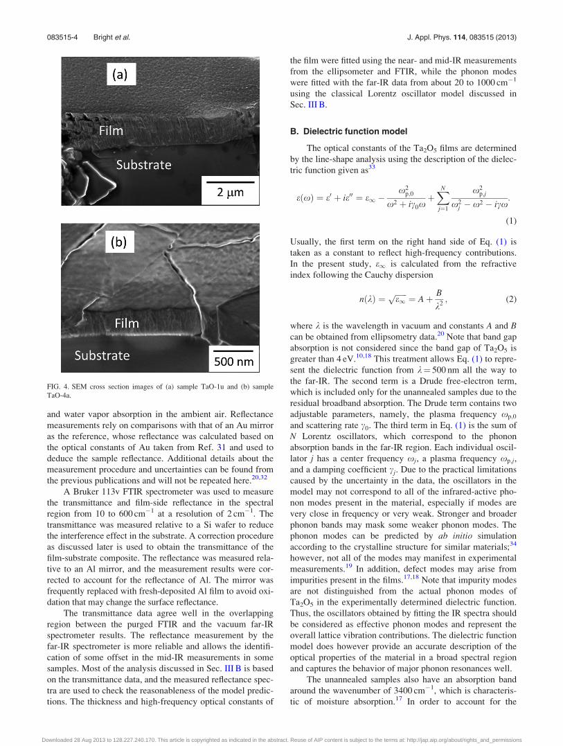
occurs during annealing. Cross-sectional images of two films
were also taken using scanning electron microscopy (SEM)
at an inclined angle of approximately 45� to study their
microstructure, as shown in Fig. 4. The unannealed sample
TaO-1u, shown in Fig. 4(a), does not display significant
cracking or roughness. It can be seen in Fig. 4(b) that the
annealed sample TaO-4a contains cracks that penetrate
through the film. These cracks contribute to volumetric scat-
tering and optical losses in the sample and need to be
included in the modeling of the radiative properties that will
be discussed in Sec. III C.
III. SPECTROSCOPIC MEASUREMENTSAND ANALYSIS
A. Instrumentation
A J.A. Woollam M-2000 ellipsometer was used to per-
form variable angle, room temperature ellipsometry meas-
urements of the Ta2O5 samples in the wavelength range from
500 to 1000 nm with a resolution of 1.6 nm. Data for three
incidence angles (65�, 70�, and 75�) were collected and used
to extract the thickness and dispersion of each film in the
visible and near-IR regions. The built-in algorithm in the
CompleteEase software was used to optimize the regression
parameters as well as to estimate the standard error in the
ellipsometry parameters of the fitting.
An ABB Bomem FTLA-2000 FTIR was used to mea-
sure the normal transmittance of the Ta2O5 samples as well
as the near normal reflectance of the samples for incidence
on either the substrate or the film side at room temperature.
Measurements were taken in the wavenumber range from
approximately 500 to 10 000 cm�1 at 4 cm�1 resolution. The
spectrometer was purged with nitrogen gas to minimize CO2FIG. 2. AFM topographies of (a) sample TaO-2u and (b) sample TaO-3a.
FIG. 3. Confocal microscope images of (a) sample TaO-2u and (b) sample
TaO-3a.
083515-3 Bright et al. J. Appl. Phys. 114, 083515 (2013)
Downloaded 28 Aug 2013 to 128.227.240.170. This article is copyrighted as indicated in the abstract. Reuse of AIP content is subject to the terms at: http://jap.aip.org/about/rights_and_permissions
and water vapor absorption in the ambient air. Reflectance
measurements rely on comparisons with that of an Au mirror
as the reference, whose reflectance was calculated based on
the optical constants of Au taken from Ref. 31 and used to
deduce the sample reflectance. Additional details about the
measurement procedure and uncertainties can be found from
the previous publications and will not be repeated here.20,32
A Bruker 113v FTIR spectrometer was used to measure
the transmittance and film-side reflectance in the spectral
region from 10 to 600 cm�1 at a resolution of 2 cm�1. The
transmittance was measured relative to a Si wafer to reduce
the interference effect in the substrate. A correction procedure
as discussed later is used to obtain the transmittance of the
film-substrate composite. The reflectance was measured rela-
tive to an Al mirror, and the measurement results were cor-
rected to account for the reflectance of Al. The mirror was
frequently replaced with fresh-deposited Al film to avoid oxi-
dation that may change the surface reflectance.
The transmittance data agree well in the overlapping
region between the purged FTIR and the vacuum far-IR
spectrometer results. The reflectance measurement by the
far-IR spectrometer is more reliable and allows the identifi-
cation of some offset in the mid-IR measurements in some
samples. Most of the analysis discussed in Sec. III B is based
on the transmittance data, and the measured reflectance spec-
tra are used to check the reasonableness of the model predic-
tions. The thickness and high-frequency optical constants of
the film were fitted using the near- and mid-IR measurements
from the ellipsometer and FTIR, while the phonon modes
were fitted with the far-IR data from about 20 to 1000 cm�1
using the classical Lorentz oscillator model discussed in
Sec. III B.
B. Dielectric function model
The optical constants of the Ta2O5 films are determined
by the line-shape analysis using the description of the dielec-
tric function given as33
eðxÞ ¼ e0 þ ie00 ¼ e1 �x2
p;0
x2 þ ic0xþXN
j¼1
x2p;j
x2j � x2 � icx
:
(1)
Usually, the first term on the right hand side of Eq. (1) is
taken as a constant to reflect high-frequency contributions.
In the present study, e1 is calculated from the refractive
index following the Cauchy dispersion
nðkÞ ¼ ffiffiffiffiffiffie1p ¼ Aþ B
k2; (2)
where k is the wavelength in vacuum and constants A and Bcan be obtained from ellipsometry data.20 Note that band gap
absorption is not considered since the band gap of Ta2O5 is
greater than 4 eV.10,18 This treatment allows Eq. (1) to repre-
sent the dielectric function from k¼ 500 nm all the way to
the far-IR. The second term is a Drude free-electron term,
which is included only for the unannealed samples due to the
residual broadband absorption. The Drude term contains two
adjustable parameters, namely, the plasma frequency xp;0
and scattering rate c0. The third term in Eq. (1) is the sum of
N Lorentz oscillators, which correspond to the phonon
absorption bands in the far-IR region. Each individual oscil-
lator j has a center frequency xj, a plasma frequency xp;j,
and a damping coefficient cj. Due to the practical limitations
caused by the uncertainty in the data, the oscillators in the
model may not correspond to all of the infrared-active pho-
non modes present in the material, especially if modes are
very close in frequency or very weak. Stronger and broader
phonon bands may mask some weaker phonon modes. The
phonon modes can be predicted by ab initio simulation
according to the crystalline structure for similar materials;34
however, not all of the modes may manifest in experimental
measurements.19 In addition, defect modes may arise from
impurities present in the films.17,18 Note that impurity modes
are not distinguished from the actual phonon modes of
Ta2O5 in the experimentally determined dielectric function.
Thus, the oscillators obtained by fitting the IR spectra should
be considered as effective phonon modes and represent the
overall lattice vibration contributions. The dielectric function
model does however provide an accurate description of the
optical properties of the material in a broad spectral region
and captures the behavior of major phonon resonances well.
The unannealed samples also have an absorption band
around the wavenumber of 3400 cm�1, which is characteris-
tic of moisture absorption.17 In order to account for the
FIG. 4. SEM cross section images of (a) sample TaO-1u and (b) sample
TaO-4a.
083515-4 Bright et al. J. Appl. Phys. 114, 083515 (2013)
Downloaded 28 Aug 2013 to 128.227.240.170. This article is copyrighted as indicated in the abstract. Reuse of AIP content is subject to the terms at: http://jap.aip.org/about/rights_and_permissions
existence of moisture in the unannealed samples, the
Bruggeman effective medium approximation (EMA) is used
to determine the effective dielectric function of the film, eeff ,
assuming that a small amount of water is randomly dispersed
in the Ta2O5 film17,35
ð1� f Þ e� eeff
eþ 2eeff
þ few � eeff
ew þ 2eeff
¼ 0; (3)
where f is the volume fraction of water, e is calculated from
Eq. (1), and ew is the dielectric function of water taken from
Downing and Williams.36 Note that the EMA prediction of
eeff is taken as the dielectric function of the moist Ta2O5 film
and is used to calculate the radiative properties of the film-
substrate composite. The additional parameter f is only sensi-
tive in the water absorption region and can be determined by
fitting the transmittance in the near- to mid-IR region.
C. Fitting procedure
In the region for ellipsometry measurements, the Si sub-
strate is opaque and thin-film optics can be used to fit the
ellipsometry parameters W and D according to the ratio of
the Fresnel reflection coefficients for p-polarized (rp) and s-
polarized (rs) waves as follows:17,20
R ¼ rp
rs
¼ tanðWÞexpðiDÞ: (4)
Note that the quantity W is related to the relative intensity of
the reflected lights of the two polarizations and D is the rela-
tive difference of their phases. Both quantities can be calcu-
lated with thin-film optics by assuming a homogeneous thin
film with smooth parallel interfaces on an opaque substrate.
Multiple incidence angles are used to ensure a reliable deter-
mination of parameters A and B in Eq. (2) and the film
thickness.
The transmittance and reflectance spectra obtained by
the FTIR spectrometers were fit using the optical model for a
coherent film on a thick incoherent substrate.33,37 This is a
reasonable assumption considering the relatively low spec-
tral resolution of 4 cm�1 in the near-and mid-IR region. The
transmittance and reflectance for a thin film on a thick sub-
strate can be expressed as follows:38
T ¼ sasssi
1� qsqbs2i
; (5)
Rf ¼ qa þqss
2as
2i
1� qsqbs2i
; (6)
Rs ¼ qs þqbs
2s s
2i
1� qsqbs2i
; (7)
where the subscript f or s in the reflectance R signifies the
film-side or substrate-side incidence. In Eqs. (5)–(7), si is
the internal transmissivity of the substrate, sa and qa are
the transmittance and reflectance at the air-film interface
when the substrate is semi-infinite, qb is the reflectance for
incidence from the substrate at the interface between the
substrate-air, assuming that the substrate is nonabsorbing
and semi-infinite, and ss and qs are the transmittance and re-
flectance at the air-substrate interface when both media are
semi-infinite.33,37,38 Most of the fitting is based on the trans-
mittance only and compared with the reflectance data to con-
firm the fitting results. The reason for using transmittance
only is because the reflectance measurements are subject to a
larger relative uncertainty of around 5%.
The interference effect in the Si substrate is inevitable in
the measured far-IR spectrum. To reduce the interference
effect, the transmittance of the sample was measured relative
to a bare Si substrate. The optical constants of Si were taken
from Ref. 31 and were modified to account for the additional
absorption around 900 cm�1 caused by an O-H band as dis-
cussed previously. Four of the samples were deposited on
432 6 5 lm thick Si substrates with a resistivity of 20 X cm,
and the remaining two were deposited on 750 6 25 lm thick
Si substrates (see Table I) with a resistivity between 10 and
100 X cm as specified by the manufacturer. The resistance of
the thinner Si substrate was determined by fitting the well-
known Drude model for boron-doped Si to the transmittance
of the Si in the far-IR spectrum according to Fu and Zhang39
and references therein. The doping level was thus estimated
to be 6.67 � 1014 cm�3. The transmittance spectrum of Si
calculated from the incoherent formula based on the Drude
model was used to deduce the transmittance data of the sam-
ples in the far-IR region from the relative measurements.
The Drude model is also used to calculate the radiative prop-
erties of the film-substrate composite in the far-IR region
(k> 20 lm) in the line-shape analysis. The effect of the
Drude term is negligible at wavelengths shorter than 20 lm.
It should be noted that the far-IR measurements were not
performed for the last two samples listed in Table I with the
thicker Si substrates. It is shown by comparison with the
transmittance of a bare Si substrate that the optical constants
from Refs. 20 and 31 are suitable for modeling the near- and
mid-IR radiative properties with the thicker substrate, whose
resistivity does not need to be precisely determined.
For the annealed samples with cracks, the transmittance
and the film-side reflectance of the FTIR data exhibit some
attenuation towards the near-IR end of the spectra. Attempts
were initially made to include a surface roughness term
according to the scalar scattering theory.33,40 The predicted
results also showed an attenuation in the substrate-side re-
flectance that contradicts with the experimental observation.
In addition, when the ellipsometry data were analyzed,
accounting for roughness did not improve the fitting.
Therefore, the cracking effect cannot be well described by
surface scattering. A careful examination of Eqs. (5)–(7)
reveals that sa is the only term that appears in T and Rf but
not Rs. A volumetric scattering model is considered in the
final analysis to better model the observed trends due to
cracking of the thick annealed samples, i.e., TaO-3a and
TaO-4a. It is assumed that scattering results in a reduction
only in the transmission through the film, and the attenuation
is wavelength dependent according to
s0a ¼ sa 1� S4f
k4
� �: (8)
083515-5 Bright et al. J. Appl. Phys. 114, 083515 (2013)
Downloaded 28 Aug 2013 to 128.227.240.170. This article is copyrighted as indicated in the abstract. Reuse of AIP content is subject to the terms at: http://jap.aip.org/about/rights_and_permissions
Here, Sf is a fitting parameter that is related to the scattering
cross-sectional area and the defect density, assuming inde-
pendent scattering by small particles that follow Rayleigh
scattering.40,41 When sa in Eqs. (5) and (6) are substituted by
s0a from Eq. (8), both the transmittance and reflectance of the
film side of the sample are reduced, while the substrate-side
reflectance given in Eq. (7) is unaffected. This gives a rea-
sonable interpretation of the experimental results to be dis-
cussed in Sec. IV B. It should be noted that volume
scattering may also arise due to relatively large grains in the
film. Hence, Sf may be considered as an effective lumped
sum of the volume scattering contribution.
The predicted radiative properties are fitted to the meas-
ured FTIR transmittance spectra using a simplex optimiza-
tion algorithm that minimizes the standard error of estimate
(SEE).42,43 It is assumed that e1 is the same as the average
value obtained for either the unannealed or annealed samples
from the ellipsometry data according to Eq. (2). The film
thickness is related to the interference fringes and deter-
mined by fitting the FTIR data in the near- to mid-IR region.
The obtained thickness is then used to fit the parameters in
Eqs. (1) and (3) using far-IR transmittance.
IV. RESULTS AND DISCUSSION
A. Ellipsometric results
The optical constants at wavelengths from 500 to
1000 nm are determined from the ellipsometry data. Each
sample was fit individually to obtain the parameters A and Bin the Cauchy dispersion, Eq. (2), and the film thickness. The
absorption is neglected because the interband transitions occur
at photon energies greater than 4 eV.10,17,18 The resulting Aand B values change little from sample to sample; therefore,
only the averages of all A and B values for the two unannealed
samples and those for the annealed samples are reported here.
For the unannealed samples, the average A and B are 2.06 and
0.025 lm2, respectively. For the annealed samples the average
values of A and B are 2.10 and 0.024 lm2, respectively. All of
the uncertainties in A and B are less than 0.02 and 0.001 lm2,
respectively. Table I shows the thickness obtained from fitting
the ellipsometry data with the Cauchy model. The agreement
between the ellipsometry data and the model is very good for
the unannealed samples as well as for the thinnest annealed
samples. The average mean squared error (MSE) for the two
annealed samples TaO-3a and TaO-4a with cracks is about
five times larger than the rest. However, the coefficients A and
B are all very close. The resulting refractive indices of
n¼ 2.16 and 2.20 for unannealed and annealed Ta2O5 films,
respectively, agree with the typical values reported in the liter-
ature at k¼ 500 nm.4,12–14,17
B. Comparison of the measured and calculatedradiative properties
While e1 in Eq. (1) can be fit using the FTIR data, for
consistency, it is taken instead from the Cauchy dispersion
from Eq. (2) based on ellipsometry measurements. The film
thickness is also fit using near- and mid-IR transmittances,
which are sensitive to the film thickness due to the interference
effect. Despite the existence of cracking, the film thicknesses
obtained from the ellipsometer are quite consistent with those
from the FTIR measurements as shown in Table I. The far-IR
transmittance is used to fit the phonon oscillator parameters
and the results are listed in Table II. For the unannealed sam-
ples, the transmittance measured by FTIR is compared to the
best fit curves as shown in Fig. 5. The agreement is generally
satisfactory throughout the concerned spectral region. The
dips in the far-IR transmission shown in Fig. 5(a) are due to
interaction of light with phonon vibration modes in Ta2O5.
Each of these dips is represented by an oscillator in the dielec-
tric model. Some of the dips may also be caused by the Si sub-
strate especially around 610 cm�1, where there is a dip due to
Si absorption. Due to the uncertainty of the data, very weak
phonon features are difficult to resolve.
The Drude term results in broad absorption and the
plasma frequency and scattering rate are found to be
xp;0¼ 6490 cm�1 and c0¼ 6.5� 105 cm�1 from the fitting.
This extreme broadness can be attributed to the fact that the
samples are amorphous and thus have a very large electron
scattering rate. Based on the Drude parameters, the resistiv-
ity of the sample can be estimated to be 0.9 X cm, which
would be typical of a lightly doped material. The existence
of free electrons in the unannealed samples is presumably
due to a slight oxygen deficiency or sub-stoichiometry dur-
ing the growth process, although other possibilities also
exist.2,6,16 According to Kulisch et al.,44 suboxides of Ta can
contribute to a broadband absorption around 900 cm�1,
which is evident from Fig. 4(a). However, the XPS analysis
does not show any apparent suboxides of Ta in both the
annealed and unannealed samples, suggesting that the oxy-
gen deficiency is insignificant.
The presence of moisture in the film is apparent from
the dip in the transmittance around 3400 cm�1. It is found
using the EMA analysis from Eq. (3) that a volume fraction
of water of 5% works best to model the moisture contribu-
tion to the dielectric function. The addition of water matches
the dip well at 3400 cm�1, but is not broad enough to match
the valley in transmittance. Therefore, another weak oscilla-
tor is added around 3000 cm�1 to the dielectric function
model (j¼ 6 in Table II). This results in satisfactory agree-
ment between the model prediction and the transmittance in
the mid-IR region as shown in Fig. 5(b).
TABLE II. Parameters for the Lorentz oscillators. Note that the parameters
that determine e1 from the ellipsometric measurements are (A¼ 2.06,
B¼ 0.025 lm2 for amorphous Ta2O5; A¼ 2.10, B¼ 0.024 lm2 for nanocrys-
talline Ta2O5).
Amorphous Nanocrystalline
j xj (cm�1) xp;j (cm�1) cj (cm�1) xj (cm�1) xp;j (cm�1) cj (cm�1)
1 266 1040 188 91 260 74
2 500 573 112 214 844 61
3 609 634 88 324 391 73
4 672 408 43 530 1019 142
5 868 277 113 842 372 114
6 3020 373 652
083515-6 Bright et al. J. Appl. Phys. 114, 083515 (2013)
Downloaded 28 Aug 2013 to 128.227.240.170. This article is copyrighted as indicated in the abstract. Reuse of AIP content is subject to the terms at: http://jap.aip.org/about/rights_and_permissions

The thicker film sample, TaO-1u, exhibits more interfer-
ence fringes than the thinner film sample, TaO-2u. The free
spectral range or wavenumber interval between the interfer-
ence maxima can be approximated by 1/(2nd), where d is the
film thickness. Due to absorption around 3000 cm�1, the
transmission of the thicker sample drops quite a bit in this
region. It should be noted that the minimum transmittance
can be estimated from the refractive indices of the film and
substrate if absorption is negligible. The introduction of the
Drude term is necessary to predict the broadband absorption,
allowing the prediction to match the data at the transmittance
minima at 4700, 6250, and 7800 cm�1. Note that the drop in
transmittance close to 10 000 cm�1 is caused by the absorp-
tion of the substrate associated with the indirect band gap of
Si near 1.1 eV.
The transmittance for two of the annealed samples is
shown in Fig. 6. There is no need to include the Drude term
in the dielectric function model, since the samples were
annealed in air: the reaction with oxygen during the anneal-
ing process apparently has improved the stoichiometry. The
annealing has removed the absorbed moisture as well. After
annealing, the low frequency phonon mode at 266 cm�1
shifts to the lower frequencies at 214 cm�1 and becomes nar-
row due to a reduction in the damping coefficient as shown
in Table II. This absorption band becomes much narrower
and deeper as shown in Fig. 6(a). Another phonon mode is
needed to model the small dip around 90 cm�1. From Fig.
6(b), it is evident that there exists a gradual reduction in the
transmittance from 3000 to 10 000 cm�1 and this reduction is
attributed to light scattering due to cracks or grain bounda-
ries inside of the films. The scattering factor Sf for samples
TaO-3a and TaO-4a is determined to be 5.3 and 5.1 nm,
respectively.
Only the two thicker samples require the addition of vol-
ume scattering into the modeling, since cracking was not as
significant in the two thinner samples. As shown in Fig. 7,
the transmittance calculated for TaO-5a and TaO-6a using
the dielectric function model determined for the two thicker
annealed samples agrees well with the measured spectra
without introducing any volume scattering. The far-IR meas-
urements were not performed on samples TaO-5a and TaO-
6a. Strong absorption in the Si substrate near 1100 cm�1 can
be clearly seen in Fig. 7.
Figure 8 compares the measured and calculated reflec-
tance for TaO-3a for both film-side incidence and substrate-
side incidence. There is a gradual attenuation in Rf as shown
in Fig. 8(a), but not in Rs as shown in Fig. 8(b). The substrate-
side reflectance does not show any decrease toward short
wavelengths and this is not typical with surface roughness or
FIG. 5. Transmittance of samples TaO-1u and TaO-2u: (a) far-IR region
from 10 to 1000 cm�1; (b) mid-IR region from 1000 to 10 000 cm�1. FIG. 6. Transmittance of samples TaO-3a and TaO-4a: (a) far-IR region
from 10 to 1000 cm�1; (b) mid-IR region from 1000 to 10 000 cm�1.
083515-7 Bright et al. J. Appl. Phys. 114, 083515 (2013)
Downloaded 28 Aug 2013 to 128.227.240.170. This article is copyrighted as indicated in the abstract. Reuse of AIP content is subject to the terms at: http://jap.aip.org/about/rights_and_permissions

absorption. The volumetric scattering model captures the phe-
nomenon reasonably well, especially considering the simplic-
ity in the model and its assumption of a spherical geometry
and Rayleigh-type independent scattering. The model may
break down in the short wavelength end of the spectrum,
resulting in large disagreement in T and Rf as shown in Figs.
6(b) and 8.
It is worth noting that additional reflectance data was
also collected but not used in the fitting. Since the reflectance
data in the mid-IR region is less reliable than the transmit-
tance data, including them in the fitting would increase the
uncertainty. The largest SEE between the model and the ex-
perimental data for the transmittance of all the samples was
0.023 and the average was 0.014. The agreement between
the reflectance data and the model prediction is good with an
average SEE of 0.024.
C. The dielectric functions
The dielectric function obtained for the amorphous
Ta2O5 films is plotted in Fig. 9 in comparison with that
obtained from Franke et al.17 The results are shown from 10
to 1500 cm�1 since there is little variation beyond 1500 cm�1,
although there are some features due to moisture and the oscil-
lator near 3000 cm�1. Note that the resulting dielectric func-
tion is the effective dielectric function expressed in Eq. (3).
However, in the spectral region shown in the plots, the effect
of 5% water content is negligible, i.e., eeff � e. Toward large
wavenumbers, the real part approaches A2 and the imaginary
part becomes very small. The residual e00 is largely due to the
free-electron contribution. The phonon features can be clearly
seen from the peaks in the imaginary part.33,45 The Drude
term also increases the imaginary part of the dielectric func-
tion toward the smaller wavenumbers. The agreement in the
dielectric function obtained from this work and from Ref. 17
is reasonable at wavenumbers exceeding 600 cm�1. However,
the phonon modes below 500 cm�1 were not resolved in Ref.
17, resulting in a large deviation at smaller wavenumbers.
Figure 10 shows the real and imaginary part of the
dielectric function for the annealed samples, compared with
those from Ref. 18. A distinction from the amorphous Ta2O5
is the sharp peak at the phonon resonance of 214 cm�1 in
the imaginary part. While the oscillator strength defined as
Sj ¼ x2p;j=x
2j is similar to the mode in the amorphous film at
266 cm�1, the reduction in the damping coefficient cj gives
FIG. 7. Transmittance of samples TaO-
5a and TaO-6a. Note that the scale is
zoomed from 500 to 1500 cm�1 to
show features in the far-IR region more
clearly.
FIG. 8. Reflectance of sample TaO-3a: (a) film-side; (b) substrate-side. Note
that the film-side reflectance decreases toward shorter wavelengths due to
scattering, while the substrate-side reflectance is unaffected.
083515-8 Bright et al. J. Appl. Phys. 114, 083515 (2013)
Downloaded 28 Aug 2013 to 128.227.240.170. This article is copyrighted as indicated in the abstract. Reuse of AIP content is subject to the terms at: http://jap.aip.org/about/rights_and_permissions

rise to a narrow band in e00.45 This results in the stronger
absorption observed in the transmittance spectrum shown in
Fig. 6(a). Without the Drude term, the imaginary part is neg-
ligible at wavenumbers exceeding 1000 cm�1. Hence, the
nanocrystalline Ta2O5 has negligible absorption in the visi-
ble to about 10 lm wavelengths. Towards small wavenum-
bers, the imaginary part of the dielectric function drops
quickly without free-electron absorption, as shown in
Fig. 10(b). The real part approaches a dielectric constant of
33 for the annealed films and 23 for the amorphous films.
These values are within the range reported for the low-
frequency (1 MHz) dielectric constants.2,27
V. CONCLUSIONS
The dielectric functions are obtained for amorphous and
nanocrystalline thin film samples of Ta2O5 deposited by
magnetron sputtering. These sputtered films are smooth and
of good structural quality and uniform thickness. Samples
are amorphous as deposited at the substrate temperature used
during deposition. Upon annealing at 800 �C, the samples
become nanocrystalline with an orthorhombic phase being
dominant. This induces a drastic change in the far-IR optical
properties of the film. The low-frequency phonon modes
become much sharper in the nanocrystalline samples. The
frequencies of the effective phonon modes are determined by
a line-shape analysis to quantitatively show the optical pho-
nons in sputtered Ta2O5 films. Thermal stresses in the thicker
samples after annealing were significant enough to cause
cracking and the effect contributes to volume scattering in
the sample thus affecting the near-IR transmittance. A sim-
ple model is introduced to account for the volumetric scatter-
ing in the thin film samples.
ACKNOWLEDGMENTS
This work was mainly sponsored by the Air Force
Research Laboratory Thermal Metamaterials Program.
Additional support was provided to Z. M. Zhang’s group
FIG. 9. Fitted dielectric function of the amorphous Ta2O5, in comparison
with the values from Ref. 17: (a) Real part; (b) Imaginary part.
FIG. 10. Fitted dielectric function of the annealed Ta2O5, in comparison
with the values from Ref. 18: (a) Real part; (b) Imaginary part.
083515-9 Bright et al. J. Appl. Phys. 114, 083515 (2013)
Downloaded 28 Aug 2013 to 128.227.240.170. This article is copyrighted as indicated in the abstract. Reuse of AIP content is subject to the terms at: http://jap.aip.org/about/rights_and_permissions

(for the modeling effort) from the Department of Energy
under Contract No. DE-FG02-06ER46343. We would also
like to thank Michael Jespersen of UDRI/AFRL for help
with the XPS analysis.
1S.-D. Cho and K.-W. Paik, Mater. Sci. Eng., B 67, 108 (1999).2C. Chaneliere, J. L. Autran, R. A. B. Devine, and B. Balland, Mater. Sci.
Eng. R 22, 269–322 (1998).3F. Rubio, J. Denis, J. M. Albella, and J. M. Martinez-Duart, Thin Solid
Films 90, 405 (1982).4A. J. Waldorf, J. A. Dobrowolski, B. T. Sullivan, and L. M. Plante, Appl.
Opt. 32, 5583(1993).5K. Toki, K. Kusakabe, T. Odani, S. Kobuna, and Y. Shimizu, Thin Solid
Films 281–282, 401 (1996).6E. B. Franke, C. L. Trimble, M. Schubert, J. A. Woollam, and J. S. Hale,
Appl. Phys. Lett. 77, 930 (2000).7J. Gonz�alez, M. C. Ruiz, J. B. Rivarola, and D. Pasquevich, J. Mater. Sci.
33, 4173 (1998).8C. Chaneliere, S. Four, J. L. Autran, and R. A. B. Devine, Microelectron.
Reliab. 39, 261 (1999).9R. S. Devan, W.-D. Ho, S. Y. Wu, and Y.-R. Ma, J. Appl. Cryst. 43, 498
(2010).10E. E. Khawaja and S. G. Tomlin, Thin Solid Films 30, 361 (1975).11F. Rubio, J. M. Albella, J. Denis, and J. M. Martinez-Duart, J. Vac. Sci.
Technol. 21, 1043 (1982).12G. A. Al-Jumaily and S. M. Edlou, Thin Solid Films 209, 223 (1992).13E. Atanassova, G. Aygun, R. Turan, and T. Babeva, J. Vac. Sci. Technol. A
24, 206 (2006).14J. Zhou, D. Luo, Y. Li, and Z. Liu, Int. J. Mod. Phys. B 23, 5275 (2009).15J. D. Traylor Kruschwitz and W. T. Pawlewicz, Appl. Opt. 36, 2157 (1997).16R. Chandrasekharan, S. Prakash, M. A. Shannon, and R. I. Masel, J. Heat
Transfer 129, 27 (2007).17E. Franke, C. L. Trimble, M. J. DeVries, J. A. Woollam, M. Schubert, and
F. Frost, J. Appl. Phys. 88, 5166 (2000).18E. Franke, M. Schubert, C. L. Trimble, M. J. DeVries, and J. A. Woollam,
Thin Solid Films 388, 283 (2001).19H. Ono, Y. Hosokawa, and K. Shinoda, Thin Solid Films 381, 57 (2001).20T. J. Bright, J. I. Watjen, Z. M. Zhang, C. Muratore, and A. A. Voevodin,
Thin Solid Films 520, 6793 (2012).21O. D. Vol’pyan and P. P. Yakovlev, J. Opt. Technol. 69, 319 (2002).22E. Atanassova, T. Dimitrova, and J. Koprinarova, Appl. Surf. Sci. 84, 193
(1995).
23S. V. Jagadeesh Chandra, S. Uthanna, and G. Mohan Rao, Appl. Surf. Sci.
254, 1953 (2008).24K. Chen, M. Nielsen, G. R. Yang, E. J. Rymaszewski, and T.-M. Lu,
J. Electron. Mater. 26, 397 (1997).25C. Guoping, L. Lingzhen, Z. Suixin, and Z. Haokang, Vacuum 41, 1204
(1990).26J. M. Ngaruiya, S. Venkataraj, R. Drese, O. Kappertz, T. P. Leervad
Pedersen, and M. Wuttig, Phys. Status Solidi A 198, 99 (2003).27P. C. Joshi and M. W. Cole, J. Appl. Phys. 86, 871 (1999).28T. Dimitrova, K. Arshak, and E. Atanassova, Thin Solid Films 381, 31
(2001).29A. L. Patterson, Phys. Rev. 56, 978 (1939).30S. G. Yoon, Y. T. Kim, H. K. Kim, M. J. Kim, H. M. Lee, and D. H.
Yoon, Mater. Sci. Eng., B 118, 234 (2005).31E. D. Palik, Handbook of Optical Constants of Solids (Academic Press,
San Diego, 1998).32S. Basu, B. J. Lee, and Z. M. Zhang, J. Heat Transfer 132, 023301 (2010).33Z. M. Zhang, Nano/Microscale Heat Transfer (McGraw-Hill Professional,
New York, 2007).34P. Clauws, J. Broeckx, and J. Vennik, Phys. Status Solidi B 131, 459
(1985).35G. L. Carr, S. Perkowitz, and D. B. Tanner, in Infrared and Millimeter
Waves, edited by W. J. Button (Academic Press, Orlando, 1985), pp.
171–263.36H. D. Downing and D. Williams, J. Geophys. Res. 80, 1656, doi:10.1029/
JC080i012p01656 (1975).37B. J. Lee, Z. M. Zhang, E. A. Early, D. P. DeWitt, and B. K. Tsai,
J. Thermophys. Heat Transfer 19, 558 (2005).38Z. M. Zhang, C. J. Fu, and Q. Z. Zhu, Adv. Heat Transfer 37, 179 (2003).39C. J. Fu and Z. M. Zhang, Int. J. Heat Mass Transfer 49, 1703 (2006).40B. J. Lee, V. P. Khuu, and Z. M. Zhang, J. Thermophys. Heat Transfer 19,
360 (2005).41J. R. Howell, R. Siegel, and M. P. Menguc, Thermal Radiation Heat
Transfer, 5th ed. (CRC Press, 2010).42Q. Z. Zhu and Z. M. Zhang, in Nanoparticle Heat Transfer and Fluid
Flow, edited by W. J. Minkowycz, E. M. Sparrow, and J. Abraham (CRC
Press/Taylor&Francis Group, 2012), pp. 143–174.43W. H. Press, Numerical Recipes: The Art of Scientific Computing
(Cambridge University Press, 2007).44W. Kulisch, D. Gilliland, G. Ceccone, L. Sirghi, H. Rauscher, P. N.
Gibson, M. Z€un, F. Bretagnol, and F. Rossi, J. Vac. Sci. Technol. B 27,
1180 (2009).45Z. M. Zhang, B. I. Choi, M. I. Flik, and A. C. Anderson, J. Opt. Soc. Am. B
11, 2252 (1994).
083515-10 Bright et al. J. Appl. Phys. 114, 083515 (2013)
Downloaded 28 Aug 2013 to 128.227.240.170. This article is copyrighted as indicated in the abstract. Reuse of AIP content is subject to the terms at: http://jap.aip.org/about/rights_and_permissions