inductor current zero-crossing detector and ccm/dcm ... · inductor current zero-crossing detector...
TRANSCRIPT
5384 IEEE TRANSACTIONS ON POWER ELECTRONICS, VOL. 29, NO. 10, OCTOBER 2014
Inductor Current Zero-Crossing Detector andCCM/DCM Boundary Detector for Integrated
High-Current Switched-Mode DC–DC ConvertersVratislav Michal
Abstract—This paper presents two circuits that allow us toaccurately detect either the inductor current zero crossing, orthe continuous/discontinous conduction modes boundary in theswitched-mode dc–dc converters. Achieved detection accuracy al-lows us to improve the control and efficiency of the integratedhigh-output current converters, i.e., converters with low-resistancepower switches. Detection is based on the voltage zero-cross de-tector, which provides ideally zero input-referred offset and veryfast results. The concept of voltage polarity detector is based onthe association of a dynamic current mirror and a simple autozerocomparator. This paper describes the main concept of both cir-cuits, aspects of the design allowing us to achieve high accuracy,and presents obtained results. Circuits’ performances are demon-strated on the integrated step-down dc–dc converter with IOUT =2.5 A 30-mΩ NMOS power stage. Measured accuracy of the detec-tion is in order of <15 mA.
Index Terms—Autozero voltage polarity detector, autozero com-parator, continuous/discontinous conduction modes (CCM/DCM)boundary detector, dc–dc converter, pulse-skipping mode, syn-chronous rectifier, zero-cross detector (ZCD).
I. INTRODUCTION
NOWADAYS, high-efficiency switched-mode dc–dc con-verters use the control algorithms, allowing the switching
between continuous conduction mode (CCM) and discontinu-ous conduction mode (DCM). This feature allows us to equalizethe power efficiency for light loads by decreasing both switchingand conduction losses [1], [2]. Usually, when the control part ofthe dc–dc converter detects the predefined boundary, switchingin a low-frequency mode is activated. Typically, low-frequencymodes are the pulse-skipping (PSK) or pulse-frequency modu-lation (PFM). During these low-power modes, the power stageis allowed to be in a high-output-impedance state. At enteringinto the high-impedance state, the inductor’s remaining energyis required to be very low. This allows us to decrease the en-ergy waste caused by substrate diodes of the power transistors’conductions, or by the parasitic oscillations in output VLX node.
The condition allowing us to enter into the low-frequencymode is usually defined by the inversion of the IL inductor
Manuscript received July 29, 2013; revised September 2, 2013 andOctober 14, 2013; accepted November 15, 2013. Date of current version May30, 2014. Recommended for publication by Associate Editor K. Chen.
The author is with the STMicroelectronics, 38000 Grenoble, France (e-mail:[email protected]).
Color versions of one or more of the figures in this paper are available onlineat http://ieeexplore.ieee.org.
Digital Object Identifier 10.1109/TPEL.2013.2292600
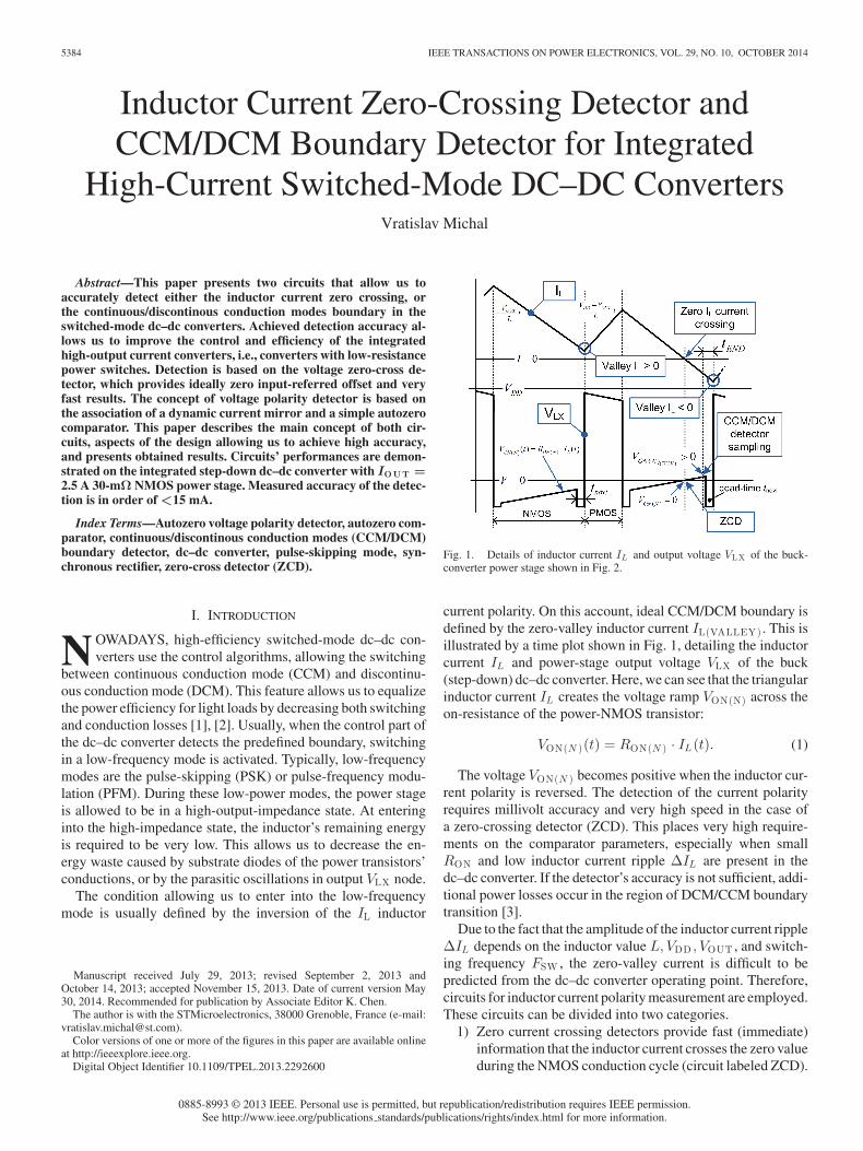
Fig. 1. Details of inductor current IL and output voltage VLX of the buck-converter power stage shown in Fig. 2.
current polarity. On this account, ideal CCM/DCM boundary isdefined by the zero-valley inductor current IL(VALLEY) . This isillustrated by a time plot shown in Fig. 1, detailing the inductorcurrent IL and power-stage output voltage VLX of the buck(step-down) dc–dc converter. Here, we can see that the triangularinductor current IL creates the voltage ramp VON(N) across theon-resistance of the power-NMOS transistor:
VON(N )(t) = RON(N ) · IL (t). (1)
The voltage VON(N ) becomes positive when the inductor cur-rent polarity is reversed. The detection of the current polarityrequires millivolt accuracy and very high speed in the case ofa zero-crossing detector (ZCD). This places very high require-ments on the comparator parameters, especially when smallRON and low inductor current ripple ΔIL are present in thedc–dc converter. If the detector’s accuracy is not sufficient, addi-tional power losses occur in the region of DCM/CCM boundarytransition [3].
Due to the fact that the amplitude of the inductor current rippleΔIL depends on the inductor value L, VDD , VOUT , and switch-ing frequency FSW , the zero-valley current is difficult to bepredicted from the dc–dc converter operating point. Therefore,circuits for inductor current polarity measurement are employed.These circuits can be divided into two categories.
1) Zero current crossing detectors provide fast (immediate)information that the inductor current crosses the zero valueduring the NMOS conduction cycle (circuit labeled ZCD).
0885-8993 © 2013 IEEE. Personal use is permitted, but republication/redistribution requires IEEE permission.See http://www.ieee.org/publications standards/publications/rights/index.html for more information.
MICHAL: INDUCTOR CURRENT ZERO-CROSSING DETECTOR AND CCM/DCM BOUNDARY DETECTOR 5385
2) Negative IL valley current detectors measure the inductorcurrent polarity at the end of the NMOS conduction cycleand provide the output information afterward (circuit la-beled here as CCM/DCM boundary detector). This circuitdoes not require fast detection.
Although the aims of both circuits are similar (i.e., detect thereverse of the inductor current), the difference usually consistsin the ease of implementation and in the control algorithm usedto drive the PSK mode. In particular:
A. Zero-IL Cross Detectors
This circuit should provide very fast information about theinductor current polarity change. On this account, ZCD usuallysuffers from the offset caused by comparator’s time delay andinput voltage offset. When successfully designed, it allows verysimple and efficient implementation of the PSK algorithm. Thisis thanks to the ability of immediately stopping the NMOStransistor conduction when the current inversion is detected(i.e., power stage is set to high-output impedance with zero-remaining energy in the coil). Implementation of ZCD can bebased on any kind of fast comparator (low offset) [4]–[6], or thestructure [7] which is developed in this paper. The ZCD usuallycontains some artificial offset which compensates the time delayinside the detector circuit [8]. This offset is responsible for highspread of the detection threshold, namely when considering thevariation of L, VOUT , and VDD .
B. CCM/DCM Boundary Detector
This circuit detects the inversion of the inductor currentposteriori (i.e., after the NMOS conduction cycle). Conse-quently, the detection is slow and can reach higher accuracyand lower power consumption than the ZCD equivalent. On thecontrary, it cannot be used for the pulse generation in PSK (PFM)modes. This function is usually substituted by a single-shot TONgenerator, which allows us to generate isolated conduction cy-cles with zero IL(valley) (TON = VOUT /VDD ·TSW ). The imple-mentations of CCM/DCM boundary detectors are usually basedon the sampling of VON(N) at the end of the NMOS conductioncycle. The sampled information is then evaluated by any slowlow-offset comparator, or is integrated by an integrator duringseveral conduction cycles [9]. Alternative solutions are based onthe detection of the substrate-diode conduction [10]. However,these circuits suffer from low accuracy due to the speed limita-tion and a high substrate-diode capacitance. Recent promisingconcept [11] relies on the time property of VLX voltage duringthe PMOS switch-on event. It is shown that for the reversedinductor current, VLX voltage reaches VDD earlier than for zeroor positive current (with fractions of nanosecond advance). Thedetector uses a generator of a reference signal VLX AUX , in-dependent of the output current. This signal is generated by avery small auxiliary power stage, driven by the real power stageG_NMOS and G_PMOS voltages. The aim of the detector isto determine the time order of the VLX and VLX AUX transi-tions by a simple digital set-reset (SR) latch flip-flop. If the VLXtransition precedes the VLX AUX transition, information of thereversed inductor current is generated. The structure reaches thezero power consumption and inaccuracy of few milliamperes,
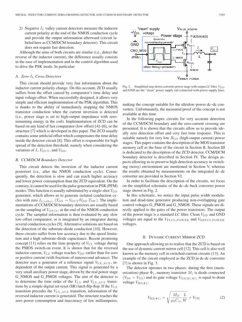
Fig. 2. Simplified step-down converter power stage with output LC filter. VDDand GND are the “clean” power supply rail connected with power supply lines.
making the concept suitable for the ultralow power dc–dc con-verters. Unfortunately, the measured proof of the concept is notavailable at this time.
In the following paper, circuits for very accurate detectionof the CCM/DCM boundary and the zero-current crossing arepresented. It is shown that the circuits allow us to provide ide-ally zero detection offset and very fast time response. This issuitable namely for very low RON (high-output current) powerstages. This paper contains the description of the MOS transistormemory cell as the base of the circuit in Section II. Section IIIis dedicated to the description of the ZCD detector. CCM/DCMboundary detector is described in Section IV. The design as-pects allowing us to preserve high detection accuracy in switch-ing (noisy) environment are mentioned in Section V, whereasthe results obtained by measurements on the integrated dc–dcconverter are provided in Section VI.
In order to facilitate the description of the circuits, we focuson the simplified schematic of the dc–dc buck converter powerstage shown in Fig. 2.
In this schematic, we notice the input pulse width modula-tion and dead-time generator producing non-overlapping gatecontrol voltages G_PMOS and G_NMOS. These signals are di-rectly applied to the gates of the power transistors. The outputof the power stage is a standard LC filter. Clean VDD and GNDvoltages are equal to the VPLUS POWER and VMINUS POWERvoltages.
II. DYNAMIC CURRENT MIRROR ZCD
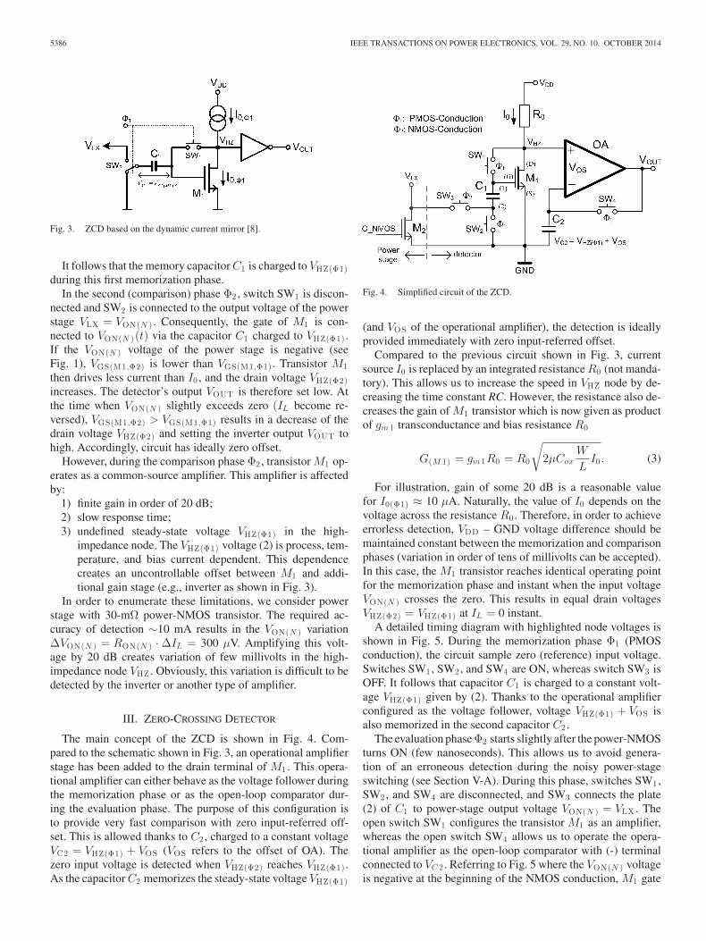
One approach allowing us to realize that the ZCD is based onthe use of dynamic current mirror cell [12]. This cell is also wellknown as the memory cell in switched-current circuits [13]. Anexample of the circuit employed as the ZCD in dc-dc converter[7] is shown in Fig. 3.
The detector operates in two phases: during the first (mem-orization) phase Φ1 , memory transistor M1 is diode connected(VDS = VGS) and its gate voltage VGS(M1,Φ1) is equal to drainvoltage VHZ(Φ1)
VHZ(Φ1) =
√2ID
μ0Cox
L
W+ VTH (2)
5386 IEEE TRANSACTIONS ON POWER ELECTRONICS, VOL. 29, NO. 10, OCTOBER 2014
Fig. 3. ZCD based on the dynamic current mirror [8].
It follows that the memory capacitor C1 is charged to VHZ(Φ1)during this first memorization phase.
In the second (comparison) phase Φ2 , switch SW1 is discon-nected and SW2 is connected to the output voltage of the powerstage VLX = VON(N ) . Consequently, the gate of M1 is con-nected to VON(N )(t) via the capacitor C1 charged to VHZ(Φ1) .If the VON(N ) voltage of the power stage is negative (seeFig. 1), VGS(M1,Φ2) is lower than VGS(M1,Φ1) . Transistor M1then drives less current than I0 , and the drain voltage VHZ(Φ2)increases. The detector’s output VOUT is therefore set low. Atthe time when VON(N ) slightly exceeds zero (IL become re-versed), VGS(M1,Φ2) > VGS(M1,Φ1) results in a decrease of thedrain voltage VHZ(Φ2) and setting the inverter output VOUT tohigh. Accordingly, circuit has ideally zero offset.
However, during the comparison phase Φ2 , transistor M1 op-erates as a common-source amplifier. This amplifier is affectedby:
1) finite gain in order of 20 dB;2) slow response time;3) undefined steady-state voltage VHZ(Φ1) in the high-
impedance node. The VHZ(Φ1) voltage (2) is process, tem-perature, and bias current dependent. This dependencecreates an uncontrollable offset between M1 and addi-tional gain stage (e.g., inverter as shown in Fig. 3).
In order to enumerate these limitations, we consider powerstage with 30-mΩ power-NMOS transistor. The required ac-curacy of detection ∼10 mA results in the VON(N ) variationΔVON(N ) = RON(N ) · ΔIL = 300 μV. Amplifying this volt-age by 20 dB creates variation of few millivolts in the high-impedance node VHZ . Obviously, this variation is difficult to bedetected by the inverter or another type of amplifier.
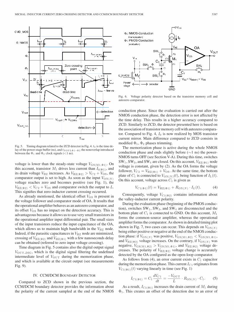
III. ZERO-CROSSING DETECTOR
The main concept of the ZCD is shown in Fig. 4. Com-pared to the schematic shown in Fig. 3, an operational amplifierstage has been added to the drain terminal of M1 . This opera-tional amplifier can either behave as the voltage follower duringthe memorization phase or as the open-loop comparator dur-ing the evaluation phase. The purpose of this configuration isto provide very fast comparison with zero input-referred off-set. This is allowed thanks to C2 , charged to a constant voltageVC2 = VHZ(Φ1) + VOS (VOS refers to the offset of OA). Thezero input voltage is detected when VHZ(Φ2) reaches VHZ(Φ1) .As the capacitor C2 memorizes the steady-state voltage VHZ(Φ1)
Fig. 4. Simplified circuit of the ZCD.
(and VOS of the operational amplifier), the detection is ideallyprovided immediately with zero input-referred offset.
Compared to the previous circuit shown in Fig. 3, currentsource I0 is replaced by an integrated resistance R0 (not manda-tory). This allows us to increase the speed in VHZ node by de-creasing the time constant RC. However, the resistance also de-creases the gain of M1 transistor which is now given as productof gm1 transconductance and bias resistance R0
G(M 1) = gm1R0 = R0
√2μCox
W
LI0 . (3)
For illustration, gain of some 20 dB is a reasonable valuefor I0(Φ1) ≈ 10 μA. Naturally, the value of I0 depends on thevoltage across the resistance R0 . Therefore, in order to achieveerrorless detection, VDD – GND voltage difference should bemaintained constant between the memorization and comparisonphases (variation in order of tens of millivolts can be accepted).In this case, the M1 transistor reaches identical operating pointfor the memorization phase and instant when the input voltageVON(N ) crosses the zero. This results in equal drain voltagesVHZ(Φ2) = VHZ(Φ1) at IL = 0 instant.
A detailed timing diagram with highlighted node voltages isshown in Fig. 5. During the memorization phase Φ1 (PMOSconduction), the circuit sample zero (reference) input voltage.Switches SW1 , SW2 , and SW4 are ON, whereas switch SW3 isOFF. It follows that capacitor C1 is charged to a constant volt-age VHZ(Φ1) given by (2). Thanks to the operational amplifierconfigured as the voltage follower, voltage VHZ(Φ1) + VOS isalso memorized in the second capacitor C2 .
The evaluation phase Φ2 starts slightly after the power-NMOSturns ON (few nanoseconds). This allows us to avoid genera-tion of an erroneous detection during the noisy power-stageswitching (see Section V-A). During this phase, switches SW1 ,SW2 , and SW4 are disconnected, and SW3 connects the plate(2) of C1 to power-stage output voltage VON(N ) = VLX . Theopen switch SW1 configures the transistor M1 as an amplifier,whereas the open switch SW4 allows us to operate the opera-tional amplifier as the open-loop comparator with (-) terminalconnected to VC 2 . Referring to Fig. 5 where the VON(N ) voltageis negative at the beginning of the NMOS conduction, M1 gate
MICHAL: INDUCTOR CURRENT ZERO-CROSSING DETECTOR AND CCM/DCM BOUNDARY DETECTOR 5387
Fig. 5. Timing diagram related to the ZCD detector in Fig. 4. t0 is the time de-lay of the power-stage buffer (ns), and tNOVLΦ1−Φ2 the nonoverlap introducedbetween the Φ1 and Φ2 clock signals (<1 ns).
voltage is lower than the steady-state voltage VGS(M1,Φ1) . Onthis account, transistor M1 drives less current than I0(Φ1) , andits drain voltage VHZ increases. As VHZ(Φ2) > VC 2 + VOS , thecomparator output is set to high. As soon as the input VON(N )voltage reaches zero and becomes positive (see Fig. 1), theVHZ(Φ2) < VC 2 + VOS and comparator switch the output to L.This signifies that zero-inductor current crossing occurred.
As already mentioned, the identical offset VOS is present inthe voltage follower and comparator mode of OA. It results thatthe operational amplifier behaves as an autozero comparator, andits offset VOS has no impact on the detection accuracy. This isadvantageous because it allows us to use very small transistors inthe operational amplifier input differential pair. The small sizesof the input transistors reduce the input capacitance of the OA,which allows us to maintain high bandwidth in the VHZ node.Indeed, if the parasitic capacitances in VHZ node are minimized,crossing of VHZ(Φ2) and VHZ(Φ1) with a few nanoseconds delaycan be obtained (referred to zero input voltage crossing).
Time diagram in Fig. 5 contains also the digital output signalVOUT DIG , which is the digital signal filtering the undefinedintermediate level of VOUT during the memorization phase,and which is available at the circuit output (see measurementsFig. 9).
IV. CCM/DCM BOUNDARY DETECTOR
Compared to ZCD shown in the previous section, theCCM/DCM boundary detector provides the information aboutthe polarity of the current sampled at the end of the NMOS
Fig. 6. Voltage polarity detector based on the transistor memory cell andautozero comparator.
conduction phase. Since the evaluation is carried out after theNMOS conduction phase, the detection error is not affected bythe time delay. This results in a higher accuracy compared toZCD. Similarly to ZCD, the detector presented here is based onthe association of transistor memory cell with autozero compara-tor. Compared to Fig. 4, I0 is now realized by MOS transistorcurrent mirror. Main difference compared to ZCD consists inmodified Φ1 , Φ2 phases trimming.
The memorization phase is active during the whole NMOSconduction phase and ends slightly before (∼1 ns) the power-NMOS turns OFF (see Section V-A). During this time, switchesSW1 , SW3 , and SW4 are closed. On this account, VHZ(Φ1) nodevoltage is constant, given by (2). As the OA forms the voltagefollower, VC 2 = VHZ(Φ1) + VOS . At the same time, the bottomplate of C1 is connected to VON(N )(t), being function of IL(t).On this account, voltage across C1 is given as
VC 1(Φ1)(t) = VHZ(Φ1) + RON(N ) · IL (t). (4)
Consequently, voltage VC1(Φ2) contains information aboutthe valley-inductor current polarity.
During the evaluation phase (beginning of the PMOS conduc-tion), switches SW1 , SW3 , and SW4 are disconnected and thebottom plate of C1 is connected to GND. On this account, M1forms the common-source amplifier, whereas the operationalamplifier forms the comparator. As shown in detailed timing plotshown in Fig. 7, two cases can occur. This depends on VON(N )being either positive or negative at the end of the NMOS conduc-tion phase: if VON(N ) was positive, VGS(M1,Φ2) < VGS(M1,Φ1) ,and VHZ(Φ2) voltage increases. On the contrary, if VON(N ) wasnegative, VGS(M1,Φ2) > VGS(M1,Φ1) , and VHZ(Φ2) voltage de-creases. The polarity of VHZ(Φ2) voltage change is accuratelydetected by the OA configured as the open-loop comparator.
As follows from (4), an error current exists in C1 capacitorduring the memorization phase. This current IC 1 originates fromVC1(Φ1)(t) varying linearly in time (see Fig. 1)
IC 1(Φ1) = C1dVC 1
dt=
−VOUT
L· RON(N ) · C1 . (5)
As a result, IC1(Φ1) increases the drain current of M1 duringΦ1 . This creates an offset of the detection due to an error of
5388 IEEE TRANSACTIONS ON POWER ELECTRONICS, VOL. 29, NO. 10, OCTOBER 2014
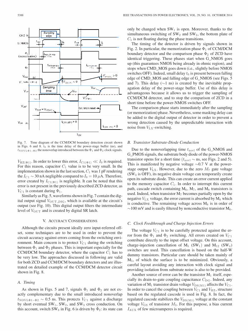
Fig. 7. Time diagram of the CCM/DCM boundary detection circuit shownin Figs. 6 and 8. t0 is the time delay of the power-stage buffer (ns), andtNOVLΦ1−Φ2 the nonoverlap introduced between the Φ1 and Φ2 clock signals.
VHZ(Φ1) . In order to lower this error, IC1(Φ1) << I0 is required.For this reason, capacitor C1 value is to be very small. In theimplementation shown in the last section, C1 was 1 pF renderingthe IC 1 ∼ 30 nA negligible compared to I0 = 10 μA. Therefore,error created by IC1(Φ1) is negligible. It can be noted that thiserror is not present in the previously described ZCD detector, asVC 1 is constant during Φ1 .
Similarly as Fig. 5, waveforms shown in Fig. 7 contain the dig-ital output signal VOUT DIG , which is available at the circuit’soutput (see Fig. 10). This digital output filters the intermediatelevel of VOUT and is created by digital SR latch.
V. ACCURACY CONSIDERATIONS
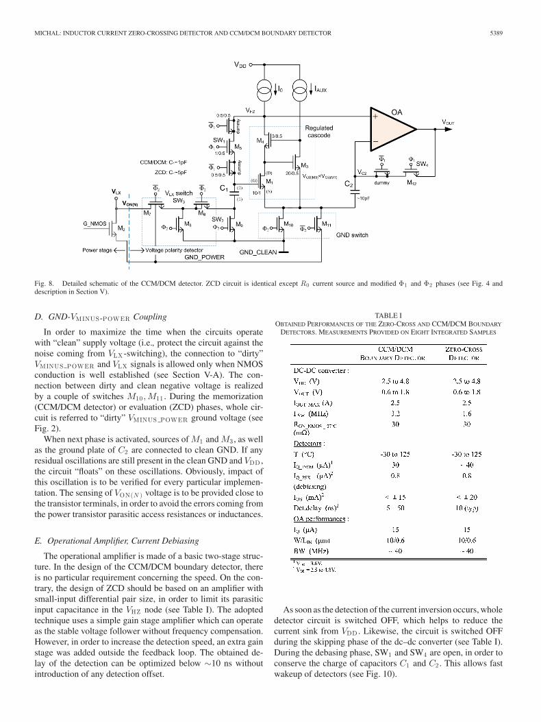
Although the circuits present ideally zero input-referred off-set, some techniques are to be used in order to prevent thecircuit accuracy against errors coming from the switching envi-ronment. Main concern is to protect VC 1 during the switchingbetween Φ1 and Φ2 phases. This is important especially for theCCM/DCM boundary detector, where the capacitor C1 has tobe very low. The approaches discussed in following are validfor both ZCD and CCM/DCM boundary detectors and are illus-trated on detailed example of the CCM/DCM detector circuitshown in Fig. 8.
A. Timing
As shown in Figs. 5 and 7, signals Φ1 and Φ2 are not ex-actly complementary due to the small introduced nonoverlaptNOVLΦ1−Φ2 ∼ 0.5 ns. This protects VC 1 against a dischargeby short eventual SW1 , SW2 , and SW3 cross conduction. Onthis account, switch SW3 in Fig. 6 is driven by Φ2 : its state can
only be changed when SW1 is open. Moreover, thanks to thesimultaneous switching of SW2 and SW3 , the bottom plate ofC1 is not floating during the phase transitions.
The timing of the detector is driven by signals shown inFig. 2. In particular, the memorization phase Φ1 of CCM/DCMboundary detector and the comparison phase Φ2 of ZCD haveidentical triggering. These phases start when G_NMOS goesup (this guarantees NMOS being already in ohmic region), andstops when CMD_MOS goes down (i.e., slightly before NMOSswitches OFF). Indeed, small delay t0 is present between fallingedge of CMD_MOS and falling edge of G_NMOS (see Figs. 5and 7). This delay (∼1 ns) is created by the inevitable prop-agation delay of the power-stage buffer. Use of this delay isadvantageous because it allows us to trigger the sampling ofCCM/DCM detector, and to stop the comparison of ZCD in ashort time before the power-NMOS switches OFF.
The comparison phase starts immediately after the sampling(or memorization) phase. Nevertheless, some masking delay canbe added to the digital output of detector in order to prevent awrong detection caused by the unpredictable interaction withnoise from VLX -switching.
B. Transistor Substrate-Diode Conduction
Due to the nonoverlapping time tnovl of the G_NMOS andG_PMOS signals, the substrate body diode of the power-NMOStransistor opens for a short time (tnovl ∼ ns, see Figs. 2 and 5).This is manifested by negative voltage ∼0.7 V at the power-stage output VLX . However, due to the zero M7 gate voltage(SW3 is OFF), its negative drain voltage can temporarily createopen its substrate diode. This can create an error current appliedto the memory capacitor C1 . In order to interrupt this currentpath, cascade switch containing M6 , M7 , and M8 transistors isused. Indeed, when transistor M7 becomes partially open by thenegative VLX voltage, the error current is absorbed by M8 whichis conductive. The remaining voltage across M8 is in order of∼100 mV and is easily filtered by nonconductive transistor M6 .
C. Clock Feedthrough and Charge Injection Errors
The voltage VC 1 is to be carefully protected against the er-ror from the Φ1 and Φ2 switching. All errors created on VC 1contribute directly to the input offset voltage. On this account,charge-injection cancellation of M5 (SW1) and M12 (SW4)switches are used. This cancellation is based on the half-Wdummy transistors. Particular care should be taken mainly ofM5 , of which the surface is to be minimized. Obviously, acareful layout avoiding any interaction with clock signal andproviding isolation from substrate noise is also to be provided.
Another source of error can be the transistor M1 itself, espe-cially its drain-to-gate coupling capacitance CDG . Indeed, anyvariation of M1 transistor drain voltage VDS(M1) affects the VC1 .In order to cancel the coupling between VC1 and VHZ , structurebased on the regulated cascode is used in Fig. 8. In fact, theregulated cascode stabilizes the VDS(M1) voltage at the constantvoltage VGS of transistor M3 . For this purpose, a bias currentIAUX of few microamperes is required.
MICHAL: INDUCTOR CURRENT ZERO-CROSSING DETECTOR AND CCM/DCM BOUNDARY DETECTOR 5389
Fig. 8. Detailed schematic of the CCM/DCM detector. ZCD circuit is identical except R0 current source and modified Φ1 and Φ2 phases (see Fig. 4 anddescription in Section V).
D. GND-VMINUS-POWER Coupling
In order to maximize the time when the circuits operatewith “clean” supply voltage (i.e., protect the circuit against thenoise coming from VLX -switching), the connection to “dirty”VMINUS POWER and VLX signals is allowed only when NMOSconduction is well established (see Section V-A). The con-nection between dirty and clean negative voltage is realizedby a couple of switches M10 ,M11 . During the memorization(CCM/DCM detector) or evaluation (ZCD) phases, whole cir-cuit is referred to “dirty” VMINUS POWER ground voltage (seeFig. 2).
When next phase is activated, sources of M1 and M3 , as wellas the ground plate of C2 are connected to clean GND. If anyresidual oscillations are still present in the clean GND and VDD ,the circuit “floats” on these oscillations. Obviously, impact ofthis oscillation is to be verified for every particular implemen-tation. The sensing of VON(N ) voltage is to be provided close tothe transistor terminals, in order to avoid the errors coming fromthe power transistor parasitic access resistances or inductances.
E. Operational Amplifier, Current Debiasing
The operational amplifier is made of a basic two-stage struc-ture. In the design of the CCM/DCM boundary detector, thereis no particular requirement concerning the speed. On the con-trary, the design of ZCD should be based on an amplifier withsmall-input differential pair size, in order to limit its parasiticinput capacitance in the VHZ node (see Table I). The adoptedtechnique uses a simple gain stage amplifier which can operateas the stable voltage follower without frequency compensation.However, in order to increase the detection speed, an extra gainstage was added outside the feedback loop. The obtained de-lay of the detection can be optimized below ∼10 ns withoutintroduction of any detection offset.
TABLE IOBTAINED PERFORMANCES OF THE ZERO-CROSS AND CCM/DCM BOUNDARY
DETECTORS. MEASUREMENTS PROVIDED ON EIGHT INTEGRATED SAMPLES
As soon as the detection of the current inversion occurs, wholedetector circuit is switched OFF, which helps to reduce thecurrent sink from VDD . Likewise, the circuit is switched OFFduring the skipping phase of the dc–dc converter (see Table I).During the debasing phase, SW1 and SW4 are open, in order toconserve the charge of capacitors C1 and C2 . This allows fastwakeup of detectors (see Fig. 10).
5390 IEEE TRANSACTIONS ON POWER ELECTRONICS, VOL. 29, NO. 10, OCTOBER 2014
Fig. 9. Measurement of the ZCD circuit for VDD = 3.6 V.
F. Other Limitations
Although the detectors presented here reach ideally zeroinput-referred offset, the use in noisy-switched environment caninfluence the total detection accuracy. This can be accentuatedby the dc–dc converter architecture based on the external powerswitches. Another aspect encountered in the design was the ex-treme duty-cycle operations, where the internal capacitor is notproperly charged due to the limited charging time. The minimumtime required for the correct circuit operation was revealed inorder of ∼10 ns.
VI. MEASURED RESULTS
Described circuits of CCM/DCM boundary detector andZCD detector were implemented in 130-nm ST CMOS process(5-V transistors with LMIN = 0.5 μm) and were integrated inthe control part of 2.5-A step-down dc–dc converters with 30-mΩ power NMOS and 1-μH inductor. The responses of thedetectors were observed by the digital kelvin access. Presenteddetectors were designed for the new mobiles and tablets power-management platform and are also intended to be embedded inthe dc–dc converter of 40-nm STM microprocessors. The perfor-mances were also validated in research applications [14], [15].
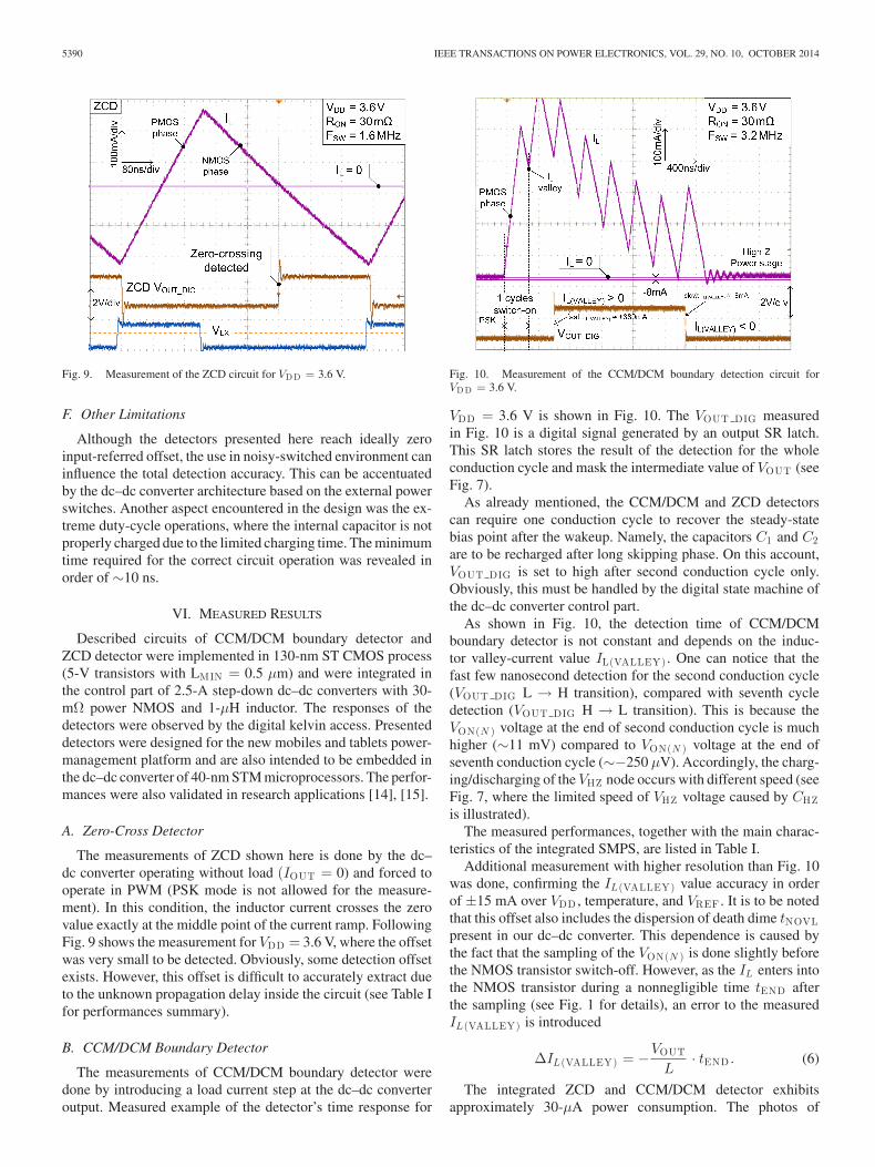
A. Zero-Cross Detector
The measurements of ZCD shown here is done by the dc–dc converter operating without load (IOUT = 0) and forced tooperate in PWM (PSK mode is not allowed for the measure-ment). In this condition, the inductor current crosses the zerovalue exactly at the middle point of the current ramp. FollowingFig. 9 shows the measurement for VDD = 3.6 V, where the offsetwas very small to be detected. Obviously, some detection offsetexists. However, this offset is difficult to accurately extract dueto the unknown propagation delay inside the circuit (see Table Ifor performances summary).
B. CCM/DCM Boundary Detector
The measurements of CCM/DCM boundary detector weredone by introducing a load current step at the dc–dc converteroutput. Measured example of the detector’s time response for
Fig. 10. Measurement of the CCM/DCM boundary detection circuit forVDD = 3.6 V.
VDD = 3.6 V is shown in Fig. 10. The VOUT DIG measuredin Fig. 10 is a digital signal generated by an output SR latch.This SR latch stores the result of the detection for the wholeconduction cycle and mask the intermediate value of VOUT (seeFig. 7).
As already mentioned, the CCM/DCM and ZCD detectorscan require one conduction cycle to recover the steady-statebias point after the wakeup. Namely, the capacitors C1 and C2are to be recharged after long skipping phase. On this account,VOUT DIG is set to high after second conduction cycle only.Obviously, this must be handled by the digital state machine ofthe dc–dc converter control part.
As shown in Fig. 10, the detection time of CCM/DCMboundary detector is not constant and depends on the induc-tor valley-current value IL(VALLEY) . One can notice that thefast few nanosecond detection for the second conduction cycle(VOUT DIG L → H transition), compared with seventh cycledetection (VOUT DIG H → L transition). This is because theVON(N ) voltage at the end of second conduction cycle is muchhigher (∼11 mV) compared to VON(N ) voltage at the end ofseventh conduction cycle (∼−250 μV). Accordingly, the charg-ing/discharging of the VHZ node occurs with different speed (seeFig. 7, where the limited speed of VHZ voltage caused by CHZis illustrated).
The measured performances, together with the main charac-teristics of the integrated SMPS, are listed in Table I.
Additional measurement with higher resolution than Fig. 10was done, confirming the IL(VALLEY) value accuracy in orderof ±15 mA over VDD , temperature, and VREF . It is to be notedthat this offset also includes the dispersion of death dime tNOVLpresent in our dc–dc converter. This dependence is caused bythe fact that the sampling of the VON(N ) is done slightly beforethe NMOS transistor switch-off. However, as the IL enters intothe NMOS transistor during a nonnegligible time tEND afterthe sampling (see Fig. 1 for details), an error to the measuredIL(VALLEY) is introduced
ΔIL(VALLEY) = −VOUT
L· tEND . (6)
The integrated ZCD and CCM/DCM detector exhibitsapproximately 30-μA power consumption. The photos of
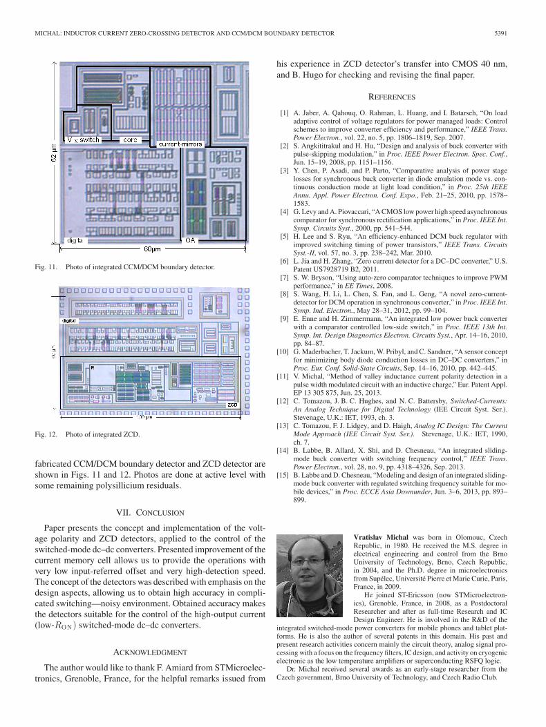
MICHAL: INDUCTOR CURRENT ZERO-CROSSING DETECTOR AND CCM/DCM BOUNDARY DETECTOR 5391
Fig. 11. Photo of integrated CCM/DCM boundary detector.
Fig. 12. Photo of integrated ZCD.
fabricated CCM/DCM boundary detector and ZCD detector areshown in Figs. 11 and 12. Photos are done at active level withsome remaining polysillicium residuals.
VII. CONCLUSION
Paper presents the concept and implementation of the volt-age polarity and ZCD detectors, applied to the control of theswitched-mode dc–dc converters. Presented improvement of thecurrent memory cell allows us to provide the operations withvery low input-referred offset and very high-detection speed.The concept of the detectors was described with emphasis on thedesign aspects, allowing us to obtain high accuracy in compli-cated switching—noisy environment. Obtained accuracy makesthe detectors suitable for the control of the high-output current(low-RON) switched-mode dc–dc converters.
ACKNOWLEDGMENT
The author would like to thank F. Amiard from STMicroelec-tronics, Grenoble, France, for the helpful remarks issued from
his experience in ZCD detector’s transfer into CMOS 40 nm,and B. Hugo for checking and revising the final paper.
REFERENCES
[1] A. Jaber, A. Qahouq, O. Rahman, L. Huang, and I. Batarseh, “On loadadaptive control of voltage regulators for power managed loads: Controlschemes to improve converter efficiency and performance,” IEEE Trans.Power Electron., vol. 22, no. 5, pp. 1806–1819, Sep. 2007.
[2] S. Angkititrakul and H. Hu, “Design and analysis of buck converter withpulse-skipping modulation,” in Proc. IEEE Power Electron. Spec. Conf.,Jun. 15–19, 2008, pp. 1151–1156.
[3] Y. Chen, P. Asadi, and P. Parto, “Comparative analysis of power stagelosses for synchronous buck converter in diode emulation mode vs. con-tinuous conduction mode at light load condition,” in Proc. 25th IEEEAnnu. Appl. Power Electron. Conf. Expo., Feb. 21–25, 2010, pp. 1578–1583.
[4] G. Levy and A. Piovaccari, “A CMOS low power high speed asynchronouscomparator for synchronous rectification applications,” in Proc. IEEE Int.Symp. Circuits Syst., 2000, pp. 541–544.
[5] H. Lee and S. Ryu, “An efficiency-enhanced DCM buck regulator withimproved switching timing of power transistors,” IEEE Trans. CircuitsSyst.-II, vol. 57, no. 3, pp. 238–242, Mar. 2010.
[6] L. Jia and H. Zhang, “Zero current detector for a DC–DC converter,” U.S.Patent US7928719 B2, 2011.
[7] S. W. Bryson, “Using auto-zero comparator techniques to improve PWMperformance,” in EE Times, 2008.
[8] S. Wang, H. Li, L. Chen, S. Fan, and L. Geng, “A novel zero-current-detector for DCM operation in synchronous converter,” in Proc. IEEE Int.Symp. Ind. Electron., May 28–31, 2012, pp. 99–104.
[9] E. Enne and H. Zimmermann, “An integrated low power buck converterwith a comparator controlled low-side switch,” in Proc. IEEE 13th Int.Symp. Int. Design Diagnostics Electron. Circuits Syst., Apr. 14–16, 2010,pp. 84–87.
[10] G. Maderbacher, T. Jackum, W. Pribyl, and C. Sandner, “A sensor conceptfor minimizing body diode conduction losses in DC–DC converters,” inProc. Eur. Conf. Solid-State Circuits, Sep. 14–16, 2010, pp. 442–445.
[11] V. Michal, “Method of valley inductance current polarity detection in apulse width modulated circuit with an inductive charge,” Eur. Patent Appl.EP 13 305 875, Jun. 25, 2013.
[12] C. Tomazou, J. B. C. Hughes, and N. C. Battersby, Switched-Currents:An Analog Technique for Digital Technology (IEE Circuit Syst. Ser.).Stevenage, U.K.: IET, 1993, ch. 3.
[13] C. Tomazou, F. J. Lidgey, and D. Haigh, Analog IC Design: The CurrentMode Approach (IEE Circuit Syst. Ser.). Stevenage, U.K.: IET, 1990,ch. 7.
[14] B. Labbe, B. Allard, X. Shi, and D. Chesneau, “An integrated sliding-mode buck converter with switching frequency control,” IEEE Trans.Power Electron., vol. 28, no. 9, pp. 4318–4326, Sep. 2013.
[15] B. Labbe and D. Chesneau, “Modeling and design of an integrated sliding-mode buck converter with regulated switching frequency suitable for mo-bile devices,” in Proc. ECCE Asia Downunder, Jun. 3–6, 2013, pp. 893–899.
Vratislav Michal was born in Olomouc, CzechRepublic, in 1980. He received the M.S. degree inelectrical engineering and control from the BrnoUniversity of Technology, Brno, Czech Republic,in 2004, and the Ph.D. degree in microelectronicsfrom Supelec, Universite Pierre et Marie Curie, Paris,France, in 2009.
He joined ST-Ericsson (now STMicroelectron-ics), Grenoble, France, in 2008, as a PostdoctoralResearcher and after as full-time Research and ICDesign Engineer. He is involved in the R&D of the
integrated switched-mode power converters for mobile phones and tablet plat-forms. He is also the author of several patents in this domain. His past andpresent research activities concern mainly the circuit theory, analog signal pro-cessing with a focus on the frequency filters, IC design, and activity on cryogenicelectronic as the low temperature amplifiers or superconducting RSFQ logic.
Dr. Michal received several awards as an early-stage researcher from theCzech government, Brno University of Technology, and Czech Radio Club.